1
Application Note 9840
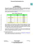
Appendix B Pin Descriptions
PIN NO.
39-32
PIN NAME
PIN DESCRIPTION
QD7 (MSB) Through Digital Data Bit 7, the Most Significant Bit through Digital Data Bit 0, the Least Significant Bit, of the Q
QD0 (LSB)
channel.
1-5, 48-46
ID7 (MSB) Through
ID0 (LSB)
Digital Data Bit 7, the Most Significant Bit through Digital Data Bit 0, the Least Significant Bit, of the I
channel.
8
SLEEP
Control Pin for Power-Down Mode. Sleep Mode is active high; connect to ground for Normal Mode. Sleep
pin has internal 20µA active pulldown current.
15
REFLO
Connect to analog ground to enable internal 1.2V reference or connect to AVDD to disable.
23
REFIO
Reference voltage input if internal reference is disabled and reference voltage output if internal reference is
enabled. Use 0.1µF cap to ground when internal reference is enabled.
22
FSADJ
Full Scale Current Adjust. Use a resistor to ground to adjust full scale output current. Full Scale Output
Current Per Channel = 32 x IFSADJ .
14, 24
ICOMP1, QCOMP1
For use in reducing bandwidth/noise of the I and Q channels. Recommended: connect 0.1µF to AVDD
as close as possible to each of the pins. These two pins MUST be connected together externally.
13, 18, 19, 25
AGND
Analog Ground Connections.
17
IOUTB
The complementary current output of the I Channel. Bits set to all 0s gives full scale current.
16
IOUTA
Current output of the I channel. Bits set to all 1s gives full scale current.
20
QOUTB
The complementary current output of the Q Channel. Bits set to all 0s gives full scale current.
21
QOUTA
Current output of the Q Channel. Bits set to all 1s gives full scale current.
11, 27
NC
12, 26
AVDD
Analog Supply (+2.7V to +5.5V).
6, 7, 10, 28, 30,
31, 41, 44
DGND
Digital Ground.
9, 29, 40, 45
DVDD
Supply voltage for digital circuitry (+2.7V to +5.5V).
43
ICLK
Clock input for I Channel. Positive edge of clock latches data.
42
QCLK
Clock input for Q Channel. Positive edge of clock latches data.
No Connect. Recommended: Connect to ground.
6