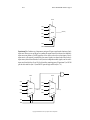
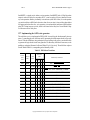
1
Lab
B441 LABORATORY MANUAL page 1
Indiana University
Computer Science B441/B541
Laboratory Experiments
Fall 1998
Franklin Prosser, David Winkel, and David Wilson
© 1998 Franklin Prosser
Revised 1999 Steven D. Johnson and Caleb Hess
DRAFT January 29, 2001
[email protected]
Copyright ©2000 Indiana University Computer Science Department
Lab 0
B441 LABORATORY MANUAL page 2
Laboratory 0 Document defaults
This is the template file for the Lab manual. All common formats should have instances in this
file, so that they can be imported into the book.
Some good things to know about include:
• system variables [ch. 7 of the Framemaker manual]
• autonumbering [ch 4]. Sections, subsections, figures, and tables are numbered using series L
0.1 Cataloged character formats
Catalog character styles include
SIGNAL
helvetica, upper case
NETGATEDSIGNAL
helvetica, upper case, overba
0.2 HeaderA Style
0.2.1 HeadeB Style
subsec style
Indentation schemes
Indented paragraph styles include:
Indent1
Indent2
Indent3
Indent4
Indent5
• ul: the quick brown fox jumped over the very lazy dog the quick brown fox jumped over the
lazy dog.
1. ol: the quick brown fox jumped over the very lazy dog the quick brown fox jumped over the
lazy dog.
Copyright ©2000 Indiana University Computer Science Department
Lab 0
B441 LABORATORY MANUAL page 3
0.3 Some table formats
Format C
A
B
C
D
Table 0-1 Format B
Signal Level
TTL voltage Ranges
CMOS Voltage Ranges
L
0.0 - 0.8 V
0.0 - 1.0 V
H
2.0 - 5.0 V
3.5 - 5.0 V
Table 0-2 Format A
0.4 Figures
For example,
Text within figure
Figure 0-1
0.5 Graphic Symbols
Set grid-snap to .0625" and grid lines to .125".
For signal names use helvetica, 10pt: ABCD, ABCD
Copyright ©2000 Indiana University Computer Science Department
Lab 0
B441 LABORATORY MANUAL page 4
0.6 Basic gates
.
0
0
0
0
1
1
1
1
Copyright ©2000 Indiana University Computer Science Department
Lab 0
B441 LABORATORY MANUAL page 5
0.7 Storage elements
Q
T
D
Q
CLK
R
Q
Q
Q
J
Q
K
S
Q
R
Q
S
Q
Q
Copyright ©2000 Indiana University Computer Science Department
Lab 0
B441 LABORATORY MANUAL page 6
0.7.1 Analog components
H
T
..
.
Copyright ©2000 Indiana University Computer Science Department
Lab
B441 LABORATORY MANUAL page 7
Lab 0: Document defaults................................................................. 2
0.1 Cataloged character formats ......................................................................... 2
0.2 HeaderA Style............................................................................................... 2
0.3 Some table formats ....................................................................................... 3
0.4 Figures........................................................................................................... 3
0.5 Graphic Symbols........................................................................................... 3
0.6 Basic gates .................................................................................................... 4
0.7 Storage elements ........................................................................................... 5
Lab 1: Introduction to your laboratory tools................................ 10
0.1 Basics .......................................................................................................... 10
0.2 The Logic Engine........................................................................................ 16
0.3 Experiments ................................................................................................ 17
0.4 Appendix: Using the Logic Engine Board in B441/B541 .......................... 20
Lab 2: Mixed logic........................................................................... 24
0.1 Experiments ................................................................................................ 25
Lab 3: Three-state logic .................................................................. 30
0.1 Experiments ................................................................................................ 32
Lab 4: Programmable logic ............................................................ 35
0.1 The Xilinx FPGA........................................................................................ 37
0.2 Experiments ................................................................................................ 38
Lab 5: Synthesis of combinational elements ................................. 39
0.1 Seven-segment display decoder .................................................................. 39
0.2 The Multiplexer........................................................................................... 39
0.3 Automated testing with the Logic Engine -- an optional way to test complex devices 41
Lab 6: Hierarchical Design Using Schematic Macros.................. 43
0.1 Introduction to Schematic Macros .............................................................. 43
0.2 Creating a Macro Component for a 1-bit Magnitude Comparator ............. 44
0.3 Creating a Macro Component for a 4-bit Comparator................................ 45
0.4 Scaling the 4-bit Magnitude Comparator to Build an 8-bit Comparator .... 45
Lab 7: Synthesizing an ALU .......................................................... 46
0.1 Making a 4-bit logic unit............................................................................. 46
0.2 Making a 4-bit arithmetic unit .................................................................... 48
0.3 Experiments ............................................................................................... 48
Copyright ©2000 Indiana University Computer Science Department
Lab
B441 LABORATORY MANUAL page 8
Lab 8: Sequential circuits -- Counters........................................... 50
0.1 Experiments ................................................................................................ 52
Lab 9: Register-transfer concepts.................................................. 56
0.1 Experiments: ............................................................................................... 57
Lab 10: Building the PDP-8 data path .......................................... 61
0.1 Experiments: ............................................................................................... 65
Lab 11: Manual ASM Control of the PDP-8 ................................ 73
0.1 Completing the data path ............................................................................ 73
0.2 Setting up Manual Control.......................................................................... 73
0.3 Basic instruction execution ......................................................................... 75
0.4 Here an Address, there an Address ............................................................. 76
Lab 12: Building the PDP-8 controller.......................................... 80
0.1 The ASM chart............................................................................................ 80
0.2 The fetch phase. .......................................................................................... 80
0.3 How the laboratory ASM relates to the textbook ASM.............................. 81
0.4 An early (and temporary) shortcut, if you care to use it. ............................ 81
0.5 A few additional pieces of hardware........................................................... 82
0.6 Completing the PDP-8 architecture. ........................................................... 82
0.7 Implementing the ASM’s state generator.................................................... 83
0.8 Packaging the ASM’s outputs..................................................................... 84
0.9 Implementing the ASM outputs.................................................................. 84
Lab 13: Debugging and testing your PDP-8 processor ................ 86
0.1 How to debug using the diagnostic programs. ............................................ 86
0.2 Using Instruction Test 1. ............................................................................. 87
0.3 Installing an input/output interface and running “real” programs. ............. 87
Lab 14: Building a Serial Interface for the PDP-8 ....................... 89
0.1 Serial Data Format. ..................................................................................... 89
0.2 The Baud Rate Clock. ................................................................................. 90
0.3 Parallel to Serial Converter. ........................................................................ 90
0.4 Serial to Parallel Converter ......................................................................... 90
0.5 The Edge-Triggered RS Flip-Flop. ............................................................. 91
0.6 Practical Considerations.............................................................................. 92
Lab 15: Microcode Control ............................................................ 94
0.1 Hardware changes....................................................................................... 94
Copyright ©2000 Indiana University Computer Science Department
Lab
B441 LABORATORY MANUAL page 9
0.2 Designing the Microprogram...................................................................... 94
0.3 Microcode programming ............................................................................ 95
Appendix 1: Laboratory Drawings................................................ 96
Copyright ©2000 Indiana University Computer Science Department
Lab 1
B441 LABORATORY MANUAL page 10
Laboratory 1 Introduction to your laboratory tools
Your assignment for the semester in the B441/B541 laboratory is to build a simple yet complete
12-bit computer and run diagnostics on it. To achieve success, you must become familiar with the
equipment available to you. The first labs will introduce these tools. In these early labs you will be
guided step by step; later labs will provide only general directions and you will be expected to
proceed on your own. Some of the labs will require more than one week.
1.1 Basics
1.1.1 Wire wrapping
According to the old saying, you can tell a mechanic by his tools. If you ever see a mechanic use a
wrench as a hammer, take your car to another shop next time. A similar principle applies in this
lab. Students who understand and respect their tools and know when to use each one invariably
get done faster and derive more satisfaction from the project.
Your wirewrap tools are used at every turn in your project. Although simple, they can do lots of
damage. Take pride in your workmanship; it pays! An article reproduced at the end of this chapter
has photographs of good and bad technique. Photo 4 in that article shows what a proper wrap
looks like. Strive to make all your wraps look like this.
Wirewrapping works by forcing the wire into close contact at the corners of a square post. The
enormous pressure resulting from the wrapping action breaks down surface oxide layers and
allows the metals in the wire and the post to fuse. Scanning electron microscope pictures of wire
peeled from a perfect wrap conclusively show many small areas of cold welding between wire
and post. These welds are the result of atomic bonding between the two metals and are responsible for the impressive reliability of wire wrap technology. One manufacturer's study showed not a
single fault traceable to wirewrap in their customer base of installed computers.
A good wrap starts with a properly cut and stripped wire. If your wire is too short, its insulation
will be short and will not reach the destination post. The exposed bare wire may contact adjacent
posts or signal traces on the circuit board. If the wire is too long, you will soon have an awkward
three dimensional mat of wires. If you nick the wire when stripping insulation, the wire can break.
If it breaks inside the insulation you can have a perfectly good-looking wrap with intermittent
connection, something you really don't want. Proper cut-and-strip technique takes only a few minutes to master. Your lab AI will demonstrate the motion for a clean cut and strip.
Next, the stripped end of the wire is inserted into the business end of a wire-wrap tool. Slide the
wire in until the insulation bottoms inside the tool (or, with some tools, until you can see the
beginning of the insulation through the peephole). Enough insulated wire will then be in the tool
to cause the first turn of the wrap to be of insulated wire. This is very important. It will prevent
shorts to adjacent posts. The stripping tool leaves the right length of wire for 8 turns of bare wire.
(In the accompanying article, Photo 4 shows 15 turns; 8 are adequate.) Place the wrap tool and
Copyright ©2000 Indiana University Computer Science Department
Lab 1
B441 LABORATORY MANUAL page 11
wire over a post, put just enough tension on the wire to prevent the wrap tool from pulling extra
turns of insulated wire around the base of the post. If you twist the wrap tool while pushing down
with the right amount of pressure, the turns of bare wire will form a perfect helix with no space
between them, as in Photo 4. Push too hard, and you get a miniature wad of wire where one turn
rides up on top of previous turns (Photo 5). These wads of wire are distinctly poor form. If severe,
they can contact adjacent posts. Too little pressure and you get the mess shown in Photo 6. The
loose helix takes up unnecessary space and may not leave enough room to get a second wire on
the same post. Also, guess where the tail end of the wire sticking up will go? Murphy’s Law
ensures that it will end up touching a nearby post. Practice making single-ended wraps on your
board until you can make every one look like Photo 4.
The other end of the wire is important, too. The proper technique is to pull the wire in a straight
line moderately tight over the destination post and insert the wire into the stripping blade of your
cut-and-strip tool about 0.2 inch past this post. While maintaining tension, swing the open cutters
over the wire, cutting the wire and stripping the insulation. Properly done, you will have a wire
with enough insulation length to form one or two turns of insulation around the target post. If you
don't have this much length, replace the wire.
The unwrapping tool is used to remove bad wraps. It has a very sharp knife edge that will slip
between turns when rotated. Practice unwrapping until you know how much pressure to use. This
tool will work only in the counterclockwise direction. This argues strongly that you should turn
the wrap tool in the clockwise direction when you make your wraps!. Don't drop the tools. The
unwrapper always seems to land on the sharp point. The wrapper always lands on the end and
snaps the hardened steel shank.
A daisy chain connects multiple posts with a series of single wirewraps. The proper technique is
shown in Photo 9 of the article. Why don't you want your daisy chains to look like Photo 8?
1.1.2 Inserting integrated circuit chips into sockets
Most of the integrated circuits (ICs or “chips”) that you will use in the lab have been used before.
Their pins may be bent. Before you try inserting an IC into a socket, be sure that all the pins are
straight. Use your needle-nose pliers. If the IC is new, the pins will be splayed out (to facilitate
automated insertion at factories) and must be bent perpendicular to the IC body. To do this, press
the IC firmly on the table and rock it until the row of pins is at right angles to the chip, as in Figure
Copyright ©2000 Indiana University Computer Science Department
Lab 1
B441 LABORATORY MANUAL page 12
1-1. If you don't press firmly enough, Figure 1-1 (right) is the (bad) result.
(b)
(a)
(c)
Figure 1-1
Now insert the IC into the socket by tilting until one row of pins enters the socket. You can usually
tell by feel if they are properly lined up. Push gently. Again, you can feel if all pins are going in
smoothly. The worst bug you can introduce in your system is shown in Figure 1-2. The problem
here is that the bent lead makes contact initially and then fails intermittently during finals week.
1.1.3 Removing ICs from sockets
Slip the ends of the chip puller under a chip, then gently pull up while rocking the puller slightly
from end to end. The motion is akin to “walking” the chip out of the socket; first one end a tiny
bit, then the other. To avoid results such as in Fig. 1-3, always use the puller when extracting
chips!
Figure 1-2
1.1.4 Integrated-circuit power and signal voltages
In our laboratory, you will use ICs from two major logic families, TTL and CMOS. Our TTL
chips have names that usually begin with “74LS”; CMOS chip names usually begin with “74HC”.
In our laboratory, both of these families make use of a power supply that is designed to deliver
electrical power over two wires that differ in voltage by a constant 5 volts (plus or minus a few
tenths of a volt). The lower power supply voltage is commonly referred to as ground (GND, or 0
V), the higher power supply voltage as Vcc (or just +5 V). Each chip receives its operating power
Copyright ©2000 Indiana University Computer Science Department
Lab 1
B441 LABORATORY MANUAL page 13
from these two power-supply voltages. We very much desire that at all times these power supply
voltages remain constant! (TTL chips demand a +5V power source; CMOS chips can use other
power-supply voltages, but in our laboratory all our power supplies provide +5V.)
The actual digital logic signals (as contrasted with the operating power-supply voltages) are represented by voltages that fall within standard ranges or “levels”: a low voltage level (L) and a high
voltage level (H). For the TTL and CMOS families you will use in the lab, these signal levels are
Table 1-1
Signal Level
TTL voltage
Ranges
CMOS Voltage Ranges
L
0.0 - 0.8 V
0.0 - 1.0 V
H
2.0 - 5.0 V
3.5 - 5.0 V
You can see that the nominal power-supply voltages of 0 V and +5 V are contained within these
ranges, so GND and Vcc can serve quite well as sources of constant levels L and H where needed.
However, typical L and H signal voltages will be somewhere in the stated ranges. You will learn
more details about voltage ranges and their significance later in the course.
When you build a circuit in our laboratory, don’t mix chips of different families, unless you are
specifically told to do so. (Chip families can in fact be mixed, but the rules for mixing families are
too tedious to introduce here.)
1.1.5 The logic probe
Your logic probe will be your constant lab companion, and will be used for most of your hardware
testing and debugging. Two clip leads are used to supply the electrical power needed to operate
the probe. The black clip should be connected to GND and the red clip to Vcc. For this laboratory,
you will be using chips of the TTL family, so set the logic probe’s chip-type switch to TTL. In
later laboratories, set the switch to the TTL or CMOS position, as appropriate for the chip family
you are using.
To use the probe, touch the probe’s tip to the pin you want to test (being careful not to short the
probe’s tip across more than one pin!). The probe has two small light-emitting diodes (LEDs) that
indicate the signal level of the tested signal. The probe senses the voltage at its tip and turns on the
green light for a low voltage level and the red light for a high voltage level.
The probe will detect and display spikes (single pulses) and oscillating signals, using a technique
called pulse stretching. The probe will display narrow single pulses, as long as they are wider than
5 nsec. If the pulse is positive-going, the green light will be on until the pulse arrives, the red light
flashes on and the green light flashes off as the pulse occurs, and then the probe reverts to steady
green. Negative-going pulses produce the opposite behavior. The probe “stretches” a narrow pulse
so that the pulse is visible to the human eye.
What about rapidly oscillating signals? Your eye will perceive any light flashing faster than 16 Hz
Copyright ©2000 Indiana University Computer Science Department
Lab 1
B441 LABORATORY MANUAL page 14
as a steady light. Your probe shows signals that oscillate at low frequencies (between 0 Hz and 5
Hz) as alternating red and green lights, at the frequency of the oscillation. For signals that oscillate faster than 5 Hz, the probe will alternately flash red and green lights at about a 5 Hz rate. In
effect, the probe slows down the apparent frequency until the eye can follow it. Without this special circuitry in the probe, a rapidly oscillating signal would turn on the red and the green lights
each about half of the time and the eye would perceive this as steady red and green glows at about
half the intensity of a static signal. The probe’s pulse stretching is quite helpful when you are
observing a circuit driven by the Logic Engine’s system clock, which, when it is not halted in
manual mode, is going at a frequency of several MHz.
Pulse memory is the probe's final feature and is sometimes useful when you are desperate. Suppose you have a signal that is supposed to be a solid L but has an undesired positive spike once
every two or three hours. (This sort of behavior is a debugger’s nightmare!) Turn on the probe’s
memory feature and go to lunch. If the red light is on when you return, a positive signal of
unknown duration happened while you were away.
The probe is expensive and reasonably rugged, and usually can't damage a chip. There is one
exception. When installing the serial interface for your computer toward the end of the semester,
you must send a CMOS output through an MC1488 level converter that is driven by +12 V and 12 V supplies rather than the usual 0 V and +5 V. Unfortunately, on this chip your precious signal
goes to a pin next to the +12 V supply pin. If your logic probe technique is sloppy, the probe tip
can touch both pins -- goodbye precious signal and the gate that generated it. If you develop the
habit of checking signals by probing directly on chip pins this is less likely to happen.
1.1.6 Using a ten-cent resistor
Much as we might wish that life behaved in nice Boolean fashion, in fact we must deal with real
devices, real wires, real voltages, and real people building circuits, and these don’t always behave
in ideal fashion. An inexpensive resistor can be very useful to help identify some of the troublesome electrical behaviors that sometimes arise. A 1000-ohm resistor (brown-black-red) or similar
value will do. When one end of the resistor is jumpered to a solid +5V source, the other end of the
resistor simulates the signal strength of a normal high (H) level on a gate output. When one end of
the resistor is jumpered to GND, the other end simulates a normal L level on a gate output. This
behavior can be used to help detect two of the most troublesome digital bugs: un-driven outputs
and “fighting” outputs. An un-driven wire is receiving no output signal -- there is nothing driving
it to a valid logic signal. A “fight” occurs when a wire is connected to two chip outputs, one of
which is trying to drive the wire H and the other is trying to drive the wire L, and neither is strong
enough to win.
An un-driven wire may in some circumstances be perfectly appropriate, but it usually results from
a design error, a wiring error, or (less likely!) a bad chip. A fight is always bad news, and must be
dealt with before your hardware burns out. If your fingers get scorched when you touch a chip or
wire, you should suspect a fight. Fights almost always result from design or wiring errors.
Here’s how to use the resistor. If your logic probe shows both lights off when placed on a wire that
you believe should be showing a valid H or L signal, then use the resistor to drive the wire and
then probe the wire. Do this by attaching one end of the resistor to +5V or GND and the other end
Copyright ©2000 Indiana University Computer Science Department
Lab 1
B441 LABORATORY MANUAL page 15
to the signal you are testing, and observing the behavior of the logic probe when you probe the
signal. If the probe “follows the resistor” (showing a red light when you drive the resistor with
+5V and showing a green light when you drive the resistor with GND), then the original wire is
un-driven. If the probe does not follow the resistor, then most likely you have a fight.
If two normal chip outputs are tied together, they will display a fight only when the two output
sources are trying to present different voltage levels. If the two tied outputs are both presenting H
or both L, then your probe won’t disclose a problem at this time. So, in the course of probing a
circuit, you won’t always discover a faulty circuit right away. This is one reason why thorough
testing of hardware is important: you need to tease the circuit into displaying its faults.)
1.1.7 The digital voltmeter
This instrument was unknown before the era of low-cost digital logic. In 1970 it cost $4000 and
lacked such features as auto-ranging. Today pocket auto-ranging varieties can be purchased for
$30. (Auto-ranging means the instrument will first select the 100-1000 volt range and measure the
voltage. If the voltage is below 100v it selects the 10-100v range and tries again. If below 10v it
selects 1-10v, etc.)
1.1.8 The analog voltmeter
This is the old classical style of voltmeter that has been around for about 100 years. Analog instruments still have many advantages, mainly because our minds are analog instruments.
Again, the only scale you will use is a VOLTS scale. There is no auto-ranging on these instruments. To use an analog voltmeter, be sure to choose a scale that is at least as big as the maximum
voltage you might encounter. If you have an analog voltmeter on the 0.25V scale and probe a 5V
signal, **WHAP**, the needle slams full scale and the instructor gets mad again. Nasty bunch,
those AIs.
Voltmeters (whether analog or digital) are usually combined with other functions such as measuring current (the ammeter) and resistance (the ohmmeter). The resulting unit is often called a multimeter.
Quick experiment: Obtain an analog or digital multimeter, turn it on, and select DC VOLTS
(using a 10-volt scale if your meter is not auto-ranging). Touch the black probe to GND and the
red probe to Vcc. A good place to grab GND and Vcc is on the large power-supply pins near one
corner of the pin side of the Logic Engine board. What voltage is your power supply putting out?
Reverse the probes; what does your meter say now? Remember this voltage as you perform subsequent experiments in this laboratory.
Don’t ever do this experiment with the meter set to its AMPS function, or you will end up purchasing an expensive and defunct instrument. This is an important enough notion that it warrants a
discussion of the basic electrical properties at work in the laboratory. The reason goes back to
Ohm’s law: E = I*R; E is voltage in volts, I is current in amperes, and R is resistance in ohms.
Ohm’s law says that if you place a voltage E across a resistance R, then the voltage will force a
current of I amperes to flow through R.
Copyright ©2000 Indiana University Computer Science Department
Lab 1
B441 LABORATORY MANUAL page 16
Voltmeters are always applied across (in parallel with) the load resistor, be it an actual resistor or
some other load like an electric motor. For instance, you could take a voltmeter across your car
battery and measure the voltage (~12V), then crank the starter and see how much voltage the battery can supply when it is under a heavy load. A new battery will put out perhaps 11 volts when
the starter is cranking, older ones less. The battery does not put out current; it supplies electrical
pressure (volts) to force current through a load resistance. The smaller the resistance the more current will flow. It is much like a garden hose: volts are like water pressure (lbs/sq in), current is like
water flow (gallons/min), and resistance is like the restriction you get with the hose nozzle or a
kink in the hose. Closing the orifice or kinking the hose increases the resistance; that's what
reduces flow. So when we have a 5-volt, 15-ampere power supply we are not saying the power
supply puts out 15 amps. It always puts out 5 volts of electrical pressure for current outputs from
0 amps to 15 amps. Above 15 amps it will either shut down or get hot and self-destruct. (Heat generated is proportional to the product of voltage and current).
Perfect voltmeters have infinite internal resistance so they do not take current from a voltage
source. A typical real voltmeter has about 10 megohms of internal resistance. How much current
is it drawing from the power supply when you measure the 5-volt output? From this, it is easy to
see that you can poke around a logic circuit with impunity and draw minuscule power from it (as
long as the meter is set to VOLTS).
On the other hand, perfect ammeters have zero internal resistance.. If your meter is set to AMPS
and you put the leads across your board’s 5V supply, **POW**!, goes the meter, the instructor
says "!@#$%^&*()", and you buy a new meter. Why? Remember Ohm’s law, E = I*R. The R for
your ammeter is about 0.001 ohms. How much current is the power supply capable of putting out?
Your meter is built to measure a maximum of a few tenths of an ampere, so what will happen
when your poor multimeter tries to measure the full roar of the power supply? To measure current,
an ammeter must be placed into (in series with) a circuit. This requires breaking a connection in
order to attach the ammeter --at the least a considerable nuisance. Fortunately, we won’t need to
measure current in our lab unless we hit a really tough debugging problem. So keep the multimeter off the AMPS function!
1.2 The Logic Engine
This remarkable device, designed and built at Indiana University, is a powerful development and
testing tool. Most of your work in the lab will be done using a Logic Engine development
board assigned to you for the semester. Basic information about the Logic Engine appears at the
end of this writeup. A comprehensive Logic Engine user’s manual is available in the lab and
online.
For the first few labs the Logic Engine will be used in its most primitive mode as a stand-alone
wire-wrap area surrounded by switches, lights, clock, and power supply. Later, we will explore
some of the host services provided by your lab PC when it is connected to a Logic Engine.
1.2.1 Trouble-shooting tips
Copyright ©2000 Indiana University Computer Science Department
Lab 1
B441 LABORATORY MANUAL page 17
Although it may seem somewhat out of place to discuss debugging techniques in the first lab, you
have to pick up good habits sometime. Let’s start off right.
Fix the first bug you find. Don't spin wild fantasies about the single ominous error that causes all
the disparate symptoms afflicting your project. Most bugs are unrelated; fix them one at a time.
That's good advice for software debugging as well.
Wire from the bottom; troubleshoot from the top. You can only wire on the bottom side of the LE
board. You could also troubleshoot from that side. However, it is hard to avoid shorting across
adjacent pins when you probe among the forest of pins on the underside of the board. Also, a
socket pin could be defective or an IC pin could be curled under and not even be inserted into the
socket. Debugging directly on the chip’s pins is less prone to mechanical “operator error,” and it
also helps distinguish between chip problems and mechanical pin and wiring problems. Of
course, when you are tracing wiring, it is most convenient to troubleshoot from the wiring side!
Always check power to a socket. You are already poking around the chip anyway. Take an extra
second and check the power pins, both Vcc and ground.
Don’t mix chips of different logic families in a circuit, unless you know what you are doing.
Static electricity can zap your circuit. In walking around, your body can generate a substantial
static charge that gives rise to a whopping difference in voltage between you and, for example,
your Logic Engine. If you give this charge a chance to pass through one of your integrated circuit
chips, you can destroy the chip. Get into the habit of grounding yourself frequently to the (metal)
lab bench to remove any accumulated static charge. Then when you handle integrated circuit
chips you are less likely to cause damage. (Industrial practice goes to great lengths to dissipate
static charge, including requirements that lab workers wear conductive armbands attached to the
lab bench. Be grateful we aren’t taking these steps!)
Tail ends of incompletely wrapped connections are bad. Give the wirewrap tool an extra couple of
turns to be sure of a complete wrap..
Little pieces of wire are worse. Murphy’s Law ensures that bare pieces of wire are just long
enough to short adjacent pins.
Here are some more examples of Murphy’s Laws:
Output wires get wired to Vcc or ground. No one understands how this can be but it happens all
the time.
Output wires get connected to nothing at all. No one understands this either, but it is more common than the preceding aggravation.
IC outputs love to fight. H output gates will fight L output gates. If your probe shows both lights
off when you should have a signal, two outputs may be fighting.
1.3 Experiments
Experiment 0: Recall the voltage of your power supply that you observed earlier.
Experiment 1: Check the socket power connections. Use a voltmeter to check for solid GND
Copyright ©2000 Indiana University Computer Science Department
Lab 1
B441 LABORATORY MANUAL page 18
and Vcc on all the sockets in your Logic Engine’s user space. This is the large, rectangular, silverbased area of the board, containing lots of empty sockets. See the board layout figures in your
Logic Engine documentation. If you find faulty power connections, notify your AI. You can make
a reasonable and rapid check for socket power by measuring the voltage difference between the
Vcc and GND pins on each socket. If you detect any reading different from your power-supply
voltage, you probably have a mechanical problem with that socket.
Experiment 2: Check the switches and pushbuttons. Use your logic probe to verify the action
of all switches and pushbuttons on your Logic Engine. The board layout figures in your Logic
Engine documentation shows where these signals are.
Experiment 3: Learn to recognize fights. In these experiments you will use some old chips that
we won’t mind destroying. In most lab work, circuits with outputs tied together are bad news, but
here we will purposely do violence to good practice in order that you may better learn how to recognize output fights.
Remember: if you get an anomalous reading from your logic probe (typically, neither light is on
but you expect a response), you need to try to determine if the anomaly is caused by an un-driven
output or by two or more outputs fighting for control. You may usually get some help by using
your 1000-ohm resistor, which, when attached to Vcc or GND, can simulate a regular digital HI
or LO voltage signal level. Review the earlier discussion of the “ten-cent resistor.”
3.a. Using one section of a standard TTL hex voltage inverter (74LS04) and Switch 0 on your
Logic Engine board, wire up the circuit shown below. (Look up the chip pin assignments in a data
book.)
Monitor the outputs with a logic probe and with a voltmeter. Record the results in the table below.
SW0
up= H
IN
OUT
dn = L
Feel the chip to get an idea of the temperature of a normal TTL chip. Now try to overcome the
output with an opposite signal derived from the 1000-ohm resistor, and describe how your probe
responds. (The resistor, when used as described earlier, approximates a normal digital H or L signal.) Can you explain all your results?
Table 1-2
OUT measured by these methods
IN
Probe
Probe & Resistor
Voltmeter
L
H
3.b. Turn off power and wire up this circuit. (Use a jumper wire to connect the two inverter outCopyright ©2000 Indiana University Computer Science Department
Lab 1
B441 LABORATORY MANUAL page 19
puts together.) Measure the output with the logic probe. Feel the temperature of the chip for each
input combination and compare it to the case of two single non-fighting inverters. Is the chip hotter? Repeat the measurements while trying to drive OUT with the 1000-ohm resistor. Record your
observations in the table above. Can you explain all these observations?
H
IN1
OUT
H
IN2
L
L
3.c. Turn off power, wire up this circuit, and fill in the behavior table. Use a jumper wire to conTable 1-3
OUT measured by these methods
IN1
IN2
Probe
L
L
L
H
H
L
H
H
Probe &
Resistor
Chip temperature
Voltmeter
nect the two sets of inverters. Leave the inputs in the opposite state only long enough to take your
measurements and feel the temperature rise of the chip. Be sure you understand all the observed
behaviors
H
L
IN1
.
.
. .
. .
OUT
.
.
Copyright ©2000 Indiana University Computer Science Department
IN2
H
L
Lab 1
B441 LABORATORY MANUAL page 20
.
Table 1-4
OUT measured by these methods
IN1
IN2
Probe
L
L
L
H
H
L
H
H
Probe &
Resistor
Chip temperature
Voltmeter
1.4 Appendix: Using the Logic Engine Board in B441/B541
The Logic Engine board has several features that aid in the testing and prototyping of chips and
systems. The main features are: a general-purpose prototyping area, a system clock with manual
mode, 32 switch and button inputs, 128 LEDs for display of outputs, a microsequencer with 40
command bits, and a serial port. The following sections describe how to use some of these features. Most of the time you will be using the Logic Engine board in its stand-alone mode, but later
in the semester you will use the board connected to a PC, in host mode.
1.4.1 Initial setup
In order to operate the Logic Engine, either in its stand-alone mode or in host mode, the power
supply must be connected to the board, plugged in, and turned on. In early labs, this is the only
connection you must make to use your Logic Engine board. When the Logic Engine is operated in
host mode (with the host PC connected), the parallel connector must be connected to the host PC.
Orient the Logic Engine board with the switches/LED side up and with the switches at the bottom
(near to you). Along the right side of the Logic Engine board are three connectors:
Parallel connector (nearest the pushbuttons): This is a male DB25 (25-pin) connector. It allows
connection of the Logic Engine board to the host PC’s parallel port (which usually has a female
DB25 connector) through a 25-conductor cable having a female DB25 connector at one end and a
male DB25 connector at the other end. The PC’s parallel port is used for communication between
the host PC and the Logic Engine board when the Logic Engine is operating in its host mode.
Power connector (the middle connector): This is a 5-conductor unisex color-coded connector. It
is connected to the power supply through a mating cable permanently connected to the power supply unit. The power connections provide +5V, ground, -12V, +12V, and “power good” signals to
the Logic Engine board. The connection is made such that the colors of each connector match up.
Serial connector (farthest from the pushbuttons): This is a female DB9 (9-pin) connector. It
may be connected to the host PC’s serial port (which usually has a male DB25 connector, but
which is sometimes a male DB9 connector) through a cable having a male DB9 connector on one
Copyright ©2000 Indiana University Computer Science Department
Lab 1
B441 LABORATORY MANUAL page 21
end and a female DB25 (or female DB9) connector at the other end. This undedicated port is used
to provide a serial port between the Logic Engine board and the host PC. It is strictly for use by
designers and is not used by any of the Logic Engine software.
1.4.2 Tie Points
The four figures A1-A4 at the end of this section show the Logic Engine board when viewed from
the top (switches on top). Figure A1 shows the entire board; Figs. A2-A4 show enlarged sections
of the board. Tie points are wirewrap pins that can be used by wiring from the user design in the
prototype area to the tie point. Table 1 describes the tie points on the board, and the figures highlight the tie points. You will have immediate interest in the switches and pushbuttons, and LEDs,
and later will use the clock circuitry.
Table 1-5
Function
Clock
Tie Points
Input/
Output
Illustrated in
Figure:
Description
R0-R24
Output
Fig. A2
Clock Divisor:
C1-C2
Input
Fig. A2
Clock Selector:
UR0-UR5
Output
Fig. A2
User Clock:
Switches
S0-S15
Output
Fig. A2
Switch Outputs:
Pushbuttons
B0-B15
Output
Fig. A3
Pushbutton Outputs:
LEDs
L0-L127
Input
Fig. A4
LED Inputs:
Microsequencer
P0-P39
Output
Fig. A4
Pipeline Outputs:
PE.L
Input
Fig. A4
Pipeline Enable:
MAP0MAP11
Input
Fig. A4
Jump Map Inputs:
JMAP.L
Output
Fig. A4
Jump Map Enable:
CC.L
Input
Fig. A4
Condition Code:
Copyright ©2000 Indiana University Computer Science Department
Lab 1
B441 LABORATORY MANUAL page 22
Table 1-5
Serial Port
DTR
Input
Fig. A4
TD
Input
Fig. A4
RTS
Input
Fig. A4
RD
Output
Fig. A4
CD
Output
Fig. A4
DSR
Output
Fig. A4
CTS
Output
Fig. A4
1.4.3 Clock
The Logic Engine board has a variable-rate clock with three selectable modes of operation. A
mode can be selected using the three-position toggle switch located in the lower left corner of the
board. Switch down selects the fast clock rate, up selects the slow clock rate, and middle selects
the manual clock. The current mode is displayed on the lights above the switch: green is fast
clock rate, yellow is slow clock rate and red is manual clock. The exact range of rates of the fast
and slow mode can be selected by wiring from tie points C1 (fast) and C2 (slow) to one of the
clock divisor tie points. The clock range should already be set to an appropriate default configuration, and will probably require no further action. In the two automatic clock modes, the frequency
can be adjusted with the clock-speed knob. To increase the frequency, turn the knob clockwise; to
decrease, turn it counterclockwise. When the clock is in manual mode, it is controlled by the red
pushbutton in the lower left corner of the board. When the button is depressed, the clock is high,
when released, the clock is low.
The board has six tie points (UR0..UR5) for access to the user clock. The signals are all generated
from the same clock output, run through separate buffers.
1.4.4 Switches and Buttons
There are 16 switch tie points (S0..S15) and 16 pushbutton tie points (B0..B15) on the Logic
Engine board. All of the switches and 12 of the pushbuttons can be controlled in manual mode
from the switches and buttons across the front of the board. Starting from the right, the 16
switches are connected to tie points S0..S15. Again starting from the right, the 12 buttons are connected to tie points B0..B5 and B8..B13. In manual mode, when a switch is positioned toward the
near edge of the board (“down”), the signal on the corresponding tie point is low (0V). When the
switch is positioned toward the far edge of the board (“up”), the signal is high (5V). In manual
mode, when a pushbutton is in its normal up position, the signal on the corresponding tie point is
low (0V). When in the down position, the signal is high (5V).
When the Logic Engine is in host mode, all 32 of the switch and pushbutton tie points can be conCopyright ©2000 Indiana University Computer Science Department
Lab 1
B441 LABORATORY MANUAL page 23
trolled from the host computer. In this case the switches and pushbuttons on the board are disconnected from the tie points and have no effect on the tie-point signals. Refer to the Logic Engine
user’s manual for information on how each software tool can control the switches and pushbuttons.
1.4.5 LEDs
There are 128 LEDs that are available to display signals. The LEDs are used by wirewrapping the
signal to be displayed to one of the LED tie points (L0..L127). The values of the LEDs and hence
the value of any signal wired to a LED can be read by Logic Engine software when in host mode.
Refer to the main Logic Engine manual.
1.4.6 Placing Sockets in the Prototype Area
The prototype area has a power grid on each side. The top side has a grid of 5V, and the bottom
side has a grid of 0V. To place a socket in the prototype area, insert the socket, and make a solder
bridge from the Vcc pin to the grid on the top side and make a solder bridge from the GND pin to
the grid on the bottom side. Alternatively, you can use stake pins. Solder these to the top and bottom grids and wire wrap from these to the socket.
Copyright ©2000 Indiana University Computer Science Department
Lab 2
B441 LABORATORY MANUAL page 24
Laboratory 2 Mixed logic
This laboratory introduce you to the logical concepts of Boolean variables T and F and the physical quantities (usually voltages) that represent them, using mixed logic. In lecture, you have been
introduced to mixed logic; a full treatment is in Chapter 2 of the Prosser/Winkel textbook.
The crucial point is that our focus is on the logical behavior of circuits, but the things we observe
are physical quantities. Any two discrete physical quantities can be used to represent T and F. For
instance, we might use “switch UP” to mean logical F and “switch DOWN” to mean logical T.
Alternatively, we might choose to use “switch DOWN” to mean F and “switch UP” to mean T.
Again, we might choose a high voltage level (H) to represent logical F and a low voltage level (L)
to represent T, or vice versa. At any point in a circuit, the mixed logician may pick the most convenient means of representing the logical properties of the problem.
These experiments analyze the behavior of simple binary elements using a logic probe as your test
instrument. Recall that the logic probe reports a low-level signal voltage (L) as a green light and a
high-level signal voltage (H) as a red light. Here is yet another way of physically representing logical values: using two different colors.
The term “logic probe” is something of a misnomer, since it is reporting physical voltage values
rather than logical values. However, long engineering tradition has often and confusingly used the
term “logic” as a synonym for “digital,” as distinguished from “analog,” and we must live with the
unfortunate effects of this tradition. Also, in digital design we frequently make loose use of the
term “voltage”: unless we are measuring specific values of voltage, for instance with a voltmeter,
we usually mean “digital signal level” when we refer to “voltage.” For instance, when we speak of
an H voltage, we mean a voltage that is within the range of the H digital signal level.
We start by observing the output of a switch on your Logic Engine. We find that a switch pushed
away from you (UP) produces an H signal level on the logic probe and a switch pulled toward you
(DOWN) produces an L signal level. All the Logic Engine switches behave according to the following table:
The Logic Engine was designed this way, although the other choice would have been equally
Table 2-1 Logic Engine Switches
Switch Position
Output Signal Level
UP
H
DOWN
L
valid. The important point is that, thus far, we have observed a fixed physical correspondence
between the mechanical position of a switch and the electrical behavior of its output, whereas we
have not assigned any logical interpretation to the switch’s position or output voltage.
Copyright ©2000 Indiana University Computer Science Department
Lab 2
B441 LABORATORY MANUAL page 25
However, when you want to use a switch to represent a (logical) condition you indeed must assign
either a down or an up position for that condition (the other position then represents the negation
of your logical condition). For example, it is customary in home electrical systems to turn on a
light by pushing a switch up -- the logical phenomenon of turning lights ON is associated with the
physical action of throwing the switch UP. Most air conditioning thermostats use the down position to enable the cooling machinery. While these seem natural, they are obviously not required by
fundamental physical, philosophical, or logical laws. It is required that you choose, let the world
know your choice, and stick with it.
2.1 Experiments
Experiment 1: Mount a 74LS00 integrated circuit in an appropriate socket. Wire Logic Engine
Switch 0 to an input pin (use pin 1) and Switch 1 to the other input pin (pin 2) of one of the gates
on the chip. For convenience, refer to the output of Switch 0 as SW0 and the output of Switch 1 as
SW1. Call the output of the 74LS00 gate OUT. Make sure your logic probe’s chip-family switch
is set to TTL. Then fill in the voltage signal-level table given below by testing the gate’s output
pin (pin 3) with your logic probe for each combination of input signal levels (switch positions).
Table 2-2
SW0 signal
level
SW1 signal
level
OUT signal
level
By filling in this voltage signal-level table, you have identified the physical digital behavior of a
74LS00 gate once and for all. Any properly functioning ‘LS00 gate will behave this way. Now
comes an interesting question: What good is it for performing digital logical operations?
Experiment 2: To make the connection between digital logic and digital voltage, we will use the
mixed-logic notation discussed in Prosser/Winkel and in the lecture. Consider Switch 0. An H
voltage on SW0 can represent either a T or an F logic state. We may denote the former choice as
SW0.H and the latter choice as SW0.L, where .H means that logical truth is represented by a high
voltage level at this point, and .L means that logical truth is represented by a low voltage level. So,
logically asserting Switch 0 (setting the switch “on”) could be done in two ways. If we wanted to
turn Switch 0 on by pulling the switch down (thereby generating a L voltage on the switch’s output SW0), then we would choose SW0.L; conversely, to turn Switch 0 on by throwing the switch
up, we would choose SW0.H. We may use the .H/.L notation to show both the logical (Boolean)
and physical (voltage) behavior of our digital circuits. Satisfy yourself that you understand the
difference between (a) turning the switch on or off and (b) throwing the switch up or down. Also,
Copyright ©2000 Indiana University Computer Science Department
Lab 2
B441 LABORATORY MANUAL page 26
satisfy yourself that you understand the difference between (c) observing a logical T or F on signal SW0 and (d) observing a physical H or L voltage on SW0.
Experiment 3: Now we return to consider the uses of the 74LS00 gate. Write the truth table for
the logical AND function below (the “*” denotes logical AND)
Table 2-3
A
B
A*B
Referring to the voltage table for the 74LS00 gate, find an assignment of truth to voltage for SW0,
SW1, and OUT so that the 74LS00 voltage table maps into the truth table for logical AND.
Rewrite the voltage table as a truth table, using the .H/.L notation to show your assignments for
the three variables.
Table 2-4
SW0.__
SW1.__
OUT.__
You have demonstrated conclusively that the 74LS00 gate can serve as an implementer of the logical AND function, if one will adopt the appropriate conventions for relating truth and voltage.
Our mixed-logic drafting conventions call for denoting the truth assignment for each device input
and output, using a small circle on an input or output to denote the .L assignment and the absence
of a circle to denote the .H assignment for truth. In addition, wherever useful, we specify signal
names (logic variables with appropriate truth assignments of voltage). Thus, our diagram ends up
displaying all of the logic and all of the voltage behavior of the circuit. Draw a mixed-logic circuit
diagram for your implementation of OUT = SW0 * SW1.
Experiment 4: Using the same 74LS00 gate (in other words, the same voltage table), show that
you can make a truth assignment such that the circuit performs OUT = SW0 + SW1, where the
“+” indicates logical OR. Draw a mixed-logic circuit diagram similar to that in Experiment 3.
Verify with the logic probe that the circuit actually implements your diagram for all combinations
of inputs SW0 and SW1. Now you are confident that the 74LS00 gate can implement logical OR,
if one adopts the appropriate conventions.
Copyright ©2000 Indiana University Computer Science Department
Lab 2
B441 LABORATORY MANUAL page 27
Experiment 5: Again using the same 74LS00 gate, show that you can build a circuit that implements OUT = SW0 * NOT SW1, where NOT is the logical negation function. Draw the appropriate mixed-logic diagram and verify with your probe that the circuit behaves as desired. At this
point, you should be confident that you can implement logical NOT without additional hardware,
if appropriate conventions are adopted.
Experiment 6: Now, let’s incorporate the mechanical switch into our thinking in a more rigorous
way. Thus far, the switches have been simply a means of providing H and L voltages upon command. But in real life, switches in circuits are used to perform useful logical functions. In a rudimentary case, you may wish to simply use the concepts of “Switch ON” and “Switch OFF”.
6.a. Using your existing circuit involving two switches and one 74LS00 gate, suppose you wish to
implement the logical proposition “OUT is true when Switch0 is off and Switch1 is on.” Using
logical variables “Switch0-ON,” “Switch1-ON,” and “OUT,” write the appropriate logic equation.
6.b. Implement this equation with your circuit; namely, draw a mixed-logic circuit diagram complete with switches that implements the logic equation using your existing hardware. (Refer to
Experiment 3.a in Laboratory 1 for a useful notation for the switches.) Suppose you wished to
paste a label on Logic Engine Switches 0 and 1 that denoted when each switch was on. Where
would you paste the labels? Does your circuit diagram clearly guide you in where to paste the
labels? Can you clearly see the logic equation in your circuit diagram? Can you clearly see the
important mechanical and electrical properties of the implementation in your diagram? If so, you
have a good mixed-logic diagram. If not, consult your AI or instructor for help.
Experiment 7: Using your same circuit, implement the following propositions. Write appropriate
logic equations and provide full and useful mixed-logic circuit diagrams. (The word “if” is used in
the sense “if and only if”.)
7.a. “We will go to the movies if there is a good show and the weather is not threatening.” Use
logical variables “Go.to.movies,” “Good.show,” and “Weather.bad.”
7.b. “We will win a medal if either our team can score a run or Shirley can strike out this last batter.” Use logical variables “Medal,” “Score.a.run,” and “Strike.out.”
7.c. “We won’t go hungry if Bill quits arguing and John has money.” Use logical variables “Hungry,” “Bill.is.arguing,” and “John.is.broke.”
Experiment 8:
8.a. The 74LS00 contains four identical 2-input gates. Look up pin assignments in a data book,
Copyright ©2000 Indiana University Computer Science Department
Lab 2
B441 LABORATORY MANUAL page 28
annotate the diagram with pin numbers, and wire up this circuit:
UP
SW0
B
DN
A
UP
SW1
OUT
C
DN
8.b Assume that Switch 0 and Switch 1 are each asserted (“on”) in the UP position. SW0, SW1,
A, B, C, and OUT are logical variables that represent the values produced by the corresponding
gates or switches. Provide proper mixed-logic notations for each variable.
8.c. Using your logic probe, determine experimentally the voltage table for the final output. Convert this to a truth table for OUT as a function of input variables Switch0-ON and Switch1-ON.
Do you recognize this truth table?
Copyright ©2000 Indiana University Computer Science Department
Lab 2
B441 LABORATORY MANUAL page 29
8.d. Write logic equations for A, B, C, and OUT. (Note that your equation for OUT is in terms of
B and C.) Show by expansion and Boolean simplification that your logic equation for OUT is
equivalent to your experimentally derived truth table for OUT.
Copyright ©2000 Indiana University Computer Science Department
Lab 3
B441 LABORATORY MANUAL page 30
Laboratory 3 Three-state logic
Three-state logic is widely used in the digital world to merge signals generated by different gates
and to allow a physical connection to be shared by several signal sources. You must become
familiar with three-state’s versatility and pitfalls to successfully complete your lab computer. For
instance, the memory chips you will use to construct your computer use three-state logic to create
a bidirectional data bus where both input and output are handled through the same pins.
A three-state buffer can be controlled either to pass its input signal unchanged (or voltage-inverted
if it is an inverting buffer) or to completely block the input signal. The logic symbol is similar to
the voltage inverter with the addition of a three-state enable input shown either on the top or the
bottom of the triangle. When the enable signal is true, the buffer passes its input to the output pin.
When the enable is false, the output “floats” or appears to be disconnected from the three-state
gate. In data books, this floating condition is often called “Hi-Z”. The notation derives from the
standard use of “Z” to represent impedance (resistance) in electrical engineering. Sometimes the
floating output is referred to as “undriven.” Three-state-enable signals are usually low-active.
A model of a three-state non-inverting buffer is:
EN
IN
OUT
OPEN when EN = F
CLOSED when EN = T
When the enable switch is closed, the output is not floating, and the circuit behaves as an ordinary
digital gate. Normal digital outputs have a low resistance -- a desirable electrical feature. A threestate output that is enabled behaves just like a normal gate. However, when a three-state output is
floating, the output shows a very high resistance -- usually many megohms. The larger the resistance, the more the output will “float.” A floating output is essentially disconnected from the rest
of the buffer. A floating three-state output will appear to have a (meaningless) voltage somewhere
between GND and Vcc. A logic probe touching a floating three-state output that is not connected
to a circuit input will show the same behavior as if the tip were touching nothing but air.
A Hi-Z output has the useful property of not fighting with another output wired to it. It truly acts
as if it were not there. In Laboratory 1 you explored the fight conditions that could arise when the
outputs of two normal gates were wired together. To review, the combined voltage table for two
Copyright ©2000 Indiana University Computer Science Department
Lab 3
B441 LABORATORY MANUAL page 31
normal inverters with connected outputs is:
IN1
IN2
OUT
L
L
H
L
H
fight
H
L
fight
H
H
L
This is a highly undesirable state of affairs, and is to be avoided.
For two three-state inverting buffers with connected outputs, we have a voltage table with four
inputs (two data inputs and two low-active three-state enabled
EN1
EN2
IN1
IN2
OUT
L
L
L
L
H
L
L
L
H
fight
L
L
H
L
fight
L
L
H
H
L
L
H
L
L
H
L
H
L
H
H
L
H
H
L
L
L
H
H
H
L
H
L
L
L
H
H
L
L
H
L
H
L
H
L
H
H
L
H
H
L
H
H
L
L
Hi-Z
H
H
L
H
Hi-Z
H
H
H
L
Hi-Z
H
H
H
H
Hi-Z
Both inverters enabled, so
the circuit acts like two normal inverters, as above
Since EN2 is false, inverter
#2 acts as though it wer not
ther. OUT is determined
entirely by inverter #1
Since inverter #1 is “not
there”, the output follows
inverter #2
Neither inverter is enabled,
so the combined output is
“not there.”
Fights on three-state outputs are likely to be more vigorous than fights on ordinary gates since
three-state buffers usually have more drive capability than ordinary gate outputs.
Copyright ©2000 Indiana University Computer Science Department
Lab 3
B441 LABORATORY MANUAL page 32
The concept of the three-state output is so powerful that it compelled circuit designers to create
three-state devices as an implementation tool. For instance, it is used in every microcomputer data
bus. These busses support all the devices that must communicate with the processor: memory,
disks, serial and parallel ports, modems, etc. Clearly, for proper operation only one device can be
putting data on the bus at a time. This is easily accomplished by turning on the three-state enable
on the output buffer of the selected device.
It is perfectly okay to have no device enabled if the processor is involved in internal operations
that do not use the bus to send or receive data. However, the microcomputer bus protocol breaks
down if more than one bus device is enabled at the same time. This is a design error -- that is, a
human error, to put the blame squarely.
Three-state buffers come in four varieties: either non-inverting or inverting outputs, with either
high-active or low-active three-state enable signals. The low-active enable signal is most common.
3.1 Experiments
Experiment 1: Basic properties of three-state buffers. We will begin with the very simple
74HC125 chip as our three-state buffer, so that you can experiment with the concepts unencumbered by other baggage present in more complex chips. Wire up this circuit, using four toggle
switches and two gates from an HC125:
EN1
IN1
EN2
.
OUT
IN2
Use your logic probe and digital voltmeter to measure the output voltages for all input conditions.
Record your results in a table. Are some of the measurements ambiguous? Now get your 1000ohm (or thereabouts) resistor and apply the techniques you used in Laboratory 1 to see if you can
distinguish a normal output from an un-driven output and from an output with a fight. How might
you modify this circuit to ensure that a fight condition cannot occur? Draw your new circuit.
Experiment 2: Nasty properties of CMOS inputs fed by three-state outputs. Fights and floating outputs are fairly dramatic, but a more subtle bug comes from charge trapped on gate inputs.
This is a CMOS problem, and may occur in our laboratory once or twice during the semester. The
concept of trapped charge is explained by elementary electrical principles of resistance and capacCopyright ©2000 Indiana University Computer Science Department
Lab 3
B441 LABORATORY MANUAL page 33
itance, which you will study in the second semester of the digital hardware course sequence. For
now, the higher the resistance of the circuit trapping the charge, the longer the charge will remain
trapped. In digital technologies, high impedance (high resistance) in input circuits is desirable,
since the input will draw less current. In practice, the problem of trapped charge is hard to recognize since the output voltage of a gate that has charge trapped on one or more of its inputs will be
normal in every respect (unless you wait long enough for the charge to bleed away).
In CMOS technology the problem of trapped charge is especially acute, since CMOS circuits
have almost perfect input properties. CMOS input resistance is on the order of 1012 ohms, which
means that a charge trapped on a CMOS input will take a long time to bleed away. The problem
usually arises when a CMOS input is fed from a three-state output, and in this experiment you
will have a look at this nasty but hopefully infrequent problem.
Build the circuit below using your 74HC125 (CMOS) three-state buffer. This circuit is not likely
to occur in ordinary design, but it serves as an easy way to demonstrate trapped charge. You can
place a charge on the input of Gate 2 by driving Gate 1's output to H; you can then trap the charge
there by driving Gate 1 to its Hi-Z state, thereby effectively disconnecting Gate 1 from the input to
Gate 2. Experimentally fill in the table of output signal levels for the circuit. Be sure your logic
probe is set to its CMOS function.
EN1
IN1
OUT2
Gate 1
Gate 2
IN1
EN1
L
L (T)
trapped L
H (F)
H
L (T)
trapped H
H (F)
OUT2
How long does it take for the input charge to bleed away in the trapped states? When the charge
has bled away sufficiently, you will see a deterioration of the output. How long did it take you to
perform the trapped-charge measurements on your circuit? Did you observe any deterioration in
Copyright ©2000 Indiana University Computer Science Department
Lab 3
B441 LABORATORY MANUAL page 34
the signal during this time?
This single experiment should impress you greatly! If you expected to measure an H on OUT2
and found an H, you might incorrectly assume that the circuit was working correctly when it only
appeared to be working because you happened to trap the expected charge on the input of Gate 2.
In most situations trapped charge is bad news. However, it is the mechanism used to store data in
DRAMs, where it is expected that the trapped charge will stay around a few milliseconds. In fact,
you have just created a 1-bit DRAM that uses the same trapped (stored) charge principle as commercial DRAM memories.
Since a high input impedance is, on balance, a desirable feature, we find that the trapped-charge
phenomenon occurs with other integrated-circuit technologies, including TTL chips such as our
LS TTL types. TTL inputs have a high impedance, but not nearly as high as CMOS inputs or HIZ three-state outputs. Therefore, charge trapped on TTL inputs bleeds away into the TTL circuit
quickly enough so that even at high operating speeds we don’t notice the CMOS-like misbehavior.
Copyright ©2000 Indiana University Computer Science Department
Lab 4
B441 LABORATORY MANUAL page 35
Laboratory 4 Programmable logic
ASICs, Application-specific integrated circuits, are the principal design element in digital hardware design today, providing an important way to build complex and compact circuits without
having to resort to full custom VLSI chip fabrication. To put ASICs in context, we take a brief
look at the evolution of digital hardware technology.
Discrete logic. Discrete in this context means individual elements such as transistors, diodes,
resistors, and capacitors. Until 1965 all systems were built this way. An engineer would design
small printed-circuit cards (say, about 3 inches x 5 inches) to implement middle-level building
blocks such as are described in Chapter 3 of Prosser/Winkel. A typical card might hold two 4input AND gates and cost $30 (in current dollars). The Digital Equipment Corporation got its start
making these boards for general sale and later hit the big time using them to make the first minicomputer -- the PDP-8. Systems were built up by plugging cards into a cage holding about 30
cards. Cages were bolted into a rack about the size of a filing cabinet, holding 10 to 20 cages.
Wirewrap was used to interconnect cards within a cage and cages within a rack, and big 2-inch
cables were used to interconnect racks. These were the days when a computer filled a whole
room. Today, discrete transistors are used mainly in high-power amplifiers and power supplies.
The only discrete elements you have on your Logic Engine boards are bypass capacitors for filtering power supply transients, a few pullup resistors, the switches, and the connectors.
SSI and MSI integrated circuits. These devices reigned supreme from 1965 to about 1975.
Engineers learned to place tens of transistors on a small chip of silicon about 1mm x 1mm x
0.1mm. This chip was encapsulated in a dual-inline package (DIP) with 14-24 pins. With this
technology, the cost of a pair of 4-input AND gates dropped to $3 (in current dollars) and
decreased a hundred fold in size. The drop in size was at least as important as the decreased cost.
An industry rule of thumb is that packaging costs as much as logic, so the vastly reduced bulk
contributed more to reduced system costs than reduced logic costs. With ICs, a complete computer could fit in one rack and cost less than $100,000.
Today, fixed-logic SSI- and MSI-level IC's are used primarily for specialty functions such as
three-state buffers, for “glue” in interfacing different larger components, and, importantly, for
pedagogy to allow students to “get inside” complex logical structures such as processors.
VLSI. Very large-scale integration started making an impact on general hardware design in 1975
when engineers learned to put enough transistors on a single chip to implement the first 4-bit
microprocessor. Every three years it has been possible to double the number of transistors, and the
range of systems that can be converted to VLSI continues to increase. The design and development cost is very high, but if you are producing hundreds of thousands of the same chip the amortized cost is low enough to make this the technology of choice. Reliability is high and packaging
costs are reduced. Today the PDP-8 could fit on a very small chip that would run at 50-100 MHz
and cost about a dollar, provided you could sell a million of them. By today's standard a PDP-8
chip would hardly be classified as VLSI since it contains less than 10,000 transistors.
Copyright ©2000 Indiana University Computer Science Department
Lab 4
B441 LABORATORY MANUAL page 36
ASICs. What do you do for small production runs of moderately complex systems? VLSI design
costs (both time and money) place this technology out of reach. We need a way to produce singlechip solutions at reasonable cost and with short turnaround time. Here is where ASICs shine.
ASICs are standardized chips of (mostly) unconnected gates whose internal connections can be
programmed. Since they are standardized devices they can be produced in million-unit quantities
at correspondingly low prices. The user builds a system by connecting the gates of the ASIC chip
using methods dictated by the particular ASIC technology. In many respects the design methodology is similar to wiring conventional ICs. ASIC devices are custom-programmable, either once at
the factory, once in the field, or, with reprogrammable technologies, many times in the field. Vendors provide software to map a conventional digital logic diagram into their proprietary ASIC
chip technology. The user need not know anything about the internal ASIC structure (although, as
usual, designs are better when the user understands the technology).
There are three main types of ASICs, each with its own internal wiring technology and each having different cost/volume tradeoffs:
(1) Gate arrays have the highest customization cost but the lowest volume production cost. Gatearray chips contain up to several hundred thousand simple gates such as 2-input AND, OR, NOT,
and multiplexers. The designer gives the manufacturer a circuit diagram or other description of
the circuit.. The manufacturer converts the circuit specification into a wiring diagram using powerful in-house programs to automatically route aluminum connections between gates. The gatearray wafers are subjected to the last stages of a normal VLSI fabrication process to produce the
packaged, specialized gate-array circuit. This process is expensive enough to be used only for
high-volume applications.
(2) Field-programmable gate arrays (FPGAs) have very small customization cost, high chip
cost, and medium device counts. These devices are similar to factory-fabricated gate array chips
except the internal wiring is done in the field. Several styles of programming of FPGAs have
emerged. One-time field-programmable devices allow the largest number of gates in the FPGA,
but require the designer to burn a new chip to correct errors or modify the design. Erasable
FPGAs can be reprogrammed many times, following erasure of the old connections using an
ultraviolet light source. This method requires removal of the chip from its circuit, similar to erasing an EPROM. Reprogrammable FPGAs permit erasure and reprogramming without removing
the chip from the circuit, using electrical methods. Such chips are very useful in design prototyping, but once the design is stable, it will usually be ported to a mask-programmed gate array chip
for economical mass production. You will be using in-circuit reprogrammable FPGAs almost
exclusively in your laboratory projects.
(3) Programmable Logic Devices (PLDs) have almost zero customization cost, lowest chip cost,
and low device counts. They occupy the bottom end of the ASIC spectrum. They have a fixed
architecture with more complex logic that maps well onto implementing sum-of-products logic
and state machines. The fundamental structure is the fuse matrix, a user-programmable selector
for routing inputs to gates. Like FPGAs, PLDs are available using several programming technologies. Other common terms for the PLD are PAL (programmable array logic) and PLE (programmable logic element). Larger devices combining the functionality of several PALs with a large
switching matrix on one chip are referred to as CPLDs (Complex PLD).
Copyright ©2000 Indiana University Computer Science Department
Lab 4
B441 LABORATORY MANUAL page 37
4.1 The Xilinx FPGA
Our minicomputer project uses Xilinx XC3000 and XC4000 FPGAs. These devices consist of an
array of Configurable Logic Blocks (CLBs) surrounded by a border of programmable Input/Output Blocks (IOBs), overlaid by a programmable connectivity matrix. The FPGAs are programmed by loading a configuration file into internal memory cells through a set of dedicated
programming pins. Unfortunately, the configuration memory is volatile, so the chips must be
reprogrammed each time your logic engine is powered up.
We will look more closely at various features of the FPGA architecture as the semester
progresses. The complete databook is available on the Xilinx web site. Fortunately, the available
design tools will allow you to implement working logic designs with little knowledge of the internal details, in much the same way that a high level language hides the details of assembly language programming. For now, here is a brief overview:
Each Configurable Logic Block contains two bits of data storage and a combinatorial logic unit.
The XC3000 logic unit can be programmed as two functions of four variables or as one function
of five variables. The XC4000 logic unit is more versatile, and can provide two functions of four
variables and one function of three variables, or one function of up to nine variables. The XC4000
CLB also provides the option of using its configuration memory as an array of RAM cells.
An Input/Output Block provides an interface between an external pin and the internal logic
array. Each IOB provides an output buffer with programmable options for inversion, storage, and
three-state control. Each IOB also provides an input buffer which can be programmed for either
TTL or CMOS signal levels and which contains an optional storage cell.
The Programmable Interconnect allows CLBs and IOBs to be connected into arbitrary logic
circuits. It includes local connections between adjacent CLBs, a programmable matrix for routing
connections anywhere across the chip, long bus lines that can be driven by internal three-state
buffers, and global networks for distributing signals such as clocks. This feature will save you
hours of work, by allowing you to do most of your "wiring" through a graphic computer application, and more importantly, by allowing you to design modules which can then be replicated,
complete with all their connectivity, by a few mouse clicks!
Programming Xilinx FPGAs requires the use of proprietary software for at least part of the process. We will be using Xilinx’ Foundation Express package for the three essential steps of design
entry, design implementation, and device programming. For design entry, we will use the schematic capture tool almost exclusively. To transfer the configuration data from the design environment on your workstation to the chip, we will use a programming cable that connects from a serial
port on your PC to a pin header beside the chip on your logic engine. The design and programming process will be demonstrated for you in the lab.
The XC3020A FPGA that you will be using contains 64 CLBs and is packaged in a 68 pin chip.
We use three of these in our minicomputer project in order to have enough pins to access all of the
internal signals of interest. We will also be using a XC4010E FPGA in an 84 pin package. Its 400
CLBs are more than enough to contain the entire minicomputer, but its package size provides too
few pins to access all the signals that we wish to pass in and out.
Copyright ©2000 Indiana University Computer Science Department
Lab 4
B441 LABORATORY MANUAL page 38
4.2 Experiments
For these experiments, you will use one of the three XC3020A FPGA chips on your Logic
Engine. Click here for the pinout diagram.
Experiment 0: Repeat the design from the instructor’s demonstration (57 input AND gate). Practice using Copy and Paste to replicate blocks quickly. Remember to put pullup resistors between
the input pads and input buffers, and assign the output to Pin 34. Print a copy of the Pad Report.
Use this design to test the input pins of your XC3020 FPGA by wiring Pin 34 to an LED and then,
with a jumper wire and resistor, pull each input pin to ground one at a time.
Experiment 1: Here are three Boolean equations, involving logical inputs A, B, C, and D and
outputs X, Y, and Z.
(a) X = ( A ⋅ B ) + NOT ( C + D )
(b) Y = ( A ⋅ B + C ) ⋅ ( C ⊕ D )
(c) Z = ( NOT ( A ⋅ B ) + C ) ⋅ ( C ⋅ ( NOT ( D + B ) ) )
Design combinational logic to produce outputs X, Y, and Z, given that
X, A, and C are true-high signals (X.H, A.H, and C.H), and
Y, Z, B, and D are true-low signals (Y.L, Z.L, B.L, and D.L).
Turn in a copy of your logic drawing with the named signals labeled.
Experiment 2: Implement your design in one XC3020A. Wire your Logic Engine to produce
input A using Switch 0, B using Switch 1, C using Switch 2, and D using Switch 3. Display output
X on LED 32, Y on LED 33, and Z on LED 34. Manually run through the complete truth table for
Equation (a) and verify by hand that your implementation is correct.
You may wish to hand-verify your implementations of Equations (b) and (c), although you are not
required to do so. You may trust to luck or to good design and good wiring!
Submit your implemented design for testing. We will test your design using a program that will
generate test vectors automatically and read the results from the LEDs. If you don’t use the
switches and LEDs as specified above, or don’t use the mixed logic signal definitions as given,
there is no hope that your design will pass the test.
Copyright ©2000 Indiana University Computer Science Department
Lab 5
B441 LABORATORY MANUAL page 39
Laboratory 5 Synthesis of combinational elements
In this lab you will construct some useful building blocks from primitive gates. You will need the
Mixed Logic library (Mix_Log), but you should also use gates from the system library to avoid
the need for inverters. For each design, you should turn in a Mixed Logic diagram and a BRIEF
text description of your circuit. You will also implement and test your design on your Logic
Engine, and when you are ready, demonstrate it to your lab instructor. Keep these building blocks
around for use in future projects
5.1 Seven-segment display decoder
A seven-segment display is an array of seven Light Emitting Diodes (LEDs) that provides an electronically generated human-readable numeric symbol. Exercise 1-36 in your textbook illustrates
the digits 0 through 9 generated in seven-segment format.
Experiment 1: 4-Bit Binary to 7-Segment Hexadecimal Decoder.
Design a decoder that will generate the following symbols for binary inputs 0000 through 1111:
0123456789AbCdEF
To distinguish between 6 and b, modify the digit 6 by including segment ’a’. You needn’t do a Kmap for each equation, but you should notice several obvious simplifications from the truth table
that will make your job much easier. (For instance, will you implement the positive or negative
form?) Implement your design and wire the inputs to four toggle switches. (You may use the
switch wiring from the previous lab.) Connect the 7 outputs through series resistors to the individual segments of your display. Note: Connecting an LED directly from Vcc to GND will destroy it!
Be careful to make connections only through the resistors and not directly to the display pins!
5.2 The Multiplexer
Multiplexers are versatile building blocks that we will be using in a number of ways. Although the
standard library includes a wide selection of multiplexers, it is still sometimes necessary to design
your own part, for instance when you need more inputs than the largest library component offers.
Refer to the beginning of Chapter 3 in your textbook for a discussion of multiplexer logic.
Experiment 2.a: Design a 4-input mux with an Enable input. You do not have to put your design
in Sum-of-Products form, but you should use only gates, not higher level library components.
Wire inputs and outputs to switches and LEDs as shown below. Treat all the signals (select,
enable, and data) as True=High. Test your design.
Copyright ©2000 Indiana University Computer Science Department
Lab 5
B441 LABORATORY MANUAL page 40
SW10
SW0
0
SW1
1
SW2
2
SW3
3
EN
(LED 13)
MUX0
S1
S0
SW9
SW8
Experiment 2.b: Combine two 4-input muxes using an OR gate to perform the functions of an 8input mux. When you use an OR gate to combine the outputs into an 8-wide mux, the disabled 4input mux must produce a FALSE regardless of the values on the select or data inputs. Your 8input mux is to be manually controlled by four control signals: two shared select lines for the 4input muxes (derived from Switches 9 and 8) and two independent enable signals, one for each 4input mux (from Switches 11 and 10). In this and the remaining parts of Experiment 2, let MUX0
pass the low-order bits (bits 3..0) and MUX1 pass the high-order bits (bits 7..4).
SW11
SW4
0
SW5
1
SW6
2
SW7
3
EN
MUX1
S1
(LED 14)
SW10
(LED 12)
S0
SW0
0
SW1
1
SW2
2
SW3
3
EN
MUX0
S1
(LED 13)
S0
SW9
SW8
Copyright ©2000 Indiana University Computer Science Department
Lab 5
B441 LABORATORY MANUAL page 41
Experiment 2.c: Now, change only the enable logic so that the combined circuit is a true 8-input
mux with three select signals delivered by Switches 10, 9, and 8. In this experiment, Switch 11 is
not used. Your task is to figure out how the mux select and enable signals on your two multiplexers can be driven from the 3-bit select code for the 8-input mux.
Experiment 3: Design a 6-input mux with no enable input. You may be able to reuse portions of
your design from Experiment 2 for this. The inputs should be numbered 0 to 5; selecting inputs 6
and 7 should force the output to be False.
Verify to your satisfaction that your designs work, and then submit your 8-input mux and 6-input
mux designs for testing.
Ambitious students may wish to run an exhaustive automated test of their design, using advanced
features of the Logic Engine. For information on this optional testing method, see the description
of automated testing at the end of this laboratory writeup.
5.3 Automated testing with the Logic Engine -- an optional way to test complex
devices
You can test your circuits manually and should do so for those with just a few inputs. If n is the
number of inputs, the number of combinations you will have to set up on the switches will be 2n.
This becomes inconveniently large for n > 4. We can use the Logic Engine software to override
the switches and provide test vectors to your design. The response can be scanned by the Logic
Engine as long as each signal output you want to monitor is connected to a LED. See the Logic
Engine user’s manual for details.
The idea is to create all 2n values for the switches in a software array, write each one of the set to
switches, read the result, and compare the result with the correct value. Of course, if you have to
create all 2n configurations manually you are no better off than before. But as computer scientists,
we know how to create a sequence of integers from 0 to (2n - 1) using loops in a programming language, and then peel each integer apart to its individual bit values. The converse process shown in
the Logic Engine user’s manual is conceptually simpler: use a nested set of FOR loops to build an
integer from the individual bit values. Either way is okay and can be used with the "C" library routine COMMAND to send these bit values to their corresponding switches.
The READVAL routine will scan the LEDs and return a value into a variable. The trick is to compute the expected result and compare it with the measured result. A brute-force technique is to
manually load the expected results into a table, and use the integer value sent to the switches as an
index into the result table to get the expected value.
Using the Logic Engine as an automated device tester is an example of prevalent industrial
design-test practice. Here is some terminology that is commonly used in automated testing:
DUT
The device (or cuit) under test
STIMULUS
The vector of input values sent to the DUT
Copyright ©2000 Indiana University Computer Science Department
Lab 5
B441 LABORATORY MANUAL page 42
RESPONSE
What came back from the circuit (one or more values)
TEST VECTOR
The combination of stimulus and response
BEHAVIORAL MODEL
Software model of how the circuit should act
5.3.1 Guidance for automated testing of the 8-input multiplexer
Build a programming model in C for an 8-input mux. The inputs to the model should be broken
into two sets: the Input set, I0..I7, and the Select set, S2..S0. Call this software model Mux; it is a
function of I0, I1, I2, I3, I4, I5, I6, I7, S2, S1, and S0. The function of the model is to accept a set
of 11 inputs and compute the value that a multiplexer would select based on that set of inputs. You
can use CASE statements or whatever programming construct "C" provides to compute this function. You do not have to model the mux in terms of AND, OR, NOT logic; in fact, you should not
do so. If the software model is well removed from the actual gate implementation you have a better chance of detecting logical or conceptual errors when you compare the real outputs generated
by your hardware against the corresponding software function.
Now embed this function in a nested set of 11 FOR loops in a manner similar to that illustrated in
the Logic Engine users’s manual.
Run the program and let it generate all 2,048 input combinations. Read the result for each combination on LED1 or LED2. Compare the expected and measured results and print out appropriate
data if they disagree. You should now be confident of success when you submit this circuit for our
automatic grading program.
Copyright ©2000 Indiana University Computer Science Department
Lab 6
B441 LABORATORY MANUAL page 43
Laboratory 6 Hierarchical Design Using Schematic Macros
In this lab you will design a 4-bit arithmetic magnitude comparator. You will use the schematic
macro capability of the Xilinx Foundation software to modularize your design. This lab is broken
into four sections: 1.) Introduction to schematic macros 2.) Creating a macro component for a 1bit magnitude comparator 3.) Creating a macro component for a 4-bit comparator 4.) Scaling the
4-bit magnitude comparator to build an 8-bit comparator.
The design for the 4-bit magnitude comparator will be a useful building block that will come from
this lab. The 4-bit magnitude comparator is based on the 74LS85 component that is described in
Prosser/Winkel Chapter 3. This device takes two positive unsigned numbers (A and B) and determines which one of the following conditions is true: A<B, A=B, A>B. To allow the comparator to
be extended to 8,12,16,... bits, three inputs (A<B.IN, A=B.IN,A>B.IN) are taken from the output
of the previous stage. See Figure 3-17 (p. 89) in Prosser/Winkel for an example of how the 4-bit
comparator can be extended to allow wider operands to be handled.
B3 B2 B1B0
A3A2 A1 A0
(B3=MSB)
A>B.OUT
A=B.OUT
A<B.OUT
(A3=MSB)
A>B.IN
A=B.IN
A<B.IN
4-bit Magnitude Comparator
6.1 Introduction to Schematic Macros
The Xilinx Foundation software provides the capability for a user to "package" a schematic sheet
into a component that can be repeatedly used from the library. This provides the large advantage
of allowing the design to be modularized.
Experiment 1: 4-bit Comparator (equality only)
From Prosser/Winkel p87-89, a simple 4-bit comparator was described that takes two 4-bit operands (A and B) as input and outputs a single bit to indicate equality. This comparator is described
by the following equation:
AeqB = ( A 3 ⋅ B 3 ) ⋅ ( A 2 ⋅ B 2 ) ⋅ ( A 1 ⋅ B 1 ) ⋅ ( A 0 ⋅ B 0 )
a.) Use a schematic macro to implement the coincidence operator.
Copyright ©2000 Indiana University Computer Science Department
Lab 6
B441 LABORATORY MANUAL page 44
b.) Using the macro created in the previous step, create another macro component that implements
the equation described above. This component will take two 4-bit numbers as input and will provide the result of the equality comparison.
c.) Use the 4-bit comparator component to create a schematic that can be implemented and downloaded to your logic engine. The wiring that you have on the logic engine from the multiplexor lab
should work fine to test this comparator.
Hand-in Information: 1.) Demonstrate the functionality of the circuit.
6.2 Creating a Macro Component for a 1-bit Magnitude Comparator
The comparator that was presented in the introduction does not include the functionality of the
74LS85 comparator that was described in the first section of this lab. The magnitude comparator
needs to be cascadable and have the ability to determine which of the following is true: A>B,
A=B, A<B. In this exercise, you will implement a 1-bit version of the comparator as a schematic
macro. Here is a function table that can be used to implement the comparator.
Table 6-1
A.IN,B.IN
A>B.IN
A<B.IN
A=B.IN
A>B.OUT
A<B.OUT
A=B.OUT
A>B
X
X
X
1
0
0
A<B
X
X
X
0
1
0
A=B
0
0
1
0
0
1
A=B
0
1
0
0
1
0
A=B
1
0
0
1
0
0
Experiment 2 :
a.) Determine the boolean logic equations for the three outputs and provide these equations to the
lab instructor.
b.) Implement a schematic macro component (using mixed logic) for the 1-bit comparator using
the mixed_log library (use the standard library where necessary to avoid inverters).
c.)Add your 1-bit comparator component to a schematic and implement the design. Use the logic
engine wiring that you can from the previous section to test your design. You will most likely
need to wire up a couple of additional LEDs to display the comparator output. You should be able
to tie off the magnitude inputs that would normally come from the previous stage inside the Xilinx
chip. See Prosser/Winkel Figure 3-17 for information related to this.
Hand-in Information: 1.) Provide a brief description of your circuit along with the boolean equations for the three outputs. 2.) Provide the mixed logic schematic for your design.
Copyright ©2000 Indiana University Computer Science Department
Lab 6
B441 LABORATORY MANUAL page 45
6.3 Creating a Macro Component for a 4-bit Comparator
Now that you have done the work to create cascadable component for a single bit of the comparator, it should be rather easy to build the 4-bit version of the comparator.
Experiment 3:
a.) Create a schematic macro component of a 4-bit comparator using the 1-bit comparator macro
from the last experiment.
b.) Add the component to a sheet and implement your design on your logic engine to confirm the
functionality.
Hand-in Information: 1.) Provide a brief description of your circuit 2.) Provide the mixed logic
schematic for your design.
6.4 Scaling the 4-bit Magnitude Comparator to Build an 8-bit Comparator
Similar to the previous section, you will use your 4-bit comparator component to build an 8-bit
comparator.
Experiment 4:
a.) Use your 4-bit comparator component to build an 8-bit comparator. Implement the design on
your logic engine. Use the switches for the two operands. Display the operands on two LED displays such that A is directly above B. Similarly, display the three outputs from the circuit on a display directly below the B operand.
Hand-in Information: 1.) Provide a brief description of your circuit 2.) Provide the mixed logic
schematic for your design. 3.) Demonstrate the functionality of your design to the lab instructor.
Copyright ©2000 Indiana University Computer Science Department
Lab 7
B441 LABORATORY MANUAL page 46
Laboratory 7 Synthesizing an ALU
In this laboratory you will design a 4-bit Arithmetic Logic Unit (ALU) that can perform logic
operations and certain arithmetic operations. Your ALU should switch between logic and arithmetic mode based on a single control bit M, where M=0 selects logic mode and M=1 selects arithmetic mode.
In logic mode, the ALU accepts two 4-bit input vectors and performs a bit-by-bit logic function
FN on each pair of bits. For example, if the input vectors are A3..A0 and B3..B0 and the output is
OUT, and if FN is selected to be the AND function, then the result is a 4-bit vector
OUT3..OUT0, whose components are OUT3 = A3 * B3, OUT2 = A2 * B2, OUT1 = A1 * B1,
and OUT0 = A0 * B0. There is no interaction between the individual bit positions in logic
mode; this is normal behavior for processors performing logic operations. The range of logical
operations varies with the brand of processor, but all processors have some logical operations
(often called “masking” operations). We will build a general-purpose ALU that can generate all
16 possible logic functions of 2 variables as described in Tables 2.1 and 3.1 (pages 90-91) in
Prosser/Winkel.
In arithmetic mode, the ALU should perform the ADD function. See pages 92-98 of Prosser/
Winkel. Arithmetic operations are not bitwise independent because of carry propagation. The
sum and carry-out for the ith bit position depend on the carry-in to this bit position, C(i), which is
the carry-out from the i-1st bit position, COUT(i-1):
SUM i = A i + B i = A i ⊕ B i ⊕ C i = A i ⊕ B i ⊕ COUT 〈 i – 1〉
where
COUT i = A i ⋅ B i + A i ⋅ CIN i + B i ⋅ C i
Implementing this behavior will require a cross-bit connection from the carry-generation output
in stage i-1 to the carry input in stage i. This will require some thought in the design of your ALU.
Figure 1 shows a diagram for your 4-bit ALU and its test circuitry.
Logic mode is selected when M=0. In this mode, the 4-bit FN vector selects the logic function
applied to the A and B input vectors. CIN is ignored and you should generate 0 on COUT. When
M=1 (arithmetic mode), the ALU should generate A plus B, and you must deal properly with CIN.
Since our ALU will perform only the ADD operation in arithmetic mode, the control vector could
in principle be M=1, FN = don't care. We will see later that you can help yourself by choosing a
particular value of FN for the function select input.
7.1 Making a 4-bit logic unit
Pages 90 and 91 of Prosser/Winkel discuss a one-bit universal logic unit that will compute, on
Copyright ©2000 Indiana University Computer Science Department
Lab 7
B441 LABORATORY MANUAL page 47
SW3
SW2
SW7
SW6
A3 B3
SW1
SW0
SW5
SW4
A2 B2
A0 B0
A1 B1
4
FN
ALU
SW14
M
LED4
CIN
COUT
ALU3
LDE3
ALU2
ALU1
ALU0
LED2
LED1
LED0
SW11
SW10
SW9
SW8
SW15
Figure 1
command, any of the 16 possible logic functions of two variables. This clever implementation
requires a 4-input multiplexer, which you have already programmed in Laboratory 5. To construct a 4-bit logic unit we may assemble 4 identical 4-input muxes (one for each pair of input
bits) and feed them a common logic-function specifier (FN) to insure that each bit position is
computing the same logical function of its inputs. Figure 2 shows the circuit.
B3
B2
A3
0
B1
A2
1
0
B0
A1
1
0
1
0
A0
1
FN0
FN1
FN2
FN3
ALU3
ALU2
ALU1
ALU0
Figure 2
In this diagram, the muxes are drawn upside down and reversed to show the selection inputs on
the top to match Fig. 1, and to match the usual arithmetic convention of low-order bits on the right
and carry propagation flowing from right to left. (Hardware designers usually show data flowing
Copyright ©2000 Indiana University Computer Science Department
Lab 7
B441 LABORATORY MANUAL page 48
left to right on a circuit diagram, but in arithmetic operations this convention would put the loworder bit on the left, usually causing more confusion than turning circuit elements backward.)
7.2 Making a 4-bit arithmetic unit
Can we modify Fig. 2 to include the capability of addition? For each bit position
SUM = A ⊕ B ⊕ CIN . We could at least use the logic unit’s capabilities to generate A ⊕ B by
setting the function FN to 0110 (representing the exclusive-or function). But we still must XOR
that intermediate result with carry-in. Figure 3 shows and efficient structure:
B3
B2
A3
0
B1
A2
1
0
B0
A1
1
0
1
0
A0
1
FN0
FN1
FN2
C3
COUT
(= C4)
ALU3
alu0
alu1
alu2
alu3
FN3
ALU2
C0 (= CIN)
C1
C2
ALU1
ALU0
Figure 3
This is fine as far as it goes, but we have not yet faced the problem of computing the individual
carry terms.
To preserve the validity of your original universal logic unit, your carry calculation must produce
C(i) = 0 when M = 0. When M = 1, you must generate the standard carries as given earlier. Thus,
in logic mode we have our universal logic unit producing the function specified by FN, whereas in
arithmetic mode we have a conventional adder as long as FN is forced to be 0110 (specifying the
XOR logic function). Since in our abstract model FN was not needed in arithmetic mode, we are
free to use the value 0110 and thereby preserve most of the elegant universal logic element structure.
This ALU design is similar to (but not identical to) the well-known 74LS181 or 74HC181 4-bit
Arithmetic Logic Unit that was used in many generations of minicomputers.
7.3 Experiments
Copyright ©2000 Indiana University Computer Science Department
Lab 7
B441 LABORATORY MANUAL page 49
In logic mode, your ALU should ignore CIN and produce the correct logic function on ALU(i)
and zero on COUT. In arithmetic mode, produce the correct sum on ALU(i) and the correct carryout on COUT.
Experiment 1: Looking at ALU bit 0. Derive a scheme for correctly calculating the sum and
carry for one bit position.
Experiment 2: ALU bit 1. Combine the multiplexer universal logic unit with your solution from
Experiment 1 to derive a solution for ALU1 and C2 that has the proper behavior in both logic and
arithmetic mode. Hand in this design.
Experiment 3: Design and implement a full 4-bit universal ALU. Submit your ALU for testing.
Experiment 4: Carry generate/propagate (optional, for extra credit). From the viewpoint of
circuit speed, our goal would be to produce the ALU3..ALU0 and COUT outputs as rapidly as
possible, making the slowest output as fast as practicable. In class we discussed the one-bit carry
look-ahead operators Gi (carry generate) and Pi (carry propagate). See Prosser/Winkel pages 9597. From those discussions, we can reason that in theory we can compute ALU3..ALU0 and
COUT so that each is computed from a single sum of products. In such a scheme, we would never
directly compute or output the internal carry bits C1, C2, and C3. But in practice, we may run
afoul of pin or logic limitations that will force us to be satisfied with less than ideal (less than
speediest) results. This experiment explores the possibilities of building a fast 4-bit cascadable
ALU. It is an interesting and challenging exercise.
Using the one-bit carry look-ahead techniques, calculate C2 (the carry-out from stage 1 and
carry-in to stage 2) in such a way that your equation uses only M, CIN, A0, B0, A1, and B1; in
other words, the equation does not directly use the carry-out from stage 0. Try the same investigation with C3 and C4 (COUT) to produce your fastest 4-bit ALU. Hand in logic equations for
ALU3...ALU0 and COUT, and be prepared to discuss the overall speed of your ALU.
Experiment 5: The PDP-8 ALU.
5.a. The PDP-8 CPU requires only four functions from its ALU: logical AND and OR, and arithmetic addition and increment (add 1 to a single operand). Design a one-bit ALU controlled by 2
mode select inputs that will perform the operations A plus Cin, A plus B, A AND B, A OR B. Use
gate logic rather than mux’s. Notice that the increment operation is controlled by Cin, and can
also provide the identity operation when Cin=0. Make this design into a hierarchical library component.
5.b. (Extra credit) Design a 4-bit ALU to perform the four functions of Experiment 5.a, using
fast carry logic as in Experiment 4. Make your design into a hierarchical library component.
Hand in your design. Test your ALU thoroughly, as it will become a part of your microcomputer.
Copyright ©2000 Indiana University Computer Science Department
Lab 8
B441 LABORATORY MANUAL page 50
Laboratory 8 Sequential circuits -- Counters
Counters are sequential systems that respond to and count clock edges presented to them. Count
values are stored in flip-flops, each with input logic to control how that bit responds to the common clock connected to each flip-flop's clock input. Since all flip-flops are driven from the same
clock, all flip-flops will be updated at the same time. Counters with this property are said to be
synchronous. We will study only this type since they are more popular and useful than asynchronous (ripple) counters.
A counter's behavior can be described by a count-sequence table showing the state of each flipflop before and after each of the sequence of clock pulses. A 3-bit binary UP counter has the
count-sequence table shown in Table 1 at left below. Table 2 at right below is a condensed way of
representing the same activity.
Table 8-1
Table 8-2
C,B,A
CLOCK
C,B,A
before clock
edge
after clock
C, B, A
000
001
000
001
010
001
010
011
010
011
100
011
100
101
100
101
110
101
110
111
110
111
000
111
000
In a counter, the value assumed by a flip-flop after the next clock depends only on the values of
the set of flip-flops before the clock. The values of all flip-flops before the clock is a vector called
the present state (PS); the value after the clock is called the next state (NS). In functional notation,
NS = f(PS).
For toggle flip-flops, the action implied in Table 1 could be reinterpreted in terms of the toggle
flip-flop’s two operations -- hold (h) and toggle (t) -- as shown in Table 3.
Copyright ©2000 Indiana University Computer Science Department
Lab 8
B441 LABORATORY MANUAL page 51
Table 8-3
C, B, A
C, B, A
T(C), T(B) T(A)
Result
before clock
action at
next clock
values to cause h or
t action
after clock
000
h, h, t
001
001
001
h, t, t
011
010
010
h, h, t
001
011
011
t, t, t
111
100
100
h, h, t
001
101
101
h, t, t
011
110
110
h, h, t
001
111
111
t, t, t
111
000
The logic to compute the T inputs is easily derived by plotting T(C),T(B),T(A) on K-maps.
BA
00
01
11
10
0
0
0
1
0
1
0
0
1
0
C
T(C)
BA
BA
00
01
11
10
0
0
1
1
0
0
1
1
1
1
1
0
1
1
0
1
1
1
1
1
C
C
T(B)
Copyright ©2000 Indiana University Computer Science Department
00
01
11
T(A)
10
Lab 8
B441 LABORATORY MANUAL page 52
The corresponding circuit is:
T
Q
C
Q
.
T
.
TRUE.H
CLK
Q
.
B
Q
T
Q
.
A
Q
The generalization to more than 3 bits is obvious: each bit toggles when all lower-order bits are 1.
8.1 Experiments
For the first three experiments in this laboratory, you will use three toggle flip-flops (part FTC in
the Xilinx parts library). Name the flip-flop outputs C, B, and A, with A the least-significant output. Be sure that the flip-flops share a common clock signal, which will be connected to your logic
engine’s clock. Connect A to LED0, B to LED1, and C to LED2. If you wish, you may also connect the outputs to your 7-segment display decoder from Lab 5 (connect the unused MSB to
GND).
Demonstrate each counter for your instructor. Turn in logic diagrams for each counter.
Copyright ©2000 Indiana University Computer Science Department
Lab 8
B441 LABORATORY MANUAL page 53
Experiment 1: A down counter. Use three toggle flip-flops to build a binary down counter.
Derive a logic expression for each FF’s T input as in the example above. The count sequence is
111
110
101
100
011
010
001
000
111
Experiment 2: An up/down counter. Modify your circuit for Experiment 1 so that it accepts a
new input UP.H, such that the count sequence is binary up when UP is true and binary down when
UP is false. Use toggle flip-flops. Use Switch 0 for up/down control.
Experiment 3: A Gray-code counter. Another common sequence is the Gray code. It has the
property that only one bit changes at each clock edge. It is widely used for position-sensor encoding and has important uses in preventing transition races in asynchronous state-machine implementations. There are many Gray sequences. Build this one, using toggle flip-flops:
000
001
011
010
110
111
101
100
000
Copyright ©2000 Indiana University Computer Science Department
Lab 8
B441 LABORATORY MANUAL page 54
Experiment 4: Using D flip-flops. Any type of flip-flop can be used to build counters. Programmable logic devices usually use the more primitive D flip-flop as their underlying storage element
and synthesize other flip-flop types by adding combinational logic to the D flip-flop’s input. Conceptually, the difference is that with a toggle flip-flop your logic determines when the stored value
will change, while with a D flip-flop your logic determines, at each clock edge, if the value will be
set to true.
Use three D flip-flops (Xilinx part FD) to re-implement the Gray-code count sequence of Experiment 3.
Experiment 5: A counter that exhibits a weird count sequence. The counters in Experiments 1
through 4 are simple examples of State Machines. In general, a State Machine may have a state
sequence that is totally arbitrary and may include branches dependent on input signals. In addition, each state may produce an arbitrary set of output signals. The Weird counter produces a
sequence composed of three sub-sequences with no shared elements. This counter has four output
bits, D, C, B, and A. Use outputs C, B, and A as in the previous experiments. Connect D to LED3.
Here is the weird sequence:
0000
0101
1001
1111
0110
1010
0001
0111
1001
1110
1000
0010
0101
1101
0011
1100
1110
0100
1011
0000
What is pathological about the first sequence? How will you deal with this?
Copyright ©2000 Indiana University Computer Science Department
Lab 8
B441 LABORATORY MANUAL page 55
The weird sequence will require two additional control signals, WEIRD1 and WEIRD0, to initialize the Weird counter to a particular state and to start the counting activity. Drive WEIRD1.H with
Switch 3, and drive WEIRD0.H with Switch 2. Here is a summary of the required actions:
WEIRD1
WEIRD0
Initial state for
D, C, B, A
0
0
0000
0
1
0101
1
0
1001
1
1
release
(start counting)
After setting up a desired initial state on the WEIRD1..WEIRD0 switches, then when you hit the
clock pushbutton the count flip-flops should go to the initial state and stay there upon additional
clock edges. The Weird counter is released to proceed with its sequencing upon the first clock
edge after WEIRD1..WEIRD0 is set to 11.
Implement the weird sequence counter using D flip-flops.
Copyright ©2000 Indiana University Computer Science Department
Lab 9
B441 LABORATORY MANUAL page 56
Laboratory 9 Register-transfer concepts
We now move closer to the implementation of our PDP-8 processor. In this laboratory, you will be
helped by having a familiarity with the PDP-8's instruction set, as described in pages 260-272 of
Prosser/Winkel. (In the next laboratory, familiarity with the instruction set will be required!).
Following common design practice, our PDP-8 is described in terms of a register-transfer model.
A register is a set of logically related flip-flops grouped together. The register-transfer description
of a processor is simply an enumeration of the processor’s register set, a definition of each register's function, and a specification of a sequence of register transfers (including any operations on
data during transfers) to carry out the processor’s instruction fetch and execute operations.
Most processor registers are dictated by the specification of the processor’s instruction set or by
external devices. In the broad sense modern processors can be abstracted as address generators for
manipulating pointers into external memory. You are familiar with the typical program-counter
register PC (which holds the address of the next instruction to be processed), the instruction register IR (which holds the instruction currently being processed), the memory-address register MA
(which holds an address of a word to be accessed by memory), and the memory-buffer register
MB (which temporarily holds data destined for memory or arriving from memory). Programs are
executed by moving a pointer to the next instruction from the PC into the MA, and initiating a
memory-read cycle. The memory responds by placing the as-yet-unexecuted instruction on the
system’s data bus, and the processor stores the incoming instruction in its IR, where it can control
the execution phase of the new instruction. During execution, the processor may want to store a
result in memory. It does so by setting the address and data busses appropriately. When the
address where the operand is to be stored is available on the address bus and the data to be written
is on the data bus, then a memory-write cycle can be initiated. Conversely, the current instruction
in the processor may call for the retrieval of memory data. In this case, the processor places the
data's address on the address bus, initiates a memory-read cycle, and loads whatever the memory
places on the data bus into the processor.
The width of processor registers is dictated by the design specifications of the computer system.
In the PDP-8, the memory is at most 4096 words of 12 bits each. Thus, the PDP-8's PC and MA
registers are 12 bits wide, in order to address the 4096-word memory, and the IR and MB are also
12 bits wide, in order to hold the contents of any memory word.
You will find PC, MA, MB, and IR registers in virtually every computer. In addition to these registers, you encounter registers that are chosen by computer architects to support the specialized
goals of a particular design. Accumulators are an example. The PDP-8 accumulator is a register
with the added functionality of being able to shift a word to the left or right. Arithmetic and logic
operations use the accumulator as one operand, and place their result in the accumulator. The
PDP-8 has only one accumulator since it was designed for economy and registers were very
expensive when the PDP-8 was introduced. Most modern computers have 8 to 32 general purpose
registers. The optimal number of registers is a matter of debate but you will find the smaller number of wires associated with a one-accumulator machine to be a blessing during construction.
Copyright ©2000 Indiana University Computer Science Department
Lab 9
B441 LABORATORY MANUAL page 57
In designing the PDP-8, a perusal of the instruction set forces us to include MA, MB, PC, IR, and
AC registers in our architecture, along with logic to move and manipulate data between them. In
order to be able to perform arithmetic and logical operations on the contents of the AC and an
operand contained in memory, we need an ALU in the data path. The ALU requires specialized
logic to handle arithmetic carry propagation from low-order to high-order bits. Because of this
specialization, ALUs are often separated from the register structure. They take their operands
from registers, process the data, and return results back to an accumulator or another register.
Since the vast majority of processor operations do not require access to data stored in adjacent bit
positions, it is convenient to design the data path as a series of individual bit slices. For example, a
store operation moves the least significant bit of the AC into the least significant bit of memory
independent of what is in any other bit position. The same is true for bit-by-bit logical operations
such as AND, OR, and XOR. The only time a bit slice needs to communicate with adjacent bits is
in shift or rotate operations or in arithmetic carry propagation. So, to begin, we can simply ignore
these inter-bit transfers and concentrate on moving data between registers, or to and from memory
or input/output devices.
Figure 1 illustrates the essentials of the PDP-8 data path architecture. In this laboratory, you will
build two identical bit slices and wire them to switches and LEDs. The switches and LED’s indicated in Fig. 1 are for the least significant bit slice. Wire the second bit slice to the next consecutive switch or LED. You will simulate input from memory and an I/O port using switches. Use the
lower of the three XC3020’s and assign the output pins according to the Data Path pinout so that
you will not have to rewire the LED’s later. Note that in PDP-8 terminology, the two least significant bits are bits 10 and 11.
Most hardware registers see very little traffic. They are loaded with information, and several (perhaps many) clock cycles later that information is accessed for a single clock cycle to control execution. Using D flip-flops, your logic would have to recalculate their D inputs every clock cycle.
This is a considerable nuisance, but fortunately the Xilinx library includes a less cumbersome
alternative, the enabled D flip-flop. This part (FDCE) has a CE (Clock Enable) input which
enables the loading of a new value. When CE is false, the flip-flop retains its previously stored
value over multiple clock cycles regardless of the D input.
9.1 Experiments:
Experiment 1: A 1-bit processor.
To convince yourself that hardware can accomplish many things at once and can be designed to
do many different things, use Fig. 1 as a guide and build a bit slice that can perform two types of
operation: (a) simultaneously load AC, MA and IR at the next clock pulse whenever control signal
CTL0 is true, or (b) simultaneously load the AC, IR, PC, MA, and MB registers at the next clock
pulse whenever CTL1 is true. The information to be loaded into each register is specified below:
Operation (a): SWR --> AC, IN --> MA, MEM --> IR when control signal CTL0 is true;
Operation (b): AC | SWR --> AC, 0 --> MA, swap PC and MB when CTL1 is true.
Copyright ©2000 Indiana University Computer Science Department
Lab 9
B441 LABORATORY MANUAL page 58
D
D
D
D
D
MEM (SW 0)
SWR (SW 2)
IN (SW 4)
IR
MB
MA
AC
PC
Q
IR (LED 64)
Q
MB (LED 32)
Q
MA (LED 16)
Q
AC (LED 80)
Q
PC (LED 48)
DATA PATH LOGIC
CTL0 (SW12)
CTL1 (SW13)
CTL2 (SW14)
CTL3 (SW15)
Figure 1. PDP-8 data path architecture
In this design, you must manually arrange that CTL0 and CTL1 never become true at the same
time, as this would cause conflicting data to be loaded into AC, MA and IR.
Implement your bit slice in the lower XC3020A and test it to verify that it will perform the
required operations.
Experiment 2: Encoded control.
To make sure we never have both CTL0 and CTL1 true at the same time we could use encoded
control. For example, redefine the control signals in Experiment 1 so that the two-bit code
Copyright ©2000 Indiana University Computer Science Department
Lab 9
B441 LABORATORY MANUAL page 59
CTL3..CTL2 is used to determine the activity according to the following table:
CTL3
CTL2
Desired action at next clock pulse
0
0
Do nothing
0
1
Register transfers of type (a)
1
0
Do nothing
1
1
Register transfers of type (b)
Design and test a bit slice that accomplishes this.
Encoded command generation assures that only one command can be communicated on multiple
control wires, thus eliminating any ambiguity. Moreover, encoded commands increase the number
of commands that can be sent on n wires to 2n. This is an important consideration in a pin-limited
environment, and in the real world we always seem to be short of pins. There is, however, a
tradeoff in that encoded commands require additional logic at both ends, to produce the encoding,
and then to decode it into the needed individual control signals. When using PALs, the decoding
comes at no additional hardware cost, because all the pins are available to every product term.
When using FPGAs, the situation is not so clearcut, and we must balance pin utilization against
logic utilization.
Experiment 3: Moving toward the PDP-8 architecture.
In Fig. 1, we have four control signals available, so we could have 16 different encoded commands, with our range of action limited only by what we can accomplish inside the FPGA. Table
1 lists some of the operations that are possible in the PDP-8 and assigns an arbitrary control code
to each one. In this exercise we do not need 16 different register-transfer operations, so three of
the control codes are unassigned. Most of the commands involve loading data from different registers, but this is not the only possibility. To emphasize this, look at code 0111, which complements the AC. The AC output can be inverted and fed back to the input selector of the AC. The
AC will ignore this until a clock edge arrives, at which time it will instantaneously capture NOT
AC. There is no possibility of a race condition since by the time NOT AC propagates through the
flip flop the capture window on the clocked D input has long passed.
In this laboratory you will implement a subset of the PDP-8’s data path operations. Your goal is to
demonstrate data movement among the registers and logical operations upon them.
CTL3..CTL0
Operation
0110
Load PC from SWR
0000
Load MA from SWR
0001
Load MB from SWR
0010
Load IR from SWR
Copyright ©2000 Indiana University Computer Science Department
Lab 9
B441 LABORATORY MANUAL page 60
0011
Load AC with AC | IN (logical OR)
0100
Clear AC
1110
Load MA and MB from MEM
0111
Complement AC
1010
Load PC from MA
1001
Simultaneously perform AC --> MB, and clear AC
1011
Simultaneously perform PC --> MB, MA+1 --> PC, and clear MA
0101
Load AC with AC & MB (logical AND)
1111
Load PC with PC+1
1000
Hold all registers (do nothing)
1100
Hold all registers (do nothing)
1101
Hold all registers (do nothing)
In our FPGA-based bit-slice model, the traffic that registers see can come from external sources
such as memory, or internally from other registers within the bit slice or from other functional
blocks. This experiment will explore different types of register traffic: external routing, internal
routing, and logical operations on register contents.
3.a. Design one bit slice of a data path to carry out the operations of Table 1 using five enabled D
flip-flops. Use the pin assignments for the PDP-8’s least-significant bit. Implement and test your
design for a variety of the operations in Table 1 until you are satisfied.
3.b. Use Hierarchy/Create Macro Symbol from the schematic editor to package your bit slice as a
new library component. In a new schematic sheet, connect two of your bit slice components to
pins, sharing the four control bits. You now have a 2-bit processor with manual control. Wire the
additional bit slice as the next-to-least significant bit. Manually verify your 2-bit processor’s
actions for all 13 control operations in Table 1.
Copyright ©2000 Indiana University Computer Science Department
Lab 10
B441 LABORATORY MANUAL page 61
Laboratory 10 Building the PDP-8 data path
Now it’s time to get serious about building the PDP-8. In this laboratory you are going to build the
bit slices that form the main part of the PDP-8 data-path. Before doing this lab you will need to be
familiar with Prosser/Winkel’s introduction to the PDP-8, on pages 260-272. This information
corresponds to what you would expect to find in the introduction to a PDP-8 programmer’s manual.
To encourage you to study this material we will give a 10-minute lab quiz at the start of each lab.
The quiz will consist of a simple program (3 or 4 instructions); you will be asked to trace the values of all registers as well as memory contents during execution.
Several important figures are included at the end of this laboratory writeup, and are discussed
within:
Figure 1 shows the input and output signals for a PDP-8 bit-slice. This figure also shows
the connections to the ALU and memory units.
Figure 2 shows the internal structure of one bit slice, along with the bit slice’s connections
to the (separate) memory and ALU. This is a copy of a part of a figure that appears in the
next laboratory.
Figure 3 shows the concept of organizing the PDP-8 data path into twelve bit slices, four
of which will be implemented in each of three XC3020A FPGA’s.
Figures 4 and 5 show details of the interconnections of adjacent bit slices to handle PDP-8
shift operations.
These figures show the ALU as being separate from the data path. Your design will use the same
connectivity, but will incorporate one bit slice of ALU into each data path bit slice. The inputs and
outputs for the PDP-8's bit slices are the same as you saw in the previous laboratory, except for a
few modifications discussed below. Note that the PDP-8’s 12 bit words are numbered with bit 0
being the MSB and bit 11 being the LSB.
Addressing. The PDP-8 memory is divided into 128-word pages. This is a hack to create 12-bit
memory addresses from the 7-bit address field in an instruction. Since only 7 bits are given in the
instruction, we need a way to synthesize the missing 5 bits. The designers of the PDP-8 recognized at a very early date that programs have locality, i.e., an instruction tends to reference other
instructions or data that lie close to the instruction. This concept has persisted and has influenced
the design of newer instruction sets. In PDP-8 instructions, two classes of address have special
status: (a) data or instructions that are within the 128-word page of memory containing the
instruction itself and (b) data or instructions that are within the page starting at memory location
0000. These addresses may be referenced faster than those that are not in these two special pages.
Copyright ©2000 Indiana University Computer Science Department
Lab 10
B441 LABORATORY MANUAL page 62
Page 0, the 128-word page starting at location 0000, can be accessed from any page and thus
might be called a global page.
Your own experience with program loops will reinforce the idea that many loops are small and
that jumps to code are seldom to faraway locations. The designers of the PDP-8 instruction set
assumed that typical programs have useful localities of 128 words or less. At the time, and for the
applications envisioned by the designers, this turned out to be an adequate block size. This particular form of locality was forced on the PDP-8's designers by the small 12-bit word size. In modern byte-oriented machines with huge address spaces, if an instruction needs more addressing bits
the instruction is simply extended into extra bytes. This is straightforward, but there are some
advantages to maintaining constant instruction length.
(The above addressing mechanism can access only the global and local pages. Of course, there is
a way for instructions to access other pages. This process is indirect addressing; it need not concern us at this point.)
Computing the effective address EA. Six of the 8 main PDP-8 instructions have memoryaddress operands, and for these we must compute the effective address EA of the operand and
store it in the memory address register MA for later use. For all these instructions, Bit 4 = 1
implies a reference to the "local" page, and Bit 4 = 0 refers to the global Page 0. For an instruction
being executed in the instruction register IR, if Page 0 is selected, the 5-bit synthesized portion of
the address (the most-significant 5 bits) is binary 00000. If the operand is on the local page, the 5
synthesized address bits are obtained from the most significant bits of the PC. The 12-bit result of
concatenating these 5 bits with the 7-bit address operand in the instruction is the effective address,
EA. A straightforward formula for the EA is: EA= [IR(4) & PC(0..4)] concatenated with
[IR(5..11)].
We could use this formula in our PDP-8 design to compute the effective address EA for those
instructions that have memory-address operands. However, in our design we are able to save some
time in computing the EA by snatching the incoming memory bits as they are being sent to the IR
for storage. Thus, our equation for EA will be:
EA= MEM(4) & PC(0..4)
concatenated with MEM(5..11)
Eq. 1
This method saves time in another subtle way. A normal part of the fetch phase of instruction execution is to increment the program counter PC, in anticipation that, after executing the incoming
instruction, the next instruction will usually come from the next sequential memory location. On
the other hand, the value of the PC required in computing the EA is the location of the incoming
instruction, not the location of the next instruction. We must be careful to not increment the PC
until after the effective address EA is computed, since if the incoming instruction is located in the
last word of a PDP-8 page, the act of incrementing PC would change the page (in bits PC(0..4)).
By grabbing the memory bits needed to compute EA at the same time they are being routed to the
IR, we can also perform the incrementing of the PC operation during the same clock cycle. (Make
very sure you understand how you may use the present value of a register in the same clock period
when the value of that register is being changed.)
Using Eq. 1 to compute EA requires that bit slices 0 to 4 have access to MEM(4), which, along
with all the memory bits, comes from outside the bit slices. Thus, we must send MEM(4) to the
Copyright ©2000 Indiana University Computer Science Department
Lab 10
B441 LABORATORY MANUAL page 63
five most-significant bit slices so that Eq. 1 can be calculated in each bit slice. This requires that
you use different logic for EA depending on whether you are dealing with the most significant 5bit field or the least significant 7-bit field.
Bit slices. The concept of bit slicing is widely used in computer design. It is clearly exposed in
this machine where we have a separate chip for each bit position. Users never see the internal
structure of single-chip VLSI microprocessors, but the same partitioning is used. The reason is
simple: the majority of internal operations are register transfers for which a bit at position i is not
involved with bits at other positions.
Bit-position independence breaks down for shift operations and arithmetic. Right shifts require
bits from the left; left shifts require bits from the right. These bits are fed into your bit slices on
inputs SR and SL. The shift path is shown in Fig. 4 for a bit slice in the middle of the machine. In
the PDP-8 all shifts are circular and include in the shift path a single-bit register (the LINK). This
causes some end effects in the wiring diagram for bits 0 and 11, as shown in Fig. 5. The LINK is
almost like the carry status flag in other computers; we are not concerned with it further at this
time.
During PDP-8 addition operations, carries must propagate from right to left, again disturbing the
isolation of bit slicing. There are many algorithms for doing this, including the algorithm you
used for your 4-bit ALU in Laboratory 7. Fast carry schemes usually require an ALU which is
separate from the rest of the data path. In our PDP-8 we use a simple ripple carry, which allows
the ALU logic to be distributed across the bit slices. The ALU takes its operands from source registers inside the bit slices, handles the arithmetic or logic required by the operation (including the
messy carry propagation), and returns a result which is fed back into the registers of the bit slice
for storage.
Routing operands into the ALU. As in all computers, the PDP-8 has a fetch phase to retrieve the
next instruction from memory and load it into the IR for decoding. The fetch phase is responsible
for setting up operations and acquiring any necessary operands from memory so that the appropriate operands are available to the ALU during the execute phase. A small amount of arithmetic
processing is required during fetch for incrementing the PC and calculating addresses. High-speed
computers use separate arithmetic units in the fetch and execute phases so that these operations
can be overlapped. Other computers share a single ALU between fetch and execute, trading the
reduced speed in favor of lower cost and design simplicity. Our PDP-8 design uses a single ALU.
We must be able to route a variety of operands into our PDP-8's ALU. Although a few of the
required operands are probably evident to you already (for instance, routing the PC into the ALU
in order to increment it during the fetch phase), most of the details emerge during the development of the control algorithm that drives the fetch and execute phases. We will consider this algorithm in a future laboratory, but for now, in order to make progress on the data path, we provide a
look at the final result.
The PDP-8 ALU has two 12-bit inputs and produces a 12-bit output. One of the inputs is always
the AC (regardless of whether the AC is actually involved in the desired operation). The other
input can come from any of several sources, and so we insert a multiplexer into our data path to
Copyright ©2000 Indiana University Computer Science Department
Lab 10
B441 LABORATORY MANUAL page 64
provide a selection mechanism for this input. This is the large mux in the data-path in Fig. 2. The
sources that must be routed through this mux include the MA, MB, AC, and PC registers, and
external inputs SWR and IN. The output of the ALU is available as an input to each register to be
loaded as needed. (IN is an input from peripheral devices and will not be used until you install
your serial port interface.)
Register transfers in the PDP-8. Table 2 shows the register transfer operations needed to fetch
and execute PDP-8 instructions. Table 2 is obtained by examination of the ASM, and the data path
architecture is then designed to implement the required operations. With suitable data-path hardware, we can expect to perform several register transfers simultaneously, as you learned in the
previous laboratory. The table shows the results that must be loaded into appropriate registers,
along with a 5-bit control field C (C4,C3,C2,C1,C0) needed to distinguish the various sets of
transfers.
Table 0-1 Register transfers for the PDP-8
Code
C4...C0
Desitination Register
MEM
IR
MB
MA
State.Conditional
AC
PC
00000
00001
<do nothing>
MB
00010
WRITE, ISZ
SWR
IDLE.ldir
00011
MA
EXEC.jmp
00100
SWR
IDLE.ldpc
PC+1
ISZ.inc
PC+1
IOT1.inc, EXEC.inc
00101
MB
00110
00111
01000
01001
MB
01010
MEM
01011
01110
01111
IDLE.ex
MA+1
DEP
EA
MEM
01100
01101
MA+1
MB
PC+1
MEM
D.ind
SWR
IDLE.ldma
MB
PC
FETCH
WA
0
0+1
PC
IDLE.int
IDLE.fetch
10000
AC&MB
EXEC.and
10001
SWR
IDLE.ldac
Copyright ©2000 Indiana University Computer Science Department
Lab 10
B441 LABORATORY MANUAL page 65
Table 0-1 Register transfers for the PDP-8
10010
0
IOT2.clr, EXEC.cla, PRI 2.cla
10011
~AC
10100
AC|SWR
PRI 3.or
10101
AC+MB
EXEC.tad
10110
SL
PRI 4.sl
10111
SR
PRI 4.sr
PRI 2.cma
11000
11001
SWR
11010
AC
11011
MEM
IDLE.ldmb, IDLE.dep,
IDLE.ldmem
0
EXEC.dca
D, N
11100
AC|IN
IOT3.or
11101
AC+1
PRI 3.inc
11110
PC
11111
MB+1
MA+1
EXEC.jms
CA, EXEC.isz
All of the data path control signals - register load, register mux select, ALU mux select, and ALU
function - are encoded in the 5-bit C command. For instance, C=01010 must be decoded as
“select MEM as IR input, select Effective Address as MA input, select ALU as PC input, select
PC as ALU input, set the ALU function to increment, load IR, load MA, and load PC”. Or, from
the logic designer’s viewpoint, we see that the LoadMA control signal must be true when C has
values of 01000 through 01111. The operations have been arranged in the table to allow many of
the control signals to be dependent on 4 or fewer of the encoded bits. When designing your
decoder, it is important to identify all the don’t care conditions in order to have the resulting
design fit into your XC3020A FPGA chips.
We use a standard memory interface in which MA supplies the address for a memory read or
write. When the memory is set up for a read operation, the memory places its data on the bidirectional memory bus, during which the three-state buffer on each MB output pin must be turned off
to convert it to an input pin. The processor accepts this data and routes it to the appropriate register as described in Table 2. During a write operation the memory integrated circuits turn off their
three-state drivers so the memory is not trying to drive the data lines. The processor can then supply data to the memory. It does this by enabling the three-state MB output buffer, thereby transferring MB to the MEM pin and thus to the memory. The memory, in write mode, will accept the
data on the MEM bus and write it into the memory location pointed to by the MA.
10.1 Experiments:
Copyright ©2000 Indiana University Computer Science Department
Lab 10
B441 LABORATORY MANUAL page 66
Remember that a PDP-8 word has bit 0 on the left (MSB) and bit 11 on the right (LSB).
Build the least-significant bit slice (bit 11) for the PDP-8. Test your design using the simulator.
Then modify your design to make the most-significant bit slice (bit 0). Again, test your design
using the simulator. After you are confident of the correctness of both designs, implement a 4-bit
data path using one MSB’s and three LSB’s. Now build the command decoding logic. You can do
this using sum-of-products gate logic as you did for the 7-segment decoder in Laboratory 5, or
you may use the HDL truth table function (ask your instructor to show you how). You may want
to divide the data path control signals into their obvious groups, and package the decoding logic
into several library parts: register input mux selects, register loads, ALU mux selects and ALU
controls. Configure the middle XC3020A with this 4-bit design and test it. Wire-wrap the register
and memory pins to LED’s as indicated below for bits 4 - 7. Temporarily wire toggle switches to
the C4..C0 pins, the SL and SR input pins, and the Cin pin. Refer to the Data Path Pinout for
FPGA pin assignments
Details:
1. You will not connect the MEMORY chips at this time.
2. 2.From now on use the standard manual clock generator on the Logic Engine. This is the red
pushbutton on the far left.
3. 3.You can verify three-state buffers by using a resistor to pull the pin high or low, while monitoring with your logic probe or a voltmeter.
Wiring the full 12 bits: After your four-bit processor is working you can proceed to building the
full data path. Create a new project for each of the remaining data path FPGAs and copy the
library from your first data path chip to each of these projects. Use four MSB slices for the top
FPGA and four LSB slices for the bottom FPGA. Add the LINK bit’s flip-flop and logic to the
lower FPGA as indicated in Fig. 5 and the Data Path Pinout. Wire the top and bottom XC3020A’s
to LED’s for bits 0 - 3 and 8 - 11. You may want to test each chip separately before wiring the
carry and shift signals between chips. Be sure to remove any wiring left over from previous
projects.
Switch wiring: You can now wire switches SW11 - SW0 to the corresponding SWR input pins on
the data path sockets. Temporarily connect SW15 - SW12 to C3 - C0 and use a jumper wire to set
C4 so that you can test the full 12 bit data path. Remember that PDP-8 registers are numbered
from left to right, while just about everything else (including our command bits) start with 0 on
the right.
LED wiring: Use the Logic Engine’s LEDs to display the full contents of the registers. Figure 1
of the preceding laboratory has set the stage, giving the position of the LEDs for the least-significant two bits of each of the registers, and thereby implying LED locations for the other bits. The
LEDs are on chips in groups of 8, but the PDP-8 uses octal notation. An orderly way to organize
the LED display is to use two LED chips for each PDP-8 12-bit word in a manner that emphasizes
the octal digits. For example, Figure 1 of the preceding laboratory designates LED80 for the leastsignificant bit of the AC; therefore, for AC0..AC11, use LEDs 95...93, 90...88, 87...85, and
82...80. Other registers may be managed similarly. Display MEM using the two chips containing
LED15..LED0. Again, don’t confuse the PDP-8 and Logic Engine bit numberings.
Copyright ©2000 Indiana University Computer Science Department
Lab 10
B441 LABORATORY MANUAL page 67
Following the reasoning above, you can verify that the LED assignments for the data-path registers are:
MEM0..M11
L15-L13, L10-L8, L7-L5, L2-L0
MA0..MA11
L31-L29, L26-L24, L23-L21,L18-L16
MB0..MB11
L47-L45, L42-L40, L39-L37, L34-L32
PC0..PC11
L63-L61, L58-L56, L55-L53, L50-L48
IR0..IR11
L79-L77, L74-L72, L71-L69, L66-L64
AC0..AC11
L95-L93, L90-L88, L87-L85, L82-L80
C0..C4
L127-L123
Copyright ©2000 Indiana University Computer Science Department
Lab 10
B441 LABORATORY MANUAL page 68
SWR
MA
IN
MEM
SL
MB
ADR
DATA
RAM
SR
MEM4
BIT-SLICE ALU
for the
PDP-8
MUX
ALU
AC
C4..C0
A
F
B
PC
IR
Figure 10-1
Copyright ©2000 Indiana University Computer Science Department
Lab 10
.
.
.
B441 LABORATORY MANUAL page 69
IR
EA
IR
.
.
MB
MA
PC
MEM4
SR
SL
.
.
W/READ
.
AC
..
.
.
MB
DATA
MEMORY
MA
0
1
2
3
4
5
MUX
ADDRESS
A
ALU
AC
F
B
PC
ALU
SWR
IN
IN_SEL
LD
R2,R1,R0
M1,M0 Cin
DATA PATH
BIT SLICE
Figure 10-2
Copyright ©2000 Indiana University Computer Science Department
Lab 10
SWR 0
SWR 1
SWR 2
SWR 3
SWR 4
SWR 5
SWR 6
SwR 7
SwR 8
SwR 9
SwR10
SwR11
MEM 0
MEM 1
MEM 2
MEM 3
MEM 4
MEM 5
MEM 6
MEM 7
MEM8
MEM9
MEM10
MEM 11
B441 LABORATORY MANUAL page 70
BIT SLICE 0
BIT SLICE 1
BIT SLICE 2
BIT SLICE 3
BIT SLICE 4
BIT SLICE 5
BIT SLICE 6
BIT SLICE 7
BIT SLICE 8
BIT SLICE 9
22V10
BIT SLICE 1022V10
FUSE
MATRIX
BIT SLICE
1122V10
FUSE
MATRIX
and
22V10
FUSE
MATRIX
and
D22V10
FLIPFLOPS
FUSE
MATRIX
and
D22V10
FLIPFLOPS
FUSE
MATRIX
and
D22V10
FLIPFLOPS
FUSE
MATRIX
and
D22V10
FLIPFLOPS
FUSE
MATRIX
and
D22V10
FLIPFLOPS
FUSE
MATRIX
and
D22V10
FLIPFLOPS
FUSE
MATRIX
and
D22V10
FLIPFLOPS
FUSE
MATRIX
and
BIT
D FLIPFLOPS
SLICE
FUSE
MATRIX
and
D FLIPFLOPS
and
D LOGIC
FLIPFLOPS
and
D FLIPFLOPS
D FLIPFLOPS
Six
12-bit
outputs
ALU0
ALU 1
ALU 2
ALU3
ALU4
ALU 5
ALU 6
ALU7
ALU8
ALU 9
ALU 10
ALU 11
Control
and
CLOCK
Figure 10-3
Copyright ©2000 Indiana University Computer Science Department
Lab 10
B441 LABORATORY MANUAL page 71
BIT i-1
BIT i
BIT 1+1
4K x 12 MEM
D(i-1)
ADR(i-1)
D(i)
MEM
MA
MEM
MB
SWR
MEM4
IN
C4..C0
AC(i-2)
MB
AC(i-1)
SL
PC
IR
C4..C0
AC(i)
SR
AC(i)
MB
IN
IR
C4..C0
SR
MA
SWR
MEM4
PC
IN
IR
ADR(i+1)
MEM
MA
SWR
MEM4
PC
D(i+1)
ADR(i)
SL
AC(i+1)
SR
AC(i+1)
SL
AC(i+2)
ALU AC MUX
B
A
ALU
ALUCTL
M1,M0,CIN
F
ALU AC MUX
ALU AC MUX
B
B
A
ALU
F
A
ALU
F
The CLOCK is common to all bit slices.
Figure 10-4
Copyright ©2000 Indiana University Computer Science Department
Lab 10
B441 LABORATORY MANUAL page 72
LSB (BIT 11)
MSB (BIT 0)
4K x 12 MEM
D(0)
ADR(0)
MEM
MA
D(11)
MEM
MB
SWR
MEM4
IR
MB
PC
IN
C4..C0
IR
C4..C0
SR
AC0
AC11
SR
AC10
AC1
SL
SL
ALU AC MUX
B
MA
SWR
MEM4
PC
IN
ADR(11)
ALU AC MUX
ALUCTL
M1,M0,CIN
A
ALU
B
A
ALU
F
F
. .
"GLUE" LOGIC
D
Q
.
LINK
1
AC11
AC0
0
LINK
BIT
Copyright ©2000 Indiana University Computer Science Department
Figure 10-5
Lab 11
B441 LABORATORY MANUAL page 73
Laboratory 11 Manual ASM Control of the PDP-8
By now, you should have three XC3020A data path designs, each containing 4 bitslices. We will
refer to them as DPA (bits 0-3), DPB (bits 4-7), and DPC (bits 8-11). Remember that in PDP-8
terminology, bit 0 is the most significant bit. In this lab, you will add a few remaining pieces to
your data path, and then use manual control signals to step through states of the PDP-8 ASM. The
ASM chart for your PDP-8 processor and pin assignments for data and control for all three
FPGA’s are in separate web documents.
11.1 Completing the data path
The remaining pieces are the link bit, and logic to test for several zero conditions. LINK is a single flip-flop that connects both ends of the AC when performing shift operations, and also serves
as a status flag for arithmetic overflow. The required operations on LINK are hold, complement,
clear, and load from AC0 or AC11. This is easily accomplished using an enabled D flip-flop and
a 4-input mux. Since LINK control is not included in our 32-line register transfer table, we will
need to provide its control signals from external logic.
The ASM contains several branch-on-zero conditionals. These require that we test for all zero
bits across the entire AC and MB registers, and over parts of the IR and MA. By testing the 4-bit
portion available inside each FPGA chip, we can save both in external wiring and in pins needed
on the control logic chip. The following equations list which bits must be tested in each chip:
Table 0-2
DPA
DPB
ACZ =
AC0*AC1*AC2*AC3
AC4*AC5*AC6*AC7
AC8*AC9*AC10*AC11
MBZ =
MB0*MB1*MB2*MB3
MB4*MB5*MB6*MB7
MB8*MB9*MB10*MB11
MAZ =
MA0*MA1*MA2*MA3
MA4*MA5*MA6*MA7
IOZ =
IR3
IR4*IR5*IR6*IR7
DPC
IR8*IR9
MAZ AND MA8 identifies the special auto-index address range 0010 - 0017. IOZ identifies the
reserved I/O address used for interrupt control.
Refer to the “Data Path Control” pinout drawing for recommended placement of link and zero
pins. If you haven’t yet wired all of the register bits to LED’s, you should do that before proceeding. And remember, PDP-8 data and addresses are given in octal.
11.2 Setting up Manual Control
Manually stepping through a state involves two phases. First, the appropriate control signals must
Copyright ©2000 Indiana University Computer Science Department
Lab 11
B441 LABORATORY MANUAL page 74
be generated for register input selection and loading, mux selection of ALU operand, and ALU
operation selection by decoding a 5-bit register transfer command. Second, the clock must be
pulsed to make the transition to the next state, which will complete the transfer of data between
registers or capture the result of an ALU operation. Keep in mind that in a register transfer operation, the loading of a register doesn’t happen in the state itself. The state sets up the control signals
for register transfers and operations, allowing combinational logic to compute and present the
appropriate values to the register inputs, but the actual storage of the result does not happen until
the next clock edge, which moves the ASM from the present state to the next state.
In normal operation, control logic would keep track of which state the processor is in, test the
appropriate status signals, issue commands to the data path, and decide which state to go to next.
For now, you are the controller. You will track the processor state by following the ASM chart,
determine the values of status signals by examining register contents, and issue commands using
front panel switches. (Since there are only four toggle switches left after wiring all of the switch
register, you will need to use a jumper wire for C4. Connect the rightmost pushbutton through a
74LS04 inverter to generate the true-low Write signal for the memory chips.)
Loading registers from switches
For each of the registers IR, MB, MA, AC, and PC, use the appropriate register-load command
(refer to the Register Transfer Table) to set up the control signals to transfer the SWR to the internal register when the clock fires. First load 7777, then 0000, then 7777. If this works, you should
be confident that every bit of every internal register can be loaded with data from the switch register.
The memory connection
When retrieving from or storing to memory, the address of the memory location of interest must
be in the memory address register MA.
Our PDP-8 is designed with a memory that is fast enough to complete an operation within one
PDP-8 clock cycle. When retrieving information from memory, after a clock edge that captures a
new memory address in MA and before the next clock edge, the contents of that memory location
will stabilize and be present on the incoming memory bus MEM lines.
When storing to memory, the required memory address must be in MA and the data to be written
must be in MB. The data in MB must be routed to the memory bus MEM, the data-path chips
must be enabling MEM as an output rather than as an input, and then the write-enable signal to
the memory chips must be asserted and then negated in agreement with the timings required by
the memory chip data sheet. Usually, you will use one clock cycle to set up MA, then use another
clock cycle to set up MB (or vice versa). Then, before the next clock pulse you will enable MEM
as an output from the data-path chips (thereby routing MB to MEM), and then assert and negate
the memory-chip write enable signal.
Do the following example:
Load MA with 0000; MEM should show whatever is currently in memory at that
location.
Load MB with 2525.
Copyright ©2000 Indiana University Computer Science Department
Lab 11
B441 LABORATORY MANUAL page 75
Set the register transfer control to enable MEM as an output, thereby routing MB
to MEM (M<MB).
Assert the memory’s write enable signal. Negate it.
MEM should now show that memory location 0000 contains 2525. Next, do
another example:
Load MA with 1111, MEM should show whatever is currently in memory at that
location.
Load MB with 5252.
Set the register transfer control to enable MEM as an output, thereby routing MB
to MEM (M<MB).
Assert the memory’s write enable signal. Negate it.
MEM should now show that memory location 1111 contains 5252.
Load MA with 0000 again. The memory should dredge up 2525. Set MA to 1111
and verify that the memory data is 5252. Try loading location 0000 with 5252 and
location 1111 with 2525, moving to another memory location and back to check
the contents. If all of these storing operations work, you can be confident that your
memory connections are functioning properly.
Now try this:
Load memory location 0000 with 0000.
Load the following memory locations:
0001 with 0001
0002 with 0000
0003 with 1001
0004 with 1201
Verify the contents of memory locations 0000-0004 that you loaded in the last
exercise.
11.3 Basic instruction execution
With loading of registers and memory behind us, we can begin entering and stepping through a
few PDP-8 programs. You will now manually simulate the sequence of actions required to perform PDP-8 instructions. If you understand how to follow the ASM chart for fetching and executing instructions, you will be able to create the data-path environment needed at each clock pulse.
If all went well during your test of manual memory operations, there are already a program and
data in memory waiting to be executed. Load the PC with 0002, the location of the first instruction
of the program. Then step through the states of the instruction, starting with the IDLE state and
presuming that the machine is not halted, is not in single-step mode, and has no pending interrupt.
Manually supply the register-transfer signals needed to perform each ASM state.
Here is what the fetch-phase states do:
State I routes the PC to MA to retrieve the instruction
State F routes the instruction that has appeared on MEM to the instruction register and routes the
effective address of the instruction's operand to MA to prepare to retrieve an operand (if any).
State F also increments the PC by 1 to get ready for the next sequential instruction.
Copyright ©2000 Indiana University Computer Science Department
Lab 11
B441 LABORATORY MANUAL page 76
State D branches to accomplish the appropriate instruction addressing mode:
If we have a direct operand address, then MB is loaded with the operand that has appeared on
MEM, and we proceed to the execution phase of the instruction.
If we have an non auto-incrementing indirect address, then MA is loaded with the operand that
has appeared on MEM, and then (in state N) MB is loaded with the contents of the indirect location, and we proceed to the execution phase of the instruction.
Otherwise, we must have an auto-incrementing indirect address. The MB is loaded with the operand that has appeared on MEM. In state CA, MB is incremented. In state WA, the incremented
value is written to the auto-incrementing indirect address location, and the incremented value is
routed to MA to obtain the actual operand. In state N, MB is loaded with the content of the indirect location that has appeared on MEM, and we proceed to the execution phase of the instruction.
Once you have stepped through all the states of the instruction, you should be back in the IDLE
state. The PC was incremented previously, so you are ready to move on to the next instruction.
Continue stepping through states until you have stepped completely through the instructions in
locations 0002, 0003, and 0004. What should have happened is:
The AC was ANDed with 0000 from location 0000, clearing the AC.
Then, the AC was TADed with 0001 from location 0001, incrementing the AC. The operand was
obtained from the global page (page 0).
Then, the AC was TADed with 0001 from location 0001, incrementing the AC. The operand was
obtained from the local page (which in this case was also page 0)
Using DCA
DCA deposits (or writes) the value in the AC to the memory location specified by the effective
address and clears the AC. Load memory location 0005 with 3000, and continue the instruction
execution cycle, stepping through the DCA instruction. Check memory location 0000. The AC
value produced in the previous exercise should be stored there, and the AC should now contain
0000.
11.4 Here an Address, there an Address
Next we take a look at the different types of addressing that one might encounter in the PDP-8.
Load the following memory locations with the specified values
0200 with 0000
0010 with 6100
0040 with 6000
0210 with 0200
0211 with 1055
0212 with 1650
0213 with 1440
0214 with 1410
0215 with 1410
Copyright ©2000 Indiana University Computer Science Department
Lab 11
B441 LABORATORY MANUAL page 77
0216 with 1410
0250 with 4000
0055 with 0007
4000 with 0070
6000 with 0700
6101 with 1000
6102 with 2000
6103 with 4000
Load the PC with 0210 and step through instructions in locations 0210-0216. Make sure to pay
attention to the page bit, the indirect bit, and whether an indirect address is one of the auto-incrementing locations. If all goes well you should end up with 7777 in the AC, after executing the following instructions:
AND data 0000 on the current page into AC (thereby clearing AC).
TAD data 0007 on the global page into AC.
TAD current page indirect data 0070 into AC.
TAD global page indirect data 0700 into AC.
TAD auto-index indirect data 1000 into AC.
TAD auto-index indirect data 2000 into AC.
TAD auto-index indirect data 4000 into AC.
OPR group 1 instructions
The OPR instruction does not make use of any operand, so the bits normally used for the operand
address in other instructions are free to specify many instructions that don't require operands.
These microcoded instructions are broken down into three groups: the first group is specified by
an instruction of the form 1110xxxxxxxx (binary); the second group is specified by an instruction
of the form 1111xxxxxxx0; and the third group is specified by an instruction of the form
1111xxxxxxx1. Each bit that isn't used for group identification specifies an operation or an operation modifier. Zero, one, or more of these bits may be asserted in the OPR instruction. If no microinstruction bits are asserted, the OPR instruction performs no operations (it is a NOP). If more
than one microinstruction bit is specified, the specified operations will be executed according to a
fixed priority. We implement only the group 1 and group 2 operations, and we will do some examples from group 1. The operation meanings and priorities can be found in the Prosser/Winkel text,
pp. 267-269.
Load the following memory locations:
0400 with 7200
0401 with 7001
0402 with 7040
Load the AC with 1111 and the PC with 0400. Step through the three instructions, which are
CLA, IAC, and CMA.
Load the following memory locations:
0410 with 7010
0411 with 7004
0412 with 7012
0413 with 7006
Copyright ©2000 Indiana University Computer Science Department
Lab 11
B441 LABORATORY MANUAL page 78
Load the AC with 0770 and the PC with 0410. Step through the rotate right, rotate left, double
rotate right, and double rotate left instructions. Note that the double rotate is specified by a bit that
modifies a single-rotate instruction.
Load the following memory locations:
0420 with 7240
0421 with 7201
0422 with 7041
0423 with 7241
Load the PC with 0420. Step through the four combinations of CLA, IAC, and CMA and note
how the priorities are implemented in the ASM.
A Little Hopscotch Control
There are two main types of control branching in the PDP-8, jumping and skipping. There are two
types of jump: a straight jump to another location and a subroutine jump that records a return
address in the effective address location and moves to the following location for continued execution. There are two skip categories: the ISZ instruction and the microcoded group 2 skip instructions. The ISZ instruction increments its argument (in memory) and skips the next instruction if
the incremented value is zero. The group 2 skip instruction checks for one or more conditions as
specified in the instruction — zero accumulator, minus accumulator, or nonzero link — and skips
according to the setting of a "skip sense" bit. If the skip sense bit is 1, no skip occurs if any of the
specified skip conditions is satisfied; otherwise a skip occurs. If the skip sense bit is 0, a skip
occurs if any of the specified skip conditions is satisfied; otherwise no skip occurs. A description
of the group 2 skip operations can be found in the Prosser/Winkel text on p. 269.
Load the following memory locations:
5000 with 0001
5001 with 7200
5002 with 1200
5003 with 5202
Load the PC with 5001 and step through the jump loop a few times. What is happening here?
Load the following memory locations:
5010 with 7775
5011 with 7200
5012 with 1200
5013 with 2210
5014 with 5212
5015 with 7200
Load the PC with 5011 and step through the loop until it ends and the AC is cleared. Here, ISZ is
used for the loop condition.
Load the following memory locations:
5017 with 7775
Copyright ©2000 Indiana University Computer Science Department
Lab 11
B441 LABORATORY MANUAL page 79
5020 with 7200
5021 with 1217
5022 with 1200
5023 with 7440
5024 with 5222
5025 with 7040
Load the PC with 5020 and step through the loop until it ends and the AC is complemented. Here,
SZA is used for the loop condition. Make sure to note the skip sense in the SZA instruction. How
are the skip conditions in the ASM related to the architecture of this PDP-8 implementation?
Those Pesky Subroutines
Here we exercise the JMS instruction, which is the key to good program organization. Load the
following memory locations:
5050 with 7200
5051 with 4261
5052 with 4261
5053 with 4261
5054 with 7200
5060 with 0007
5061 with 7777
5062 with 1260
5063 with 5661
Load the PC with 5050 and step through the subroutine calls. What does the subroutine do? Note
how the "argument" is passed along to the subroutine. Note also how the subroutine returns.
That’s enough manual control! On to the full PDP-8!
Copyright ©2000 Indiana University Computer Science Department
Lab 12
B441 LABORATORY MANUAL page 80
Laboratory 12 Building the PDP-8 controller
At this stage, your data-path architecture can execute instructions when it is manually supplied
with a properly sequenced set of voltages for the control signals C4 - C0: you have manually performed certain PDP-8 ASM operations. The last step is to build the hardware that will automatically execute the actions in the proper sequence of ASM states. If you have not been studying the
structure and instruction set of the PDP-8, you can put it off no longer! Read the appropriate material in Chapter 7 of Prosser/Winkel.
12.1 The ASM chart.
Page 1 of the ASM chart (accompanying the previous laboratory) shows an idle phase (including
the manual panel operations) and the fetch phase of instruction processing. Pages 2 and 3 show
the execute phase of each PDP-8 instruction. Normal processing of any instruction starts off in
state IDLE and proceeds through the appropriate states of the fetch, decode and execute phases.
Upon leaving the fetch phase, ASM control is directed to those states in the execute phase that
process the particular instruction held in the instruction register IR. In the execute phase, there are
many branch conditions based on the bits in the IR or, occasionally, on other data. Examples of
“other data” include, on page 2 of the ASM, the COUT signal generated by the ALU and tested
after conditional EXEC.tad, and MB=0, generated from the bits of the MB register and tested in
state ISZ. You can find several other examples of tests made on signals not derived from the IR.
12.2 The fetch phase.
Whereas the execute phase contains actions specialized to the individual instructions, the fetch
phase performs general, albeit somewhat complex, operations. Consider the branching structure
for the fetch phase (on page 1 of the ASM). If instruction execution is halted or an interrupt is to
be generated, state IDLE directs the flow to the proper sections of the ASM. When the processor
is halted, depressing a manual panel pushbutton directs control through the panel-operation subsection of state IDLE, from which control returns to state IDLE. In the absence of a manual panel
operation, the ASM returns immediately to state IDLE. If instruction execution is not halted and
an interrupt is to be generated, control passes through conditional IDLE.int and state WRITE to
effect the interrupt, and control then returns to state IDLE.
Otherwise, in the case of normal instruction processing, states IDLE and FETCH fetch the
instruction from memory, and state D begins the fetch of the effective operand (if any) into the
MB register. State D performs any direct-addressed operand fetches needed for subsequent
instruction execution.
From state D, the IOT and Operate instructions, which need no operand, lead directly to the execute phase. (Strictly speaking, for IOT and Operate instructions, state D represents a wasted clock
cycle, but we include it to simplify your state generator. As an optional exercise you might change
your ASM and hardware to eliminate the D state for those two instructions.)
Copyright ©2000 Indiana University Computer Science Department
Lab 12
B441 LABORATORY MANUAL page 81
For other instructions, if the addressing type is indirect but not autoindexed, then the effective
operand must be acquired through another memory fetch. This involves states D and N before
control passes to the execute phase.
If the instruction specifies a directly referenced operand, state D secures the operand into the MB
register, and control can pass to the execute phase.
If the instruction uses the PDP-8's autoindexing mode, state D acquires the temporary operand,
and control passes through states CA, WA, and N to increment the autoindexed address word
before fetching the effective operand and going to the execute phase.
12.3 How the laboratory ASM relates to the textbook ASM.
Most of the details needed to understand the ASM chart for the PDP-8 processor are discussed
thoroughly in Prosser/Winkel, particularly in Chapter 8. The ASM discussed in the textbook is
somewhat different in form from the ASM for your laboratory system, but the actions are equivalent. The laboratory ASM is designed to make use of additional data pathways which allow several operations to proceed in parallel. In our FPGA implementation, these extra data pathways are
relatively inexpensive as compared to an MSI/LSI implementation. Our design is able to combine
or eliminate several states that were needed in the textbook ASM. In turn, those extra states have
been used to simplify other parts of the ASM (the Operate instruction for example). We will use
the multiplexer method for our state generator, as described in the textbook.
Most test inputs to the PDP-8 ASM are simple single-bit signals obviously available in the architecture. However, four test inputs in the ASM chart are complex signals: INT and AUTO-INC on
page 1 of the chart, MB=0 on page 2, and SKIP on page 3. All are discussed in the textbook.
The IOT and Operate instructions are complex, each with several subcases. The instructiondecoding action at the end of the EXEC state isolates two subcases of the IOT instruction -- ION
(to enable the interrupt system) and IOFF (to disable the interrupt system). The Operate instruction involves a number of operations organized both by instruction code grouping and by execution ordering priority. The laboratory ASM replaces the OPR priority request flip-flops with three
additional states. Details of these and other PDP-8 instructions are in Chapter 7 of Prosser/
Winkel.
The creation of an interrupt (when signal INT on page 1 of the ASM chart is true) can be handled
differently and in a more straightforward way in your laboratory system than in the textbook,
thanks to our enhanced data path.
12.4 An early (and temporary) shortcut, if you care to use it.
In order to fully test your processor’s control, you will need to implement all the PDP-8 instructions. However, the last instruction to be needed in our procedure is the input/output instruction
IOT. If you wish to postpone the details of IOT implementation, you may at first disable the
instruction by simply returning to ASM state IDLE when an IOP instruction is decoded. If you are
comfortable with the task of implementing the ASM’s control functions, then you may choose to
implement the IOT instruction forthwith, without delay. Toward the end of the semester, you will
Copyright ©2000 Indiana University Computer Science Department
Lab 12
B441 LABORATORY MANUAL page 82
be given a prepackaged terminal input/output interface, and at that point you will need the full
IOT instruction implementation so that you can run PDP-8 diagnostic programs and other software.
12.5 A few additional pieces of hardware.
In addition to three XC3020 and one XC4010 FPGA chips, you will need the following:
• 3 CY7C168 (or IMS 1423P) chips for PDP-8 memory go in 20-pin sockets.
• A delay line for memory timing goes in a 14-pin socket.
• A resistor pack for open-collector pullups goes in the 10-pin single-inline socket below
the memory sockets.
12.6 Completing the PDP-8 architecture.
In addition to the main data-path architecture that you have already developed, which consists of
the bit-slices and ALU, some additional architectural elements are required in the PDP-8. These
are the LINK-bit architecture, the IOP signal generator, the interrupt-enable circuitry, the HALT
flip-flop, and the write-enable signal WE.L that forms the memory controller in our design. Most
of these involve both storage elements and logic gates. The LINK bit can be placed in the lower
data path chip (DPC). The other parts will be incorporated into the XC4010 controller chip, with
the exception of the WE delay line.
Most modern processors have many status flags, such as carry, zero, overflow, half-carry, interrupt
enable, and interrupt priority. Fortunately for us, the PDP-8 is a much simpler machine and has
only two flags: LINK and IE (interrupt enable). The LINK flag can be cleared, tested, complemented, and inserted into the shift path. We implement link-bit control with a 4-input multiplexer
and an enabled-D flip-flop. The link mux is controlled by two select signals L1 and L0. During a
left circular shift the link goes into the least-significant bit of the AC, and the link receives the
most-significant bit of the AC. The converse occurs during a right circular shift. The recirculating
register architecture that supports these link-bit operations is shown in Fig. 8-5 of Prosser/Winkel.
This is slightly modified in our laboratory version of the PDP-8, but the principle is the same.
To store the HALT and IE signals we have chosen JK flip-flops, so that they can be set and cleared
conveniently as required by the ASM. IE (Interrupt Enable) is the interrupt mask flip-flop that
records the status of the interrupt system. To enable and disable the interrupt system, the PDP-8
provides two special operation codes: ION = 6001, and IOF = 6002. (Do not confuse the ION
and IOF opcodes, which are PDP-8 instructions, with the ION and IOFF conditionals of the
ASM.) These special opcodes look like standard PDP-8 IOT input/output instructions, but are distinguished by the otherwise-illegal device address of 00 (occupying the middle two octal digits in
the opcodes 6001, 6002). Signal IOZ is asserted if the device-address bits (and otherwise undefined bit 9) are all zero.
The IOP signal generator is handled as described in Chapter 8 of Prosser/Winkel. A functional
equivalent of the 74LS194 shifter is available as Xilinx part X74_194. Note that you will need to
connect the SLI/SRI inputs to GND.
Copyright ©2000 Indiana University Computer Science Department
Lab 12
B441 LABORATORY MANUAL page 83
StartWRITE is a signal used to initiate a write operation. StartWRITE feeds a D flip-flop whose
output is used with a delay line to produce WE.L, a true-low pulse of 60 nsec duration for memory write operations. Memory is normally in its read state (when WE is false). In a read operation
you send an address to MEM and a short time later (the access time), data read from that address
will appear on the data lines. In a write operation, you send an address and data to MEM and then
pulse WE. Timing issues are critical, which is the reason for the delay line. Prosser/Winkel Chapter 4 discusses uses of delay lines.
12.7 Implementing the ASM’s state generator.
The task before you is to implement the PDP-8 ASM. As usual, the task breaks naturally into two
parts: (1) generating the next ASM state and (2) generating the ASM outputs that drive the architecture. From the ASM chart, using techniques you are learning in this course, you should be able
to generate the logic that drives the state generator. The laboratory ASM has sixteen states, so the
multiplexer technique illustrated in Prosser/Winkel Fig. 8-6 fits nicely. The table below replaces
Prosser/Winkel Table 8-6, corresponding to the laboratory ASM:
Table 0-3 PDP-8 State Transitions
Present
State
Code
Present
State
0000
IDLE
Next State
Code
Next
State
Conditions fon Transition
D
C
B
A
IDLE
0
0
0
0
HALT ∗ (DEP* + LDMEM*)
FETCH
0
0
1
0
HALT ∗ INT
WRITE
0
0
0
1
HALT ∗ INT + HALT ∗ MANPULSE ∗ LDMEM*
DEP
0
1
0
0
HALT ∗ MANPULSE ∗ DEP*
0100
DEP
IDLE
0
0
0
0
T
0001
WRITE
IDLE
0
0
0
0
T
0010
FETCH
D
0
0
1
1
T
0011
D
EXEC
1
0
0
0
IOT + OPR +INDIRECT
N
0
1
1
1
IOT ∗ OPR ∗ INDIRECT ∗ AUTO
CA
0
1
0
1
IOT ∗ OPR ∗ INDIRECT ∗ AUTO
0101
CA
WA
0
1
1
0
T
0110
WA
N
0
1
1
1
T
0111
N
EXEC
1
0
0
0
T
Copyright ©2000 Indiana University Computer Science Department
Lab 12
B441 LABORATORY MANUAL page 84
Table 0-3 PDP-8 State Transitions
Present
State
Code
Present
State
1000
EXEC
Next State
Code
Next
State
Conditions fon Transition
D
C
B
A
IDLE
0
0
0
0
EXEC.AND + EXEC.TAD + EXEC.JMP +
IOT ∗ IOZ + OPR ∗ MORE PR2
ISZ
1
0
0
1
EXEC.ISZ
WRITE
0
0
0
1
EXEC.DCA + EXEC.JMS
IOT1
1
1
0
1
IOT ∗ IOZ
PRI 2
1
0
1
0
OPR ∗ MORE PR2
1001
ISZ
IDLE
0
0
0
0
T
1101
IOT1
IOT2
1
1
1
0
T
1110
IOT2
IOT3
1
1
1
1
T
1111
IOT3
IDLE
0
0
0
0
IOP4.EN
EXEC
1
0
0
0
IOP4.EN
IDLE
0
0
0
0
MORE PR3
PRI 3
1
0
1
1
MORE PR3
IDLE
0
0
0
0
MORE PR4
PRI 4
1
1
0
0
MORE PR4
IDLE
0
0
0
0
IR8 ∗ IR9 + DOUBLE
PRI 4
1
1
0
0
(IR8 ∗ IR9) ∗ DOUBLE
1010
1011
1100
PRI 2
PRI 3
PRI 4
12.8 Packaging the ASM’s outputs.
Generation of the ASM outputs requires the use of present-state information, status inputs, and a
few bits of internal storage. The most prominent outputs are those that control the register transfers in the data path -- the encoded command C4 - C0 -- and you are familiar with these from the
previous laboratories. The other outputs are the link bit controls, the IOP shifter controls, Set and
Clear inputs for the Halt and Interrupt Enable flip-flops, and StartWRITE. You may derive the
equations for the outputs in a straightforward manner from the ASM chart, where necessary with
the help of Chapter 8 in Prosser/Winkel.
12.9 Implementing the ASM outputs.
Output-generation logic is standard stuff that follows your text. Both unconditional and conditional outputs require the present state. You may want to use a one-of-sixteen decoder (Xilinx part
Copyright ©2000 Indiana University Computer Science Department
Lab 12
B441 LABORATORY MANUAL page 85
D4_16E) to decode the four state bits. The C outputs may be generated almost directly from the
Register Transfer Table using sum-of-products gate logic. For the other outputs, you might need
to construct a similar table. Alternatively, you could use a list of HDL (ABEL) expressions to synthesize the outputs.
Proceed to the next laboratory to begin testing your PDP-8 processor.
Espresso. Some of the equations for computing control signals derived from your tables stretch
our ability to easily plot them manually on KMAPs. K-mapping is readily used for up to four variables, and, with map-entered variables, 5, 6, and even 7 variables may be conveniently handled as
long as the map-entered variables appear in the logic function in uncomplicated ways. Fortunately, such situations are fairly common. However, for more complex functions, computer programs are useful. A popular logic-minimization program is Espresso, which is public-domain
software. Espresso is a complex program with many options. We have installed a simple subset on
your computers, and you may use it for minimizing your PDP-8 equations if you wish. Documentation is available online.
Copyright ©2000 Indiana University Computer Science Department
Lab 13
B441 LABORATORY MANUAL page 86
Laboratory 13 Debugging and testing your PDP-8 processor
You are now very close to having a working machine. You have wired up the data path and control
circuits correctly and have burned many thousands of PAL fuses without error. Or have you?
Probably not!
The next step is to load a DEC diagnostic program called Instruction Test 1 (INST1). INST1 performs a thorough test of a small subset of the PDP-8 instructions, and it does so without performing input/output operations. INST1 is installed on your Logic Engine host PC’s hard drive as an
octal object file. The Logic Engine system program DIAG will allow you to load Instruction Test
1 into your PDP-8 memory, provided that your manual LDMA and DEP pushbuttons perform correctly. Documentation for the DIAG object-file loader is available online. Documentation for
Instruction Test 1, including usage instructions and the source and object code listing, is available
in the laboratory. After loading and correctly executing the diagnostic, you are ready to report
your success to your AI and then proceed to this semester’s last step — installing a prepackaged
serial terminal interface and using this interface to exercise your fully functional PDP-8, as
described in the next laboratory.
13.1 How to debug using the diagnostic programs.
In the days when the PDP-8 was the premier minicomputer, Digital Equipment Corporation
developed a series of diagnostic routines to assist the DEC field service engineers in troubleshooting PDP-8s. These diagnostic programs are works of art; only the very best programmers were
assigned to write them since they required an intimate knowledge of the processor data path and
control architecture as well as good judgment about how a single transistor failure might manifest
itself. These diagnostics, including Instruction Test 1 are available on your lab PCs. To use these
diagnostics you will have to know the PDP8 command set backwards and forwards. After loading
and startup a diagnostic will halt if the hardware computes a different answer than the diagnostic
predicts. Look at the PC to find where the halt took place; look in the source code at that location,
and see what condition the programmer was testing.
The diagnostics are composed of many small independent modules, so it is not hard to see what is
going on. Let’s manually load memory with an example of a diagnostic module from INST1, and
manually . The module begins at memory location 0324 (octal). To enter the object code into
PDP-8 memory, have your PDP-8 clock running in automatic mode, set the SWR = 0324, and hit
the LDMA pushbutton. Then you can load the following memory locations in sequence starting at
0324:
MA=0324Set SWR=7200, then hit DEP(This is a CLA instruction.)
MA=0325Set SWR=1034, then hit DEP(This is a TAD of memory location 0034.)
MA=0326Set SWR=7500, then hit DEP(This is an SMA instruction.)
MA=0327Set SWR=7402, then hit DEP(This is a HLT instruction.)
Copyright ©2000 Indiana University Computer Science Department
Lab 13
B441 LABORATORY MANUAL page 87
Now, using similar techniques, set MEM(0034) = 4000 -- the value assigned this location in
INST1.
The instructions at 0324 and 0325 clear the AC and then load the AC with 4000. The instruction at
0326 skips the next instruction (the HALT at 0327) if the AC is negative. In INST1, this skip
would send control to the next diagnostic module (located at 0328) since your PDP-8 passed this
test. If in running INST1 your PDP-8 halted at location 0327, then you know a problem was diagnosed, and you know where in the diagnostic code the alert was sounded. Your action would be to
consult the source listing of INST1, and manually (using the single-instruction switch) walk
through the instructions in the relevant module, looking for obvious problems.
Let’s manually walk through this module, hopefully to find that all is well, but possibly to detect a
problem with your PDP-8 even before you run INST1. Turn on the PDP-8 single-instruction
switch, set the PC = 0324, and hit the continue (CONT) pushbutton.
Did the AC clear? If not, debug the CLA instruction, else hit CONT.
Did the AC load 4000? If not, see if MEM(0034) contains 4000 and if necessary debug
the TAD instruction, else hit CONT.
Did the PC skip to 0327? If not, debug the SMA instruction.
To debug, for example, the instruction at 0326, set PC = 0326, turn off the single-instruction
switch, hit the reset pushbutton, and switch to manual clock. You should now be in state I. Move
through the ASM chart one state at a time looking for errors in your X, S, and R signals.
13.2 Using Instruction Test 1.
Load INST1 from your Logic Engine host PC using the DIAG system program. The DIAG loader
works by overwriting the switch register with data from your host PC and then simulating a
DEPosit manual PDP-8 operation. Your PC host grabs the Logic Engine panel and simulates the
exact sequence of manual switch activations you used to load the code fragment above, except it
starts at memory location 0000 and loads several thousand locations. Clearly, this will not work if
your LDMA and DEP instructions aren't working.
Follow the directions in the INST1 documentation, and execute INST1 at high speed. If you have
been lucky and have done a perfect job with your wiring, design, and PAL burning, INST1 will
execute to completion. If INST1 halts unexpectedly, you must debug your machine and run
INST1 again. When INST1 runs without problems, you can feel very good and may prepare for
the last step in the laboratory.
At this time, if you took the shortcut of disabling the PDP-8's IOT instruction in your processor,
you must complete the design and implementation of this instruction before proceeding.
13.3 Installing an input/output interface and running “real” programs.
Copyright ©2000 Indiana University Computer Science Department
Lab 13
B441 LABORATORY MANUAL page 88
The remaining PDP-8 diagnostics and virtually all other software for the PDP-8 requires a functioning serial terminal interface. Those of you who take P442, the follow-on course in digital
design and digital systems, will design and construct a complete serial terminal interface, and will
continue the development and study of your minicomputer. For now, you will be given a prepackaged terminal interface, which you must install and wire into your PDP-8 processor. You will
receive assistance from your AI.
Once the terminal interface is installed, download and execute the PDP-8 diagnostics INST1,
INST2, INST2B, and Random JMP/JMS/ISZ, in that order. These programs perform diagnostics
on larger sets of PDP-8 instructions, and on features such as indirect addressing, auto-indexing,
and interrupts.
When all diagnostics are functioning without error, you may download and execute the FOCAL
program and run some actual programs. Examples of programs that you may enter and execute
are given in the FOCAL documentation, and are available on your host PC.
FOCAL is a demanding application, and when you can successfully run FOCAL, you may certainly consider your processor to be fully functional. Congratulations!
Copyright ©2000 Indiana University Computer Science Department
Lab 14
B441 LABORATORY MANUAL page 89
Laboratory 14 Building a Serial Interface for the PDP-8
In this lab you will design and build a serial I/O port to provide a terminal interface for your PDP8. As a background for this project, you should be familiar with Design Examples 3 and 4 from
Chapter 6 of Prosser/Winkel. You will also need Chapter 9 of Prosser/Winkel as it deals with the
details of interfacing with the PDP-8 IOT instruction protocol. Chapter 9 assumes the use of an
off-the-shelf UART chip, but you will be designing both the UART and the interface logic as a
single unit, so your end result will not look exactly like the Prosser/Winkel example. Also, you
will have available a hardware synchronizing element which is not used in Prosser/Winkel.
The project consists of four parts (or three, if you prefer):
• Baud rate clocks
• Parallel-to-Serial Converter (transmitter)
• Serial-to-Parallel Converter (receiver)
• PDP-8 Control Interface, may be incorporated into transmitter and receiver
14.1 Serial Data Format.
The connection between your PDP-8 and the PC uses the RS-232 signaling standard. RS-232 is
designed for sending signals over distances of tens of meters between unrelated pieces of hardware. To make logical bits easier to distinguish under these conditions, it doesn’t use 0V/5V;
instead, it uses +12V/-12V. -12V is called mark and +12V is called space (actually, the received
signal may range from -20V to -3V for mark and from +3 to +20 for space). Mark and Space correspond to High and Low in true-high 5V logic. Note that there is a voltage inversion as well as a
level shift between your logic and the RS-232 connection. Your Logic Engine provides RS-232
interface chips to handle the conversion for you. Be careful when probing or wiring on these
chips, as a short from a 12V pin to a 5V pin will instantly destroy all connected 5V devices!
Now let’s look at the serial data, in terms of 5V logic levels. We will use 1 start bit, 8 data bits, no
parity, and 1 stop bit for each ASCII character, making a total of 10 bits per character, so that ’P’
with ASCII code 50 (hex) will look like this:
start
stop
Notice that the idle state is high, and also note that the character is sent LSB first (Figure 9-1 in
Prosser/Winkel is reversed).
Copyright ©2000 Indiana University Computer Science Department
Lab 14
B441 LABORATORY MANUAL page 90
14.2 The Baud Rate Clock.
We actually need two different clocks, but both will be derived from the same source. The transmit clock is the simplest. It just needs to provide the desired bit rate, which we will fix at 9600 bits
per second. A 2.4576 MHz oscillator module is readily available for just this purpose. Dividing by
16 gives 153.6 KHz, and dividing again by 16 gives 9600 Hz. The receive clock is a bit trickier,
since we have no clock information from the data source other than the data bits themselves, and
no guarantee that the remote transmitter’s clock frequency exactly matches ours. We must therefore extract some amount of clock information from the data stream. We can do this by sampling
the data at a rate much faster than the bit rate, and watching for level transitions. We are guaranteed that each character will begin with a high-to-low transition, and that there will be at least one
low-to-high transition within the 10 bits that make up the character. What we need to do, then, is
to use our local oscillator to produce a clock edge once during each bit time, resynchronizing on
each data transition.
Ideally, we want the receiver to sample the data stream in the middle of each bit, to avoid any distortion that may occur around the transitions. We can easily accomplish this using the 153.6 KHz
rate (16 x 9600) available from our oscillator and a four bit counter. If we reset the counter each
time a data transition occurs, we will stay in reasonably close synchronization with the data
stream, and if we produce a bit clock rising edge in the middle of the counter’s range (ie count=7)
then the receiver will sample the data near the middle of each bit.
You may use either the X74_163 part, equivalent to the 74LS163 used in the Prosser/Winkel
example, or the simpler CB4RE binary counter part for the four bit counter. Be sure to use a part
with synchronous reset instead of asynchronous clear. The CB8CE part makes a convenient
divider for the 2.4576 oscillator, providing the 16x clock on output bit 3 and the 9600 baud transmit clock on output bit 7.
14.3 Parallel to Serial Converter.
The transmitter itself is fairly straightforward. You will need an eight bit register to hold the character coming from the PDP-8’s AC, and a shift register to send the character out bit by bit. The
shift register is complicated somewhat by the fact that we need ten bits per character, while the
library provides an eight bit component (SR8CLE). Keep in mind that the serial output should be
high by default (after reset and between characters) so that a start bit can be recognized. You will
also need a bit counter, which again can be either the X74_163 or one of the CB4___ parts.
The interface logic will use IOP1, IOP2, and IOP4 as pseudo-clocks to control the operations of
loading the buffer register, loading and shifting the shift register, and producing the DA04FLG*
and DA04FLG_SYNC signals for handshaking with the PDP-8. Your job will be made easier here
by the use of an edge-triggered RS flip-flop, which will be described in detail later.
14.4 Serial to Parallel Converter
The receiver section must reverse the operation of the transmitter, shifting a character in serially
and then transferring it to a buffer register connected to IN on the PDP-8’s data path. In this case,
Copyright ©2000 Indiana University Computer Science Department
Lab 14
B441 LABORATORY MANUAL page 91
we only need an eight bit shift register (SR8CE suffices) but the control logic must be able to
determine the bit time interval during which the desired eight bits are in the shift register. You will
want to have the receive bit clock identify the stop-to-start-bit transition and use this signal to control the receiver’s bit counter. (The example in Ch. 6 of Prosser/Winkel assumes a sync byte which
is not available to us.)
The receiver itself does not use the IOP signals, being controlled entirely by the incoming data
stream. The receive interface logic provides the signals ORAC, ACCLR, DA03FLG*, and
DA03FLG_SYNC, suitably timed and synchronized by their respective IOP signals. Note that
EXTINT* is the OR of DA03FLG* with DA04FLG*, i.e. an interrupt can come from either the
transmitter or receiver. Note likewise that IOSKIP comes from either DA03FLG_SYNC or
DA04FLG_SYNC when requested by IOP1 with the appropriate I/O address. Once again, you
should use an edge-triggered RS flip-flop to simplify DA03FLG*.
14.5 The Edge-Triggered RS Flip-Flop.
A frequent problem encountered in hardware interfacing is the synchronization of systems running with completely unrelated clocks. The edge-triggered RS flip-flop is a unique solution that
allows a synchronizing flag to be set by one system and reset by the other. The desired behavior is
similar to a conventional RS flip-flop in that the S input Sets the output to True while the R input
Resets it to False. The difference is that once either input has been asserted, it will be ignored until
the other input is asserted and the first input is deasserted. In other words, the output changes only
on a false-to-true transition (edge) of the appropriate input. This means that if the inputs are controlled by two processors with widely different clock rates, the input controlled by the slower processor can be asserted and held true while the faster processor samples and then toggles the
output. This is equivalent to the semaphore software construct used in operating systems.
The asynchronous ASM below illustrates the desired behavior. We can create such a device by
simply implementing its truth table in sum of products form. Our table will have four inputs: S
and R, and feedback signals Q and P. The first half of the truth table looks like this
Table 0-4
Q
P
S
R
Q’
P’
0
0
0
X
0
1
transition to Reset
0
0
1
X
0
0
stable state Reset-Wait
0
1
0
X
0
1
stable state Reset
0
1
1
X
1
1
transition to Set-Wait
Fill in the remaining half of the table, and implement Q and P using sum of products gate logic.
Now add a Clear input that will force Q and P into the Reset state (0 1). Simulate your design to
convince yourself that it performs as advertised.
Copyright ©2000 Indiana University Computer Science Department
Lab 14
B441 LABORATORY MANUAL page 92
T
Reset-Wait
Set-Wait
S?
R?
F
Reset
F
T
F
Set
S?
T
R?
F
T
ASM for Edge-Triggered RS flip-flop
14.6 Practical Considerations
You will be implementing your interface design on a XC95108 CPLD (Complex Programmable
Logic Device). The internal structure of this chip is built around large sum-of-products terms
rather than lookup tables as in the FPGAs. You will use the schematic editor to enter your design
as before. Use pin 10 with a BUFG for your 2.4576 MHz oscillator input. The implementation
step will be slightly different, and the reports generated will be completely different. The programming step is also different, and requires an additional set of leads on the programming cable.
And, best of all, the CPLD uses nonvolatile FLASH memory so you don’t have to reconfigure it
each time you power up!
The down side of the CPLD is that, for those of you who have an ACTEL interface chip, the
power and ground pinout is different, so you will have to do some rewiring.
A few other notes:
You need to do something about the unused IN0 - IN4 data path inputs. You can wire them
to ground either on the Logic Engine or inside the data path chip, or redesign your register select
MUX to make that input always 0.
The four-bit counter parts have a TC (Terminal Count) output that is True when the
counter has reached its maximum count. Loading a predetermined starting value and counting to
Copyright ©2000 Indiana University Computer Science Department
Lab 14
B441 LABORATORY MANUAL page 93
TC saves using a gate to identify an intermediate value.
The INT, ORAC, ACCLR, and IOSKIP outputs are specified to be open collector, so that
multiple devices could share a single pulled-up input. You can achieve the same function using a
tristate output buffer with true-low enable (OBUFT) by connecting the enable control to the input.
Copyright ©2000 Indiana University Computer Science Department
Lab 15
B441 LABORATORY MANUAL page 94
Laboratory 15 Microcode Control
You should by this time have a completely functional PDP-8 compter with a serial I/O interface.
In this lab you will replace the hardwired state machine and control logic with a microcode controller and a control algorithm expressed as a microprogram. You will continue to use the same
data path and interface as in the previous labs. You will need to refer to the man page for
LEASMB, the Logic Engine Assembler, and the Micro Assembly Language Reference. You will
also need to read Chapter 10 of Prosser/Winkel. For further information on the 2910 microsequencer, the data sheet for an equivalent FPGA core is available.
15.1 Hardware changes.
The hardwired controller which currently occupies the XC4010 FPGA will be replaced by the
microcode controller located on the upper right side of your Logic Engine board. The XC4010
will now become part of the architecture. In particular, since all of the test input signals needed by
the microprogram are already wired to it, the XC4010 is the obvious place to implement the
microcode test input multiplexer. It will also continue to provide the MANSW* or gate using
existing wiring from the pushbuttons, the memory WE generator, the HALT and INT flip-flops,
the IOP shifter, and an opcode decoder.
The data path control signals C4-C0 and Link controls will need to be rewired to the Microcode
Pipeline Outputs (refer to your Logic Engine Board Drawing from last semester). Other pipeline
output bits will need to be wired to the XC4010 to control the test input MUX and other architecture elements. (Note: if you prefer logic to wiring, you may encode some or all of these signals
together.) In order to use the pipeline outputs, you must wire Pipeline Enable to ground. The test
input MUX’s output should be wired to the microcode controller’s Condition Code input.
15.2 Designing the Microprogram.
The microprogram is outlined for you in Chapter 10 of Prosser/Winkel. Deviations from their
example will be pointed out below.
15.2.1 Command Bits.
Table 10-3 lists most of the architecture control signals. Our design encodes the data path controls
into C4-C0. Your list of command signals will include TESTMUXCTL, DATAPATHCTL (C4C0), LINKCTL (L0, L1, LinkLD), StartWrite, IOPCTL, INTCTL, and HALTCTL.
15.2.2 Manual operations.
The manual switches will still be handled by a large OR; however, we now need only one flip-flop
to synchronize the button inputs. The microcode can provide the single-pulser function.
We do not use the memory controller with signal CC, so your Write subroutine will not contain
Copyright ©2000 Indiana University Computer Science Department
Lab 15
B441 LABORATORY MANUAL page 95
the line
JUMP
*
IF CC=%F
In fact, you can structure your microcode so that the Write subroutine is not needed. You need
only assert StartWrite in one instruction followed by an instruction that asserts the appropriate
data path control code.
15.2.3 The Fetch Phase
Our data path allows the commands from F2, F3, and F3.1 to be combined into one step. On the
other hand, the ’IOT or OPR or DIRECT’ test from our ASM expands into several lines of microcode. You will need new gate logic for the terms NO.INDIRECT.OPERAND and NO.MEMORY.
Note that you do not need the READ subprograms, as we are still assuming that our memory is
faster than one CPU state.
15.2.4 Interrupt processing.
Our data path allows a simpler way to respond to an interrupt. Instead of using the CJPP microinstruction to execute a JMS 0 operation, we can simply CALL the Write subroutine while issuing
the appropriate data path command and then RTN from the INTERRUPT.TEST subroutine.
(Nested subroutine calls are allowed up to a depth of at least 5, more on some 2910 variations.)
15.2.5 Instruction Decoding.
The opcode mapping ROM can be simulated in various ways inside the XC4010. Probably the
most straightforward is by creating an HDL (ABEL) table. Note that only four bits of output are
necessary; the upper eight bits of the microcode address can be constant. The JMAP Enable signal
from the microcode controller will need to be provided to the XC4010. See the Logic Engine
Board Drawing for the locations of the JMAP Enable and MAP Input pins.
15.2.6 Microprogram Declarations.
Your declaration section will be much shorter than that described in Prosser/Winkel due to our
encoding of the data path control signals. You will need declarations for each of the thirty lines in
the register transfer table, but you need not worry about the individual register control signals,
except for LINK. You will, however, need declarations to handle the control signals for the various non-data path pieces which we have now placed in the architecture - Halt, Int, IOPshifter, etc.
You may want to encode these to save wiring (and pins on the XC4010).
Your list of test inputs should contain all those listed in Table 10-5 except CC (the memory condition code). Some of these (No.Memory, No.Indirect.Operand) will require you to design new
combinational logic to extract information from the IR. Note that SKIP is the same combinational
term used in your earlier design.
15.3 Microcode programming
Your microprogram will be a plain text file, prepared with your favorite editor (but without word
Copyright ©2000 Indiana University Computer Science Department
Lab 15
B441 LABORATORY MANUAL page 96
processing formatting characters) with the filename extension ’.asm’. To download the microcode
to your PDP-8, invoke NTbin\leasmb -d filename with no extension. The parallel port must be
connected to your Logic Engine, and the Logic Engine must be powered on. To start your microprogram, type "run" at the leasmb prompt. You should then be able to control your PDP-8 from
the front panel as before, with the exception of the reset pushbutton (you must now use the leasmb
reset command). Verify that your microcode is correct by running all the test programs, and then
running FOCAL.
Known bugs: List with no parameter will list the entire microprogram and then hang.
Copyright ©2000 Indiana University Computer Science Department
Lab
B441 LABORATORY MANUAL page 96
Appendix 1 Laboratory Drawings
PDP-8 ASM
Full ASM
Page 1
Page 2
Page 3
Xilinx chip pinouts
XC3020PC68
XC4010EPC84
XC9500PC84
Full Data Path
Data Path, Registers
Data Path, Control/Status
PDP-8 Drawings
Memory chips and control
Halt, Interrupt and Manpulse
Serial I/O Interface Connection
Copyright ©2000 Indiana University Computer Science Department