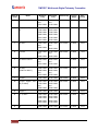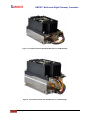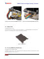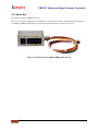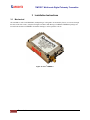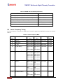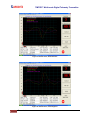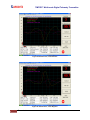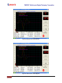
1
ISO 9001:2008 Certified TIMTERTM T3 Multi-mode Digital Telemetry Transmitter Installation and Operation Manual Quasonix, Inc. 6025 Schumacher Park Dr. West Chester, OH 45069 20 October 2015 Revision 3.2.7 Specifications subject to change without notice. Approved for Public Release 15-S-2138 No part of the document may be circulated, quoted, or reproduced for distribution without prior written approval from Quasonix, Inc. Copyright Quasonix, Inc., All Rights Reserved. TIMTER™ Multi-mode Digital Telemetry Transmitter Table of Contents 1 Introduction ............................................................................................................................................ 1 1.1 Description ................................................................................................................................... 1 1.2 Nomenclature .............................................................................................................................. 1 1.3 Part Number Field Codes ............................................................................................................ 3 1.3.1 Frequency Bands .................................................................................................................... 3 1.3.2 Clock and Data Interface ......................................................................................................... 5 1.3.3 Serial Control Interface............................................................................................................ 6 1.3.4 ARTM Tier 0 (PCM/FM)........................................................................................................... 6 1.3.5 ARTM Tier I (SOQPSK-TG) .................................................................................................... 6 1.3.6 ARTM Tier II (Multi-h CPM) ..................................................................................................... 6 1.3.7 Legacy ..................................................................................................................................... 7 1.3.8 RF Output Power..................................................................................................................... 7 1.3.9 Packages................................................................................................................................. 7 1.3.10 Automatic Carrier Wave Output Option - AC ...................................................................... 8 1.3.11 Auxiliary Input Option – AI .................................................................................................. 8 1.3.12 Adapter Plate – AP.............................................................................................................. 9 1.3.13 Baud Rate Option – BRx..................................................................................................... 9 1.3.14 CP07 Control Protocol Option – C7 .................................................................................... 9 1.3.15 Convolutional Encoder Option – K7 (formerly CE option) .................................................. 9 1.3.16 Clock-free Baseband Interface Option – CF..................................................................... 10 1.3.17 Clock Generator Output Option – CG ............................................................................... 11 1.3.18 Dual Power Option – DP................................................................................................... 11 1.3.19 Ethernet Payload Capability – EN..................................................................................... 11 1.3.20 Analog Frequency Modulation – FM ................................................................................. 11 1.3.20.1 Using True Analog FM.................................................................................................. 11 1.3.21 Frequency Offset – FO ..................................................................................................... 12 1.3.22 GPS Notch Option – GN ................................................................................................... 12 1.3.23 High Bit Rate Option – HR ................................................................................................ 12 1.3.24 Internal Clock and Data Option – ID ................................................................................. 12 1.3.25 Limited Current Option - LC .............................................................................................. 12 1.3.26 Forward Error Correction / Low Density Parity Check (LDPC) Option – LD..................... 13 1.3.27 Low Bit Rate Option – LR ................................................................................................. 13 1.3.28 Randomizer Control Option – MK ..................................................................................... 13 1.3.29 Modulation Scaling Option – MS....................................................................................... 13 1.3.30 MDM-9 Accessory Board – P9.......................................................................................... 13 i Quasonix, Inc. TIMTER™ Multi-mode Digital Telemetry Transmitter 2 3 4 1.3.31 Parallel Port Frequency Programming Option – PF ......................................................... 13 1.3.32 Parallel Port Mode Selection Option – PM ....................................................................... 13 1.3.33 Hardware Preset Option – PS (PS2, PS4, PS8, or PS16)................................................ 13 1.3.34 Recall Holdoff Option – RH............................................................................................... 13 1.3.35 Randomizer Output Option – RN ...................................................................................... 14 1.3.36 Spacecraft Tracking and Data Network Option – STDN................................................... 14 1.3.37 Switch Box Option – SWBX .............................................................................................. 14 1.3.38 Variable FIFO Depth Option – VF..................................................................................... 14 1.3.39 Variable Power Option – VP ............................................................................................. 14 1.3.40 Wide Input Voltage Range Option – WV........................................................................... 14 Accessories.......................................................................................................................................... 15 2.1 Fan-cooled Heat Sink ................................................................................................................ 15 2.2 Transmitter-powered Heat Sink ................................................................................................. 16 2.3 Adapter Plate ............................................................................................................................. 18 2.4 Pre-wired MDM-15 for RS-422 Units......................................................................................... 18 2.5 Pre-wired MDM-15 for TTL Units............................................................................................... 19 2.6 MDM-15 Wiring Harness for RS-422 Units................................................................................ 19 2.7 MDM-15 Wiring Harness for TTL Units ..................................................................................... 20 2.8 Ruggedized Handheld Programmer .......................................................................................... 20 2.9 USB to Serial Converter Cable .................................................................................................. 21 2.10 Switch Box ................................................................................................................................. 22 Installation Instructions ........................................................................................................................ 23 3.1 Mechanical................................................................................................................................. 23 3.2 Thermal...................................................................................................................................... 25 3.3 Electrical .................................................................................................................................... 25 Operating Instructions.......................................................................................................................... 28 4.1 Power-on Operation................................................................................................................... 28 4.1.1 4.2 Dual Power via Hardware Control ......................................................................................... 28 TIMTER™ Serial Control Protocol............................................................................................. 28 4.2.1 Command Set: Standard and Optional Commands.............................................................. 29 4.2.1.1 5 4.2.1.1.1 Input Source Selection Command - IS.................................................................... 49 4.2.1.1.2 System Status Command – SY............................................................................... 52 RF Output Notes .................................................................................................................................. 54 5.1 6 Additional Command Set Details.................................................................................. 49 Troubleshooting the RF on a Quasonix Transmitter ................................................................. 54 Performance Specifications ................................................................................................................. 57 6.1 RF Output .................................................................................................................................. 57 ii Quasonix, Inc. TIMTER™ Multi-mode Digital Telemetry Transmitter 6.2 Electrical Current ....................................................................................................................... 57 6.3 Environmental Specifications .................................................................................................... 57 6.4 Carrier Frequency Tuning.......................................................................................................... 58 6.5 Carrier Frequency Error............................................................................................................. 59 6.6 Bit Error Rate ............................................................................................................................. 59 6.7 Modulated RF Power Spectrum ................................................................................................ 60 6.8 Phase Noise Power Spectrum................................................................................................... 62 6.9 Baseplate Temperature ............................................................................................................. 63 6.10 Vibration and Shock................................................................................................................... 63 6.10.1 Vibration Testing ............................................................................................................... 65 6.10.2 Shock Testing ................................................................................................................... 68 7 Maintenance Instructions..................................................................................................................... 72 8 Product Warranty ................................................................................................................................. 73 9 Technical Support and RMA Requests ............................................................................................... 74 10 Appendix A – Preset Option............................................................................................................. 75 11 Appendix B – Acronym List .............................................................................................................. 76 List of Figures Figure 1: Quasonix Part Number Construction Description.......................................................................... 1 Figure 2: FPCM Signal on Oscilloscope ....................................................................................................... 8 Figure 3: CCSDS 131.0-B-1 Rendering of Basic Convolutional Encoder Diagram.................................... 10 Figure 4: Fan-cooled Heat Sink and Power Supply.................................................................................... 15 Figure 5: Fan-cooled Heat Sink with 6 cubic inch TIMTER™..................................................................... 15 Figure 6: Transmitter-powered Heat Sink and Pigtail Cable....................................................................... 16 Figure 7: Transmitter-powered Heat Sink Mounted on an 04AB Package................................................. 17 Figure 8: Transmitter-powered Heat Sink Mounted on a 07AE Package................................................... 17 Figure 9: Close-up Using Female MDM-15 Connector............................................................................... 18 Figure 10: Close-up Using Male MDM-15 Connector................................................................................. 18 Figure 11: Adapter Plate ............................................................................................................................. 18 Figure 12: Pre-wired MDM-15 with 36” Pigtails for RS-422........................................................................ 19 Figure 13: Pre-wired MDM-15 with 36” Pigtails for TTL.............................................................................. 19 Figure 14: MDM-15 Cable Harness for RS-422.......................................................................................... 20 Figure 15: MDM-15 Cable Harness for TTL................................................................................................ 20 Figure 16: Ruggedized Handheld Programmer .......................................................................................... 21 iii Quasonix, Inc. TIMTER™ Multi-mode Digital Telemetry Transmitter Figure 17: USB to Serial Converter Cable .................................................................................................. 21 Figure 18: Switch Box with 36” MDM-9 to MDM-9 Cable Harness............................................................. 22 Figure 19: 4.2 in3 TIMTER™.......................................................................................................................23 Figure 20: Outline Drawing, TIMTER™ 04AB Telemetry Transmitter ........................................................ 24 Figure 21: MDM-15 Female Pin Numbering, RS-422 Interface – 04AB Package...................................... 26 Figure 22: MDM-15 Male Pin Numbering, TTL Interface – 04AD Package................................................ 26 Figure 23: Baseband Signal Timing............................................................................................................ 27 Figure 24: TIMTER™ Welcome Message .................................................................................................. 29 Figure 25: PCM/FM (Tier 0) Power Spectral Density with Mask ................................................................ 61 Figure 26: SOQPSK-TG (Tier I) Power Spectral Density with Mask .......................................................... 61 Figure 27: MULTI-h CPM (Tier II) Power Spectral Density with Mask ....................................................... 62 Figure 28: Phase Noise Limit Curve ........................................................................................................... 63 Figure 29: Vibration / Shock Testing System.............................................................................................. 64 Figure 30: TIMTER™ Mounted for Z-axis Testing ...................................................................................... 64 Figure 31: TIMTER™ Mounted for X-axis Testing...................................................................................... 65 Figure 32: TIMTER™ Mounted for Y-axis Testing...................................................................................... 65 Figure 33: TIMTER™ Vibration Profile ....................................................................................................... 66 Figure 34: Z-axis Vibration Spectrum ......................................................................................................... 67 Figure 35: Y-axis Vibration Spectrum ......................................................................................................... 67 Figure 36: X-axis Vibration Spectrum ......................................................................................................... 68 Figure 37: Shock Pulse, Z-axis Positive ..................................................................................................... 69 Figure 38: Shock Pulse, Z-axis Negative.................................................................................................... 69 Figure 39: Shock Pulse, Y-axis Positive ..................................................................................................... 70 Figure 40: Shock Pulse, Y-axis Negative.................................................................................................... 70 Figure 41: Shock Pulse, X-axis Positive ..................................................................................................... 71 Figure 42: Shock Pulse, X-axis Negative.................................................................................................... 71 List of Tables Table 1: Model Configuration Example......................................................................................................... 3 Table 2: Frequency Band Codes .................................................................................................................. 3 Table 3: Clock and Data Interface Codes ..................................................................................................... 5 Table 4: Serial Control Interface Codes........................................................................................................ 6 Table 5: ARTM Tier 0 Codes ........................................................................................................................ 6 Table 6: ARTM Tier I Codes ......................................................................................................................... 6 iv Quasonix, Inc. TIMTER™ Multi-mode Digital Telemetry Transmitter Table 7: ARTM Tier II Codes ........................................................................................................................ 7 Table 8: Legacy Codes ................................................................................................................................. 7 Table 9: RF Output Power Codes................................................................................................................. 7 Table 10: Package Codes............................................................................................................................. 8 Table 11: Standard Bit Rates Compared to Low/High Rate Options.......................................................... 12 Table 12: Standard and Optional User Commands.................................................................................... 30 Table 13: DC Input Current at Standard Input Voltage............................................................................... 57 Table 14: TIMTER™ Environmental Specifications.................................................................................... 58 Table 15: Carrier Frequencies (MHz) ......................................................................................................... 58 Table 16: Transmitter BER Specifications with Quasonix Demodulator..................................................... 60 Table 17: K and m Values per Waveform ................................................................................................... 60 Table 18: Random Vibration Spectrum....................................................................................................... 66 v Quasonix, Inc. TIMTER™ Multi-mode Digital Telemetry Transmitter 1 Introduction 1.1 Description This document describes the Installation and Operation of Quasonix’ TIMTERTM T3 Multi- mode Digital Telemetry Transmitters. The transmitters are designed to transmit airborne telemetry data from a test article to ground stations. The transmitters are developed, manufactured, and supported by: Quasonix, Inc. 6025 Schumacher Park Drive West Chester, OH 45069 CAGE code: 3CJA9 1.2 Nomenclature The earliest models of these transmitters were referred to as Tier I Missile Test Transmitters (TIMTER™) because they were intended for missiles and offered only ARTM Tier I (SOQPSK) modulation. Although the model line now includes much more than ARTM Tier I, and they are in widespread use on many platforms besides missiles, the “TIMTER” name remains. Now in its third generation and commonly referred to as TIMTER™ 3, the transmitter is available in a number of variations, depending on the options specified at the time of order. The type of features and modes installed in each unit are identified in the model number, as depicted in Figure 1. Package field codes are listed in Table 10. For questions about specific packages, please contact Quasonix. Transmitter Part Numbering Example QSX-V S B 2 - 1 1 1 0 - 05 - 04 - 04AB - CF Legacy Serial Control Interface 2 = RS-232 T= TTL ARTM CPM Clock and Data Interface code (refer to page 4 for list) SOQPSK‐TG Frequency Band Code (refer to page 2 for list) PCM/FM Standard Prefix Mode: 1= Enabled 0=Not enabled Options, separated by hyphens (example clock free) Package Code (refer to page 3) Pinout Code (Contact Quasonix) Power Code (refer to table this page) Figure 1: Quasonix Part Number Construction Description In this manual, the words Terminal Control and Serial Control have the same meaning and are used synonymously throughout this manual. Serial control originates from configuring the transmitter from a computer's legacy RS232/422 serial communications (COM) port. Terminal Control reflects the more generic case where the transmitter could be controlled by other standard computer interfaces such as Ethernet. 1 Quasonix, Inc. TIMTER™ Multi-mode Digital Telemetry Transmitter The nanoTX transmitter models are covered in a separate user manual, available for download from the company website: www.quasonix.com. The available TIMTER™ software and hardware options are listed below. Refer to section 1.3 for detailed descriptions of each option. 2 AC Automatic carrier wave output AI Auxiliary Input for digital data that is already premod filtered AP Adapter plate for 2.5”x 3.5” footprint – Include this hardware accessory with order BRx Request non standard baud rate for serial control C7 IRIG 106 Appendix N serial control protocol CF Clock-free baseband interface CG Clock generator output to baseband connector DP Dual power (Ability to set a low and a high setting, hardware controlled*) EN Ethernet Payload Capability FM Allows the TIMTER™ to function as an analog FM transmitter FO Frequency Offset GN GPS notch filters to meet 115 dBm in 3 kHz band at L1 and L2 (S band only) – Include this hardware option with order HR Increases max bit rate up to 46 Mbps (23 Mbps for PCM/FM) (20 Mbps max for Clock Free mode) ID Internal Clock and Data can be saved as a power-up default K7 Convolutional encoder (includes NRZ-M encoding) (k=7 rate 1/2) LC Low current in the RF Off state, 10 mA (hardware option) LD LDPC forward error correction encoding LR Decreases min bit rate to 50 kbps (25 kbps for PCM/FM) (50 kbps min for Clock Free mode) MK Randomizer hardware control – Include this hardware option with order MS Modulation scaling P9 MDM-9 Accessory board (use with switch box part QSX-AC-SWBX-P9-3B-3M) PF Parallel port frequency programming PM Parallel port mode selection PS Enable hardware presets (specify 2, 4, 8, or 16 – PS2, PS4, PS8, PS16) RH Recall Holdoff RN Randomizer output to baseband connector STDN Supports Spacecraft Tracking and Data Network (PM/BPSK) mode SWBX Includes switch box and 36” MDM-9 to MDM-9 cable harness (For use with P9 option) VF Variable FIFO Depth, controls transmitter latency Quasonix, Inc. TIMTER™ Multi-mode Digital Telemetry Transmitter VP Variable power (31 settings, spanning 24 dB), software controlled* WV Wide input voltage range Refer to Table 12 in section 4.2.1 for detailed descriptions of each option. Due to input connector pin count limitations, certain combinations of options are not available. Please contact Quasonix for support in ordering TIMTER™ options or for information regarding upgrades to TIMTER™ units that you may already own. The model number identifies the configuration of the unit. For example, model number QSX-VSTT-1100-10-0404AB-CF defines a unit configured as shown in Table 1. Table 1: Model Configuration Example Identifiers 1.3 Description QSX Quasonix product V Variable bit rate S S band code T TTL clock and data interface code 2 RS-232 serial control interface: baud rate 57,600 1100 Tier 0 present, Tier I present, Tier II absent, Legacy absent 10 10 Watt RF output 04 Pinout code 04 04AB Package code CF Clock-free baseband interface option Part Number Field Codes 1.3.1 Frequency Bands Frequency band codes are listed in Table 2. Table 2: Frequency Band Codes Band ID Code Band Minimum Freq Maximum Freq Default Freq 2250.5 MHz A Lower S 2200.5 MHz 2300.5 MHz B Euro Mid C 5091.0 MHz 5250.0 MHz C C “Low” 4400.0 MHz 4950.0 MHz 3 Quasonix, Inc. 4620.0 MHz Tuning Steps Max Power 0.5 MHz 25 W 0.5 MHz 20 W 0.5 MHz 20 W TIMTER™ Multi-mode Digital Telemetry Transmitter Band ID Code D Band Minimum Freq Maximum Freq Default Freq 4400.0 MHz and 4950.0 MHz and 5120.0 MHz 0.5 MHz 20 W 5091.0 MHz 5150.0 MHz 1435.5 MHz 1750.0 MHz 2200.5 MHz 1534.5 MHz 1855.0 MHz 2394.5 MHz 1450.5 MHz 0.5 MHz 10 mW 4400.0 MHz 4950.0 MHz 5091.0 MHz 5150.0 MHz 5091.0 MHz 5250.0 MHz 2200.5 MHz and 2394.5 MHz 2370.5 MHz 0.5 MHz 20 W 4400.0 MHz 4950.0 MHz 1435.5 MHz and 1534.5 MHz and 1450.5 MHz 0.5 MHz 10 W 4400.0 MHz 4950.0 MHz 4400.0 MHz 4950.0 MHz 0.5 MHz 20 W and and 5091.0 MHz 5250.0 MHz S and C 2200.5 MHz 2394.5 MHz 2370.5 MHz 0.5 MHz 20/18 W (with Euro Mid C) 4400.0 MHz and 4950.0 MHz and 5091.0 MHz 5250.0 MHz C (with Mid C) E L, S, C, and Euro Mid C F S and C H L and C J C and Euro Mid C K Tuning Steps Max Power and L Lower L 1435.5 MHz 1534.5 MHz 1450.5 MHz 0.5 MHz 20 W M Lower L, Upper L, and S (Tri-band) 1435.5 MHz 1750.0 MHz and 1534.5 MHz 1855.0 MHz and 1450.5 MHz 0.5 MHz 20 W 2200.5 MHz 2394.5 MHz 0.5 MHz 25 W 1450.5 MHz 0.5 MHz 10 W 2370.5 MHz 0.5 MHz 25 W N Upper S 2300.5 MHz 2394.5 MHz Q L, S, and C 1435.5 MHz 1750.0 MHz 2200.5 MHz 1534.5 MHz 1855.0 MHz 2394.5 MHz 4400.0 MHz 5091.0 MHz 4950.0 MHz 5150.0 MHz 2200.5 MHz 2394.5 MHz S S 4 Quasonix, Inc. TIMTER™ Multi-mode Digital Telemetry Transmitter Band ID Code T Band Lower L and C Minimum Freq Maximum Freq Default Freq Tuning Steps Max Power 1435.5 MHz 1534.5 MHz 1450.5 MHz 0.5 MHz 10 W 4400.0 MHz 4950.0 MHz 5091.0 MHz 5150.0 MHz 5091.0 MHz 5250.0 MHz U Upper L 1750.0 MHz 1855.0 MHz 1800.5 MHz 0.5 MHz 20 W V S and C 2200.5 MHz 2394.5 MHz 2370.5 MHz 0.5 MHz 20 W (with Mid C) 4400.0 MHz and 4950.0 MHz and 5091.0 MHz 5150.0 MHz S and C 2200.5 MHz 2394.5 MHz 2370.5 MHz 0.5 MHz 20 W (with Euro Mid C) 4400.0 MHz and 4950.0 MHz and 5091.0 MHz 5250.0 MHz W 1.3.2 Clock and Data Interface Clock and data interface codes are listed in Table 3. Table 3: Clock and Data Interface Codes Clock and Data Interface Code 5 Baseband Clock and Data Interface A TTL; Selectable between 75 ohms to ground and 10k ohms to ground B RS-422 (120 ohms differential, even when unit is powered off) D Dual-mode; Selectable between TTL (terminated 75 ohms to ground) and RS-422 (terminated 120 ohms differential) H TTL (10k ohms to ground) L LVDS (Low Voltage Differential Signal) M Dual-mode; Selectable between TTL (terminated 10 ohms to ground) and RS-422 (terminated 120 ohms differential) R RS-422 (120 ohms differential) S Tri-mode; Selectable between TTL (terminated 75 ohms to ground), TTL (terminated 10k ohms to ground), and RS-422 (terminated 120 ohms differential) T TTL (75 ohms to ground) Quasonix, Inc. TIMTER™ Multi-mode Digital Telemetry Transmitter 1.3.3 Serial Control Interface Serial control interface codes are listed in Table 3. Table 4: Serial Control Interface Codes Serial Control Interface Code 1.3.4 Serial Control Interface 1 LVTTL; 57,600 baud rate 2 RS-232; 57,600 baud rate T TTL; 57,600 baud rate 4 RS-422; 57,600 baud rate D Dual-mode, software selectable between RS-232 or RS-422; 57,600 baud rate ARTM Tier 0 (PCM/FM) ARTM Tier 0 codes are listed in Table 5. Table 5: ARTM Tier 0 Codes 1.3.5 Part Number Code PCM/FM (ARTM Tier 0) 0 Absent 1 Present ARTM Tier I (SOQPSK-TG) ARTM Tier I codes are listed in Table 6. Table 6: ARTM Tier I Codes 1.3.6 Part Number Code SOQPSK-TG (ARTM Tier I) 0 Absent 1 Present ARTM Tier II (Multi-h CPM) ARTM Tier II codes are listed in Table 7. 6 Quasonix, Inc. TIMTER™ Multi-mode Digital Telemetry Transmitter Table 7: ARTM Tier II Codes 1.3.7 Part Number Code Multi-h CPM (ARTM Tier II) 0 Absent 1 Present Legacy Legacy modes include BPSK, QPSK, and OQPSK. Legacy codes are listed in Table 7. Table 8: Legacy Codes 1.3.8 Part Number Code Legacy Modes 0 Absent 1 Present RF Output Power RF output power codes are listed in Table 9. Table 9: RF Output Power Codes Part Number Code 00 RF Output Power 10 mW (+10 dBm), ±1 dB for single band 20 mW (+13 dBm), ±1 dB for tri band Requires DC input of 6.5 V, unless “WV” option is specified 1.3.9 01 1 watt (+30 dBm), minimum 02 2 watt (+33 dBm), minimum 05 5 watts (+37 dBm), minimum 10 10 watts (+40 dBm), minimum 20 20 watts (+43 dBm), minimum 25 25 watts (+44 dBm), minimum Packages Package field codes are listed in Table 10. Detailed information for packages other than 04AB is located in the TIMTER™ Transmitter Packages document, available at the Quasonix web site. For questions about specific packages, please contact Quasonix. 7 Quasonix, Inc. TIMTER™ Multi-mode Digital Telemetry Transmitter Table 10: Package Codes TIMTER™ Package Width Length 02XX 1.992 in 3 2.000” 3.000” 0.332” 04XX 4.200 in3 2.000” 3.000” 0.700” 05XX 4.800 in3 2.000” 3.000” 0.800” 06XX 6.072 in3 2.000” 3.000” 1.012” 07XX 6.546 in3 2.000” 3.000” 1.091” 6.672 in3 2.000” 3.000” 1.112” 7.590 in3 2.200” 3.450” 1.000” 8.418 in3 2.000” 3.450” 1.403” 14XX 14.105 in3 2.500” 3.500” 1.612” 17XX, with heat sink 18.760 in3 2.500” 3.500” 2.144” 08XX Volume Height *Package dimensions do not include connectors Transmitter weight may vary depending on packages and applications. For information about the weight of a particular transmitter, please contact Quasonix. 1.3.10 Automatic Carrier Wave Output Option - AC This option allows the TIMTER to transmit a carrier wave when the clock input is absent, which would normally cause the RF output to be turned off. 1.3.11 Auxiliary Input Option – AI The AI option provides an auxiliary input that allows the TIMTER™ to transmit Filtered PCM (FPCM) data. FPCM is a binary data waveform that has been filtered such that the data transitions are slowed down. The FPCM signal at the TIMTER, viewed on an oscilloscope, might look something like the following figure. Figure 2: FPCM Signal on Oscilloscope The AI option allows the TIMTER™ to replace a legacy analog transmitter, but only for use in transmitting a digital data stream. Refer to the FM option in section 1.3.21 for configuring the TIMTER™ to transmit a true analog signal, such as NTSC video. The AI option is frequently used to interface the TIMTER™ to legacy encryption 8 Quasonix, Inc. TIMTER™ Multi-mode Digital Telemetry Transmitter devices, which often include filtering on their outputs, including a DC blocking capacitor. By default, the Auxiliary Input is configured to accept an AC-coupled input. The AIR command may be used to select between a zero and a non-zero DC bias. The auxiliary input converts the FPCM input back to an unfiltered bit stream, locks an internal bit sync to that bit stream (refer to the CF option), and then modulates the transmitter based on that digital bit stream, in which case the deviation and the internal premod filter bandwidth are set by the bit rate, and are independent of the analog voltage levels presented to the transmitter. Use of the auxiliary input requires the –AI option. The command for controlling auxiliary input is AI, which enables/disables the auxiliary input (when disabled, the normal digital input is used). Since there is no clock input, the Clock Free option (CF) is required. (Refer to section 1.3.15 for more information about Clock Free.) To configure the TIMTER™ for use with the Auxiliary Input, issue the following commands: AI = 1 (get data stream from Auxiliary Input) CF = 0 (operate clock free) BR xxx, where xxx = data rate in Mbps, or BR A for automatic data rate AIR x, where x = 0 for zero DC bias and x = 1 for 1.65V DC bias 1.3.12 Adapter Plate – AP Use this option to include the 2.5” x 3.5” adapter plate (hardware accessory) with the order. 1.3.13 Baud Rate Option – BRx The BR option changes the serial communications default baud rate on the transmitter to the one selected. A number from 0-7 follows the BR option request. Corresponding values are as follows: 0 = 57600; 1 = 4800; 2 = 9600; 3 = 19200; 4 = 38400; 5 = 56000; 6 = 57600; 7 = 115200. 1.3.14 CP07 Control Protocol Option – C7 The IRIG 106-07 serial control protocol (CP07), Appendix N “provides standards for commands, queries, and status information when communicating with telemetry transmitters configured with communication ports.” The Basic command set contains the minimum (required) commands for transmitter control, query, and status. The Extended command set contains optional commands that may or may not be implemented at the manufacturer’s discretion. CP07 is enabled when the C7 option is requested. The default baud rate for CP07 transmitters is 9600. 1.3.15 Convolutional Encoder Option – K7 (formerly CE option) The K7 option enables convolutional encoding and NRZ-M conversion. This encoding adds redundant information to the transmitted data stream to help detect and correct bit errors that may occur, particularly due to predominantly Gaussian noise. Use of convolutional encoding requires a matching Viterbi decoder in the receiver to extract the source data. The encoded data rate will be twice the source data rate, and the occupied bandwidth will also be doubled. For example, the transmitter has two encoders, one for in-phase (“I”) data and one for quadrature (“Q”) data. Call the input symbol stream I0/Q0, I1/Q1, … . Each encoder outputs 2 bits for every input bit, so call the output bit stream from the first convolutional encoder I0(1), I0(2), I1(1), I1(2), … , and call the output bit stream from the second convolutional encoder Q0(1), Q0(2), Q1(1), Q1(2), … . Combining the outputs of the two encoders, then, the output symbol stream is I0(1)/Q0(1), I0(2)/Q0(2), I1(1)/Q1(1), I1(2)/Q1(2), … . For modes that do not employ Quadrature modulation, such as PCM/FM, Multi-h CPM, and BPSK, only a single encoder is used. 9 Quasonix, Inc. TIMTER™ Multi-mode Digital Telemetry Transmitter A single encoder is implemented exactly as described in the “Consultative Committee for Space Data Systems, Recommendation for Space Data System Standards, TM Synchronization and Channel Coding, CCSDS 131.0-B-1, Blue Book, September 2003, Section 3.” A basic convolutional encoder block diagram, as illustrated in CCSDS 131.0-B1, is shown in Figure 3. Figure 3: CCSDS 131.0-B-1 Rendering of Basic Convolutional Encoder Diagram 1.3.16 Clock-free Baseband Interface Option – CF Clock-free is an optional mode that transmits user data, but uses an internal bit sync to take the place of the normal external clock. The standard TIMTER requires external clock and data inputs. With the CF option, no external clock is required. The clock is generated directly from the data and a user-specified bit rate. Because the internal bit sync’s clock takes the place of the normal external clock in clock-free mode, the selected clock source must be external for clock-free just like it is for normal clock/data. This mode is most often use to retrofit older analog transmitters in TM systems where the crypto does not deliver a clock to the transmitter. The commanded clock-free rate can be saved, and it will be restored at power-on. When the CF option is used, the bit rate range is 0.1 to 35 Mbps for all waveform modes. It is limited by the bit rate achievable for the current mode. (Refer also to the HR and LR options for extended bit rates, and the ID option for Internal Clock and Data.) Do not confuse the CF option with CS/DS commands. 10 Quasonix, Inc. TIMTER™ Multi-mode Digital Telemetry Transmitter Internal clock (CS 1 Command) is used when the transmitter is to be a test source only. The unit transmits the selected internal data pattern (DS 1 command) at the bit rate set by the user via the IC command. The internal clock is not used to transmit actual payload data. External clock (CS 0 Command) is the normal mode: the user supplies clock and data. Refer to Table 12 for user commands. 1.3.17 Clock Generator Output Option – CG The standard TIMTER includes internal clock and data generators, generally used for system test. The CG option brings this internal clock out of the unit on the primary MDM-15 connector. The assignment of output pins depends on the other features selected. Consult Quasonix to order the CG option. 1.3.18 Dual Power Option – DP The standard TIMTER operates at its full rated RF output power. The DP option provides two softwareprogrammed, hardware-actuated settings, designated by the user as “high power” and “low power”. There are 32 choices for “high power” and 32 choices for “low power”. The low power setting can provide as much as 24 dB of attenuation from the high power setting. 1.3.19 Ethernet Payload Capability – EN The -EN option gives the transmitter the ability to send Ethernet data via direct connection to a standard Ethernet network. Operating in Ethernet mode, the user sets the desired transmission rate through the transmitter control interface. As Ethernet data are presented to the TIMTER, they are loaded into a large transmit buffer. If the presented Ethernet traffic does not keep the buffer filled, bit stuffing is used to attain the programmed transmit rate. If the presented traffic overflows the buffer, Ethernet data are discarded. The Ethernet interface is supported via an MDM-9 connector, and is compatible with 10Base-T and 100Base-TX Ethernet physical layers. The maximum transmission rate is 46 Mbps. Use of a transmitter with the -EN option requires a Quasonix RDMS™ receiver to reconstruct the Ethernet data at the receive end. 1.3.20 Analog Frequency Modulation – FM This option allows the TIMTER™ to function as an analog FM transmitter. In this mode, the analog input voltage is converted to frequency offset, relative to the carrier, based on a settable deviation scale factor. No filtering or other signal processing is performed, and commands and functions related to digital clock/data do not affect the modulated output. This mode of operation is designed for use with a true analog signal, such as NTSC video. By default, the analog FM input is AC coupled, with a low frequency cutoff of less than 15 Hz. Contact Quasonix if you need a DC coupled analog input. FM mode is not optimal for sending digital data; refer to the AI option in section 1.3.11 for that configuration. However, if your TIMTER™ has only the FM option, and not the AI option, you can still use it to transmit digital data, but you will not have the greatest benefit of the AI option: the internal bit sync is not available to set the internal premod filter and deviation automatically. When using the FM mode to send digital data, the premod filtering must be performed externally, and the deviation is set using the AFMS command (refer to section 1.3.20.1). 1.3.20.1 Using True Analog FM Analog FM provides the capability of frequency modulating the RF carrier based on an analog input signal voltage, making the Quasonix digital transmitter behave virtually identically to an analog PCM/FM transmitter (but with improved phase noise, more precise deviation control, etc.). Analog FM requires the –FM option. The two commands for controlling analog FM are MO and AFMS. MO 12 enables the analog FM input, and AFMS sets the sets the deviation in MHz per Volt. (Refer to the Command Set section 4.2.1, for specific information about each command.) In order to use TRUE analog FM: 11 Quasonix, Inc. TIMTER™ Multi-mode Digital Telemetry Transmitter The -FM option must be in the part number Mode must be set to MO 12 Use AFMS xx command to set the deviation sensitivity to xx MHz / volt; for example AFMS 1.0 Refer also to the Auxiliary Input option, section 1.3.11. 1.3.21 Frequency Offset – FO This option is used to set frequencies that are NOT aligned to the synthesizer step size for their units, typically 500 kHz, and it enables the FO user command. 1.3.22 GPS Notch Option – GN Use this option to specify GPS notch filters to meet 115 dBm in 3 kHz band at L1 and L2 (hardware note). Available for S band only. Consult Quasonix for pricing and availability. 1.3.23 High Bit Rate Option – HR The standard TIMTER supports bit rates from 0.1 to 28 Mbps in SOQPSK-TG and MULTI-h CPM modes, 0.05 to 14 Mbps in PCM/FM (Tier 0) mode and in all legacy modes. The HR option increases the bit rate to a maximum of 46 Mbps (23 Mbps for PCM/FM). (The maximum bit rate with a Clock Free transmitter is 35 Mbps for SOQPSKTG and MULTI-h CPM modes; 23 Mbps for PCM/FM and all legacy modes.) Refer to the CF option for information about the Clock Free option. Refer to Table 11 for bit rate comparisons by mode. Table 11: Standard Bit Rates Compared to Low/High Rate Options Standard Bit Rate With Low Rate Option -LR With High Rate Option -HR ARTM Tier 0 Modulation (PCM/FM) 0.05 -14 Mbps Down to 0.025 Mbps Up to 23 Mbps ARTM Tier I Modulation (SOQPSK-TG) 01 - 28 Mbps Down to 0.050 Mbps Up to 46 Mbps ARTM Tier II Modulation (Multi-h CPM) 01 - 28 Mbps Down to 0.050 Mbps Up to 36 Mbps Legacy Modulation (BPSK) 0.05 - 10 Mbps N/A N/A Legacy (QPSK, OQPSK) 0.05 - 20 Mbps N/A N/A 1.3.24 Internal Clock and Data Option – ID The ID option allows the CS and DS user settings to be reloaded on power up or on a manual recall of a setup. Without the ID option, CS and DS are both forced to 0. Refer to the CF option for information about the Clock Free option. 1.3.25 Limited Current Option - LC This option is used to specify low current in the RF Off state. Current draw is less than 10 mA when the transmitter is Off. This is a hardware option. 12 Quasonix, Inc. TIMTER™ Multi-mode Digital Telemetry Transmitter 1.3.26 Forward Error Correction / Low Density Parity Check (LDPC) Option – LD This option provides the Low Density Parity Check (LDPC) encoding, which is being considered for use on the iNET program. LDPC has been adopted by the Range Commander’s Council, IRIG 106-15, Appendix R. 1.3.27 Low Bit Rate Option – LR The standard TIMTER™ supports bit rates from 0.1 to 28 Mbps in SOQPSK-TG and MULTI-h CPM modes, 0.05 to 14 Mbps in PCM/FM (Tier 0) mode and in all legacy modes. The LR option decreases the bit rate to a minimum of 50 kbps (25 kbps for PCM/FM). (The minimum bit rate with a Clock Free transmitter is 50 kbps for all modes.) Refer to the CF option for information about the Clock Free option. Refer to Table 11 for bit rate comparisons by mode. 1.3.28 Randomizer Control Option – MK The standard TIMTER™ provides a user command (RA) that reports or sets the randomizer state. This option enables ON/OFF control of the randomizer with a hardware pin. Use this option to specify the Randomizer Control (hardware configuration) with the order. 1.3.29 Modulation Scaling Option – MS This option enables the MS and MJ commands which allow a user to set the modulation scaling factor and scale the modulation index of the transmitted signal. For additional information, refer to Table 12, or contact Quasonix. 1.3.30 MDM-9 Accessory Board – P9 Use this option to include the MDM-9 Accessory Board (sometimes referred to as a “tophat board”) (hardware accessory), for use with switch box part number QSX-AC-SWBX-P9-3B-3M, with the order. 1.3.31 Parallel Port Frequency Programming Option – PF This option adds a parallel port in the form of an MDM-15 connector for manual frequency tuning. The PF option requires the addition of a Quasonix MDM-9 Accessory Board. Consult Quasonix to order the PF option. 1.3.32 Parallel Port Mode Selection Option – PM This option adds a parallel port in the form of an MDM-15 connector for manual mode selection. The PM option requires the addition of a Quasonix MDM-9 Accessory Board. Consult Quasonix to order the PM option. 1.3.33 Hardware Preset Option – PS (PS2, PS4, PS8, or PS16) The TIMTER™ supports one or more hardware presets. A single preset defines the complete state of the transmitter, including carrier frequency, modulation mode, data polarity, randomizer state, etc. Without the PS option, the TIMTER™ supports only one hardware preset, which it reverts to at power-up. The PS in the option string specifies that the unit supports multiple hardware presets (2, 4, 8, or 16). Presets are engaged by grounding various combinations of pins on the terminal/parallel control selection. The number of presets available and which pins engage the presets depend on the other features specified. Due to the limited number of pins available, the PS option may require the elimination of the RF On/Off pin. Due to firmware part number parsing requirements, the hardware preset option code must be at the very end of the part number to be valid. On units which use the standard MDM-15 connector, the ZY command displays the connector pinout showing preset pin locations. 1.3.34 Recall Holdoff Option – RH If the RF On/Off pin is grounded on power up, then the RF command is set to RF 0 (OFF) regardless of how the command was saved. The user must send the RF On/Off command via serial port to enable RF output. Otherwise, if RF 1 (ON), and the RF On/Off pin is active (based on the RZ command setting), and the unit has a clock (non clock free, non AC unit), then the RF output is set to ON. 13 Quasonix, Inc. TIMTER™ Multi-mode Digital Telemetry Transmitter 1.3.35 Randomizer Output Option – RN The standard TIMER includes the IRIG-106 randomizer for the RF output. The IRIG-106 randomizer is controlled through the serial interface. The RN option brings the randomized data out on the primary MDM-15 connector. The assignment of output pins depends on the other features selected. Consult Quasonix for details. 1.3.36 Spacecraft Tracking and Data Network Option – STDN This option supports the PM/BPSK mode (Spacecraft Tracking and Data Network mode). 1.3.37 Switch Box Option – SWBX The TIMTER™ provides a standard configuration interface that is easily accessible via a computer terminal. Some users prefer configuration via an external switchbox. Use this option to include a switch box and 36” MDM-9 to MDM-9 cable harness (hardware accessory option) with the order. (For use with the P9 option) 1.3.38 Variable FIFO Depth Option – VF This option enables the VF command which allows the user to set the FIFO depth on the transmitter for controlling latency time between bits in and bits out. The range is 0 to 255 with 128 being the default. If no value is entered, the current value displays. 1.3.39 Variable Power Option – VP The standard TIMTER™ operates at its full rated RF output power. The software-based VP option provides 32 discrete power level settings, spanning a range of as much as 24 dB. The steps are non-uniform, but steps are typically no larger than 1.1 dB. 1.3.40 Wide Input Voltage Range Option – WV The standard TIMTER™ operates from +28 + 4 VDC. The WV option extends operating input voltage range as shown in following table. Voltage Ranges with WV Option +6.5 to +34 VDC for 10 mWatt version +6.5 to +34 VDC for 1 Watt version +6.5 to +34 VDC for 2 Watt version +12 to +34 VDC for 5 Watt version +21 to +34 VDC for 10 Watt version +21 to +34 VDC for 20 Watt version +21 to +34 VDC for 25 Watt version Note: The WV option is not supported on 25 W S-band and 20 W S/C-band transmitters. 14 Quasonix, Inc. TIMTER™ Multi-mode Digital Telemetry Transmitter 2 Accessories Quasonix offers a number of optional accessories for TIMTER™, including a fan-cooled heat sink, a 2.5” x 3.5” adapter plate, pre-wired mating MDM-15 connectors, complete MDM-15 cable assemblies, a ruggedized handheld programmer, and a USB to serial converter cable. Contact Quasonix for pricing and availability of TIMTER™ accessories. 2.1 Fan-cooled Heat Sink Part Number: QSX-AC-32-HS-12V The heat sink assembly includes an integral +12 VDC fan and a power supply transformer, shown in Figure 4. The heat sink is shown with a mounted 6 cubic inch TIMTER™ in Figure 5. Figure 4: Fan-cooled Heat Sink and Power Supply Figure 5: Fan-cooled Heat Sink with 6 cubic inch TIMTER™ 15 Quasonix, Inc. TIMTER™ Multi-mode Digital Telemetry Transmitter 2.2 Transmitter-powered Heat Sink Part Number: (QSX-AC-32-HS-28V-SP) The heat sink assembly includes an integral +12 VDC fan, power supply, and temperature-controlled power on at +35°C. Two MDM-15 connectors and a provided pigtail cable, shown in Figure 6, allow the heat sink to draw power directly from a TIMTER™ transmitter eliminating the need for a separate external power supply. The heat sink is shown mounted on a standard 04AB TIMTER™ in Figure 7 and mounted on a larger 07AE TIMTER™ in Figure 8. The pigtail cable connects to any TIMTER™, regardless of MDM-15 gender, by plugging the pigtail into either the male or female connector, as shown in Figure 9 and Figure 10. Figure 6: Transmitter-powered Heat Sink and Pigtail Cable 16 Quasonix, Inc. TIMTER™ Multi-mode Digital Telemetry Transmitter Figure 7: Transmitter-powered Heat Sink Mounted on an 04AB Package Figure 8: Transmitter-powered Heat Sink Mounted on a 07AE Package 17 Quasonix, Inc. TIMTER™ Multi-mode Digital Telemetry Transmitter Figure 9: Close-up Using Female MDM-15 Connector 2.3 Figure 10: Close-up Using Male MDM-15 Connector Adapter Plate Part Number: QSX-AC-AP-96 The adapter plate, shown in Figure 11, allows for the standard 2” x 3” footprint TIMTER™ to be mounted to the larger 2.5” x 3.5” mounting surface occupied by other industry transmitters. Figure 11: Adapter Plate 2.4 Pre-wired MDM-15 for RS-422 Units Part Number: QSX-AC-MDM15-36-PIN An MDM-15 connector with 36” color-coded pigtail cables for connecting to transmitters with the RS-422 clock and data baseband interface is shown in Figure 12. 18 Quasonix, Inc. TIMTER™ Multi-mode Digital Telemetry Transmitter Figure 12: Pre-wired MDM-15 with 36” Pigtails for RS-422 2.5 Pre-wired MDM-15 for TTL Units Part Number: QSX-AC-MDM15-36-SOCK Quasonix offers an MDM-15 connector with 36” color-coded pigtail cables for connecting to transmitters with the TTL clock and data baseband interface. Figure 13: Pre-wired MDM-15 with 36” Pigtails for TTL 2.6 MDM-15 Wiring Harness for RS-422 Units Part Number: QSX-AC-MDM15-HARNESS-PIN An MDM-15 wiring harness for connecting to transmitters with RS-422 clock and data baseband interface is shown in Figure 14. It includes banana plugs for power and ground, BNC connectors for clock and data, and a DB-9 connector for serial control. 19 Quasonix, Inc. TIMTER™ Multi-mode Digital Telemetry Transmitter Figure 14: MDM-15 Cable Harness for RS-422 2.7 MDM-15 Wiring Harness for TTL Units Part Number: QSX-AC-MDM15-HARNESS-SOCK Quasonix offers an MDM-15 wiring harness for connecting to transmitters with TTL clock and data baseband interface. It includes banana plugs for power and ground, BNC connectors for clock and data, and a DB-9 connector for serial control. Figure 15: MDM-15 Cable Harness for TTL 2.8 Ruggedized Handheld Programmer Part Number: QSX-AC-HHPROG-800N-Y The handheld programmer is an ultra-rugged Pocket PC with custom Quasonix software that allows the user to configure transmitters through its serial interface directly in the field. The programmer is shown in Figure 16. 20 Quasonix, Inc. TIMTER™ Multi-mode Digital Telemetry Transmitter Figure 16: Ruggedized Handheld Programmer 2.9 USB to Serial Converter Cable Part Number: QSX-AC-USBSER-CONV The USB to serial converter cable allows for configuration of the transmitter with a computer that does not have a serial port. The cable is pictured in Figure 17. Figure 17: USB to Serial Converter Cable 21 Quasonix, Inc. TIMTER™ Multi-mode Digital Telemetry Transmitter 2.10 Switch Box Part Number: QSX-AC-SWBX-P9-3B-3M This accessory enables configuration of a TIMTER™ via an external switch box. Included with the switch box is a 36” MDM-9 to MDM-9 cable harness. The switch box and cable harness is pictured in Figure 18. Figure 18: Switch Box with 36” MDM-9 to MDM-9 Cable Harness 22 Quasonix, Inc. TIMTER™ Multi-mode Digital Telemetry Transmitter 3 Installation Instructions 3.1 Mechanical The standard 4.2 cubic inch TIMTER™ (04AB package) is designed to be mounted by four (4) 6-32 screws through the holes in the four corners, as depicted in Figure 20. Photos and drawings of additional TIMTER™ packages are located in the document “TIMTER™ Transmitter Packages” on the Quasonix web site. Figure 19: 4.2 in3 TIMTER™ 23 Quasonix, Inc. TIMTER™ Multi-mode Digital Telemetry Transmitter Figure 20: Outline Drawing, TIMTER™ 04AB Telemetry Transmitter 24 Quasonix, Inc. TIMTER™ Multi-mode Digital Telemetry Transmitter 3.2 Thermal It is important that the bottom surface (on the face opposite the product label) be securely attached to a baseplate capable of dissipating the power produced by the transmitter model in use. This mounting baseplate must be flat, smooth, and clean. Contact Quasonix for the heat sink power dissipation required for your transmitter model. ATTENTION: Do not operate the transmitter without a proper heat sink. Failure to do so may lead to permanent damage to the unit and will void the warranty. Overheating can occur in a matter of seconds when a transmitter is not properly heat-sinked. In absolutely no case should any type of stickers or labels be applied to the bottom surface of the transmitter. The heat sink required for a particular transmitter depends heavily on the installation. Factors such as altitude, air temperature, air flow, and mass of the mounting surface all have a substantial impact on the flow of heat away from the transmitter. Quasonix offers several types of integrated and add-on heat sinks (refer to Section 2). Please contact Quasonix for heat sink recommendations for your particular TIMTER™ transmitter. Regardless of the heat sink, Quasonix strongly suggests using a thermal pad, such as Tpcm™ 583 from Laird Technologies. 3.3 Electrical The standard TIMTER™ has two external connectors, an MDM-15 type connector known as the primary, and an SMA female for the RF output connection. A second MDM-15 connector of opposite gender, labeled “parallel control,” is included when either PF or PM options are ordered. The pin numbering and wiring for the MDM-15 female connector used on the 04AB package (RS-422 interface) are shown in Figure 11. To illustrate the difference in the TTL interface, the pin numbering and wiring for the MDM-15 male connector on the 04AD package are shown in Figure 22. 25 Quasonix, Inc. TIMTER™ Multi-mode Digital Telemetry Transmitter Figure 21: MDM-15 Female Pin Numbering, RS-422 Interface – 04AB Package Figure 22: MDM-15 Male Pin Numbering, TTL Interface – 04AD Package The pin assignments can change, depending on the options selected. A variety of pinouts are available with the 04AD package. Consult Quasonix for details. 26 Quasonix, Inc. TIMTER™ Multi-mode Digital Telemetry Transmitter The data is sampled on the falling edge of the clock, as shown in Figure 23. Figure 23: Baseband Signal Timing 27 Quasonix, Inc. TIMTER™ Multi-mode Digital Telemetry Transmitter 4 Operating Instructions 4.1 Power-on Operation Upon power up, the transmitter loads any stored parameters present in its nonvolatile memory. If parameters have not been stored previously, the transmitter initializes default parameters and then stores them in the first preset slot, 0. There are a total of 16 available software-based presets (0 through 15) for saving multiple parameters at once for future use. PF / PM OPTION NOTE: Stored parameters are loaded based on the state of the startup configuration (SC) setting. The SC setting allows the user to choose the priority between the parameters stored in nonvolatile memory and the frequency and/or mode settings designated by pins on the external parallel control connector. For other variations, contact Quasonix. 4.1.1 Dual Power via Hardware Control When the dual power option (DP) is specified, the transmitter uses the hardware pin to switch between the low power setting and the high power setting. When the pin is left floating or pulled high (logical 1), the transmitter enters the high power mode. When the pin is grounded (logical 0), the transmitter enters the low power mode. 4.2 TIMTER™ Serial Control Protocol When in Serial Control (Terminal) mode, the TIMTER™ is controlled via a simple three-wire serial interface (transmit, receive, and ground). The serial port configuration is as follows: 57600 baud rate (changeable depending on the configuration option) 8 bits No parity 1 stop bit No flow control For setup and configuration via a standard Windows-based PC, you may use HyperTerminal. For a more flexible, full-featured control interface, we recommend Terminal, available for download from the Quasonix website: http://www.quasonix.com/uploads/terminal_v1-9b.zip. If the terminal program is active when power is applied to the transmitter, the following welcome message displays, as shown in Figure 24. At this point, you can verify that your serial connection is active in both directions by issuing any standard command, such as “FR” to learn the frequency. 28 Quasonix, Inc. TIMTER™ Multi-mode Digital Telemetry Transmitter Quasonix Multi-Mode Digital Transmitter Customer Part # = QSX-xxx-xx-xx… Customer Name = Quasonix Customer Contract # = 999999-9 TX Serial # = 99999999 Hardware Rev: B PA Rev: No PA IRIG 106-09 6025 Schumacher Park Drive West Chester, OH 45069 (513) 942-1287 www.Quasonix.com CAGE CODE: 3CJA9 FPGA version: 0x07110004 Firmware version: V2.116 5/22/2009 Figure 24: TIMTER™ Welcome Message 4.2.1 Command Set: Standard and Optional Commands All standard and optional user commands in Table 12 consist of one or two alphabetic characters, followed by 0, 1, or 2 arguments. If the command is issued with arguments, there must be a space after the alphabetic characters. The commands are not case sensitive. A carriage return is required to initiate each command except for the single key commands described at the beginning of the table. Most parameters set by these commands are stored in the unit’s nonvolatile flash memory (CS and DS are the exception). On power-up, ALL settings are restored from preset 0, which is the default power on configuration. If the parallel interface is active, then any applicable configuration settings are read from the parallel port and updated accordingly after the initial power on sequence is completed. Refer to the Startup Configuration command (SC) for exceptions. All settings can be changed via the serial control port; however, parallel port settings will in general override the serial port settings. However, configurations can only be saved from the serial control port. Changes made by the user via either method are NOT saved unless the Save command (SV) is issued from the serial control port before powering down. *SV Note: Users may save internal clock and data in presets for bench debug use BUT on a power up or when a hardware preset is restored, CS and DS will be forced to 0 (external clock and data). This action prevents a transmitter from powering up or changing hardware presets and being set to internal clock and/or data. The ONLY way to restore CS and/or DS as 1 from a saved configuration is by executing the RC command. Note: All user commands do not apply to all transmitters. Command availability varies depending on the options ordered and any project specific customization applied. Questions? Please call Quasonix for assistance. 29 Quasonix, Inc. TIMTER™ Multi-mode Digital Telemetry Transmitter Table 12: Standard and Optional User Commands Mnemonic Command Name [ Frequency Step Down Description Left square bracket key retunes the transmitter to the next lower frequency, as determined by the frequency step (FS) parameter Option (s) Required Setting Saved? Factory Default Standard N/A N/A Standard N/A N/A Standard N/A N/A VP N/A N/A VP N/A N/A Reply to the control window is the new frequency, in MHz No Enter key required ] Frequency Step Up Right square bracket key retunes the transmitter to the next higher frequency, as determined by the frequency step (FS) parameter Reply to the control window is the new frequency, in MHz No Enter key required ? Help Displays abbreviated list of available commands No Enter key required < Step Down Power Incrementally steps down the output power level, from 31 down to 0 One step per key press No Enter key required > Step Up Power Incrementally steps up the output power level, from 0 up to 31 One step per key press No Enter key required 30 Quasonix, Inc. TIMTER™ Multi-mode Digital Telemetry Transmitter Mnemonic Command AC Name Automatic Carrier Output Description Report or set automatic carrier output state Option (s) Required Setting Saved? Factory Default AC Y AC 1 FM Y AFMS 0 AI Y AI 0 With automatic carrier ON (AC 1), the unit will output an unmodulated, on-frequency carrier if there is no clock present. When automatic carrier is OFF (AC 0), the RF output will be muted in the absence of clock. Note that the AI, CF, and CS commands can create a clock, even when one is not externally applied. Examples: AC Report the automatic carrier state AFMS Analog FM AC 0 Set automatic carrier OFF AC 1 Set automatic carrier ON Set analog FM mode Examples: AFMS 1.0 Set analog FM deviation in units of MHz per volt AI Aux Input Select Enable, disable, or show the current state of the auxiliary input With the auxiliary input active, the unit automatically switches to clock-free operation (CF 0). Examples: 31 Quasonix, Inc. AI of AI Report the current value AI 1 Enable the aux input AI 0 Disable the aux input TIMTER™ Multi-mode Digital Telemetry Transmitter Mnemonic Command AIR Name Analog Input Reference Select Description Select the reference level for the analog input Examples: AIR Report the current value of AIR AIR 1 Select 1.65V AIR 0 Select 0V Option (s) Required Setting Saved? Factory Default AI Y AIR 0 CF Y BR 5 Clock and Data Interface selection D or M required Y BT 3 (also Rev J or newer T3D board) Refer to section 4.2.1.1.1 for related IS command detail BR Bit Rate Used when the Clock Free (CF) option is specified and internal transmitter clock is in use Report or set the bit rate of the bit sync that is locking to the externally applied data Not to be confused with “IC”, which sets the rate of the internally generated clock Bit rate range is 0.1 to 35 Mbps for all waveform modes Examples: BR Report the bit rate BR 5 Set the bit rate to 5 Mbps BR A Set the bit rate automatically BT Baseband Interface Type Report or set the clock and data input reference levels Clock and data interfaces are set to either TTL or RS-422. Clock interface and data interface are always the same type. Examples: BT Report the ref level BT 1 TTL Set the baseband type to BT 3 Set the baseband type to RS-422 32 Quasonix, Inc. TIMTER™ Multi-mode Digital Telemetry Transmitter Mnemonic Command CC Name Convolutional Encoder Description Enables or disables the convolutional encoder Option (s) Required Setting Saved? Factory Default CE Y CC 0 CF Y CF 1 Standard Y CP A Standard N/A N/A Examples CC Report convolutional encoder state CC 0 Set the convolutional encoder to Disabled CC 1 Set the convolutional encoder to Enabled CF Clock Free Report or set the clock free state Examples: CF state Report the clock free CF 0 Unit uses its internal bit sync (internally synthesized) CF 1 Unit uses its externally applied clock CP Clock Polarity Report or set clock polarity Examples: CP Display the current clock polarity CP 0 Set clock polarity to NOT inverted CP 1 Set clock polarity to inverted CP A Set clock polarity to auto; Automatically selects the most reliable clock edge CR 33 Current Preset Read Quasonix, Inc. Reports the currently selected software preset being used by the transmitter TIMTER™ Multi-mode Digital Telemetry Transmitter Mnemonic Command CS Name Clock Source Description Report or set the clock source Unit always reverts to CS 0 (external) at power-up Examples: CS Display the current clock source CS 0 Set clock source to external CS 1 Set clock source to internal When set to internal clock source, the data source must also be set to internal via the DS command in order to have synchronous, usable data. 34 Quasonix, Inc. Option (s) Required Setting Saved? Factory Default Standard N CS 0 TIMTER™ Multi-mode Digital Telemetry Transmitter Mnemonic Command Name Description DD Debounce Delay Report or set the time, in milliseconds (ms), that the unit will idle after a change is detected on the parallel interface before executing the change Option (s) Required Setting Saved? Factory Default PM or PF Y DD 500 Standard Y DE 0 Standard Y DP 0 This command provides the user with the ability to either slow down changes to prevent accidental, and potentially illegal, frequency or mode alterations, or to reduce the time the transmitter takes to update after a hardware switch is altered. Valid entries are 500 – 9000 rounded to nearest 500 ms. Examples: DD delay Report the debounce DD 500 Set the debounce delay to 500 ms DE Differential Encoding Report or set differential encoding for the SOQPSK-TG mode Examples: DP Data Polarity DE Report the differential encoding setting DE 0 OFF Set differential encoding DE 1 ON Set differential encoding Report or set data polarity Examples: DP Display the current data polarity DP 0 Set data polarity to NOT inverted (OFF) DP 1 Set data polarity to inverted (ON) 35 Quasonix, Inc. TIMTER™ Multi-mode Digital Telemetry Transmitter Mnemonic Command DS Name Data Source Description Report or set data source state Option (s) Required Setting Saved? Factory Default Standard N DS 0 FO Y FO 0 N/A N/A Unit always reverts to DS 0 (external) at power-up Examples: DS Display current data source DS 0 Set data source to external DS 1 Set data source to internal (value of internal source is set by ID command) FO Frequency Offset Offsets the synthesizer +X MHz and the FPGA -X MHz Example: FO 0.0055 offsets 5.5 kHz FP 36 Read Frequency Plugs Quasonix, Inc. Report the transmit frequency designated by the parallel port PF or PM TIMTER™ Multi-mode Digital Telemetry Transmitter Mnemonic Command FR Name Frequency Description Option (s) Required Setting Saved? Factory Default If no argument is passed, it reports the frequency. If an argument is passed, it sets the frequency. The argument specifies the frequency in MHz. If the command is entered with a '?', then the allowed frequency ranges for this unit display. Standard Y FR 1436.5 Standard Y FS 1 This command rounds the frequency to the nearest 0.5 MHz. If the rounded frequency is within one of the transmitter’s allowed bands, the transmitter will tune that frequency and confirm the change for the user. If the frequency is outside of the allowed range for the unit, the transmitter will NOT retune but will report an error to the user. Examples: FR Display the current frequency FR ? Display allowed frequency ranges FR 1436.5 1436.5 MHz FS Frequency Step Set frequency to If no argument is passed, it reports the current frequency step. If an argument is passed, it sets the frequency step size, which is activated by the left and right square bracket keys. The argument specifies the frequency step in MHz, with 0.5 MHz being the smallest available step. Examples: FS Display the current frequency step FS 1 37 Quasonix, Inc. Frequency step = 1 MHz TIMTER™ Multi-mode Digital Telemetry Transmitter Mnemonic Command H or HE Name Help Description Displays a list of available commands Option (s) Required Setting Saved? Factory Default Standard N/A N/A DP Y HP 31 Standard N/A N/A Commands require a carriage return at the end of the line and may also accept parameters Some commands may not be enabled depending on required options HP High Power Report or set high power level Valid range is 0 to 31 Examples: HP Report the present high power level HP 31 Set high power to 31 HP Max Set high power to the highest allowable value for the unit HP Min Set high power to the minimum allowable value for the unit HX 38 eXtended Help Quasonix, Inc. Displays a full list of available commands TIMTER™ Multi-mode Digital Telemetry Transmitter Mnemonic Command IC Name Internal Clock Rate Description Report or set the internal clock rate This rate is used if the clock source is set to internal (CS 1) and the data source is set to internal (DS 1). It should not be confused with “BR”, which sets the rate of the internal bit sync, which phase locks to the externally applied data. If no argument is passed, the unit reports the clock frequency. If a valid frequency is given, the internal clock frequency is set. The frequency is in Mbps. Examples: IC Display current internal clock rate IC 4.95 Set internal clock rate to 4.95 MHz Valid range is 0.002 MHz – 28.0 MHz Observes same bit rate limits as HR/LR cmds (PCM/FM half) 39 Quasonix, Inc. Option (s) Required Setting Saved? Factory Default Standard Y IC 5 TIMTER™ Multi-mode Digital Telemetry Transmitter Mnemonic Command ID Name Internal Data Gen Description Report or set the internal data pattern This setting is used if the Data Source is set to internal (DS 1) and the Clock Source is set to internal (CS 1). When setting the data, the argument must be “PN6” (or “PN06”), “PN11”, “PN15”, or “PN23”, or a valid 4 digit hexadecimal value. Examples: ID Report the internal data pattern ID PN15 Set internal data pattern to PN15 ID AA55 Set internal data pattern to 0xAA55 In SOQPSK mode, ID 5555 or ID AAAA will result in an unmodulated carrier, at the nominal carrier frequency. Note: If the CP07 option is present, the input argument does not include the “PN” and a hexadecimal value requires the addition of a leading “x”, as shown in the following example. CP07 Examples: ID Report the internal data pattern 40 Quasonix, Inc. ID 15 Set internal data pattern to PN15 ID xAA55 Set internal data pattern to 0xAA55 Option (s) Required Setting Saved? Factory Default Standard Y ID PN15 TIMTER™ Multi-mode Digital Telemetry Transmitter Mnemonic Command IS Name Input Source Selection Description Option (s) Required Setting Saved? Factory Default Selects the clock and data source (and user pattern and clock rate, where applicable) using a single command Standard on all T3 units version 2.409 or greater N/A N/A Standard N/A N/A LD Y LD 0 IS PN15 4.5 Sets unit to internal clock/data with a PN15 pattern at 4.5 Mbps IS AT AUTO Sets unit to use the auxiliary TTL input in clock free mode with auto bit rate enabled IS EN 10 Sets unit to use the Ethernet interface for both clock and data and to set the desired bit rate to 10 Mbps Refer to section 4.2.1.1.1 for additional IS command detail LC List Configurations Lists the stored configurations on the unit If a configuration number is supplied, then the saved parameters for that configuration are displayed. Examples: LC List all internal saved configurations LC 7 Show configuration 7 details LD LDPC Encoding Enable Enable, disable, or show the current state of the Forward Error Correction (FEC) / Low Density Parity Check (LDPC) encoder Examples: LD state Show the current encoder LD 1 Enable the LDPC encoder LD 0 Disable the LDPC encoder 41 Quasonix, Inc. TIMTER™ Multi-mode Digital Telemetry Transmitter Mnemonic Command LP Name Low Power Description Report or set low power level Option (s) Required Setting Saved? Factory Default DP Y LP 0 Standard N/A N/A MS Y MJ 1.5 Valid range is 0 to 31 Examples: LP Report the present low power level LP 3 Set low power to 3 LP Max Set low power to the highest allowable value for the unit LP Min Set low power to the minimum allowable value for the unit MA Modes Allowed Reports the modes enabled on the transmitter, as determined by the part number MJ Modulation Scaling Step Size Sets the current modulation scaling factor used when the single key Power Step Up and Power Step Down functions are used Valid range is .0009 to 10.01 42 Quasonix, Inc. TIMTER™ Multi-mode Digital Telemetry Transmitter Mnemonic Command MO Name Modulation Description Report or set modulation setting Mode 6, Carrier only, is present on every transmitter Examples: (depending on modes ordered) MO Report the modulation setting MO 0 Set modulation to PCM/FM Option (s) Required Setting Saved? Factory Default MO 12 requires FM option Y MO 0 or the first one the customer has installed on the unit All other mode availability dependent on modes ordered Example: MO 1 if no PCM/FM installed; MO 1 Set modulation to SOQPSK-TG MO 2 if only CPM installed MO 2 Set modulation to MULTIh CPM MO 3 Set modulation to BPSK MO 4 Set modulation to QPSK MO 6 Carrier only, no modulation MO 7 Set modulation to OQPSK MO 8 Set modulation to UQPSK MO 10 Set modulation to STDN MO 11 Set modulation to SQPN MO 12 Set modulation to Analog_FM MS Modulation Scaling Scales the deviation (modulation index) of the transmitted signal relative to the standard default deviation Example: For PCM/FM – if the standard modulation index is 0.7, setting MS to 2.0 scales a modulation index of 1.4 Value range is .09 to 10.01 43 Quasonix, Inc. MS Y MS 1 TIMTER™ Multi-mode Digital Telemetry Transmitter Mnemonic Command Name OC Overtemperature Control Enable Description Enables or disables overtemperature control Option (s) Required Setting Saved? Factory Default Standard Y OC 1 DP Y PL 0 Standard N/A N/A Standard N/A N/A Standard N/A N/A OC 0 Disable Overtemperature Control OC 1 Enable Overtemperature Control If the transmitter temperature goes above the set limit stored on the device and the current power level is over 25, the transmitter automatically starts to back off power in 2 dB steps to a maximum of 6 dB. PL Power Level PL reports or sets the current power level setting for the dual power feature. If the user enters 1, the power level is set to current “high” power level (refer to HP command). If the user enters 0, then power is set to the current “low” power level (refer to LP command). Examples: PL Report the current power level state PL 0 Set the current power level to “low” PL 1 Set the current power level to “high” Disabled in Parallel Mode PR or RE Restore Defaults Restores factory default parameters for the unit Default is currently the lowest number modulation supported by the transmitter with the selected band and frequency limits Default power level is Full power QA Query All Displays common device settings in one compact display Display is a subset of SS or ST QT or TE 44 Query Temperature Quasonix, Inc. Report the temperature in degrees Celsius TIMTER™ Multi-mode Digital Telemetry Transmitter Mnemonic Command RA or RN Name Description Randomizer Report or set IRIG-106 randomizer output state Option (s) Required Setting Saved? Factory Default Standard Y RA 0 Standard N/A N/A Standard Y RF 1 Examples: RC (or PP or RL) Recall Configuration RA state Report the randomizer RA 0 Set randomizer OFF RA 1 Set randomizer ON Load a saved configuration into the active configuration if the configuration number entered is valid If the selected configuration has no valid data or the command is issued without a configuration number, the transmitter is initialized with the default data and saved. Example: RC Load configuration 0 (default setup) RC 3 RF RF Output Load configuration 3 Report or set RF output control state Note that there may be no RF output, even if the software control is set to ON. This can happen if there is no valid clock in use, or if the RF On/Off hardware pin is in the OFF state. Examples: 45 Quasonix, Inc. RF state Report the RF output RF 0 Set RF output OFF RF 1 Set RF output ON (if option CP07, default is RF 0) TIMTER™ Multi-mode Digital Telemetry Transmitter Mnemonic Command RZ Name RF On/Off Pin Polarity Description Option (s) Required Setting Saved? Factory Default Set or show the polarity of the RF On/Off pin, which is pulled high internally to 3.3 VDC Standard Y RZ 1 STDN Y SB 0 Y SC 1 RZ 0 means the RF is ON when the RF On/Off pin is low RZ 1 means the RF is ON when the RF On/Off pin is high (floating) Examples: RZ Show the current RF On/Off polarity RZ 0 Set RF On/Off polarity to “pin low = on” RZ 1 SB Cycles per Bit Set RF On/Off polarity to “pin high = on” Report or set cycles per bit (The subcarrier frequency is cycles per bit times bit rate.) SC Startup Configuration SB Report cycles per bit SB x Set cycles per bit Report or set startup configuration priority between nonvolatile settings and parallel port settings Examples: SC Report startup configuration priority SC 0 Prioritize stored parameters SC 1 Prioritize parallel port settings SC 2 Always ignore parallel port settings SC 3 46 Quasonix, Inc. Always ignore serial frequency or mode command PM or PF TIMTER™ Multi-mode Digital Telemetry Transmitter Mnemonic Command SM Name Modulation Sweep Description Option (s) Required Setting Saved? Factory Default Sweeps the transmitter modulation between the provided limits with the provided step size at a fixed rate MS N SM Disabled Examples: SM Toggle sweep ON/OFF with current values SM ? state Displays current sweep SM start stop step msec start = low index stop = high index step = index step size msec = milliseconds between steps SN Serial/Part Number Report the serial number and part number for the unit Standard N/A N/A SS Show Settings Displays most of the common device settings in one compact display Standard N/A N/A SV or SA (or PS or PW) Save Configuration Saves the current transmitter configuration to a user-selected preset number, from 0 to 15 where 0 is the power-on default unless hardware presets are enabled Standard N/A N/A The SV command also allows the user to assign an alias to the desired preset. Examples: SV 1 Save current configuration to preset 1 SV 7 xyz Save current configuration to preset 7 and assign alias name “xyz” *Refer to SV Note below for exception 47 Quasonix, Inc. TIMTER™ Multi-mode Digital Telemetry Transmitter Mnemonic Command SY Name System Status Description Displays the system status of the transmitter Option (s) Required Setting Saved? Factory Default Standard N/A N/A The first argument specifies the period, in milliseconds, between status updates. Zero (0) disables continuous monitoring. The second argument specifies the number of status lines between header outputs. Examples: SY Displays current status report settings SY 5 Sets status output period to 5 milliseconds SY 5 100 Sets status header output once every 100 status updates Refer to section 4.2.1.1.2 for additional SY command detail VE (or RV) VF Version (Revision Information) Report the current Firmware (software) version information for the transmitter Standard N/A N/A Variable FIFO Depth Sets the FIFO depth for controlling latency time between bits in and bits out VF Y VF 128 VP Y VP 0 Valid range is 0 to 255 Example: VF 120 (120 = Variable Power) VP Variable Power Report or set variable power level Valid range is 0-31 Examples: VP level Report the variable power VP 31 Set variable power to 31 VP 5 Set variable power to 5 VP Max Set variable power to the highest allowable value for the unit VP Min Set variable power to the minimum allowable value for the unit 48 Quasonix, Inc. TIMTER™ Multi-mode Digital Telemetry Transmitter Mnemonic Command ZX Name Show Preset Inputs Description Option (s) Required Setting Saved? Factory Default Displays the current preset inputs on the parallel connector Standard N/A N/A Standard N/A N/A Standard N/A N/A Available presets depend on the number specified for the unit Values are PS2, PS4, PS8, or PS16 ZY Show Connector Displays the transmitter’s baseband connector pinout with proper gender, numbering, and signal labeling Valid only with standard 15-pin transmitters ZZ Show Options Displays the current hardware configuration and options on the transmitter All commands generate a response of one or more lines, which indicate successful completion of the command or an error. After a command’s response, the transmitter displays the mode name followed by the character “>” as a prompt, which may be interpreted as meaning the radio is ready to accept new characters. If the CP07 option is enabled, only the character “>” displays as a prompt. *SV Note: Users may save internal clock and data in presets for bench debug use BUT on a power up or when a hardware preset is restored, CS and DS will be forced to 0 (external clock and data). This action prevents a transmitter from powering up or changing hardware presets and being set to internal clock and/or data. The ONLY way to restore CS and/or DS as 1 from a saved configuration is by executing the RC command. 4.2.1.1 Additional Command Set Details 4.2.1.1.1 Input Source Selection Command - IS The IS command is used to select the clock and data source (and the user pattern and clock rate where applicable) for the transmitter with one command. This command can conceivably replace CS, DS, ID, IC, BR, BT, AIR, CF, and EN. This command is standard on all T3 units version 2.409 or greater. Syntax: IS [ds/?/pnxx/XXXX [cs/AUTO/rate]] where ds is data source which can be: 49 ET - external TTL data (if QSX-VxT or -VR enabled) ER - external RS422 data (if QSX-VxR or -VR enabled) EL - external LVDS data (if QSX-VxL or -VR enabled) Quasonix, Inc. TIMTER™ Multi-mode Digital Telemetry Transmitter I - internal with currently selected data pattern PNxx - internal with specified PN sequence XXXX - internal with specified fixed 4 digit hex pattern AB - auxilliary input bipolar data (if -CF and -AI enabled) AT - auxilliary input TTL data (if -CF and -AI enabled) EN - Ethernet (if -EN enabled) If ds = ET, then cs MAY be: Nothing (defaults to ET for an external ttl clock) ET for an external TTL clock Actions: ds 0, cs 0, bt 1 (if needed), cf 1 (if needed) X for clock free with current BR (if -CF enabled) Actions: ds 0, cs 0, (bt 1 if needed), cf 0 AUTO for clock free with BR = auto Actions: ds 0, cs 0, cf 0, br a (bt 1, ai 0, and en 0 if needed) XX.xxx for clock free with BR = XX.xxx Actions: ds 0, cs 0, cf 0, br XX.xxx (bt 1, ai 0, and en 0 if needed) If ds = ER or EL, then cs MAY be: Nothing (defaults to ER for an external RS422 clock) ER for an external RS422 clock EL for an external LVDS clock Actions: ds 0, cs 0, bt 3 (if needed), cf 1 (if needed) X for clock free with current BR (if -CF enabled) Actions: ds 0, cs 0, (bt 3 if needed), cf 0 AUTO for clock free with BR = auto Actions: ds 0, cs 0, cf 0, br a (bt 3, ai 0, and en 0 if needed) XX.xxx for clock free with BR = XX.xxx Actions: ds 0, cs 0, cf 0, br XX.xxx (bt 3, ai 0, and en 0 if needed) If ds = I, then cs MAY be: Nothing (defaults to internal clock at current IC rate) (displayed) I for an internal clock at current IC rate (displayed) Actions: ds 1, cs 1, ic 50 XX.xxx for internal clock with ic = XX.xxx Quasonix, Inc. TIMTER™ Multi-mode Digital Telemetry Transmitter Actions: ds 1, cs 1, ic XX.xxx If ds = PNxx, then cs MAY be: Nothing (defaults to internal clock at current IC rate) (displayed) I for an internal clock at current IC rate (displayed) Actions: ds 1, cs 1, id pnxx, ic XX.xxx for internal clock with ic = XX.xxx Actions: ds 1, cs 1, id pnxx, ic XX.xxx If ds = XXXX, then cs MAY be: Nothing (defaults to internal clock at current IC rate) (displayed) I for an internal clock at current IC rate (displayed) Actions: ds 1, cs 1, id XXXX, ic XX.xxx for internal clock with ic = XX.xxx Actions: ds 1, cs 1, id XXXX, ic XX.xxx If ds = AB, then cs MAY be: Nothing (defaults to clock free at current BR) (displayed) Actions: ds 0, cs 0, ai 1, cf 0 AIR 0 br X for clock free with current BR Actions: ds 0, cs 0, ai 1, cf 0 AIR 0 br (en 0 if needed) AUTO for clock free with BR = auto Actions: ds 0, cs 0, ai 1, cf 0 AIR 0 br a (en 0 if needed) (en 0 if needed) XX.xxx for clock free with BR = XX.xxx Actions: ds 0, cs 0, ai 1, cf 0 AIR 0 br XX.xxx (en 0 if needed) If ds = AT, then cs MAY be: Nothing (defaults to clock free at current BR) (displayed) Actions: ds 0, cs 0, ai 1, cf 0 AIR 1 br X for clock free with current BR Actions: ds 0, cs 0, ai 1, cf 0 AIR 1 br (en 0 if needed) XX.xxx for clock free with BR = XX.xxx Actions: ds 0, cs 0, ai 1, cf 0 AIR 1 br XX.xxx 51 (en 0 if needed) AUTO for clock free with BR = auto Actions: ds 0, cs 0, ai 1, cf 0 AIR 1 br a (en 0 if needed) Quasonix, Inc. (en 0 if needed) TIMTER™ Multi-mode Digital Telemetry Transmitter If ds = EN, then cs MAY be: Nothing (defaults to Ethernet clock at current IC rate) (displayed) Actions: ds 0, cs 0, en 1 (cf 1 if needed) (ai 0 if needed) EN for Ethernet clock at current IC rate) (displayed) Actions:: ds 0, cs 0, en 1 (cf 1 if needed) (ai 0 if needed) XX.xxx for Ethernet clock with ic = XX.xxx : ds 0, cs 0, en 1 ic XX.xxx (cf 1 if needed) (ai 0 if needed) Notes: 1. Numbers need only as many significant digits as necessary. For example, to specify 10 Mbps (for either BR or IC) you can enter 10, 10.0, 10.000, etc. 2. Some command versions require the unit to have specific options and will not work without those options. For instance, you cannot specify EN for Ethernet unless the unit has the -EN option in the part number. 3. While this command incorporates the functionality of nine (9) or more commands, those commands are still usable. For example, if the unit has the -VR option then the BT command can still be used by itself to switch between TTL and RS-422 inputs for clock and data. Examples: IS ET Sets unit to 'normal' mode expecting external TTL clock and data to be applied to the unit inputs IS PN15 4.5 Sets unit to internal clock/data with a PN15 pattern at 4.5 Mbps IS AT AUTO Sets unit to use the auxiliary TTL input in clock free mode with auto bit rate enabled IS EN 10 Sets unit to use the Ethernet interface for both clock and data and to set the desired bit rate to 10 Mbps 4.2.1.1.2 System Status Command – SY The SY command is defined as follows. Mode CF Rate (b/s) Freq (Hz) Tmp (C) CRate (b/s) 0 10001252 2255000000 27.0 19999948 Mode - Current mode number (such as 0 = PCM/FM) CF Rate - Clock free estimated data rate. This rate is based on the external data input (TTL or RS-422) even if internal data is presently in use (CS = 1). Freq - Tuned frequency Tmp - Current temperature 52 Quasonix, Inc. TIMTER™ Multi-mode Digital Telemetry Transmitter CRate - Clock filter clock rate. This is the actual over the air bit rate, regardless of the selected data source, and including any increases due to encoding (LDPC or convolutional). IN clock free automatic mode, it may differ from CF Rate because it will track the bit sync rate (exact, if locked) rather than the clock free estimated rate (approximate). 53 Quasonix, Inc. TIMTER™ Multi-mode Digital Telemetry Transmitter 5 RF Output Notes There are three methods of muting the RF output. If you do not have RF output, check these conditions: 1. RF On / Off command – From the control terminal, type RF to query the current state of the RF On/Off variable. If it is 0, type RF 1 to turn the output back ON. 2. External clock removal – If the unit is configured to use the external clock (CS = 0), that clock’s presence is detected. If it is not present, the RF output automatically shuts OFF. When the data clock comes back, the RF output automatically turns ON. The lag from data clock state change to RF output change is about 0.1 seconds. 3. RF On / Off pin – Pin 2 on the TTL interface or pin 7 on the RS-422 interface is a hardware RF On/Off control. If this pin is grounded, the RF is turned OFF. This hardware control overrides the RF On/Off serial command. 5.1 Troubleshooting the RF on a Quasonix Transmitter The following is a quick, three-part test to verify that the RF output on the transmitter is working correctly. This procedure should work for most transmitters with no modifications, however the sheer number of extra options and variations means that some units will need some special instructions or may work slightly differently. Examples are auto-carrier (-AC option), clock free (-CF option) and recall-holdoff (-RH option). If the procedure below does not demonstrate the working RF output on the transmitter, please contact Quasonix technical support for further help in resolving the issue. The three sections below demonstrate RF output functionality one step at a time: first a carrier, then a waveform based on internal clock and data, and finally the waveform using the user supplied external clock and data. Part one demonstrates a simple carrier output at the desired frequency. Part two demonstrates proper waveform modulation using internal clock and data generated by the transmitter itself. Part three switches to the user supplied external clock and data for normal operation. If the first two parts work correctly, then the only missing piece is the external clock and data, so resolving any final issues becomes easier. Part 1: Checking for carrier power output on frequency 1. Turn on power to the transmitter. 2. Set the mode to 6 (carrier only) using command MO 6. 3. Set transmitter to the desired frequency using the FR command. For example, FR 2200.5. To see the allowed frequencies on your unit, type FR ?. 4. Turn the soft RF control on with RF 1. 5. Use a Spectrum Analyzer to determine whether there is a stick at the desired frequency. If there is, go on to Part 2. 6. If there is no output, check the state of the RF On/Off pin. If the pin appears to be in the correct state to enable the output, check the RF On/Off pin polarity using the RZ command. If the polarity is incorrect, change it. 54 RZ 1 sets the transmitter output to turn ON when the RF On/Off pin is high (3.3 VDC). RZ 0 sets the transmitter output to turn ON when the RF On/Off pin is low. Quasonix, Inc. TIMTER™ Multi-mode Digital Telemetry Transmitter 7. Is the output present now? If so, go on to Part 2 below. If not, call Quasonix for technical support. Part 2: Verifying modulation output on frequency with internal data 1. Turn on the transmitter. 2. Set the mode to one of the available modes on your unit. For example, MO 0 for PCM/FM, MO 1 for SOQPSK, etc. 3. Set transmitter to the desired frequency using the FR command. For example, FR 2200.5. To see the allowed frequencies on your unit, type FR ?. 4. Turn the soft RF control ON with RF 1. 5. Enable the internal clock source with CS 1. 6. Enable the internal data source with DS 1. 7. Set the internal clock rate to 5 Mbps with IC 5. 8. Set the internal data pattern to PN15 with ID PN15. 9. Use a spectrum analyzer to verify the desired waveform on the RF output at the desired frequency. 10. If the waveform is NOT present, check the state of the RF On/Off pin. Use the RZ command to check the current polarity of the RF On/Off pin. RZ 1 sets the transmitter output to turn ON when the RF On/Off pin is high (3.3 VDC). RZ 0 sets the transmitter output to turn ON when the RF On/Off pin is low. 11. Change either the RF On/Off pin or the polarity to turn the RF output ON. 12. Check for the RF output on the spectrum analyzer. Is the output present now? If so, go on to Part 3. If not, call Quasonix for technical support. Part 3: Verifying modulation output on frequency with user data 1. Turn on the transmitter. 2. Set the mode to one of the available modes on your unit. For example, MO 0 for PCM/FM, MO 1 for SOQPSK, etc. 3. Set transmitter to the desired frequency using the FR command. For example, FR 2200.5. To see the allowed frequencies on your unit, type FR ?. 4. Turn the soft RF control on using RF 1. 5. Disable the internal clock source with CS 0. This is the normal state on power up for most units. 6. Disable the internal data source with DS 0. This is the normal state on power up for most units. 7. Be sure that a clock source is connected to the correct pins of the transmitter input connector with the correct type (TTL or RS-422) of signal and in the case of RS-422, the correct polarity. 8. Be sure that the clock source is ON and that the clock rate is within the allowed range for the mode selected. Typically this is 100 kbps to 28 Mbps for Tier 1 and 2 waveforms and 50 kbps to 14 Mbps for Tier 0. 55 Quasonix, Inc. TIMTER™ Multi-mode Digital Telemetry Transmitter 9. Be sure that a data source is connected to the correct pins, with the correct type (TTL or RS-422) and polarity as above. 10. Use a spectrum analyzer to verify the desired waveform on the RF output at the desired frequency. 11. If the waveform is NOT present, check the state of the RF On/Off pin. Use the RZ command to check the current polarity of the RF On/Off pin. RZ 1 sets the transmitter output to turn ON when the RF On/Off pin is high (3.3 VDC). RZ 0 sets the transmitter output to turn ON when the RF On/Off pin is low. 12. Change either the RF On/Off pin or the polarity to turn the RF output ON. You may issue the RF command and observe the status which is returned. This status indicates whether the transmitter believes the RF output is actually ON or not. The SY command may be issued to check the actual clock rate that the transmitter sees if no RF output is detected. One of the most common problems is a clock rate that is too high or too low (or missing) for the desired modulation. Finally, if you have a full RF loop running with a BERT and are having trouble achieving a zero bit error rate or lock, try the loop using internal data with the standard PN15 bit pattern. Be sure the BERT pattern is set to match the selected data pattern (ID command) on the transmitter. Assuming the internal data syncs and produces a zero bit error rate, you can switch back to the external clock and data. In this case, you can also check (and change) the clock polarity (CP) the data polarity (DP), the randomizer (RA), and the differential encoder (DE - normally on for SOQPSK and off for other waveforms) to resolve the sync and bit error rate issues. If you are still having difficulties at this point, then contact Quasonix technical support. Quasonix Technical Support (1-513-942-1287) or email ([email protected]) When calling technical support, it will speed things up if you have the following information handy: Model number (obtained with the ZZ command) ***Note that this is different from the customer part number.*** Serial number (obtained with the SN command) Software Version (obtained with the VE command) It is also helpful if you can call from a phone in your lab so our tech support people can actually walk you through setting, checking, and controlling your transmitter). 56 Quasonix, Inc. TIMTER™ Multi-mode Digital Telemetry Transmitter 6 Performance Specifications 6.1 RF Output The minimum RF output power is one of the following: 10 mW, 5 W, 10 W, 20 W, or 25 W with the RF load VSWR < 2:1 at all phase angles from 0 to 360 degrees. *S/C-band transmitters are limited to 20 W. 6.2 Electrical Current The electrical current drain for TIMTER™ transmitters is provided in Table 13. Table 13: DC Input Current at Standard Input Voltage Band Type 6.3 Wattage Maximum Current Typical Current @ 28 VDC Single band (L or S) 10 mWatt 0.3 amps 0.25 amps Single band (L or S) 5 Watt 0.8 amps 0.7 amps Single band (L or S) 10 Watt (2in3 packages) 1.4 amps 1.1 amps Single band (L or S) 10 Watt (>2in3 packages) 1.6 amps 1.3 amps Single band (L or S) 20 Watt 2.8 amps 2.5 amps Tri-band 5 Watt 1.2 amps 1.0 amps Tri-band 10 Watt 2.0 amps 1.5 amps Tri-band 20 Watt 3.0 amps 2.7 amps S band 25 Watt 3.2 amps 2.9 amps C band 10 mWatt 0.3 amps 0.25 amps C band 5 Watt 1.3 amps 1.1 amps C band 10 Watt 2.4 amps 1.9 amps C-band 20 Watt 3.4 amps 3.0 amps L/C band and S/C band 10 mWatt 0.3 amps 0.25 amps L/C band and S/C band 10 Watt 2.0 amps 1.8 amps S and C band 20 Watt 3.5 amps 3.2 amps Environmental Specifications TIMTER™ transmitters meet the environmental requirements shown in Table 14. 57 Quasonix, Inc. TIMTER™ Multi-mode Digital Telemetry Transmitter Table 14: TIMTER™ Environmental Specifications Environmental Specifications 6.4 Description Operating temperature (10 mW, 1 W, 5 W, 10 W models) -40°C to +85°C Operating temperature (20 W and 25 W models) -40°C to +70°C Non-operating temperature (all models) -55°C to +100°C Operating humidity 0 to 95% (non-condensing) Altitude Up to 100,000 ft. Carrier Frequency Tuning The carrier frequency is selectable in 0.5 MHz steps. Frequencies supported by TIMTER™ transmitters are listed in Table 15. Table 15: Carrier Frequencies (MHz) Band ID Code Minimum Freq Maximum Freq Default Freq 2250.5 MHz Tuning Steps A Lower S 2200.5 MHz 2300.5 MHz B Euro Mid C 5091.0 MHz 5250.0 MHz C C “Low” 4400.0 MHz 4950.0 MHz 4620.0 MHz 0.5 MHz D C (with Mid C) 4400.0 MHz and 4950.0 MHz and 5120.0 MHz 0.5 MHz 5091.0 MHz 5150.0 MHz 1435.5 MHz 1750.0 MHz 2200.5 MHz 1534.5 MHz 1855.0 MHz 2394.5 MHz 1450.5 MHz 0.5 MHz 4400.0 MHz 4950.0 MHz 5091.0 MHz 5151.0 MHz 5091.0 MHz 5250.0 MHz 2200.5 MHz and 2394.5 MHz 2370.5 MHz 0.5 MHz 4400.0 MHz 4950.0 MHz 1435.5 MHz and 1534.5 MHz and 1450.5 MHz 0.5 MHz 4400.0 MHz 4950.0 MHz 4400.0 MHz 4950.0 MHz and and 5091.0 MHz 5250.0 MHz E F H J 58 Band L, S, C, and Euro Mid C S and C L and C C and Euro Mid C Quasonix, Inc. 0.5 MHz 0.5 MHz and 0.5 MHz TIMTER™ Multi-mode Digital Telemetry Transmitter Band ID Code K Minimum Freq Maximum Freq Default Freq Tuning Steps S and C 2200.5 MHz 2394.5 MHz 2370.5 MHz 0.5 MHz (with Euro Mid C) 4400.0 MHz and 4950.0 MHz and 5091.0 MHz 5250.0 MHz L Lower L 1435.5 MHz 1534.5 MHz 1450.5 MHz 0.5 MHz M Lower L, Upper L, and S (Tri-band) 1435.5 MHz 1750.0 MHz and 1534.5 MHz 1855.0 MHz and 1450.5 MHz 0.5 MHz 2200.5 MHz 2394.5 MHz N Upper S 2300.5 MHz 2394.5 MHz Q L, S, and C 1435.5 MHz 1750.0 MHz 2200.5 MHz 1534.5 MHz 1855.0 MHz 2394.5 MHz 4400.0 MHz 5091.0 MHz 4950.0 MHz 5150.0 MHz 0.5 MHz 1450.5 MHz 0.5 MHz S S 2200.5 MHz 2394.5 MHz 2370.5 MHz 0.5 MHz T Lower L and C 1435.5 MHz 1534.5 MHz 1450.5 MHz 0.5 MHz 4400.0 MHz 4950.0 MHz 5091.0 MHz 5150.0 MHz 5091.0 MHz 5250.0 MHz U Upper L 1750.0 MHz 1855.0 MHz 1800.5 MHz 0.5 MHz V S and C 2200.5 MHz 2394.5 MHz 2370.5 MHz 0.5 MHz (with Mid C) 4400.0 MHz and 4950.0 MHz and 5091.0 MHz 5150.0 MHz S and C 2200.5 MHz 2394.5 MHz 2370.5 MHz 0.5 MHz (with Euro Mid C) 4400.0 MHz and 4950.0 MHz and 5091.0 MHz 5250.0 MHz W 6.5 Band Carrier Frequency Error The frequency error is less than ±20 ppm over all combinations of temperature, voltage, and aging (up to five years). 6.6 Bit Error Rate The transmitter meets the following BER limits when tested with the Quasonix’ multi-mode, multi-symbol trellis demodulator. 59 Quasonix, Inc. TIMTER™ Multi-mode Digital Telemetry Transmitter Table 16: Transmitter BER Specifications with Quasonix Demodulator BER 6.7 Maximum Eb/N0 (dB) PCM/FM, Tier 0 SOQPSK-TG, Tier I MULTI-h CPM, Tier II 10-3 7.0 9.0 11.8 10-4 8.5 11.0 13.3 10-5 9.5 12.5 14.3 10-6 10.5 14.0 15.3 Modulated RF Power Spectrum The transmitter’s modulated spectrum complies with the IRIG-106 PSD mask: M (dBc) = Max ( {K – 100 log |f – fc| + 90 log (R)}, {-(55 + 10 log (P))} ), |f – fc| ≥ R/m where M = power relative to unmodulated carrier (i.e., units of dBc) at frequency f (MHz) f = frequency in MHz fc = the carrier frequency in MHz R = the bit rate in Mb/s P = the rated power output of the UUT, in Watts and the values of K and m are as tabulated in Table 17. Table 17: K and m Values per Waveform K m PCM/FM, Tier 0 -28 2 SOQPSK TG, Tier I -61 4 MULTI-h CPM, Tier II -73 4 As noted in the equation above, the mask has a floor at –(55 + 10 log(P)) dBc, and the mask imposes no limit on the spectrum for frequency offsets less than R/m. Representative examples of the transmitted spectrum, with the appropriate mask, are shown in Figure 25, Figure 26, and Figure 27. 60 Quasonix, Inc. TIMTER™ Multi-mode Digital Telemetry Transmitter Figure 25: PCM/FM (Tier 0) Power Spectral Density with Mask Figure 26: SOQPSK-TG (Tier I) Power Spectral Density with Mask 61 Quasonix, Inc. TIMTER™ Multi-mode Digital Telemetry Transmitter Figure 27: MULTI-h CPM (Tier II) Power Spectral Density with Mask 6.8 Phase Noise Power Spectrum TIMTER™ phase noise limits are shown in Figure 28. 62 Quasonix, Inc. TIMTER™ Multi-mode Digital Telemetry Transmitter Figure 28: Phase Noise Limit Curve 6.9 Baseplate Temperature TIMTER™ is designed for efficient heat transfer between internal heat producing sources and the baseplate. The 10 mW (20 mW for tri band), 5 W, and 10 W TIMTER™ versions are rated for operation with baseplate temperatures ranging from -40°C to +85 °C, while the 20W version is rated from -40°C to +70 °C. 6.10 Vibration and Shock The transmitter is designed and tested to operate normally when subjected to random vibration and shock. The shock and vibe test setup employed by Quasonix is shown in the following figures. 63 Quasonix, Inc. TIMTER™ Multi-mode Digital Telemetry Transmitter Figure 29: Vibration / Shock Testing System Figure 30: TIMTER™ Mounted for Z-axis Testing 64 Quasonix, Inc. TIMTER™ Multi-mode Digital Telemetry Transmitter Figure 31: TIMTER™ Mounted for X-axis Testing Figure 32: TIMTER™ Mounted for Y-axis Testing 6.10.1 Vibration Testing Each transmitter is subjected to the random vibration spectrum depicted in Figure 33 and Table 18 prior to shipment. 65 Quasonix, Inc. TIMTER™ Multi-mode Digital Telemetry Transmitter Figure 33: TIMTER™ Vibration Profile Table 18: Random Vibration Spectrum Breakpoints Frequency (Hz) PSD (g2/Hz) 20 0.04 30 0.17 150 0.17 200 0.2 2000 0.2 G (RMS) = 19.6 During flight-qualification testing, the unit under test (UUT) was shaken for 30 minutes in each axis. The results are shown in Figure 34, Figure 35, and Figure 36. 66 Quasonix, Inc. TIMTER™ Multi-mode Digital Telemetry Transmitter Figure 34: Z-axis Vibration Spectrum Figure 35: Y-axis Vibration Spectrum 67 Quasonix, Inc. TIMTER™ Multi-mode Digital Telemetry Transmitter Figure 36: X-axis Vibration Spectrum 6.10.2 Shock Testing In addition to vibration testing, the UUT was subjected to shock pulses, as follows: Type: Half-sine Level: 60 g Duration: 5 milliseconds Application: Three (3) shocks in each direction of the three (3) orthogonal axes both positive and negative, for 18 shocks total The plots of the positive and negative pulses in each of the three axes are shown in the following figures: 68 Quasonix, Inc. TIMTER™ Multi-mode Digital Telemetry Transmitter Figure 37: Shock Pulse, Z-axis Positive Figure 38: Shock Pulse, Z-axis Negative 69 Quasonix, Inc. TIMTER™ Multi-mode Digital Telemetry Transmitter Figure 39: Shock Pulse, Y-axis Positive Figure 40: Shock Pulse, Y-axis Negative 70 Quasonix, Inc. TIMTER™ Multi-mode Digital Telemetry Transmitter Figure 41: Shock Pulse, X-axis Positive Figure 42: Shock Pulse, X-axis Negative 71 Quasonix, Inc. TIMTER™ Multi-mode Digital Telemetry Transmitter 7 Maintenance Instructions The TIMTER™ requires no regular maintenance, and there are no user-serviceable parts inside. 72 Quasonix, Inc. TIMTER™ Multi-mode Digital Telemetry Transmitter 8 Product Warranty The TIMTER™ carries a standard parts and labor warranty of one (1) year from the date of delivery. 73 Quasonix, Inc. TIMTER™ Multi-mode Digital Telemetry Transmitter 9 Technical Support and RMA Requests In the event of a product issue, customers should contact Quasonix via phone (1-513-942-1287) or email ([email protected]) to seek technical support. If the Quasonix representative determines that the product issue must be addressed at Quasonix, a returned materials authorization (RMA) number will be provided for return shipment. Authorized return shipments must be addressed in the following manner: Quasonix, Inc. ATTN: Repair, RMA # 6025 Schumacher Park Drive West Chester, OH 45069 To ensure that your shipment is processed most efficiently, please include the following information with your product return: Ship To – Company name, address, zip code, and internal mail-drop, if applicable Attention/Contact person – Name, Title, Department, Phone number, email address Purchase Order Number – If applicable RMA Number – provided by the Quasonix representative Please note that Quasonix reserves the right to refuse shipments that arrive without RMA numbers. 74 Quasonix, Inc. TIMTER™ Multi-mode Digital Telemetry Transmitter 10 Appendix A – Preset Option The preset feature operates similar to the stored presets in a car radio. The presence of this option is designated by the characters “PS” and a number (2, 4, 8 or 16) appended to the standard model number. Transmitters with the preset option operate as follows: 1. The potential preset selection pins are pins 2, 6, 10, 11, 12 and 13 on the male MDM-15 connector, or pins 3, 7, 11, 12, 13 and 14 on the female MDM-15 connector. Of these pins, up to four may be used for presets depending on the device options. To see which pins are used for presets and which bits they represent, use the ZY command on the transmitter or refer to the documentation that came with your transmitter. 2. Left floating, (the pins are pulled up to 3.3 VDC internally), a pin represents a “0”, grounded is a “1”. 3. The 0000 state (all pins floating) provides normal operation. 4. The (up to) 15 other states (one or more pins grounded) select one of the presets. 5. Each preset stores a carrier frequency, modulation type, and various configuration values like randomizer, data inversion, differential encoding, etc. These settings can be viewed with the LC (list configurations) command from a terminal. 6. The preset pins are read only at power up. Changing the preset pins after power-on has no effect. 7. The presets are set (in your lab) from the 0000 state, using the “PS” or "SV" command. Storing a preset is done by configuring the device as you wish it to operate, then saving the setup toa particular preset. The save is performed by typing the following command: SV x [name] where x is the preset number (1-15 depending on the options) and name is an optional setup name stored with the setup. Alternatively, issue the “PS” command with a single-digit parameter (1 thru 15). So, “PS 5”, for example will store the current frequency and modulation setting in preset 5. “PS”, with no numeric value after it, reports the state of all presets. The LC command displays names for all setups or, if a setup number is entered, all the settings for that particular configuration. 8. Electrical connection note: The preset pins are connected directly to the FPGA in the unit, so it is important that the voltage on those pins never get outside the range of zero to 3.3 VDC. Voltages outside this range can cause permanent damage. Also, the internal pull-up is through a 25k Ohm resistor inside the FPGA, so it is important that the pins have a high impedance to ground (> 1 M Ohm) when the pins are floating. A true switch closure is ideal, although a transistor switch can be used as long as its “Off” impedance is sufficiently high. 75 Quasonix, Inc. TIMTER™ Multi-mode Digital Telemetry Transmitter 11 Appendix B – Acronym List Acronym 76 Description A Amperes (amps) AC Automatic Carrier Wave option AM Amplitude Modulation AQPSK Variant of Quadrature Phase Shift Keying ARTM Advanced Range Telemetry AUQPSK Variant of Quadrature Phase Shift Keying BER Bit Error Rate BNC Bayonet Neill-Concelman Connector (RF Connector) BPSK Binary Phase Shift Keying CF Clock Free option CG Clock Generator option CPM Continuous Phase Modulation DB Data Bias Level option DB-9 D-subminiature 9 pin Serial Connector DD Debounce Delay DE Differential Encoding DDS Direct Digital Synthesizer DP Data Polarity option DP Dual Power DS Data Source option FPGA Field Programmable Gate Array FS Frequency Step HR High Bit Rate ID Internal Data kbps Kilobits per second KHz Kilohertz LC List Configurations option Quasonix, Inc. TIMTER™ Multi-mode Digital Telemetry Transmitter Acronym 77 Description LR Low Bit Rate LS Lower S-band MA Modulations Allowed option mbps Megabits per second MHCPM multi-h Continuous Phase Modulation MHz Megahertz MO Modulation mwatt Megawatt N (connector type) Threaded RF connector OQPSK Offset Quadrature Phase Shift Keying PCMFM Pulse Code Modulation/Frequency Modulation PF Parallel Port Frequency PL Power Level PM Parallel Port Mode PM Phase Modulation PSK Phase Shift Keying PW Parameter Write option QPSK Quadrature Phase Shift Keying QT Query Temperature option RC Recall Configuration option RF Radio Frequency RG Reverse Gender option RJ-45 Ethernet Connection Jack RN Randomizer option RS-232 Recommended Standard 232 (Serial Communications) SC Startup Configuration option SN Serial Number SOQPSK Shaped Offset Quadrature Phase Shift Keying SOQPSK-TG Shaped Offset Quadrature Phase Shift Keying –Telemetry Group Quasonix, Inc. TIMTER™ Multi-mode Digital Telemetry Transmitter Acronym 78 Description SV or PS Preset Save option TIMTER Tier I Missile Test Transmitter TRL Tracking Loop TTL Transistor Transistor Logic UDP User Datagram Protocol UQPSK Unbalanced Quadrature Phase Shift Keying US Upper S-band USB Universal Serial Bus UUT Unit Under Test VAC Voltage Alternating Current VDC Voltage Direct Current VP Variable Power option VR Variable Reference Level VSWR Voltage Standing Wave Ratio W Watt WAN Wide Area Network WV Wide Input Voltage Range option Quasonix, Inc.