1
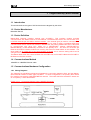
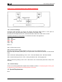
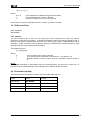
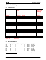
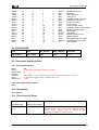
Citect for Windows
Driver Specification Extract
MELSCQNA Driver
Author
Date
Comment
Alain Walgraeve
1998-09-03
Preliminary version
Alain Walgraeve
1998-09-25
Version 1.0
Driver Design Specification
Contents
1.
2.
TARGET DEVICE(S) AND PROTOCOL
4
1.1 Introduction
4
1.2 Device Manufacturer
4
1.3 Device Definition
4
1.4 Communications Method
4
1.5 Communications/Hardware Configuration
4
1.5.1
Wiring Diagrams
4
1.5.2
I/O Device Settings
5
1.5.3
Software Setup
5
1.6 Special Requirements
5
1.7 Maximum Request Length
6
USER INTERFACE
7
2.1 Introduction
7
2.2 Driver Name
7
2.3 Boards Form
7
2.3.1
Board Type
7
2.3.2
Address
7
2.3.3
IO Port
7
2.3.4
Interrupt
7
2.3.5
Special Opt
7
2.4 Ports Form
7
2.4.1
Baud Rate
7
2.4.2
Data Bits
7
2.4.3
Stop Bits
7
2.4.4
Parity
7
2.4.5
Special Opt
7
2.5 IO Devices Form
8
2.5.1
Protocol
8
2.5.2
Address
8
2.6 Pull-down lists Help
8
2.7 IO Device Variable Types
9
2.7.1
Formats and types
9
Citect data types
9
2.7.2
9
MELSCQNA.DBF Entries
MELSCQNA.DOC
26-09-00
2
Driver Design Specification
3.
2.8 PROTDIR.DBF
10
2.9 Parameters and INI options
10
2.9.1
Standard Parameters
10
2.9.2
Driver Specific Parameters
10
2.10
Remapping
10
2.11
Driver Specific Errors
10
2.12
Driver Error Help
11
2.13
Debug Messages
11
2.14
Stats Special Counters
12
2.15
Hints and Tips
12
REFERENCES
13
3.1 References
4.
13
APPENDIX A
14
4.1 AJ71QE71(B5), A1SJ71QE71-B2 and A1SJ71QE71-B5 Hardware.
MELSCQNA.DOC
26-09-00
14
3
Driver Design Specification
1. Target Device(s) and Protocol
1.1 Introduction
This section defines the types of I/O Devices that are targeted by this driver.
1.2 Device Manufacturer
Mitsubishi Electric
1.3 Device Definition
Melsec-QnA Ethernet interface module type AJ71QE71. This interface module provides
communication with Melsec-QnA PLCs via Ethernet. The Melsec-QnA driver can connect with up to
8 TCP/IP channels per AJ71QE71 interface module. One channel (port) is used for communication
with a primary Melsec-QnA PLC; the other ports can then be used for setting up additional Ethernet
communication links to remote I/O modules. Besides that, the primary Melsec-QnA PLC is also able
to communicate with other PLC CPUs via a MELSECNET network (MELSECNET/10,
MELSECNET(ll) or MELSECNET/B) connected to the primary PLC. The limit of 8 channels per
Ethernet AJ71QE71 interface module is a is set by the amount of fixed buffers on this module. The
driver itself has an upper limit of 32 communication channels; this is a driver setting which can be
changed if the need arises.
The Melsec-QnA driver also communicates with AJ71QE71-B5, A1SJ71QE71-B2 and A1SJ71QE71B5 Ethernet interface modules.
1.4 Communications Method
10BASE5 or 10BASE2 Ethernet cable.
1.5 Communications/Hardware Configuration
1.5.1 Wiring Diagrams
The following functional/layout diagrams illustrates the connection between Citect and the MelsecQnA Ethernet interface module type AJ71QE71. In these configurations, the primary QnA Series
PLC itself is connected to a MELSECTNET/10 network. The nodes which are marked as remote can
be occupied by a Citect Workstation.
Figure 3.5.1.1 : Connection Diagram Using 10BASE5 (Ethernet)
MELSCQNA.DOC
26-09-00
4
Driver Design Specification
Figure 3.5.1.2 : Connection Diagram Using 10BASE2 (Cheapernet)
1.5.2 I/O Device Settings
Concerning data exchange, the driver will support both Binary Mode (SW2 on front panel of
AJ71QE71 OFF) and ASCII Mode (SW2 on front panel of AJ71QE71 ON).
Normally SW1 and SW8 will be OFF, while SW3 and SW7 will be ON. SW4-6 are not used.
Important information for using Citect. For Detailed information see Appendix A.
SW1 – OFF
SW2 – OFF(ON)
SW3 – OFF
SW7 – ON
SW8 – OFF
Mode = 0
SW1 is TCP timeout control.
SW2 is Communications type.
Mitsubishi Programming software MMPlus needs this to be set to ASCII Mode (ON).
Citect normally uses Binary Mode (OFF), but a parameter should allow the selection of ASCII Mode
(ON).
SW3 is Self start enabling/disabling of PLC. OFF = Self start Disabled, ON = Self start Enabled.
SW7 is Write Protecting the PLC. OFF = Writing Prohibited, ON = Writing Approved.
SW8 is Initial timing setting of PLC. OFF = Quick start, ON = Normal start (start after a delay of 20
seconds).
1.5.3 Software Setup
The PLC must be programmed to operate the AJ71QE71 interface. A sample program will be given
in Appendix A at a later stage in the testing phase of the driver.
1.6 Special Requirements
None
MELSCQNA.DOC
26-09-00
5
Driver Design Specification
1.7 Maximum Request Length
2048 bits (256 bytes)
MELSCQNA.DOC
26-09-00
6
Driver Design Specification
2. User Interface
2.1 Introduction
This section defines how the user will see the driver. This relates directly to how the Citect forms
need to be filled out and any special INI options. For the kernel, the debug trace messages and the
Stats.Special counters are documented.
2.2 Driver Name
MELSCQNA
2.3 Boards Form
2.3.1 Board Type
TCPIP
2.3.2 Address
0
2.3.3 IO Port
Leave blank
2.3.4 Interrupt
None
2.3.5 Special Opt
Leave blank, not used, was previously used as the ACPU time out in milliseconds in form -time
(default -t2500)
2.4 Ports Form
2.4.1 Baud Rate
This field is not used
2.4.2 Data Bits
This field is not used
2.4.3 Stop Bits
This field is not used
2.4.4 Parity
This field is not used
2.4.5 Special Opt
The AJ71QE71 Ethernet module’s TCP/IP address and port number in the form:
MELSCQNA.DOC
26-09-00
7
Driver Design Specification
-Ia,b,c,d -Pp -T
Where:
a.b.c.d
n
-T
is the destination IP address using decimal numbers,
is the destination port number in decimal,
forces the TCPIP driver to use TCP not UDP.
Previously the format for the address was a.b.c.d:port, eg. 192.9.2.50:1280
2.5 IO Devices Form
2.5.1 Protocol
MELSCQNA
2.5.2 Address
The CPU number (0-64 or 255. You can specify the CPU monitoring time using the optional
parameter /Tt after the CPU number. It should be possible to specify the network number (0-239 or
255) by using optional parameter /Nn after the CPU number (only useful for MELSECNET/10 PLC
networks). Finally we need to have the ability to specify the ASCII Mode for data exchange by using
optional parameter /A (the default is Binary Mode).
The address format is:
a [/Tt] [/Nn] [/A]
Where:
a
t
n
CPU number 0 to 64 or 255 in decimal
CPU monitoring time parameter (units 250 ms.). The default is 10.
Network number 0 to 239 or 255 in decimal. The default network number is
0.
NOTE :
- An in-depth description of the Network and CPU numbering policy can be found in section 10.1 of
the QnA Ethernet Interface Module User’s Manual (see 8. References and Contacts).
2.6 Pull-down lists Help
The following entries should be included in the Citect HELP.DBF spec file.
TYPE
DATA
PROTOCOL
MELSCQNA
MELSCQNA.DOC
FILTER
26-09-00
8
Driver Design Specification
2.7 IO Device Variable Types
2.7.1 Formats and types
IO Device Type
Citect data
format
Citect data types
Input relay
Output relay
Link input
Link output
Internal relay
Link relay
Latch relay
Annunciator
Edge relay
Step relay
Special relay
Special relay for link
Timer (Contact)
Timer (Coil)
Integrat. timer (Contact)
Integrat. timer (Coil)
Counter (Contact)
Counter (Coil)
Timer (Current value)
Integrat. timer (Current value)
Counter (Current value)
Data register
Link register
Special register for link
Special register
File register (block access)
File register (seq. access)
Index register
X<hexno>
Y<hexno>
DX<hexno>
DY<hexno>
M<no>
B<hexno>
L<no>
F<no>
V<no>
S<no>
SM<no>
SB<hexno>
TS<no>
TC<no>
SS<no>
SC<no>
CS<no>
CC<no>
TN<no>
SN<no>
CN<no>
D<no>
W<hexno>
SW<hexno>
SD<no>
R<no>
ZR<hexno>
Z<no>
DIGITAL
DIGITAL
DIGITAL
DIGITAL
DIGITAL
DIGITAL
DIGITAL
DIGITAL
DIGITAL
DIGITAL
DIGITAL
DIGITAL
DIGITAL
DIGITAL
DIGITAL
DIGITAL
DIGITAL
DIGITAL
INT, BCD, LONG, LONGBCD, STRING
INT, BCD, LONG, LONGBCD, STRING
INT, BCD, LONG, LONGBCD, STRING
INT, BCD, LONG, LONGBCD, STRING
INT, BCD, LONG, LONGBCD, STRING
INT, BCD, LONG, LONGBCD, STRING
INT, BCD, LONG, LONGBCD, STRING
INT, BCD, LONG, LONGBCD, STRING
INT, BCD, LONG, LONGBCD, STRING
INT, BCD, LONG, LONGBCD, STRING
Where : <no>
<hexno>
Description/
Special Usage/
Limitations/
1
Valid Ranges
Read/Write
Read/Write
Read/Write
Read/Write
Read/Write
Read/Write
Read/Write
Read/Write
Read/Write
Read/Write
Read/Write
Read/Write
Read/Write
Read/Write
Read/Write
Read/Write
Read/Write
Read/Write
Read/Write
Read/Write
Read/Write
Read/Write
Read/Write
Read/Write
Read/Write
Read/Write
Read/Write
Read/Write
decimal number
hexadecimal number
2.7.2 MELSCQNA.DBF Entries
TEMPLATE
X%X
Y%X
DX%X
DY%X
M%U
B%X
L%U
F%U
V%U
SM%U
1
UNIT_TYPE
0
1
2
3
4
5
6
7
8
9
RAW_TYPE
0
0
0
0
0
0
0
0
0
0
BIT_WIDTH
1
1
1
1
1
1
1
1
1
1
LOW
0
0
0
0
0
0
0
0
0
0
HIGH
0x1FFF
0x1FFF
0x1FFF
0x1FFF
8191
0x1FFF
8191
2047
2047
2047
COMMENT
Input relay
Output relay
Link input
Link output
Internal relay
Link relay
Latch relay
Annunciator
Edge relay
Special relay
See table in 4.7 above for allowed range of addresses in commands.
MELSCQNA.DOC
26-09-00
9
Driver Design Specification
SB%X
S%U
TS%U
TC%U
SS%U
SC%U
CS%U
CC%U
TN%U
SN%U
CN%U
D%U
W%X
SW%X
SD%U
R%U
ZR%X
Z%U
10
11
12
13
14
15
16
17
18
19
20
21
22
23
24
25
26
27
0
0
0
0
0
0
0
0
1
1
1
1
1
1
1
1
1
1
1
1
1
1
1
1
1
1
16
16
16
16
16
16
16
16
16
16
0
0
0
0
0
0
0
0
0
0
0
0
0
0
0
0
0
0
0x7FF
8191
2047
2047
2047
2047
1023
1023
2047
2047
1023
12287
0x1FFF
0x7FF
2047
32767
0xFE7FF
15
Special relay for link
Step relay
Timer (Contact)
Timer (Coil)
Integrating timer (Contact)
Integrating timer (Coil)
Counter (Contact)
Counter (Coil)
Timer (Current value)
Integrating timer (Current value)
Counter (Current value)
Data register
Link register
Special register for link
Special register
File register (block access)
File register (seq. access)
Index register
2.8 PROTDIR.DBF
TAG
FILE
BIT_BLOCK
MAX_LENGTH
OPTIONS
MELSCQNA
MELSCQNA
2048
2048
0x33f
2.9 Parameters and INI options
2.9.1 Standard Parameters
Block
Delay
MaxPending
Polltime
Timeout
Retry
WatchTime
256
0 ( should be increased to lower CPU load )
2
0
2000 msec ( = 2 sec. / Mitsubishi recommends a default value of 10 sec. )
2 ( Mitsubishi recommends a default value of 3 )
30 sec
2.9.2 Driver Specific Parameters
None.
2.10 Remapping
Not supported.
2.11 Driver Specific Errors
Driver Error Code
Mapped to
(Hexadecimal)
(Generic Error label)
Meaning of Error Code
10000h +
code
Code is the Error Code.
Consult section 17.1.3 of the QnA Ethernet Interface
Module User’s Manual (see 8. References and
Contacts) for details on the Error Code.
MELSCQNA.DOC
26-09-00
10
Driver Design Specification
2.12 Driver Error Help
The following entries should be included in the Citect PROTERR.DBF spec file.
PROTOCOL
MASK
ERROR
MESSAGE
REFERENCE
MELSCQNA
0FFFF
10000
*MELSCQNA
Error Code
Section 17.1.3 of
the QnA Ethernet
Interface Module
User’s Manual.
ACTION
COMMENT
2.13 Debug Messages
The driver will incorporate trace functionality to allow support and advanced users to assess
their own syslog traces for the protocol. The trace information will be communicated to Citect
by means of parameters to the channel debug function (as described in Chapter 7. of the DDK
V2.0). The following actions can be traced if the focused communication channel is placed into
the appropriate debug mode.
-
writing data
Driver calls debug() with :
title parameter : “Transmit”
buffer parameter : pointer to the channel request buffer
length parameter : the request length
-
reading data
Driver calls debug() with :
title parameter : “Receive”
buffer parameter : pointer to the channel response buffer
length parameter : the response length
-
communication errors
a. In case of general communication errors :
Driver first calls debug() with :
title parameter : “ERROR: Transmit”
buffer parameter : pointer to the channel request buffer
length parameter : the request length
Then, driver calls debug() with :
title parameter : “Receive”
buffer parameter : pointer to the channel response buffer
length parameter : the response length
b. For timeout errors :
Driver first calls debug() with :
title parameter : “ERROR: Transmit”
buffer parameter : pointer to the channel request buffer
length parameter : the request length
MELSCQNA.DOC
26-09-00
11
Driver Design Specification
Then, driver calls debug() with :
title parameter : “Timeout”
buffer parameter : pointer to the channel response buffer (dummy)
length parameter : the response length (dummy)
2.14 Stats Special Counters
Number
Label
Purpose/Meaning of this counter
0
DCBs to inqueue
Number of messages transmitted.
1
2.15 Hints and Tips
MELSCQNA.DOC
26-09-00
12
Driver Design Specification
3. References
3.1 References
DRIVER DEVELOPMENT KIT V2.0, February 1996, Edition for Citect Windows, Ci Technologies
Pty. Limited.
MELSEC Q series Programmable Controller User’s Manual – QnA Ethernet Interface Module type
AJ71QE71(B5) – A1SJ71QE71-B2 – A1SJ71QE71-B5. Manual number IB (NA) 66661-C
MELSCQNA.DOC
26-09-00
13
Driver Design Specification
4. Appendix A
4.1 AJ71QE71(B5), A1SJ71QE71-B2 and A1SJ71QE71-B5 Hardware.
The B2 has a Coax connector for 10Base2 and the B5 has an AUI connector for 10Base5 type
connections. Mitsubishi recommend using a Transceiver with SQETEST or Heartbeat functionality if
using the B5 model.
Indicators on the front of the Module
RUN
RDY
BSY
SW ERR
COM ERR
CPU R/W
TRAN.S
TRAN.R
FTP
B1 – B8
TEST
TEST.ERR
ON = Normal, OFF = Bad Thing (Normal Operation Display)
Flashing = On-Line and Good (Standard Display of communication
exchange completion)
ON = Executing, OFF= Not Executing (Display during execution of
communication exchange processing)
CPU error, CPU type error, or rotary switch error display
ON = Error, OFF= Normal
ON = Communication Exchange Abnormality (Bad Thing)
ON = Exchanging data with CPU
ON = Data link command request executing
ON = Data link RECV command request waiting
ON = FTP server function operating
Communication line connection status
ON = Open completed, OFF= Closed state
ON = Self diagnosis executing
ON = Error during self diagnosis
Operation Mode Switch
0 = On – Line
1 = Off – Line
2 = Execute a self diagnosis test using a self-loopback test
3 = Execute a RAM Test
4 = Execute a ROM Test
4 = Execute an EEPROM Test
6 – F Not Used
Communication Exchange condition setting Switches
SW1 = TCP Timeout error temporary circuit process selection.
Selection of Circuit processing t the time of a transmission of a TCP time out error.
OFF = Close the circuit
ON = Do Not Close the Circuit
For Citect keep it OFF
SW2 = Data Code Selection
Type of Data Communications
OFF= Binary Mode
ON = ASCII Mode
Mitsubishi has released a Windows version of their programming software that uses ASCII
Mode for communicating with the Module.
Citect normally uses Binary Mode, but there should be an ability to use the ASCII Mode as
well.
SW3 = Self start mode setting
MELSCQNA.DOC
26-09-00
14
Driver Design Specification
Selects the start mode when the QE71 is booted.
OFF= Runs following Y19 (initial processing request signal)
ON = Reads the parameters in the EEPROM buffer memory regardless of the Y19 (initial
processing request signal) after power has been turned on or the module reset and then
conducts initial processing of the contents.
This switch should be OFF.
SW4-SW6 = Usage not possible (Fixed to OFF)
SW7 = CPU communications exchange timing setting
Write Protect the PLC.
OFF = Writing Prohibited
ON = Writing allowed.
If you want to write to the PLC then make sure this is ON
SW8 = Initial Timing Setting
Select the Timing which starts Initial Processing.
OFF= Quick Start (Start without Delay) when entirely constructed in a single network.
OFF = Normal Start (start after a 20 sec delay) when entirely constructed in multiple
networks.
So far OFF has always worked for Citect.
MELSCQNA.DOC
26-09-00
15