1
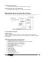
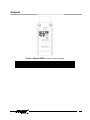
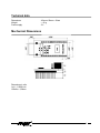
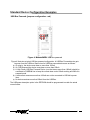
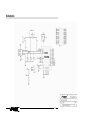
MMusb245RL
User’s
manual
,
lu ard ST Sta rve
a
,
e
o
Ev B VR ers b S l
d
n
io 1, A trol We mo
t
i
a ‘5
in ron ed
r
c
M
e
fo cro dd s
th e rd
s
i
e
b
m m oa rs, pe
C
E
B
e S
I
P its ng roll gh r
K pi
nt Hi fo
r
y
o
rte tot roc FID ers s
o c
r
Pr mi s, R mm lle
a
rs or ler gr
tro
f ol
n
o
B
r
o
c
p
es tr
C
ul on m cro , P or
t c ste mi ms s f
e
d
e
n Sy T
st oar lS
n
y
I
,
s
ro
B
ed PIC or ion ont b
e
s
,
c
R ce luat cro W
V
o
A pr va mi ed iE
ro
dd
ic ng PIC be ds m
M ni T, m
ar rs,
g
E
i
S
o
s
, ts
e
B
de VR Ki ng roll
t
h
i
r
, A rte typ on Hig
1
c
a
‘5 St oto ro ID
r
eic F
s
P
r
m
m
R
le rs or
s, ram rle
r
f
g nt
rv
s
lle
Se ule tro pro oco
s
r s,
od on
m t c tem mic em
i
n ne
t
r Sys ST ys oe
s
,
B
h
et d In PIC sor on i
c
ee R, oce uat mi
p
l
r
V
S A op va IC
er cr
P
E
b
o
,
f
i
g
T
rs s M nin , S
Em g
s
r
R
it
ig
in
le
ol des , AV er K typ
B `51 tart roto roC
S s P mic ,
P for
s
r
r
r
rs
ds olle rwe s fo lle
r
a tr
ro
Se ule ont am
n
o
d c
b
r
c
ro We imo et rog p co
d
in ern
e
o
M
m
dd ds eth ste icr
ar rs, Sy T m r
Bo olle In , S so
tr ed IC oce ign
P
s
co Spe R, opr De
r
V
c
h
B Rtion
ig r A Mi
C
H f o rs
P lua
s, 1 onevasolution
s lle Many ideas
r
e
o tem E rds
m ntr
g
s
a
co
Sy nin Bo
Introduction
Mmusb245RL is a low-cost integrated module designed for data transmission in and out of a
peripheral device or a PC computer via USB interface. It is based on FTDI`s FT245R chip.
MMusb245RL allows data transfer 1MB/s fast. It’s a simple FIFO device and represents an
interface between USB and microcontroller’s parallel interface. There is a USB cable attached to
the module. Windows drivers allow to emulate a serial port on the PC and that provides for
upgrading applications in which transmission over a RS232 serial link was used. Choosing our
Minimodule is the first step for projects, which should be done in a short time. MMusb245 could
be used as a part of a prototype eliminating the necessity of designing a circuit board and in the
final circuit in which the module is fitted “sandwichlike” on top.
MMusb245RL is made in two-layer printed circuit board technology with a solid ground plane.
All signals are accessible via 24 pins, in a 100mils raster (2.54 mm) which allows to use this
module with prototype PCBs. Integral power control makes the MMusb245RL a perfect choice
for USB bus-powered, high power designs as well as self- and low-powered products.
We wish you much success in designing and using new devices !
MMusb245RL Features Summary
•
•
•
•
•
•
•
•
•
•
•
•
•
•
•
•
•
•
•
•
•
Data transmission over USB with speeds up to 1MB/s
256B of FIFO transmit buffer, 128B FIFO receive buffer
integrated 1024bit internal EEPROM
Simple interface to MCU / PLD/ FPGA logic with a 4 wire handshake
FTDI’s drivers provided
Integrated Power-On-Reset circuit with optional in and out reset pins
Integrated AVCC filter
Interface and USB mode configurable in EEPROM memory
Bit-Bang Mode feature (advanced synchronous and asynchronous with two
strobe signals)
Support for bus powered, self powered and high-power bus powered USB configuratoins
Integrated level converter provides interfacing between 5V and 3.3V logic
Integrated FIFO logic level converter
Integrated 3.3V LDO regulator for USB I/O
Power supply from 3.3V to 5.25V
USB bulk data transmit mode
Wake-up capability when in suspend mode
Each device has its own unique ID (FTDIChip-IDTM feature)
UHCI / OHCI / EHCI host controller compatible
USB 1.1 and 2.0 compatible
Standard 0.6in wide 24 pin DIP socket
Standard USB connector, B type
2
Improved features of the FT245R
FT245R converter is a functional equivalent of the FT232R. The only essential difference
between theese devices from a user’s point of view is that the UART of the latter is replaced with
a 8-bit parallel port which interface is similar to a classical FIFO (First In First Out) memory
interface . Just like the FT232R, the FT245R is backward compatible with the previous
generation FT245BM device but far more integrated.
New features:
- integrated EEPROM memory
- integrated USB line resistors
- built in clock signal generator, accessible from the outside byexternal elements
- unique serial number (FTDIChipID)
Possible applications
•
•
•
•
•
•
•
•
USB to RS245 converters
Expanding capabilities of peripheral devices
USB Instrumentation
USB cable and wireless modems
USB Industrial Control
Audio and Video transmission
Toys
Metrology
General Description
MMusb245RL is housed in a single 24-pin module. A single USB port is converted to FIFO
interface, which allows communicating with external devices via a 8-bits bus.
To send data from the peripheral to the host computer, simply write the byte-wide data into the
module when TXE is low. If the transmit buffer fills up or is busy storing the previously written
byte, the device keeps TXE high in order to stop further data from being written until some of the
FIFO data has been transferred over USB to the host.
When the host sends data to the peripheral over USB, the device will switch RXF low to let the
peripheral know that at least one byte of data is available. The peripheral reads data until RXF
goes high which means that there is no more data to read.
The FTDI company provides a Virtual COM Port (VCP) driver with its chip making the peripheral
look like a standard COM port to the PC application software. Most of the existing software
should have no problem cooperating with VCP, you only need to change the ports it uses to the
ones created by the VCP driver. Using VCP the programmer can communicate with the device
the same way as with a regular PC COM port – using Windows VCOMM API or COM port’s
libraries.
The driver incorporates functions defined for the FTDI’s D2XX drivers, which allows the
programmer to integrate the device with the program using Windows DLL.
3
Virtual Com Port (VCP) drivers
• Windows 98/ 98 SE / 2000 / ME / XP, MacOS, Linux 2.4 or newer
D2XX (Direct USB drivers + DLL S/W interface)
• Windows 98 / 98 SE / 2000 / ME / XP / Vista, Linux 2.4 and newer
MMusb245RL Module Simplified Block Diagram
Figure 1. MMusb245RL simplified block diagram
Functional Blocks Description
12MHz Oscillator
The built-in resonator generates a reference clock signal (12MHz) for the x4 clock signal
frequency multiplier. It is used as a clock source for internal modules (SIE, USB Protocol Engine,
FIFO controller).
UART/FIFO general purpose controller includes:
• Integrated Power-On-Reset (POR) Circuit
• Integrated Level Converter on FIFO interface and control signals
• Power Management control for USB devices
• Send Immediate / WakeUp (SI / WU) signal
• Lower Suspend Current
• Programmable FIFO Tx Buffer Timeout
• Bit Bang Mode
• Internal EEPROM
• USB 2.0 full speed
• 3.3V LDO Regulator
• x4 frequency multiplier
• Serial Interface Engine (SIE)
4
•
•
•
FIFO Receive Buffer (128 bytes)
FIFO Transmit Buffer (384 bytes)
FIFO Controller
(more information on www.ftdichip.com)
EEPROM memory
EEPROM allows to customize the USB VID, PID, Serial Number, Product Description Strings
and the Power Descriptor value. EEPROM memory is integrated in the FT245R. It is
programmable using a utility program available on FTDI’s web site www.ftdichip.com and our
homepage www.propox.com.
Module Pin-Out
Figure 2. Mmusb245RL Pin-Out (elements side)
5
Pin Definitions
Pin
mode
Description
1
Pin’s
name
RXF
output
2
TXE
output
3
WR
output
4
RD
input
5
6
7
8
9
10
11
12
15
D7
D6
D5
D4
D3
D2
D1
D0
RST
I/O
I/O
I/O
I/O
I/O
I/O
I/O
I/O
input
16
RSO
output
18
20
3V3
PWRN
output
output
22
23
VIO
VEX
input
input
24
VPO
output
When low, there is data available in the Rx FIFO . High state indicates that
the receive buffer is empty.
Low state indicates that the FIFO is ready to be written to. High state
indicates the transmit buffer being filled or busy writing the last byte.
Writes a data byte from D0..D7 into the transmit FIFO Buffer when WR
changes from high to low.
Enables current FIFO data byte on D0..D7 when low. Fetches the next
FIFO data byte (if available) from the Receive FIFO Buffer when RD
changes from low to high. In high state D0..D7 are in high impedance state.
Data bus line (bit 7)
Data bus line (bit 6)
Data bus line (bit 5)
Data bus line (bit 4)
Data bus line (bit 3)
Data bus line (bit 2)
Data bus line (bit 1)
Data bus line (bit 0)
Can be used by an external device to reset the MMusb245RL. If not
required, tie to VCC
Output of the internal Reset Generator. Stays in high impedance state for
~5ms after VCC exceeds 3.5V and the internal clock start up, then clamps
its output to the 3.3V output of the internal regulator.
Output of the internal LDO regulator.
Goes low when configuration of the device through USB is done. Goes high
when USB is on hold.
Sets voltages on communication pins
Use for applying main power (4.4 to 5.25 Volts) to the module. Connect to
VPO if module is to be powered by the USB port (typical configuration)
Power from USB port.
Additionaly there are pins on the PCB which set the method that the device is powered. Shorted
VEX and VPO pins cause the device to be powered from USB. 3 remaining pins set the voltage
level: 3.3V(VIO-3V3) or 5V(VIO-VEX).
6
Jumpers
Figure 3. Mmusb245RL jumpers view (top layer)
Jumper
JP1
JP2
Description
VEX and VPO pins.
VEX, VIO, 3V3 pins.
7
Technical data
Dimensions
Weight
Power supply
: 45mm x 20mm x 15mm
: ~ 60 g
: 5V
Mechanical Dimensions
Dimensions in mils.
1mil – 1/1000 inch
100mils = 2,54mm
8
Standard Device Configuration Examples
USB Bus Powered (jumpers configuration - red)
Figure 4. Mmusb245RL USB bus powered
Figure 4 illustrates a typical USB bus powered configuration. A USB Bus Powered device gets
its power from the USB bus. Basic rules for USB Bus powered devices are as follows:
a) On plug-in, the device must draw no more than 100mA
b) On USB Suspend the device must draw no more than 500uA.
c) A High Power USB Bus Powered Device (one that draws more than 100mA) should be
connected to PWREN# line to keep the current draw under 100mA working and 500uA in
suspend mode
d) A device that consumes more than 100mA can not be connected to USB hub’s power
lines.
e) No device can draw more that 500mA from the USB Bus.
The USB power descriptor option in the EEPROM should be programmed to match the actual
current intake.
9
Externally powered configuration
Figure 5. Mmusb245RL external power supply
Figure 5 illustrates a typical USB self powered configuration. A USB Self Powered device gets
its power from its own power supply and does not draw current from the USB bus. Basic rules
for USB Self power devices are as follows:
a) A Self-Powered device should not force current down the USB bus when the USB
Host or Hub Controller is powered down.
b) A Self-Powered device can take as much current as it needs during normal operation
and USB suspend as long as it has its own power source.
c) A Self-Powered device can be used with any USB Host and both Bus and Self Powered
USB Hubs.
The USB power descriptor option in the EEPROM should be programmed to a value of zero (self
powered).
10
Bus powered circuit with power control – 5V power supply
Figure 6. Mmusb245RL Bus powered circuit with power control – 5V power supply
In case of configuration as shown on figure 6 the jumpers are not necessary.
Figure 6 illustrates USB bus powered circuit configuration of Musb245RL. External (5V)
devices can be powered from this module.
Basic rules for USB Self power devices are as follows:
a) The external device must have its own power-on-reset circuit to be able to reset when
going back from USB suspend mode
b) The Pull-down option in internal EEeprom should be set to Suspend. Pin PWREN# in
internal EEeprom should be used for switching the supply to external circuits.
c) For devices, which take more than 100mA current from the USB (no device can draw
more that 500mA from the USB Bus) max power parameter in internal EEPROM
should be configured, which informs the system of required power needs.
Technical support
If You have problems with MMusb245RL, please contact us at [email protected].
11
Schematic
12