1
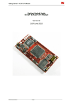
EDP Module Developers Manual – for the RS-EDP System
EDP Module Developers Manual
For the RS-EDP System
Version 1.00
3rd August 2010
Electrocomponents plc
Page 1
EDP Module Developers Manual – for the RS-EDP System
Contents
1.
Introduction
2.
2.1
2.1.1
2.1.2
2.1.3
2.1.4
2.1.5
2.1.6
2.1.7
2.1.8
2.1.9
2.1.10
2.1.11
2.1.12
2.1.13
2.1.14
2.1.15
2.1.16
2.1.17
2.2
2.2.1
2.2.2
2.2.3
2.2.4
2.2.5
2.2.6
2.2.7
2.2.8
Designing a CPU Module
5
Design Considerations .................................................................... 5
Operating Voltage and Vcc_CM selection ...................................... 5
Grounding Arrangement.................................................................. 5
Analogue Voltage Reference .......................................................... 6
RESET Management ...................................................................... 6
Battery Backup Voltage................................................................... 6
Serial UART Communication .......................................................... 7
CAN Communication....................................................................... 7
I2C Interface .................................................................................... 8
SPI Interface ................................................................................... 9
DAC Outputs ................................................................................... 9
Motor Drive Functions ................................................................... 10
Ethernet ......................................................................................... 10
USB Debug ................................................................................... 11
USB Slave ..................................................................................... 11
USB Host ...................................................................................... 11
Mapping the IO Pins to the Signals On the Backplane ................. 11
External Bus .................................................................................. 12
The Design Process ...................................................................... 14
Pin Allocation Spreadsheet ........................................................... 14
Mapping Aid .................................................................................. 16
Schematic Capture ........................................................................ 17
PCB Layout ................................................................................... 17
Getting Started Guide ................................................................... 17
User Manual .................................................................................. 18
Spec Sheet .................................................................................... 18
New Media .................................................................................... 18
3.
3.1
3.1.1
3.1.2
3.1.3
3.1.4
3.1.5
3.1.6
3.1.7
3.1.8
3.1.9
3.1.10
3.1.11
3.1.12
3.1.13
3.1.14
3.1.15
3.1.16
3.1.17
3.2
Designing an Application Module
19
Design Considerations .................................................................. 19
Operating Voltage and Vcc_CM level ........................................... 19
Grounding Arrangement................................................................ 19
Analogue Voltage Reference ........................................................ 20
RESET Management .................................................................... 20
Battery Backup Voltage................................................................. 20
Serial UART Communication ........................................................ 21
CAN Communication..................................................................... 21
I2C Interface .................................................................................. 22
SPI Interface ................................................................................. 23
DAC Outputs ................................................................................. 23
Motor Drive Functions ................................................................... 24
Ethernet ......................................................................................... 24
USB Debug ................................................................................... 25
USB Slave ..................................................................................... 25
USB Host ...................................................................................... 25
Mapping IO Pins From The Backplane to the AM ........................ 25
External Bus .................................................................................. 26
The Design Process ...................................................................... 27
Electrocomponents plc
4
Page 2
EDP Module Developers Manual – for the RS-EDP System
3.2.1
3.2.2
3.2.3
3.2.4
3.2.5
3.2.6
Circuit Schematic .......................................................................... 27
Mapping Aid .................................................................................. 27
Layout............................................................................................ 28
User Manual .................................................................................. 28
Spec Sheet .................................................................................... 28
New Media .................................................................................... 28
4.
4.1
4.2
Software Support
29
CPU Modules ................................................................................ 29
Application Modules ...................................................................... 29
5.
Mechanical Considerations
30
6.
Power Consumption Considerations
31
7.
Further Information
32
Electrocomponents plc
Page 3
EDP Module Developers Manual – for the RS-EDP System
1. Introduction
Before starting to develop a module to fit into the RS-EDP platform it is important to understand the
concept of the RS-EDP system correctly. This information is detailed in the user manuals for the Base
Boards. The manual is called
RS EDP-BB-SystemBaseBoard User Manual Vx Complete.pdf
The Base Boards come in both a 2 position format and a 4 position format, and share a common user
manual. Please read this manual to get an understanding of the system.
Each of the CPU Modules (CM) and Application Modules (AM) has its own user manual, so again
these documents must be read to get an understanding on how to use that particular modules.
The ‘Command Module’ (sometimes referred to as a CPU Module) dictates whether the whole system
is a 3.3V one or a 5.0V one. The user can check the Vcc_CM signal on the break out connector on the
Base Board to determine what voltage the system is when a CM module is fitted. If you are planning to
design a CPU Module then you must manage this pin correctly so the rest of the Application Modules
can reference themselves to it.
To get an appreciation of how the Application Modules are mapped to the backplane and how the
CPU Module can connect to them, a Mapping Aid exists. The one for the LPC1768 module is called...
Mapping Aid RS-EDP - Complete - NXP LPC1768 Rev.XX.pptx
(Name may vary slightly for other modules)
Similarly there are other ones for the other CM modules. This mapping aid is also present in the User
Manual for the CPU Module and at a glance you can see what resources are required to get the best
out of each Application Module.
The other useful documents you will need are the circuit diagram for the modules you want to connect
with each other. These may be contained in the back of the User Manual or available to download
separately off the EDP web site.
So before you start to use the RS-EDP system make sure you have to hand the following documents.
The Circuit Diagram of the modules you intend to use (back of user manual)
The Base Board User Manual
The CPU Module User Manual
The Application Module User Manual
The Pin Allocation Spreadsheet for the CPU Module
The Mapping Aid for the modules
Electrocomponents plc
Page 4
EDP Module Developers Manual – for the RS-EDP System
2. Designing a CPU Module
2.1 Design Considerations
2.1.1
Operating Voltage and Vcc_CM selection
When first starting to develop a CPU Module you must first determine an operating voltage for the
CPU itself. There are currently two voltages supported on the platform, a 5.0V one and a 3.3V one.
The designer of the CPU Module must present out onto the backplane on the Vcc_CM signal a
voltage which is representative of the operating voltage of the CPU. This voltage can be obtained from
the Base Board power supply voltages and routed via a fixed link to the backplane Vcc_CM signal.
You do not need to buffer or current limit this signal. The voltage is used in many places within the
system. Some of them are detailed here.
Vcc_CM
The RESET circuit on the Base Board uses Vcc_CM. The reset signal will pull down to ground via a
transistor when the push button reset switch is pressed and then float up to the Vcc_CM voltage when
the button is released. This means a 3.3V CPU Module will receive a #RESET signal which rises only
to 3.3V and a CPU Module, which is 5.0V, will receive a signal that rises to 5.0V.
In many 5.0V applications the MCU will have an on board A to D converter that uses the 5.0V as a
reference and so the Vcc_CM signal is also used by other modules such as the Analogue Module to
scale the signal accordingly. A 3.3V MCU similarly uses a signal range of 0.0V to 3.3V for it’s A to D
inputs and hence having some indication of this is useful.
The IO on the CPU can similarly be 3.3V or 5.0V, depending upon the processor fitted so the
Application Modules need to be able to level shift also. The Vcc_CM signal is therefore used to help
level shift signals in and out from the Application Modules. The CPU Module does not need to do the
level shifting as the AM modules will do this.
A 5.0V CPU Module will therefore drive the backplane with signals consistent with its IO voltage of
5.0V. Similarly a 3.3V CPU Module will drive the backplane with signals consistent with an IO voltage
of 3.3V.
The I2C interfaces are mapped out on to the Base Board, which is where their pull up resistors reside.
These resistors are nominally fitted to the both the 2 and 4 slot boards and are pulled up to Vcc_CM.
For this reason again you cannot leave the Vcc_CM signal to float and Vcc_CM needs to be hard
wired via a link to either 3.3V or 5.0V.
2.1.2
Grounding Arrangement
Maximum flexibility has been integrated into the grounding arrangements for the CPU Modules.
Analogue singles have their own ground signal, called VAGND, which runs along the backplane
independent from the other grounds within the system. The analogue voltage reference (VAREF), the
analogue signals (AN0-AN15) and the analogue ground (VAGND) are all contained at one end of the
Base Board away from the noisy digital signals. The VAGND does of course need to be connected to
the system ground (SGND) at some point in the system.
VAGND
SGND
12V GND
For this reason the design of the CPU Module must include a user configurable optional link to
connect the VAGND signal and the system ground (SGND) together.
There are three points where the user can connect the two grounds together. These are:
On the CPU Module
On the Base Board
Electrocomponents plc
Page 5
EDP Module Developers Manual – for the RS-EDP System
On the Analogue Module
As the Base Board and Analogue Module have already been designed and provide user link options
for these, then the designer of a new CPU Module must also include a link on the new CPU board.
The 12V Ground (12VGND) and the system ground (SGND) are connected together on the Base
Board near the input power connector. If the designer wishes to use high power (>2A sink) on the
CPU Module he should provide an additional ground terminal via a connector on the CPU Module.
This would allow the user to connect a wire between the 12VGND on the Base Board and the CPU
Module and hence protect the Base Board connectors which are only rated at 2A.
The designer should also provide an optional zero ohm connection between this ground terminal and
the system ground SGND on the CPU Module, to allow the EDP user additional flexibility with respect
to ground referencing.
2.1.3
Analogue Voltage Reference
AN_REF
The CPU may well have an on board A to D converter in which case you might want to provide an
accurate voltage reference for this function. You will need to provide in this case a reference voltage
for the on board analogue which can be either one of the following.
An accurate voltage reference on board the CPU Module itself.
The power supply voltage 3.3V or 5.0V depending on the CPU you are using.
An external voltage reference VAREF provided by the Analogue Module.
All of the CPU Modules designed so far provide the user with link options to select the correct
analogue voltage reference to the CPU Module analogue circuitry.
2.1.4
RESET Management
As mentioned in the operating voltage section the reset voltage is determined by the Vcc_CM output.
Make sure this is set correctly for the MCU module.
The RS-EDP platform in addition to receiving a #RESET signals from the Base Board is also able to
provide a reset out signal called #RESOUT. If your CPU has provision for a reset out function then this
can be mapped on to the #RESOUT signal on the backplane.
#RESIN
#RESOUT
There are no AMs currently in production that use the #RESOUT function, but it has been provided for
future flexibility with modules that have not yet been designed.
Not all CPU’s have a RESOUT function so the majority of the AM modules use the standard RESET
signals should the system need to be reset.
2.1.5
Battery Backup Voltage
If the CPU Module is designed to run a real time clock (RTC) for example, then you might want to
provide an auxiliary voltage to maintain the RTC during power down. The Base Boards have provision
for a battery which can be optionally fitted by the EDP user. This battery voltage is present on the back
plane and is called VBATT.
3V BAT
Quite often, however the user does not want to populate the Base Board with a battery but want to be
able to run the real time clock. With this in mind you will need to provide a link option to select
between the VBATT signal on the backplane and the 3.3V system supply voltage. This would
Electrocomponents plc
Page 6
EDP Module Developers Manual – for the RS-EDP System
effectively allow the user to power the RTC circuit from the main 3.3V supply or VBATT depending
upon the link option selected.
2.1.6
Serial UART Communication
The Base Board has two channels of TTL level UART signals referred to as ASC0_RX/ASC0_TX for
channel 0 and ASC1_RX/ASC1_TX for channel 2. The signals are logic level and will be either 3.3V or
5.0V levels depending upon the CPU fitted.
The Application Modules which use the ASC0 and ASC1 logic level signals are able to deal with both
3.3V and 5.0V signals so the CPU Module designer does not have to level shift these on the CPU
Module .
ASC0_RX_TTL
ASC0_TX_TTL
ASC1_RX_TTL
ASC1_RX_TTL_ASC0_DSR
ASC1_TX_TTL
ASC1_TX_TTL_ASC0_DTR
The Communications Module has facilities to translate the logic level signals into either RS232 levels
or single ended duplex communication or into RS485 signals for differential simplex communication.
ASC0 can be RS232 whilst ASC1 can be either RS485 or RS232.
For RS485 communication a direction pin is needed. In this case ASC1_RX_TTL_ASC0_DSR is used.
The designer must therefore map a general purpose IO pin to this backplane signal so the RS485
communication can be controlled.
It is not possible with the current Communications Module to implement full handshaking on the UART
signals.
2.1.7
CAN Communication
The Base Board has three channels of CAN communication provided, one is for physical layer signals
and the other two are for logic level signals. The Base Board backplane signals for the physical layer
and CANH and CANL and the backplane signals for the logic level ones are CAN0_RX/CAN0_TX and
CAN1_RX/CAN1/TX for channel 0 and 1 respectively.
CAN0_RX
CAN0_TX
CAN1_RX
CAN1_TX
CANH0
CANL0
If the designer has a CAN peripheral on the CPU, the designer should put a physical layer CAN chip
on the module as well. The physical CAN device should then map to the provided signals on the
backplane, signals CANH and CANL.
The designer should also provide a facility, via link options, to allow the connection of the logic levels
signals CAN0_TX/CAN0_RX and/or CAN1_TX/CAN1_RX to the backplane. This way the user can
decide if he wants to use the logic level CAN or the physical layer CAN signals in his application.
The Communications Module for example provides a standard 9 way D connector which effectively
connects the outside world CAN network to the RS-EDP CAN network. This on board D connector,
routes the physical layer CAN, provided by the CPU Module.
The user of the CPU Module would therefore ensure that the links are selected in a way as to use the
on board CAN transceiver on the CPU Modules so that physical layer CAN signals are ported down on
to the backplane and out via the 9 way D connector on the Communications Module.
Electrocomponents plc
Page 7
EDP Module Developers Manual – for the RS-EDP System
The Communications Module also has an isolated CAN network which works on logic level CAN
signals CAN0_RX/CAN0_TX and CAN1_RX/CAN1_TX. The CAN channel either 0 or 1 is selected via
link options on the Communication Module and isolated via a DC:DC converter. The resulting physical
layer CAN from this is then made available on one of the pin headers on the Communications Module.
This isolated CAN is not available on the D connector. See circuit diagram for more info on this.
The user can therefore select an isolated CAN function for his CPU Module by:
Routing the logic level CAN0_RX/TX or CAN1_RX/TX signals from the CPU Module down the
back plane.
Using the Communications Module and selecting via the link options on the Communications
Module the appropriate CAN0/CAN1 signals.
The user can therefore select a NON isolated CAN function for his CPU Module by:
Routing the physical layer CAN signals CANH and CANL from the CPU Module down the
back plane.
Using the Communications Module and the on board D Connector.
The terminating resistors for the CAN network also need to be considered as well. The designer of
the CPU Module must provide a 120ohm terminating resistor for the network. This must be user
selectable either via a link option or a solder bridge.
There are several terminating resistor in the RD-EDP system. These include a 120ohm resistor on the
Base Board for the CANH and CANL signals. There is one terminating resistor per Base Board slot.
The user must remember that these may well be fitted by default and hence selecting a physical layer
CAN device on the CPU Module as well as the terminating resistor may cause problems. This is up to
the user to decide how he wants to arrange his terminating CAN network resistors.
There is also a terminating resistor on the Communication Module for the isolated CAN network only.
No terminating resistor is currently included for the physical layer CAN network.
2.1.8
I2C Interface
There are three I2C interfaces currently implemented on the Base Board. These are CNTRL_I2C,
I2C_GEN0 and I2C_GEN1.
The primary I2C interface on the RS-EDP system is called CNTRL_I2C which comprises of a clock
(CNTRL_I2C_SCL ) and a data line (CNTRL_I2C_SDA). The I2C interface pulls up via pull resistor
present on the Base Board. The designer does not need to provide pull ups on the CPU Module as
they are not required. The pull up voltage is determined by the Vcc_CM signals. (See section on
Vcc_CM selection).
CNTRL_I2C_SCL
CNTRL_I2C_SDA
I2C_GEN0_SCL
I2C_GEN0_SDA
I2C_GEN1_SCL
I2C_GEN1_SDA
This CNTRL_I2C is fundamental to the RS-EDP system as it is used to talk to the Application Modules
and the Base Board. You should design the CPU Module to use the full speed of the I2C bus,
400KHz, as all the modules have been designed to accommodate this bus speed.
The CNTRL_I2C is used for lots of functions including
Base Board for the DIP switch reading and the serial EEPROM access
Digital IO module for input and output
Communication Module for Real Time Clock interface
Analogue Module for on ADC reading and digital potentiometers
Electrocomponents plc
Page 8
EDP Module Developers Manual – for the RS-EDP System
MC2 Motor Drive for controlling brushless DC motors.
The other two I2C interface I2C_GEN0 and I2C_GEN1 do not have any specific purpose in the RSEDP system and are provided for the benefit of the user applications.
It is possible with some of the Application Modules to select between CNTRL_I2C and I2C_GEN0 so
as to allow the inclusion of more than one module to be added and to be controlled via a different I2C
network.
Each of the I2C networks has an interrupt associated with them. These are detailed below.
IRQ_GPIO16_CNTRL_I2C_INT
IRQ_GPIO18_I2C_GEN0_INT
IRQ_GPIO20_I2C_GEN1_INT
IRQ_GPIO22_I2C_INT
The designer should therefore provide an interrupt input pin for each of the I2C networks he intends to
use. A general one called IRQ_GPIO22_I2C_INT is available if there are not enough pins on the
MCU.
The main one to consider is the IRQ_GPIO16_CNTRL_I2C_INT pin which is specifically allocated to
work with the main CNTRL_I2C interface.
2.1.9
SPI Interface
There are two Serial Peripheral Interface (SPI) channels on the RS-EDP platform. The main SPI
interface is called CNTRL_SPI which comprises of four signals below.
CNTRL_SPI_#CS_NSS
CNTRL_SPI_CLK
CNTRL_SPI_MRST
CNTRL_SPI_MTSR
These signals are data in, data out, clock and chip select. The designer can choose to route his SPI
signals down on to the backplane and/or use them locally on the CPU Module. Several of the CPU
Modules designed so far use the SPI for talking to SD cards. The designer can therefore choose to put
a small SD card socket on the CPU Module and use his SPI to talk to the SD card, or via link options
and map down on to the backplane.
None of the EDP Application Modules designed so far use the SPI peripheral other than locally for the
SD card interface. It is however, worth making provision for SPI in some way on your design of the
CPU Module as it is likely there will be a module that will want to use it at some point.
The other SPI peripheral bus that is made available in the backplane mapping is the SPI_SSC.
SPI_SSC_#CS_NSS
SPI_SSC_CLK
SPI_SSC_MRST_MISO
SPI_SSC_MTSR_MOSI
This is made available as a general purpose SPI bus for the user own application.
2.1.10 DAC Outputs
If the designer has a CPU with dedicated DAC output then he can map them to the pins detailed
below.
Electrocomponents plc
Page 9
EDP Module Developers Manual – for the RS-EDP System
CPU_DAC01_GPIO19
CPU_DACO0_GPIO17
Alternatively a PWM output pin on the MCU should be mapped here. The CPU_DACx backplanes
functions are used to drive some of the motor drive functions on the MC1 Motor Drive Application
Module.
2.1.11 Motor Drive Functions
If the MCU has on board motor drive functions then the designer can choose to map these to the
backplane on the following pins.
EMG_TRAP
MOTOR_TCO_FB
MOTORH0_ENC0
MOTORH1_ENC1
MOTORH2_ENC2
MOTORP0H
MOTORP0L
MOTORP1H
MOTORP1L
MOTORP2H
MOTORP2L
MOTORPWM
The EMG_TRAP pin is reserved for an emergency stop input pin. This could come from a threshold
current detector in a motor drive motor or an emergency stop button for example. The designer should
therefore make sure the MCU pin has a flexible interrupt on it.
The MOTOR_TCO_FB pin is for motor tacho feedback and so the designer should map this to an
MCU function that provides an input capture type function. Pulses streams from the MC1 Motor Drive
Module give indication of rotational speed in the motor drive application. This pin should therefore
have an input compare type functionality..
The MOTORH0_ENCx pins are used for rotary encoder type functions. If the MCU being designed
has a rotary encoder input capability then map these pins to these backplane signals. Alternatively if
you are using Hall Effect sensors for three phase motor driving you should use these signals also.
For driving three phase bridges make sure the MCU if it has this function is mapped to the motor
phase signals MOTORPxH and MOTORPxL. A total of 6 signals are used in a classic bridge
arrangement for driving of such motors. The MC2 motor drive module has the provision to take these
signals from an external MCU and to drive a single 100W motor, 24V @ 4A.
The MOTORPWM signal is for a standard DC motor that requires a single simple PWM signal to drive
it. The MC1 motor drive module makes use of this signal.
2.1.12 Ethernet
If the MCU has an Ethernet MAC on board then you will need to map it to the Ethernet PHY and
connector on the Base Board. The Ethernet signals are the standard ones as detailed below.
Map your MCU to these signals if you want to use the Ethernet PHY and connector on the Base
Board. The PHY can be used with standard 10/100 Ethernet traffic.
ETH_LNK_LED
ETH_RXETH_RX_LED
ETH_RX+
Electrocomponents plc
Page 10
EDP Module Developers Manual – for the RS-EDP System
ETH_SPD_LED
ETH_TXETH_TX+
2.1.13 USB Debug
The Base Board has been provided with two USB debug signals, USB_DEBUG_D- and
USB_DEBUG_D+.
USB_DEBUG_DUSB_DEBUG_D+
These two signals allow the user to plug a debug tool into the Base Board and for these two signals to
be routed through the backplane into the CPU Module. The STR9 and the XC167 module use an FTDI
debug interface chip to facilitate the debugging of the MCU code. The PC based Integrated
Development Environment (IDE) tool used is HiTOP from Hitex. A version of HiTOP is made available
for the debugging of STR9 and XC167 devices.
The designer can also use these USB debug signals for his own purposes of debugging, but they
should not be used for general USB communication with the host PC as there are additional USB
supported lines available. See below.
2.1.14 USB Slave
If the MCU supports USB slave then there are two lines on the backplane to which the USB signals
should be mapped. These are detailed below.
USB_DEV_DUSB_DEV_D+
These are standard USB signals which are routed via the Communication Board which has on board a
mini USB connection and input protection circuit on it. The designer if he so wishes can included a
mini USB connection on his CPU Module.
2.1.15 USB Host
As USB host is a bit different from USB slave, a separate set of connections has been made available.
These are on the backplane and detailed as shown below.
USB_HOST_DUSB_HOST_D+
The USB host connections are not currently used anywhere in the system so there is little point at
present mapping the MCU pins to these signals. It would probably be better to allow a link option to
the USB slave connections and at least you have access to them via the mini USB connector on the
Communications Module.
Another more elegant solution would be to put a min USB connection on the CPU Module and not rely
on the user having a Communications Module.
2.1.16 Mapping the IO Pins to the Signals On the Backplane
This is by far the hardest task as the majority of the resources may well have been used already with
the mapping of the peripherals to the backplane. You will need to study each of the currently available
Application Modules and identify which signals are used to control the function on them.
You will then need to map down the MCU pins onto these backplane signals. To help with this it is
better to create a pin allocation spreadsheet which details the resources you have already used and
Electrocomponents plc
Page 11
EDP Module Developers Manual – for the RS-EDP System
the ones you have left. You can systematically go through each of the backplane functions and assign
them to an MCU pin. This has been done for each of the currently existing CPU Modules and the Pin
Allocation Spreadsheets made available to the users.
You may well want to use one pin for two different backplane functions thereby allowing the user more
flexibility in the configuration of the system. It is better to use a link option or solder bridge to select the
required function rather than hard wiring two backplane functions together.
Once you have allocated all of the pins you can produce a Mapping Aid document which will describe
the backplane resources used. This is useful for determining if all of the functions of a AM can be used
or not. There is usually some compromise in each system and not all of the function on a AM can be
used by a CPU CM.
To help with the mapping, the naming convention of the backplane functions gives some idea as to
what they are used for.
The EVG prefix stands for event generation and hence any PWM type pins or general purpose output
pins should be mapped to these backplane functions.
The EVM stands for event measurement and hence should be used for pins with input capture or
general purpose inputs.
The GPIO pins as their name suggests are general purpose inputs.
There are some other dedicated function pins such as smart card interface (MCI) and I2S for digital
audio but these are not currently used anywhere in the system.
If the MCU has a dedicated smart card interface then I suggest mapping the MCU pins to an on board
SD card interface rather than using the standard SPI peripheral to do this. This will prove a lot faster
access to the card and will make better use of the facilities of the MCU. In this case there would be no
need to map to the backplane signals as this would require an SD card interface on another module
for it to have any value.
2.1.17 External Bus
If the MCU you are using has an external bus and you want to make this available on the back plane
then it is possible to do this by using the appropriate bus signals. These signals are detailed below.
#CS0
#CS1
#CS2
#CS3
#PSEN
#RD
#WR
#WRH
A0_AD0
A1_AD1
A2_AD2
A3_AD3
A4_AD4
A5_AD5
A6_AD6
A7_AD7
A8_AD8
A9_AD9
A10_AD10
A11_AD11
Electrocomponents plc
Page 12
EDP Module Developers Manual – for the RS-EDP System
A12_AD12
A13_AD13
A14_AD14
A15_AD15
ALE
The external bus backplane signals are relatively straight forward to interpret. You can see the bus is
multiplexed 16bit bus AD0-AD15 with an ALE function to latch the address. The read and write signals
are provided by #RD and #WR and the chip select signals are provided by CS0-CS3.
There are not currently any AM’s that use the external bus. The STR9 module is currently mapped out
to use the external bus if required. It is currently implemented with an external 1M byte SRAM device.
Refer to the Base Board user manual for more information on the pin signals and the STR9 manual for
an example as how to lay out the CPU Module for external bus addressing over the backplane.
Electrocomponents plc
Page 13
EDP Module Developers Manual – for the RS-EDP System
2.2 The Design Process
2.2.1
Pin Allocation Spreadsheet
Have a look at the existing ones and copy the method used in them. Create a new spreadsheet for
yourself.
In the first tab of the spread sheet (called Pin Allocation), type in all the names of the pin functions
from the user manual of the MCU datasheet. Reference each name with each pin number.
STR912
Pin
1
2
3
4
STR912 Pin
Name
P4.2
P4.1
P4.0
AVSS Analog
GND
STR912
Function
Analogue
Analogue
Analogue
Analogue
Ground
Comment
When you finish this you will have a complete list of all the MCU pins and names.
You will now need to allocate these to the backplane signals on the Base Board.
The Base Board signals you will find in one of the existing Pin Allocation Spreadsheets. It is usually
the last tab in the spreadsheet.
RS-EDP-BASE
BOARD
Name
AN_REF
AN0
AN1
AN2
AN3
AN4
AN5
EDPCON1
1
3
4
5
6
7
8
EDPCON2
Comment
Base Board require a Vref signal
Copy and paste this spread sheet so it lies to the right hand side of the pin allocation in an area that is
a few columns further right than the pinning information you already have.
Starting with the easiest of the signals to map such as the Ethernet and the USB copy across the
information contained in the backplane section in to the Pin Allocation section.
STR912
Pin
1
2
3
4
5
6
STR912 Pin
Name
P4.2
P4.1
P4.0
AVSS
Analog
GND
P7.0
P7.1
STR912
Function
Analogue
Analogue
Analogue
Analogue
Ground
Comment
GPIO
GPIO
RS-EDP Mapping
AN2
AN1
AN0
EDPCON
1
5
4
3
VAGND
MOTORH0_ENC0
MOTORH1_ENC1
19
116
118
EDPCON
2
Each time you do this mark in the backplane diagram with small X in a column to indicate that you
have already used that backplane resource.
RS-EDP-BASE
Electrocomponents plc
Page 14
Comment
rotary encoder
rotary encoder
EDP Module Developers Manual – for the RS-EDP System
X
X
X
BOARD
Name
AN_REF
AN0
AN1
AN2
AN3
EDPCON1
1
3
4
5
6
EDPCON2
Comment
Base Board require a Vref signal
Each time you allocate more of the backplane resource to the MCU pinning you will find you have less
to allocate. Eventually you will be left with just the IO pins of the MCU and the GPIO,EVG, & EVM pins
to allocate.
Once you have had a first pass at allocating the resource, you may well want to add several back
plane signals to one I/O pin. For example a UART peripheral may share the same pin as the high
speed PWM output pin. In this case you might want to add a link option to your design to allow the
user to select between UART and PWM. In this case you need to insert a line into the spread sheet
and add the new link option.
STR
912
STR912
Pin
STR912
Pin
Name
Function
1
P4.2
Analogue
2
3
4
P4.1
P4.0
AVSS
Analog
GND
Comment
RS-EDP Mapping
Analogue
Analogue
EDPC
ON
EDPC
ON
1
2
Comment
3 options
AN2
5
3 options
EVG3_GPIO46
67
3 options
EVG11_GPIO59
80
2 options
AN1
4
2 options
EVG1_GPIO42
63
4 options
AN0
3
4 options
EVG0_GPIO40
61
Output with PWM capability
4 options
EVG2_GPIO44
65
Output with PWM capability
4 options
EVG9_GPIO57
78
VAGND
19
Output with PWM capability
Output with PWM capability
Analogue
Ground
You can see that P4.2 of the STR912 device has three back plane options, AN2, EVG3_GPIO46 and
EVG11_GPIO59. The ‘comment’ field has been entered with the number of options that pin has.
At the end of the mapping exercise you can copy and paste the items in the ‘RS-EDP Mapping’
column into a new area of the spread sheet. You can then sort just these items into alphabetical order
and you will get a complete list of all the resources on the back plane you have used. This should
include the RESET signals, the analogue and system ground as well as the peripherals etc. You will
need this list later on to include in the User Manual for your board and to help in preparation with the
Mapping Aid.
You can also copy and paste a list of the MCU pin names along with the pin number. This allows for
easier finding of pin signals in the circuit when you see them. This is a great help when debugging and
fault finding. You can include this in the User Manual as well.
After completing this exercise you should have a spread sheet with multiple tabs with the following
information available.
A ‘pin allocation tab’ containing
A list of MCU pin number and the MCU pin name along with the RS-EDP back plane names to
which it is mapped. You should also have the EDPCON1 and EDPCON2 pin numbers.
A colour coded list of the back plane resources used, sorted by colour and then alphabetical.
This allows you to see at a glance what the MCU module can communicate with over the back
plane.
Electrocomponents plc
Page 15
EDP Module Developers Manual – for the RS-EDP System
The original table of EDP Back Plan signals versus EDPCON1 and EDPCON2 pin numbers.
A ‘pin allocation summary’ tab containing
A list of MCU pin number and the MCU pin name along with the RS-EDP back plane names to
which it is mapped. You should also have the EDPCON1 and EDPCON2 pin numbers.
A colour coded list of the back plane resources used, sorted by colour and then alphabetical.
This allows you to see at a glance what the MCU module can communicate with over the back
plane.
An alphabetical pin name listing versus MCU pin number.
A ‘Base Board signal name’ tab containing
An alphabetical listing of the Base Board signal names with the EDPCON1 and EDPCON2 pin
numbers plus the breakout connector names and pin numbers.
The breakout connectors are on the Base Board and quickly allows for the probing of signals being
used on the backplane. Pretty much all of the signals are available to monitor via the break out
connectors. This is one of the most useful parts of the document as it quickly allows you to identify
where to probe on the Base Board to monitor a signal. Eg EVG3_GPIO46 can be quickly cross
referenced to P602 pin 19.
EVG3_GPIO46
EVG4_GPIO48
EVG5_GPIO50
EVG6_GPIO52
2.2.2
67
69
71
73
P602
P602
P602
P602
19
20
21
22
Mapping Aid
The mapping aid document needs now to be created. It allows you to see at a glance what MCU
resources are deployed from the CPU Module and how it can interface to the other modules in the
system.
The mapping aids are produced in Microsoft Power Point. When creating the Mapping Aid for a new
processor, start with the Mapping Aid for the Application Modules. All of the AMs are currently
contained in one document called
Mapping Aid AM - RS-EDP Rev.xx.pptx
To start however it is probably better to open an existing one for a CPU Module.
Open this document and you will see each AM has its own page detailing how it interfaced to the back
plane. At the end of the document you can create your own Mapping Aid from the Pin Allocation
Spreadsheet. You can copy the blocks from XL into Power Point and then resize and move them
around to suite.
The Mapping Aid will allow you to quickly identify which AMs the new CPU Module can communicate
with effectively. Where you have an overlap of resource (same name in two boxes) you will have a
good chance of communicating effectively.
Electrocomponents plc
Page 16
EDP Module Developers Manual – for the RS-EDP System
DIO54 - Digital I/O Module Inputs to RS-EDP Backplane
X205 Digital
Input Connector
EVM0_GPIO21
J400
1
EVM1_GPIO23
EVM2_GPIO41_CAPADC
EVM3_GPIO43
EVM4_GPIO45
EVM5_GPIO47
EVM6_GPIO49
EVM7_GPIO51
EVM8_GPIO53
EVM9_GPIO55
EVM10_GPIO68_ASCO_CTS
J400
4
IRQ_GPIO22_I2C_INT
1
IRQ_GPIO16_CNTRL_I2C_INT
IRQ_GPIO18_I2C_GEN0_INT
CNTRL I2C
1
3
B308
2
1
I2C GEN0
7
J400
10
J400
13
J400
16
J401
1
J401
4
J401
7
J401
10
J401
13
J401
16
6
9
12
15
18
3
6
2
5
8
11
14
17
2
5
8
9
12
15
18
11
14
17
2
I2C Data
I2C CLK
DI(0)
DI(1)
DI(2)
DI(3)
DI(4)
DI(5)
DI(6)
DI(7)
DI(8)
DI(9)
DI(10)
DI(11)
DI(12)
DI(13)
DI(14)
DI(15)
B301
3
2
3
J400
3
I2C
B309
DI(0) – DI(11) can be read via I2C or via backplane by the MCU
DI(12) – DI(15) can only be read via I2C.
Use your imagination to create a mapping aid similar to the ones you see here.
2.2.3
Schematic Capture
Once the Pin Allocation Spreadsheet and the Mapping Aid are produced and you are happy with the
outcome, you can proceed to design the circuit schematic for the new CPU Module. Jumper links are
preferred to solder bridges and zero ohm resistors, but if space constraints are too tight then solder
bridges can be tolerated. Link options obviously provide the user with an easier way to reconfigure it,
without the need to use a soldering iron.
2.2.4
PCB Layout
Following schematic capture, the module PCB should be laid out. The mechanical drawings for the
main connectors are at the end of this document. By purchasing an RS-EDP system and a few
modules you will get some idea of the mechanical clearances and how the unit fits together. See
section below on ‘Mechanical Considerations’.
2.2.5
Getting Started Guide
A getting started guide needs to be provided for each new CPU Module that is designed. This should
take the user step by step from knowing nothing about the product to actually plugging it into a Base
Board and getting it to do something. The board should come with software examples that the user
can download, and provide information of how to get up and running with the possible different tool
chains and debuggers required to program and debug code for it. Look at the existing Getting Started
Guides for an example of one.
Electrocomponents plc
Page 17
EDP Module Developers Manual – for the RS-EDP System
2.2.6
User Manual
This is the main reference document that contains the detailed operational information required to use
the new CPU Module. It should contain the circuit diagram and the components overlay drawings as
well as information from the ‘Pin Allocation Spreadsheet’ and some info from the Mapping Aid. It
should be the most comprehensive of the documents and contain all the relevant info to use the
module in a real world application.
2.2.7
Spec Sheet
The CPU Module designer is also expected to provide a one page Spec Sheet with a bulleted list of all
the key features. This should ideally include a picture of the module. It is designed as a quick
reference guide so customer can quickly see what it has and can then go onto download the user
manual if it is of interest. The browsing process is to first find the module description on the web site,
then to click on a link for the spec sheet, and then on to the user manual for more detailed information.
2.2.8
New Media
With the explosive growth in new media the user should make best use of the resource to promote his
design. This includes ‘You Tube’ clips, animated presentations, application notes and training material
to help the user develop skills with the design.
RS now have ‘Design Spark’ which provides the user with a vehicle for blogging and general
promotion/support of new items.
Electrocomponents plc
Page 18
EDP Module Developers Manual – for the RS-EDP System
3. Designing an Application Module
3.1 Design Considerations
3.1.1
Operating Voltage and Vcc_CM level
When first starting to develop a Application Module the designer must first consider the fact that the
CPU Module may be a 5.0V or a 3.3V operating voltage device. This means the designer may well be
faced with signals for #RESET and I2C levels that may be 3.3V or 5.0V. To determine what the
operating voltage is, the designer can use the Vcc_CM signals, which is a zero ohm impedance output
signals that is configured by the fitted CPU Module. This signal is present on the backplane and
designer can use it to help with level shifting.
The CPU Module basically links either the 3.3V or the 5.0V power supply voltages to the backplane
Vcc_CM signal, and hence the designer can draw current from this in accordance with the maximum
current ratings for the 3.3V and 5.0V baseboard signals.
Vcc_CM
The I2C levels have pull up resistors on the Base Board that pull up to Vcc_CM so these levels are
also controlled externally.
The reset circuit on the Base Board uses Vcc_CM. The reset signal will pull down to ground via a
transistor when the push button reset switch is pressed and then float up to the Vcc_CM voltage when
the button is released. This means a 3.3V CPU Module will receive a #RESET signal which rises only
to 3.3V and a CPU Module which is 5.0V will receive a signal that rises to 5.0V. If the AM uses the
#RESET signal then it has to accommodate both 3.3V and 5.0V levels.
The IO on the CPU Module can similarly be 3.3V or 5.0, depending upon the processor fitted so the
Application Modules needs to be able to level shift the data in a way as not to damage the CPU
Module also. The Vcc_CM signal is therefore used to help level shift signals in and out from the
Application Modules. The CPU Module does not need to do the level shifting as the AM modules will
do this.
3.1.2
Grounding Arrangement
The designer of the AM has available to him three types of ground signal. These are shown below.
VAGND
SGND
12V GND
Analogue singles have their own ground signal, called VAGND, which runs along the backplane
independent from the other grounds within the system. The analogue voltage reference (VAREF), the
analogue signals (AN0-AN15) and the analogue ground (VAGND) are all contained at one end of the
Base Board away from the noisy digital signals. The VAGND does of course need to be connected to
the system ground (SGND) at some point in the system.
The VAGND signals are used for referencing precision analogue signals. If the designer wants to use
it he must provide on his AM a user configurable link to connect it to the main system ground SGND.
There are three points where the RS-EDP user can connect the two grounds together. These are:
On the CPU Module.
On the Base Board.
On the Analogue Module.
Electrocomponents plc
Page 19
EDP Module Developers Manual – for the RS-EDP System
As the Base Board and CPU Module have already been designed and provide user link options for
these, then the designer of a new AM must also include a link on this board.
The 12V ground (12VGND) and the system ground (SGND) are connected together on the Base
Board near the input power connector. If the designer wishes to use high power (>2A sink) on the
CPU Module he should provide an additional ground terminal via a high current connector on the CPU
Module. This would allow the user to connect a wire between the 12VGND on the Base Board and the
CPU Module and hence protect the Base Board connectors, which are only rated at 2A.
The designer should also provide an optional zero ohm connection between this 12V GND terminal
and the system ground SGND on the AM to allow the user additional flexibility with respect to ground
referencing.
3.1.3
Analogue Voltage Reference
AN_REF
On the backplane is an Analogue Voltage Reference signal called AN_REF. This voltage reference is
usually supplied by the Analogue Module but in some instances may also be provided by the CPU
Module. The designer of the new AM module cannot assume that this signal is present and therefore if
the user wishes to use a voltage reference signal on his board he must provide one or some of the
three options detailed below.
Provide a link option to AN_REF on the backplane.
Provide a link option to 3.3V or 5.0V system voltage.
Provide his own on-board voltage reference.
3.1.4
RESET Management
As mentioned in the operating voltage section the #RESET voltage is determined by the Vcc_CM
output. Make sure your circuit is able to cope with 5.0V and 3.3V reset levels.
The AM in addition to receiving a #RESET signals from the Base Board is also able to receive a reset
out signal called #RESOUT. This signal is provided by some of the CPU Module. Not all of the CPU
Modules have provision for a reset out function, so use this one with caution. You could provide the
user with the option to select between the #RESET and #RESOUT signals.
#RESIN
#RESOUT
Not all CPU’s have a #RESOUT function so the majority of the AM modules that require a reset use
the standard #RESET signal.
3.1.5
Battery Backup Voltage
The Base Boards have provision for a battery which can be optionally fitted by the designer. This
battery voltage is present on the back plane and its signal is called 3VBATT.
3V BAT
Quite often, however the user does not want to populate the Base Board with a battery but want to be
able to run the real time clock (RTC) for example with the on board supply voltage. With this in mind
you will need to provide a link option to select between the 3VBAT signal on the backplane and the
3.3V/5.0V system supply voltage. This would effectively allow the user to power the backed up circuit
from the main 3.3V supply or 3VBAT depending upon the link option selected.
Electrocomponents plc
Page 20
EDP Module Developers Manual – for the RS-EDP System
3.1.6
Serial UART Communication
The Base Board has two channels of TTL level UART signals referred to as ASC0_RX/ASC0_TX for
channel 0 and ASC1_RX/ASC1_TX for channel 2. The signals are logic level and will be either 3.3V or
5.0V levels depending upon the CPU fitted.
The ‘Application Modules’ which use the ASC0 and ASC1 logic level signals need to be able to deal
with both 3.3V and 5.0V signals. The AM module designer has to level shift these on the CPU Module,
or use device which can cope with both levels (2.5V to 5.5V operation device for example).
ASC0_RX_TTL
ASC0_TX_TTL
ASC1_RX_TTL
ASC1_RX_TTL_ASC0_DSR
ASC1_TX_TTL
ASC1_TX_TTL_ASC0_DTR
The ‘Communications Module’ for example has facilities to translate the logic level signals into either
RS232 levels for single ended duplex communication or into RS485 signals for differential simplex
communication. ASC0 can be RS232 whilst ASC1 can be either RS485 or RS232. The designer can
check the Communications Module schematic to see how this is achieved on this particular module.
For RS485 communication a direction pin is needed. The user can use pretty much use any IO pin
from the MCU to achieve this. The designer of the AM module should therefore choose a backplane
signal to help with this. This backplane signal must of course be available to the CPU Module. You
can determine this by looking at the Mapping Aid for that particular CPU Module.
The designer must therefore map a general purpose IO pin to this backplane signal so the RS485
communication can be controlled.
Full handshaking is theoretically possible as the backplane signals have been made available for this.
In practice, however, the CPU Modules have not been mapped out to accommodate this. The
designer can implement his own handshaking arrangement for a particular CPU Module.
3.1.7
CAN Communication
The Base Board has three channels of CAN communication provided, one is for physical layer signals
and the other two are for logic level signals. The Base Board backplane signals for the physical layer
are CANH and CANL and the backplane signals for the logic level ones are CAN0_RX/CAN0_TX and
CAN1_RX/CAN1/TX for channel 0 and 1 respectively.
CAN0_RX
CAN0_TX
CAN1_RX
CAN1_TX
CANH0
CANL0
If the designer has a CAN peripheral on the AM, then designer should decide whether to use the
physical layer interface or the TTL level interface. The physical CAN device should then map to the
provided signals on the backplane, signals CANH and CANL, whilst the TTL level interface would
need to consider level shifting the 3.3V/5.0V signals from the CPU Module.
The Communications Module if fitted provides a standard 9 way D connector, which effectively
connects the outside world CAN network to the RS-EDP CAN network. This on board D connector,
routes the physical layer CAN, CANH & CANL to the outside word.
Most of the CPU Modules with CAN interfaces on board also have a physical layer device on that
module. The system user therefore decides how to configure the system and whether to use physical
Electrocomponents plc
Page 21
EDP Module Developers Manual – for the RS-EDP System
level or TTL level signals. Consequently the designer of the AM has to accommodate the user’s
decision.
The terminating resistor for the CAN network also need to be considered as well. The designer of the
AM must provide a user selectable 120ohm terminating resistor for the network. This must be user
selectable either via a link option or a solder bridge.
There are several terminating resistors in the RD-EDP system. These include a 120ohm resistor on
the Base Board for the CANH and CANL signals. There is one for each slot on the Base Board. The
user must remember that these may well be fitted by default and hence selecting a physical layer CAN
device on the CPU Module as well as the terminating resistor may cause problems. This is up to the
user to decide how he wants to arrange his terminating CAN resistors.
There is also a terminating resistor on the Communication Module for the isolated CAN network only.
No terminating resistor is currently included for the physical layer non isolated CAN network.
3.1.8
I2C Interface
There are three I2C interfaces currently implemented on the Base Board. These are CNTRL_I2C,
I2C_GEN0 and I2C_GEN1.
The primary I2C interface on the RS-EDP system is called CNTRL_I2C which comprises of a clock
(CNTRL_I2C_SCL ) and a data line (CNTRL_I2C_SDA). The I2C interface pulls up via pull resistor
present on the Base Board. The designer does not need to provide pull ups on the CPU Module as
they are not required. The pull up voltage is determined by the Vcc_CM signals. (See section on
Vcc_CM selection).
CNTRL_I2C_SCL
CNTRL_I2C_SDA
I2C_GEN0_SCL
I2C_GEN0_SDA
I2C_GEN1_SCL
I2C_GEN1_SDA
This CNTRL_I2C is fundamental to the RS-EDP system as it is used to talk to the Application Modules
and the Base Board. You should design the AM to use the full speed of I2C, 400KHz, as all the
modules have been designed to accommodate this bus speed.
The CNTRL_I2C is used for lots of functions including
Base Board DIP switch reading and the serial EEPROM access.
Digital IO Module for input and output.
Communication Module for Real Time Clock interface.
Analogue Module for on ADC reading and digital potentiometers
MC2 Motor Drive for controlling brushless DC motors.
When designing a new Application Module, the user should be aware of the existing I2C address used
by the other AM devices. It is wise to ensure that the new AM can be controlled via the CNTRL_I2C
signals without contention with other I2C device. The Base Board manual describes the I2C address’s
currently in use with the more common AMs.
It is possible with some of the Application Modules to select between CNTRL_I2C and I2C_GEN0 so
as to allow the inclusion of more than one module to be added and to be controlled via a different I2C
network. This is easy to do with a few link options and give additional flexibility to the RS-EDP user so
he can use two I2C buses in his design.
The user should also provide some way of altering the I2C address’s as two identical AMs may be
plugged in to the backplane. In this case the AMs will need slightly different I2C address’s for the
Electrocomponents plc
Page 22
EDP Module Developers Manual – for the RS-EDP System
device as they will be using the same I2C bus. This you can normally do by proving a few link options
to configure the I2C address on the silicon devices.
The other two I2C interface I2C_GEN0 and I2C_GEN1 do not have any specific purpose in the RSEDP system and are provided for the benefit of the user applications.
Each of the I2C networks has an interrupt associated with them. These are detailed below.
IRQ_GPIO16_CNTRL_I2C_INT
IRQ_GPIO18_I2C_GEN0_INT
IRQ_GPIO20_I2C_GEN1_INT
IRQ_GPIO22_I2C_INT
The designer should therefore provide an interrupt input pin for each of the I2C networks he intends to
use. A general one called IRQ_GPIO22_I2C_INT is available if there are not enough pins on the
MCU.
The main one to consider is the IRQ_GPIO16_CNTRL_I2C_INT pin which is specifically allocated to
work with the main CNTRL_I2C interface. You may find these signals also in use by other AMs, such
as the real time clock (RTC) on the Communications Module.
3.1.9
SPI Interface
There are two Serial Peripheral Interface (SPI) channels on the RS-EDP platform. The main SPI
interface is called CNTRL_SPI which comprises of four signals below.
CNTRL_SPI_#CS_NSS
CNTRL_SPI_CLK
CNTRL_SPI_MRST
CNTRL_SPI_MTSR
These signals are data in, data out, clock and chip select.
None of the EDP Application Modules designed so far use the SPI peripheral.
If your application elects to use the SPI interface then make sure it is level shifted to accommodate the
3.3V and 5.0V CPU Modules. Also the SPI_SSC_#CS_NSS chip select signal may well be in use by
another AM, so it is worth making provision for another chip select signal. I would recommend that at
least three other general purpose IO pins be made available for this purpose with link options on the
circuit board allowing the user to configure the system accordingly.
This is particularly useful if three identical AMs are plugged in to one Base Board. If this is the case
then it is likely that each SPI interface will require its own chip select.
The other SPI peripheral bus that is made available in the backplane mapping is the SPI_SSC.
SPI_SSC_#CS_NSS
SPI_SSC_CLK
SPI_SSC_MRST_MISO
SPI_SSC_MTSR_MOSI
This is made available as a general purpose SPI bus for the user own application.
3.1.10 DAC Outputs
The RS-EDP system provides two DAC signals on the backplane. These DAC signals could well be
analogue levels or they could be (more likely) PWM signals. The designer of an AM could therefore
use these to control functions such as motor control speed to audio volume on a module. It is worth
noting that these signals may well be used by other AMs so check the Mapping Aids to see what other
AMs are using. If you require a PWM signal in your AM design then it is worth having a link option to
Electrocomponents plc
Page 23
EDP Module Developers Manual – for the RS-EDP System
these signals as well as link option to other EVGxx signals on the backplane. Having additional ink
options provides an opportunity to resolve contention with other modules.
CPU_DAC01_GPIO19
CPU_DACO0_GPIO17
3.1.11 Motor Drive Functions
If the AM requires some motor drive function signals then these are also available from the backplane,
on the following pins.
EMG_TRAP
MOTOR_TCO_FB
MOTORH0_ENC0
MOTORH1_ENC1
MOTORH2_ENC2
MOTORP0H
MOTORP0L
MOTORP1H
MOTORP1L
MOTORP2H
MOTORP2L
MOTORPWM
The EMG_TRAP pin is reserved for an emergency stop function pin. This is an output from an AM
module to a CPU Module.
The MOTOR_TCO_FB pin is for motor tacho feedback and is an output from an AM to the CPU
Module. Pulses streams from the AM module give indication of rotation speed in the motor drive
application.
The MOTORH0_ENCx pins are used for rotary encoder type functions. The AM can provide these to a
CPU Module for sensing of the rotor position.
If an AM is intending to drive a three phase bridges then make sure to use the motor phase signals
MOTORPxH and MOTORPxL. A total of 6 signals are used in a classic bridge arrangement for driving
of such motors. The MC2 motor drive AM for example has the provision to take these signals from an
external MCU and to drive a single 100W motor, 24V @ 4A.
The MOTORPWM signal is for a standard DC motor that requires a single simple PWM signal to drive
it. The MC1 motor drive module makes use of this signal.
Not all of the CPU Modules have the facility to drive complex motors so check with the Mapping Aids
for the CPU Modules to see if there is some overlap.
If you are designing an audio module for example you might want to use some of these signals as it is
likely that the CPU Modules with complex PWM functions will be using them.
3.1.12 Ethernet
The Base Board has an Ethernet PHY and connector on it and therefore these signals are not
available to you on the AM. It is usual for a CPU Module to use these signals if it is fitted with an
Ethernet peripheral.
ETH_LNK_LED
ETH_RXETH_RX_LED
ETH_RX+
Electrocomponents plc
Page 24
EDP Module Developers Manual – for the RS-EDP System
ETH_SPD_LED
ETH_TXETH_TX+
3.1.13 USB Debug
These two signals are for use only for CPU Modules.
The Base Board has been provided with two USB debug signals, USB_DEBUG_D- and
USB_DEBUG_D+.
USB_DEBUG_DUSB_DEBUG_D+
3.1.14 USB Slave
If the MCU supports USB slave then there are two lines on the backplane to which the USB signals
should be mapped. These are detailed below. If you are designing a USB slave device then you can
use these signals on your AM.
USB_DEV_DUSB_DEV_D+
3.1.15 USB Host
As USB host is a bit different from USB slave, a separate set of connections has been made available.
These are on the backplane and detailed as shown below. The USB host is generally not used by a
AM and is as most hosts are CPU Modules.
USB_HOST_DUSB_HOST_D+
3.1.16 Mapping IO Pins From The Backplane to the AM
This is by far the hardest task as the majority of the resources may well already be in use with other
AMs. You will need to study each of the currently available Application Modules and identify which
signals are used to control the function on them. You will need to try and use signals that are currently
not used by other AMs and try and find them in use by the CPU Modules. The Mapping Aid
documents will be what is required to help with the allocation of resource.
It is worth making each of the control signals on the AM available to two or more backplane signals,
that way the user can manage contention easier.
Once you have allocated the backplane functions to your control lines in the AM you can produce a
Mapping Aid document which will describe the backplane resources used by your module and the link
options required to select them. This is useful for determine if all of the functions of an AM can be
used or not by the various CPU Modules. There is usually some compromise in each system and not
all of the function on an AM can be used by all of the CPU CM.
To help with the mapping the naming convention of the backplane functions gives some idea as to
what they are used for.
The EVG prefix stands for event generation and hence any PWM type pins or general purpose output
pins should be mapped to these backplane functions.
The EVM stands for event measurement and hence should be used for pins with input capture or
general purpose inputs.
The GPIO pins as their name suggests are general purpose inputs.
Electrocomponents plc
Page 25
EDP Module Developers Manual – for the RS-EDP System
There are some other dedicated function pins such as smart card interface (MCI) and I2S for digital
audio but these are not currently used anywhere in the system.
3.1.17 External Bus
If the AM you are designing requires an external bus then it is possible to do this by using the
appropriate bus signals. These signals are detailed below.
#CS0
#CS1
#CS2
#CS3
#PSEN
#RD
#WR
#WRH
A0_AD0
A1_AD1
A2_AD2
A3_AD3
A4_AD4
A5_AD5
A6_AD6
A7_AD7
A8_AD8
A9_AD9
A10_AD10
A11_AD11
A12_AD12
A13_AD13
A14_AD14
A15_AD15
ALE
The external bus backplane signals are relatively straight forward to interpret. You can see the bus is
multiplexed 16bit bus AD0-AD15 with an ALE function to latch the address. The read and write signals
are provided by #RD and #WR and the chip select signals are provided by CS0-CS3.
There are not currently any other AM’s that use the external bus. The STR9 module is currently
mapped out to use the external bus if required. It is currently implemented with an external 1M byte
SRAM device.
Refer to the Base Board user manual for more information on the pin signals and the STR9 User
Manual for an example as how to lay out the CPU Module for external bus addressing over the
backplane. Currently only the STR9 CPU Module has the provision to use the external bus.
Electrocomponents plc
Page 26
EDP Module Developers Manual – for the RS-EDP System
3.2 The Design Process
3.2.1
Circuit Schematic
Start with a circuit schematic detailing all of the functions you want your new module to have. When
drawing this circuit obviously observe the design points mentioned in the earlier section relating to
level shifting etc. Once you have done this you will then need to map your application to the back
plane.
3.2.2
Mapping Aid
This is the hardest part of designing a new module as you will need to map your design down on to
the backplane of the RS-EDP system. To do this you need to start by looking at the existing Mapping
Aids for the both the AMs and the CMs in the system. Ideally you will make your product completely
compatible with all of the existing CMs without any contention with the existing AMs.
So through a trial and error process you can effectively choose some of the back plane signals you
want to use and then provide a link option to your appropriate signal on the AM. In most cases you will
want to provide more than one link so as to provide maximum flexibility for the user in the system. It is
obvious that most system will not use all of the AMs so if you are designing a new motor drive board
then it is likely that the existing motor drive modules will not be used in the same system.
Once you have made your link options on the circuit schematic you can create a ‘Mapping Aid’
document similar to the ones already created. This will allow users of your board to quickly gauge
compatibility with their choice of CM and other AMs in the system.
The mapping aids are produced in Microsoft Power Point. When creating the mapping aid for a new
AM, start with the Mapping Aid for an existing CPU Module.
DIO54 - Digital I/O Module Inputs to RS-EDP Backplane
X205 Digital
Input Connector
EVM0_GPIO21
J400
1
EVM1_GPIO23
EVM2_GPIO41_CAPADC
EVM3_GPIO43
EVM4_GPIO45
EVM5_GPIO47
EVM6_GPIO49
EVM7_GPIO51
EVM8_GPIO53
EVM9_GPIO55
EVM10_GPIO68_ASCO_CTS
J400
4
IRQ_GPIO22_I2C_INT
1
IRQ_GPIO16_CNTRL_I2C_INT
IRQ_GPIO18_I2C_GEN0_INT
CNTRL I2C
1
3
B308
2
1
I2C GEN0
7
J400
10
J400
13
J400
16
J401
1
J401
4
J401
7
J401
10
J401
13
J401
16
6
9
12
15
18
3
6
12
15
18
2
I2C
B309
DI(0) – DI(11) can be read via I2C or via backplane by the MCU
DI(12) – DI(15) can only be read via I2C.
Electrocomponents plc
Page 27
5
8
11
14
17
2
5
11
14
17
DI(0)
DI(1)
DI(2)
DI(3)
DI(4)
DI(5)
DI(6)
DI(7)
DI(8)
DI(9)
DI(10)
DI(11)
DI(12)
DI(13)
DI(14)
DI(15)
B301
I2C Data
I2C CLK
2
8
9
3
2
3
J400
3
EDP Module Developers Manual – for the RS-EDP System
3.2.3
Layout
Following schematic capture and mapping, the module PCB should be laid out. The mechanical
drawings for the main connectors are at the back of this document. By purchasing an RS-EDP system
and a few modules you will get some idea of the mechanical clearances and how the unit fits together.
See section below on ‘Mechanical Considerations’.
3.2.4
User Manual
This is the main reference document that contains the detailed operational information required to use
the new CPU Module. It should contain the circuit diagrams and the components overlay drawings as
well as information from the Mapping Aid. It should be the most comprehensive of the documents and
contain all the relevant info to use the module in a real world application.
3.2.5
Spec Sheet
The AM designer is also expected to provide a one page Spec Sheet with a bulleted list of all the key
features. This should ideally include a picture of the module. It is designed as a quick reference guide
so customer can quickly see what it has and can then go onto download the user manual if it is of
interest. The browsing process is to first find the module description on the web site, then to click on a
link for the Spec Sheet, and then on to the User Manual for more detailed information.
3.2.6
New Media
With the explosive growth in new media the user should make best use of the resource to promote his
design. This includes ‘You Tube’ clips, animated presentations, application notes and training material
to help the user develop skills with the design.
RS now have ‘Design Spark’ which provides the user with a vehicle for blogging and general
promotion/support of new items.
Electrocomponents plc
Page 28
EDP Module Developers Manual – for the RS-EDP System
4. Software Support
4.1 CPU Modules
When designing a new CPU Module the designer must provide some software to exercise the basic
range of EDP modules. This includes the Communications Module, the Digital IO Module and the
Analogue Module. There are other modules including two motor drive modules plus some ones in
development which will require software support. The more software provided to the user of the EDP
system there is the easier it will be for them to get up and running with your module.
This software needs to be made available to RS in a ZIP file for inclusion on their web site, along with
any specific IDE software required to use it.
4.2 Application Modules
Once you have designed your AM module you need to provide some basic software for at least one of
the CPU Modules. This software should exercise all the function of that module and be clearly
commented to allow other to use it. As there are several CPU Modules, the designer has to consider
how many platforms it wants to provide software for.
This software should be made available as a ZIP file for RS to include on their web site along with any
documents which describe its operation.
Electrocomponents plc
Page 29
EDP Module Developers Manual – for the RS-EDP System
5. Mechanical Considerations
The standard RS-EDP module measures 80mm x 40mm. Each module is fastened and electrically
connected to the Base Board via two connectors, one large one referred to as EDPCON1 and one
small one referred to as EDPCON2. This connector arrangement provides enough electrical signals to
make the EDP solution viable and provides a mechanical way to ensure the insertion polarity is
correct.
Each EDP module comes complete with two mounting holes, which line up with two mounting holes in
the Base Board unit. The mounting holes provide a mechanism to fasten the Base Board and EDP
together with bolts or cable ties. The connectors themselves are a tight fit and the bolt holes and only
provided for additional confidence in high vibration environments.
A picture of the layout of the module along with its connectors and mounting holes is detailed in the
back of this manual. The picture shown is for the STR9 CPU Module but the dimensions are
applicable to all Base Board modules.
When considering the mechanical arrangement of other connectors the users must consider how the
cables will exit from the module. Pay particular attention to the items located on the Base Board, such
as the fuse holder, Ethernet connector and the break out connections. Designing a module with
difficult access points for connectors may cause a fouling of exit cables with these items, or impossibly
difficult insertion of wires into the connectors.
The Base Board and the plug in EDP modules are separated by about 5mm or so. This means SMT
parts can be easily accommodated on the underside of a module without the possibility of it fouling the
Base Board. Please note on the four slot Base Board some of the components near slots 1 and 4 sit
under the RS-EDP module, so again it is worth placing lower profile device in this area where there
could be possible fouling of parts on the Base Board and the module. This however has not been a
problem so far with the high density modules designed so far.
The female interconnecting Base Board connectors are made by Tyco. The RS part numbers are
detailed below.
Tyco Amp 140 Way
Tyco Amp 100 Way
140 way connector, 0.8mm pitch
100 way connector, 0.8mm pitch
TycoAmp 140 Rcpt
TycoAmp 100 Rcpt
RS 3616737
RS 3616715
The male ones required for the CM & CM modules are detailed below
Tyco Amp 140 Way
140 way connector, 0.8mm pitch
TycoAmp 140 HDR
RS 3616614
Tyco Amp 100 Way
100 way connector, 0.8mm pitch
TycoAmp 100 HDR
RS 3616591
Electrocomponents plc
Page 30
EDP Module Developers Manual – for the RS-EDP System
6. Power Consumption Considerations
The power for each of the modules is derived from the Base Board. The voltages available are +12V,
+5V and 3.3V. The Base Board connectors are designed to take a maximum current of 2A per
terminal and so the designer has to ensure the current for each pin does not exceed this. With this in
mind the user may need to bring extra power and extra ground terminals onto the module via
additional connectors.
The four slot base is capable of delivering 3.3V at 2A and 5.0V at 2A and the 12V is limited by the
external power supply connected to the Base Board.
The two slot Base Board has linear regulators and so the maximum current the Base Board can
supply is primarily a function of its ability to dissipate heat. The designer of a module in a typical
application should ensure that the PCB power supply does not get too hot. If the 12V is not being used
in the system then the input voltage can be lowered to reduce the heat being dissipated in the 5V and
3.3V regulators. No absolute current ratings are detailed for the two slot Base Board.
Electrocomponents plc
Page 31
EDP Module Developers Manual – for the RS-EDP System
7. Further Information
For further information on the design of a module, please contact
David Giles
Hitex UK LTD
Sir William Lyons Road
Canley
Coventry
West Midlands
CV4 7EZ
Office: 024 7669 2066
Mobile: 079 666 29 337
Pat Massingale
RS Components Ltd
Birchington Road,
Corby,
Northants,
NN17 9RS, UK
Tel: +44 1865 207427
Mobile: 07714 447326
Ian Bromley
RS Components Ltd
Birchington Road,
Corby,
Northants,
NN17 9RS, UK
Tel +44 (0)161 474 7679
Mobile +44 (0)7973 812437
Electrocomponents plc
Page 32
Components Placement (Draft)
40
20
5
20
5
4
30
d=3.2
2
1
X200
(bottom)
140
139
99
100
40
35.2
80
1
2
X201
(bottom)
V302 V303 V304 V305 d=3.2
ON
SW300
2
3
4
4
1
Ordner
: EDP Modules
Variante
: --
Baugruppe
: EDP-CM-STR9-A1
Unterlage
: CPL
Stand
: 2
Verwendung : extern
Datum/Name : 13.11.2007 / Ot
Seite
: 1/1
Hitex Development Tools