1
12 SYSTEM DESIGN
The ADSP-2136x processor supports many system design options. The
options implemented in a system are influenced by cost, performance, and
system requirements. This chapter provides the following system design
information:
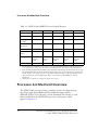
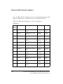
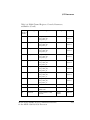
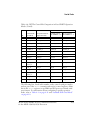
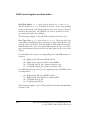
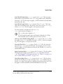
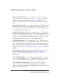
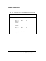
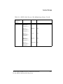
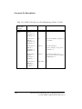
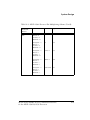
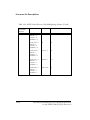
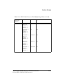
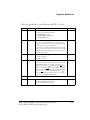
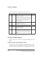
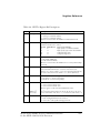
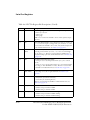
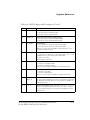
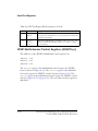
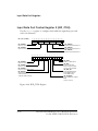
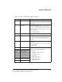
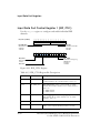
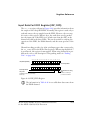
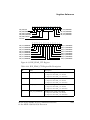
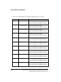
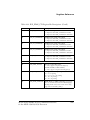
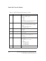
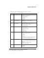
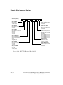
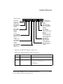
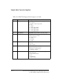
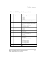
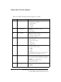
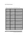
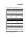
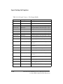
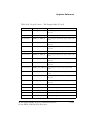
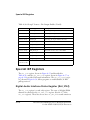
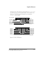
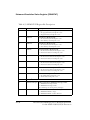
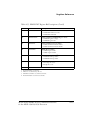
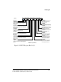
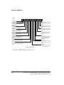
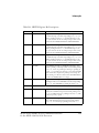
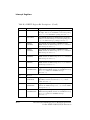
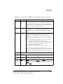
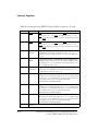
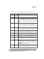
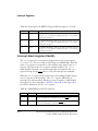
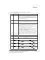
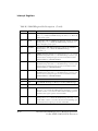
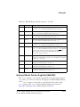
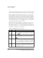
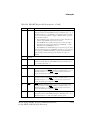
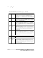
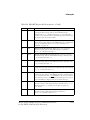
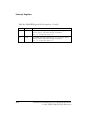
• “Processor Pin Descriptions” on page 12-2
• “Phase-Locked Loop Start Up” on page 12-27
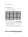
• “Conditioning Input Signals” on page 12-28
• “Designing for High Frequency Operation” on page 12-29
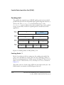
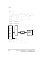
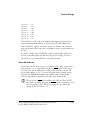
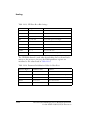
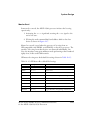
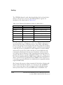
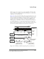
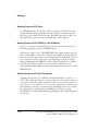
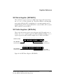
• “Booting” on page 12-34
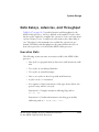
• “Data Delays, Latencies, and Throughput” on page 12-49
Other chapters also discuss system design issues. Some other locations for
system design information include:
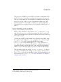
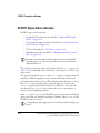
• “SPORT Operation Modes” on page 4-10
• “SPI General Operations” on page 5-8
By following the guidelines described in this chapter, you can ease the
design process for your ADSP-2136x processor product. Development
and testing of your application code and hardware can begin without
debugging the JTAG port.
ADSP-2136x SHARC Processor Hardware Reference
for the ADSP-21362/3/4/5/6 Processors
12-1