1
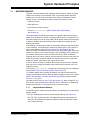
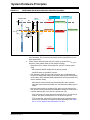
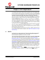
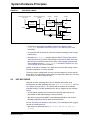
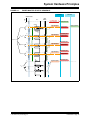
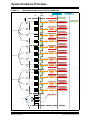
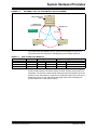
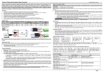
System Hardware Principles • All user-created sockets are automatically destroyed. • INIC asserts RSOUT pin to reset the EHC (requirement in this system). Since the EHC is reset, it must recover from this situation under all conditions. If the watchdog is triggered in any network slave device (does not contain the NWM), the INIC also sends an empty FBlock list to the network master indicating its FBlocks are no longer available: 0x0400: NetBlock.InstID.FBlockIDs.Status() If the watchdog is triggered in the network master device (HU), then INIC broadcasts the message: 0x03C8: NWM.InstID.Configuration.Status(NotOK) In addition, since the HU also contains the power master, INIC will shutdown the network after INIC.InstID.WatchdogMode.AutoShutDownDelay expires, unless the power master EHC re-attaches to INIC before then. 4.3 NETWORK PHYSICAL LAYER All devices shall comply with the MOST Electrical Physical Layer Specification [10]. In the device, the PCB layout of the INIC network signal and front end routing is critical to achieving a clean, low-jitter network which meets OEM EMC requirements. Layout guidelines for INIC and the network signals are provided in the OS81092 INIC Hardware Data Sheet [7]. In addition, all devices shall utilize Microchip’s free MOSTCheck™ schematic and layout review service to ensure the best possible network performance. As required in the MOST Electrical Physical Layer Specification [10], all PCB designs must provide clean access to the physical layer specification points. For the electrical PHY, the four points are SP1E, SP2E, SP3E, and SP4E. While the SP2E and SP3E points could be accessed through the harness connector, the SP1E and SP4E points require test points on the PCB (ideally all four points would be available on the PCB). These test points should be routed such that integrity of the differential pair is maintained and stubs are avoided. For best results, the test points should be placed directly in-line with the differential traces and located at the far end of the transmission line. Two examples of test point placement are illustrated in Figure 4-2. FIGURE 4-2: DIFFERENTIAL TEST POINTS Differential Test Points Using Only SMD Pads 2013 Microchip Technology Inc. Differential Test Points Using 100 Mil Header DS20005241A-page 23