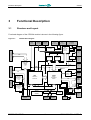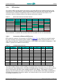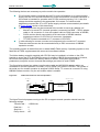
1
CPC304
PC/104-Plus
AMD Geode LX 800 Based
Processor Module
User Manual
Rev. 003a E
November 2011
Product Title:
Document name:
Manual version:
Ref. doc. v.:
CPC304
CPC304 User Manual
003a E
1.5 R (467444.013)
Copyright © 2008, 2009, 2010, 2011 Fastwel Co. Ltd. All rights reserved.
Revision Record
Rev. Index
Brief Description of Changes
Board Index
Date of Issue
001
Initial preliminary version
CPC304
January 2008
001a
Delivery checklist corrected, document structure changed
CPC304
August 2008
002
BIOS Setup chapter added, Block diagram and board layout diagram
corrected, all chapters reworked
CPC304
June 2009
003
Changes mainly following the release of v.1.3 of the module. BIOS Setup
section changed; DDMA programming added; BIOS upgrade section
revised; several illustrations added or corrected, multiple text changes
CPC304
July 2010
003a
J17 (TFT) pinout corrected
CPC304
November 2011
Contact Information
Fastwel Co. Ltd
Fastwel Corporation US
Address:
108 Profsoyuznaya st.,
Moscow 117437,
Russian Federation
45 Main Street, Suite 319
Brooklyn, New York 11201
USA
Tel.:
+7 (495) 232-1681
+1 (718) 554-3686
Fax:
+7 (495) 232-1654
+1 (718) 797-0600
Toll free:
E-mail:
[email protected]
Web:
http://www.fastwel.com/
+1 (877) 787-8443 (1-877-RURUGGED)
CPC304
Table of Contents
Table of Contents ..............................................................................................................................................1
List of Tables .....................................................................................................................................................3
List of Figures ....................................................................................................................................................4
Notation Conventions.........................................................................................................................................5
General Safety Precautions................................................................................................................................6
Unpacking, Inspection and Handling...................................................................................................................7
Three Year Warranty..........................................................................................................................................8
1
Introduction...................................................................................................................................... 9
1.1
1.2
1.3
1.4
1.5
2
Technical Specifications.................................................................................................................13
2.1
2.2
2.3
2.4
2.5
2.6
3
Module Introduction.................................................................................................................................9
CPC304 Versions..................................................................................................................................10
Delivery Checklist..................................................................................................................................11
Additional Accessories ..........................................................................................................................11
Supplementary Information....................................................................................................................12
1.5.1
Related Documents...............................................................................................................12
General.................................................................................................................................................13
Power Requirements.............................................................................................................................15
Environmental.......................................................................................................................................15
Mechanical ...........................................................................................................................................15
Dimensions and Weight.........................................................................................................................15
MTBF ...................................................................................................................................................15
Functional Description ...................................................................................................................16
3.1
3.2
CP C3 0 4
Structure and Layout .............................................................................................................................16
Functional Description...........................................................................................................................19
3.2.1
Microprocessor .....................................................................................................................19
3.2.2
SDRAM Memory...................................................................................................................19
3.2.3
Reserved Flash BIOS ...........................................................................................................19
3.2.4
IDE Interface.........................................................................................................................20
3.2.4.1
Connection of External IDE Devices ......................................................................20
3.2.4.2
CompactFlash Socket ...........................................................................................21
3.2.4.3
NAND Flash .........................................................................................................22
3.2.5
Video Controller and Connection of Monitors .........................................................................23
3.2.6
Fast Ethernet Interface..........................................................................................................26
3.2.7
USB Interface .......................................................................................................................27
3.2.8
FDD/LPT Port .......................................................................................................................27
3.2.9
Serial Ports...........................................................................................................................28
3.2.9.1
COM1 and COM2 (RS232) ...................................................................................28
3.2.9.2
COM3 and COM4 (RS485/RS422) ........................................................................29
3.2.10
PS/2 Keyboard and Mouse Interface......................................................................................31
3.2.11
Audio Port.............................................................................................................................32
3.2.12
Optoisolated Reset/IRQ Input................................................................................................32
3.2.13
RTC and CMOS + Serial FRAM ............................................................................................33
3.2.14
Watchdog Timers..................................................................................................................33
3.2.15
J25 Pinpad ...........................................................................................................................33
3.2.16
J26 Pinpad ...........................................................................................................................34
Us e r
M a n u a l
1
© 2 0 1 1
F a s t w e l
v . 0 0 3 a
E
CPC304
3.2.17
3.2.18
3.2.19
3.2.20
3.2.21
3.2.22
3.2.23
J28 Pinpad ...........................................................................................................................34
Discrete Input/Output ............................................................................................................35
External PME Signal Connector.............................................................................................35
Battery Connector .................................................................................................................36
Diagnostic LEDs ...................................................................................................................36
Reset Button.........................................................................................................................37
Expansion Buses: ISA and PCI .............................................................................................38
3.2.23.1 ISA Header...........................................................................................................38
3.2.23.2 PCI Header...........................................................................................................40
3.2.24
Power Supply .......................................................................................................................41
Address Mapping ..................................................................................................................................42
3.3.1
Memory Addressing ..............................................................................................................42
3.3.2
I/O Addressing......................................................................................................................43
3.3.3
Interrupt settings ...................................................................................................................44
3.3.4
DMA Channels......................................................................................................................44
Overall and Mounting Dimensions .........................................................................................................45
3.3
3.4
4
External Connections .....................................................................................................................46
4.1
4.2
Safety Regulations ................................................................................................................................46
Connection of Peripheral Devices ..........................................................................................................47
4.2.1
CompactFlash Cards Installation ...........................................................................................49
4.2.2
USB Devices Connection ......................................................................................................49
4.2.3
Battery Replacement.............................................................................................................49
Software Installation..............................................................................................................................49
4.3
5
General Software® BIOS ................................................................................................................50
5.1
5.2
5.3
5.4
5.5
5.6
5.7
5.8
5.9
5.10
6
BIOS Setup Program. Introduction.........................................................................................................50
Main Menu............................................................................................................................................50
Basic CMOS configuration.....................................................................................................................52
Features Configuration ..........................................................................................................................54
Custom Configuration............................................................................................................................55
CPC304 Specific Configuration..............................................................................................................58
PnP Configuration.................................................................................................................................58
Shadow Configuration ...........................................................................................................................59
The Rest Main Menu Commands...........................................................................................................59
5.9.1
Start RS232 Manufacturing Link ............................................................................................59
5.9.2
Reset CMOS to Last Known Values ......................................................................................60
5.9.3
Reset CMOS to Factory Defaults...........................................................................................60
5.9.4
Write to CMOS and Exit ........................................................................................................60
5.9.5
Exit without Changing CMOS ................................................................................................61
Extended BIOS Functions .....................................................................................................................61
5.10.1
ADM706T Supervisor Chip-Based Watchdog Timer Control ...................................................61
5.10.1.1 Using INT 17H BIOS Extension to Control the Watchdog Timer..............................61
5.10.2
SMI Control ..........................................................................................................................62
5.10.3
FRAM Memory Access..........................................................................................................62
5.10.4
User LEDs Control ................................................................................................................63
5.10.5
RS 422/485 Transmitters Control (Ports COM3, COM4).........................................................64
5.10.6
Programming of DDMA Controller of IT8888G Bridge.............................................................65
Basic Software ................................................................................................................................69
6.1
6.2
6.3
6.4
CP C3 0 4
Supplied Software.................................................................................................................................69
Reset CMOS to Factory Defaults from a Remote PC..............................................................................69
BIOS Upgrade ......................................................................................................................................70
Manufacturing Link Mode ......................................................................................................................73
Us e r
M a n u a l
2
© 2 0 1 1
F a s t w e l
v . 0 0 3 a
E
CPC304
7
Appendices .....................................................................................................................................74
7.1
Jumper Settings by Function .................................................................................................................74
List of Tables
Table 1.1:
Table 1.2:
Table 1.3:
Table 1.4:
Table 3.1:
Table 3.2:
Table 3.3:
Table 3.4:
Table 3.5:
Table 3.6:
Table 3.7:
Table 3.8:
Table 3.9:
Table 3.10:
Table 3.11:
Table 3.12:
Table 3.13:
Table 3.14:
Table 3.15:
Table 3.16:
Table 3.17:
Table 3.18:
Table 3.19:
Table 3.20:
Table 3.21:
Table 3.22:
Table 3.23:
Table 3.24:
Table 3.25:
Table 3.26:
Table 3.27:
Table 3.28:
Table 5.1:
Table 5.2:
Table 5.3:
Table 5.4:
Table 5.5:
Table 5.6:
Table 5.7:
Table 5.8:
Table 7.1:
CP C3 0 4
Us e r
CPC304 Versions.......................................................................................................................10
CPC304 Supplied Set.................................................................................................................11
CPC304 Additional Accessories..................................................................................................11
Related Publications...................................................................................................................12
IDE Channel: Devices Connection Variants.................................................................................20
J19 HDD Connector Pinout.........................................................................................................20
J20 CompactFlash Socket Pinout................................................................................................21
TFT: J17 Header Pinout..............................................................................................................23
LVDS: J16 Connector Pinout ......................................................................................................25
VGA: J18 Connector Pinout ........................................................................................................26
J4 Ethernet Header Pinout..........................................................................................................26
J21 Connector Pinout .................................................................................................................27
LPT/FDD J23 Connector Pinout ..................................................................................................27
J14 and J15 Pin Assignments .....................................................................................................29
J11 and J13 Contact Assignments ..............................................................................................31
J7 Contacts Designation .............................................................................................................31
Audio: J9 and J8 Pinouts ............................................................................................................32
J25 Jumpers Positions................................................................................................................33
J26 Jumper Positions .................................................................................................................34
J28 Jumpers Positions................................................................................................................34
J5 Contacts Designation .............................................................................................................35
J6 PME Connector Pinout...........................................................................................................35
J3 Battery Connector Pinout .......................................................................................................36
CPC304 Diagnostic LEDs Function.............................................................................................36
J30 External LEDs Connector.....................................................................................................37
ISA P/J1 Connector (Rows A and B) Contacts Designation..........................................................38
ISA P/J1 (Rows C and D) Contacts Designation ..........................................................................39
PCI P/J2 Connector Contacts Designation ..................................................................................40
J24 Power Connector Pinout.......................................................................................................41
Memory Address Mapping ..........................................................................................................42
I/O Address Space .....................................................................................................................43
Interrupt Settings........................................................................................................................44
Main Menu Items........................................................................................................................51
Basic CMOS Configuration Menu Items ......................................................................................53
Features Configuration Menu Items ............................................................................................54
Custom Configuration Menu Items ..............................................................................................55
CPC304 Specific Configuration Menu Item ..................................................................................58
CPC304 DDMA Channels Base Addresses .................................................................................65
DDMA Controller Data Registers.................................................................................................65
Legacy DMA Page Register Addresses.......................................................................................66
Jumper Settings by Function.......................................................................................................74
M a n u a l
3
© 2 0 1 1
F a s t w e l
v . 0 0 3 a
E
CPC304
List of Figures
Figure 1.1:
Figure 3.1:
Figure 3.2:
Figure 3.3:
Figure 3.4:
Figure 3.5:
Figure 3.6:
Figure 3.7:
Figure 3.8:
Figure 3.9:
Figure 3.10:
Figure 3.11:
Figure 3.12:
Figure 3.13:
Figure 3.14:
Figure 3.15:
Figure 3.16:
Figure 4.1:
Figure 4.2:
Figure 5.1:
Figure 5.2:
Figure 5.3:
Figure 5.4:
Figure 5.5:
Figure 5.6:
CPC304 Module Appearance......................................................................................................10
CPC304 Block Diagram..............................................................................................................16
Top Side: Connectors and Main Components Layout...................................................................18
Bottom Side: Connectors and Main Components Layout..............................................................19
Connection of Sharp LQ104V1DG61 Panel to CPC304 ...............................................................24
Connection of Sharp LQ150X1LW72 Panel to CPC304 ...............................................................25
J21 IDC10 Pins Numbering.........................................................................................................27
IDC10 Pins Numbering ...............................................................................................................28
J10 and J12 Pinpads ..................................................................................................................29
Point-to-Point Connection of Two Modules in RS422 Mode..........................................................30
Connection of Several Devices in RS485 Mode...........................................................................30
Discrete Input Optoisolation........................................................................................................32
External LEDs Connection..........................................................................................................37
ISA Header Contacts Layout.......................................................................................................38
PCI P/J2 Connector Contacts Layout ..........................................................................................40
J24 Power Supply Connector......................................................................................................41
CPC304: Overall and Mounting Dimensions................................................................................45
External Devices Connection ......................................................................................................47
Cables Connection for Console Operation...................................................................................48
Main Menu Screen Image...........................................................................................................51
Basic CMOS Configuration Screen Image...................................................................................52
Features Configuration Menu Screen ..........................................................................................54
Custom Configuration Menu Screen............................................................................................55
Plug-n-Play Configuration Menu Screen Image ...........................................................................58
Shadow Configuration Menu Screen Image.................................................................................59
All information in this document is provided for reference only, with no warranty of its suitability for any specific purpose. This information has been thoroughly checked and
is believed to be entirely reliable and consistent with the product that it describes. However, Fastwel accepts no responsibility for inaccuracies, omissions or their
consequences, as well as liability arising from the use or application of any product or example described in this document.
Fastwel Co. Ltd. reserves the right to change, modify, and improve this document or the products described in it, at Fastwel's discretion without further notice. Software
described in this document is provided on an “as is” basis without warranty. Fastwel assumes no liability for consequential or incidental damages originated by the use of
this software.
This document contains information, which is property of Fastwel Co. Ltd. It is not allowed to reproduce it or transmit by any means, to translate the document or to convert
it to any electronic form in full or in parts without antecedent written approval of Fastwel Co. Ltd. or one of its officially authorized agents.
Fastwel and Fastwel logo are trademarks owned by Fastwel Co. Ltd., Moscow, Russian Federation. Ethernet is a registered trademark of Xerox Corporation. IEEE is a
registered trademark of the Institute of Electrical and Electronics Engineers Inc. Intel is a trademark of Intel Corporation. Geode is trademark of AMD. Microsoft is a
trademark of the Microsoft corporation. In addition, this document may include names, company logos and trademarks, which are registered trademarks and, therefore,
are property of their respective owners.
Fastwel welcomes suggestions, remarks and proposals regarding the form and the content of this Manual.
CP C3 0 4
Us e r
M a n u a l
4
© 2 0 1 1
F a s t w e l
v . 0 0 3 a
E
CPC304
Notation Conventions
Warning, ESD Sensitive Device!
This symbol draws your attention to the information related to electro static sensitivity of your
product and its components. To keep product safety and operability it is necessary to handle
it with care and follow the ESD safety directions.
Warning!
This sign marks warnings about hot surfaces. The surface of the heatsink and some
components can get very hot during operation. Take due care when handling, avoid
touching hot surfaces!
Caution: Electric Shock!
This symbol warns about danger of electrical shock (> 60 V) when touching products or
parts of them. Failure to observe the indicated precautions and directions may expose your
life to danger and may lead to damage to your product.
Warning!
Information marked by this symbol is essential for human and equipment safety.
Read this information attentively, be watchful.
Note...
This symbol and title marks important information to be read attentively for your own benefit.
CP C3 0 4
Us e r
M a n u a l
5
© 2 0 1 1
F a s t w e l
v . 0 0 3 a
E
CPC304
General Safety Precautions
This product was developed for fault-free operation. Its design provides conformance to all related
safety requirements. However, the life of this product can be seriously shortened by improper
handling and incorrect operation. That is why it is necessary to follow general safety and
operational instructions below.
Warning!
All operations on this device must be carried out by sufficiently
skilled personnel only.
Warning!
When handling this product, special care must be taken not to hit
the heatsink (if installed) against another rigid object. Also, be
careful not to drop the product, since this may cause damage
to the heatsink, CPU or other sensitive components as well.
Please, keep in mind that any physical damage to this product
is not covered under warranty.
Note:
This product is guaranteed to operate within the published
temperature ranges and relevant conditions. However, prolonged
operation near the maximum temperature is not recommended by
Fastwel or by electronic chip manufacturers due to thermal stress
related failure mechanisms. These mechanisms are common to all
silicon devices, they can reduce the MTBF of the product by
increasing the failure probability. Prolonged operation at the lower
limits of the temperature ranges has no limitations.
Caution, Electric Shock!
Before installing this product into a system and before installing
other devices on it, always ensure that your mains power is switched
off.
Always disconnect external power supply cables during all handling
and maintenance operations with this module to avoid serious
danger of electrical shock.
CP C3 0 4
Us e r
M a n u a l
6
© 2 0 1 1
F a s t w e l
v . 0 0 3 a
E
CPC304
Unpacking, Inspection and Handling
Please read the manual carefully before unpacking the module or mounting the device into your
system. Keep in mind the following:
ESD Sensitive Device!
Electronic modules and their components are sensitive to static
electricity. Even a non-perceptible by human being static discharge
can be sufficient to destroy or degrade a component's operation!
Therefore, all handling operations and inspections of this product
must be performed with due care, in order to keep product integrity
and operability:
n
Preferably, unpack or pack this product only at EOS/ESD safe workplaces. Otherwise, it is
important to be electrically discharged before touching the product. This can be done by
touching a metal part of your system case with your hand or tool. It is particularly important
to observe anti-static precautions when setting jumpers or replacing components.
If the product contains batteries for RTC or memory back-up, ensure that the module is not
placed on conductive surfaces, including anti-static mats or sponges. This can cause shortcircuit and result in damage to the battery and other components.
Store this product in its protective packaging while it is not used for operational purposes.
n
n
Unpacking
The product is carefully packed in an antistatic bag and in a carton box to protect it against
possible damage and harmful influence during shipping. Unpack the product indoors only at a
temperature not less than +15°C and relative humidity not more than 70%. Please note, that if the
product was exposed to the temperatures below 0°С for a long time, it is necessary to keep it at
normal conditions for at least 24 hours before unpacking. Do not keep the product close to a heat
source.
Following ESD precautions, carefully take the product out of the shipping carton box. Proper
handling of the product is critical to ensure correct operation and long-term reliability. When
unpacking the product, and whenever handling it thereafter, be sure to hold the module preferably
by the front panel, card edges or ejector handles. Avoid touching the components and connectors.
Retain all original packaging at least until the warranty period is over. You may need it for
shipments or for storage of the product.
Initial Inspection
Although the product is carefully packaged, it is still possible that shipping damages may occur.
Careful inspection of the shipping carton can reveal evidence of damage or rough handling. Should
you notice that the package is damaged, please notify the shipping service and the manufacturer
as soon as possible. Retain the damaged packing material for inspection.
After unpacking the product, you should inspect it for visible damage that could have occurred
during shipping or unpacking. If damage is observed (usually in the form of bent component leads
or loose socketed components), contact Fastwel's official distributor from which you have
purchased the product for additional instructions. Depending on the severity of the damage, the
product may even need to be returned to the factory for repair. DO NOT apply power to the product
if it has visible damage. Doing so may cause further, possibly irreparable damage, as well as result
in a fire or electric shock hazard.
If the product contains socketed components, they should be inspected to make sure they are
seated fully in their sockets.
CP C3 0 4
Us e r
M a n u a l
7
© 2 0 1 1
F a s t w e l
v . 0 0 3 a
E
CPC304
Handling
In performing all necessary installation and application operations, please follow only the
instructions supplied by the present manual.
In order to keep Fastwel’s warranty, you must not change or modify this product in any way, other
than specifically approved by Fastwel or described in this manual.
Technical characteristics of the systems in which this product is installed, such as operating
temperature ranges and power supply parameters, should conform to the requirements stated by
this document.
Retain all the original packaging, you will need it to pack the product for shipping in warranty cases
or for safe storage. Please, pack the product for transportation in the way it was packed by the
supplier.
When handling the product, please, remember that the module, its components and connectors
require delicate care. Always keep in mind the ESD sensitivity of the product.
Three Year Warranty
Fastwel Co. Ltd. (Fastwel), warrants that its standard hardware products will be free from defects
in materials and workmanship under normal use and service for the currently established warranty
period. Fastwel’s only responsibility under this warranty is, at its option, to replace or repair any
defective component part of such products free of charge.
Fastwel neither assumes nor authorizes any other liability in connection with the sale, installation
or use of its products. Fastwel shall have no liability for direct or consequential damages of any
kind arising out of sale, delay in delivery, installation, or use of its products.
If a product should fail through Fastwel's fault during the warranty period, it will be repaired free of
charge. For out of warranty repairs, the customer will be invoiced for repair charges at current
standard labor and materials rates.
Warranty period for Fastwel products is 36 months since the date of purchase.
The warranty set forth above does not extend to and shall not apply to:
1.
Products, including software, which have been repaired or altered by other than
Fastwel personnel, unless Buyer has properly altered or repaired the products in
accordance with procedures previously approved in writing by Fastwel.
2.
Products, which have been subject to power supply reversal, misuse, neglect,
accident, or improper installation.
Returning a product for repair
1.
Apply to Fastwel company or to any of the Fastwel's official representatives for the
Product Return Authorization.
2.
Attach a failure inspection report with a product to be returned in the form, accepted by
customer, with a description of the failure circumstances and symptoms.
3.
Carefully package the product in the antistatic bag, in which the product had been
supplied. Failure to package in antistatic material will VOID all warranties. Then
package the product in a safe container for shipping.
4.
The customer pays for shipping the product to Fastwel or to an official Fastwel
representative or dealer.
CP C3 0 4
Us e r
M a n u a l
8
© 2 0 1 1
F a s t w e l
v . 0 0 3 a
E
Introduction
1
CPC304
Introduction
This document presents general information on CPC304 processor module, the details of its
proper and safe installation, configuration and operation. The issues of PC/104 modules and
external devices connection are also considered.
1.1
Module Introduction
CPC304 is a PC/104-Plus single board computer for embedded applications. It is designed for use
in mission critical on-board systems requiring low power consumption and wide operating
temperature range. CPC304 is based on AMD Geode LX800 CPU and AMD CS5536 I/O
companion. CPC304 provides full support for PC/104 and PC/104-Plus expansion modules and
data exchange via both 16-bit ISA and 32-bit PCI buses.
All key components including CPU, chipset, memory, and periphery controllers are soldered onboard providing excellent vibration stability and increased efficiency of protective conformal
coating.
CPC304 offers wide variety of data display capabilities. It allows simultaneous operation of
standard VGA interface, 24-bit LVDS interface, and 18-bit interface for TFT or DSTN LCD panels
connection.
Data storage subsystem is based on single-channel IDE controller, that is able to drive two IDE
devices: two external hard drives connected via on-board connectors, CompactFlash card, or
soldered on-board 1 GB flash disk.
For data exchange, CPC304 uses up to two independent Fast Ethernet ports, up to four COM
ports, two USB 2.0 ports, and eight programmable discrete input/output lines.
System control and management capabilities of CPC304 include two watchdog timers, optoisolated remote Reset/IRQ input, external signal system wake-up controller, reserved BIOS, and
possibility to save system configuration and emergency parameters in FRAM chip.
CPC304 is designed for operation within industrial temperature range from –40°C to +85°C.
CPC304 is manufactured in three versions: CPC30401, full function version, CPC30402,
"light-weight" version without LVDS interface and on-board 1 GB NAND flash disk, with one
Fast Ethernet channel and three COM ports. CPC30403 is a variant of CPC30401 Coated version
with extended operating temperature range.
CPC304 is supplied with the preinstalled FDOS 6.22 operating system and supports MS DOS,
Windows CE5.0, CE6.0, XPe, as well as QNX 6.3x, and Linux 2.6 operating systems.
CP C3 0 4
Us e r
M a n u a l
9
© 2 0 1 1
F a s t w e l
v . 0 0 3 a
E
Introduction
CPC304
Figure 1.1:
CPC304 Module Appearance
The appearance may vary for different versions of the module.
1.2
CPC304 Versions
At the present time the CPC304 module is manufactured in three basic versions differing in
interface capabilities and coating. In this Manual the notes related to the CPC30401 and
CPC30402 basic versions apply to their coated variants as well. The version “CPC30403 Coated”
is a variant of CPC30401 with widened operating temperature range and protective coating.
Table 1.1:
CPC304 Versions
Version
T Range
LVDS
NAND Flash
Ethernet
RS422/485
Coating
+
+
2
COM3, COM4
–
+
+
2
COM3, COM4
+
CPC30402
–
–
1
COM3
–
CPC30402 Coated
–
–
1
COM3
+
+
+
2
COM3, COM4
+
CPC30401
CPC30401 Coated
CPC30403 Coated
CP C3 0 4
Us e r
-40°C to +85°C
-50°C to +85°C
M a n u a l
10
© 2 0 1 1
F a s t w e l
v . 0 0 3 a
E
Introduction
1.3
CPC304
Delivery Checklist
Table 1.2:
CPC304 Supplied Set
Code
Decimal Code
Description
CPC30401
CPC30401 Coated
CPC30402
CPC30402 Coated
CPC30403 Coated
467444.013
467444.013-01
467444.013-02
467444.013-03
467444.013-04
CPC304 processor module
CDM02
469535.023
Adapter module for connection of 3.5" HDD or CD-ROM drive
–
685611.051
Cable for 2.5" HDD connection to 44-contact header
469539.012
Lithium battery assembly (p/n: CR2032/1F4 DART)
ACS00023
685611.082
DB9F to IDC10 adapter cable for connection to COM1 or COM2 ports
–
–
Mounting standoffs kit
–
–
Jumpers set
–
467369.009
CD ROM with documentation and service software
–
–
Antistatic bag and consumer carton box
Note:
Keep the antistatic bag and the original package at least until the warranty period
is over. It can be used for future storage or warranty shipments.
1.4
Additional Accessories
Peripheral devices are attached to the module directly or via additional accessories and cables
listed in the following table. Additional accessories are not supplied with the CPU module, are
ordered separately.
Table 1.3:
CPC304 Additional Accessories
Name
Decimal Code
Description
KIB380
469515.004
Interface expansion module with standard connectors and cable set
ACS00027
685611.123
Adapter cable (IDC10 2 mm – DHS-15F) for connection of VGA monitor
to the module
ACS00031-01
467941.016
PHR-5 connector set. Includes JST PHR-5 socket and a set of contacts
SPH-002T-P0.5S for connection to J9, J11, or J13 headers of the
module
ACS00031-02
467941.016-01
PHR-6 connector set. Includes JST PHR-6 socket and a set of contacts
SPH-002T-P0.5S for connection to J7 header of the module
ACS00031-03
467941.016-02
PHR-2 connector set. Includes JST PHR-2 socket and a set of contacts
SPH-002T-P0.5S for connection to J6 or J8 headers of the module
ACS00037
–
DF13 connector set. Includes Hirose DF13-20DS-1.25C socket and a
set of contacts DF13-2630SCF for connection to J16 header
ACS00038
–
Connector set for connection of a power supply unit to the module.
Includes AMP 4-171822-4 socket and a set of contacts 170263-1 for
connection to J24 power connector of the module
ACS00040-01
–
IDC-10 connector set. Includes Leotronics 2040-3102 socket for
connection to J14, J15, J18, or J21 headers of the module
ACS00040-02
–
IDC-16 connector set. Includes Leotronics 2040-3162 socket for
connection to J4 header
CP C3 0 4
Us e r
M a n u a l
11
© 2 0 1 1
F a s t w e l
v . 0 0 3 a
E
Introduction
CPC304
Name
Decimal Code
Description
ACS00040-03
–
IDC-26 connector set. Includes Leotronics 2040-3262 socket for
connection to J23 header
ACS00041
–
Connector set for diskrete input/output connection (J5). Includes AMP
1-87499-5 socket and 167021-2 contacts.
1.5
Supplementary Information
1.5.1
Related Documents
Information related to this product and its components can be found in the following documents:
Table 1.4:
Related Publications
Product
Publication
CompactFlash cards
CF+ and CompactFlash Specification Revision 1.4
Processor
AMD Geode™ LX Processor Reference Schematic
AMD Geode™ LX Processors Data Book
AMD Geode™ CS5536 Companion Device Preliminary Data Book
AMD Geode™ LX Processor and CS5535/CS5536 Companion Devices
Layout Recommendations
Super I/O
CP C3 0 4
Winbond W83627 SuperIO Data sheet
Us e r
M a n u a l
12
© 2 0 1 1
F a s t w e l
v . 0 0 3 a
E
Technical Specifications
CPC304
2
Technical Specifications
2.1
General
n
n
n
n
n
n
n
n
CP C3 0 4
CPU: AMD Geode LX800 500 MHz:
§
32-bit x86/x87 compatible
§
64-bit coprocessor
§
64-bit memory bus
§
64 KB L1, 128 KB L2 cache
§
Integrated FPU supports the Intel MMX™ and AMD 3DNow!™ Technology
instruction sets
System memory:
§
256 MB soldered DDR SDRAM
§
DDR333
Flash BIOS:
§
2x512 KB, reserved
§
In-system modification
Solid State Disk (except for CPC30402)
§
Soldered
§
1 GB NAND flash
§
IDE interface
§
MS DOS-compatible Fastwel file system
CompactFlash socket:
§
Type I/II cards support (bottom side)
§
DMA mode support
Video controller:
§
2D accelerator
§
Video memory up to 60 MB shared with system
§
LCD (TFT or DSTN) panels support, resolution up to 1024x768 at 60 Hz
§
18-bit color via TFT interface
§
24-bit color via LVDS interface (except for CPC30402)
§
Analog display support,
resolution 1600´1200 at 85 Hz, 1920´1440 at 75 Hz, 32-bit
Ethernet:
§
Two Fast Ethernet ports 10/100 Mbit/s (for CPC30402 – one channel)
USB:
§
Two USB 2.0 channels
§
One device can be connected to each channel
Us e r
M a n u a l
13
© 2 0 1 1
F a s t w e l
v . 0 0 3 a
E
Technical Specifications
n
n
n
n
n
n
n
n
n
n
n
n
n
CP C3 0 4
CPC304
IDE port:
§
One IDE channel (Primary)
§
Support for up to two UltraDMA-100 IDE devices (via a 10 cm cable)
with NAND Flash disabled in BIOS Setup and if the CompactFlash socket (J20)
is not populated
FDD:
§
Floppy disk interface. Header shared with LPT
Parallel port:
§
SPP/ECP/EPP compatible. Header shared with FDD controller
Serial ports:
§
Four serial ports (three for CPC30402)
§
High speed NS16C550 compatible
§
COM1, COM2: RS232, 9 wires (complete), up to 115.2 Kb/s,
console operation support
§
COM3, COM4: RS422/485, 500V isolation, up to 115.2 Kb/s,
FIFO buffer for each channel – 64 bytes (for CPC30402 COM3 only)
PS/2:
§
PS/2 keyboard and mouse interface
AC’97 audio:
§
Stereo Line In and Line Out, microphone input
Remote Reset/IRQ:
§
Discrete remote reset/interrupt input
§
500V optoisolation
RTC:
§
On-board real time clock with Li battery backup
Safety:
§
System configuration settings stored in CMOS+Serial FRAM
§
Possibility of batteryless operation
Two watchdog timers with LED indication:
§
WDT1 with fixed timeout period of 1.6 s
§
WDT2 with programmable timeout period from 1 s to 255 min
Discrete I/O:
§
8 programmable discrete I/O channels
PME:
§
Connector for external PME signal source
Software Support:
§
General Software® BIOS
§
Preinstalled FDOS 6.22 operating system
§
Support for MS DOS, Windows CE5.0, CE6.0, XPe, QNX 6.3x,
and Linux 2.6 operating systems
Us e r
M a n u a l
14
© 2 0 1 1
F a s t w e l
v . 0 0 3 a
E
Technical Specifications
2.2
CPC304
Power Requirements
The module can be powered either via PC/104 ISA bus or via J24 power connector from an
external DC power source providing the following characteristics:
n
n
Voltage: +5 V ±5% (from +4.75 V to +5.25 V)
Consumption current (without external devices): not more than 1.5 A
Important:
+12 V voltage is not used by the module. +12 V line from power
supply connector is routed to the PC/104 header contact.
Please, find important notes on power supply in subsection 3.2.26
of this document.
2.3
Environmental
n
Operating temperature range: from –40°C to +85°C
n
n
Storage temperature: –55°C to +90°C
Relative humidity: up to 80% at 25°С, noncondensing
Note:
Protective coating of CPC304 versions makes them resistant to
damp heat cyclic exposure at temperatures up to +55±2°C and
relative humidity of up to 93±3%.
2.4
Mechanical
n
n
n
2.5
Vibration – 10g;
Single shock, peak acceleration – 150 g;
Multiple shock, peak acceleration – 50 g.
Dimensions and Weight
n
n
2.6
Dimensions, not more: 115.6 × 101.5 × 23.7 mm (4.55” × 4” × 0.93”)
(see also section 4.4 for mounting dimensions)
Weight, not more:
0.2 kg
(without CompactFlash card)
MTBF
n
MTBF for CPC304 is 170000 hours.
The value is calculated according to: Telcordia Issue 1 model, Method I Case 3, for continuous operation
at a surface location, at normal environmental conditions and at ambient temperature 30°С.
CP C3 0 4
Us e r
M a n u a l
15
© 2 0 1 1
F a s t w e l
v . 0 0 3 a
E
Functional Description
CPC304
3
Functional Description
3.1
Structure and Layout
Functional diagram of the CPC304 module is shown in the following figure.
Figure 3.1:
CPC304 Block Diagram
PME
2 pin (J6)
Discrete
In/Out
Opto
RST/IRQ
9 pin (J5)
2 pin (J27)
COM1
COM2
RS232
IDC 10 (J14)
RS232
IDC 10 (J15)
LPT/FDD
IDC 26 (J23)
KBD/MS
6 pin (J7)
LPC
Super I/O
Supervisor
& WDT
W83627
(Winbond)
LVDS
PC/104
16-bit ISA
20 pin
(J16)
ISA
BIOS2
BIOS1
SST49LF008A
SST49LF008A
LVDS
Transmitter
TFT
PCI to ISA
Bridge
LPC
VGA
PME
Reset
PC/104
32-bit PCI
IT8888G
(ITE)
2 pin (J8)
AC97
Codec
ALC203
AMD
Geode LX
Processor
SYS
CS5536
Geode
Companion
Device
IDE
IDC 16 (J4)
Ethernet 1, 2
LU82551IT
(Intel)
Sound
In/Out
5 pin (J9)
IDE
IDC 44
(J19)
CF
(J20)
Ethernet
Controller 2
PCI
LU82551IT
(Intel)
IDE
to NF
DDR SDRAM
256 MB
CP C3 0 4
VGA
IDC 10
(J18)
Mic
Buzzer
PCI
Ethernet
Controller 1
TFT
18-bit,
30 pin
(J17)
Us e r
RS422/485
Transceiver
RS422/485
Transceiver
USB1
USB2
FM24CL64
Ext LED
COM3
COM4
Connector
8 pin (J30)
RS422/485
5 pin (J11)
RS422/485
5 pin (J13)
M a n u a l
FRAM
16
NAND Flash
1 GB
IDC 10
(J21)
Battery
2 pin (J3)
© 2 0 1 1
F a s t w e l
v . 0 0 3 a
E
Functional Description
CPC304
CPC304 includes the following main functional units:
n
n
n
n
n
n
n
n
n
n
n
n
n
n
n
n
n
n
n
n
n
n
AMD Geode LX 800 500 MHz microprocessor, including 32-bit x86 core, 64-bit
coprocessor, 64-bit SDRAM memory bus;
256 MB soldered DDR SDRAM system memory;
Flash memory based reserved BIOS, in-system modification; 2×512 KB
Onboard NAND flash-disk, 1 GB (CPC30401 and -03 only);
CompactFlash socket (J20);
Integrated graphics controller:
§
Video memory up to 60 MB, shared with system;
§
LCD (TFT or DSTN) panels support, resolution up to 1024´768 (J17);
§
Analog RGB display support (J18);
§
LVDS interface (J16, CPC30401 and -03 only)
Two Fast Ethernet channels 10/100 Mbit/s (J4, CPC30402 has one channel);
Two USB 2.0 channels (J21);
IDE port with support for up to two UltraDMA/100 devices (J19);
FDD/LPT shared header (J23);
Serial ports:
§
COM1 (J14), COM2 (J15): RS232;
§
COM3 (J11), СОМ4 (J13, CPC30401 and -03 only): RS422/RS485;
PS/2 keyboard/mouse port (J7);
Audio port (J8, J9)
Optoisolated remote Reset/interrupt input (J27)
Real time clock with Li battery backup;
CMOS+SFRAM for BIOS configuration storage;
Two watchdog timers;
Eight digital I/O lines (J5);
External PME signal connector (J6);
Lithium battery connector (J3);
PC/104 (ISA) and PC/104-Plus (PCI) expansion connectors
External power connector (J24)
Layouts of main CPC304 components and connectors on top and bottom sides are presented in
Figures 3.2 and 3.3 respectively.
Some external devices can be connected to the module using KIB380 interface expansion module.
KIB380 is equipped with standard connectors giving access to audio port, two RS232 and two
RS422/485 ports, VGA, LPT, PS/2 keyboard and mouse, two Ethernet ports, and two USB ports.
KIB380 is not supplied with the module; it is ordered separately.
External connections are illustrated in Chapter 4.
CP C3 0 4
Us e r
M a n u a l
17
© 2 0 1 1
F a s t w e l
v . 0 0 3 a
E
Functional Description
Figure 3.2:
CPC304
Top Side: Connectors and Main Components Layout
J17
TFT (
18-bit 18)
(J
VGA
)
)
2 (J15 4)
COM
(J27)
5)
1 (J1
M
O
ol (J2
et/IRQ
C
tr
s
n
e
o
R
C
ote
W DT
d Re m
Isolate OM3 (J11)
)
C
4 (J13
COM
(J8)
Mic In
t (J9)
In/Ou
Audio
1)
n (D1 )
, Gree
2
LED1 Green (D1
,
2
D
E
L
J2)
CI (P/
2-bit P
3
s
lu
4-P
CPU
PC/10
e LX
Geod
AMD
( D2 7 )
ellow D20)
Y
r,
e
ge (
Trigg
WDT E Act, Oranzer (BZ1)
ID
Buz n (D1)
e
t, Gre n (D6)
et1 Ac
ee
Ethernet2 Act, Gr
Ethern
(D26)
ellow
)
een&Y tton (SW1
r
G
,
LA N1
r LED
et Bu
e
s
e
w
o
R
P
(J4)
et 1, 2
n
r
L A N2
Ethe
21)
1, 2 (J (J26)
U SB
tor
c
le
Se
Mode
CF/NF
tors
rmina
22 Te
/4
5
8
4
RS
J12)
8)
(J10&
de (J2
u t Mo
p
In
te
Discre
6)
J
(
P ME
)
BIOS
ut (J5
te In/O
re
c
is
D
)
ry (J3
Batte
ridge
A
IS B
PCI to
it ISA
4 16-b
PC/10
(P/J1)
e (J7)
Mous
Kbd &
)
r (J24
P o we
19)
IDE (J
36
CS55
(J23)
D
D
LPT/F
The layout may slightly differ for various versions of the module.
CP C3 0 4
Us e r
M a n u a l
18
© 2 0 1 1
F a s t w e l
v . 0 0 3 a
E
Functional Description
Figure 3.3:
CPC304
Bottom Side: Connectors and Main Components Layout
LVDS
(J16)
AC’97
DD R
M
S DR A
ve
Reser
BIOS
D
Ext LE
)
0
3
(J
I/O
Super
NAND
Flash
sh
actFla
Comp et (J20)
k
Soc
The layout may slightly differ for various versions of the board.
3.2
Functional Description
3.2.1
Microprocessor
The module is based on AMD Geode LX800 microprocessor with 1.8W typical power consumption
at 500 MHz, maximum power 3.6W (TDP). The processor includes 32-bit x86 core, 64-bit
coprocessor and 64-bit DDR memory bus up to 400 MHz, graphics and video controller with VGA
monitors and LCD panels simultaneous operation support. FPU of the processor supports MMX™
and AMD 3DNow!™ technology instruction sets. The CPU is complemented with AMD Geode
CS5536 companion device providing support for numerous I/O functions including IDE, USB,
AC’97 compatible audio, and power management interfaces.
3.2.2
SDRAM Memory
Four DDR 333 SDRAM memory chips are soldered on the bottom side of the PCB. Total memory
size is 256 MB.
3.2.3
Reserved Flash BIOS
The CPC304 takes advantage of flash-memory based BIOS. Two Flash BIOS chips storage
capacity is 512 KB each. The main (working) copy of BIOS occupies 512 KB on a chip in
32-contact PLCC32 panel. Reserve BIOS copy is stored on a soldered chip and is used for
emergency boot. Switching between the main and reserve BIOS copies is performed automatically.
It is possible to upgrade main and reserve copies of BIOS in-system. The procedure is described in
section 6.3.
CP C3 0 4
Us e r
M a n u a l
19
© 2 0 1 1
F a s t w e l
v . 0 0 3 a
E
Functional Description
3.2.4
CPC304
IDE Interface
One-channel IDE controller allows connection of up to two IDE devices (master and slave) and
conforms to ATA-6 specification. Since soldered NAND flash disk uses IDE interface along with
external devices, such as CompactFlash card in a socket or disk drives connected to J19
connector, there is a limited number of the devices connection variants:
Table 3.1:
IDE Channel: Devices Connection Variants
Connection Variant
IDE-Master
IDE-Slave
CF-Master
CF-Slave
NF-Master
NF-Slave
1
+
+
–
–
–
–
2
+
–
–
–
–
+
3
+
–
–
+
–
–
4
–
+
–
–
+
–
5
–
–
–
+
+
–
6
–
+
+
–
–
–
7
–
–
+
–
–
+
The combination (7) marked with red was discovered unstable and is not recommended.
3.2.4.1
Connection of External IDE Devices
IDE channel is routed to J19 connector of CPC304 (Figure 3.2); it is a 44-pin 2 mm pitch header.
Its pinout is shown in the following table. UDMA-100 operation mode is supported with a 10 cm
cable only provided that “Features Configuration -> IDE UDMA” and “Custom Configuration -> IDE
UDMA 5” options are enabled in BIOS Setup.
Table 3.2:
J19 HDD Connector Pinout
Pin#
Signal
Pin#
Signal
Pin#
Signal
Pin#
Signal
1
/RESET
12
DD12
23
/IOW
34
–
2
GND
13
DD2
24
GND
35
DA0
3
DD7
14
DD13
25
/IOR
36
DA2
4
DD8
15
DD1
26
GND
37
/CS1
5
DD6
16
DD14
27
/IOCHRDY
38
/CS3
6
DD9
17
DD0
28
GND
39
DASP
7
DD5
18
DD15
29
/DACK
40
GND
8
DD10
19
GND
30
GND
41
+5V
9
DD4
20
–
31
IRQ
42
+5V
10
DD11
21
DRQ
32
/CS16
43
GND
11
DD3
22
GND
33
DA1
44
–
The cable supplied with the module (685611.051) allows direct connection of a 2.5" HDD to the
J19 connector. Other IDE devices (3.5" HDD, CD-ROM) having 40-contact 2.5 mm pitch connector
can be connected to CPC304 via the CDM02 (469535.023) adapter. This adapter is plugged
directly to the 40-contact connector of the IDE device, and with 685611.051 cable is connected to
CPC304 J19 connector. For custom cables it is recommended to use Leotronics 2040-3442 as
counterpart connector for J19.
CP C3 0 4
Us e r
M a n u a l
20
© 2 0 1 1
F a s t w e l
v . 0 0 3 a
E
Functional Description
3.2.4.2
CPC304
CompactFlash Socket
CompactFlash Type I/II cards can be connected to J20 socket on the bottom side of CPC304. The
device in this socket shares Primary channel with other IDE devices. When CompactFlash socket
is populated, only one more IDE device can be connected to CPC304. CompactFlash device can
operate as Master or Slave (see J26 jumper positions description) and can be designated as
bootable device. The pinout of the J20 socket is presented in the following table.
Table 3.3:
J20 CompactFlash Socket Pinout
Pin #
Function
Pin #
Function
1
GND
26
/CD1
2
D03
27
D11
3
D04
28
D12
4
D05
29
D13
5
D06
30
D14
6
D07
31
D15
7
/CS0
32
/CS1
8
A10 (NC)
33
/VS1
9
/ATA SEL
34
/IORD
10
A09 (NC)
35
/IOWR
11
A08 (NC)
36
/WE
12
A07 (NC)
37
INTRQ
13
VCC (+5V)
38
VCC (+5V)
14
A06 (NC)
39
/CSEL
15
A05 (NC)
40
/VS2
16
A04 (NC)
41
/RESET
17
A03 (NC)
42
IORDY
18
A02
43
/INPACK
19
A01
44
/REG
20
A00
45
/DASP
21
D00
46
/PDIAG
22
D01
47
D08
23
D02
48
D09
24
/IOCS16
49
D10
25
/CD2
50
GND
Note:
(NC) indicates that this contact is not connected to the module's circuits.
Note!
If the module is operated in harsh environment with high vibration
load, it is necessary to make additional arrangements to fix the
CompactFlash card in the socket.
CP C3 0 4
Us e r
M a n u a l
21
© 2 0 1 1
F a s t w e l
v . 0 0 3 a
E
Functional Description
3.2.4.3
CPC304
NAND Flash
The capacity of the soldered on-board NAND flash memory chip is 1 GB (CPC30401 and
CPC30403 only). The generations of the module below 1.3 have 128 MB NAND flash memory with
no UDMA support. This flash drive can be used as a bootable disk or can be disabled in BIOS
Setup. NAND flash disk contains the preinstalled FDOS 6.22 operating system compatible with MS
DOS 6.22 and some software utilities providing operational availability of the module. NAND flash
chip is connected to IDE controller via SM223AT IDE-to-NAND flash bridge and uses a standard
IDE driver. The other operating systems require installation of an appropriate driver, which can be
found on the CD supplied with the module.
Compact Flash and NAND flash operation mode ("master" or "slave") is selected by setting
jumpers at J26 pinpad: 1-2 closed NAND flash Master, CF Slave; 3-4 closed CF Master, NAND
flash Slave. “3-4” is the factory setting.
Note!
For generations of the module below 1.3: In case the NAND flash
chip is not used ("Onboard NAND Flash" option in BIOS setup is set
to "Disable"), the jumper at J26 pinpad should be removed or set to
the position 3-4.
Note!
In case the NAND flash chip is not used ("Onboard Flash Disk"
option in BIOS setup is set to "Disable") it is possible that some
CompactFlash cards will operate only in one mode – Master or
Slave. For correct operation it is necessary to set the required
configuration using J26 jumper switch and settings in “Basic CMOS
Configuration” section of BIOS Setup.
CP C3 0 4
Us e r
M a n u a l
22
© 2 0 1 1
F a s t w e l
v . 0 0 3 a
E
Functional Description
3.2.5
CPC304
Video Controller and Connection of Monitors
The module utilizes graphics controller integrated in Geode LX CPU with the following main
features:
n
Video memory size up to 60 MB shared with system. It is recommended to use 32 MB
as set by default in “Custom Configuration” section of BIOS Setup.
n
Supported resolution up to 1024´768 @ 60 Hz for TFT or DSTN LCD-panels at 18 bpp;
for LVDS (CPC30401 and 03 only) panels – at 24 bpp only;
n
Support of VGA CRT monitors with resolution up to 1600´1200 @ 85 Hz or
1920´1440 @ 75 Hz, 32-bit color
CRT display and LCD panel simultaneous operation
n
TFT LCD panels with color depth of 9, 12, or 18 bits are connected directly to J17 header
(IDC30, 1.27 mm pitch, AMP 1-111196-9 counterpart) of CPC304 using custom interface cable.
The following table presents its pinout.
Table 3.4:
TFT: J17 Header Pinout
Pin#
Signal
Pin#
Signal
1
GND
16
DRGB13 (G3)
2
DOT_CLK
17
DRGB14 (G4)
3
HSYNC
18
DRGB15 (G5)
4
VSYNC
19
GND
5
GND
20
DRGB2 (B0)
6
DRGB18 (R0)
21
DRGB3 (B1)
7
DRGB19 (R1)
22
DRGB4 (B2)
8
DRGB20 (R2)
23
DRGB5 (B3)
9
DRGB21 (R3)
24
DRGB6 (B4)
10
DRGB22 (R4)
25
DRGB7 (B5)
11
DRGB23 (R5)
26
GND
12
GND
27
DISPEN
13
DRGB10 (G0)
28
+3.3V
14
DRGB11 (G1)
29
+3.3V
15
DRGB12 (G2)
30
GND
The figure below illustrates connection of Sharp LQ104V1DG61 panel to CPC304 module.
CP C3 0 4
Us e r
M a n u a l
23
© 2 0 1 1
F a s t w e l
v . 0 0 3 a
E
Functional Description
Figure 3.4:
CPC304
Connection of Sharp LQ104V1DG61 Panel to CPC304
To J17 Connector
of CPC304
To Interface Connector
of LQ104V1DG61 Panel
Signal
Cont
Cont
Signal
GND
DOT_CLK
HSYNC
VSYNC
GND
R0
R1
R2
R3
R4
R5
GND
G0
G1
G2
G3
G4
G5
GND
B0
B1
B2
B3
B4
B5
GND
DISPEN
+3.3V
+3.3V
GND
1
2
3
4
5
6
7
8
9
10
11
12
13
14
15
16
17
18
19
20
21
22
23
24
25
26
27
28
29
30
1
2
3
4
5
6
7
8
9
10
11
12
13
14
15
16
17
18
19
20
21
22
23
24
25
26
27
28
29
30
31
GND
CK
HSYNC
VSYNC
GND
R0
R1
R2
R3
R4
R5
GND
G0
G1
G2
G3
G4
G5
GND
B0
B1
B2
B3
B4
B5
GND
ENAB
VCC
VCC
R/L
U/D
AMP 1-111196-9
Socket
CP C3 0 4
Us e r
M a n u a l
Hirose DF9-31S-1V(32)
Socket
24
© 2 0 1 1
F a s t w e l
v . 0 0 3 a
E
Functional Description
CPC304
J16 connector (Hirose DF13-20DP-1.25V) of CPC304 (CPC30401 and 03 only) is used for
connection of LCD panels to single-channel LVDS interface using custom adapter cable
(counterpart connector Hirose DF13-20DS-1.25C with Hirose DF13-2630SCF contacts) or
using the accessory ACS00037. Only 24-bit panels are supported.
Table 3.5:
LVDS: J16 Connector Pinout
Pin #
Signal
Pin #
Signal
1
VDD_EN
11
TxOUT2+
2
DISPEN
12
TxOUT2-
3
TxOUT0+
13
GND
4
TxOUT0-
14
GND
5
GND
15
TxOUT3+
6
GND
16
TxOUT3-
7
TxOUT1+
17
GND
8
TxOUT1-
18
GND
9
GND
19
TxCLK+
10
GND
20
TxCLK-
Figure 3.5:
Connection of Sharp LQ150X1LW72 Panel to CPC304
+3.3V External Power
To J16 Connector
of CPC304
Signal
VDD_EN
DISPEN
TxOUT0+
TxOUT0GND
GND
TxOUT1+
TxOUT1GND
GND
TxOUT2+
TxOUT2GND
GND
TxOUT3+
TxOUT3GND
GND
TxCLK+
TxCLK-
To Interface Connector
of LQ150X1LW72 Panel
Cont
Cont
Signal
1
2
3
4
5
6
7
8
9
10
11
12
13
14
15
16
17
18
19
20
1
2
3
4
5
6
7
8
9
10
11
12
13
14
15
16
17
18
19
20
VCC
VCC
GND
GND
Rx0Rx0+
GND
Rx1Rx1+
GND
Rx2Rx2+
GND
CKCK+
GND
Rx3Rx3+
GND
GND
Hirose DF13-20DS-1.25C
Socket
CP C3 0 4
Us e r
M a n u a l
Hirose DF14-20S-1.25C
Socket
25
© 2 0 1 1
F a s t w e l
v . 0 0 3 a
E
Functional Description
CPC304
CRT VGA monitor is connected to J18 header (IDC, 2 mm pitch) of CPC304 via a custom adapter
cable (Leotronics 2040-3102 counterpart socket) or using the accessory ACS00040-01. It is also
possible to connect VGA monitor to "VGA" D-Sub connector (J16) of KIB380 interface module. In
this case J18 (CPC304) and J15 (KIB380) headers are connected with the adaptor cable supplied
with KIB380 module. The table below shows J18 header pinout.
Table 3.6:
VGA: J18 Connector Pinout
Pin#
Signal
Pin#
Signal
1
RED
6
GND
2
GND
7
HSYNC
3
GREEN
8
VSYNC
4
GND
9
–
5
BLUE
10
–
3.2.6
Fast Ethernet Interface
The CPC304 has two (one for CPC30402) 10/100Base-T independent Ethernet channels provided
by two Intel LU82551IT controllers. Both Ethernet ports are available via one 16-pin 2 mm pitch
IDC header J4 on the top side of the board (see Figure 3.2). Ethernet channels are connected to
this header via custom adaptor cable with Leotronics 2040-3162 counterpart connector or
ACS00040-02 accessory.
Table 3.7:
J4 Ethernet Header Pinout
Pin Number
Signal
Pin Number
Signal
1
LAN1_TX+
9
LAN2_TX+
2
LAN1_TX-
10
LAN2_TX-
3
LAN1_RX+
11
LAN2_RX+
4
NC
12
NC
5
NC
13
NC
6
LAN1_RX-
14
LAN2_RX-
7
NC
15
NC
8
NC
16
NC
Both channels are available via standard RJ45 connectors on KIB380 interface expansion module.
In this case Ethernet channels are connected directly to J9 (LAN1) and J12 (LAN2) RJ45
connectors of KIB380. J4 CPC304 header is connected to J8 KIB380 header using the adapter
cable supplied with KIB380. Please, refer to the connections diagram in Chapter 4.
CP C3 0 4
Us e r
M a n u a l
26
© 2 0 1 1
F a s t w e l
v . 0 0 3 a
E
Functional Description
3.2.7
CPC304
USB Interface
Figure 3.6:
J21 IDC10 Pins Numbering
The module is equipped with two USB 2.0 host ports.
Each channel has separate power control circuit.
One USB device may be connected to each port.
USB drive boot is supported. Both ports are available via
IDC10 2 mm pitch header J21.
USB devices can be connected to J21 header using a custom
adaptor cable with Leotronics 2040-3102 counterpart connector
or using ACS00040-01 accessory.
Table 3.8:
J21 Connector Pinout
Pin Number
Signal
Pin Number
Signal
1
USB1_+5V
6
USB2_DAT+
2
USB2_+5V
7
USB1_GND
3
USB1_DAT-
8
USB2_GND
4
USB2_DAT-
9
–
5
USB1_DAT+
10
–
USB devices can also be connected to CPC304 via KIB380 interface expansion module,
which has two standard 4-contact Type A USB connectors: USB1 (J4) and USB2 (J5). In this case,
J21 header of CPC304 is connected to J2 header of KIB380 with the adaptor cable supplied with
KIB380. Please, refer to the connections diagram in Chapter 4.
3.2.8
FDD/LPT Port
J23 is a 26-pin 2 mm pitch IDC connector shared by LPT and FDD ports. Switching between LPT
and FDD ports is performed in BIOS Setup. LPT port of CPC304 supports EPP and ECP operation
modes. ECP & EPP 1.7 is the default mode. The operation modes are switched in BIOS Setup.
LPT uses IRQ7 interrupt line, IRQ6 is assigned to FDD port. Interrupts from these ports can be
disabled and switched for use by ISA bus devices in BIOS Setup program.
A floppy disk drive or printer are connected to J23 header of CPC304 via custom cable. The
recommended counterpart connector for J23 is Leotronics 2040-3262 (see ACS00040-03
accessory).
The table below describes pin assignments of J23 connector.
Table 3.9:
LPT/FDD J23 Connector Pinout
Pin #
LPT1 Signals
FDD Signals
1
/STB
–
2
/AFD
DRVDEN
3
PD0
/INDEX
4
/ERROR
/HEAD
CP C3 0 4
Us e r
M a n u a l
27
© 2 0 1 1
F a s t w e l
v . 0 0 3 a
E
Functional Description
CPC304
Pin #
LPT1 Signals
FDD Signals
5
PD1
/TRACK
6
/INIT
/DIR
7
PD2
/WP
8
/SLCTIN
/STEP
9
PD3
/RDATA
10
GND
GND
11
PD4
/DSKCHG
12
GND
GND
13
PD5
–
14
GND
GND
15
PD6
/MOA
16
GND
GND
17
PD7
/DSA
18
GND
GND
19
/ACK
/DSB
20
GND
GND
21
BUSY
/MOB
22
GND
GND
23
PE
/WD
24
GND
GND
25
SLCT
/WE
26
+5V
+5V
A printer can also be connected to DB25F connector (J21) at KIB380 interface expansion module.
The connection between J23 at CPC304 and J20 at KIB380 is made with one of the interface
cables supplied with KIB380 (see the connections diagram in Chapter 4).
3.2.9
Serial Ports
The CPC304-01 and -03 are furnished with four serial ports, CPC304-02 – with three.
3.2.9.1
COM1 and COM2 (RS232)
Figure 3.7:
IDC10 Pins Numbering
COM1 and COM2 ports have standard PC AT base addresses.
They are routed to J14 and J15 IDC10 connectors (2 mm pitch)
respectively and operate as full function 9-wire RS232 interfaces
with maximum transfer rate of 115.2 Kb/s. They are fully compatible
with UART16550.
Both COM1 and COM2 ports can be used for communication with a remote PC; the port number is
selected in BIOS Setup. COM1 is used for this purpose by default. For console operation and file
exchange a null-modem and ACS00023 (685611.082) cables are needed. Recommended
counterpart connectors type for custom cables is Leotronics 2040-3102 (ACS00040-01 accessory).
CP C3 0 4
Us e r
M a n u a l
28
© 2 0 1 1
F a s t w e l
v . 0 0 3 a
E
Functional Description
CPC304
The following table shows pins designation for J14 and J15 headers.
Table 3.10:
J14 and J15 Pin Assignments
Pin #
Signal
Pin #
Signal
1
DCD
2
DSR
3
RXD
4
RTS
5
TXD
6
CTS
7
DTR
8
RI
9
GND
10
+5V
When using KIB380 interface expansion module, both ports are available via two standard DB9F
connectors COM1 (J7) and COM2 (J3). The connection between J14 and J15 at CPC304 and J6
and J1 at KIB380 are made with the interface cables supplied with KIB380 as shown in the
connections diagram in Chapter 4.
3.2.9.2
COM3 and COM4 (RS485/RS422)
COM3 and COM4 ports allow data transmission rates up to 115.2 Kb/s and support RS422/RS485
interfaces with 500 V isolation. They have standard PC/AT base addresses and interrupts. RS485
interface operates in echo mode. These two ports are routed to J11 and J13 one-row 5-pin (JST
type, 2 mm pitch) on-board connectors. CPC30402 version has COM3 only.
The jumpers of the J10 (for COM3) and J12 (for COM4) pinpads connect terminators to
RS485/RS422 signal lines (see table Jumper Settings). The pins of these pinpads have identical
designation shown in the following figure. Pins 1-2 are connected at the factory.
Figure 3.8:
J10 and J12 Pinpads
2
1
4
3
RX-/RX+TerminatorEnabled
TX-/T X+TerminatorEnabled
To use COM3 or COM4 ports in RS422 or RS485 mode, do the following:
§
§
Set jumpers on the pinpad corresponding to the port;
Initialize the port by software
Figure below shows two modules connected in RS422 mode. The jumper connecting terminator is
set on receive lines only (lines RX+ and RX-). In RS485 mode the terminators are connected only
on devices at the ends of the line (on the next figure). The terminators' resistance is 120 Ohm.
CP C3 0 4
Us e r
M a n u a l
29
© 2 0 1 1
F a s t w e l
v . 0 0 3 a
E
Functional Description
Figure 3.9:
CPC304
Point-to-Point Connection of Two Modules in RS422 Mode
J11 / J13
Connector
J10 / J12 [1-2]
J10 / J12 [1-2]
off
off
1
TX+
2
RS-422/RS-485
Converter
120
3
DI
Y
TX+
DE
Z
TX-
4
5
TX+
TX-
TX-
RX+
RX+
RX-
RX-
GND
GND
1
2
RS-422/RS-485
Converter
120
3
4
5
TX+
Y
DI
TX-
Z
DE
RO
A
RX+
RX+
A
RO
H/F
B
RX-
RX-
B
H/F
120
120
J10 / J12 [3-4]
J10 / J12 [3-4]
on
Figure 3.10:
on
Connection of Several Devices in RS485 Mode
Terminating Module
on
RS-422/RS-485
Converter
DI
DE
J10 / J12 [1-2]
120
Y
TX+
Z
TX-
J11 / J13
Connector
1
2
TX+
Peripheral Module
TX-
RO
A
RX+
3
H/F
B
RX
-
4
RX
-
5
GND
RX+
RS-485 Converter
120
RO
off
J10 / J12 [3-4]
D+
DDI
DE
Terminating Module
on
RS-422/RS-485
Converter
Peripheral Module
J10 / J12 [1-2]
J11 / J13
Connector
120
Y
TX+
DE
Z
TX-
RO
A
RX+
4
H/F
B
RX-
5
DI
1
2
3
RS-485 Converter
TX+
TXRO
RX+
RXGND
DI
120
DE
off
J10 / J12 [3-4]
RS422/485 transmitters are controlled via GPIO5 (COM3) and GPIO6 (COM4) lines of CS5536
GPIO port. Setting these lines to logical “1” or “0” switches the tranmitters “on” or “off” respectively.
GPIO lines programming samples can be found in subsection 5.9.5 of this Manual.
Custom cables can be used to connect external devices to RS422/485 interfaces. The
recommended counterpart connectors for J11 and J13 headers of CPC304 are JST PHR-5 with
JST SPH-002T-P0.5S contacts for crimping or ACS00031 accessory.
The following table shows contacts designation for J11 and J13 connectors.
CP C3 0 4
Us e r
M a n u a l
30
© 2 0 1 1
F a s t w e l
v . 0 0 3 a
E
Functional Description
Table 3.11:
CPC304
J11 and J13 Contact Assignments
Pin #
Signal
Pin #
Signal
1
TX+
2
TX-
3
RX+
4
RX-
5
GND
External devices can be connected to RS422/485 interfaces using KIB380 interface expansion
module. The devices are connected to “1 RS 485” (J11) and “2 RS 485” (J14) WAGO terminal
blocks of KIB380. The supplied with KIB380 interface cables are used to connect COM3 (J11)
and COM4 (J13) headers of CPC304 to J10 and J13 connectors of KIB380 respectively. The
connections diagram in Chapter 4 illustrates the wiring layout.
3.2.10
PS/2 Keyboard and Mouse Interface
PS/2 keyboard and mouse interface is routed to J7 6-pin 2 mm pitch JST header. Simultaneous
connection of these two devices to J7 connector of CPC304 require a “Y”-cable purchased
separately.
To make a custom cable it is recommended to use the JST PHR-6 socket with JST SPH-002TP0.5S contacts for crimping (see ACS00031-02 accessory) as a counterpart connector.
The following table shows pinout of CPC304 J7 connector.
Table 3.12:
J7 Contacts Designation
Pin Number
Signal
Pin Number
Signal
1
KBD CLK
4
GND
2
KBD DATA
5
+5V
3
MOUSE CLK
6
MOUSE DATA
Mouse and keyboard can be connected via KIB380 interface expansion module with "KB" and
"Mouse" standard PS/2 connectors (J17 and J19). J7 of CPC304 and J18 of KIB380 are connected
with the cable supplied with KIB380 interface module (see the connections diagram in Chapter 4).
CP C3 0 4
Us e r
M a n u a l
31
© 2 0 1 1
F a s t w e l
v . 0 0 3 a
E
Functional Description
3.2.11
CPC304
Audio Port
The audio port of CPC304 is realized on the basis of AC’97 compatible audio controller supporting
16-bit sound synthesis industry standard and OPL3 mode emulation. External audio devices are
connected to the module via two 2 mm pitch JST connectors: 5-contact J9 (stereo line in/line out)
and 2-contact J8 (microphone in).
For making custom cables it is recommended to use as counterpart connectors JST PHR-5 and
PHR-2 sockets for J9 and J8 headers respectively with JST SPH-002T-P0.5S contacts for crimping
(see ACS00031-01 and ACS00031-03 accessories respectively).
Table 3.13:
Audio: J9 and J8 Pinouts
J9:
J8:
Pin Number
Signal
Pin Number
Signal
1
Lin_In_L
1
Mic_In
2
Lin_In_R
2
GND
3
GND
4
Lin_Out_R
5
Lin_Out_L
Audio devices can also be connected to CPC304 using KIB380 interface module via its standard
3.5 mm audio connectors: Audio In (J24), Audio Out (J26), and Mic (J22). J9 and J8 audio
connectors of CPC304 are connected to J25 and J23 connectors of KIB380 respectively using the
interface cables supplied with KIB380 interface module as shown in the connections diagram in
Chapter 4.
3.2.12
Optoisolated Reset/IRQ Input
J27 is a 2-pin JST 2 mm pitch header that is intended for connection of a remote Reset/IRQ signal
source with voltage of 3 to 5 V. The discrete input has 500 V optoisolation.
Optoisolated Reset circuitry sample is shown in the figure below.
Figure 3.11:
Discrete Input Optoisolation
Optoisolated
Reset Input
S1
E
3-5V
Reset
1
J27
470
2
GND
For making a custom cable it is recommended to use as a counterpart connector JST PHR-2
socket with JST SPH-002T-P0.5S contacts for crimping (see ACS00031-03 accessory).
J28 pinpad is used to switch between the discrete input operation modes: Reset input or IRQ input.
Closing contacts 3-5 and 2-4 enables IRQ input, closing contacts 1-3 (factory setting) enables
Reset input, closing 4-6 enables IRQ on PFO (see Custom Configuration section).
CP C3 0 4
Us e r
M a n u a l
32
© 2 0 1 1
F a s t w e l
v . 0 0 3 a
E
Functional Description
3.2.13
CPC304
RTC and CMOS + Serial FRAM
The module is equipped with a standard Real Time Clock. The supplied with CPC304 3 V lithium
battery assembly is installed in a holder on the processor heatsink. Being connected to J3 power
connector (#1 - +3V, #2 - GND), it is used to power the RTC and CMOS memory when the system
power is off.
FRAM is non-volatile memory with I2C serial interface. It serves as a back-up storage for BIOS
Setup parameters and for restoration of the RTC memory (except the time and date settings) if an
error is detected. This feature enables the possibility to operate the module even when the battery
is disconnected. Free FRAM memory units (7 KB) are available to the user via INT17H BIOS
extensions (see subsection 5.9.3 for details).
For long-term storage of the CPC304 module disconnect RTC battery by disengaging power cable
from J3 connector.
In case of operating system crash and if BIOS Setup program can not be started, BIOS settings
can be reset using CMOS_RST.COM program. It is started under FDOS 6.22 on a remote PC
connected to CPC304 module with a null-modem cable via COM1 port. After this procedure, BIOS
settings are reset to default ones on module's power-up (see section 6.2 for details of the
procedure).
3.2.14
Watchdog Timers
CPC304 has two watchdog timers. WDT1 is integrated in ADM706T supervisor chip and has fixed
timeout period of 1.6 s. After power-up and POST WDT1 is disabled. WDT1 is controlled via INT
17h BIOS extensions and by setting the SuperIO (W83627HG) GPIO port lines; see subsection
5.9.1. WDT1 can induce Reset only if pins 1 and 2 on J25 pinpad are closed (factory setting).
WDT2 is a function of Winbond W83627HG SuperIO chip. It has programmable timeout period
from 1 s to 255 minutes. Its setup and control are described in W83627 chip datasheet
(W83627.pdf file on the CD supplied with CPC304). Super IO chip is available via 2Eh port.
WDT2 can induce Reset only if pins 3 and 4 on J25 pinpad are closed (factory setting).
Operation of each watchdog timer trigger special registers, which are available to BIOS function for
reading after reboot. If SuperIO line GPIO20 is set to logical “1”, WDT operated; to “0” – WDT did
not operate. The fact of watchdog operation is also reflected by lighting D27 yellow LED.
3.2.15
J25 Pinpad
J25 pinpad jumpers allow to enable/disable inducing Reset by watchdog timers of the module.
CPC304 is supplied with pins 1-2 and 3-4 closed. To disable Reset by a watchdog timer remove
the jumper from the appropriate pins.
Table 3.14:
J25 Jumpers Positions
Jumper Position
Function
1-2 closed
Enable Reset from WDT1
3-4 closed
Enable Reset from WDT2
CP C3 0 4
Us e r
M a n u a l
33
© 2 0 1 1
F a s t w e l
v . 0 0 3 a
E
Functional Description
3.2.16
CPC304
J26 Pinpad
Compact Flash and NAND flash operation mode ("master" or "slave") is selected by setting
jumpers at J26 pinpad.
Table 3.15:
J26 Jumper Positions
Jumper Position
Function
3-4
Compact Flash – Master, Nand Flash – Slave (factory setting)
1-2
Compact Flash – Slave, Nand Flash – Master
Note!
For generations of the module below 1.3: In case the NAND flash
chip is not used ("Onboard NAND Flash" option in BIOS setup is set
to "Disable"), the jumper at J26 pinpad should be removed or set to
the position 3-4.
Note!
In case the NAND flash chip is not used ("Onboard Flash Disk"
option in BIOS setup is set to "Disable") it is possible that some
CompactFlash cards will operate only in one mode – Master or
Slave. For correct operation it is necessary to set the required
configuration using J26 jumper switch and settings in “Basic CMOS
Configuration” section of BIOS Setup.
3.2.17
J28 Pinpad
J28 pinpad is used to switch between the discrete input (J27) operation modes: Reset input or
IRQ input. Pins 4-6 allow to enable IRQ on PFO. Closed [1-3] and [4-6] – factory setting.
Table 3.16:
J28 Jumpers Positions
Jumper Position
Function
1-3 closed
Reset input enabled
3-5 and 2-4 closed
IRQ input enabled
4-6 closed
IRQ on PFO enabled. IRQ is set in BIOS Setup (see Custom Configuration section)
CP C3 0 4
Us e r
M a n u a l
34
© 2 0 1 1
F a s t w e l
v . 0 0 3 a
E
Functional Description
3.2.18
CPC304
Discrete Input/Output
CPC304 offers 8 programmable input/output channels routed to J5 one-row connector (AMP
PLSx9, 2.5 mm pitch) on the top side of the module. Discrete input/output lines are connected to
Super IO (W83627HG) GPIO lines via protective current-limiting circuits. Maximum output current
is 20 mA per channel. The channels have outputs imitating open collector. Samples of Winbond
W83627HG Super IO GPIO programming can be found in W83627.pdf file on the documentation
CD. The following table shows J5 contacts designation.
Table 3.17:
J5 Contacts Designation
Contact
GPIO Line
Signal
1
GPIO10
DISCIO_0
2
GPIO11
DISCIO_1
3
GPIO12
DISCIO_2
4
GPIO13
DISCIO_3
5
GPIO14
DISCIO_4
6
GPIO15
DISCIO_5
7
GPIO16
DISCIO_6
8
GPIO17
DISCIO_7
9
–
GND
For custom cables the AMP 1-87499-5 socket with contacts 167021-2 are recommended (see
ACS00041 accessory).
3.2.19
External PME Signal Connector
An external PME signal source can be connected to the module via the 2-contact, 2 mm pitch JST
header (J6). The system can be woken up by the PME# signal.
Table 3.18:
J6 PME Connector Pinout
Contact
Signal
1
PME#
2
GND
For making a custom cable it is recommended to use JST PHR-2 counterpart socket with JST
SPH-002T-P0.5S contacts for crimping (ACS00031-03 accessory).
CP C3 0 4
Us e r
M a n u a l
35
© 2 0 1 1
F a s t w e l
v . 0 0 3 a
E
Functional Description
3.2.20
CPC304
Battery Connector
The module is equipped with the 2-contact, 2 mm pitch JST header (J3) for connection of the
supplied with the module 3V lithium battery (assembly 469539.012). The battery assembly is
inserted in the plastic holder mounted (see section 4.2.3) on the processor heatsink next to J3
connector.
The battery is used to power the RTC and CMOS memory where BIOS Setup parameters are
stored while the power is off. However, the module can be operated without the battery (see
subsection 3.2.15 for details).
Table 3.19:
J3 Battery Connector Pinout
Contact
Signal
1
+3V
2
GND
Note...
It is recommended to disconnect the battery from J3 connector if the
module is not operated for a long time.
3.2.21
Diagnostic LEDs
CPC304 has seven diagnostic LEDs (D1, D6, D11, D12, D20, D26, D27; Figure 3.2) on the top
side of the module. If the processor module is installed into the mounting cage, additional light
pipes can be provided to conduct the light to the front panel. The following table describes the
function of these LEDs.
Table 3.20:
CPC304 Diagnostic LEDs Function
LED
Color
Function
D11
Green
User LED1
D12
Green
User LED2
D27
Yellow
Processor reset by WDT.
This LED lights up when the processor had been reset on WDT timeout
expiry. It is not lit during normal operation.
D20
Orange
IDE activity
D1
Green
Ethernet controller 1 activity
D6
Green
Ethernet controller 2 activity
D26
Green/Yellow
Power mode: green = operation, yellow = sleep
User LEDs are controlled via the Super IO GPIO port lines: LED1 via GPIO23 and LED2 via
GPIO35 (1 = LED is off, 0 = LED is on). See also subsection 5.9.4 for details.
On the module version 1.3 and higher there is an additional connector (J30) enabling operation
with external diagnostic LEDs. It is 8-pin one-row connector on the bottom side of the module.
Recommended counterpart for making a custom cable is Leotronics 2018-3081 socket with
Leotronics 2023 contacts.
CP C3 0 4
Us e r
M a n u a l
36
© 2 0 1 1
F a s t w e l
v . 0 0 3 a
E
Functional Description
Table 3.21:
CPC304
J30 External LEDs Connector
Pin #
Signal
Description
1
HDD_LED
IDE activity external LED (cathode)
2
WDT_LED
Watchdog timer timeout expiry external LED (cathode)
3
GND
Ground of the module
4
VCC
+3.3 V
5
LAN1+
LAN1 Ethernet controller activity external LED (anode)
6
LAN1-
LAN1 Ethernet controller activity external LED (cathode)
7
LAN2+
LAN2 Ethernet controller activity external LED (anode)
8
LAN2-
LAN2 Ethernet controller activity external LED (cathode)
Figure 3.12:
External LEDs Connection
HDD
3.2.22
Signal
Pin#
HDD_LED
WDT_LED
GND
VCC
LAN1+
LAN1LAN2+
LAN2-
1
2
3
4
5
6
7
8
WDT
LAN1
LAN2
Reset Button
In the event of a contingency (module hang-up, for example) use the Reset button SW1 on the top
side of the module to reset the system.
CP C3 0 4
Us e r
M a n u a l
37
© 2 0 1 1
F a s t w e l
v . 0 0 3 a
E
Functional Description
3.2.23
CPC304
Expansion Buses: ISA and PCI
The module is equipped with two interface expansion headers stipulated by PC/104-Plus
specification – 104-pin ISA and 120-pin PCI connectors. They allow stacking up to four PC/104
modules or up to three PC/104-Plus expansion modules. Both connectors are available as a
socket at the top side of the module and as a pin array at the bottom side of CPC304.
Attention!
CPC304 does not support PC/104 (ISA) external graphics controllers.
Only PC/104-Plus (PCI) graphics controllers are supported.
3.2.23.1
ISA Header
P/J1 header mounted on CPC304 allows connection of PC/104 expansion modules via 16-bit ISA
bus. The processor module can accommodate four PC/104 expansion modules maximum. The
contact configuration of P/J1 header is shown in the figure below. The tables following the figure
give the designation of its contacts.
Figure 3.13:
ISA Header Contacts Layout
B1
A1
B32
A32
C0
D0
Table 3.22:
C19
D19
ISA P/J1 Connector (Rows A and B) Contacts Designation
Pin #
Signal
In/Out
Pin #
Signal
In/Out
A1
/IOCHK
–
B1
GND
Power
A2
SD7
In/Out
B2
RESET
Out
A3
SD6
In/Out
B3
+5V
Power
A4
SD5
In/Out
B4
IRQ9
In
A5
SD4
In/Out
B5
-5V
Power
A6
SD3
In/Out
B6
DRQ2
In
A7
SD2
In/Out
B7
-12V
Power
A8
SD1
In/Out
B8
0WS
In
A9
SD0
In/Out
B9
+12V
Power
A10
IOCHRDY
In
B10
GND
Power
A11
AEN
Out
B11
/SMEMW
Out
A12
SA19
Out
B12
/SMEMR
Out
A13
SA18
Out
B13
/IOW
Out
A14
SA17
Out
B14
/IOR
Out
A15
SA16
Out
B15
/DACK3
Out
A16
SA15
Out
B16
DRQ3
In
A17
SA14
Out
B17
/DACK1
Out
CP C3 0 4
Us e r
M a n u a l
38
© 2 0 1 1
F a s t w e l
v . 0 0 3 a
E
Functional Description
CPC304
Pin #
Signal
In/Out
Pin #
Signal
In/Out
A18
SA13
Out
B18
DRQ1
In
A19
SA12
Out
B19
/REFRESH
Out
A20
SA11
Out
B20
BCLK
Out
A21
SA10
Out
B21
IRQ7
In
A22
SA9
Out
B22
IRQ6
In
A23
SA8
Out
B23
IRQ5
In
A24
SA7
Out
B24
IRQ4
In
A25
SA6
Out
B25
IRQ3
In
A26
SA5
Out
B26
/DACK2
Out
A27
SA4
Out
B27
TC
Out
A28
SA3
Out
B28
BALE
Out
A29
SA2
Out
B29
+5V
Power
A30
SA1
Out
B30
OSC
Out
A31
SA0
Out
B31
GND
Power
A32
GND
Power
B32
GND
Power
Table 3.23:
ISA P/J1 (Rows C and D) Contacts Designation
Pin #
Signal
In/Out
Pin #
Signal
In/Out
C0
GND
Power
D0
GND
Power
C1
/SBHE
Out
D1
/MEMCS16
In
C2
LA23
Out
D2
/IOCS16
In
C3
LA22
Out
D3
IRQ10
In
C4
LA21
Out
D4
IRQ11
In
C5
LA20
Out
D5
IRQ12
In
C6
LA19
Out
D6
IRQ13
In
C7
LA18
Out
D7
IRQ14
In
C8
LA17
Out
D8
/DACK0
Out
C9
/MEMR
Out
D9
DRQ0
In
C10
/MEMW
Out
D10
/DACK5
Out
C11
SD8
In/Out
D11
DRQ5
In
C12
SD9
In/Out
D12
/DACK6
Out
C13
SD10
In/Out
D13
DRQ6
In
C14
SD11
In/Out
D14
/DACK7
Out
C15
SD12
In/Out
D15
DRQ7
In
C16
SD13
In/Out
D16
+5V
Power
C17
SD14
In/Out
D17
/MASTER
In
C18
SD15
In/Out
D18
GND
Power
C19
KEY
–
D19
GND
Power
CP C3 0 4
Us e r
M a n u a l
39
© 2 0 1 1
F a s t w e l
v . 0 0 3 a
E
Functional Description
CPC304
Note:
In two tables above:
"–" – Not used;
"Power" – supplied to the stacked modules
In/Out column shows the data transfer direction for a processor
module being the bus master.
3.2.23.2
PCI Header
PC/104-Plus standard specifies availability of 120-pin (30x4) 2 mm header (P/J2 or U49). This
interface header accepts 3 stackable PC/104-Plus modules and carries all of the appropriate 32-bit
33 MHz PCI signals. PCI signals are available both via the socket at the top side of the module and
via a pin array at the bottom side of CPC304. Three PCI bus mastering devices are supported on
the P/J2 header.
Figure 3.14:
PCI P/J2 Connector Contacts Layout
Table 3.24:
PCI P/J2 Connector Contacts Designation
Pin
A
B
C
D
1
GND
Reserved
+5V
AD00
2
VI/O
AD02
AD01
+5V
3
AD05
GND
AD04
AD03
4
C/BE0#
AD07
GND
AD06
5
GND
AD09
AD08
GND
6
AD11
VI/O
AD10
M66EN
7
AD14
AD13
GND
AD12
8
+3.3V*
C/BE1#
AD15
+3.3V*
9
SERR#
GND
Reserved
PAR
10
GND
PERR#
+3.3V*
Reserved
11
STOP#
+3.3V*
LOCK#
GND
12
+3.3V*
TRDY#
GND
DEVSEL#
13
FRAME#
GND
IRDY#
+3.3V*
14
GND
AD16
+3.3V*
C/BE2#
15
AD18
+3.3V*
AD17
GND
16
AD21
AD20
GND
AD19
17
+3.3V*
AD23
AD22
+3.3V*
18
IDSEL0
GND
IDSEL1
IDSEL2
19
AD24
C/BE3#
VI/O
IDSEL3
20
GND
AD26
AD25
GND
21
AD29
+5V
AD28
AD27
22
+5V
AD30
GND
AD31
23
REQ0#
GND
REQ1#
VI/O
CP C3 0 4
Us e r
M a n u a l
40
© 2 0 1 1
F a s t w e l
v . 0 0 3 a
E
Functional Description
CPC304
Pin
A
B
C
D
24
GND
REQ2#
+5V
GNT0#
25
GNT1#
VI/O
GNT2#
GND
26
+5V
CLK0
GND
CLK1
27
CLK2
+5V
CLK3
GND
28
GND
INTD#
+5V
RST#
29
+12V
INTA#
INTB#
INTC#
30
-12V
REQ3#
GNT3#
GND
Attention!
The module itself does not supply +3.3V power to the contacts marked with
(*) in the table above. These contacts are used to supply +3.3V power to
PC/104-Plus expansion modules from an external PC/104-Plus power
supply unit.
3.2.24
Power Supply
The power is supplied to CPC304 via PC/104 connector or via dedicated J24 connector from a
power source with characteristics specified in section 2.2.
Figure 3.15:
J24 Power Supply Connector
1
+5V
2
GND
3
GND
4
+12V
Table 3.25:
The main power voltage of the processor module is +5V ±5%.
+12 V is supplied via J24 connector for use by PC/104 expansion
modules, but is not used in CPC304. The following table gives
assignments of J24 contacts.
J24 Power Connector Pinout
Pin
Assignment
1
+5 V
2
GND
3
GND
4
+12 V
For making a custom power cable it is recommended to use AMP 4-171822-4 socket with
170263-1 contacts or ACS00038 accessory.
Important:
If PC/104 or PC/104-Plus expansion modules with aggregate
consumption more than 4 W are used, it is not allowed to power the
stack via J24 connector. In this case the stack must be powered via
PC/104 connector.
CP C3 0 4
Us e r
M a n u a l
41
© 2 0 1 1
F a s t w e l
v . 0 0 3 a
E
Functional Description
CPC304
Important:
For stable operation of the module (without external devices) it is
recommended to use a power supply unit with maximum current
not less than 3 A!
When operating the module with a HDD, consider using a power
supply unit with maximum current not less than 4 A!
Important:
After switching power off do not switch it back on in less than 5
seconds!
Important:
+5V voltage build-up time of a power supply unit must be
less than 10 ms.
The supplied +5V voltage is monitored during operation. If this voltage is dropped below 4.75V, the
PFO interrupt is generated provided the jumper is set to position 4-6 on J28 jumper switch. The
ISA interrupt line corresponding to PFO is set in BIOS Setup utility as described in Section 5.5 of
this Manual.
Important:
Assigning IRQ5, IRQ10, or IRQ11 lines for use with PFO signal,
make sure that these lines are not set for use by PCI or ISA devices
and are not assigned to PCI devices using INT A, INT B, INT C, and
INT D lines in Custom Configuration section of BIOS Setup.
3.3
Address Mapping
3.3.1
Memory Addressing
Table 3.26:
Memory Address Mapping
Address Range
Size
Description
00000h – 9FFFFh
640 KB
System memory
A0000h – BFFFFh
128 KB
Video memory
C0000h – С7FFFh
32 KB
Display BIOS memory or external bus memory
C8000h – DFFFFh
96 KB
External bus memory
E0000h – FFFFFh
128 KB
System BIOS area
255 MB
Extended system memory.
Higher addresses are allocated for use as video memory.
Its size is set in BIOS Setup, “Custom Configuration” menu.
512 KB
BIOS ROM
100000h – XXXXXXXh
XXXXXXXh – FFFFFFFh
FFFFFFFh – 10007FFFFh
CP C3 0 4
Us e r
M a n u a l
42
© 2 0 1 1
F a s t w e l
v . 0 0 3 a
E
Functional Description
3.3.2
CPC304
I/O Addressing
Table 3.27:
I/O Address Space
Address Range
Function
Note
0000h – 001Fh
DMA1
–
0020h – 0021h
PIC Master
–
0022h – 0023h
LX Configuration
–
0028h – 002Fh
Local Bus
–
0040h – 005Fh
Timer
–
0060h – 006Fh
POST, Keyboard, Shadow registers
–
0070h – 007Fh
CMOS, NMI Mask control registers
–
0080h – 009Fh
DMA Page registers
–
00A0h – 00BFh
PIC Slave
–
00C0h – 00DFh
DMA2
–
00F0h – 00FFh
Numeric coprocessor
–
0100h – 016Fh
External ISA bus
External bus access
0170h – 0177h
Reserved
No access
0180h – 01BFh
External ISA bus
External bus access
01C0h – 01DFh
External ISA bus or not available
This range is not available, when COM3
and COM4 are disabled in BIOS Setup
01E0h – 01EFh
Reserved
No access
01F0h – 01F7h
Primary IDE
–
0200h – 026Fh
External ISA bus
External bus access
0270h – 02E7h
Reserved
No access
02E8h – 02EFh
COM4
RS422/485
02F0h – 02F7h
Reserved
No access
02F8h – 02FFh
COM2
RS232
0300h – 033Fh
External ISA bus
External bus access
0340h – 035Fh
External ISA bus or not available
This range is not available, when COM3
and COM4 are disabled in BIOS Setup
0360h – 0377h
Reserved
No access
0378h – 037Fh
LPT1
–
0380h – 03AFh
Reserved
No access
03B0h – 03DFh
Video
–
03E0h – 03E7h
Not available or External ISA bus
This range is available only when COM3
and COM4 are disabled in BIOS Setup
03E8h – 03EFh
COM3 or External ISA bus
RS422/485. When COM3 and COM4 are
disabled in BIOS Setup, external ISA bus
access
03F0h – 03F5h
FDD Controller
–
03F6h
Reserved
No access
03F7h
FDD Controller
–
03F8h – 03FFh
COM1
RS232
0400h – FFFFh
External ISA bus
External bus access
0CF8H – 0CFFh
Host PCI controller configuration registers
–
CP C3 0 4
Us e r
M a n u a l
43
© 2 0 1 1
F a s t w e l
v . 0 0 3 a
E
Functional Description
3.3.3
CPC304
Interrupt settings
By default, interrupts are generated by the devices belonging to the CPC304 module. Among the
alternative interrupt generating devices are: expansion modules on ISA or PCI bus (PC/104 and
PCI-104 connectors), optoisolated Reset input, PFO signal.
Table below presents interrupt settings. Interrupt request configuration is performed in BIOS Setup.
Table 3.28:
Interrupt Settings
IRQ
Default Source
Alternative Source
IRQ0
System timer
–
IRQ1
PS/2 keyboard
–
IRQ2
8259 interrupt
–
IRQ3
COM2
IRQ3 line of external ISA bus, PFO/Opto IRQ
IRQ4
COM1
IRQ4 line of external ISA bus, PFO/Opto IRQ
IRQ5
Ethernet / USB / Audio
PC/104 (ISA), PC/104-Plus (PCI) expansion modules,
PFO/Opto IRQ
IRQ6
FDD
IRQ6 line of external ISA bus, PFO/Opto IRQ
IRQ7
LPT
IRQ7 line of external ISA bus, PFO/Opto IRQ
IRQ8
RTC
PFO/Opto IRQ
IRQ9
ACPI
IRQ9 line of external ISA bus, PFO/Opto IRQ
IRQ10
Ethernet / USB / Audio
IRQ10 line of external ISA bus, PFO/Opto IRQ
IRQ11
Ethernet / USB / Audio
IRQ11 line of external ISA bus, PFO/Opto IRQ
IRQ12
PS/2 mouse
IRQ12 line of external ISA bus, PFO/Opto IRQ
IRQ13
Reserved for math. coprocessor
–
IRQ14
HDD, CompactFlash, NAND flash
PFO/Opto IRQ
IRQ15
COM3, COM4
PFO/Opto IRQ
3.3.4
DMA Channels
By default, DMA channels are assigned for use by internal units of the module. Channel 1 is used
by LPT port, channel 2 – by FDD controller. A DDMA controller of IT8888G PCI-ISA bridge is used
to provide access to DMA channels for external PC/104 devices. DDMA controller programming is
described in Subsection 5.10.6 of this document.
CP C3 0 4
Us e r
M a n u a l
44
© 2 0 1 1
F a s t w e l
v . 0 0 3 a
E
Functional Description
3.4
Overall and Mounting Dimensions
Figure 3.16:
CP C3 0 4
CPC304
Us e r
CPC304: Overall and Mounting Dimensions
M a n u a l
45
© 2 0 1 1
F a s t w e l
v . 0 0 3 a
E
External Connections
4
CPC304
External Connections
The following precautions must be observed to ensure proper installation and to avoid damage to
the module, other system components, or harm to personnel.
4.1
Safety Regulations
The following safety regulations must be observed when installing or operating the module.
Fastwel assumes no responsibility for any damage resulting from infringement of these rules.
Warning!
When handling or operating the module, special attention should be
paid to the heatsink, because it can get very hot during operation.
Do not touch the heatsink when installing or removing the module.
Moreover, the module should not be placed on any surface or in any
kind of package until the module and its heatsink have cooled down
to ambient temperature.
ESD Sensitive Equipment!
This product comprises electrostatically sensitive components.
Please follow the ESD safety instructions to ensure module's
operability and reliability:
n
n
Use grounding equipment, if working at an anti-static
workbench. Otherwise, discharge yourself and the tools
in use before touching the sensitive equipment.
Try to avoid touching contacts, leads and components.
Extra caution should be taken in cold and dry weather.
CP C3 0 4
Us e r
M a n u a l
46
© 2 0 1 1
F a s t w e l
v . 0 0 3 a
E
External Connections
4.2
CPC304
Connection of Peripheral Devices
External devices are connected to CPC304 directly or via KIB380 interface expansion module.
Figure 4.1:
CP C3 0 4
Us e r
External Devices Connection
M a n u a l
47
© 2 0 1 1
F a s t w e l
v . 0 0 3 a
E
External Connections
CPC304
The following devices are necessary to put the module into operation:
n
PC/104 power supply connected through P/J1 and U49 headers or an external power
supply unit with +5 V and not less than 3 A output connected to J24 power connector. If
the module is intended for operation with PC/104 modules requiring +12 V, then this
voltage should be supplied to the appropriate J24 contact. For checkout and
adjustment purposes the AT or ATX power supply units are recommended (see details
in Power Supply section of this document);
The following devices may be connected to the module to serve as a display unit:
§
Monitor of a remote PC (console operation) connected via DB9F – IDC10 adapter
cable to J14 connector or via a null-modem cable to COM1 connector of KIB380;
§
SVGA monitor directly connected to VGA connector of KIB380 interface
expansion module or to CPC304 J18 connector via adapter;
§
TFT/DSTN panel connected to J17 connector of CPC304;
Y-cable allowing to connect a mouse and a keyboard to the module's J7 connector.
These two devices can also be connected directly to PS/2 connectors of KIB380
expansion module.
n
n
The operating system is loaded from the on-board NAND Flash memory. Operating system on this
flash-disk is FDOS supplemented with some service software utilities.
The lithium battery assembly supplied with CPC304 may be installed in a holder on the CPU
heatsink to power the RTC and CMOS memory for storage of BIOS Setup parameters. However,
the module can operate without the battery thanks to the fact, that system configuration
parameters (except the current time and date settings) are stored in serial FRAM.
The figure below shows how cables (a null-modem cable and ACS00023 adapter cable) are
connected for console operation via COM1 (J14) or COM2 (J15) ports of CPC304. The number of
the serial port for console operation is assigned in BIOS Setup. To connect to a remote PC using
KIB380 interface module, only the null-modem cable is needed.
Figure 4.2:
Cables Connection for Console Operation
PC COM-por t
CPC304 Connec tor J14
DB9
6
7
8
9
DB9
DB9
1
2
3
4
5
TXD
RXD
6
GND
7
8
9
1
2
3
4
5
IDC10
IDC10-DB9
AdapterCable
Null- ModemCable
The HyperTerminal program running on the PC to support console operation should have the
following settings:
Transfer rate –
Data bits –
Stop bits –
Parity check –
CP C3 0 4
Us e r
M a n u a l
115200 bit/s
8
1
Off
48
© 2 0 1 1
F a s t w e l
v . 0 0 3 a
E
External Connections
4.2.1
CPC304
CompactFlash Cards Installation
CompactFlash socket of CPC304 (J20) supports 5 V CompactFlash ATA type I/II cards. Carefully
slide in the correctly oriented card and gently press to engage the contacts completely.
Note:
Connection of the CompactFlash cards while the power is on may
damage your system.
CompactFlash socket description can be found in subsection 3.2.5.
4.2.2
USB Devices Connection
CPC304 can accept Plug&Play connection of USB 2.0 computer peripheral devices (printers,
keyboards, mice, etc.) All USB devices may be connected or disconnected while the host power is
on. Direct USB devices connection is possible via KIB380 interface expansion module.
4.2.3
Battery Replacement
The lithium battery assembly must be replaced with the battery assembly 469539.012 supplied by
Fastwel.
The expected life of a 190 mAh battery is about 5 years. However, this typical value may vary
because battery life depends on the operating temperature and the shutdown time of the system
in which the battery is installed.
Note...
It is recommended to replace the battery after approximately 4 years
to be sure it is operational.
It is recommended to disconnect the battery if the module is not
operated for a long time.
Important:
Replacing the battery, make sure the polarity is correct.
Dispose of used batteries according to the local regulations.
4.3
Software Installation
The installation of the peripheral drivers is described in the accompanying information files. For
details on installation of an operating system, please refer to the relevant software documentation.
CP C3 0 4
Us e r
M a n u a l
49
© 2 0 1 1
F a s t w e l
v . 0 0 3 a
E
General Software® BIOS
5
CPC304
General Software® BIOS
The General Software® BIOS in CPC304 is an adapted version of a standard BIOS for IBM PC
AT-compatible personal computers equipped with x86 compatible processors. BIOS provides lowlevel support for the central processing, memory, and I/O system units. System settings can be
changed using the BIOS Setup program.
5.1
BIOS Setup Program. Introduction
With the BIOS Setup program, you can modify BIOS settings and control special features of the
module. The Setup program offers a convenient menu interface to modify basic system
configuration settings and switching between the subsystems operation modes. These settings are
stored in a dedicated battery-backed memory, CMOS RAM, that keeps the information while the
power is switched off. For extra safety, the system settings are stored also in the nonvolatile serial
FRAM.
5.2
Main Menu
To start the BIOS Setup program switch on the power or restart the system. By default the startup
screen looks like this:
General Software Embedded BIOS(R) 2000 Revision 5.3
Copyright (C) 2005 General Software, Inc. All rights reserved.
Fastwel adaptation for board CPC304. Revision 2.4.0
Copyright (C) 2006..2009 Fastwel Co., Ltd.
Hit <Del> if you want to run SETUP.
00000640K Low Memory
00228352K Ext Memory
PCI Device Table.
Bus Dev Func VendID DevID Class
00 01 00
1022
2080 Host Bridge
00 01 01
1022
2081 VGA Display
00 01 02
1022
2082 Unknown Device
00 0C 00
1283
8888 PCI Bridge
00 0D 00
8086
1209 Ethernet
00 0E 00
8086
1209 Ethernet
00 0F 00
1022
2090 ISA Bridge
00 0F 02
1022
209A IDE Controller
00 0F 03
1022
2093 Audio
00 0F 04
1022
2094 Serial Bus
00 0F 05
1022
2095 Serial Bus
Core CPU Frequency : 500 MHz
Memory Frequency
: 333 MHz
Node ID
: 00000000h
Irq
11
11
10
5
10
11
11
C:\>
CP C3 0 4
Us e r
M a n u a l
50
© 2 0 1 1
F a s t w e l
|
|
|
|
|
|
|
|
|
|
|
|
|
|
|
|
|
|
|
|
|
|
|
|
|
|
|
v . 0 0 3 a
E
General Software® BIOS
CPC304
To start BIOS Setup, press "Del" key on a keyboard after the message
"Hit <Del> if you want to run SETUP"
appeared on the screen. This will lead you to the Main Menu screen, shown in the Figure below.
Attention!
In remote console mode the BIOS Setup utility is started by using «ctrl+c»
combination on the keyboard of a remote PC.
Figure 5.1:
Main Menu Screen Image
╔══════════════════════════════════════════════════════════════════════════════╗
║
System BIOS Setup - Utility v5.3
║
║
(C) 2005 General Software, Inc. All rights reserved
║
╠══════════════════════════════════════════════════════════════════════════════╣
║
║
║
║
║
║
║
>Basic CMOS Configuration
║
║
Features Configuration
║
║
Custom Configuration
║
║
CPC304 Specific Configuration
║
║
PnP Configuration
║
║
Shadow Configuration
║
║
Start RS232 Manufacturing Link
║
║
Reset CMOS to last known values
║
║
Reset CMOS to factory defaults
║
║
Write to CMOS and Exit
║
║
Exit without changing CMOS
║
║
║
║
║
║
║
╠══════════════════════════════════════════════════════════════════════════════╣
║
↑/↓/<Tab> to select. <Esc> to continue (no save)
║
║
www.gensw.com
www.fastwel.ru
║
╚══════════════════════════════════════════════════════════════════════════════╝
The Main Menu items and their functions are described in the table below.
Table 5.1:
Main Menu Items
Menu Item
Purpose
Basic CMOS Configuration
This item lead you to the menu which allows you to setup the main system parameters, such
as System date and time; Disk drives types definition and letter assignments, Boot sequence
and others.
Features Configuration
This item allows to set such system features as Ultra DMA mode, ACPI support, and boot
options.
Custom Configuration
This item opens a menu screen, where you can setup interrupt levels of PCI and ISA
devices, select console I/O devices, set video memory size, LCD panel parameters, CPU
frequency etc.
CPC304 Specific Configuration
The item specific for CPC304: COM3 and COM4 ports setup
PnP Configuration
This menu item gives you access to Plug-and-Play related IRQ and DMA settings.
Shadow Configuration
Shadow memory configuration item allows you to select BIOS extensions memory blocks to
copy into RAM on module initialization.
Start RS232 Manufacturing Link
This menu item starts the service mode, which allows to explore the disk drives of the
CPC304 from a remote PC using a RS232 link between the module and a remote PC (see
section 5.8.1).
CP C3 0 4
Us e r
M a n u a l
51
© 2 0 1 1
F a s t w e l
v . 0 0 3 a
E
General Software® BIOS
CPC304
Menu Item
Purpose
Reset CMOS to last known values
This menu command allows you to reset the BIOS configuration parameters to the values,
with which the system has switched on last time, and continue with BIOS Setup.
Reset CMOS to factory defaults
This command allows you to reset the BIOS configuration parameters to the values set by
the manufacturer.
Write to CMOS and Exit
This command lets you write the configuration parameters into CMOS memory and exit
BIOS Setup.
Exit without changing CMOS
This command allows you to exit the Setup program without writing any possible changes
into the CMOS memory, thus keeping intact the previously saved configuration.
Use "Up" and "Down" cursor keys or <Tab> key to move between menu items. <Enter> selects the item and
allows to proceed with the command or opens the submenu screen.
5.3
Basic CMOS configuration
On selection of this Main menu item the following screen is shown:
Figure 5.2:
Basic CMOS Configuration Screen Image
╔══════════════════════════════════════════════════════════════════════════════╗
║
System BIOS Setup - Basic CMOS Configuration
║
║
(C) 2005 General Software, Inc. All rights reserved
║
╠══════════════════════════════════════════════════════════════════════════════╣
║
IDE DRIVE GEOMETRY:
Sect Hds Cyls
║
║ Date:>Feb 12, 2010
Master:
Not installed
║
║ Time: 00 : 23 : 29
Slave:
Not installed
║
║
║
║
USB Hard Drive(s):
Disabled
║
║
║
║
Onboard Flash Disk: Enabled
║
║ First Boot From : C:
║
║ F1 Error Wait
: Enabled
1st Disk (Disk C:)
IDE Master
║
║ NumLock
: Disabled
║
║ Typematic Rate : 30.0 cps
Floppy Disk Drive: Not installed
║
║ Typematic Delay :
0.25 s
║
║
║
║
║
║
Memory
║
║
Base : 631KB
║
║
Ext. : 219MB
║
╠══════════════════════════════════════════════════════════════════════════════╣
║
↑/↓/←/→/<CR>/<Tab> to select or <PgUp>/<PgDn>/+/- to modify
║
║
<Esc> to return to main Menu
║
╚══════════════════════════════════════════════════════════════════════════════╝
The figure shows the default parameters.
Use arrow keys, <Tab> key and <Enter> to move between items and for selection.
<PgUp>, <PgDn>, <+> or <-> are used to change the selected parameter (<Space> in console
operation). <Esc> – to return to the Main Menu.
The following table presents explanations on "Basic CMOS Configuration" menu screen.
CP C3 0 4
Us e r
M a n u a l
52
© 2 0 1 1
F a s t w e l
v . 0 0 3 a
E
General Software® BIOS
Table 5.2:
CPC304
Basic CMOS Configuration Menu Items
Menu Item
Function
Date
Time
These items allow you to set system date and time.
Date format: Mmm DD, YYYY; time format: hh:mm:ss
First Boot From
Selection of disk name to boot from first.
Choice set: A:, C:, CDROM:
F1 Error Wait
Enables or disables waiting for pressing of <F1> key on POST error,
enabled by default
NumLock
Allows to control the numeric keypad state after boot
Enabled – NumLock On;
Disabled – NumLock Off (default)
Typematic Rate
Keyboard: autorepeat rate setting in characters per second (2...30) or disabled
Typematic Delay
Sets typematic delay of the keyboard in seconds (0.25, 0.5, 0.7, 1.0)
IDE DRIVE GEOMETRY:
Master
Slave
IDE disk drive geometry selection for Primary Master (Master) and Primary Slave
(Slave).
Options:
Not installed – disk drive not connected, default setting;
Autoconfig, Normal – automatic geometry detection without disk parameters
translation;
Autoconfig, LBA – automatic geometry detection with translation of disk
parameters into linear address;
Autoconfig, Large – disk parameters translation using Phoenix algorithm;
User Type – user enters custom parameters in Sect, Hds, and Cyls fields;
CDROM – CDROM drive installed
USB Hard Drive(s)
Enables use of USB disks; options: 1 Drive, 2 Drives, Disabled (default)
Onboard Flash Disk
Enables or disables the onboard flash disk (1 GB, enabled by default)
st
1 Disk (Disk C:)
Selection of a disk drive to assign "C:"
Options: IDE Master; (default)
IDE Slave
Floppy Disk Drive
FDD (Floppy 0) type selection.
Options: Not Installed – FDD is not connected (default)
360 KB, 5.25”;
1.2 MB, 5.25”;
720 KB, 3.5”;
1.44 MB, 3.5”;
2.88 MB, 3.5”
Memory:
Base:
Ext:
Indication of Base and Extended memory size available for applications
CP C3 0 4
Us e r
M a n u a l
53
© 2 0 1 1
F a s t w e l
v . 0 0 3 a
E
General Software® BIOS
5.4
CPC304
Features Configuration
Features Configuration menu screen is shown on the following figure:
Figure 5.3:
Features Configuration Menu Screen
╔══════════════════════════════════════════════════════════════════════════════╗
║
System BIOS Setup - Custom Configuration
║
║
(C) 2005 General Software, Inc. All rights reserved
║
╠═══════════════════════════════════════╤══════════════════════════════════════╣
║ ACPI 1.0
: Enabled
│ Advanced Power Management: Enabled
║
║ POST Memory Manager
: Disabled │ IDE UDMA
: Enabled
║
║ UsbMassStorage
: Enabled
│ Usb20
: Disabled ║
║
│
║
║
│
║
║
│
║
║
│
║
║
│
║
║
│
║
║
│
║
║
│
║
║
│
║
║
│
║
║
│
║
║
│
║
║
│
║
║
│
║
╠═══════════════════════════════════════╧══════════════════════════════════════╣
║
↑/↓/→/<CR>/<Tab> to select or <PgUp>/<PgDn>/+/- to modify
║
║
<Esc> to return to main menu
║
╚══════════════════════════════════════════════════════════════════════════════╝
The figure shows the default settings.
Features Configuration menu items are described in the table below.
Table 5.3:
Features Configuration Menu Items
Menu Item
Options
Description
ACPI 1.0
Enabled
Disabled
ACPI features support (for OS Windows, Linux).
Enabled by default.
POST Memory Manager
Disabled
Enabled
POST procedures skipped (default)
POST enabled
USBMassStorage
Enabled
Disabled
USB disk drives support, enabled by default
Advanced Power Management
Enabled
Disabled
APM support (advanced power supply units management).
Enabled by default.
IDE UDMA
Disabled
Enabled
Enables/disables UltraDMA mode for Primary IDE channel.
Disabled by default.
USB20
Enabled
Disabled
USB 2.0 devices support; disabled by default.
Remember! Wrong or incorrect settings may lead to abnormal system performance.
To correct possible errors, restart the BIOS Setup program and restore manufacturer's settings
by selection of “Reset CMOS to factory defaults” command in Main menu.
CP C3 0 4
Us e r
M a n u a l
54
© 2 0 1 1
F a s t w e l
v . 0 0 3 a
E
General Software® BIOS
5.5
CPC304
Custom Configuration
Custom Configuration menu screen is shown on the following figure:
Figure 5.4:
Custom Configuration Menu Screen
╔══════════════════════════════════════════════════════════════════════════════╗
║
System BIOS Setup - Custom Configuration
║
║
(C) 2005 General Software, Inc. All rights reserved
║
╠═══════════════════════════════════════╤══════════════════════════════════════╣
║ Primary video device
: Auto
│ PCI INT A Assignment : Auto
║
║ Geode LX graphics
: 32 MB
│ PCI INT B Assignment : Auto
║
║ Video device mode
: Disabled
│ PCI INT C Assignment : Auto
║
║ Video refresh rate
: 60 Hz
│ PCI INT D Assignment : Auto
║
║ Horizontal sync
: positive
│ PFO/OPTO -> IRQ#
: Disabled
║
║ Vertical sync
: positive
│ LPT Mode
: ECP & EPP 1.7║
║ Video panel type
: TFT
│ IRQ3
: COM2
║
║ Console Input
: COM+KBD
│ IRQ4
: COM1
║
║ Console Output
: COM+VGA
│ IRQ5
: PCI
║
║ Console/MFG Port
: COM1
│ IRQ6
: FDC
║
║ IDE UDMA5
: Disabled
│ IRQ7
: LPT
║
║ Legacy USB support
: Enabled
│ IRQ9
: ACPI
║
║ CPU/GLIU speed
: 500/333 MHz │ IRQ10
: PCI
║
║ LPT/FDC
: Disabled
│ IRQ11
: PCI
║
║ Periodic SMI
: non-maskable │ IRQ12
: PS2 Mouse
║
║ Periodic SMI Period
: 55 ms
│ IRQ14
: IDE
║
║ COM3 & COM4
: Enabled
│ IRQ15
: COM3/COM4
║
╠═══════════════════════════════════════╧══════════════════════════════════════╣
║
↑/↓/→/<CR>/<Tab> to select or <PgUp>/<PgDn>/+/- to modify
║
║
<Esc> to return to main menu
║
╚══════════════════════════════════════════════════════════════════════════════╝
The figure shows the default settings.
Custom Configuration menu items are described in the table below.
Table 5.4:
Custom Configuration Menu Items
Menu Item
Options
Description
Primary video device
Auto
In absence of an external graphics controller, the internal one is
selected
Internal graphics controller enabled
External PCI graphics enabled
No graphics controller enabled; graphics memory is released
for use by system
LX Graphics
PCI VGA Card
None
Geode LX Graphics
4...60,
Disabled
System memory size intended for use by CPU graphics core, MB;
32 MB is the default setting;
CPU graphics subsystem is switched off (0 MB used)
Video device mode
Disabled
320x240,
640x480,
800x600,
1024x768
LCD panel is not used (default);
Resolution of the LCD panel in use.
Video refresh rate
60, 70, 75, 85,
100
LCD panel video refresh rate, Hz
Horizontal sync
Positive
Negative
Horizontal synchronization polarity; positive by default
CP C3 0 4
Us e r
M a n u a l
55
© 2 0 1 1
F a s t w e l
v . 0 0 3 a
E
General Software® BIOS
CPC304
Menu Item
Options
Description
Vertical sync
Positive
Negative
Vertical synchronization polarity; positive by default
Video panel type
TFT, LVDS
LCD panel interface
Console Input
COM
KBD
COM+KBD
Console Output
COM
VGA
COM+VGA
Console input (INT 16h BIOS) options:
Input via COM port; the number of COM port is selected in
«Custom Configuration» > «Console/MFG Port»
Input via keyboard port;
Input via keyboard port and COM-port (default).
Terminal settings should be: 115200, n, 8, 1
Console output (INT 10h BIOS) options:
Output to COM; the number of COM port is selected in
«Custom Configuration» > «Console/MFG Port»
Output to video-controller;
Output to COM and video-controller (default).
Transmission parameters: 115200, n, 8, 1
Console/MFG Port
COM1,
COM2
Serial port number selection for operation in the console or
Manufacturing Link modes. COM1 is the default port.
IDE UDMA5
Enabled,
Disabled
UDMA5 mode support; disabled by default.
Legacy USB support
Enabled,
Disabled,
Auto
Legacy USB devices support, enabled by default
(support for USB keyboards and mice).
CPU/GLIU speed
300/266,
333/333,
400/266,
400/333,
500/333
CPU/system memory clock speed in MHz; 500/333 MHz – default.
LPT/FDC
LPT
FDC
Disabled
J23 connector operation mode: LPT – parallel port, FDC – for
connection of a floppy disk drive. When "Disabled" is selected
(default), the assigned interrupt lines can be used by other devices.
Periodic SMIs
Non-maskable,
Maskable
Periodic SMI requests type; “Non-maskable” by default.
Periodic SMI Interval
55, 110, 220,
440, 880, 1760
Periodic SMI requests interval in ms; 55 ms by default
COM3 & COM4
Enabled,
Disabled
COM3 and COM4 serial ports control. Enabled – default setting.
For BIOS version 1.2 it is necessary to disable COM3 and
COM4 ports when using the operating systems with ACPI
support (Windows, Linux).
PCI INT A Assignment,
PCI INT B Assignment,
PCI INT C Assignment,
PCI INT D Assignment
Auto,
IRQ5,
IRQ10
IRQ11
Interrupt assignment for PCI devices using INT A, INT B, INT C,
and INT D lines: Automatic interrupt assignment (default), IRQ5,
IRQ10, or IRQ11
CP C3 0 4
Us e r
M a n u a l
56
© 2 0 1 1
F a s t w e l
v . 0 0 3 a
E
General Software® BIOS
CPC304
Menu Item
Options
Description
PFO/OPTO -> IRQ#
Disabled
IRQ3, IRQ4,
IRQ5, IRQ6,
IRQ7, IRQ8,
IRQ9, IRQ10,
IRQ11, IRQ12,
IRQ13, IRQ14,
IRQ15
The interrupt at a selected line is generated upon PFO signal,
as well as on optoisolated remote reset input.
Disabled by default.
LPT Mode
ECP & EPP 1.7
ECP & EPP 1.9
ECP
EPP 1.7 & SPP
EPP 1.9 & SPP
SPP (bi-dir),
Standard
LPT port operation mode; ECP & EPP 1.7 – default.
IRQ3
COM2,
ISA IRQ3
IRQ3 interrupt source selection; COM2 – default
IRQ4
COM1,
ISA IRQ4
IRQ4 interrupt source selection; COM1 – default
IRQ5
PCI
ISA IRQ5
IRQ5 interrupt source selection; PCI device – default
IRQ6
FDC
ISA IRQ6
IRQ6 interrupt source selection; floppy disk controller – default
IRQ7
LPT,
ISA IRQ7
IRQ7 interrupt source selection; LPT port – default
IRQ9
ACPI
ISA IRQ9
IRQ9 interrupt source selection; ACPI controller – default
IRQ10
PCI
ISA IRQ10
IRQ10 interrupt source selection; PCI device – default
IRQ11
PCI
ISA IRQ11
IRQ11 interrupt source selection; PCI device – default
IRQ12
PS2 Mouse
ISA IRQ12
IRQ12 interrupt source selection; PS/2 mouse – default
IRQ14
IDE
ISA IRQ14
IRQ14 interrupt source selection; IDE controller – default
IRQ15
COM3/COM4
OPTO IRQ
IRQ15 interrupt source selection; COM3, COM4 ports – default
Reserved for optoisolated Reset input
Remember! Wrong or incorrect settings may lead to abnormal system performance.
To correct possible errors, restart the BIOS Setup program and restore manufacturer's settings
by selection of “Reset CMOS to factory defaults” command in the Main menu.
CP C3 0 4
Us e r
M a n u a l
57
© 2 0 1 1
F a s t w e l
v . 0 0 3 a
E
General Software® BIOS
5.6
CPC304
CPC304 Specific Configuration
This BIOS Setup section contains only one item – «RS485 Default» – allowing to set data transfer
direction for COM3 and COM4 RS485/422 ports enabled at startup.
Table 5.5:
CPC304 Specific Configuration Menu Item
Menu Item
Options
Description
RS485 Default
Transmit
Default setting. Transmitters of COM3 and COM4 ports are enabled
at startup; this is used for full-duplex connection or for operation in
RS422 mode.
This setting disables transmitters of COM3 and COM4 ports; the
ports are set to receive data at startup. This is used for half-duplex
connection to the RS485 multiuser network.
Receive
5.7
PnP Configuration
This BIOS Setup section provides access to Plug-and-Play related IRQ and DMA assignments.
The menu screen is shown in the figure below.
Figure 5.5:
Plug-n-Play Configuration Menu Screen Image
╔══════════════════════════════════════════════════════════════════════════════╗
║
System BIOS Setup - Plug-n-Play Configuration
║
║
(C) 2005 General Software, Inc. All rights reserved
║
╠═══════════════════════════════════════╤══════════════════════════════════════╣
║ Enable PnP Support
:>Enabled
│ Enable PnP O/S
: Enabled
║
║
│
║
║ Assign IRQ0 to PnP
: Disabled
│ Assign IRQ8 to PnP
: Disabled ║
║ Assign IRQ1 to PnP
: Enabled
│ Assign IRQ9 to PnP
: Disabled ║
║ Assign IRQ2 to PnP
: Enabled
│ Assign IRQ10 to PnP
: Disabled ║
║ Assign IRQ3 to PnP
: Enabled
│ Assign IRQ11 to PnP
: Enabled
║
║ Assign IRQ4 to PnP
: Disabled
│ Assign IRQ12 to PnP
: Enabled
║
║ Assign IRQ5 to PnP
: Enabled
│ Assign IRQ13 to PnP
: Enabled
║
║ Assign IRQ6 to PnP
: Disabled
│ Assign IRQ14 to PnP
: Enabled
║
║ Assign IRQ7 to PnP
: Disabled
│ Assign IRQ15 to PnP
: Enabled
║
║
│
║
║ Assign DMA0 to PnP
: Disabled
│ Assign DMA4 to PnP
: Enabled
║
║ Assign DMA1 to PnP
: Disabled
│ Assign DMA5 to PnP
: Enabled
║
║ Assign DMA2 to PnP
: Disabled
│ Assign DMA6 to PnP
: Disabled ║
║ Assign DMA3 to PnP
: Enabled
│ Assign DMA7 to PnP
: Enabled
║
║
│
║
║
│
║
╠═══════════════════════════════════════╧══════════════════════════════════════╣
║
↑/↓/→/<CR>/<Tab> to select or <PgUp>/<PgDn>/+/- to modify
║
║
<Esc> to return to main menu
║
╚══════════════════════════════════════════════════════════════════════════════╝
The figure shows the default settings.
All items allow to choose between the two options – “Enabled” or “Disabled”. Use arrow keys,
<Tab> key and <Enter> to move between items and for selection. <PgUp>, <PgDn>, <+> or <->
are used to change the selected parameter, <Esc> – to return to the Main Menu.
CP C3 0 4
Us e r
M a n u a l
58
© 2 0 1 1
F a s t w e l
v . 0 0 3 a
E
General Software® BIOS
5.8
CPC304
Shadow Configuration
The figure below presents the Shadow Configuration menu screen.
Figure 5.6:
Shadow Configuration Menu Screen Image
╔══════════════════════════════════════════════════════════════════════════════╗
║
System BIOS Setup - Shadow/Cache Configuration
║
║
(C) 2003 General Software, Inc. All rights reserved
║
╠══════════════════════════════════════╤═══════════════════════════════════════╣
║ Shadowing
: Chipset
│ Shadow 16KB ROM at C000 : Enabled
║
║ Shadow 16KB ROM at C400 : Enabled
│ Shadow 16KB ROM at C800 : Disabled
║
║ Shadow 16KB ROM at CC00 : Disabled
│ Shadow 16KB ROM at D000 : Disabled
║
║ Shadow 16KB ROM at D400 : Disabled
│ Shadow 16KB ROM at D800 : Disabled
║
║ Shadow 16KB ROM at DC00 : Disabled
│ Shadow 16KB ROM at E000 : Enabled
║
║ Shadow 16KB ROM at E400 : Enabled
│ Shadow 16KB ROM at E800 : Enabled
║
║ Shadow 16KB ROM at EC00 : Enabled
│ Shadow 16KB ROM at F000 : Enabled
║
║
│
║
║
│
║
║
│
║
║
│
║
║
│
║
║
│
║
║
│
║
║
│
║
║
│
║
║
│
║
╠══════════════════════════════════════╧═══════════════════════════════════════╣
║
↑/↓/→/<CR>/<Tab> to select or <PgUp>/<PgDn>/+/- to modify
║
║
<Esc> to return to main menu
║
╚══════════════════════════════════════════════════════════════════════════════╝
The figure shows the default settings.
The «Shadowing» parameter can be either «Chipset» or «None». All other items allow to choose
between the two options – “Enabled” or “Disabled”. Use arrow keys, <Tab> key and <Enter> to
move between items and for selection. <PgUp>, <PgDn>, <+> or <-> are used to change the
selected parameter, <Esc> – to return to the Main Menu.
If "Enabled" is selected, Shadow Configuration menu items allow to copy BIOSes of extension
modules into operating memory by 16 KB blocks on initialization of the processor module.
5.9
The Rest Main Menu Commands
5.9.1
Start RS232 Manufacturing Link
Manufacturing Link mode allows to modify the flash-based BIOS of the CPC304 module (with
fwflash.exe or fwflash_win.exe utility) or to exchange files between the module and a remote PC
via RS232 link. To exchange files the driver remdisk.sys should be loaded into PC memory, it is
described in section 6.4 of this document; fwflash.exe and fwflash_win.exe utilities operation is
described in section 6.3. The COM port number for operations in Manufacturing Link mode is set
by «Console/MFG Port» parameter in «Custom Configuration» (see section 5.5 of this Manual).
CP C3 0 4
Us e r
M a n u a l
59
© 2 0 1 1
F a s t w e l
v . 0 0 3 a
E
General Software® BIOS
5.9.2
CPC304
Reset CMOS to Last Known Values
If you changed your mind and decided not to write the changes you have made in BIOS Setup
program and have not yet saved the values in CMOS memory, you may select this command to
return to the last saved parameters (i.e. to those with which the system was successfully booted
last time) and continue with BIOS Setup.
On selection of this command the following message appears:
╔═════════════════════════════════════════════╗
║ Reset CMOS to last known values? (Y/N):
║
╚═════════════════════════════════════════════╝
Pressing “Y” resets the parameters in CMOS memory and returns you to the Main menu,
“N” – returns you to the Main menu without making any changes.
5.9.3
Reset CMOS to Factory Defaults
To reset the BIOS parameters to the values defined by the manufacturer, select this Main menu
command. The program responds with this message:
╔════════════════════════════════════════════╗
║ Reset CMOS to factory defaults? (Y/N):
║
╚════════════════════════════════════════════╝
Pressing “Y” resets the values stored in CMOS to the factory defaults and returns you to the Main
menu, “N” returns you to the Main menu without changing anything.
5.9.4
Write to CMOS and Exit
After making your changes on the BIOS Setup menus, always select "Write to CMOS and Exit" to
store the selections displayed in the menus in CMOS (short for "battery-backed CMOS RAM"), a
special section of nonvolatile memory that stays on after you power down your system. The next
time you boot your computer, the BIOS configures your system according to the Setup parameters
stored in CMOS memory.
On selection of this Main menu command, the program displays this message:
╔════════════════════════════════════════════╗
║ Save Changes and Exit? (Y/N):
║
╚════════════════════════════════════════════╝
If you choose “Y”, the program saves the BIOS Setup parameters to CMOS, exits BIOS Setup and
reboots the system. “N” returns you to the Main menu without making any changes.
During boot up, General Software® BIOS attempts to load and use the values stored in CMOS.
If system does not boot with those values, reboot and press <Del> to enter BIOS Setup. In Setup,
you can try to change the parameters that caused the boot failure or get the Factory Default
Values.
CP C3 0 4
Us e r
M a n u a l
60
© 2 0 1 1
F a s t w e l
v . 0 0 3 a
E
General Software® BIOS
5.9.5
CPC304
Exit without Changing CMOS
Use this option to exit Setup without storing in CMOS any changes you may have made. The
previous parameters remain in effect.
The program displays this message:
╔════════════════════════════════════════════╗
║ Exit Without Saving Changes? (Y/N):
║
╚════════════════════════════════════════════╝
“Y” confirms exiting without saving any changes, closes Setup and reboots the system,
“N” – returns you to the Main menu without making any changes.
5.10
Extended BIOS Functions
5.10.1
ADM706T Supervisor Chip-Based Watchdog Timer Control
WDT1 is a watchdog timer with fixed timeout period of 1.6 s; it is a part of the ADM706T (U63)
Supervisor IC. After completion of POST (Power On Self Test) WD1 watchdog timer is disabled.
User can control this WDT in one of the two ways:
n
n
Using INT 17h BIOS extension;
Using GPIO port lines of the SuperIO W83627HG (U15). Setting the GPIO22 line to “1”
enables WDT1, “0” – disables it; GPIO30 line is used for strobing.
Attention!
For correct programming of the WDT1 watchdog timer and
SuperIO GPIO port lines, please, refer to the SuperIO datasheet
(W83627.pdf) on the CD supplied with the module.
5.10.1.1
Using INT 17H BIOS Extension to Control the Watchdog Timer
Input/Output
Input:
WDT enable
Output:
Input:
WDT disable
Output:
Input:
WDT strobing
Output:
CP C3 0 4
Us e r
M a n u a l
Assembler Code
AH
AL
DX
No
FDh
01h
FFFFh
mov ax, 0FD01h
mov dx, 0FFFFh
int 17h
AH
AL
DX
No
FDh
03h
FFFFh
mov ax, 0FD03h
mov dx, 0FFFFh
int 17h
AH
AL
DX
No
FDh
02h
FFFFh
mov ax, 0FD02h
mov dx, 0FFFFh
int 17h
61
© 2 0 1 1
F a s t w e l
v . 0 0 3 a
E
General Software® BIOS
5.10.2
CPC304
SMI Control
It is possible to temporarily disable SMI, for example, for manipulations with precise timing
diagrams. User can control SMI using INT 17h BIOS extension.
Input/Output
Input:
SMI disable
Output:
Input:
SMI enable
Output:
5.10.3
Assembler Code
AX
DX
No
D000h
FFFFh
mov ax, 0D000h
mov dx, 0FFFFh
int 17h
AX
DX
No
D001h
FFFFh
mov ax, 0D001h
mov dx, 0FFFFh
int 17h
FRAM Memory Access
User applications can access free FRAM cells using INT 17h BIOS extension. FRAM volume
available to user programs is 7 KB.
To read, the following input parameters should be set:
ah = 0;
bx = Address (offset) in FRAM area available to user application (0…1BFFh);
cx = The number of bytes to read;
dx = 4657h ('FW');
es:[di] = The buffer for the read data.
To write, set the following input parameters:
ah = 1;
bx = Address (offset) in FRAM area available to user application (0…1BFFh);
cx = The number of bytes to write;
dx = 4657h ('FW');
ds:[si] = The buffer for the data to write.
On operation completion the functions return the result in C flag (CF):
NC = OK, CY = Error.
CP C3 0 4
Us e r
M a n u a l
62
© 2 0 1 1
F a s t w e l
v . 0 0 3 a
E
General Software® BIOS
5.10.4
CPC304
User LEDs Control
LED1 (D11) and LED2 (D12) user LEDs are switched on and off by setting the appropriate
W83627HG SuperIO GPIO line to logical 0 or 1 respectively:
User LED
GPIO Line
On
Off
LED1
GPIO23
0
1
LED2
GPIO35
0
1
Attention!
For correct programming of the SuperIO GPIO port lines, please,
refer to the SuperIO datasheet (W83627.pdf) on the CD supplied
with the module.
CP C3 0 4
Us e r
M a n u a l
63
© 2 0 1 1
F a s t w e l
v . 0 0 3 a
E
General Software® BIOS
5.10.5
CPC304
RS 422/485 Transmitters Control (Ports COM3, COM4)
Ports COM3 and COM4 RS 422/485 transmitters are controlled via GPIO5 and GPIO6 channels
of CS5536 companion. To switch RS 422/485 transmitters on and off it is necessary to set these
channels to logical “1” or “0” respectively.
Please, find below the GPIO control functions program code fragments (Borland C 3.1 MS DOS).
//Function: void gpio_low_out_en(BYTE gpio_num)
//Purpose: Sets the given GPIO to output mode
//Parameters: gpio_num – GPIO number
//-----------------------------------------------------------------void gpio_low_out_en(BYTE gpio_num)
{
DWORD val;
val = inpd(gpio_ba+4);
val|=(((DWORD)1)<<gpio_num);
val&=(~(((DWORD)1)<<(gpio_num+16)));
outpd(gpio_ba+4,val);
}
//Function: void gpio_low_set_value(BYTE gpio_num,BOOL value)
//Purpose: Switches GPIO with specified number on/off
//Parameters: gpio_num - GPIO number
//-----------------------------------------------------------------void gpio_low_set_value(BYTE gpio_num,BOOL value)
{
DWORD val;
val = inpd(gpio_ba);
if(value)
{
val|=(((DWORD)1)<<gpio_num);
val&=(~(((DWORD)1)<<(gpio_num+16)));
}
else
{
val&=(~(((DWORD)1)<<gpio_num));
val|=(((DWORD)1)<<(gpio_num+16));
}
outpd(gpio_ba,val);
}
For the above program code samples, the parameter gpio_ba should be described this way:
UINT gpio_ba=0xF000 (for BIOS v.1.2) or UINT gpio_ba=0xEC00 (for BIOS v.3.4.0 and
above).
Attention!
When developing applications that use COM3 and COM4 ports,
remember, that these ports use 03E8h and 02E8h addresses
respectively and IRQ15 interrupt.
CP C3 0 4
Us e r
M a n u a l
64
© 2 0 1 1
F a s t w e l
v . 0 0 3 a
E
General Software® BIOS
5.10.6
CPC304
Programming of DDMA Controller of IT8888G Bridge
IT8888G PCI-to-ISA bridge integrates two four-channel DMA controllers (8237) to provide 7
independent DMA channels, since channel 4 is used for cascading. Each channel has its own base
address and can be enabled or disabled separately. When programming DDMA, in certain cases it
is implied that commands relate to 4-channel group like in 8237 controller. The DDMA channels
0-3 are fixed at 8-bit transfer width, and channels 5-7 are fixed at 16-bit transfer width. Channels
0-3 are function of the first controller, channels 5-7 are function of the second controller.
In CPC304 only 5 DDMA channels are available: 0, 1, 3, 5, 7.
On initialization for each DDMA channel a base address is assigned.
Table 5.6:
CPC304 DDMA Channels Base Addresses
Channel
Base Address
0
2000h
1
2100h
3
2300h
5
2500h
7
2700h
Each channel has 16 registers – 8 data registers (A3=0) and 8 control registers (A3=1).
The following table describes the data registers of the DDMA controller.
Table 5.7:
DDMA Controller Data Registers
Offset
Data Register
+0
Base address / Current address, A7:A0
+1
Base address / Current address, A15:A8
+2
Base address / Current address, A23:A16
+3
Base address / Current address, A31:A24
+4
Word counter, D7:D0
+5
Word counter, D15:D8
+6
Word counter, D23:D16
Possibility to use the upper byte of an address and a counter is set by a bit in configuration register
for each channel.
8237 controller has 16-bit data registers, so to access them two consecutive input/output
operations are needed. First operation moves the lower byte of the value. Though DDMA controller
allows to access each byte in these registers at separate addresses, there is still possibility to write
in Legacy DMA style. The high/low switch is reset to initial state by writing to register with 0Ch
offset, like in 8237, although the ITE documentation states that write operation is ignored. Like in
8237, the switch affects all channels of the controller, and changes its value both on writing to or
on reading from the register. Thus, reading the register right after writing to it returns the next byte,
but not the written value.
DDMA control registers addressing in IT8888G is similar to the one of 8237, but some registers are
not used. Also, there are some differencies in interpreting bit fields due to DMA channels sharing.
CP C3 0 4
Us e r
M a n u a l
65
© 2 0 1 1
F a s t w e l
v . 0 0 3 a
E
General Software® BIOS
CPC304
Attention!
The command register (offset +8) allows to change the controller
settings, although the ITE documentation states that the value
necessary for normal operation is hardware fixed.
In this connection, writing to this register is not recommended.
Reading is allowed only from state register (+8) and from mask register (+0Fh), but for DDMA the
state is read individually for each channel. To get the ‘request’ flag and ‘terminal count’ flag for all
channels, it is possible to use the same mask (00010001b). The channel mask can be received
from the lower bit.
To write to request registers (+9) and to mode registers (+0Bh) the register format of 8237 is used,
but the values in bits 0 and 1 (channel number) are ignored.
When writing to the mask register (+0Fh), the value should be written to bit 0, not to bit 2 as it is
done for 8237.
External, with respect to 8237, address page registers are used in Legacy DMA for programming
of A23:A16 address digits. Page addresses are presented in the following page.
Table 5.8:
Legacy DMA Page Register Addresses
Legacy DMA Channel
Page Register Address
0
87h
1
83h
2
81h
3
82h
4
8Bh
5
89h
6
8Ah
7
87h
In DDMA, high address bits registers having offset +2 for each channel correspond to them, but
these registers have 16-bit width.
DDMA controller programming virtually does not differ from 8237 programming.
For a IBM PC legacy DMA controller the following register addresses are defined:
DMA_COMMAND
DMA_CLEAR
DMA_REQUEST
DMA_MASK
DMA_MODE
DMA_FF
EQU
EQU
EQU
EQU
EQU
EQU
008h
00Dh
009h
00Ah
00Bh
00Ch
;
;
;
;
;
;
Command register
Clear register (Master Clear)
Request register
Channel mask register (Single Mask)
Mode register
High/low switch register
Let’s take DMA#2 channel (floppy disk drive) as a sample:
DMA2ADR
DMA2CNT
DMAPG2
DMARST
DMACH2
CP C3 0 4
Us e r
EQU
EQU
EQU
EQU
EQU
M a n u a l
04h
05h
81h
00h
02h
;
;
;
;
;
DMA#2 channel current address register
DMA#2 channel counter register
DMA#2 page register
Mask or request reset command
Channel bits for reset command
66
© 2 0 1 1
F a s t w e l
v . 0 0 3 a
E
General Software® BIOS
CPC304
Legacy DMA controller programming for reading from FDD (data preparation and other
transformations omitted):
mov
mov
out
AL,46h
DX,DMA_MODE
DX,AL
; DMA reading mode
; DMA controller mode register
; Set counter for bytes read from AX
mov
DX,DMA_FF
out
DX,AL
IODELAY
; High/low switch register
; Clear high/low switch
; Delay for bus recovery
mov
DX,DMA2CNT
out
DX,AL
IODELAY
; DMA#2 channel counter register
; Set lower byte of the counter
; Delay for bus recovery
xchg
AL,AH
out
DX,AL
IODELAY
; Higher byte of the counter to AL
; Set the higher byte of the counter
; Delay for bus recovery
; Set 0-23 address bits from CL:BX
mov
DX,DMA2ADR
mov
AL,BL
out
DX,AL
IODELAY
;
;
;
;
DMA#2 channel buffer address register
Put lower address bits to AL
Set lower address byte
Delay for bus recovery
mov
AL,BH
out
DX,AL
IODELAY
; Put 8-15 address bits to AL
; Set middle address byte
; Delay for bus recovery
mov
AL,CL
mov
DX,DMAPG2
out
DX,AL
IODELAY
; Put 16-23 address bits to AL
; Channel 2 page register address
; Set higher address byte
; Enable DMA request for FDD
mov
mov
out
DX,DMA_MASK
; Channel mask register
AL,DMARST+DMACH2 ; Reset mask command for DMA#2 channel
DX,AL
; Enable DMA request
IODELAY is a macro providing pause for bus recovery by slow 8237 controller.
This code with minimal changes can be used for programming DDMA. For example, channel
DDMA3.
It is necessary to replace the registers’ addresses of Legacy DMA by the default addresses of
DDMA3 channel:
DMA_COMMAND
DMA_CLEAR
DMA_REQUEST
; DMA_MASK
DMA_MODE
DMA_FF
DMA_MULTIMASK
EQU
EQU
EQU
EQU
EQU
EQU
EQU
02308h
0230Dh
02309h
0230Ah
0230Bh
0230Ch
0230Fh
;
;
;
;
;
;
;
Command register
Clear register (Master Clear)
Request register
Channel mask register – not used
Mode register
High/low switch register
Mask register for all channels (Multimask)
The data registers’ addresses are changed compared to Legacy DMA, and page registers are
linked to the registers of DDMA channel.
CP C3 0 4
Us e r
M a n u a l
67
© 2 0 1 1
F a s t w e l
v . 0 0 3 a
E
General Software® BIOS
DMA3ADR
DMA3CNT
DMAPG2
CPC304
EQU 02300h
EQU 02304h
EQU 02302h
; DMA#3 channel current address register
; DMA#3 channel counter register
; Page register of DMA#3
After replacement of addresses, the DDMA programming for reading differs only in the DMA
request enabling procedure:
; Enable DMA3 request
mov
mov
out
DX,DMA_MULTIMASK ; Mask register
AL,0
; Reset mask command
DX,AL
; Enable DMA request
According to the IT8888G bridge documentation, the channel mask register is not used; instead of
it, it is recommended to use Multimask register for all channels writing 0 or 1 to it the same way as
for channel 0.
DDMA controller allows to simplify programming of channel registers by writing words to data
registers.
Besides, 32-bit addressing is allowed:
mov
mov
out
AL,46h
DX,DMA_MODE
DX,AL
; DMA reading mode
; DMA controller mode register
; Set counter for bytes read from AX
mov
out
DX,DMA3CNT
DX,AX
; DMA#3 channel counter register
; Set the value of the counter
; Set 0-31 address bits from из CX:BX
mov
mov
out
mov
mov
out
DX,DMA3ADR
AX,BX
DX,AX
AX,BX
DX,DMAPG3
DX,AL
;
;
;
;
;
;
Buffer address register for DMA#3 channel
Put lower address bits to AX
Set lower address word
Put 16-31 address bits to AX
Channel 3 page register address
Set higher address word
; Enable DMA request
mov
mov
out
DX,DMA_MULTIMASK ; Mask register
AL,0
; Reset mask command
DX,AL
; Enable DMA request
In DDMA controller programming, an additional pause for bus recovery after input/output
operations is not required.
CP C3 0 4
Us e r
M a n u a l
68
© 2 0 1 1
F a s t w e l
v . 0 0 3 a
E
Basic Software
CPC304
6
Basic Software
6.1
Supplied Software
The module is supplied ready for operation with the pre-installed FDOS 6.22 operating system
compatible with MS DOS 6.22. FDOS and some service utilities (FWFLASH, for example) are
located at the on-board flash-disk.
To use the module with other operating systems, the appropriate drivers should be installed. The
CD supplied with the module contains necessary service software utilities (such as CMOS_RST,
FWFLASH) and drivers (remdisk.sys and others) including the drivers necessary to run the
supported operating systems.
6.2
Reset CMOS to Factory Defaults from a Remote PC
If current BIOS parameters do not provide normal operation of the module, and the BIOS Setup
program can not be started to change incorrect settings, use CMOS_RST (cmos_rst.com)
software utility, which allows to reset the BIOS setup parameters stored in CMOS memory to
factory defaults from a remote PC. To do so, follow the procedure below.
1.
Connect COM1 port (J14) of the switched off CPC304 to a PC COM port with
a null-modem cable and ACS00023 (685611.082) adapter cable;
2.
Start cmos_rst.com on a remote PC using MS DOS with the parameter:
CMOS_RST.COM COM2
where COM2 is a name of a PC COM port, to which the module is connected.
The following message is displayed on the PC monitor:
Remote CMOS Reset Version 2.1 Copyright (C) 2000, 2005 Fastwel Inc.
sending "reset" sequence through COM2. press a key to abort ;
3.
Switch on the module. The remote PC monitor should display the following
message:
“Reset acknowledged”
BIOS Setup parameters are now reset to factory defaults. Now you can start BIOS Setup utility on
the module to make necessary settings.
On a supplied CD v. 1.4 and above there is also a utility cmos_rst.exe operating under Windows
XP. This utility is started from the command prompt window. The startup parameters are the same
as for cmos_rst.com.
CP C3 0 4
Us e r
M a n u a l
69
© 2 0 1 1
F a s t w e l
v . 0 0 3 a
E
Basic Software
6.3
CPC304
BIOS Upgrade
The CPC304 has two Flash BIOS chips with storage capacity of 512 KB each. The main (working)
copy of BIOS occupies 512 KB on a chip in PLCC32 panel. Reserve BIOS copy is stored on a
soldered chip and is used for emergency boot. It is possible to upgrade the main and reserve
copies of BIOS in-system. This can be done with the help of fwflash.exe or fwflash_win.exe
utility programs supplied on CD.
fwflash.exe operates on the module under MS-DOS or FDOS only.
To modify the main BIOS copy, run this utility with a parameter:
fwflash.exe biosXXX.bin
where
biosXXX.bin – BIOS binary image file name.
and wait for “Mission complete” message.
To modify the reserve BIOS copy, run this utility with an additional parameter “reserve”:
fwflash.exe biosXXX.bin reserve
where
biosXXX.bin – BIOS binary image file name.
and wait for “Mission complete” message.
BIOS can be upgraded via RS232 (COM1, COM2) serial port in console operation mode with the
help of fwflash_win.exe utility started on a remote PC running Windows XP operating system.
To do this:
n
n
Connect, for example, COM1 port (J14) of the module and a COM port of a remote PC
with null-modem cable and ACS00023 (685611.082) adapter cable;
In BIOS Setup enable the RS232 Manufacturing Link mode on the module; make sure
that in “Custom configuration Menu” COM port, to which remote PC is connected, is
selected. "Manufacturing Mode entered, Keyboard Frozen" message should appear.
On a remote PC running Windows XP select Start->Run...
n
Run cmd to open the command prompt window.
n
Run fwflash_win.exe utility from the command prompt at a remote PC with the
following parameters:
fwflash_win.exe FILENAME=biosXXX.bin COM=1
n
where
biosXXX.bin – BIOS binary image file name
1 – PC COM port number (COM1)
It is necessary to observe the case. The files biosXXX.bin and fwflash_win.exe should be
located in the same folder with the BIOS binary image file, preferably in the root folder.
CP C3 0 4
Us e r
M a n u a l
70
© 2 0 1 1
F a s t w e l
v . 0 0 3 a
E
Basic Software
CPC304
The screen of the remote PC should display the following messages:
Fastwel Flash Writer Version 1.1 Copyright (C) 2000..2007 Fastwel Co., Ltd.
Updates Flash BIOS and/or Node ID on CPU686 series module.
Trying switch on manufacturing mode... Manufacturing mode OK
Segment address 0xfff80000:
Sending...OK
Erasing...OK
Writing...OK
Segment address 0xfff90000:
Sending...OK
Erasing...OK
Writing...OK
Segment address 0xfffa0000:
Sending...OK
Erasing...OK
Writing...OK
Segment address 0xfffb0000:
Sending...OK
Erasing...OK
Writing...OK
Segment address 0xfffc0000:
Sending...OK
Erasing...OK
Writing...OK
Segment address 0xfffd0000:
Sending...OK
Erasing...OK
Writing...OK
Segment address 0xfffe0000:
Sending...OK
Erasing...OK
Writing...OK
Segment address 0xffff0000:
Sending...OK
Erasing...OK
Writing...OK
If you see the command line, the BIOS is successfully upgraded. Reboot to enable the upgraded
BIOS copy.
The Copy2Res.com utility is used for copying BIOS from the main storage to Reserve. To do so,
run this utility under MS-DOS or FDOS on the module and wait for the command line. If no error
messages appeared, the Reserve BIOS is modified correctly.
Note!
fwflash.exe is a software utility operating under MS DOS or
FDOS only. fwflash_win.exe is run only from the command line
of Windows XP.
CP C3 0 4
Us e r
M a n u a l
71
© 2 0 1 1
F a s t w e l
v . 0 0 3 a
E
Basic Software
CPC304
Important!
If an error message appears during or after the BIOS upgrade, run
fwflash.exe or fwflash_win.exe utility once again with the
module power switched on. Do not switch the power off!
It is possible to abort operation of fwflash.exe or
fwflash_win.exe by pressing <Esc> at a PC keyboard only
before the first BIOS file segment (64 KB) is transmitted.
Important!
If the module is operated with different BIOS versions in the main
and the reserve storage, BIOS Setup parameters can be possibly
reset to factory defaults when switching between the main and the
reserve BIOS copies. To avoid this, it is necessary to have identical
BIOS versions on both chips. This can be achieved by using either
fwflash.exe or copy2res.com utilities as described above.
Important!
It is not allowed to use BIOS files other than explicitly specified by
Fastwel as suitable for this purpose.
CP C3 0 4
Us e r
M a n u a l
72
© 2 0 1 1
F a s t w e l
v . 0 0 3 a
E
Basic Software
6.4
CPC304
Manufacturing Link Mode
Manufacturing Link mode allows to exchange files between the module and a remote PC via
RS232 link. The COM port number for operations in Manufacturing Link mode is set by
«Console/MFG Port» parameter in «Custom Configuration» menu of BIOS Setup (see section 5.5
of this Manual).
To exchange files the driver remdisk.sys should be loaded into memory of a PC running
MS DOS 6.22. This make the disk drives of the CPC304 available at the remote PC as logical
units. The config.sys initialization string for loading remdisk.sys into PC memory should look
like this:
DEVICE= C:\remdisk.sys COMn XXXX
where: COMn – PC COM port number – COM1 (default) , COM2;
XXXX – Data transfer rate – 9600 or 115200 (default) Mbit/s
After initialization of the driver remdisk.sys and selection of “Start RS232 Manufacturing Link”
command in BIOS Setup, a new logical device “D:” appears at the PC, corresponding to C: drive of
the module.
Manufacturing Link mode can also be used for formatting of the CPC304 disks and transferring of
MS DOS 6.22 or FDOS 6.22 operating systems.
To format a CPC304 disk and to transfer MS DOS operating system:
1)
2)
Boot a PC with the operating system, which is to be transferred onto a CPC304
disk, and start the Manufacturing link mode at the module;
On the PC enter the command
FORMAT Z: /S
where: Z: is a CPC304 drive name,
/S – operating system transfer option.
3)
Wait until the message "System transferred" appears.
To format a CPC304 disk and to transfer FDOS 6.22 operating system:
1)
Copy the FDOS system folder to a PC. Establish a connection between CPC304
and a PC in Manufacturing Link mode;
2)
If Windows is running on the PC, enter the following command
LOCK Z:
where Z: stands for a CPC304 disk name
3)
From FDOS system directory (file attributes “System” and “Hidden” removed) on
the PC enter the next command
SYS Z: /F:. /C
where
Z: is a CPC304 drive name,
/F:. – FDOS 6.22 operating system files transfer option;
/C – command.com transfer option
4)
CP C3 0 4
Us e r
Wait until the messages "System transferred" and "COMMAND.COM
transferred" appear.
M a n u a l
73
© 2 0 1 1
F a s t w e l
v . 0 0 3 a
E
Appendices
CPC304
7
Appendices
7.1
Jumper Settings by Function
Table 7.1:
Jumper Settings by Function
Function
Jumper
Short Description (*)
J10: 1-2
Enable terminator between D+ and D- lines of COM3 port in RS485
mode
J10: 3-4
Enable terminator between RX+ and RX- lines of COM3 port in
RS422 mode or in full-duplex RS485 mode
J12: 1-2
Enable terminator between D+ and D- lines of COM4 port in RS485
mode
J12: 3-4
Enable terminator between RX+ and RX- lines of COM4 port in
RS422 mode or in full-duplex RS485 mode
J25: 1-2
Enable WDT1 (Reset from WDT1 enabled)
J25: 3-4
Enable WDT2 (Reset from WDT2 enabled)
CompactFlash and
NAND Flash operation
mode
J26: 3-4
CompactFlash – Master, NAND Flash – Slave
J26: 1-2
CompactFlash – Slave,
Optoisolated discrete
input operation mode
and PFO signal
connection
J28: [1-3]
Remote Reset mode enabled
Terminators on COM3
in RS422/RS485 modes
Terminators on COM4
in RS422/RS485 modes
Enable/Disable WDTs
J28: [3-5], [2-4]
J28: [4-6]
Remote IRQ mode enabled
Interrupt enabled on PFO signal
(*)
CP C3 0 4
Us e r
M a n u a l
NAND Flash – Master
The action described in this column corresponds
to the closed jumper contacts
74
© 2 0 1 1
F a s t w e l
v . 0 0 3 a
E