1
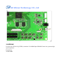
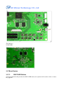
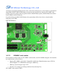
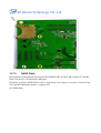
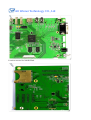
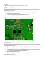
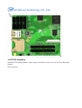
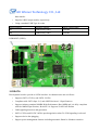
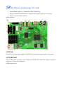
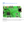
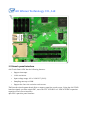
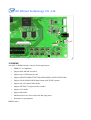
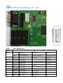
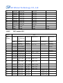
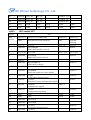
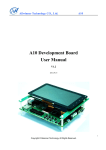
All Winner Technology CO., Ltd
A10 development board hardware manual
V1.1
August 24, 2011
All Winner Technology CO., Ltd
Version History
Version number
Date
Modifications
V1.0
2011-6-7
The initial version
V1.1
2011-8-24
According to EVB-V12, revise and improve
the
Remarks
All Winner Technology CO., Ltd
Table of contents
1A10 Development Board introduction...............................................................................................1
1.1A10 Overview.............................................................................................................................1
1.2Development Board Features......................................................................................................1
1.2.1Super video codec...............................................................................................................1
1.2.2Powerful audio capabilities.................................................................................................1
1.2.3Picture browsing.................................................................................................................1
1.2.4Features full e-book............................................................................................................1
1.2.5Large-capacity storage........................................................................................................1
1.2.6Super-rich peripheral interfaces .........................................................................................1
1.2.7A variety of start-up mode..................................................................................................1
1.2.8A variety of operating systems ...........................................................................................1
1.3Development board configuration..............................................................................................1
1.3.1Standard..............................................................................................................................1
1.3.2Optional ..............................................................................................................................1
1.4Functional block diagram of the development board.................................................................1
1.5Power tree diagram of the development board...........................................................................2
1.6Typical Applications...................................................................................................................2
1.7Documentation ...........................................................................................................................2
1.8Contact........................................................................................................................................2
1.9Chapter II hardware resources....................................................................................................2
1.10Dimensions diagram.................................................................................................................2
1.11Front picture..............................................................................................................................2
1.12Back picture..............................................................................................................................2
1.13Hardware resources...................................................................................................................2
1.14CPU ..........................................................................................................................................2
1.15Power supply.............................................................................................................................2
1.15.1Power input.......................................................................................................................2
1.15.2Power Output....................................................................................................................2
1.15.3PMU .................................................................................................................................2
1.15.4Power LED D2 .................................................................................................................2
1.15.5Charge status and alarm indicator D1 ..............................................................................2
1.15.6Reset button.......................................................................................................................2
1.15.7power soft-switching button .............................................................................................2
1.16DRAM .....................................................................................................................................2
1.17Boot Device .............................................................................................................................2
1.17.1RECOVER Button............................................................................................................2
1.17.2SD/MMC card socket .......................................................................................................2
1.17.3NAND Flash ....................................................................................................................2
1.18TF card socket ..........................................................................................................................2
1.19SDIO WIFI socket ...................................................................................................................2
1.20JTAG Interface.........................................................................................................................2
1.21Ethernet ....................................................................................................................................2
1.22EEPROM .................................................................................................................................2
1.23USB OTG ................................................................................................................................2
1.24USB HOST ..............................................................................................................................2
1.25SATA .......................................................................................................................................2
All Winner Technology CO., Ltd
1.26TV IN .......................................................................................................................................2
1.27CVBS OUT ..............................................................................................................................2
1.28VGA OUT ................................................................................................................................2
1.29TTL LCD .................................................................................................................................2
1.30LVDS LCD interfaces..............................................................................................................2
1.31touch panel interface.................................................................................................................2
1.32HDMI .......................................................................................................................................2
1.33Analog Audio Output................................................................................................................2
1.34Analog Audio Input..................................................................................................................2
1.35Microphone ..............................................................................................................................2
1.36User keys & LRADC................................................................................................................2
1.37Infrared Transceiver Interface..................................................................................................2
1.38UART .......................................................................................................................................2
1.39Camera sensor interfaces..........................................................................................................2
1.40Transport Stream Interface.......................................................................................................2
1.41TWI Interface (Two Wire Interface)........................................................................................2
1.42Gyro Interface...........................................................................................................................2
1.43G-Sensor Interface ...................................................................................................................2
1.44Light Sensor Interface ..............................................................................................................2
1.45 GPS Interface ..........................................................................................................................2
1.46Bluetooth Interface ..................................................................................................................2
1.47External Interrupt (EINT).........................................................................................................2
1.48signal defined expansion header...............................................................................................2
1.48.1IDC socket U11.................................................................................................................2
1.48.2IDC socket U12 ................................................................................................................2
1.48.3IDC socket U27 ................................................................................................................2
1.48.4IDC socket U29 ................................................................................................................2
1.48.5IDC socket U31 ................................................................................................................2
1 A10 Development Board introduction
1.1 A10 Overview
A10 uses ARM's Cortex-A8 processor, to build a whole new generation of intelligent network
processor SOC HD-A10, which will significantly enhance the level of SOC applications,
multimedia consumer electronics products and make the user experience has increased substantially
and improve the . A new generation of highly integrated processors will be the leading network
video performance and cost-effective features, widely used in tablet PCs, home intelligent HD
network players, automotive multimedia controller, network security monitoring, and a variety of
portable multimedia entertainment products and other emerging the market.
The A10, with technology to further promote the application of high-definition video codec
technology, SOC in the next-generation network integrates high-definition H.264 high Profile of
1080P coding techniques. Full high-definition format decoding technology will meet the multichannel decoding applications 1080P View.
The A10, with its own high-efficiency technology in the advanced graphics acceleration framework,
but also the introduction of ARM's MALI400 2D/3D graphics processor, to more smoothly support
the popular operating systems such as intelligent android2.3/3.0 for android product performance
and user experience will greatly enhance and improve.
All Winner Technology CO., Ltd
1.2 Development Board Features
A10 development board is designed specifically for the A10 chips, compact, full-featured, flexible.
Primarily for business for the A10, tablet PCs, home intelligent HD network players, automotive
multimedia controller, network security monitoring, and a variety of products such as portable
multimedia entertainment software and hardware development, debugging platform, or product
design information.
1.2.1 Super video codec
Support full HD (1920 * 1080P) video decoding, H.264, H.263, VC-1, MPEG-1/2/4, DIVX-3/4/5 /
6, XVID, WMV7 / 8, VP8, VP6 , AVS jizun, supports all major formats and other high-definition
video package almost all HD video formats; support for JPEG and H.264 encoding (1080P @
60fps; 720P @ 100fps)
Support H.264 encoding, 1080P @ 60fps, 720P @ 100fps.
1.2.2 Powerful audio capabilities
Music player supports all mainstream music, such as MP3, WMA, OGG, FLAC, APE, AAC,
ATRA, etc.
1.2.3 Picture browsing
Support high-definition JPEG, GIF, BMP formats. Maximum image size supported 16384x16384
(for 4:4:4 color formats)
1.2.4 Features full e-book
Support E-book, you can read epub, pdf, fb2, pdb, chm, html, txt and other format e-books; support
ANSI / ASCII, UTF-8, UTF16-BE, UTF16-LE, GB2312, EUC-KR, SHIFT -JIS, Windows1250/1251 other encoding formats; support English, Simplified Chinese, French, Italian, Spanish,
Dutch, Traditional Chinese, Japanese, Korean and other languages.
1.2.5 Large-capacity storage
256M 32 位 DDR2, 4G NAND memory, expandable to 8G (ECC 64, support for Samsung,
Toshiba, Hynix, Microm, Intel and other 5xnm, 4xnm, 3xnm, 2xnm process NAND);
1.2.6 Super-rich peripheral interfaces
USB2.0 OTG, USB2.0 HOST, HDMI1.3/1.4, LCD, CVBS-OUT, VGA-OUT, SATA, LINEIN、HEADPHONE、 10/100M Ethernet interface, 2 Camera Sensor Interfaces, SDIO WIFI,
GPS、 Gyroscope, Light Sensor, Bluetooth, Compass.
1.2.7 A variety of start-up mode
A variety of system startup, including NAND FLASH, SD / MMC card start-up; support USB for
flashing.
All Winner Technology CO., Ltd
1.2.8 A variety of operating systems
Support for the major operating systems, Android 2.3.4, Linux2.6, WinCE6.0.
1.3 Development board configuration
1.3.1 Standard
1. A10 development board
2. USB to serial debug line (USB switch to TTL)
3. 12V @ 2A power adapter
4. 5-inch LCD with touch screen module (TFT 800 * 480 high-definition, four-wire resistive
touch screen)
A10 Development
board
USB to serial debug Power adapter
cable
并口线
1.3.2 Optional
1. head board camera
2. SDIO WIFI module
3. 7-inch LCD with touch panel module (TFT 800 * 480 high-definition, TTL interface)
SDIO WIFI module
Camera head board
All Winner Technology CO., Ltd
1.4 Functional block diagram of the development board
All Winner Technology CO., Ltd
1.5 Power tree diagram of the development board
1.6 Typical Applications
•
•
•
Tablet PC
Smartphones
Smart TV
•
Video surveillance, traffic recorder, DV and other codec devices.
•
Smart Playlist box, sound bar, speakers and other home theater.
•
Games, advertising machines, industrial machines and other interactive devices.
All Winner Technology CO., Ltd
GPS, car entertainment systems.
•
1.7 Documentation
•
A10 Development Board Hardware User's Manual
•
A10 Android development board manual
•
A10 development board Linux Manual
•
A10 WinCE6.0 development board manual
•
A10 development board schematics.
•
A10 Datasheet
•
AXP209 Datasheet
1.8 Contact
Company: Zhuhai Zhi Technology Co., Ltd. all
Address: Zhuhai Southern Software Park Building, 4th Floor B6
Tel :0756 -3818315
Fax :0756 -3801678
All Winner Technology CO., Ltd
1.9 Chapter II hardware resources
1.10 Dimensions diagram
All Winner Technology CO., Ltd
1.11 Front picture
All Winner Technology CO., Ltd
1.12 Back picture
1.13 Hardware resources
Name
Description
CPU
Cortex-A8
32KB I-Cashe, 32KB D-Cache and 256KB L2 Cache
Trustzone Technology
PMU
X-Power AXP209 "flash charge core", 1.8A PWM switching charge,
intelligent power management controller, can receive 5V power adapter,
battery, USB5V power input, to provide 7 power outputs
DRAM
4 2Gbit 16 DDR3, total 1024MB DRAM.
NAND Flash
Hynix H27UBG8T2A, 4G Bytes MLC 64bit ECC NAND Flash, the board
can be expanded to two a total of 8G Bytes. Can be used as boot device.
TF Card Interface
Memory card can support up to 32G. Card detection
SD / MMC card
interface
Support SD / MMC card reader can be used as boot devices.
SDIO WIFI card
interface
For SDIO WIFI card
All Winner Technology CO., Ltd
Ethernet
10M/100M IEEE802.3, uses chip Realtek RTL8201CP
RJ45 connector
USB Host
2 USB Host interfaces, can support high-speed (HS, 480-Mbps),
full-speed (FS, 12-Mbps), and low-speed (LS, 1.5-Mbps)
data transmission
USB OTG
USB OTG 2.0. Host mode can support high-speed (480-Mbps),
full-speed (12-Mbps) and low-speed (1.5-Mbps) data transfer.
Device mode can support high-speed (480-Mbps), and full-speed
(12-Mbps) data transfer
TV-OUT Interface
CVBS (commonly known as AV) output
VGA-OUT Interface VGA output, maximum support 1920 * 1080 resolution
HDMI output
HDMI v1.3, up to 1080P @ 50/60fpts
LCD
Provides one 50pin FPC interface, one LCD screen interface as a 44pin IDC
Interface expansion
Development, can support a variety of screen sizes:
The following CPU 3-inch screen; 3-inch RGB display; 8 inch LVDS panel
TouchPanel
interface
Supports 4-wire resistive touch screen Interface capacitive touch screen and
TWI
Camera sensor
interface
Camera sensor offers two sets of interface signals. NTSC and PAL
CCIR656
Protocol support 8-bit input data
Microphone
Supports 2-way MIC input
Headphone
Stereo headphone output.
Line-in
2 audio inputs.
TWI
Development board provides two sets of TWI interfaces
UART
Provides one UART interface: TTL level or RS232 level.
JTAG
JTAG debug interface.
Buttons
Provides five definable function keys and RESET and POWER_ON keys.
Infrared data
reception
IR supports only infrared data reception.
Battery Interface
Such as single-cell 4.1V/4.15V/4.2V/4.36V lithium battery, rechargeable.
AC adapter
connector
12V DC power supply.
The third chapter details the hardware
This section will describe in detail the various hardware development board A10 module, interface,
technical parameters, pin definitions, related configuration, use precautions.
All Winner Technology CO., Ltd
1.14 CPU
The A10 CPU is a cost effective, high integration, high performance, low-power 16/32-bit
multimedia applications processor. The CPU core is a Cortex-A8 with 32KB instruction, 32KB
data and 256K L2 caches. The CPU integrates many features to reduce overall system cost and
product development effort. Using 441 pin 0.8mm pitch BGA package. Small size, low power, low
heat.
1.15 Power supply
1.15.1
Power input
Tha A10 board can use any compination of the 12V power adapter, battery os USB power. The
PMU will do the smart choice to determine:
1. 12V power adapter, input from the J1 connector, provides up to 2A current. 12V DC power
supply through one DCDC chip MP1482D, output 5V @ 2A for the PMU to use, but also
for the two USB HOST Interface: USB1, USB2.
2. Battery-powered, input from the J2 connector. Such as single-cell support
4.1V/4.15V/4.2V/4.36V lithium batteries (lithium ion or lithium polymer). The default
target battery voltage (Vtrgt) 4.2V, Automatic recharge voltage (Vtrgt-0.1) V. Vtrgt set by
PMU registers.
3. USB power input, the input from a P2 USB OTG Interface 5V power supply.
USB power socket
Battery socket
All Winner Technology CO., Ltd
12V power connector
12V power switch
1.15.2
Power Output
From the J12 socket output DC 12V, DC 5V, DC 3.3V, GND. For user extensions.
Power outlet
All Winner Technology CO., Ltd
1.15.3
PMU
PMU choices are highly integrated power system management chip AXP209, which integrates an
adaptive PWM charger's USB-Compatible, 2 step-down converter (Buck DC-DC Converter), 5
linear regulators (LDO ), voltage / current / temperature multi-channel 12-Bit ADC, and 4-way
configurable GPIO. In order to ensure power system security and stability, AXP209 also
incorporates over / under voltage (OVP / UVP), over temperature (OTP), overcurrent (OCP) and
other protective circuits.
AXP209 provides a two-wire serial communication interface: Two Wire Interface (TWI), the
application processor can use this interface to turn on or off certain power output, the voltage set
them to access the internal registers and a variety of measurement data (including Fuel Gauge).
High accuracy (1%, mainly by the 1% precision resistors BIAS decision) to facilitate measurement
of electricity consumers to grasp more clearly the real-time energy usage.
AXP209 intelligent energy balance (Intelligent Power Select, IPSTM) circuit in the USB, and
external AC adapter, battery and load application transparent distribution of power between the
safety and the only external input power without the battery (or battery discharge / damage) in the
case also allows applications to work properly. The specific energy distribution as follows:
•
When the only access to lithium batteries, no external power input (VBUS or ACIN), the
use of lithium-powered;
•
When an external supply (VBUS or ACIN), preferred to use an external power supply;
•
The case of the battery connection, external power supply is removed, immediately
"seamless" switches to battery power supply;
All Winner Technology CO., Ltd
•
When VBUS and ACIN both access, the priority ACIN power, and to charge the lithium
battery;
•
If not enough ACIN drive capability, it will open the VBUS timely access, to achieve
ACIN / VBUS common power supply;
•
If the drive capacity is still insufficient, it will reduce the charge current up to 0, then added
with the battery power supply;
AXP209
1.15.4
Power LED D2
PMU works, the power light is light D2; otherwise off the power indicator D2.
Power LED D2
All Winner Technology CO., Ltd
1.15.5
Charge status and alarm indicator D1
D1 indicates charging status indicator and alarm, which indicates that four states: charging, not
charging, battery and external power supply abnormal overvoltage alarm alarm. As follows:
LED status
Note
Steady
Charging
Off
Not charging
Flashes at 1Hz
Battery usage or the charge level into the battery is too low
Flashes at 4Hz frequency
PMU input voltage is too high
Charge status and alarm indicator
All Winner Technology CO., Ltd
1.15.6
Reset button
Development board provides a reset button, the development board can be reset.
Reset button
All Winner Technology CO., Ltd
1.15.7
power soft-switching button
Development board provides a soft power switch button, connected to the PMU POWON signal.
By default, press (6 seconds) to achieve the power output of all PMU (RTC power LDO1 excluded)
of the switch.
PMU can identify this button "press" and "Press" and send to the CPU IRQ, so users can customize
the "long press" and "press" the button application. Specifically refer to the AXP209 Datesheet.
Soft power switch button
All Winner Technology CO., Ltd
1.16 DRAM
Use the four 2G Bit 16 位 DDR3, constitute 32 1024M Bytes DRAM. Ensure the system's highspeed operation.
Frontal two
2GBit DDR3
All Winner Technology CO., Ltd
The back two
2GBit DDR3
1.17 Boot Device
1.17.1
RECOVER Button
A10 development board provides the RECOVER button, the system can be used to select or start a
key upgrade.
All Winner Technology CO., Ltd
A10 and it can support multiple device boot, when the system power or reset button is pressed first
check RECOVER, if RECOVER button not pressed, the system first from the SD / MMC card
(U26) to boot the system, failed to guide from the NAND Flash system, NAND Flash boot failure
from USB0 download firmware.
If you hold down the RECOVER button, the system skips all the boot device, download the
firmware from USB0.
RECOVER Button
1.17.2
SD/MMC card socket
Development board provides an SD / MMC card interface, the SD CARD0 using the A10 interface.
Its characteristics are as follows:
•
Support SD / MMC card reader. Compatible with Secure Digital memory (up to SD3.0),
Secure Digital I / O, Multimedia Card (up to MMC4.3).
•
Memory card can support up to 32G.
•
Provide 3.3V voltage, providing card detection (interrupt IO).
SD / MMC card socket (Card0)
All Winner Technology CO., Ltd
1.17.3
NAND Flash
Development board equipped with a Hynix H27UBG8T2ATB, 4G Bytes MLC 64bit ECC NAND
Flash. Use the four CE signal and 2 RB signal.
Board also set aside a NAND Flash location. Supports up to two single or two pairs of selected chip
select NAND. Maximum capacity to support 16G.
4G NAND Flash
All Winner Technology CO., Ltd
Location reserved for NAND Flash
All Winner Technology CO., Ltd
1.18 TF card socket
Development board provides an interface to TF card, the SD CARD1 using the A10 interface. Its
characteristics are as follows:
•
Support TF card reader, compatible with Secure Digital memory (up to SD3.0).
•
Memory card can support up to 32G.
•
Provide 3.3V voltage, providing card detection (interrupt IO).
TF card socket (Card1)
1.19 SDIO WIFI socket
Development board provides an SDIO WIFI card interface, the SD CARD3 using the A10 interface.
Its characteristics are as follows:
•
Developed primarily for SDIO WIFI card use. Support SDIO 1-bit and 4-bit interrupt mode;
support suspend and resume operation; support read wait.
•
Also available for SD / MMC card. Compatible with Secure Digital memory (up to SD3.0),
Secure Digital I / O, Multimedia Card (up to MMC4.3).
•
Memory card can support up to 32G.
•
Provide 3.3V voltage, providing card detection (interrupt IO).
SDIO WIFI socket (Card3)
All Winner Technology CO., Ltd
1.20 JTAG Interface
Standard JTAG debug interface offers 14pin 2.0mm IDC socket. User via the JTAG debug the
system.
JTAG Interface
All Winner Technology CO., Ltd
1.21 Ethernet
evelopment board provides network functionality, network interface chip REALTEK RTL8201CP
chip. Its characteristics are as follows:
•
Interface uses a Link / Active LED and isolation transformer RJ45 socket.
•
Compatible with IEEE802.3 standards, support full and half duplex operation.
•
Support 10/100M data rate.
Network interface chip
Ethernet RJ45 socket
All Winner Technology CO., Ltd
1.22 EEPROM
Onboard a 2 Mbytes EEPROM AT24C16B, using the system TWI1 interface communication.
MAC address can be used as storage or other applications.
2M Bytes EEPROM
1.23 USB OTG
Development board provides a USB OTG interface, use the A10 USB0 interface. Its characteristics
All Winner Technology CO., Ltd
are as follows:
•
Fully compatible with USB OTG 2.0 specification.
•
Can be configured as stand-alone USB HOST or USB DEVICE, fully compatible with USB
2.0 specification.
•
Host mode can support high-speed (480-Mbps), full-speed (12-Mbps) and low-speed (1.5Mbps) data transfer.
•
Device mode can support high-speed (480-Mbps) and full-speed (12-Mbps) data transfer.
•
Can detect VBUS insert, ID signal.
•
Can enable the VBUS output, VBUS output current limiting 1A.
•
Using a standard MINI-USB socket.
Socket number Interface signals
VBUS output enable
P2
DM0/DP0(USB0) GPIOB9
USB OTG (USB0)
VBUS detection
ID detection
GPIOH5
GPIOH4
1.24 USB HOST
Development board provides two USB HOST interfaces, respectively, using the A10 interface to
the USB1 and USB2 interface. Its characteristics are as follows:
•
Fully compatible with USB 2.0 specification.
•
Able to support high-speed (480-Mbps), full-speed (12-Mbps) and low-speed (1.5-Mbps)
All Winner Technology CO., Ltd
data transfer.
•
Supplies VBUS output enable, respectively.
•
Using a standard USB Type A socket.
Socket number
Interface signals
VBUS output enable
P3
DM1/DP1(USB1)
GPIOH6
P4
USB HOST (USB1)
DM2/DP2(USB2)
GPIOH3
USB HOST (USB2)
1.25 SATA
Development board to provide a SATA interface. Its characteristics are as follows:
•
Supports SATA 1.5Gb/s, and SATA 3.0Gb/s
•
Compliant with SATA Spec. 2.6, and AHCI Revision 1.3 Specifications
•
Supports industry-standard AMBA High-Performance Bus (AHB) and it is fully compliant
with the AMBA Specification, Revision 2.0. Supports 32-bit Little Endian
•
OOB signaling detection and generation
•
SATA 1.5Gb/s and SATA 3.0Gb/s speed negotiation when Tx OON signaling is selected
•
Supports device hot-plugging
•
Support power management features including automatic Partial to Slumber transition
All Winner Technology CO., Ltd
•
Internal DMA Engine for Command and Data Transactions
•
Supports hardware-assisted Native Command Queuing (NCQ) for up to 32-entries
•
Support external SATA (eSATA)
SATA connector
1.26 TV IN
Provides 3-way video input, support CCIR-656 4:2:2 8-bit parallel input format. Using Cinch.
1.27 CVBS OUT
Video CVBS output to provide a way to support 4 X12-bit DAC output data. Using Lotus jack for
connecting TV and other equipment.
CVBS output socket
All Winner Technology CO., Ltd
1.28 VGA OUT
VGA output support RGB. Support for 4 X12-bit DAC output data. Using DB15 socket, can be
directly output to the computer monitor. Easy to use monitor for video development.
VGA output socket
All Winner Technology CO., Ltd
1.29 TTL LCD
A10 LCD controller has the following features:
•
Support the HV-DE-Sync (digital parallel RGB) input LCD panels (Max 1024 * 1024
resolution ,24-bit color).
•
Support the HV-DE-Sync (digital serial RGB, both delta and stripe panel) input LCD panels
(Max 680 * 1024 resolution, up to true color).
•
Support TTL (digital RGB) input LCD panels (Max 1024 * 1024 resolution, 18-bit color).
•
Support Analog RGB input LCD panels (Max 1024 * 1024 resolution, 3 channel 6bit DAC
output).
•
Support 18/16/9/8bit 8080 CPU I / F panels (Max 1024 * 1024 resolution).
•
CCIR-656 output interface.
Onboard a 50pin FPC socket and plugs directly into supporting the 5-inch 800 * 480 high-definition
LCD touch screen, or other TTL LCD support for development.
While providing a 44pin 2.0mm IDC expansion socket outlet as the LCD for users to develop other
dimensions of LCD applications. Provide three GPIO Using as LCD control, a PWM as the
backlight control. 3.3V and 5V power output. 3.3V power supply controlled by the GPIO off.
50pin LCD FPC
44pin 2.0mm LCD
All Winner Technology CO., Ltd
1.30 LVDS LCD interfaces
Provides four LVDS outputs: 3 sets of data signals and a set of clock signals.
Provide three GPIO as LCD control, a PWM as backlight control.
3.3V and 5V power output. 3.3V power supply controlled by the GPIO off.
Provide four-wire resistive touch screen interface signals.
Using a 44pin 2.0mm IDC connector. Can insert the optional LVDS LCD module development.
Note:
•
FPC connector J9, IDC sockets U7, IDC socket U8 multiplexing a signal, at the same time
can only use one interface.
•
VGA and TTL LCD common signal HSYNC and VSYNC, VGA and TTL LCD can not be
used.
44pin 2.0mm LVDS LCD IDC
All Winner Technology CO., Ltd
1.31 touch panel interface
A10 Touch Panel ADC has the following features:
•
Support interrupts.
•
11-bit resolution.
•
Input voltage range: 0V to 2/3AVCC (2.0V).
•
Sampling rates up to 128K.
•
Support the four-wire resistive touch screen.
TWI interface development board Able to support capacitive touch screen, Using the A10 TWI2
interface signals. provides a 4pin FPC, users can TTL LCD IDC or LVDS LCD IDC expansion
capacitive touch screen interface.
4pin FPC capacitive panel interface
All Winner Technology CO., Ltd
1.32 HDMI
A10 built-in HDMI interface, has the following features:
•
HDMI V1.3 compliance
•
Support Max 4K*4K resolution
•
Support up to 165M pixel/second
•
Support 480I/576I/480P/576P/720P/1080I/1080P at 24/25/30/50/50.9Hz
•
Support 24/30/36/48-bit RGB data format,with 2X/4X repeater
•
Support up to 8 channel,24bit PCM
•
Support IEC61937 compress audio formats
•
Support 1-bit audio
•
Support HD audio
•
Hardware Receiver active sense and Hot plug detect
•
Interrupts for programmer
HDMI socket
All Winner Technology CO., Ltd
1.33 Analog Audio Output
Development board provides two analog audio output with 3.5mm stereo headphone jack. Using
DC coupling.
Audio output jack
All Winner Technology CO., Ltd
1.34 Analog Audio Input
Development board provides two analog audio inputs, 3.5mm stereo headphone jack.
AC coupling.
24-bit DAC。
Support for 48K and 44.1K sampling rate
Support for 192K and 92K sampling.
Audio input jack
All Winner Technology CO., Ltd
1.35 Microphone
Onboard two-way Microphone, stereo recording can be done the development.
24-bit DAC。
Support for 48K and 44.1K sampling rate
Support for 192K and 92K sampling.
Left Mic
All Winner Technology CO., Ltd
Right Mic
All Winner Technology CO., Ltd
1.36 User keys & LRADC
A10 provides a two-way Low Resolution ADC input (LRADC0, LRADC1), as a key application.
Its characteristics are as follows:
•
Support interrupts.
•
6-bit resolution.
•
Voltage input range 0 to 0.67 * AVCC (AVCC is LRADC reference voltage).
•
Sampling rates up to 250HZ.
LRADC0 is connected to the development board, predefined commonly used for the ANDRIOD's
seven buttons: VOL +, VOL-, MENU, SEARCH, HOME, ESC, ENTER. Users can also customize
the button functions.
A10 also provides RECOVER button can be used as a key boot options or upgrades. See Boot
Device.
LRADC1 for user extensions. IDC socket for the user in the form of expansion and development to
define the signal socket see "expansion connector signal definitions."
1.37 Infrared Transceiver Interface
A10 were provided along the way IR-RX and IR-TX. Its characteristics are as follows:
•
Compatible with MIR FIR IrDA 1.1.
•
Supports 0.576 Mbit / s and 1.152 Mbit / s Medium Infrared (MIR).
•
Supports 4 Mbit / s FIR IrDA 1.4.
All Winner Technology CO., Ltd
•
Support CIR remote control or wireless keyboard.
IR-RX is connected to the onboard infrared receiver, remote control receiver can be applied directly
to do.
IR-TX for user extensions. IDC socket to form for users to expand the development, definition of
socket signals see "expansion socket signal definition"。
Infrared receiver
1.38 UART
Development board provides one UART interface: UART0.
Is the standard UART0 RX, TX two-wire serial interface, debug printing as the default interface,
the default baud rate is 115200. UART0 supports TTL-level output can be connected to serial port
supporting USB (TTL) lines, such as user-friendly notebook PC without RS232 port for debugging
print. UART0 also supports RS232 level output. RS232 level output port Using DB9 female socket.
RS232 DB9 UART0
TTL UART0
All Winner Technology CO., Ltd
1.39 Camera sensor interfaces
Camera sensor development board provides two sets of interface signals. Its characteristics are as
follows:
•
NTSC and PAL CCIR656 agreement.
•
Supports 8-bit input data.
•
TWI signal and provides a set of two GPIO signals for controlling the camera to use.
•
Provides 2.8V and 5V power supply.
IDC socket to form for users to expand the development, definition of socket signals see "expansion
socket signal definitions."
1.40 Transport Stream Interface
A10 Transport Stream controller has the following features:
•
One external Synchronous Parallel Interface (SPI) or one external Synchronous Serial
Interface (SSI)。
•
32 channels PID filter
•
Multiple transport stream packet (188, 192, 204) format support
•
SPI and SSI timing parameters are configurable
•
Hardware packet synchronous byte error detecting
All Winner Technology CO., Ltd
•
Hardware PCR packet detecting
•
Configurable SPI transport stream generator for streams in DRAM memory
•
DMA is supported for transferring data
•
Interrupt is supported
•
Support DVB-CSA V1.1 Descrambler
Development board offers two TS signal for the Mobile TV use.
IDC socket to form for users to expand the development, definition of socket signals see "expansion
socket signal definitions."
1.41 TWI Interface (Two Wire Interface)
A10 TWI interface has the following characteristics:
•
Software-programmable for Slave or Master
•
Supports Repeated START signal
•
Multi-master systems supported
•
Allows 10-bit addressing with 2-Wire bus
•
Performs arbitration and clock synchronization
•
Own address and General Call address detection
•
Interrupt on address detection
•
Supports speeds up to 400Kbits/s (‘fast mode’)
•
Allows operation from a wide range of input clock frequencies
Development board provides two interfaces for users to extend the use of TWI.
IDC socket to form for users to expand the development, definition of socket signals see "expansion
socket signal definitions."
1.42 Gyro Interface
IDC socket to form for users to expand the development, definition of socket signals see "expansion
socket signal definitions."
1.43 G-Sensor Interface
IDC socket to form for users to expand the development, definition of socket signals see "expansion
socket signal definitions."
1.44 Light Sensor Interface
IDC socket to form for users to expand the development, definition of socket signals see "expansion
socket signal definitions."
All Winner Technology CO., Ltd
1.45 GPS Interface
IDC socket to form for users to expand the development, definition of socket signals see "expansion
socket signal definitions."
1.46 Bluetooth Interface
IDC socket to form for users to expand the development, definition of socket signals see "expansion
socket signal definitions."
1.47 External Interrupt (EINT)
A10 provides up to 32 external interrupts. Development board will be one of the 20 external
interrupts to IDC socket for the user to extend the form of development, definition of socket signals
see "expansion connector signal definitions."
1.48 signal defined expansion header
Development board provides five 2.0mm IDC-20 socket for expansion capabilities. Users can use
our complementary capabilities to extend sub-board functional development, or design their own
sub-board for extensions development. This section will describe the form of a list of the PIN of the
expansion header pin signal definitions and functions.
Caution is as follows:
•
The same PIN can only be used at the same time the same function.
•
Recommend using the recommended function, there will be a better software support, thus
reducing development effort and workload.
•
The default state is GPIO GPIO input, if used for output, then the external pull-up resistor
on the circuit or a pull-down resistor. Required to determine the polarity of the signal is to
spend or pull-down resistors.
All Winner Technology CO., Ltd
1.48.1
IDC socket U11
Socket
PIN
number
U11
Function 1
Function 2
(recommended)
Function 3
Function 4
GPIO
Camera Sensor 0
Transport Stream 0
External interrupt
1
VCC-5V
VCC-5V
VCC-5V
VCC-5V
2
GPIOH16
CSI0-PWR
3
EINT16
CSI-IO-2.8V
4
GPIOH13
CSI0-RST#
EINT13
5
GPIOE0
CSI0-PCK
6
GPIOB18
TWI1-SCK
7
GPIOB19
TWI1-SDA
8
GPIOE3
CSI0_VSYNC
TS0_DVLD
9
GPIOE2
CSI0_HSYNC
TS0_SYNC
10
GPIOE1
CSI0_CK
TS0_ERR
TS0-CLK
All Winner Technology CO., Ltd
11
GPIOE4
CSI0_D0
TS0_D0
12
GPIOE5
CSI0_D1
TS0_D1
13
GPIOE6
CSI0_D2
TS0_D2
14
GPIOE7
CSI0_D3
TS0_D3
15
GPIOE8
CSI0_D4
TS0_D4
16
GPIOE9
CSI0_D5
TS0_D5
17
GPIOE10
CSI0_D6
TS0_D6
18
GPIOE11
CSI0_D7
TS0_D7
19
GND
GND
GND
GND
20
GND
GND
GND
GND
1.48.2
IDC socket U12
Socket
PIN
number
U12
Function
1
Function 2 Function 3 Function 4
(recommend
ed)
Function 5
Function 6
GPIO
Camera
Sensor 1
Transport
Stream 1
SD Card 1
UART3/4
External
interrupt
1
VCC-5V VCC-5V
VCC-5V
VCC-5V
VCC-5V
VCC-5V
2
GPIOH17 CSI1-PWR
3
EINT17
CSI-IO-2.8V
4
GPIOH14 CSI1-RST#
5
GPIOG0
6
GPIOB18 TWI1-SCK
7
GPIOB19 TWI1-SDA
8
GPIOG3
9
CSI1-PCK
EINT14
TS1-CLK
SDC1_CMD
CSI1_VSY
NC
TS1_DVL
D
SDC1_D1
GPIOG2
CSI1_HSY
NC
TS1_SYN
C
SDC1_D0
10
GPIOG1
CSI1_CK
TS1_ERR
SDC1_CLK
11
GPIOG4
CSI1_D0
TS1_D0
SDC1_D2
12
GPIOG5
CSI1_D1
TS1_D1
SDC1_D3
13
GPIOG6
CSI1_D2
TS1_D2
UART3_TX
14
GPIOG7
CSI1_D3
TS1_D3
UART3_RX
15
GPIOG8
CSI1_D4
TS1_D4
UART3_RTS
All Winner Technology CO., Ltd
16
GPIOG9
CSI1_D5
TS1_D5
UART3_CTS
17
GPIOG10 CSI1_D6
TS1_D6
UART4_TX
18
GPIOG11 CSI1_D7
TS1_D7
UART4_RX
19
GND
GND
GND
GND
GND
GND
20
GND
GND
GND
GND
GND
GND
1.48.3
IDC socket U27
Socket
U27
PIN
number
Function 1 Function 2 (recommended)
Function 3
Function 4
GPIO
WIFI/PA/LS/GS/CP/TWI1/GY
IR0
External
interrupt
1
VCC-5V
VCC-5V
VCC-5V
VCC-5V
2
GPIOH9
WIFI-SHDN#
(SDIO WIFI standby control)
3
VCC-3.3V VCC-3.3V
4
GPIOH12
5
GPIOI3
6
EINT9
VCC-3.3V
VCC-3.3V
WIFI-PWR
(SDIO WIFI power control)
EINT12
GPIOH10
WIFI-WAKEUP
(SDIO WIFI wakeup)
EINT10
8
GPIOH15
PA-SHDN#
(Audio PA shutdown control signal)
EINT15
9
GPIOH20
LS-INT
(Light sensor interrupt input)
EINT20
10
GPIOH0
GS-INT1
(External G-sensor interrupt input signal)
EINT0
11
GPIOB3
CP-RST#
(Compass reset signal)
12
GPIOI13
CP-INT
(Compass interrupt input)
13
GND
GND
GND
GND
14
GND
GND
GND
GND
15
GPIOB18
TWI1-SCK
16
GPIOB19
TWI1-SDA
17
GPIOH18
GY-INT1
(Gyroscope interrupt input)
EINT18
18
GPIOH19
GY-INT2
EINT19
7
IR0-TX
EITN25
All Winner Technology CO., Ltd
(Gyroscope interrupt input)
19
GND
GND
GND
GND
20
GND
GND
GND
GND
1.48.4
IDC socket U29
Socket
U29
PIN
number
Function 1
Function 2 (recommended)
Function 3 Function 4
GPIO
GPS/TWI1/LRADC1/TP
PS2-1
External interrupt
1
VCC-5V
VCC-5V
VCC-5V
VCC-5V
2
GPIOI0
GPS-CLK
(GPS clock signal)
3
VCC-3.3V
VCC-3.3V
4
GPIOI1
GPS-SIGN
(GPS data0)
5
GPIOI14
GPS-OSC-EN
(GPS clock control)
6
GPIOI2
GPS-MAG
(GPS data1)
7
GPIOC22
GPS-VCC-EN
(GPS power control)
8
GPIOC19
GPS-SCS
(GPS SPI chip select)
9
GPIOI15
GPS-RX-EN
(GPS RX enable)
10
GPIOC20
GPS-SCLK
(GPS SPI serial clock)
11
VCC-3.3V VCC-3.3V
PS2-SCK1 EINT26
PS2-SDA1 EINT27
LRADC1
(Low Resolution ADC input)
12
GPIOC21
GPS-MOSI
(GPS SPI data output)
13
GND
GND
GND
GND
14
GND
GND
GND
GND
15
GPIOB20
TWI2-SCK
16
GPIOB21
TWI2-SDA
17
GPIOH21
TP-INT
(External TP interrupt input)
18
GPIOB13
TP-WAKEUP
(External TP wake up)
EINT21
All Winner Technology CO., Ltd
19
GND
GND
GND
GND
20
GND
GND
GND
GND
1.48.5
IDC socket U31
Socket
PIN
number
U31
Function 1
Function 2
(recommended)
Function 3
Function 4
Function 5
GPIO
Bluetooth
UART2
PS2-0
External
interrupt
1
VCC-5V
VCC-5V
VCC-5V
VCC-5V
VCC-5V
2
GPIOB5
BT-RST#
(Bluetooth reset)
3
VCC-3.3V
VCC-3.3V
VCC-3.3V
VCC-3.3V
VCC-3.3V
4
GPIOB6
BT-PCM-CLK
(Bluetooth PCM
clock signal)
5
GPIOB12
BT-PCM-IN
(Bluetooth PCM
data input)
6
GPIOB7
BT-PCM-SYNC
(Bluetooth PCM
sync)
7
GPIOI16
BT-UART-RTS
(Bluetooth UART
RTS)
8
GPIOB8
BT-PCM-OUT
(Bluetooth PCM
data out)
9
GPIOI18
10
UART2-RTS
EINT28
BT-UART-TX
(Bluetooth UART
TX)
UART2-TX
EINT30
GPIOI17
BT-UART-CTS
(Bluetooth UART
CTS)
UART2-CTS
EINT29
11
GPIOI20
BT-GPIO0
(Bluetooth GPIO)
12
GPIOI19
BT-UART-RX
(Bluetooth UART
RX)
UART2-RX
13
GND
GND
GND
PS2-SCK0
EINT31
GND
GND
All Winner Technology CO., Ltd
14
GND
GND
GND
GND
GND
15
GPIOI21
BT-GPIO1
(Bluetooth GPIO)
16
GPIOI12
17
GPIOI10
18
GPIOI11
19
GND
GND
GND
GND
GND
20
GND
GND
GND
GND
GND
PS2-SDA0
GS-INT2