1
RM0308
Reference manual
SPEAr320 address map and registers
Introduction
This document provides the address map and register descriptions for the SPEAr320,
embedded MPU with ARM926 core. Additional reference information is documented in the
manual RM0307: SPEAr320 architecture and functionality.
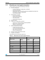
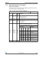
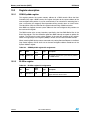
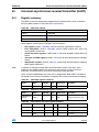
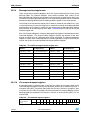
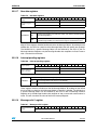
IP groups
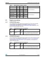
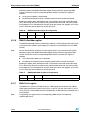
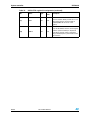
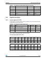
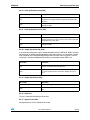
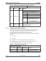
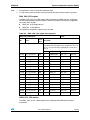
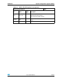
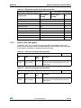
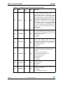
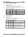
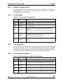
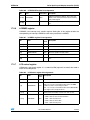
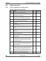
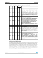
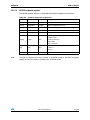
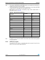
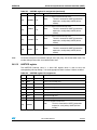
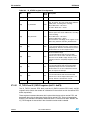
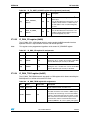
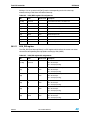
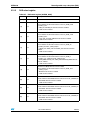
Table 1.
SPEAr320 IP groups
IP group
Constituent IPs
Processors, &
busses
ARM926EJ-S
Bus interconnection matrix
Vectored interrupt controller (VIC)
General device
resources
Direct memory access controller (DMAC)
General purpose timers (GPT)
Real-time clock (RTC)
System controller
Watchdog timer
Security co-processor (C3)
System configuration registers (MISC)
Memory
interfaces
DDR multiport controller (MPMC)
Memory card interface (MCIF)
Serial memory interface (SMI)
Flexible static memory controller (FSMC)
Extended memory interface (EMI)
Graphics, video,
& audio
Color liquid crystal display controller (CLCD)
JPEG codec
High-speed
connectivity
Media independent interface (MII)
Serial Media Independent Interface (SMII)
USB2.0 Host
USB 2.0 Device
September 2011
Doc ID 022180 Rev 1
1/533
www.st.com
SPEAr320
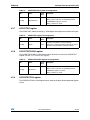
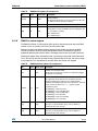
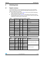
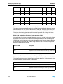
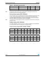
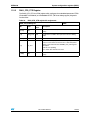
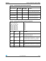
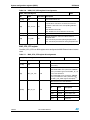
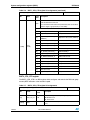
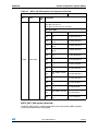
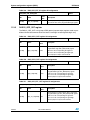
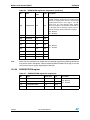
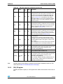
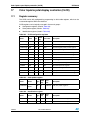
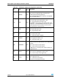
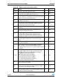
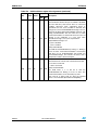
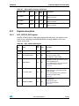
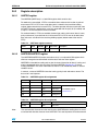
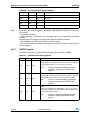
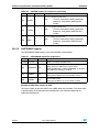
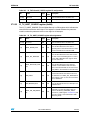
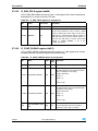
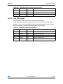
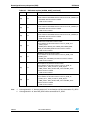
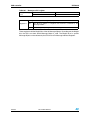
Table 1.
IP group
Other
connectivity
2/533
SPEAr320 IP groups (continued)
Constituent IPs
Analog-to-digital convertor (ADC)
Universal asynchronous receiver/transmitter (UART)
Extended general purpose I/O (XGPIO)
General purpose I/Os (GPIO)
I2C controller
Pulse Width Modulator (PWM)
Standard parallel port interface (SPP)
Fast IrDA controller
Reconfigurable array subsystem (RAS)
CAN controller
Synchronous serial ports (SSP)
Touchscreen block
Doc ID 022180 Rev 1
SPEAr320
Contents
Contents
1
Address map . . . . . . . . . . . . . . . . . . . . . . . . . . . . . . . . . . . . . . . . . . . . . . 22
2
ARM926EJ-S . . . . . . . . . . . . . . . . . . . . . . . . . . . . . . . . . . . . . . . . . . . . . . 25
3
Bus interconnection matrix . . . . . . . . . . . . . . . . . . . . . . . . . . . . . . . . . . 26
4
Vectored interrupt controller (VIC) . . . . . . . . . . . . . . . . . . . . . . . . . . . . 27
5
4.1
Register summary . . . . . . . . . . . . . . . . . . . . . . . . . . . . . . . . . . . . . . . . . . 27
4.2
Register descriptions . . . . . . . . . . . . . . . . . . . . . . . . . . . . . . . . . . . . . . . . 29
4.2.1
VICIRQSTATUS register . . . . . . . . . . . . . . . . . . . . . . . . . . . . . . . . . . . . 29
4.2.2
VICFIQSTATUS register . . . . . . . . . . . . . . . . . . . . . . . . . . . . . . . . . . . . 29
4.2.3
VICRAWINTR register . . . . . . . . . . . . . . . . . . . . . . . . . . . . . . . . . . . . . . 30
4.2.4
VICINTSELECT register . . . . . . . . . . . . . . . . . . . . . . . . . . . . . . . . . . . . 30
4.2.5
VICINTENABLE register . . . . . . . . . . . . . . . . . . . . . . . . . . . . . . . . . . . . 30
4.2.6
VICINTENCLEAR register . . . . . . . . . . . . . . . . . . . . . . . . . . . . . . . . . . . 30
4.2.7
VICSOFTINT register . . . . . . . . . . . . . . . . . . . . . . . . . . . . . . . . . . . . . . 31
4.2.8
VICSOFTINTCLEAR register . . . . . . . . . . . . . . . . . . . . . . . . . . . . . . . . 31
4.2.9
VICPROTECTION register . . . . . . . . . . . . . . . . . . . . . . . . . . . . . . . . . . 31
4.2.10
VICVECTADDR register . . . . . . . . . . . . . . . . . . . . . . . . . . . . . . . . . . . . 32
4.2.11
VICDEFVECTADDR register . . . . . . . . . . . . . . . . . . . . . . . . . . . . . . . . . 32
4.2.12
VICVECTADDR register . . . . . . . . . . . . . . . . . . . . . . . . . . . . . . . . . . . . 32
4.2.13
VICVECTCNTL register . . . . . . . . . . . . . . . . . . . . . . . . . . . . . . . . . . . . . 33
4.2.14
Peripheral identification registers . . . . . . . . . . . . . . . . . . . . . . . . . . . . . . 33
4.2.15
VICPERIPHID0 register . . . . . . . . . . . . . . . . . . . . . . . . . . . . . . . . . . . . . 33
4.2.16
VICPERIPHID1 register . . . . . . . . . . . . . . . . . . . . . . . . . . . . . . . . . . . . . 34
4.2.17
VICPERIPHID2 register . . . . . . . . . . . . . . . . . . . . . . . . . . . . . . . . . . . . . 34
4.2.18
VICPERIPHID3 register . . . . . . . . . . . . . . . . . . . . . . . . . . . . . . . . . . . . . 34
4.2.19
Identification registers . . . . . . . . . . . . . . . . . . . . . . . . . . . . . . . . . . . . . . 35
4.2.20
VICPCELLID0 register . . . . . . . . . . . . . . . . . . . . . . . . . . . . . . . . . . . . . . 35
4.2.21
VICPCELLID1 register . . . . . . . . . . . . . . . . . . . . . . . . . . . . . . . . . . . . . . 35
4.2.22
VICPCELLID2 register . . . . . . . . . . . . . . . . . . . . . . . . . . . . . . . . . . . . . . 35
4.2.23
VICPCELLID3 register . . . . . . . . . . . . . . . . . . . . . . . . . . . . . . . . . . . . . . 35
Direct memory access controller (DMAC) . . . . . . . . . . . . . . . . . . . . . . . 37
Doc ID 022180 Rev 1
3/533
Contents
6
7
4/533
SPEAr320
5.1
Register summary . . . . . . . . . . . . . . . . . . . . . . . . . . . . . . . . . . . . . . . . . . 37
5.2
Register description . . . . . . . . . . . . . . . . . . . . . . . . . . . . . . . . . . . . . . . . . 38
5.2.1
DMACIntStatus register . . . . . . . . . . . . . . . . . . . . . . . . . . . . . . . . . . . . . 38
5.2.2
DMACIntTCStatus register . . . . . . . . . . . . . . . . . . . . . . . . . . . . . . . . . . 38
5.2.3
DMACIntTCClear register . . . . . . . . . . . . . . . . . . . . . . . . . . . . . . . . . . . 39
5.2.4
DMACIntErrorStatus register . . . . . . . . . . . . . . . . . . . . . . . . . . . . . . . . . 39
5.2.5
DMACIntErrClr register . . . . . . . . . . . . . . . . . . . . . . . . . . . . . . . . . . . . . 39
5.2.6
DMACRawIntTCStatus register . . . . . . . . . . . . . . . . . . . . . . . . . . . . . . . 40
5.2.7
DMACRawIntErrorStatus register . . . . . . . . . . . . . . . . . . . . . . . . . . . . . 40
5.2.8
DMACEnbldChns register . . . . . . . . . . . . . . . . . . . . . . . . . . . . . . . . . . . 40
5.2.9
DMACSoftBReq register . . . . . . . . . . . . . . . . . . . . . . . . . . . . . . . . . . . . 41
5.2.10
DMACSoftSReq register . . . . . . . . . . . . . . . . . . . . . . . . . . . . . . . . . . . . 41
5.2.11
DMACSoftLBReq register . . . . . . . . . . . . . . . . . . . . . . . . . . . . . . . . . . . 42
5.2.12
DMACSoftLSReq register . . . . . . . . . . . . . . . . . . . . . . . . . . . . . . . . . . . 42
5.2.13
DMAC configuration register . . . . . . . . . . . . . . . . . . . . . . . . . . . . . . . . . 42
5.2.14
DMACSync register . . . . . . . . . . . . . . . . . . . . . . . . . . . . . . . . . . . . . . . . 43
5.2.15
DMACCnSrcAddr register . . . . . . . . . . . . . . . . . . . . . . . . . . . . . . . . . . . 43
5.2.16
DMACCnDestAddr register . . . . . . . . . . . . . . . . . . . . . . . . . . . . . . . . . . 44
5.2.17
DMACCnLLI register . . . . . . . . . . . . . . . . . . . . . . . . . . . . . . . . . . . . . . . 44
5.2.18
DMACCn control register . . . . . . . . . . . . . . . . . . . . . . . . . . . . . . . . . . . . 45
5.2.19
DMAC Configuration register . . . . . . . . . . . . . . . . . . . . . . . . . . . . . . . . . 48
5.2.20
DMACPeriphID register . . . . . . . . . . . . . . . . . . . . . . . . . . . . . . . . . . . . . 49
5.2.21
DMACPCellID register . . . . . . . . . . . . . . . . . . . . . . . . . . . . . . . . . . . . . . 50
General purpose timers (GPT) . . . . . . . . . . . . . . . . . . . . . . . . . . . . . . . . 51
6.1
Register summary . . . . . . . . . . . . . . . . . . . . . . . . . . . . . . . . . . . . . . . . . . 51
6.2
Register description . . . . . . . . . . . . . . . . . . . . . . . . . . . . . . . . . . . . . . . . . 52
6.2.1
Timer_control register . . . . . . . . . . . . . . . . . . . . . . . . . . . . . . . . . . . . . . 52
6.2.2
TIMER_STATUS_INT_ACK register . . . . . . . . . . . . . . . . . . . . . . . . . . . 53
6.2.3
TIMER_COMPARE register . . . . . . . . . . . . . . . . . . . . . . . . . . . . . . . . . . 53
6.2.4
TIMER_COUNT register . . . . . . . . . . . . . . . . . . . . . . . . . . . . . . . . . . . . 54
6.2.5
TIMER_REDG_CAPT register . . . . . . . . . . . . . . . . . . . . . . . . . . . . . . . . 54
6.2.6
TIMER_FEDG_CAPT register . . . . . . . . . . . . . . . . . . . . . . . . . . . . . . . . 54
Real-time clock (RTC) . . . . . . . . . . . . . . . . . . . . . . . . . . . . . . . . . . . . . . . 56
7.1
Register summary . . . . . . . . . . . . . . . . . . . . . . . . . . . . . . . . . . . . . . . . . . 56
7.2
Register description . . . . . . . . . . . . . . . . . . . . . . . . . . . . . . . . . . . . . . . . . 56
Doc ID 022180 Rev 1
SPEAr320
8
9
10
Contents
7.2.1
CONTROL register . . . . . . . . . . . . . . . . . . . . . . . . . . . . . . . . . . . . . . . . 56
7.2.2
STATUS register . . . . . . . . . . . . . . . . . . . . . . . . . . . . . . . . . . . . . . . . . . 57
7.2.3
TIME register . . . . . . . . . . . . . . . . . . . . . . . . . . . . . . . . . . . . . . . . . . . . . 58
7.2.4
DATE register . . . . . . . . . . . . . . . . . . . . . . . . . . . . . . . . . . . . . . . . . . . . . 58
7.2.5
ALARM TIME registers . . . . . . . . . . . . . . . . . . . . . . . . . . . . . . . . . . . . . 59
7.2.6
ALARM DATE registers . . . . . . . . . . . . . . . . . . . . . . . . . . . . . . . . . . . . . 59
7.2.7
REGxMC register . . . . . . . . . . . . . . . . . . . . . . . . . . . . . . . . . . . . . . . . . . 60
System controller . . . . . . . . . . . . . . . . . . . . . . . . . . . . . . . . . . . . . . . . . . 61
8.1
Register summary . . . . . . . . . . . . . . . . . . . . . . . . . . . . . . . . . . . . . . . . . . 61
8.2
Register description . . . . . . . . . . . . . . . . . . . . . . . . . . . . . . . . . . . . . . . . . 62
8.2.1
SCCTRL register . . . . . . . . . . . . . . . . . . . . . . . . . . . . . . . . . . . . . . . . . . 62
8.2.2
SCSYSSTAT register . . . . . . . . . . . . . . . . . . . . . . . . . . . . . . . . . . . . . . . 63
8.2.3
SCIMCTRL register . . . . . . . . . . . . . . . . . . . . . . . . . . . . . . . . . . . . . . . . 63
8.2.4
SCIMSTAT register . . . . . . . . . . . . . . . . . . . . . . . . . . . . . . . . . . . . . . . . 64
8.2.5
SCXTALCTRL register . . . . . . . . . . . . . . . . . . . . . . . . . . . . . . . . . . . . . . 64
8.2.6
SCPLLCTRL register . . . . . . . . . . . . . . . . . . . . . . . . . . . . . . . . . . . . . . . 65
Watchdog timer . . . . . . . . . . . . . . . . . . . . . . . . . . . . . . . . . . . . . . . . . . . . 67
9.1
Register summary . . . . . . . . . . . . . . . . . . . . . . . . . . . . . . . . . . . . . . . . . . 67
9.2
Register description . . . . . . . . . . . . . . . . . . . . . . . . . . . . . . . . . . . . . . . . . 68
9.2.1
WdogLoad register . . . . . . . . . . . . . . . . . . . . . . . . . . . . . . . . . . . . . . . . 68
9.2.2
WdogValue register . . . . . . . . . . . . . . . . . . . . . . . . . . . . . . . . . . . . . . . . 68
9.2.3
WdogControl register . . . . . . . . . . . . . . . . . . . . . . . . . . . . . . . . . . . . . . . 68
9.2.4
WdogIntClr register . . . . . . . . . . . . . . . . . . . . . . . . . . . . . . . . . . . . . . . . 68
9.2.5
WdogRIS register . . . . . . . . . . . . . . . . . . . . . . . . . . . . . . . . . . . . . . . . . 69
9.2.6
WdogMIS register . . . . . . . . . . . . . . . . . . . . . . . . . . . . . . . . . . . . . . . . . 69
9.2.7
WdogLock register . . . . . . . . . . . . . . . . . . . . . . . . . . . . . . . . . . . . . . . . . 69
Security co-processor (C3) . . . . . . . . . . . . . . . . . . . . . . . . . . . . . . . . . . 70
10.1
Register summary . . . . . . . . . . . . . . . . . . . . . . . . . . . . . . . . . . . . . . . . . . 70
10.2
Register description . . . . . . . . . . . . . . . . . . . . . . . . . . . . . . . . . . . . . . . . . 71
10.2.1
System registers (C3_SYS) . . . . . . . . . . . . . . . . . . . . . . . . . . . . . . . . . . 71
10.2.2
Master interface register (C3_HIF) . . . . . . . . . . . . . . . . . . . . . . . . . . . . 75
10.2.3
Instruction dispatcher registers (C3_IDn) . . . . . . . . . . . . . . . . . . . . . . . 84
10.2.4
Channel registers (C3_CHn) . . . . . . . . . . . . . . . . . . . . . . . . . . . . . . . . . 89
10.2.5
DES channel registers . . . . . . . . . . . . . . . . . . . . . . . . . . . . . . . . . . . . . . 89
Doc ID 022180 Rev 1
5/533
Contents
11
SPEAr320
10.2.6
AES channel registers . . . . . . . . . . . . . . . . . . . . . . . . . . . . . . . . . . . . . . 92
10.2.7
Unified hash with HMAC channel registers . . . . . . . . . . . . . . . . . . . . . . 95
System configuration registers (MISC) . . . . . . . . . . . . . . . . . . . . . . . . 106
11.1
Register summary . . . . . . . . . . . . . . . . . . . . . . . . . . . . . . . . . . . . . . . . . 106
11.2
Miscellaneous local register description . . . . . . . . . . . . . . . . . . . . . . . . . 107
11.2.1
SoC_CFG_CTR register . . . . . . . . . . . . . . . . . . . . . . . . . . . . . . . . . . . 110
11.2.2
DIAG_CFG_CTR Register . . . . . . . . . . . . . . . . . . . . . . . . . . . . . . . . . . 113
11.2.3
PLL 1/2_CTR register . . . . . . . . . . . . . . . . . . . . . . . . . . . . . . . . . . . . . 115
11.2.4
PLL1/2_FRQ registers . . . . . . . . . . . . . . . . . . . . . . . . . . . . . . . . . . . . . 117
11.2.5
PLL1/2_MOD registers . . . . . . . . . . . . . . . . . . . . . . . . . . . . . . . . . . . . 119
11.2.6
PLL_CLK_CFG register . . . . . . . . . . . . . . . . . . . . . . . . . . . . . . . . . . . . 120
11.2.7
CORE_CLK_CFG register . . . . . . . . . . . . . . . . . . . . . . . . . . . . . . . . . . 122
11.2.8
PRPH_CLK_CFG register . . . . . . . . . . . . . . . . . . . . . . . . . . . . . . . . . . 123
11.2.9
PERIP1_CLK_ENB register . . . . . . . . . . . . . . . . . . . . . . . . . . . . . . . . . 125
11.2.10 RAS_CLK_ENB register . . . . . . . . . . . . . . . . . . . . . . . . . . . . . . . . . . . 127
11.2.11 PRSC1/2/3_CLK_CFG register . . . . . . . . . . . . . . . . . . . . . . . . . . . . . . 128
11.2.12 AMEM_CFG_CTRL register . . . . . . . . . . . . . . . . . . . . . . . . . . . . . . . . 129
11.2.13 Auxiliary clock synthesizer registers . . . . . . . . . . . . . . . . . . . . . . . . . . 130
11.2.14 Soft reset control registers . . . . . . . . . . . . . . . . . . . . . . . . . . . . . . . . . . 132
11.2.15 SoC configuration basic parameters . . . . . . . . . . . . . . . . . . . . . . . . . . 135
11.2.16 Special configuration parameters . . . . . . . . . . . . . . . . . . . . . . . . . . . . 139
11.2.17 Memory BIST execution control registers . . . . . . . . . . . . . . . . . . . . . . 143
11.2.18 Diagnostic functionality registers . . . . . . . . . . . . . . . . . . . . . . . . . . . . . 155
11.3
12
6/533
Miscellaneous global register description . . . . . . . . . . . . . . . . . . . . . . . 162
11.3.1
RAS1/2_GPP_INP register . . . . . . . . . . . . . . . . . . . . . . . . . . . . . . . . . 163
11.3.2
RAS1/2_GPP_OUT register . . . . . . . . . . . . . . . . . . . . . . . . . . . . . . . . 164
DDR multiport controller (MPMC) . . . . . . . . . . . . . . . . . . . . . . . . . . . . 165
12.1
Register summary . . . . . . . . . . . . . . . . . . . . . . . . . . . . . . . . . . . . . . . . . 165
12.2
Register description . . . . . . . . . . . . . . . . . . . . . . . . . . . . . . . . . . . . . . . . 172
12.2.1
MEM0_CTL register . . . . . . . . . . . . . . . . . . . . . . . . . . . . . . . . . . . . . . . 172
12.2.2
MEM1_CTL register . . . . . . . . . . . . . . . . . . . . . . . . . . . . . . . . . . . . . . . 172
12.2.3
MEM2_CTL register . . . . . . . . . . . . . . . . . . . . . . . . . . . . . . . . . . . . . . . 173
12.2.4
MEM3_CTL register . . . . . . . . . . . . . . . . . . . . . . . . . . . . . . . . . . . . . . . 173
12.2.5
MEM4_CTL register . . . . . . . . . . . . . . . . . . . . . . . . . . . . . . . . . . . . . . . 174
12.2.6
MEM5_CTL register . . . . . . . . . . . . . . . . . . . . . . . . . . . . . . . . . . . . . . . 174
Doc ID 022180 Rev 1
SPEAr320
Contents
12.2.7
MEM6_CTL register . . . . . . . . . . . . . . . . . . . . . . . . . . . . . . . . . . . . . . . 175
12.2.8
MEM7_CTL register . . . . . . . . . . . . . . . . . . . . . . . . . . . . . . . . . . . . . . . 175
12.2.9
MEM8_CTL register . . . . . . . . . . . . . . . . . . . . . . . . . . . . . . . . . . . . . . . 176
12.2.10 MEM9_CTL register . . . . . . . . . . . . . . . . . . . . . . . . . . . . . . . . . . . . . . . 176
12.2.11 MEM10_CTL register . . . . . . . . . . . . . . . . . . . . . . . . . . . . . . . . . . . . . . 177
12.2.12 MEM11_CTL register . . . . . . . . . . . . . . . . . . . . . . . . . . . . . . . . . . . . . . 177
12.2.13 MEM12_CTL register . . . . . . . . . . . . . . . . . . . . . . . . . . . . . . . . . . . . . . 178
12.2.14 MEM13_CTL register . . . . . . . . . . . . . . . . . . . . . . . . . . . . . . . . . . . . . . 178
12.2.15 MEM14_CTL register . . . . . . . . . . . . . . . . . . . . . . . . . . . . . . . . . . . . . . 179
12.2.16 MEM15_CTL register . . . . . . . . . . . . . . . . . . . . . . . . . . . . . . . . . . . . . . 179
12.2.17 MEM16_CTL register . . . . . . . . . . . . . . . . . . . . . . . . . . . . . . . . . . . . . . 179
12.2.18 MEM17_CTL register . . . . . . . . . . . . . . . . . . . . . . . . . . . . . . . . . . . . . . 180
12.2.19 MEM18_CTL register . . . . . . . . . . . . . . . . . . . . . . . . . . . . . . . . . . . . . . 180
12.2.20 MEM19_CTL register . . . . . . . . . . . . . . . . . . . . . . . . . . . . . . . . . . . . . . 180
12.2.21 MEM20_CTL register . . . . . . . . . . . . . . . . . . . . . . . . . . . . . . . . . . . . . . 181
12.2.22 MEM21_CTL register . . . . . . . . . . . . . . . . . . . . . . . . . . . . . . . . . . . . . . 181
12.2.23 MEM22_CTL register . . . . . . . . . . . . . . . . . . . . . . . . . . . . . . . . . . . . . . 182
12.2.24 MEM23_CTL register . . . . . . . . . . . . . . . . . . . . . . . . . . . . . . . . . . . . . . 183
12.2.25 MEM24_CTL register . . . . . . . . . . . . . . . . . . . . . . . . . . . . . . . . . . . . . . 183
12.2.26 MEM25_CTL register . . . . . . . . . . . . . . . . . . . . . . . . . . . . . . . . . . . . . . 184
12.2.27 MEM26_CTL register . . . . . . . . . . . . . . . . . . . . . . . . . . . . . . . . . . . . . . 184
12.2.28 MEM27_CTL register . . . . . . . . . . . . . . . . . . . . . . . . . . . . . . . . . . . . . . 185
12.2.29 MEM28_CTL register . . . . . . . . . . . . . . . . . . . . . . . . . . . . . . . . . . . . . . 185
12.2.30 MEM29_CTL register . . . . . . . . . . . . . . . . . . . . . . . . . . . . . . . . . . . . . . 186
12.2.31 MEM30_CTL register . . . . . . . . . . . . . . . . . . . . . . . . . . . . . . . . . . . . . . 186
12.2.32 MEM31_CTL/MEM32_CTL/MEM33_CTL register . . . . . . . . . . . . . . . 186
12.2.33 MEM34_CTL register . . . . . . . . . . . . . . . . . . . . . . . . . . . . . . . . . . . . . . 187
12.2.34 MEM35_CTL register . . . . . . . . . . . . . . . . . . . . . . . . . . . . . . . . . . . . . . 187
12.2.35 MEM36_CTL register . . . . . . . . . . . . . . . . . . . . . . . . . . . . . . . . . . . . . . 188
12.2.36 MEM37_CTL register . . . . . . . . . . . . . . . . . . . . . . . . . . . . . . . . . . . . . . 188
12.2.37 MEM38_CTL register . . . . . . . . . . . . . . . . . . . . . . . . . . . . . . . . . . . . . . 189
12.2.38 MEM39_CTL register . . . . . . . . . . . . . . . . . . . . . . . . . . . . . . . . . . . . . . 189
12.2.39 MEM40_CTL register . . . . . . . . . . . . . . . . . . . . . . . . . . . . . . . . . . . . . . 189
12.2.40 MEM41_CTL register . . . . . . . . . . . . . . . . . . . . . . . . . . . . . . . . . . . . . . 190
12.2.41 MEM42_CTL register . . . . . . . . . . . . . . . . . . . . . . . . . . . . . . . . . . . . . . 190
12.2.42 MEM43_CTL register . . . . . . . . . . . . . . . . . . . . . . . . . . . . . . . . . . . . . . 190
12.2.43 MEM44_CTL register . . . . . . . . . . . . . . . . . . . . . . . . . . . . . . . . . . . . . . 191
Doc ID 022180 Rev 1
7/533
Contents
SPEAr320
12.2.44 MEM45_CTL register . . . . . . . . . . . . . . . . . . . . . . . . . . . . . . . . . . . . . . 191
12.2.45 MEM46_CTL register . . . . . . . . . . . . . . . . . . . . . . . . . . . . . . . . . . . . . . 191
12.2.46 MEM47_CTL register . . . . . . . . . . . . . . . . . . . . . . . . . . . . . . . . . . . . . . 192
12.2.47 MEM48_CTL register . . . . . . . . . . . . . . . . . . . . . . . . . . . . . . . . . . . . . . 192
12.2.48 MEM49_CTL register . . . . . . . . . . . . . . . . . . . . . . . . . . . . . . . . . . . . . . 192
12.2.49 MEM50_CTL register . . . . . . . . . . . . . . . . . . . . . . . . . . . . . . . . . . . . . . 193
12.2.50 MEM51_CTL register . . . . . . . . . . . . . . . . . . . . . . . . . . . . . . . . . . . . . . 193
12.2.51 MEM52_CTL/MEM53_CTL register . . . . . . . . . . . . . . . . . . . . . . . . . . 193
12.2.52 MEM54_CTL register . . . . . . . . . . . . . . . . . . . . . . . . . . . . . . . . . . . . . . 194
12.2.53 MEM55_CTL register . . . . . . . . . . . . . . . . . . . . . . . . . . . . . . . . . . . . . . 194
12.2.54 MEM56_CTL register . . . . . . . . . . . . . . . . . . . . . . . . . . . . . . . . . . . . . . 194
12.2.55 MEM57_CTL register . . . . . . . . . . . . . . . . . . . . . . . . . . . . . . . . . . . . . . 194
12.2.56 MEM58_CTL register . . . . . . . . . . . . . . . . . . . . . . . . . . . . . . . . . . . . . . 195
12.2.57 MEM59_CTL register . . . . . . . . . . . . . . . . . . . . . . . . . . . . . . . . . . . . . . 195
12.2.58 MEM60_CTL register . . . . . . . . . . . . . . . . . . . . . . . . . . . . . . . . . . . . . . 195
12.2.59 MEM61_CTL register . . . . . . . . . . . . . . . . . . . . . . . . . . . . . . . . . . . . . . 195
12.2.60 MEM62_CTL/MEM63_CTL/MEM64_CTL register . . . . . . . . . . . . . . . 196
12.2.61 MEM65_CTL register . . . . . . . . . . . . . . . . . . . . . . . . . . . . . . . . . . . . . . 196
12.2.62 MEM66_CTL register . . . . . . . . . . . . . . . . . . . . . . . . . . . . . . . . . . . . . . 196
12.2.63 MEM67_CTL register . . . . . . . . . . . . . . . . . . . . . . . . . . . . . . . . . . . . . . 196
12.2.64 MEM68_CTL register . . . . . . . . . . . . . . . . . . . . . . . . . . . . . . . . . . . . . . 197
12.2.65 MEM[69-97]_CTL register . . . . . . . . . . . . . . . . . . . . . . . . . . . . . . . . . . 197
12.2.66 MEM[98-99]_CTL register . . . . . . . . . . . . . . . . . . . . . . . . . . . . . . . . . . 197
12.2.67 MEM100_CTL register . . . . . . . . . . . . . . . . . . . . . . . . . . . . . . . . . . . . . 198
12.2.68 MEM101_CTL register . . . . . . . . . . . . . . . . . . . . . . . . . . . . . . . . . . . . . 198
12.2.69 MEM102_CTL register . . . . . . . . . . . . . . . . . . . . . . . . . . . . . . . . . . . . . 199
12.2.70 MEM103_CTL register . . . . . . . . . . . . . . . . . . . . . . . . . . . . . . . . . . . . . 199
12.2.71 MEM104_CTL register . . . . . . . . . . . . . . . . . . . . . . . . . . . . . . . . . . . . . 199
12.2.72 MEM105_CTL register . . . . . . . . . . . . . . . . . . . . . . . . . . . . . . . . . . . . . 200
12.2.73 MEM106_CTL register . . . . . . . . . . . . . . . . . . . . . . . . . . . . . . . . . . . . . 200
12.2.74 MEM107_CTL register . . . . . . . . . . . . . . . . . . . . . . . . . . . . . . . . . . . . . 200
12.2.75 MEM108_CTL register . . . . . . . . . . . . . . . . . . . . . . . . . . . . . . . . . . . . . 200
12.3
13
8/533
Summary of memory controller parameters . . . . . . . . . . . . . . . . . . . . . . 201
Memory card interface (MCIF) . . . . . . . . . . . . . . . . . . . . . . . . . . . . . . . 216
13.1
Register summary . . . . . . . . . . . . . . . . . . . . . . . . . . . . . . . . . . . . . . . . . 216
13.2
Register description . . . . . . . . . . . . . . . . . . . . . . . . . . . . . . . . . . . . . . . . 218
Doc ID 022180 Rev 1
SPEAr320
Contents
13.2.1
SDMASysAddr register . . . . . . . . . . . . . . . . . . . . . . . . . . . . . . . . . . . . 218
13.2.2
BLKSize register . . . . . . . . . . . . . . . . . . . . . . . . . . . . . . . . . . . . . . . . . 218
13.2.3
BLKCount register . . . . . . . . . . . . . . . . . . . . . . . . . . . . . . . . . . . . . . . . 220
13.2.4
CMDARG register . . . . . . . . . . . . . . . . . . . . . . . . . . . . . . . . . . . . . . . . 220
13.2.5
TRMode register . . . . . . . . . . . . . . . . . . . . . . . . . . . . . . . . . . . . . . . . . 220
13.2.6
CMD register . . . . . . . . . . . . . . . . . . . . . . . . . . . . . . . . . . . . . . . . . . . . 222
13.2.7
RESP(i) registers . . . . . . . . . . . . . . . . . . . . . . . . . . . . . . . . . . . . . . . . . 223
13.2.8
Buf data port register . . . . . . . . . . . . . . . . . . . . . . . . . . . . . . . . . . . . . . 224
13.2.9
PRSTATE register . . . . . . . . . . . . . . . . . . . . . . . . . . . . . . . . . . . . . . . . 224
13.2.10 HOSTCTRL register . . . . . . . . . . . . . . . . . . . . . . . . . . . . . . . . . . . . . . 228
13.2.11 PWRCTL register . . . . . . . . . . . . . . . . . . . . . . . . . . . . . . . . . . . . . . . . . 229
13.2.12 BLKGAPCTRL register . . . . . . . . . . . . . . . . . . . . . . . . . . . . . . . . . . . . 229
13.2.13 WKUPCTRL register . . . . . . . . . . . . . . . . . . . . . . . . . . . . . . . . . . . . . . 231
13.2.14 CLKCTRL register . . . . . . . . . . . . . . . . . . . . . . . . . . . . . . . . . . . . . . . . 233
13.2.15 TMOUTCTRL register . . . . . . . . . . . . . . . . . . . . . . . . . . . . . . . . . . . . . 234
13.2.16 SWRES register . . . . . . . . . . . . . . . . . . . . . . . . . . . . . . . . . . . . . . . . . . 235
13.2.17 NIRQSTAT register . . . . . . . . . . . . . . . . . . . . . . . . . . . . . . . . . . . . . . . 236
13.2.18 ERRIRQSTAT register . . . . . . . . . . . . . . . . . . . . . . . . . . . . . . . . . . . . . 239
13.2.19 NIRQSTATEN register . . . . . . . . . . . . . . . . . . . . . . . . . . . . . . . . . . . . . 241
13.2.20 ERRIRQSTATEN register . . . . . . . . . . . . . . . . . . . . . . . . . . . . . . . . . . . 242
13.2.21 NIRQSIGEN register . . . . . . . . . . . . . . . . . . . . . . . . . . . . . . . . . . . . . . 243
13.2.22 ERRIRQSIGEN register . . . . . . . . . . . . . . . . . . . . . . . . . . . . . . . . . . . . 243
13.2.23 ACMD12ERSTS register . . . . . . . . . . . . . . . . . . . . . . . . . . . . . . . . . . . 244
13.2.24 CAP1 register . . . . . . . . . . . . . . . . . . . . . . . . . . . . . . . . . . . . . . . . . . . 246
13.2.25 CAP2 register . . . . . . . . . . . . . . . . . . . . . . . . . . . . . . . . . . . . . . . . . . . 247
13.2.26 MAXCURR1 register . . . . . . . . . . . . . . . . . . . . . . . . . . . . . . . . . . . . . . 248
13.2.27 MAXCURR2 register . . . . . . . . . . . . . . . . . . . . . . . . . . . . . . . . . . . . . . 248
13.2.28 ACMD12FEERSTS register . . . . . . . . . . . . . . . . . . . . . . . . . . . . . . . . . 248
13.2.29 FEERRINTSTS register . . . . . . . . . . . . . . . . . . . . . . . . . . . . . . . . . . . . 249
13.2.30 ADMAERRSTS register . . . . . . . . . . . . . . . . . . . . . . . . . . . . . . . . . . . . 250
13.2.31 ADMAADDR1/ADMAADDR2 registers . . . . . . . . . . . . . . . . . . . . . . . . 252
13.2.32 SPIIRQSUPP register . . . . . . . . . . . . . . . . . . . . . . . . . . . . . . . . . . . . . 253
13.2.33 SLTIRQSTS register . . . . . . . . . . . . . . . . . . . . . . . . . . . . . . . . . . . . . . 253
13.2.34 HCTRLVER register . . . . . . . . . . . . . . . . . . . . . . . . . . . . . . . . . . . . . . . 253
14
Serial memory interface (SMI) . . . . . . . . . . . . . . . . . . . . . . . . . . . . . . . 254
14.1
Register summary . . . . . . . . . . . . . . . . . . . . . . . . . . . . . . . . . . . . . . . . . 254
Doc ID 022180 Rev 1
9/533
Contents
SPEAr320
14.2
15
16
17
10/533
Register description . . . . . . . . . . . . . . . . . . . . . . . . . . . . . . . . . . . . . . . . 254
14.2.1
SMI_CR1 register . . . . . . . . . . . . . . . . . . . . . . . . . . . . . . . . . . . . . . . . 254
14.2.2
SMI_CR2 register . . . . . . . . . . . . . . . . . . . . . . . . . . . . . . . . . . . . . . . . 256
14.2.3
SMI_SR register . . . . . . . . . . . . . . . . . . . . . . . . . . . . . . . . . . . . . . . . . 257
14.2.4
SMI_TR register . . . . . . . . . . . . . . . . . . . . . . . . . . . . . . . . . . . . . . . . . . 259
14.2.5
SMI_RR register . . . . . . . . . . . . . . . . . . . . . . . . . . . . . . . . . . . . . . . . . 259
Flexible static memory controller (FSMC) . . . . . . . . . . . . . . . . . . . . . 261
15.1
Register summary . . . . . . . . . . . . . . . . . . . . . . . . . . . . . . . . . . . . . . . . . 261
15.2
Register description . . . . . . . . . . . . . . . . . . . . . . . . . . . . . . . . . . . . . . . . 262
15.2.1
GenMemCtrl_PC(i) registers . . . . . . . . . . . . . . . . . . . . . . . . . . . . . . . . 262
15.2.2
GenMemCtrl_Comm0/GenMemCtrl_Attrib0/GenMemCtrl_I/O0 . . . . . 263
15.2.3
GenMemCtrl_ECCr0 registers . . . . . . . . . . . . . . . . . . . . . . . . . . . . . . . 264
15.2.4
GenMemCtrl peripheral identification registers . . . . . . . . . . . . . . . . . . 264
15.2.5
GenMemCtrl P Cell identification registers (GenMemCtrlPCellID0-3) . 265
Extended memory interface (EMI) . . . . . . . . . . . . . . . . . . . . . . . . . . . . 266
16.1
Register summary . . . . . . . . . . . . . . . . . . . . . . . . . . . . . . . . . . . . . . . . . 266
16.2
Register description . . . . . . . . . . . . . . . . . . . . . . . . . . . . . . . . . . . . . . . . 267
16.2.1
Start CS register (tSCS) . . . . . . . . . . . . . . . . . . . . . . . . . . . . . . . . . . . 267
16.2.2
Start of enable register (tSE) . . . . . . . . . . . . . . . . . . . . . . . . . . . . . . . . 267
16.2.3
Enable duration (Write) (tENw) . . . . . . . . . . . . . . . . . . . . . . . . . . . . . . 267
16.2.4
Enable duration (Read) (tENr) . . . . . . . . . . . . . . . . . . . . . . . . . . . . . . . 267
16.2.5
Disable CS register (tDCS) . . . . . . . . . . . . . . . . . . . . . . . . . . . . . . . . . 268
16.2.6
Control register . . . . . . . . . . . . . . . . . . . . . . . . . . . . . . . . . . . . . . . . . . 268
16.2.7
Time out register . . . . . . . . . . . . . . . . . . . . . . . . . . . . . . . . . . . . . . . . . 268
16.2.8
Acknowledgement register . . . . . . . . . . . . . . . . . . . . . . . . . . . . . . . . . . 268
16.2.9
IRQ register . . . . . . . . . . . . . . . . . . . . . . . . . . . . . . . . . . . . . . . . . . . . . 269
Color liquid crystal display controller (CLCD) . . . . . . . . . . . . . . . . . . 270
17.1
Register summary . . . . . . . . . . . . . . . . . . . . . . . . . . . . . . . . . . . . . . . . . 270
17.2
Register description . . . . . . . . . . . . . . . . . . . . . . . . . . . . . . . . . . . . . . . . 271
17.2.1
LCD timing 0 register . . . . . . . . . . . . . . . . . . . . . . . . . . . . . . . . . . . . . . 271
17.2.2
LCD timing 1 register . . . . . . . . . . . . . . . . . . . . . . . . . . . . . . . . . . . . . . 272
17.2.3
LCD timing 2 register . . . . . . . . . . . . . . . . . . . . . . . . . . . . . . . . . . . . . . 274
17.2.4
LCD timing 3 register . . . . . . . . . . . . . . . . . . . . . . . . . . . . . . . . . . . . . . 275
17.2.5
LCDUPBASE and LCPLPBASE registers . . . . . . . . . . . . . . . . . . . . . . 276
Doc ID 022180 Rev 1
SPEAr320
Contents
17.2.6
LCDIMSC register . . . . . . . . . . . . . . . . . . . . . . . . . . . . . . . . . . . . . . . . 277
17.2.7
LCD control register . . . . . . . . . . . . . . . . . . . . . . . . . . . . . . . . . . . . . . . 277
17.2.8
LCDRIS register . . . . . . . . . . . . . . . . . . . . . . . . . . . . . . . . . . . . . . . . . . 280
17.2.9
LCDMIS register . . . . . . . . . . . . . . . . . . . . . . . . . . . . . . . . . . . . . . . . . 280
17.2.10 LCDICR register . . . . . . . . . . . . . . . . . . . . . . . . . . . . . . . . . . . . . . . . . 280
17.2.11 LCDUPCURR and LCDLPCURR registers . . . . . . . . . . . . . . . . . . . . . 281
17.2.12 LCDPalette register . . . . . . . . . . . . . . . . . . . . . . . . . . . . . . . . . . . . . . . 281
17.2.13 PHERIPHID0-3 registers . . . . . . . . . . . . . . . . . . . . . . . . . . . . . . . . . . . 282
17.2.14 PCELLIDID0-3 registers . . . . . . . . . . . . . . . . . . . . . . . . . . . . . . . . . . . 283
18
JPEG codec . . . . . . . . . . . . . . . . . . . . . . . . . . . . . . . . . . . . . . . . . . . . . . 285
18.1
Register summary . . . . . . . . . . . . . . . . . . . . . . . . . . . . . . . . . . . . . . . . . 285
18.2
Register description . . . . . . . . . . . . . . . . . . . . . . . . . . . . . . . . . . . . . . . . 287
18.2.1
JPGCreg0 register . . . . . . . . . . . . . . . . . . . . . . . . . . . . . . . . . . . . . . . . 287
18.2.2
JPGCReg1 register . . . . . . . . . . . . . . . . . . . . . . . . . . . . . . . . . . . . . . . 287
18.2.3
JPGCreg2 register . . . . . . . . . . . . . . . . . . . . . . . . . . . . . . . . . . . . . . . . 288
18.2.4
JPGCreg3 register . . . . . . . . . . . . . . . . . . . . . . . . . . . . . . . . . . . . . . . . 288
18.2.5
JPGCreg4-7 register . . . . . . . . . . . . . . . . . . . . . . . . . . . . . . . . . . . . . . 289
18.2.6
JPGC control status register . . . . . . . . . . . . . . . . . . . . . . . . . . . . . . . . 290
18.2.7
JPGC bytes from fifo to core register . . . . . . . . . . . . . . . . . . . . . . . . . . 291
18.2.8
JPGC bytes from core to fifo register . . . . . . . . . . . . . . . . . . . . . . . . . . 292
18.2.9
JPGC bust count beforeInit . . . . . . . . . . . . . . . . . . . . . . . . . . . . . . . . . 292
18.2.10 DMAC registers . . . . . . . . . . . . . . . . . . . . . . . . . . . . . . . . . . . . . . . . . . 292
18.2.11 JPGCFifoIn register . . . . . . . . . . . . . . . . . . . . . . . . . . . . . . . . . . . . . . . 292
18.2.12 JPGCFifoOut register . . . . . . . . . . . . . . . . . . . . . . . . . . . . . . . . . . . . . . 293
18.2.13 JPGCqmem memory . . . . . . . . . . . . . . . . . . . . . . . . . . . . . . . . . . . . . . 293
18.2.14 JPGChuffmin memory . . . . . . . . . . . . . . . . . . . . . . . . . . . . . . . . . . . . . 294
18.2.15 JPGC huffbase memory . . . . . . . . . . . . . . . . . . . . . . . . . . . . . . . . . . . 294
18.2.16 JPGChuffsymb memory . . . . . . . . . . . . . . . . . . . . . . . . . . . . . . . . . . . . 294
18.2.17 JPGCDHTmem memory . . . . . . . . . . . . . . . . . . . . . . . . . . . . . . . . . . . 295
18.2.18 JPGChuffenc memory . . . . . . . . . . . . . . . . . . . . . . . . . . . . . . . . . . . . . 295
19
Media independent interface (MII) . . . . . . . . . . . . . . . . . . . . . . . . . . . . 298
19.1
Register summary . . . . . . . . . . . . . . . . . . . . . . . . . . . . . . . . . . . . . . . . . 298
19.2
Register description . . . . . . . . . . . . . . . . . . . . . . . . . . . . . . . . . . . . . . . . 303
19.2.1
Bus mode register (Register0, DMA) . . . . . . . . . . . . . . . . . . . . . . . . . . 303
19.2.2
Transmit poll demand register (Register1, DMA) . . . . . . . . . . . . . . . . . 304
Doc ID 022180 Rev 1
11/533
Contents
SPEAr320
19.2.3
Receive poll demand register (Register2, DMA) . . . . . . . . . . . . . . . . . 304
19.2.4
Receive descriptor list address register (Register3, DMA) . . . . . . . . . 304
19.2.5
Transmit descriptor list address register (Register4, DMA) . . . . . . . . . 305
19.2.6
Status register (Register 5, DMA) . . . . . . . . . . . . . . . . . . . . . . . . . . . . 305
19.2.7
Operation mode register (Register 6, DMA) . . . . . . . . . . . . . . . . . . . . 310
19.2.8
Interrupt enable register (Register7, DMA) . . . . . . . . . . . . . . . . . . . . . 313
19.2.9
Missed frame and buffer overflow counter register (Register8, DMA) . 314
19.2.10 Current host transmit descriptor register (Register18, DMA) . . . . . . . . 314
19.2.11 Current host receive descriptor register (Register19, DMA) . . . . . . . . 315
19.2.12 Current host transmit buffer address register (Register20, DMA) . . . . 315
19.2.13 Current host receive buffer address register (Register21, DMA) . . . . . 315
19.2.14 MAC configuration register (Register0, MAC) . . . . . . . . . . . . . . . . . . . 315
19.2.15 MAC frame filter register (Register1, MAC) . . . . . . . . . . . . . . . . . . . . . 318
19.2.16 Hash table high register (Register2, MAC) . . . . . . . . . . . . . . . . . . . . . 320
19.2.17 Hash table low register (Register3, MAC) . . . . . . . . . . . . . . . . . . . . . . 320
19.2.18 MII address register (Register4, MAC) . . . . . . . . . . . . . . . . . . . . . . . . 321
19.2.19 MII data register (Register5, MAC) . . . . . . . . . . . . . . . . . . . . . . . . . . . 322
19.2.20 Flow control register (Register6, MAC) . . . . . . . . . . . . . . . . . . . . . . . . 322
19.2.21 VLAN tag register (Register7, MAC) . . . . . . . . . . . . . . . . . . . . . . . . . . 324
19.2.22 Wake-up frame filter register (Register10, MAC) . . . . . . . . . . . . . . . . . 324
19.2.23 PMT control and status register (Register11, MAC) . . . . . . . . . . . . . . 325
19.2.24 Interrupt status register (Register 14, MAC) . . . . . . . . . . . . . . . . . . . . 326
19.2.25 Interrupt mask register (Register 15, MAC) . . . . . . . . . . . . . . . . . . . . . 327
19.2.26 MAC address0 high register (Register16, MAC) . . . . . . . . . . . . . . . . . 327
19.2.27 MAC address0 low register (Register17, MAC) . . . . . . . . . . . . . . . . . . 327
19.2.28 MAC address1 high register (Register18, MAC) . . . . . . . . . . . . . . . . . 328
19.2.29 MAC address1 low register (Register19, MAC) . . . . . . . . . . . . . . . . . . 329
19.2.30 MMC registers . . . . . . . . . . . . . . . . . . . . . . . . . . . . . . . . . . . . . . . . . . . 329
20
12/533
Serial Media Independent Interface (SMII) . . . . . . . . . . . . . . . . . . . . . 335
20.1
Register summary . . . . . . . . . . . . . . . . . . . . . . . . . . . . . . . . . . . . . . . . . 335
20.2
Register description . . . . . . . . . . . . . . . . . . . . . . . . . . . . . . . . . . . . . . . . 337
20.2.1
Control, configuration and status registers . . . . . . . . . . . . . . . . . . . . . 337
20.2.2
Transmit status register (0x14) . . . . . . . . . . . . . . . . . . . . . . . . . . . . . . . 339
20.2.3
Transmit buffer queue pointer (0x1C) . . . . . . . . . . . . . . . . . . . . . . . . . 340
20.2.4
Receive buffer queue pointer (0x18) . . . . . . . . . . . . . . . . . . . . . . . . . . 340
20.2.5
Receive status register (0x20) . . . . . . . . . . . . . . . . . . . . . . . . . . . . . . . 341
Doc ID 022180 Rev 1
SPEAr320
Contents
20.2.6
Interrupt status register (0x24) . . . . . . . . . . . . . . . . . . . . . . . . . . . . . . . 341
20.2.7
Interrupt enable register (0x28) . . . . . . . . . . . . . . . . . . . . . . . . . . . . . . 342
20.2.8
Interrupt disable register (0x2C) . . . . . . . . . . . . . . . . . . . . . . . . . . . . . 343
20.2.9
Interrupt mask register (0x30) . . . . . . . . . . . . . . . . . . . . . . . . . . . . . . . 344
20.2.10 PHY maintenance register (0x34) . . . . . . . . . . . . . . . . . . . . . . . . . . . . 344
20.2.11 Pause time register (0x38) . . . . . . . . . . . . . . . . . . . . . . . . . . . . . . . . . . 345
20.2.12 Transmit pause quantum(0xBC) . . . . . . . . . . . . . . . . . . . . . . . . . . . . . 345
20.2.13 Wake-on LAN register (0xC4) . . . . . . . . . . . . . . . . . . . . . . . . . . . . . . . 345
20.2.14 Address matching registers . . . . . . . . . . . . . . . . . . . . . . . . . . . . . . . . . 346
20.2.15 Specific address 1 bottom (0x98) . . . . . . . . . . . . . . . . . . . . . . . . . . . . 346
20.2.16 Specific address 1 top (0x9C) . . . . . . . . . . . . . . . . . . . . . . . . . . . . . . . 346
20.2.17 Specific address 2 bottom (0xA0) . . . . . . . . . . . . . . . . . . . . . . . . . . . . 346
20.2.18 Specific address 2 top (0xA4) . . . . . . . . . . . . . . . . . . . . . . . . . . . . . . . 347
20.2.19 Specific address 3 bottom(0xA8) . . . . . . . . . . . . . . . . . . . . . . . . . . . . . 347
20.2.20 Specific address 3 top (0xAC) . . . . . . . . . . . . . . . . . . . . . . . . . . . . . . . 347
20.2.21 Specific address 4 bottom(0xB0) . . . . . . . . . . . . . . . . . . . . . . . . . . . . . 347
20.2.22 Specific address 4 top (0xB4) . . . . . . . . . . . . . . . . . . . . . . . . . . . . . . . 347
20.2.23 Type ID checking (0xB8) . . . . . . . . . . . . . . . . . . . . . . . . . . . . . . . . . . . 348
20.2.24 Hash register bottom [31:0] (0x90) . . . . . . . . . . . . . . . . . . . . . . . . . . . 348
20.2.25 Hash register bottom [63:32] (0x94) . . . . . . . . . . . . . . . . . . . . . . . . . . 348
20.2.26 Statistics registers . . . . . . . . . . . . . . . . . . . . . . . . . . . . . . . . . . . . . . . . 348
20.2.27 Pause frames received (0x3C) . . . . . . . . . . . . . . . . . . . . . . . . . . . . . . . 348
20.2.28 Frames transmitted OK (0x40) . . . . . . . . . . . . . . . . . . . . . . . . . . . . . . . 349
20.2.29 Single collision frames (0x44) . . . . . . . . . . . . . . . . . . . . . . . . . . . . . . . 349
20.2.30 Multiple collision frames (0x48) . . . . . . . . . . . . . . . . . . . . . . . . . . . . . . 349
20.2.31 Frames received OK (0x4C) . . . . . . . . . . . . . . . . . . . . . . . . . . . . . . . . 349
20.2.32 Frames check sequence errors (0x50) . . . . . . . . . . . . . . . . . . . . . . . . 350
20.2.33 Alignment errors (0x54) . . . . . . . . . . . . . . . . . . . . . . . . . . . . . . . . . . . . 350
20.2.34 Deferred transmission frames (0x58) . . . . . . . . . . . . . . . . . . . . . . . . . . 350
20.2.35 Late collisions (0x5C) . . . . . . . . . . . . . . . . . . . . . . . . . . . . . . . . . . . . . 351
20.2.36 Excessive collisions (0x60) . . . . . . . . . . . . . . . . . . . . . . . . . . . . . . . . . 351
20.2.37 Transmit underrun errors (0x64) . . . . . . . . . . . . . . . . . . . . . . . . . . . . . 351
20.2.38 Carrier sense errors (0x68) . . . . . . . . . . . . . . . . . . . . . . . . . . . . . . . . . 351
20.2.39 Receive resource errors (0x6C) . . . . . . . . . . . . . . . . . . . . . . . . . . . . . . 352
20.2.40 Receive overrun errors (0x70) . . . . . . . . . . . . . . . . . . . . . . . . . . . . . . . 352
20.2.41 Receive symbol errors (0x74) . . . . . . . . . . . . . . . . . . . . . . . . . . . . . . . 352
20.2.42 Excessive length errors (0x78) . . . . . . . . . . . . . . . . . . . . . . . . . . . . . . 352
Doc ID 022180 Rev 1
13/533
Contents
SPEAr320
20.2.43 Receive Jabbers (0x7C) . . . . . . . . . . . . . . . . . . . . . . . . . . . . . . . . . . . 353
20.2.44 Undersize frames (0x80) . . . . . . . . . . . . . . . . . . . . . . . . . . . . . . . . . . . 353
20.2.45 SQE test errors (0x84) . . . . . . . . . . . . . . . . . . . . . . . . . . . . . . . . . . . . . 353
20.2.46 Received length field mismatch (0x88) . . . . . . . . . . . . . . . . . . . . . . . . 353
20.2.47 Transmitted pause frames (0x8C) . . . . . . . . . . . . . . . . . . . . . . . . . . . . 354
20.2.48 Common configuration register (0xB300_0010) . . . . . . . . . . . . . . . . . 354
21
USB2.0 Host . . . . . . . . . . . . . . . . . . . . . . . . . . . . . . . . . . . . . . . . . . . . . . 355
21.1
Register summary . . . . . . . . . . . . . . . . . . . . . . . . . . . . . . . . . . . . . . . . . 355
21.2
EHCI register description . . . . . . . . . . . . . . . . . . . . . . . . . . . . . . . . . . . . 357
21.2.1
HCCAPBASE register . . . . . . . . . . . . . . . . . . . . . . . . . . . . . . . . . . . . . 357
21.2.2
HCSPARAMS register . . . . . . . . . . . . . . . . . . . . . . . . . . . . . . . . . . . . . 358
21.2.3
HCCPARAMS register . . . . . . . . . . . . . . . . . . . . . . . . . . . . . . . . . . . . . 359
21.2.4
USBCMD register . . . . . . . . . . . . . . . . . . . . . . . . . . . . . . . . . . . . . . . . 361
21.2.5
USBSTS register . . . . . . . . . . . . . . . . . . . . . . . . . . . . . . . . . . . . . . . . . 365
21.2.6
USBINTR register . . . . . . . . . . . . . . . . . . . . . . . . . . . . . . . . . . . . . . . . 367
21.2.7
FRINDEX register . . . . . . . . . . . . . . . . . . . . . . . . . . . . . . . . . . . . . . . . 368
21.2.8
CTRLDSSEGMENT register . . . . . . . . . . . . . . . . . . . . . . . . . . . . . . . . 369
21.2.9
PERIODICLISTBASE register . . . . . . . . . . . . . . . . . . . . . . . . . . . . . . . 369
21.2.10 SYNCLISTADDR register . . . . . . . . . . . . . . . . . . . . . . . . . . . . . . . . . . 370
21.2.11 CONFIGFLAG register . . . . . . . . . . . . . . . . . . . . . . . . . . . . . . . . . . . . . 370
21.2.12 PORTSC registers . . . . . . . . . . . . . . . . . . . . . . . . . . . . . . . . . . . . . . . . 371
21.2.13 INSNREG00 register . . . . . . . . . . . . . . . . . . . . . . . . . . . . . . . . . . . . . . 376
21.2.14 INSNREG01 register . . . . . . . . . . . . . . . . . . . . . . . . . . . . . . . . . . . . . . 377
21.2.15 INSNREG02 register . . . . . . . . . . . . . . . . . . . . . . . . . . . . . . . . . . . . . . 377
21.2.16 INSNREG03 register . . . . . . . . . . . . . . . . . . . . . . . . . . . . . . . . . . . . . . 377
21.2.17 INSNREG05 register . . . . . . . . . . . . . . . . . . . . . . . . . . . . . . . . . . . . . . 377
21.3
22
14/533
OHCI register description . . . . . . . . . . . . . . . . . . . . . . . . . . . . . . . . . . . . 378
21.3.1
Operation registers . . . . . . . . . . . . . . . . . . . . . . . . . . . . . . . . . . . . . . . 378
21.3.2
Control and status partition . . . . . . . . . . . . . . . . . . . . . . . . . . . . . . . . . 378
21.3.3
Memory pointer partition . . . . . . . . . . . . . . . . . . . . . . . . . . . . . . . . . . . 386
21.3.4
Frame counter partition . . . . . . . . . . . . . . . . . . . . . . . . . . . . . . . . . . . . 389
21.3.5
Root hub partition . . . . . . . . . . . . . . . . . . . . . . . . . . . . . . . . . . . . . . . . 392
USB 2.0 Device . . . . . . . . . . . . . . . . . . . . . . . . . . . . . . . . . . . . . . . . . . . 401
22.1
Register summary . . . . . . . . . . . . . . . . . . . . . . . . . . . . . . . . . . . . . . . . . 401
22.2
Register description . . . . . . . . . . . . . . . . . . . . . . . . . . . . . . . . . . . . . . . . 404
Doc ID 022180 Rev 1
SPEAr320
Contents
22.2.1
Device configuration register . . . . . . . . . . . . . . . . . . . . . . . . . . . . . . . . 404
22.2.2
Device control register . . . . . . . . . . . . . . . . . . . . . . . . . . . . . . . . . . . . . 406
22.2.3
Device status register . . . . . . . . . . . . . . . . . . . . . . . . . . . . . . . . . . . . . 408
22.2.4
Device interrupt register . . . . . . . . . . . . . . . . . . . . . . . . . . . . . . . . . . . . 409
22.2.5
Device interrupt mask register . . . . . . . . . . . . . . . . . . . . . . . . . . . . . . . 410
22.2.6
Endpoint interrupt register . . . . . . . . . . . . . . . . . . . . . . . . . . . . . . . . . . 411
22.2.7
Endpoint interrupt mask register . . . . . . . . . . . . . . . . . . . . . . . . . . . . . 411
22.2.8
Endpoint control register . . . . . . . . . . . . . . . . . . . . . . . . . . . . . . . . . . . 411
22.2.9
Endpoint status register . . . . . . . . . . . . . . . . . . . . . . . . . . . . . . . . . . . . 413
22.2.10 Endpoint buffer size and received packet frame number register . . . . 415
22.2.11 Endpoint maximum packet size and buffer size register . . . . . . . . . . . 416
22.2.12 Endpoint setup buffer pointer register . . . . . . . . . . . . . . . . . . . . . . . . . 416
22.2.13 Endpoint data description pointer register . . . . . . . . . . . . . . . . . . . . . . 416
22.2.14 UDC20 endpoint register . . . . . . . . . . . . . . . . . . . . . . . . . . . . . . . . . . . 417
23
24
Analog-to-digital convertor (ADC) . . . . . . . . . . . . . . . . . . . . . . . . . . . . 418
23.1
Register summary . . . . . . . . . . . . . . . . . . . . . . . . . . . . . . . . . . . . . . . . . 418
23.2
Register description . . . . . . . . . . . . . . . . . . . . . . . . . . . . . . . . . . . . . . . . 419
23.2.1
ADC_STATUS_REG register . . . . . . . . . . . . . . . . . . . . . . . . . . . . . . . . 419
23.2.2
AVERAGE_REG register . . . . . . . . . . . . . . . . . . . . . . . . . . . . . . . . . . . 421
23.2.3
SCAN RATE register . . . . . . . . . . . . . . . . . . . . . . . . . . . . . . . . . . . . . . 421
23.2.4
ADC_CLK_REG register . . . . . . . . . . . . . . . . . . . . . . . . . . . . . . . . . . . 422
23.2.5
CHx CTRL register . . . . . . . . . . . . . . . . . . . . . . . . . . . . . . . . . . . . . . . 422
23.2.6
CHx DATA register . . . . . . . . . . . . . . . . . . . . . . . . . . . . . . . . . . . . . . . . 423
Universal asynchronous receiver/transmitter (UART) . . . . . . . . . . . . 425
24.1
Register summary . . . . . . . . . . . . . . . . . . . . . . . . . . . . . . . . . . . . . . . . . 425
24.2
Register description . . . . . . . . . . . . . . . . . . . . . . . . . . . . . . . . . . . . . . . . 427
24.2.1
UARTDR register . . . . . . . . . . . . . . . . . . . . . . . . . . . . . . . . . . . . . . . . . 427
24.2.2
UARTRSR/UARTECR register . . . . . . . . . . . . . . . . . . . . . . . . . . . . . . . 427
24.2.3
UARTFR register . . . . . . . . . . . . . . . . . . . . . . . . . . . . . . . . . . . . . . . . . 428
24.2.4
UARTIBRD register . . . . . . . . . . . . . . . . . . . . . . . . . . . . . . . . . . . . . . . 429
24.2.5
UARTFBRD register . . . . . . . . . . . . . . . . . . . . . . . . . . . . . . . . . . . . . . 429
24.2.6
UARTLCR_H register . . . . . . . . . . . . . . . . . . . . . . . . . . . . . . . . . . . . . 430
24.2.7
UARTCR register . . . . . . . . . . . . . . . . . . . . . . . . . . . . . . . . . . . . . . . . . 432
24.2.8
UARTIFLS register . . . . . . . . . . . . . . . . . . . . . . . . . . . . . . . . . . . . . . . . 434
24.2.9
UARTIMSC register . . . . . . . . . . . . . . . . . . . . . . . . . . . . . . . . . . . . . . . 434
Doc ID 022180 Rev 1
15/533
Contents
SPEAr320
24.2.10 UARTRIS register . . . . . . . . . . . . . . . . . . . . . . . . . . . . . . . . . . . . . . . . 435
24.2.11 UARTMIS Register . . . . . . . . . . . . . . . . . . . . . . . . . . . . . . . . . . . . . . . 436
24.2.12 UARTICR register . . . . . . . . . . . . . . . . . . . . . . . . . . . . . . . . . . . . . . . . 437
24.2.13 UARTDMACR register . . . . . . . . . . . . . . . . . . . . . . . . . . . . . . . . . . . . . 438
25
Extended general purpose I/O (XGPIO) . . . . . . . . . . . . . . . . . . . . . . . . 440
25.1
Register summary . . . . . . . . . . . . . . . . . . . . . . . . . . . . . . . . . . . . . . . . . 440
25.2
Register description . . . . . . . . . . . . . . . . . . . . . . . . . . . . . . . . . . . . . . . . 442
25.2.1
Interrupt status register . . . . . . . . . . . . . . . . . . . . . . . . . . . . . . . . . . . . 442
25.2.2
Interrupt mask/clear register . . . . . . . . . . . . . . . . . . . . . . . . . . . . . . . . 442
25.2.3
GPIO_SELECT0 register . . . . . . . . . . . . . . . . . . . . . . . . . . . . . . . . . . . 442
25.2.4
GPIO_SELECT1 register . . . . . . . . . . . . . . . . . . . . . . . . . . . . . . . . . . . 443
25.2.5
GPIO_SELECT2 register . . . . . . . . . . . . . . . . . . . . . . . . . . . . . . . . . . . 443
25.2.6
GPIO_SELECT3 register . . . . . . . . . . . . . . . . . . . . . . . . . . . . . . . . . . . 443
25.2.7
GPIO_OUT0 register . . . . . . . . . . . . . . . . . . . . . . . . . . . . . . . . . . . . . . 443
25.2.8
GPIO_OUT1 register . . . . . . . . . . . . . . . . . . . . . . . . . . . . . . . . . . . . . . 444
25.2.9
GPIO_OUT2 register . . . . . . . . . . . . . . . . . . . . . . . . . . . . . . . . . . . . . . 444
25.2.10 GPIO_OUT3 register . . . . . . . . . . . . . . . . . . . . . . . . . . . . . . . . . . . . . . 444
25.2.11 GPIO_EN0 register . . . . . . . . . . . . . . . . . . . . . . . . . . . . . . . . . . . . . . . 444
25.2.12 GPIO_EN1 register . . . . . . . . . . . . . . . . . . . . . . . . . . . . . . . . . . . . . . . 444
25.2.13 GPIO_EN2 register . . . . . . . . . . . . . . . . . . . . . . . . . . . . . . . . . . . . . . . 445
25.2.14 GPIO_EN3 register . . . . . . . . . . . . . . . . . . . . . . . . . . . . . . . . . . . . . . . 445
25.2.15 GPIO_IN0 register . . . . . . . . . . . . . . . . . . . . . . . . . . . . . . . . . . . . . . . . 445
25.2.16 GPIO_IN1 register . . . . . . . . . . . . . . . . . . . . . . . . . . . . . . . . . . . . . . . . 445
25.2.17 GPIO_IN2 register . . . . . . . . . . . . . . . . . . . . . . . . . . . . . . . . . . . . . . . . 446
25.2.18 GPIO_IN3 register . . . . . . . . . . . . . . . . . . . . . . . . . . . . . . . . . . . . . . . . 446
25.2.19 GPIO_INT_MASK0 register . . . . . . . . . . . . . . . . . . . . . . . . . . . . . . . . . 446
25.2.20 GPIO_INT_MASK1 register . . . . . . . . . . . . . . . . . . . . . . . . . . . . . . . . . 446
25.2.21 GPIO_INT_MASK2 register . . . . . . . . . . . . . . . . . . . . . . . . . . . . . . . . . 447
25.2.22 GPIO_INT_MASK3 register . . . . . . . . . . . . . . . . . . . . . . . . . . . . . . . . . 447
25.2.23 GPIO_MASKED_INT0 register . . . . . . . . . . . . . . . . . . . . . . . . . . . . . . 447
25.2.24 GPIO_MASKED_INT1 register . . . . . . . . . . . . . . . . . . . . . . . . . . . . . . 447
25.2.25 GPIO_MASKED_INT2 register . . . . . . . . . . . . . . . . . . . . . . . . . . . . . . 448
25.2.26 GPIO_MASKED_INT3 register . . . . . . . . . . . . . . . . . . . . . . . . . . . . . . 448
26
General purpose I/Os (GPIO) . . . . . . . . . . . . . . . . . . . . . . . . . . . . . . . . 449
26.1
16/533
Register summary . . . . . . . . . . . . . . . . . . . . . . . . . . . . . . . . . . . . . . . . . 449
Doc ID 022180 Rev 1
SPEAr320
Contents
26.2
27
Register description . . . . . . . . . . . . . . . . . . . . . . . . . . . . . . . . . . . . . . . . 450
26.2.1
GPIODIR register . . . . . . . . . . . . . . . . . . . . . . . . . . . . . . . . . . . . . . . . . 450
26.2.2
GPIODATA register . . . . . . . . . . . . . . . . . . . . . . . . . . . . . . . . . . . . . . . 450
26.2.3
GPIOIS register . . . . . . . . . . . . . . . . . . . . . . . . . . . . . . . . . . . . . . . . . . 451
26.2.4
GPIOIBE register . . . . . . . . . . . . . . . . . . . . . . . . . . . . . . . . . . . . . . . . . 451
26.2.5
GPIOIEV register . . . . . . . . . . . . . . . . . . . . . . . . . . . . . . . . . . . . . . . . . 451
26.2.6
GPIOIE register . . . . . . . . . . . . . . . . . . . . . . . . . . . . . . . . . . . . . . . . . . 452
26.2.7
GPIORIS register . . . . . . . . . . . . . . . . . . . . . . . . . . . . . . . . . . . . . . . . . 452
26.2.8
GPIOMIS register . . . . . . . . . . . . . . . . . . . . . . . . . . . . . . . . . . . . . . . . 452
26.2.9
GPIOIC register . . . . . . . . . . . . . . . . . . . . . . . . . . . . . . . . . . . . . . . . . . 453
I2C controller . . . . . . . . . . . . . . . . . . . . . . . . . . . . . . . . . . . . . . . . . . . . . 454
27.1
Register summary . . . . . . . . . . . . . . . . . . . . . . . . . . . . . . . . . . . . . . . . . 454
27.2
Register description . . . . . . . . . . . . . . . . . . . . . . . . . . . . . . . . . . . . . . . . 456
27.2.1
IC_CON register(0x000) . . . . . . . . . . . . . . . . . . . . . . . . . . . . . . . . . . . 456
27.2.2
IC_TAR register(0x004) . . . . . . . . . . . . . . . . . . . . . . . . . . . . . . . . . . . . 458
27.2.3
IC_SAR register(0x008) . . . . . . . . . . . . . . . . . . . . . . . . . . . . . . . . . . . . 459
27.2.4
IC_HS_MADDR register(0x00C) . . . . . . . . . . . . . . . . . . . . . . . . . . . . . 459
27.2.5
IC_DATA_CMD register(0x010) . . . . . . . . . . . . . . . . . . . . . . . . . . . . . . 459
27.2.6
IC_SS_SCL_HCNT register (0x014) . . . . . . . . . . . . . . . . . . . . . . . . . . 460
27.2.7
IC_SS_SCL_LCNT register(0x018) . . . . . . . . . . . . . . . . . . . . . . . . . . . 461
27.2.8
IC_FS_SCL_HCNT register(0x01C) . . . . . . . . . . . . . . . . . . . . . . . . . . 462
27.2.9
IC_FS_SCL_LCNT register(0x020) . . . . . . . . . . . . . . . . . . . . . . . . . . . 463
27.2.10 IC_HS_SCL_HCNT register(0x024) . . . . . . . . . . . . . . . . . . . . . . . . . . 463
27.2.11 IC_HS_SCL_LCNT register(0x028) . . . . . . . . . . . . . . . . . . . . . . . . . . . 464
27.2.12 IC_INTR_STAT register(0x02C) . . . . . . . . . . . . . . . . . . . . . . . . . . . . . . 465
27.2.13 IC_INTR_MASK register(0x030) . . . . . . . . . . . . . . . . . . . . . . . . . . . . . 465
27.2.14 IC_RAW_INTR_STAT register(0x034) . . . . . . . . . . . . . . . . . . . . . . . . . 466
27.2.15 IC_RX_TL register(0x038) . . . . . . . . . . . . . . . . . . . . . . . . . . . . . . . . . . 467
27.2.16 IC_TX_TL register(0x03C) . . . . . . . . . . . . . . . . . . . . . . . . . . . . . . . . . . 467
27.2.17 IC_CLR_INTR register(0x040) . . . . . . . . . . . . . . . . . . . . . . . . . . . . . . 468
27.2.18 Individual interrupt clearing registers(0x044 - 0x068) . . . . . . . . . . . . . 468
27.2.19 IC_ENABLE register(0x06C) . . . . . . . . . . . . . . . . . . . . . . . . . . . . . . . . 469
27.2.20 IC_STATUS register(0x070) . . . . . . . . . . . . . . . . . . . . . . . . . . . . . . . . . 469
27.2.21 IC_TXFLR and IC_RXFLR registers (0x074 - 0x078) . . . . . . . . . . . . . 470
27.2.22 IC_TX_ABRT_SOURCE register (0x080) . . . . . . . . . . . . . . . . . . . . . . 471
27.2.23 IC_DMA_CR register (0x088) . . . . . . . . . . . . . . . . . . . . . . . . . . . . . . . 473
Doc ID 022180 Rev 1
17/533
Contents
SPEAr320
27.2.24 IC_DMA_TDLR register (0x08C) . . . . . . . . . . . . . . . . . . . . . . . . . . . . . 473
27.2.25 IC_DMA_RDLR register (0x090) . . . . . . . . . . . . . . . . . . . . . . . . . . . . . 474
27.2.26 IC_COMP_PARAM1 register (0x0F4) . . . . . . . . . . . . . . . . . . . . . . . . . 474
28
29
30
Pulse Width Modulator (PWM) . . . . . . . . . . . . . . . . . . . . . . . . . . . . . . . 476
28.1
Register summary . . . . . . . . . . . . . . . . . . . . . . . . . . . . . . . . . . . . . . . . . 476
28.2
Register description . . . . . . . . . . . . . . . . . . . . . . . . . . . . . . . . . . . . . . . . 476
Standard parallel port interface (SPP) . . . . . . . . . . . . . . . . . . . . . . . . . 478
29.1
Register summary . . . . . . . . . . . . . . . . . . . . . . . . . . . . . . . . . . . . . . . . . 478
29.2
Register description . . . . . . . . . . . . . . . . . . . . . . . . . . . . . . . . . . . . . . . . 478
29.2.1
Data register, SPPDATA (Offset 0x00) . . . . . . . . . . . . . . . . . . . . . . . . . 478
29.2.2
Status register, SPPSTAT (Offset 0x04) . . . . . . . . . . . . . . . . . . . . . . . 478
29.2.3
Control register, SPPCTRL (Offset 0x08) . . . . . . . . . . . . . . . . . . . . . . 479
29.2.4
Interrupt status register, SPPIS (Offset 0x 0C) . . . . . . . . . . . . . . . . . . 480
29.2.5
Interrupt enable register, SPPIE (Offset 0x10) . . . . . . . . . . . . . . . . . . 480
29.2.6
Interrupt clear register, SPPIC (Offset 0x14) . . . . . . . . . . . . . . . . . . . . 480
Fast IrDA controller . . . . . . . . . . . . . . . . . . . . . . . . . . . . . . . . . . . . . . . . 482
30.1
Register summary . . . . . . . . . . . . . . . . . . . . . . . . . . . . . . . . . . . . . . . . . 482
30.2
Register description . . . . . . . . . . . . . . . . . . . . . . . . . . . . . . . . . . . . . . . . 483
30.2.1
IrDA_CON register . . . . . . . . . . . . . . . . . . . . . . . . . . . . . . . . . . . . . . . . 483
30.2.2
IrDA_CONF register . . . . . . . . . . . . . . . . . . . . . . . . . . . . . . . . . . . . . . . 483
30.2.3
IrDA_PARA register . . . . . . . . . . . . . . . . . . . . . . . . . . . . . . . . . . . . . . . 484
30.2.4
IrDA_DV register . . . . . . . . . . . . . . . . . . . . . . . . . . . . . . . . . . . . . . . . . 485
30.2.5
IrDA_STAT register . . . . . . . . . . . . . . . . . . . . . . . . . . . . . . . . . . . . . . . 486
30.2.6
IrDA_TFS register . . . . . . . . . . . . . . . . . . . . . . . . . . . . . . . . . . . . . . . . 486
30.2.7
IrDA_RFS register . . . . . . . . . . . . . . . . . . . . . . . . . . . . . . . . . . . . . . . . 486
30.2.8
IrDA_TXB register . . . . . . . . . . . . . . . . . . . . . . . . . . . . . . . . . . . . . . . . 487
30.2.9
IrDA_RXB register . . . . . . . . . . . . . . . . . . . . . . . . . . . . . . . . . . . . . . . . 487
30.2.10 IrDA_IMSC register . . . . . . . . . . . . . . . . . . . . . . . . . . . . . . . . . . . . . . . 487
30.2.11 IrDA_RIS register . . . . . . . . . . . . . . . . . . . . . . . . . . . . . . . . . . . . . . . . . 488
30.2.12 IrDA_MIS register . . . . . . . . . . . . . . . . . . . . . . . . . . . . . . . . . . . . . . . . 489
30.2.13 IrDA_ICR register . . . . . . . . . . . . . . . . . . . . . . . . . . . . . . . . . . . . . . . . . 490
30.2.14 IrDA_ISR register . . . . . . . . . . . . . . . . . . . . . . . . . . . . . . . . . . . . . . . . . 490
30.2.15 IrDA_DMA register . . . . . . . . . . . . . . . . . . . . . . . . . . . . . . . . . . . . . . . . 491
18/533
Doc ID 022180 Rev 1
SPEAr320
31
Contents
Reconfigurable array subsystem (RAS) . . . . . . . . . . . . . . . . . . . . . . . 492
31.1
Register summary . . . . . . . . . . . . . . . . . . . . . . . . . . . . . . . . . . . . . . . . . 492
31.2
Register description . . . . . . . . . . . . . . . . . . . . . . . . . . . . . . . . . . . . . . . . 493
31.2.1
Boot strap register . . . . . . . . . . . . . . . . . . . . . . . . . . . . . . . . . . . . . . . . 493
31.2.2
Interrupt status register . . . . . . . . . . . . . . . . . . . . . . . . . . . . . . . . . . . . 493
31.2.3
RAS DMA configuration . . . . . . . . . . . . . . . . . . . . . . . . . . . . . . . . . . . . 494
31.2.4
Interrupt mask register . . . . . . . . . . . . . . . . . . . . . . . . . . . . . . . . . . . . . 494
31.2.5
RAS select register . . . . . . . . . . . . . . . . . . . . . . . . . . . . . . . . . . . . . . . 495
31.2.6
Control register . . . . . . . . . . . . . . . . . . . . . . . . . . . . . . . . . . . . . . . . . . 497
31.2.7
Touchscreen duration . . . . . . . . . . . . . . . . . . . . . . . . . . . . . . . . . . . . . 498
31.2.8
GPIO_SELECT0 . . . . . . . . . . . . . . . . . . . . . . . . . . . . . . . . . . . . . . . . . 498
31.2.9
GPIO_SELECT1 . . . . . . . . . . . . . . . . . . . . . . . . . . . . . . . . . . . . . . . . . 498
31.2.10 GPIO_SELECT2 . . . . . . . . . . . . . . . . . . . . . . . . . . . . . . . . . . . . . . . . . 499
31.2.11 GPIO_SELECT3 . . . . . . . . . . . . . . . . . . . . . . . . . . . . . . . . . . . . . . . . . 499
31.2.12 GPIO_OUT0 . . . . . . . . . . . . . . . . . . . . . . . . . . . . . . . . . . . . . . . . . . . . 499
31.2.13 GPIO_OUT1 . . . . . . . . . . . . . . . . . . . . . . . . . . . . . . . . . . . . . . . . . . . . 499
31.2.14 GPIO_OUT2 . . . . . . . . . . . . . . . . . . . . . . . . . . . . . . . . . . . . . . . . . . . . 500
31.2.15 GPIO_OUT3 . . . . . . . . . . . . . . . . . . . . . . . . . . . . . . . . . . . . . . . . . . . . 500
31.2.16 GPIO_EN0 . . . . . . . . . . . . . . . . . . . . . . . . . . . . . . . . . . . . . . . . . . . . . . 500
31.2.17 GPIO_EN1 . . . . . . . . . . . . . . . . . . . . . . . . . . . . . . . . . . . . . . . . . . . . . . 500
31.2.18 GPIO_EN2 . . . . . . . . . . . . . . . . . . . . . . . . . . . . . . . . . . . . . . . . . . . . . . 501
31.2.19 GPIO_EN3 . . . . . . . . . . . . . . . . . . . . . . . . . . . . . . . . . . . . . . . . . . . . . . 501
31.2.20 GPIO_IN0 . . . . . . . . . . . . . . . . . . . . . . . . . . . . . . . . . . . . . . . . . . . . . . 501
31.2.21 GPIO_IN1 . . . . . . . . . . . . . . . . . . . . . . . . . . . . . . . . . . . . . . . . . . . . . . 501
31.2.22 GPIO_IN2 . . . . . . . . . . . . . . . . . . . . . . . . . . . . . . . . . . . . . . . . . . . . . . 502
31.2.23 GPIO_IN3 . . . . . . . . . . . . . . . . . . . . . . . . . . . . . . . . . . . . . . . . . . . . . . 502
31.2.24 GPIO_INT_MASK0 . . . . . . . . . . . . . . . . . . . . . . . . . . . . . . . . . . . . . . . 502
31.2.25 GPIO_INT_MASK1 . . . . . . . . . . . . . . . . . . . . . . . . . . . . . . . . . . . . . . . 502
31.2.26 GPIO_INT_MASK2 . . . . . . . . . . . . . . . . . . . . . . . . . . . . . . . . . . . . . . . 503
31.2.27 GPIO_INT_MASK3 . . . . . . . . . . . . . . . . . . . . . . . . . . . . . . . . . . . . . . . 503
31.2.28 GPIO_MASKED_INT0 . . . . . . . . . . . . . . . . . . . . . . . . . . . . . . . . . . . . . 503
31.2.29 GPIO_MASKED_INT1 . . . . . . . . . . . . . . . . . . . . . . . . . . . . . . . . . . . . . 503
31.2.30 GPIO_MASKED_INT2 . . . . . . . . . . . . . . . . . . . . . . . . . . . . . . . . . . . . . 504
31.2.31 GPIO_MASKED_INT3 . . . . . . . . . . . . . . . . . . . . . . . . . . . . . . . . . . . . . 504
32
CAN controller . . . . . . . . . . . . . . . . . . . . . . . . . . . . . . . . . . . . . . . . . . . . 505
32.1
Register summary . . . . . . . . . . . . . . . . . . . . . . . . . . . . . . . . . . . . . . . . . 505
Doc ID 022180 Rev 1
19/533
Contents
SPEAr320
32.2
Register description . . . . . . . . . . . . . . . . . . . . . . . . . . . . . . . . . . . . . . . . 506
32.2.1
Hardware reset description . . . . . . . . . . . . . . . . . . . . . . . . . . . . . . . . . 506
32.2.2
CAN protocol related register . . . . . . . . . . . . . . . . . . . . . . . . . . . . . . . 507
32.2.3
CAN control register (0x00) . . . . . . . . . . . . . . . . . . . . . . . . . . . . . . . . . 507
32.2.4
Status register (0x04) . . . . . . . . . . . . . . . . . . . . . . . . . . . . . . . . . . . . . 508
32.2.5
Error counter (0x08) . . . . . . . . . . . . . . . . . . . . . . . . . . . . . . . . . . . . . . . 509
32.2.6
Bit Timing Register (0x0C) . . . . . . . . . . . . . . . . . . . . . . . . . . . . . . . . . . 510
32.2.7
Test register (0x14) . . . . . . . . . . . . . . . . . . . . . . . . . . . . . . . . . . . . . . . 510
32.2.8
BRP extension register (0x18) . . . . . . . . . . . . . . . . . . . . . . . . . . . . . . . 511
32.2.9
Message interface register sets . . . . . . . . . . . . . . . . . . . . . . . . . . . . . . 512
32.2.10 IFx command request registers . . . . . . . . . . . . . . . . . . . . . . . . . . . . . . 512
32.2.11 IFx command mask register . . . . . . . . . . . . . . . . . . . . . . . . . . . . . . . . 513
32.2.12 IFx message buffer registers . . . . . . . . . . . . . . . . . . . . . . . . . . . . . . . . 515
32.2.13 Message object in the message memory . . . . . . . . . . . . . . . . . . . . . . 516
32.2.14 Message handler registers . . . . . . . . . . . . . . . . . . . . . . . . . . . . . . . . . 519
32.2.15 Interrupt registers . . . . . . . . . . . . . . . . . . . . . . . . . . . . . . . . . . . . . . . . . 520
32.2.16 Transmission request registers . . . . . . . . . . . . . . . . . . . . . . . . . . . . . . 520
32.2.17 New data registers . . . . . . . . . . . . . . . . . . . . . . . . . . . . . . . . . . . . . . . . 521
32.2.18 Interrupt pending registers . . . . . . . . . . . . . . . . . . . . . . . . . . . . . . . . . . 521
32.2.19 Message valid 1 register . . . . . . . . . . . . . . . . . . . . . . . . . . . . . . . . . . . 521
33
Synchronous serial ports (SSP) . . . . . . . . . . . . . . . . . . . . . . . . . . . . . 523
33.1
Register summary . . . . . . . . . . . . . . . . . . . . . . . . . . . . . . . . . . . . . . . . . 523
33.2
Register description . . . . . . . . . . . . . . . . . . . . . . . . . . . . . . . . . . . . . . . . 524
33.2.1
SSPCR0 register . . . . . . . . . . . . . . . . . . . . . . . . . . . . . . . . . . . . . . . . . 524
33.2.2
SSPCR1 register . . . . . . . . . . . . . . . . . . . . . . . . . . . . . . . . . . . . . . . . . 524
33.2.3
SSPDR register . . . . . . . . . . . . . . . . . . . . . . . . . . . . . . . . . . . . . . . . . . 525
33.2.4
SSPSR register . . . . . . . . . . . . . . . . . . . . . . . . . . . . . . . . . . . . . . . . . . 526
33.2.5
SSPCPSR register . . . . . . . . . . . . . . . . . . . . . . . . . . . . . . . . . . . . . . . . 526
33.2.6
SSPIMSC register . . . . . . . . . . . . . . . . . . . . . . . . . . . . . . . . . . . . . . . . 527
33.2.7
SSPRIS register . . . . . . . . . . . . . . . . . . . . . . . . . . . . . . . . . . . . . . . . . . 527
33.2.8
SSPMIS Register . . . . . . . . . . . . . . . . . . . . . . . . . . . . . . . . . . . . . . . . . 528
33.2.9
SSPICR register . . . . . . . . . . . . . . . . . . . . . . . . . . . . . . . . . . . . . . . . . 528
33.2.10 SSPDMACR register . . . . . . . . . . . . . . . . . . . . . . . . . . . . . . . . . . . . . . 528
33.2.11 PHERIPHID0 register . . . . . . . . . . . . . . . . . . . . . . . . . . . . . . . . . . . . . 529
33.2.12 PHERIPHID1 register . . . . . . . . . . . . . . . . . . . . . . . . . . . . . . . . . . . . . 529
33.2.13 PHERIPHID2 register . . . . . . . . . . . . . . . . . . . . . . . . . . . . . . . . . . . . . 529
20/533
Doc ID 022180 Rev 1
SPEAr320
Contents
33.2.14 PHERIPHID3 register . . . . . . . . . . . . . . . . . . . . . . . . . . . . . . . . . . . . . 529
33.2.15 PCELLID0 register . . . . . . . . . . . . . . . . . . . . . . . . . . . . . . . . . . . . . . . . 530
33.2.16 PCELLID1 register . . . . . . . . . . . . . . . . . . . . . . . . . . . . . . . . . . . . . . . . 530
33.2.17 PCELLID2 register . . . . . . . . . . . . . . . . . . . . . . . . . . . . . . . . . . . . . . . . 530
33.2.18 PCELLID3 register . . . . . . . . . . . . . . . . . . . . . . . . . . . . . . . . . . . . . . . . 530
34
Touchscreen block . . . . . . . . . . . . . . . . . . . . . . . . . . . . . . . . . . . . . . . . 531
35
Document revision history . . . . . . . . . . . . . . . . . . . . . . . . . . . . . . . . . . 532
Doc ID 022180 Rev 1
21/533
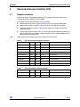
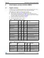
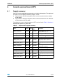
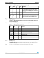
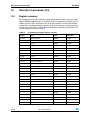
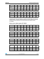
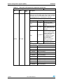
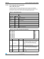
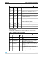
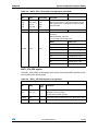
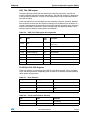
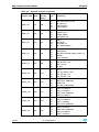
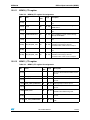
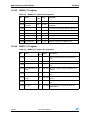
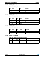
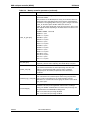
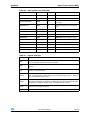
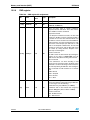
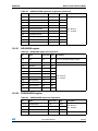
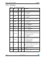
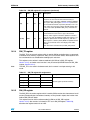
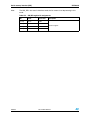
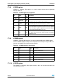
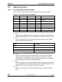
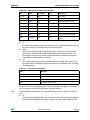
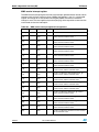
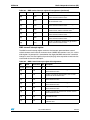
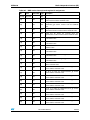
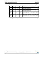
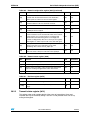
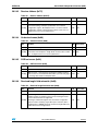
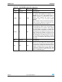
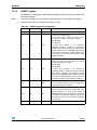
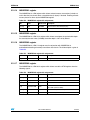
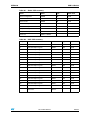
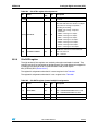
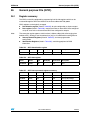
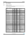
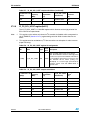
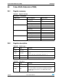
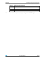
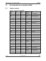
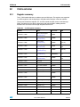
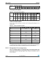
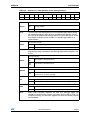
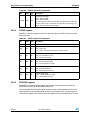
Address map
1
SPEAr320
Address map
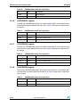
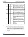
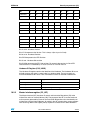
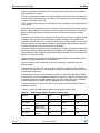
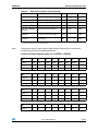
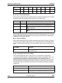
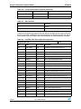
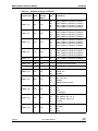
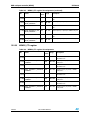
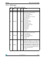
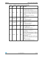
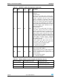
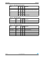
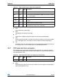
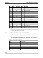
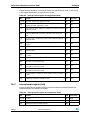
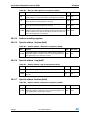
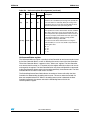
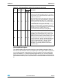
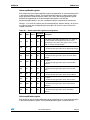
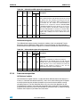
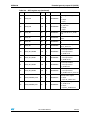
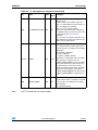
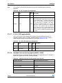
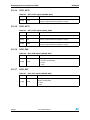
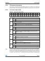
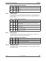
Table 2.
22/533
SPEAr320 main memory map
Start address
End address
Peripheral
Description
0x0000.0000
0x3FFF.FFFF
External DRAM
Low power DDR or DDR2
0x4000.0000
0xBFFF.FFFF
-
Reconfigurable array
subsystem (See Table 3)
0xC000.0000
0xCFFF.FFFF
-
Reserved
0xD000.0000
0xD007.FFFF
UART0
0xD008.0000
0xD00F.FFFF
ADC
0xD010.0000
0xD017.FFFF
SSP0
0xD018.0000
0xD01F.FFFF
I2C0
0xD020.0000
0xD07F.FFFF
-
0xD080.0000
0xD0FF.FFFF
JPEG CODEC
0xD100.0000
0xD17F.FFFF
IrDA
0xD180.0000
0xD1FF.FFFF
-
Reserved
0xD280.0000
0xD7FF.FFFF
SRAM
Static RAM shared
memory (8 Kbytes)
0xD800.0000
0xE07F.FFFF
-
Reserved
0xE080.0000
0xE0FF.FFFF
Ethernet controller
MAC
0xE100.0000
0xE10F.FFFF
USB 2.0 device
FIFO
0xE110.0000
0xE11F.FFFF
USB 2.0 device
Configuration registers
0xE120.0000
0xE12F.FFFF
USB 2.0 device
Plug detect
0xE130.0000
0xE17F.FFFF
-
Reserved
0xE180.0000
0xE18F.FFFF
USB2.0 EHCI 0-1
0xE190.0000
0xE19F.FFFF
USB2.0 OHCI 0
0xE1A0.0000
0xE20F.FFFF
-
0xE210.0000
0xE21F.FFFF
USB2.0 OHCI 1
0xE220.0000
0xE27F.FFFF
-
Reserved
0xE280.0000
0xE28F.FFFF
ML USB ARB
Configuration register
0xE290.0000
0xE7FF.FFFF
-
Reserved
0xE800.0000
0xEFFF.FFFF
-
Reserved
0xF000.0000
0xF00F.FFFF
Timer0
0xF010.0000
0xF10F.FFFF
-
0xF110.0000
0xF11F.FFFF
ITC Primary
0xF120.0000
0xF7FF.FFFF
-
0xF800.0000
0xFBFF.FFFF
Serial Flash memory
Doc ID 022180 Rev 1
Reserved
Reserved
Reserved
Reserved
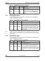
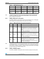
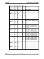
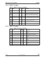
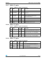
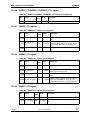
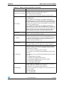
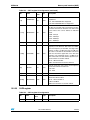
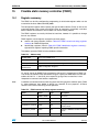
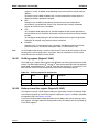
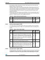
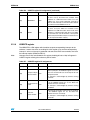
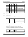
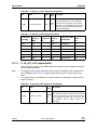
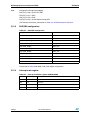
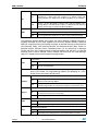
SPEAr320
Address map
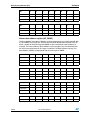
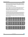
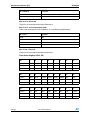
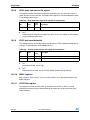
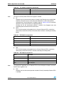
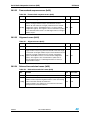
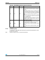
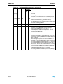
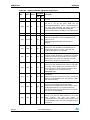
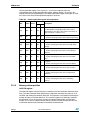
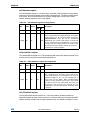
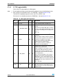
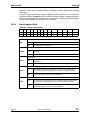
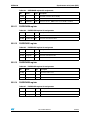
Table 2.
SPEAr320 main memory map (continued)
Start address
End address
Peripheral
0xFC00.0000
0xFC1F.FFFF
Serial Flash controller
0xFC20.0000
0xFC3F.FFFF
-
0xFC40.0000
0xFC5F.FFFF
DMA controller
0xFC60.0000
0xFC7F.FFFF
DRAM controller
0xFC80.0000
0xFC87.FFFF
Timer 1
0xFC88.0000
0xFC8F.FFFF
Watchdog timer
0xFC90.0000
0xFC97.FFFF
Real time clock
0xFC98.0000
0xFC9F.FFFF
basGPIO
0xFCA0.0000
0xFCA7.FFFF
System controller
0xFCA8.0000
0xFCAF.FFFF
Miscellaneous registers
0xFCB0.0000
0xFCB7.FFFF
Timer 2
0xFCB8.0000
0xFCFF.FFFF
-
Reserved
0xFD00.0000
0xFEFF.FFFF
-
Reserved
0xFF00.0000
0xFFFF.FFFF
BootROM
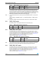
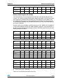
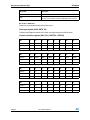
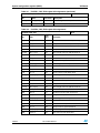
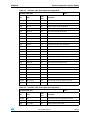
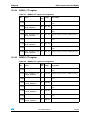
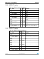
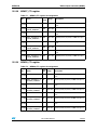
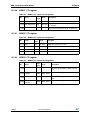
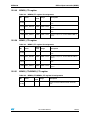
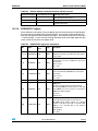
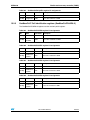
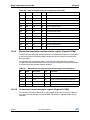
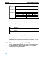
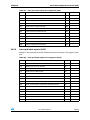
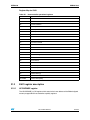
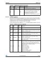
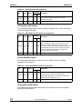
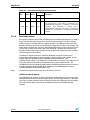
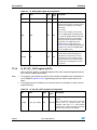
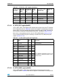
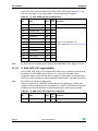
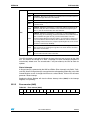
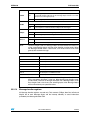
Table 3.
Description
Reserved
Reconfigurable array subsystem memory map
Start address
End address
Peripheral
0x4000_0000
0x47FF_FFFF
EMI
0x4800_0000
0x4BFF_FFFF
-
0x4C00_0000
0x5FFF_FFFF
FSMC
0x6000_0000
0x6FFF_FFFF
-
0x7000_0000
0x7FFF_FFFF
SDIO
0x8000_0000
0x8000_3FFF
Boot memory
0x8000_4000
0x8FFF_FFFF
-
0x9000_0000
0x9FFF_FFFF
CLCD
0xA000_0000
0xA0FF_FFFF
Parallel port
0xA100_0000
0xA1FF_FFFF
CAN0
0xA200_0000
0xA2FF_FFFF
CAN1
0xA300_0000
0xA3FF_FFFF
UART1
0xA400_0000
0xA4FF_FFFF
UART2
0xA500_0000
0xA5FF_FFFF
SSP1
0xA600_0000
0xA6FF_FFFF
SSP2
0xA700_0000
0xA7FF_FFFF
I2C1
0xA800_0000
0xA8FF_FFFF
Quad PWM timer
0xA900_0000
0xA9CF_FFFF
GPIO
Doc ID 022180 Rev 1
Description
Reserved
Reserved
Reserved
23/533
Address map
SPEAr320
Table 3.
24/533
Reconfigurable array subsystem memory map (continued)
Start address
End address
Peripheral
Description
0xA9D0_0000
0xA9FF_FFFF
-
Reserved
0xAA00_0000
0xAAFF_FFFF
SMII0
0xAB00_0000
0xABFF_FFFF
SMII1/MII
0xAC00_0000
0xB2FF_FFFF
-
0xB300_0000
0xBFFF_FFFF
AHB interface
Doc ID 022180 Rev 1
Reserved
SPEAr320
2
ARM926EJ-S
ARM926EJ-S
For ARM926EJ-S-related registers, refer to Chapter 11: System configuration registers
(MISC).
Doc ID 022180 Rev 1
25/533
Bus interconnection matrix
3
SPEAr320
Bus interconnection matrix
Refer to Chapter 11: System configuration registers (MISC).
26/533
Doc ID 022180 Rev 1
SPEAr320
Vectored interrupt controller (VIC)
4
Vectored interrupt controller (VIC)
4.1
Register summary
The VIC can be fully configured by programming its 32-bit wide registers which can be
accessed at the base addresses 0xF110_0000.
VIC registers can be logically divided in four main groups:
Note:
●
Interrupt control and status registers (listed in Table 4), for interrupt configuration.
●
Vector address registers (listed in Table 5), containing the address of the ISRs.
●
Vector control registers (listed in Table 6), which select the interrupt source for the
vectored interrupt.
●
Identification registers (listed in Table 7), namely eight 8 bit RO registers reporting VICspecific information (part number, revision number and so on). Refer to ARM technical
documentation for further details.
Offset addresses from 0x300 to 0x310 are reserved for test purposes.
Table 4.
VIC interrupt control registers summary
Name
Offset
Type
Reset value
Description
VICIRQSTATUS
0x000
RO
32’h0
IRQ status
VICFIQSTATUS
0x004
RO
32’h0
FIQ status
VICRAWINTR
0x008
RO
-
Raw interrupt status
VICINTSELECT
0x00C
RW
32’h0
Interrupt select
VICINTENABLE
0x010
RW
32’h0
Interrupt enable
VICINTENCLEAR
0x014
WO
-
Interrupt enable clear
VICSOFTINT
0x018
RW
32’h0
Software interrupt
VICSOFTINTCLEAR 0x01C
WO
-
Software interrupt clear
VICPROTECTION
RW
32’h0
Protection enable
Table 5.
0x020
VIC vector address registers summary
Name
Offset
Type
Reset value
Description
VICVECTADDR
0x030
RW
32’h0
Vector address
VICDEFVECTADDR
0x034
RW
32’h0
Default vector address
Doc ID 022180 Rev 1
27/533
Vectored interrupt controller (VIC)
Table 5.
SPEAr320
VIC vector address registers summary (continued)
Name
Offset
Type
Reset value
VICVECTADDR0
0x100
RW
32’h0
VICVECTADDR1
0x104
RW
32’h0
VICVECTADDR2
0x108
RW
32’h0
VICVECTADDR3
0x10C
RW
32’h0
VICVECTADDR4
0x110
RW
32’h0
VICVECTADDR5
0x114
RW
32’h0
VICVECTADDR6
0x118
RW
32’h0
VICVECTADDR7
0x11C
RW
32’h0
VICVECTADDR8
0x120
RW
32’h0
VICVECTADDR9
0x124
RW
32’h0
VICVECTADDR10
0x128
RW
32’h0
VICVECTADDR11
0x12C
RW
32’h0
VICVECTADDR12
0x130
RW
32’h0
VICVECTADDR13
0x134
RW
32’h0
VICVECTADDR14
0x138
RW
32’h0
VICVECTADDR15
0x13C
RW
32’h0
Description
Vector address registers
Table 6.
VIC interrupt vector control registers summary
Name
Offset
Type
Reset value
VICVECTCNTL0
0x200
RW
32’h0
VICVECTCNTL1
0x204
RW
32’h0
VICVECTCNTL2
0x208
RW
32’h0
VICVECTCNTL3
0x20C
RW
32’h0
VICVECTCNTL4
0x210
RW
32’h0
VICVECTCNTL5
0x214
RW
32’h0
VICVECTCNTL6
0x218
RW
32’h0
VICVECTCNTL7
0x21C
RW
32’h0
VICVECTCNTL8
0x220
RW
32’h0
VICVECTCNTL9
0x224
RW
32’h0
VICVECTCNTL10
0x228
RW
32’h0
VICVECTCNTL11
0x22C
RW
32’h0
VICVECTCNTL12
0x230
RW
32’h0
VICVECTCNTL13
0x234
RW
32’h0
VICVECTCNTL14
0x238
RW
32’h0
VICVECTCNTL15
0x23C
RW
32’h0
Description
Vector Control.
28/533
Doc ID 022180 Rev 1
SPEAr320
Vectored interrupt controller (VIC)
Table 7.
VIC identification registers summary
Name
Offset
Type
Reset value
VICPERIPHID0
0xFE0
RO
8’h90
VICPERIPHID1
0xFE4
RO
8’h11
VICPERIPHID2
0xFE8
RO
8’h04
VICPERIPHID3
0xFEC
RO
8’h00
VICPCELLID0
0xFF0
RO
8’h0D
VICPCELLID1
0xFF4
RO
8’hF0
VICPCELLID2
0xFF8
RO
8’h05
VICPCELLID3
0xFFC
RO
8’hB1
Description
Peripheral Identification.
Identification Registers
4.2
Register descriptions
4.2.1
VICIRQSTATUS register
The VICIRQSTATUS is the RO register which provides the status of interrupts after IRQ
masking (through VICINTENABLE and VICINTSELECT registers, Section 4.2.5:
VICINTENABLE register and Section 4.2.4: VICINTSELECT register respectively), at the
output of the Interrupt Request Logic block.
Table 8.
4.2.2
VICIRQSTATUS register bit assignments
Bit
Name
Reset
value
Description
[31:00]
IRQStatus
32’h0
Each bit is associated to an interrupt.
If a bit is set, it indicates that the relevant interrupt is
active, and generates an interrupt to the processor.
VICFIQSTATUS register
The VICFIQSTATUS is the RO register which provides the status of the interrupts after FIQ
masking (through VICINTENABLE and VICINTSELECT, Section 4.2.5: VICINTENABLE
register and Section 4.2.4: VICINTSELECT register respectively), at the output of the
interrupt request logic block.
Table 9.
VICFIQSTATUS register bit assignments
Bit
Name
Reset
value
Description
[31:00]
FIQStatus
32’h0
Each bit is associated to an interrupt.
If a bit is set, it indicates that the relevant interrupt is
active, and generates an interrupt to the processor.
Doc ID 022180 Rev 1
29/533
Vectored interrupt controller (VIC)
4.2.3
SPEAr320
VICRAWINTR register
The VICRAWINTR is a RO register, which provides the raw status of both interrupt sources
and software interrupts (before masking through enable registers, VICINTENABLE and
VICINTSELECT).
Table 10.
4.2.4
VICRAWINTR register bit assignments
Bit
Name
Reset
value
Description
[31:00]
Raw Interrupt
-
Each bit is associated to an interrupt.
If a bit is set, it indicates that the relevant interrupt
request is active before masking.
VICINTSELECT register
The VICINTSELECT is a RW register which allows to select whether the corresponding
interrupt generates an FIQ or an IRQ interrupt.
Table 11.
Bit
[31:00]
4.2.5
VICINTSELECT register bit assignments
Name
IntSelect
Reset
value
Description
32’h0
Each bit is associated to an interrupt line.
Each bit allows to select the type of interrupt for
relevant interrupt requests, according to encoding:
1‘b0 = IRQ interrupt
1‘b1 = FIQ interrupt
VICINTENABLE register
The VICINTENABLE is a RW register which allows to enable the interrupt request lines by
masking the interrupt sources for the IRQ interrupt.
Table 12.
Bit
[31:00]
4.2.6
VICINTENABLE register bit assignments
Name
IntEnable
Reset
value
Description
32’h0
Each bit is associated to an interrupt line.
If a bit is set, the relevant interrupt request to the
processor is enabled.
A HIGH bit sets the corresponding bit in the
VICINTENABLE Register. A LOW bit has no effect.
VICINTENCLEAR register
The VICINTENCLEAR is a WO register which allows to clear bits in the VICINTENABLE
register (Section 4.2.5: VICINTENABLE register).
30/533
Doc ID 022180 Rev 1
SPEAr320
Vectored interrupt controller (VIC)
Table 13.
Bit
[31:00]
4.2.7
VICINTENCLEAR register bit assignments
Name
IntEnableClear
Reset
value
Description
-
Each bit is associated to an interrupt line.
Writing a 1‘b1 in a bit, the corresponding bit in the
VICINTENABLE register is cleared.
Writing a 1‘b0 has no effect.
VICSOFTINT register
The VICSOFTINT (software interrupt) is a RW register which generates software interrupts.
Table 14.
4.2.8
VICSOFTINT register bit assignments
Bit
Name
Reset
value
Description
[31:00]
SoftInt
32’h0
Each bit is associated to a source interrupt.
Setting a bit, a software interrupt for the specific source
interrupt is generated before interrupt masking.
VICSOFTINTCLEAR register
The VICSOFTINTCLEAR is a WO register which allows to clear bits in the VICSOFTINT
register (Section 4.2.7: VICSOFTINT register).
Table 15.
Bit
[31:00]
4.2.9
VICSOFTINTCLEAR register bit assignments
Name
SoftIntClear
Reset
value
Description
-
Each bit is associated to an interrupt line.
Writing a 1‘b1 in a bit, the corresponding bit in the
VICSOFTINT register is cleared.
Writing a 1‘b0 has no effect.
VICPROTECTION register
The VICPROTECTION is a RW register which allows to enable or disable protected register
access.
Doc ID 022180 Rev 1
31/533
Vectored interrupt controller (VIC)
Table 16.
SPEAr320
VICPROTECTION register bit assignments
Bit
Name
Reset
value
Description
[31:01]
Reserved
-
Read: undefined. Write: should be zero.
1’h0
Enable/disable protected register access.
Setting this bit, protected register access is enabled
ensuring that only privileged mode accesses, reads
and writes, can access the interrupt controller
registers.
Clearing this bit, protected register access is disabled
allowing both user mode and privileged mode to
access the registers.
[00]
Protection
Note:
This register is cleared on reset, and it can only be accessed in privileged mode. If the AHB
master cannot generate accurate protection information, this register shall leaved in its reset
state (protection disabled) in order to enable User mode access.
4.2.10
VICVECTADDR register
The VICVECTADDR (vector address) is a RW register which contains the ISR address of
the currently active interrupt.
Table 17.
Bit
[31:00]
VICVECTADDR register bit assignments
Name
Vector Addr
Reset
value
Description
32’h0
Reading from this register provides the address of the
currently active ISR, indicating that the interrupt is
being serviced.
Writing to this register indicates that the interrupt has
been serviced and the interrupt is cleared.
Note:
The ISR reads the VICVECTADDR register when an IRQ interrupt is generated. At the end
of the ISR, the VICVECTADDR register is written to, to update the priority hardware.
Reading or writing to this register at other times can cause incorrect operation.
4.2.11
VICDEFVECTADDR register
The VICDEFVECTADDR (default vector address) is a RW register which contains the
default ISR address.
4.2.12
VICVECTADDR register
Each VICVECTADDRi (with i = 0...15) is a RW register which contains the ISR address for
the relevant vectored interrupt.
32/533
Doc ID 022180 Rev 1
SPEAr320
4.2.13
Vectored interrupt controller (VIC)
VICVECTCNTL register
Each VICVECTCNTLi (with i = 0...15) is a RW registers which allows to select the interrupt
source for the i-th vectored interrupt. The bit assignments of VICVECTCNTLi are given in
Table 18.
Table 18.
VICVECTCNTL registers bit assignments
Bit
Name
Reset
value
Description
[31:06]
Reserved
-
Read: undefined. Write: should be zero.
[05]
E
1’h0
If set, it enables vector interrupt.
[04:00]
IntSource
5’h0
It allows to select any of the 32 interrupt sources (IRQ
only).
Note:
Vectored interrupts are only generated if the interrupt is enabled. The specific interrupt is
enabled in the VICINTENABLE register (Section 4.2.5: VICINTENABLE register), and the
interrupt is set to generate an IRQ interrupt in the VICINTSELECT register (Section 4.2.4:
VICINTSELECT register). This prevents multiple interrupts being generated from a single
request if the controller is incorrectly programmed.
4.2.14
Peripheral identification registers
The read-only VICPeriphID0-3 registers are four 8 bit registers, that span address locations
0xFE0-0xFEC. You can treat the registers conceptually as a single 32 bit register. The readonly registers provide the following options for the peripheral.Table 19.
Table 19.
Bit
Name
Description
[31:24]
Configuration
This is the configuration option of the peripheral. the
configuration value is 0.
[23:20]
Revision number
This is the revision number of the peripheral. The revision
number starts from 0.
Designer
This is the identification of the designer
12 -15 Designer 0;
16 -19 Designer 1
Part number
This identifies the peripheral. The VIC uses the three-digit
product code 0x90.
0 - 7 Part number 0;
8-11 Part number 1
[19:12]
[11:00]
4.2.15
Peripheral identification registers bit assignments
VICPERIPHID0 register
The read-only VICPERIPHID0 register, with address offset of 0xFE0, is hard-coded, and the
fields within the register determine the reset value. Table 20 shows the bit assignments for
this register.
Doc ID 022180 Rev 1
33/533
Vectored interrupt controller (VIC)
Table 20.
Bit
VICPERIPHID0 register bit assignments
Name
[31:08]
[07:00]
4.2.16
SPEAr320
Description
Read undefined
Partnumber0
These bits read back as 0x90
VICPERIPHID1 register
The read-only VICPERIPHID1 register, with address offset of 0xFE4, is hard-coded, and the
fields within the register determine the reset value. Table 21 shows the bit assignments for
this register.
Table 21.
Bit
VICPERIPHID1 register bit assignments
Name
[31:08]
4.2.17
Description
Read undefined
[07:04]
Designer0
These bits read back as 0x1
[03:00]
Partnumber1
These bits read back as 0x1
VICPERIPHID2 register
The read-only VICPERIPHID2 register, with address offset of 0xFE8, is hard-coded, and the
fields within the register determine the reset value. Table 22 shows the bit assignments for
this register.
Table 22.
Bit
VICPERIPHID2 register bit assignments
Name
[31:08]
4.2.18
Description
Read undefined
[07:04]
Revision
These bits read back as 0x1
[03:00]
Designer1
These bits read back as 0x0
VICPERIPHID3 register
The read-only VICPERIPHID3 register, with address offset of 0xFEC, is hard-coded, and
the fields within the register determine the reset value.Table 23 shows the bit assignments
for this register.
Table 23.
Bit
VICPERIPHID3 register bit assignments
Name
[31:08]
[07:00]
34/533
Description
Read undefined
Configuration
These bits read back as 0x0
Doc ID 022180 Rev 1
SPEAr320
4.2.19
Vectored interrupt controller (VIC)
Identification registers
The read-only VICPCELLID0-3 registers are four 8 bit registers, that span address locations
0xFF0-0xFFC. You can treat the registers conceptually as a single 32 bit register. Use the
register as a standard cross-peripheral identification system.
4.2.20
VICPCELLID0 register
The read-only VICPCELLID0 register, with address offset 0xFF0, is hard-coded and the
fields within the register determine the reset value. Table 24 shows the bit assignments for
this register
Table 24.
Bit
VICPCELLID0 register bit assignments
Name
[31:08]
[07:00]
4.2.21
Description
Read undefined
VICPCellID0
These bits read back as 0x0D
VICPCELLID1 register
The read-only VICPCELLID1 register, with address offset 0xFF4, is hard-coded and the
fields within the register determine the reset value. Table 25 shows the bit assignments for
this register
Table 25.
Bit
VICPCELLID1 register bit assignments
Name
[31:08]
[07:00]
4.2.22
Description
Read undefined
VICPCellID1
These bits read back as 0xF0
VICPCELLID2 register
The read-only VICPCELLID2 register, with address offset 0xFF8, is hard-coded and the
fields within the register determine the reset value. Table 26 shows the bit assignments for
this register
Table 26.
Bit
VICPCELLID2 register bit assignments
Name
[31:08]
[07:00]
4.2.23
Description
Read undefined
VICPCellID2
These bits read back as 0x05
VICPCELLID3 register
The read-only VICPCELLID3 register, with address offset 0xFFC, is hard-coded and the
fields within the register determine the reset value. Table 27 shows the bit assignments for
this register
Doc ID 022180 Rev 1
35/533
Vectored interrupt controller (VIC)
Table 27.
Bit
VICPCELLID3 register bit assignments
Name
[31:08]
[07:00]
36/533
SPEAr320
Description
Read undefined
VICPCellID3
These bits read back as 0xB1
Doc ID 022180 Rev 1
SPEAr320
Direct memory access controller (DMAC)
5
Direct memory access controller (DMAC)
5.1
Register summary
The DMAC can be fully configured by programming its 32-bit wide registers which can be
accessed through the AHB slave interface at the base address 0xFC40_0000.
DMAC registers can be logically arranged in four main groups:
●
Global registers, listed in Table 28, for DMAC-level configuration,
●
Channel registers for programming a single DMA channel. Each DMA channel is
associated to these five registers, listed in Table 29 where n ranges from 0 to 7 being 8
the number of DMA channels supported by the DMAC,
●
Peripheral identification registers, listed in Table 30,
●
Cell identification registers, listed in Table 31.
Table 28.
DMAC global registers summary
Name
Offset
Type
Reset
Value
Description
DMACIntStatus
0x000
RO
32’h0
Interrupt status.
DMACIntTCStatus
0x004
RO
32’h0
Interrupt terminal count status.
DMACIntTCClear
0x008
WO
32’h0
Interrupt terminal count clear.
DMACIntErrorStatus
0x00C
RO
32’h0
Interrupt error status.
DMACIntErrClr
0x010
WO
32’h0
Interrupt error clear.
DMACRawIntTCStatus
0x014
RO
32’h0
Raw interrupt terminal count status.
DMACRawIntErrorStatus
0x018
RO
32’h0
Raw interrupt error status.
DMACEnbldChns
0x01C
RO
32’h0
Enabled channel.
DMACSoftBReq
0x020
RW
32’h0
Software burst request.
DMACSoftSReq
0x024
RW
32’h0
Software single request.
DMACSoftLBReq
0x028
RW
32’h0
Software last burst request.
DMACSoftLSReq
0x02C
RW
32’h0
Software last single request.
DMACConfiguration
0x030
RW
32’h0
DMAC configuration
DMACSync
0x034
RW
32’h0
Synchronization.
Table 29.
DMAC channel registers summary
Name
Offset
Type
Reset
Value
Description
DMACCnSrcAddr
0x100 + (n · 0x020)
RW
32’h0
Channel source address.
DMACCnDestAddr
0x104 + (n · 0x020)
RW
32’h0
Channel destination address.
DMACCnLLI
0x108 + (n · 0x020)
RW
32’h0
Channel linked list item.
DMACCnControl
0x10C + (n · 0x020)
RW
32’h0
Channel control.
DMACCnConfiguration
0x110 + (n · 0x020)
RW
32’h0
Channel configuration.
Doc ID 022180 Rev 1
37/533
Direct memory access controller (DMAC)
Table 30.
SPEAr320
DMAC peripheral registers summary
Name
Offset
Type
Description
DMACPeriphID0
0xFE0
RO
See Section 5.2.20.
DMACPeriphID1
0xFE4
RO
See Section 5.2.20.
DMACPeriphID2
0xFE8
RO
See Section 5.2.20.
DMACPeriphID3
0xFEC
RO
See Section 5.2.20.
Table 31.
DMAC cell identification registers summary
Name
Offset
Type
Description
DMACPCellID0
0xFF0
RO
See Section 5.2.21.
DMACPCellID1
0xFF4
RO
See Section 5.2.21.
DMACPCellID2
0xFF8
RO
See Section 5.2.21.
DMACPCellID3
0xFFC
RO
See Section 5.2.21.
5.2
Register description
5.2.1
DMACIntStatus register
The DMACIntStatus (interrupt status) is a RO register which shows the status of the
interrupts after masking.
Table 32.
Bit
Name
Reset value Description
[31:08]
Reserved
-
Read: undefined.
8’h00
Status of DMA interrupts after masking.
Each bit is associated to a DMA channel. If a bit is set, it
means that an interrupt request is active for the relevant
DMA channel.
[07:00]
5.2.2
DMACIntStatus register bit assignments
IntStatus
DMACIntTCStatus register
The DMACIntTCStatus (interrupt terminal count status) is a RO register which shows the
status of the terminal count after masking.
Note:
38/533
This register must be used in conjunction with the DMACIntStatus register if the combined
interrupt request, DMACINTR, is used. If the DMACINTTC interrupt request is used, reading
this register only is enough to determine source of the interrupt request.
Doc ID 022180 Rev 1
SPEAr320
Direct memory access controller (DMAC)
Table 33.
Bit
Name
Reset value Description
[31:08]
Reserved
-
Read: undefined.
8’h00
Interrupt terminal count request status.
Each bit is associated to a DMA channel. If a bit is set, it
means that an interrupt terminal count request is active for
the relevant DMA channel.
[07:00]
5.2.3
DMACIntTCStatus register bit assignments
IntTCStatus
DMACIntTCClear register
The DMACIntTCClear (interrupt terminal count clear) is a WO register which allow to clear a
terminal count interrupt request.
Table 34.
Bit
Name
Reset value Description
[31:08]
Reserved
-
[07:00]
5.2.4
DMACIntTCClear register bit assignments
Write as zero.
Terminal count request clear.
Each bit is associated to a DMA channel. When writing to
this register, each bit that is set causes the corresponding bit
in the DMACIntTCStatus register to be cleared. In contrast,
bits that are not set have no effect on the corresponding bit
in the DMACIntTCStatus register.
IntTCClear 8’h00
DMACIntErrorStatus register
The DMACIntErrorStatus (interrupt error status) is a RO register which shows the status of
the error request after masking.
Note:
This register must be used in conjunction with the DMACIntStatus register if the combined
interrupt request, DMACINTR, is used. If the DMACINTERR interrupt request is used,
reading this register only is enough to determine source of the interrupt request.
Table 35.
Bit
Name
Reset
Value
Description
[31:08]
Reserved
-
Read: undefined.
8’h00
Interrupt error status.
Each bit is associated to a DMA channel. If a bit is set, it
means that an interrupt error request is active for the
relevant DMA channel.
[07:00]
5.2.5
DMA ClntErrorStatus register bit assignments
IntErrorStatus
DMACIntErrClr register
The DMACIntErrClr (interrupt error clear) is a WO register which allow to clear an error
interrupt request.
Doc ID 022180 Rev 1
39/533
Direct memory access controller (DMAC)
Table 36.
DMACIntErrClr register bit assignments
Bit
Name
Reset value
Description
[31:08]
Reserved
-
Write as zero.
8’h00
Interrupt error request clear.
Each bit is associated to a DMA channel. When writing to
this register, each bit that is set causes the corresponding bit
in the DMACIntErrorStatus register to be cleared. In
contrast, bits that are not set have no effect on the
corresponding bit in the DMACIntErrorStatus register.
[07:00]
5.2.6
SPEAr320
IntErrClr
DMACRawIntTCStatus register
The DMACRawIntTCStatus (raw interrupt terminal count status) is a RO register which
indicates the DMA channels that are requesting a transfer complete, terminal count
interrupt, prior to masking.
Table 37.
Bit
Name
Reset value Description
[31:08]
Reserved
-
Read: undefined.
8’h00
Status of the terminal count interrupt prior to masking.
Each bit is associated to a DMA channel. If a bit is set,
it means that a terminal count interrupt request is
active prior to masking for the relevant DMA channel.
[07:00]
5.2.7
DMACRawIntTCStatus register bit assignments
RawIntTCStatus
DMACRawIntErrorStatus register
The DMACRawIntErrorStatus (raw interrupt error status) is a RO register which indicates
the DMA channels that are requesting an errror interrupt prior to masking.
Table 38.
Bit
Name
Reset value
Description
[31:08]
Reserved
-
Read: undefined.
[07:00]
5.2.8
DMACRawIntErrorStatus register bit assignments
RawIntErrorStatus 8’h00
Status of the error interrupt prior to masking.
Each bit is associated to a DMA channel. If a bit is
set, it means that an error interrupt request is active
prior to masking for the relevant DMA channel.
DMACEnbldChns register
The DMACEnbldChns (enabled channel) is a RO register which indicates the DMA
channels that are enabled, as indicated by the Enable bit (E) in the DMACCnConfiguration
register (Section 5.2.13).
40/533
Doc ID 022180 Rev 1
SPEAr320
Direct memory access controller (DMAC)
Table 39.
Bit
Name
Reset value
Description
[31:08]
Reserved
-
Read: undefined.
[07:00]
5.2.9
DMACEnbldChns register bit assignments
EnabledChannels 8’h00
Channel enable status.
Each bit is associated to a DMA channel. If a bit is
set, it means that corresponding DMA channel is
enabled. A bit is cleared on completion of the DMA
transfer.
DMACSoftBReq register
The DMACSoftBReq (software burst request) is a RW register which enables DMA burst
requests to be generated by software.
Table 40.
DMACSoftBReq register bit assignments
Bit
Name
Reset value
Description
[31:16]
Reserved
-
Read: undefined. Write as zero.
16’h0000
Software last burst request.
Each bit is associated to one out of 16 peripheral DMA
request lines. Setting a bit, a DMA last burst request for the
corresponding peripheral is generated, and the bit is cleared
when the transaction has completed. Reading this field of
the register indicates the sources that are requesting DMA
last burst transfers.
[15:00]
SoftBReq
Note:
A DMA burst request can be generated form either a peripheral or the software request
register. However, it is recommended not to use software and hardware peripheral requests
at the same time.
5.2.10
DMACSoftSReq register
The DMACSoftSReq (software single request) is a RW register which enables DMA single
requests to be generated by software.
Table 41.
DMACSoftSReq register bit assignments
Bit
Name
Reset value Description
[31:16]
Reserved
-
Read: undefined. Write as zero.
16’h0000
Software single request.
Each bit is associated to one out of 16 peripheral DMA
request lines. Setting a bit, a DMA single request for the
corresponding peripheral is generated, and the bit is cleared
when the transaction has completed. Reading this field of the
register indicates the sources that are requesting DMA single
transfers.
[15:00]
SoftSReq
Doc ID 022180 Rev 1
41/533
Direct memory access controller (DMAC)
SPEAr320
Note:
A DMA single request can be generated form either a peripheral or the software request
register. However, it is recommended not to use software and hardware peripheral requests
at the same time.
5.2.11
DMACSoftLBReq register
The DMACSoftLBReq (software last burst request) is a RW register which enables DMA last
burst requests to be generated by software.
Table 42.
DMACSoftLBReq register bit assignments
Bit
Name
Reset value Description
[31:16]
Reserved
-
Read: undefined. Write as zero.
16’h0000
Software last burst request.
Each bit is associated to one out of 16 peripheral DMA
request lines. Setting a bit, a DMA last burst request for the
corresponding peripheral is generated, and the bit is cleared
when the transaction has completed. Reading this field of
the register indicates the sources that are requesting DMA
last burst transfers.
[15:00]
SoftLBReq
Note:
A DMA last burst request can be generated form either a peripheral or the software request
register.
5.2.12
DMACSoftLSReq register
The DMACSoftLSReq (software last single request) is a RW register which enables DMA
last single requests to be generated by software.
Table 43.
DMACSoftLSReq register bit assignments
Bit
Name
Reset value
Description
[31:16]
Reserved
-
Read: undefined. Write as zero.
16’h0000
Software last single request.
Each bit is associated to one out of 16 peripheral DMA
request lines. Setting a bit, a DMA last single request for
the corresponding peripheral is generated, and the bit is
cleared when the transaction has completed. Reading this
field of the register indicates the sources that are
requesting DMA last single transfers.
[15:00]
SoftLSReq
Note:
A DMA last single request can be generated form either a peripheral or the software request
register.
5.2.13
DMAC configuration register
The DMACConfiguration is a RW register which allows to configure the operation of the
DMAC.
42/533
Doc ID 022180 Rev 1
SPEAr320
Direct memory access controller (DMAC)
Table 44.
Bit
Name
Reset value Description
[31:03]
Reserved
-
Read: undefined. Write as zero.
1’h0
AHB master 2 endianness configuration.
This bit enables to alter the endianness of the AHB master
interface 2, according to encoding:
1‘b0 = Little-endian mode.
1‘b1 = Big-endian mode.
[02]
5.2.14
DMACConfiguration register bit assignments
M2
[01]
M1
1’h0
AHB master 1 endianness configuration.
This bit enables to alter the endianness of the AHB master
interface 1, according to the same encoding as M2 (see
above).
[00]
E
1’h0
DMAC enable.
Setting this bit, the DMAC is enabled. Clearing this bit, the
DMAC is disabled reducing power consumption.
DMACSync register
The DMACSync (synchronization) is a RW register which allows to enable/disable
synchronization logic for the DMA request signals, namely DMACBREQ[15:0],
DMACSREQ[15:0], DMACLBREQ[15:0] and DMACLSREQ[15:0].
Note:
Synchronization logic must be used when the peripheral generating the DMA request runs
on a different clock to the DMAC. For peripherals running on the same clock as DMA,
disabling the synchronization logic improves the DMA request response time.
Table 45.
Bit
Name
Reset
value
Description
[31:16]
Reserved
-
Read: undefined. Write as zero.
16’h0000
DMA synchronization logic enable.
Each bit is associated to one out of 16 peripheral
DMA request lines. A cleared bit (as for default)
indicates that the synchronization logic for the
request signals is enabled. In contrast, setting the
bit the synchronization logic is disabled.
[15:00]
5.2.15
DMACSync register bit assignments
DMACSync
DMACCnSrcAddr register
The DMACCnSrcAddr (channel n source address) is a RW register which contains the
current source address (byte-aligned) of the data to be transferred over the n-th DMA
channel.
Note:
Source and destination addresses must be aligned to the source and destination widths.
Doc ID 022180 Rev 1
43/533
Direct memory access controller (DMAC)
SPEAr320
Software programs the DMACCnSrcAddr register directly before the appropriate DMA
channel is enabled. Once the corresponding DMA channel is enabled, this register is
updated:
●
As the source address is incremented,
●
By following the linked list when a complete packet of data has been transferred.
Reading the register when the DMA channel is active does not provide useful information.
This is because by the time the software has processed the value read, the channel might
have progressed. It is intended to be read-only when the channel has stopped, and in such
case, it shows the source address of the last item read.
Table 46.
5.2.16
DMACCnSrcAddr register bit assignments
Bit
Name
Reset value
Description
[31:00]
SrcAddr
32’h0
DMA source address.
DMACCnDestAddr register
The DMACCnDestAddr (channel n destination address) is a RW register which contains the
current destination address (byte-aligned) of the data to be transferred over the n-th DMA
channel.
Note:
Source and destination addresses must be aligned to the source and destination widths.
Software programs the DMACCnDestAddr register directly before the appropriate DMA
channel is enabled. Once the corresponding DMA channel is enabled, this register is
updated:
●
as the destination address is incremented,
●
by following the linked list when a complete packet of data has been transferred.
Reading the register when the DMA channel is active does not provide useful information.
This is because by the time the software has processed the value read, the channel might
have progressed. It is intended to be read-only when the channel has stopped, and in such
case, it shows the source address of the last item read.
Table 47.
5.2.17
DMACCnDestAddr register bit assignments
Bit
Name
Reset value Description
[31:00]
DestAddr
32’h0
DMA destination address.
DMACCnLLI register
The DMACCnLLI (channel n linked list item) is a RW register which contains the address
(word-aligned) of the next Linked List Item (LLI). If next LLI is 0, then the current LLI is the
last in the chain, and the DMA channel is disabled after all DMA transfers associated with it
are completed.
Note:
44/533
Programming this register when the corresponding DMA channel is enabled has
unpredictable results.
Doc ID 022180 Rev 1
SPEAr320
Direct memory access controller (DMAC)
Table 48.
Bit
Name
Reset value
Description
[31:02]
LLI
30’h0
Next LLI address.
This field contains the bits [31:2] of the address for the next
LLI. Address LSB bits [1:0] are 1‘b0 both.
[01]
Reserved
-
Read: undefined. Write as zero.
1’h0
AHB master select.
This bit allows to select the AHB master for loading the next
LLI, according to encoding:
1‘b0 = AHB master 1.
1‘b1 = AHB master 2.
[00]
5.2.18
DMACCnLLI register bit assignments
LM
DMACCn control register
The DMACCnControl is a RW register which contains control information about the DMA
channel n, such as transfer size, burst size and transfer width.
Software programs the DMACCnControl register directly before the appropriate DMA
channel is enabled. Once the corresponding DMA channel is enabled, this register is
updated by following the linked list when a complete packet of data has been transferred.
Reading the register when the DMA channel is active does not provide useful information.
This is because by the time the software has processed the value read, the channel might
have progressed. It is intended to be read-only when the channel has stopped.
Table 49.
DMACCnControl register bit assignments
Bit
Name
Reset value Description
[31]
I
1’h0
Terminal count interrupt enable.
This bit controls whether the current LLI is expected to trigger
the terminal count interrupt.
[30:28]
Port
3’h0
Protection.
This 3 bits field reports AHB access information which are
primarily intended to be used by source and destination
peripherals for implementing some level of protection. This field
directly controls the AHB HPROT[3:1] signals, and bit
assignment is given:
[28], HPROT[1] = 1‘b0 user mode
[28], HPROT[1] = 1‘b1 privileged mode
[29], HPROT[2] = 1‘b0 non-bufferable
[29], HPROT[2] = 1‘b1 bufferable
[30], HPROT[3] = 1‘b0 non-cacheable
[30], HPROT[3] = 1‘b1 cacheable
[27]
DI
1’h0
Destination increment.
If the bit is set, the destination (resp. source) address is
incremented after each transfer.
[26]
SI
1’h0
Source increment.
If the bit is set, the destination (resp. source) address is
incremented after each transfer.
Doc ID 022180 Rev 1
45/533
Direct memory access controller (DMAC)
Table 49.
Bit
[25]
[24]
[23:21]
[20:18]
46/533
SPEAr320
DMACCnControl register bit assignments (continued)
Name
D
S
Dwidth
Swidth
Reset value Description
1’h0
Destination AHB master select.
This bit allows to select the AHB master for the destination
(resp. source) transfer, according to encoding:
1‘b0 = AHB master 1.
1‘b1 = AHB master 2.
1’h0
Source AHB master select.
This bit allows to select the AHB master for the destination
(resp. source) transfer, according to encoding:
1‘b0 = AHB master 1.
1‘b1 = AHB master 2.
3’h0
Destination transfer width.
This 3 bits field states the width of destination (resp. source)
transfer, according to encoding:
3‘b000 = Byte (8 bit)
3‘b001 = Halfword (16 bit)
3‘b010 = Word (32 bit)
3‘b011 to 3‘b111 = Reserved
The hardware automatically packs and unpacks the data when
required.
Note: Transfers wider than the AHB master bus width are illegal.
Besides, the source and the destinations widths can be different
from each other.
3’h0
Source transfer width.
This 3 bits field states the width of destination (resp. source)
transfer, according to encoding:
3‘b000 = Byte (8 bit)
3‘b001 = Halfword (16 bit)
3‘b010 = Word (32 bit)
3‘b011 to 3‘b111 = Reserved
The hardware automatically packs and unpacks the data when
required.
Note: Transfers wider than the AHB master bus width are illegal.
Besides, the source and the destinations widths can be different
from each other.
Doc ID 022180 Rev 1
SPEAr320
Direct memory access controller (DMAC)
Table 49.
Bit
[17:15]
[14:12]
[11:00]
DMACCnControl register bit assignments (continued)
Name
Reset value Description
DBSize 3’h0
Destination burst size.
This 3 bits field indicates the number of transfers that make up a
destination (resp. source) burst transfer request, according to
the encoding:
3‘b000 = 1
3‘b001 = 4
3‘b010 = 8
3‘b011 = 16
3‘b100 = 32
3‘b101 = 64
3‘b110 = 128
3‘b111 = 256
This value must be set to the burst size of the destination (resp.
source) peripheral, being the burst size the amount of data that
is transferred when the n-th DMACBREQ signal goes active in the
destination (resp. source) peripheral. In case destination (resp.
source) is the memory, this value must be set to the memory
boundary size.
Note: Burst equal or greater than 32 are available only using
data-width 32. The data-width 8 and 16 support only bursts of
1,4,8 & 16.
SBSize 3’h0
Source burst size.
This 3 bits field indicates the number of transfers that make up a
destination (resp. source) burst transfer request, according to
the encoding:
3‘b000 = 1
3‘b001 = 4
3‘b010 = 8
3‘b011 = 16
3‘b100 = 32
3‘b101 = 64
3‘b110 = 128
3‘b111 = 256
This value must be set to the burst size of the destination (resp.
source) peripheral, being the burst size the amount of data that
is transferred when the n-th DMACBREQ signal goes active in the
destination (resp. source) peripheral. In case destination (resp.
source) is the memory, this value must be set to the memory
boundary size.
Transfer
12’h0
Size
Transfer size.
A write to this field sets the size of the transfer in case the
DMAC is the flow controller. This value counts down from the
original value to zero, and a read from this field provides then
the number of transfers still to be completed on the destination
bus.
Note: This field should be set to zero if the DMAC is not the flow
controller, avoiding then the DMAC might attempt to use a nonzero value instead of ignoring the field.
Doc ID 022180 Rev 1
47/533
Direct memory access controller (DMAC)
5.2.19
SPEAr320
DMAC Configuration register
The DMAC Configuration is a RW register which allow to configure the relevant DMA
channel.
Table 50.
Bit
Name
Reset value Description
[31:19]
Reserved
-
Read: undefined. Write as zero.
1’h0
Halt.
Setting this bit, extra source DMA requests are ignored
(otherwise enabled), and the content of channel FIFO is
drained. This bit can be jointly used with the active bit (A field
in this register) and the channel enable bit (E field in this
register) to cleanly disable a DMA channel.
1’h0
Active (read-only).
If this read-only field is set, it means that there is still data in
the channel FIFO. This bit can be jointly used with the halt bit
(H field in this register) and the channel enable bit (E field in
this register) to cleanly disable a DMA channel.
[18]
[17]
48/533
DMAC Configuration register bit assignments
H
A
[16]
L
1’h0
Lock.
Setting this bit, locked transfers are enabled: when a burst
occurs, the HLOCK signal is asserted by the DMAC, so that
the AHB arbiter doesn’t degrant the DMAC during the burst
until the lock is deasserted, even if another master with
greater priority requests the bus.
[15]
ITC
1’h0
Terminal count interrupt mask.
Clearing this bit, it masks out the terminal count interrupt for
this DMA channel.
[14]
IE
1’h0
Error interrupt mask.
Clearing this bit, it masks out the error interrupt for this DMA
channel.
[13:11]
FlowCntrl
3’h0
Flow control and transfer type.
This 3 bits field indicates both the flow controller (DMAC,
destination peripheral or source peripheral) and the transfer
type (memory-to-memory, memory-to-peripheral, …),
according to encoding:
3‘b000 = Memory-to-memory, DMAC
3‘b001 = Memory-to-peripheral, DMAC
3‘b010 = Peripheral-to-memory, DMAC
3‘b011 = Source periph.-to-destination periph., DMAC
3‘b100 = Source periph.-to-destination periph., Destination
peripheral
3‘b101 = Memory-to-peripheral, Peripheral
3‘b110 = Peripheral-to-memory, Peripheral
3‘b111 = Source periph.-to-destination periph. Source
peripheral, DestPeripheral,
[10]
Reserved
-
Read: undefined. Write as zero.
Doc ID 022180 Rev 1
SPEAr320
Direct memory access controller (DMAC)
Table 50.
Bit
Name
Reset value Description
[09:06]
DestPeriph
4’h0
eral
Destination peripheral.
This 4 bits field allows to select the DMA destination (resp.
source) request peripheral. The value is ignored in case the
destination (resp. source) of the transfer is the memory.
Note: The DestPeripheral and SrcPeripheral fields are the
binary value of the request line (4’h0 to 4’hF, that is 0 to 15)
and not a mask value.
[05]
Reserved
Read: undefined. Write as zero.
[04:01]
[00]
5.2.20
DMAC Configuration register bit assignments (continued)
-
SrcPeriphe
4’h0
ral
Source peripheral.
This 4 bits field allows to select the DMA destination (resp.
source) request peripheral. The value is ignored in case the
destination (resp. source) of the transfer is the memory.
Note: The DestPeripheral and SrcPeripheral fields are the
binary value of the request line (4’h0 to 4’hF, that is 0 to 15)
and not a mask value.
E
Channel enable.
Setting this bit, the relevant DMA channel is enabled. When
this bit is cleared, the current AHB transfer – if any – is firstly
completed (losing any data in the channel FIFO), then the
channel is disabled.
Note: Restarting the DMA channel by setting back the E bit
results in unpredictable effects and the channel must be fully
re-initialized.
If a DMA channel has to be disabled without losing data in its
channel’s FIFO, at first the Halt bit must be set, so that
subsequent DMA requests are ignored. Then, the Active bit
must be polled until it reaches 1‘b0, indicating that there is no
data left in the channel’s FIFO. Finally, the Channel Enable
bit can be cleared.
The DMA channel is also disabled (and the E bit cleared)
when either the last LLI is reached or if a channel error is
encountered.
Reading this bit indicates whether the DMA channel is
enabled or disabled.
1’h0
DMACPeriphID register
The DMACPeriphID are four 8 bit RO registers, which can be treated conceptually as a
single 32 bit register. These read-only registers provide the following peripheral options:
●
PartNumber[11:00] - This identifies the peripheral. The three digit product code 0x080
is used.
●
Designer ID[19:12] - This is the identification of the designer. ARM Limited is 0x41
(ASCII A).
●
Revision[23:20] - This is the revision number of the peripheral. The revision number
starts from 0.
●
Configuration[31:24] - This is the configuration option of the peripheral.
Doc ID 022180 Rev 1
49/533
Direct memory access controller (DMAC)
5.2.21
SPEAr320
DMACPCellID register
The DMACPCellID are four 8 bit RO registers, which can be treated conceptually as a single
32 bit register. The register is a standard cross-peripheral identification system. The
DMACPCellID register is set to 0xB105_F00D.
50/533
Doc ID 022180 Rev 1
SPEAr320
General purpose timers (GPT)
6
General purpose timers (GPT)
6.1
Register summary
Each GPT can be configured by programming a set of 16-bit wide registers. The registers of
the three GPTs are mapped in memory by couples, namely:
●
The local timer in the CPU subsystems, which can be accessed at the base address
0xF000_0000.
●
The two timers in the basic subsystem, which can be accessed at the base addresses
0xFC80_0000 and 0xFCB0_0000.
The registers are same for both the couples of GPTs and are listed in Table 51. Section 6.2
describes the registers of a generic GPT.
Table 51.
Couple of GPTs registers summary
Name
Offset
Type
Reset
Value
Description
TIMER_CONTROL1
0x0080
RW
16’h0000
Control register of 1st timer in the
couple (GPT0 or GPT2).
TIMER_STATUS_INT_ACK1 0x0084
RW
16’h0000
Status register of 1st timer.
TIMER_COMPARE1
0x0088
RW
16’hFFFF
Compare register of 1st timer.
TIMER_COUNT1
0x008C RO
16’h0000
Count register of 1st timer.
TIMER_REDG_CAPT1
0x0090
RO
16’h0000
Rising edge capture register of 1st
timer.
TIMER_FEDG_CAPT1
0x0094
RO
16’h0000
Falling edge capture register of 1st
timer.
TIMER_CONTROL2
0x0100
RW
16’h0000
Control register of 2nd timer in the
couple (GPT1 or GPT3).
TIMER_STATUS_INT_ACK2 0x0104
RW
16’h0000
Status register of 2nd timer.
TIMER_COMPARE2
0x0108
RW
16’hFFFF
Compare register of 2nd timer.
TIMER_COUNT2
0x010C RO
16’h0000
Count register of 2nd timer.
TIMER_REDG_CAPT2
0x0110
RO
16’h0000
Rising edge capture register of 2nd
timer.
TIMER_FEDG_CAPT2
0x0114
RO
16’h0000
Falling edge capture register of 2nd
timer.
Doc ID 022180 Rev 1
51/533
General purpose timers (GPT)
SPEAr320
6.2
Register description
6.2.1
Timer_control register
Table 52.
Bit
Name
Reset value
Description
[15:11]
Reserved
-
Read: undefined. Write: should be zero.
[10]
REDGE_INT
1’h0
If set, it enables interruption on a rising edge capture.
[09]
FEDGE_INT
1’h0
If set, it enables interruption on a falling edge capture.
[08]
MATCH_INT
1’h0
If set, it enables interruption when comparator matches.
2’h0
Capture mode.
This 2 bit field indicates the mode of capture, according to
encoding.
2‘b00 = No capture.
2‘b01 = Capture in rising edge.
2‘b10 = Capture in falling edge.
2‘b11 = Capture in bit edges.
1’h0
Timer enable.
Setting this bit, the GPT is enabled. Once enabled, an
initialization phase is performed before starting to count,
and capture registers (TIMER_REDG_CAPT and
TIMER_FEDG_CAPT) and counter register
(TIMER_COUNT) are cleared.
Clearing this bit, the GPT is disabled, and capture as well
as counter registers are frozen. After reset the GPT is
disabled and all interrupt sources are masked.
[07:06]
[05]
CAPTURE
ENABLE
[04]
MODE
1’h0
Operation mode.
This bit allows to select the operation mode of the GPT,
according to encoding.
1‘b0 = Auto-reload mode.
1‘b1 =Single-shot.
[03:00]
PRESCALER
4’h0
Prescaler configuration.
This 4 bit field controls the prescaler configuration,
according to encoding.
Table 53.
52/533
Timer_Control register bit assignments
PRESCALER configuration
Value
Division Scale
Frequency [MHz] Resolution [ns]
Max time [ms]
4‘b0000
1
66.5
15.04
0.971
4‘b0001
2
33.25
30.08
1.971
4‘b0010
4
16.625
60.15
3.942
4‘b0011
8
8.313
120.30
7.884
4‘b0100
16
4.156
240.20
15.768
4‘b0101
32
2.078
481.20
31.538
Doc ID 022180 Rev 1
SPEAr320
General purpose timers (GPT)
Table 53.
PRESCALER configuration
Value
Division Scale
Frequency [MHz] Resolution [ns]
Max time [ms]
4‘b0110
64
1.039
962.41
63.071
4‘b0111
128
0.520
1924.81
126.143
4‘b1000
256
0.260
3849.62
252.285
4‘b1001 to
4‘b1111
Not allowed
Not allowed
Not allowed
Not allowed
Note:
This table just illustrates the use of prescaler and its different value on a particular Input
Frequency. The table in this shows the value with 66.5 MHz as Timer clock.Timer Max
period = (65536 xTimer Resolution).
6.2.2
TIMER_STATUS_INT_ACK register
The TIMER_STATUS_INT_ACK (Status and Interrupt Acknowledge Timer) is a RW register
which indicates the raw interrupt sources status, prior to any masking.
Table 54.
TIMER_STATUS_INT_ACK register bit assignments
Bit
Name
Reset value Description
[15:03]
Reserved
13’h0
Read undefined. Write: should be zero.
1’h0
Rising edge capture.
Reading this bit as 1‘b1, it means that a rising edge has
been detected on the capture input and an interrupt is
raised.
Writing 1‘b1, the interrupt source is cleared, whereas there
is no effect when writing 1‘b0.
1’h0
Falling edge capture.
Reading this bit as 1‘b1, it means that a falling edge has
been detected on the capture input and an interrupt is
raised.
Writing 1‘b1, the interrupt source is cleared, whereas there
is no effect when writing 1‘b0.
1’h0
Match status.
Reading this bit as 1‘b1, it means that a match has occurred
in the compare unit and an interrupt is raised.
Writing 1‘b1, the interrupt source is cleared, whereas there
is no effect when writing 1‘b0.
[02]
[01]
[00]
REDGE
FEDGE
MATCH
Note:
Independently by the timer activity, pending interruptions remain active until they have been
acknowledged (writing a 1‘b1 in the relevant bit) and they are not automatically deactivated
when the timer is disabled or enabled. It is therefore strongly recommended to acknowledge
all active interrupt sources before enabling a timer.
6.2.3
TIMER_COMPARE register
The TIMER_COMPARE is a RW register allows the software to program the timer period.
Doc ID 022180 Rev 1
53/533
General purpose timers (GPT)
Table 55.
SPEAr320
TIMER_COMPARE register bit assignments
Bit
Name
Reset value
Description
[15:00]
COMPARE_VALUE
16’hFFFF
Compare value.
The COMPARE_VALUE is expressed as an integer number of clock periods (where the
input clock of the timer is the output of the prescaler) ranging from the 16’h0001 minimum
value to the 16’hFFFF maximum value (default, to be intended as free-running timer in autoreload mode). When the counter reaches the COMPARE_VALUE, the GPT behaves
depending on the operation mode (auto-reload or single-shot).
Note:
1
In auto-reload mode, when the counter reaches the COMPARE_VALUE, it is cleared and
restarts:
TIMER_PERIOD = (COMPARE_VALUE - 1) x COUNTER_PERIOD + 2 TIMER_CLOCK
periods.
2
6.2.4
COUNTER_PERIOD is the period of the timer’s input clock (i.e. the prescaler’s output).
TIMER_COUNT register
The TIMER_COUNT is a RO register indicates the current counter value.
Table 56.
6.2.5
TIMER_COUNT register bit assignments
Bit
Name
Reset value Description
[15:00]
CONT_VALUE
16’h0000
Current counter value.
TIMER_REDG_CAPT register
The TIMER_REDG_CAPT (timer rising edge capture) is a RO register which is used to
store the current value of the timer counter when a rising edge occurs. When a capture has
occurred, the REDGE bit is set in the TIMER_STATUS_INT_ACK register (Section 6.2.2)
and the corresponding interrupt, if enabled (REDGE_INT bit set to 1‘b1 in
TIMER_CONTROL register, Section 6.2.1), is raised.
Table 57.
TIMER_REDG_CAPT register bit assignments
Reset
value
Bit
Name
[15:00]
COUNT_VALUE_REDGE 16’h0000
Description
Current value of timer when a rising edge occurs
Note:
In the interrupt service routine, the capture register must be read before the next capture
event occurs: if not the current capture value will be overwritten by the next one.
6.2.6
TIMER_FEDG_CAPT register
The TIMER_FEDG_CAPT (timer falling edge capture) is a RO register which is used to
store the current value of the counter when a falling edge occurs. When a capture has
occurred, the FEDGE bit is set in the TIMER_STATUS_INT_ACK register (Section 6.2.2)
and the corresponding interrupt, if enabled (FEDGE_INT bit set to 1‘b1 in
TIMER_CONTROL register, Section 6.2.1), is raised.
54/533
Doc ID 022180 Rev 1
SPEAr320
General purpose timers (GPT)
Table 58.
Note:
TIMER_FEDG_CAPT register bit assignments
Bit
Name
Reset
value
Description
[15:00]
CONT_VALUE_FEDGE
16’h0000
Current value of timer when a falling edge occurs
In the interrupt service routine, the capture register must be read before the next capture
event occurs: if not the current capture value will be overwritten by the next one.
Doc ID 022180 Rev 1
55/533
Real-time clock (RTC)
SPEAr320
7
Real-time clock (RTC)
7.1
Register summary
The RTC can be fully configured by programming its 32-bit wide registers (listed in Table 59)
which can be accessed at the base address 0xFC90_0000.
Table 59.
RTC functional registers summary
Name
Offset
Type Reset value
Description
TIME
0x000
RW
Undefined
Time register
DATE
0x004
RW
Undefined
Date register
ALARM TIME
0x008
RW
Undefined
Alarm time register
ALARM DATE
0x00C
RW
Undefined
Alarm date register
CONTROL
0x010
RW
Undefined
Control register
STATUS
0x014
RW
Undefined
Status register
REG1MC
0x018
RW
Undefined
General purpose register
REG2MC
0x01C
RW
Undefined
General purpose register
7.2
Register description
7.2.1
CONTROL register
The CONTROL is a RW register which allows the software to control the RTC.
Table 60.
Bit
56/533
CONTROL register bit assignments
Name
Reset
value
Description
Interrupt event enable.
Setting this bit, interrupt event is enabled, and interrupts
generated by alarm logic are sent out (see ALARM TIME and
ALARM DATE registers).
[31]
IE
[30:10]
Reserved
[09]
TB
Time bypass (for testing purpose only).
[08]
PB
Prescaler bypass (for testing purpose only).
-
Read: undefined. Write: should be zero.
Doc ID 022180 Rev 1
SPEAr320
Real-time clock (RTC)
Table 60.
Bit
Name
Reset
value
Description
[07:06]
Reserved
-
Read: undefined. Write: should be zero.
[05:00]
7.2.2
CONTROL register bit assignments (continued)
Force time-calendar comparisons.
Each bit of this 6 bit field allows to mask one time-calendar
element (seconds, minutes, hours, days, months, years),
according to encoding. The aim is to generate an interrupt for
any masked element, apart from actual matching of
programmed alarms.
[00] = Seconds.
[01] = Minutes.
[02] = Hours.
[03] = Days.
[04] = Months.
[05] = Years.
MASK
STATUS register
The STATUS is a RW register (with some RO field) which indicates the status of the RTC
and allows to clear any pending interrupt.
Table 61.
Bit
STATUS register bit assignments
Name
[31]
I
[30:06]
Reserved
[05]
[04]
[03]
LD
LT
PD
Reset
value
-
Type
Description
RW
Interrupt status.
Reading from this 1 bit field, the interrupt status returns.
Writing 1‘b1 to this bit clears any pending interrupts,
whereas there is no effect writing 1‘b0.
-
Read: undefined. Write: should be zero.
RO
Write to DATE register lost.
If a second write to DATE register is requested before
the first is completed, this second request is aborted and
the LD bit is set. This bit is cleared when a write to DATE
register is performed successfully.
RO
Write to TIME register lost.
If a second write to TIME register is requested before the
first is completed, this second request is aborted and the
LT bit is set. This bit is cleared when a write to TIME
register is performed successfully.
RO
Pending write to DATE register.
If set, this bit indicates that a write to DATE register
request is asserted from 48 MHz part to 32 kHz part. It is
independent from PT. A new write can be successfully
requested only when this bit is cleared.
Doc ID 022180 Rev 1
57/533
Real-time clock (RTC)
Table 61.
Bit
STATUS register bit assignments (continued)
Name
[02]
PT
[01]
Reserved
[00]
7.2.3
SPEAr320
Reset
value
-
RC
Type
Description
RO
Pending write to TIME register.
If set, this bit indicates that a write to TIME register
request is asserted from 48 MHz part to 32 kHz part. A
new write can be successfully requested only when this
bit is cleared.
-
Read: undefined. Write: should be zero.
RO
Isolation of timer
If cleared (1‘b0), the RTC is self-isolated from the rest of
the chip. Reading and writing to TIME and DATE
registers can be safely done when this bit is set only.
TIME register
The TIME is a RW register which defines the time (hour, minutes, seconds) when the RTC
can start to count the time.
Note:
All values in this TIME register are in binary-coded decimal (BCD) format.
Table 62.
7.2.4
TIME register bit assignments
Bit
Name
Reset
value
Description
[31:22]
Reserved
-
Read: undefined. Write: should be zero.
[21:20]
HT
Current hours tens.
[19:16]
HU
Current hours units.
[15]
Reserved
[14:12]
MT
Current minutes tens.
[11:08]
MU
Current minutes units.
[07]
Reserved
[06:04]
ST
Current seconds tens.
[03:00]
SU
Current seconds units.
-
-
Read: undefined. Write: should be zero.
Read: undefined. Write: should be zero.
DATE register
The DATE is a RW register which defines the date (year, month, day) when the RTC can
start to count the time.
Note:
58/533
All values in this DATE register are in binary-coded decimal (BCD) format.
Doc ID 022180 Rev 1
SPEAr320
Real-time clock (RTC)
Table 63.
7.2.5
DATE register bit assignments
Reset
value
Bit
Name
[31:28]
YM
Current year millenniums.
[27:24]
YH
Current year hundreds.
[23:20]
YT
Current year tens.
[19:16]
YU
Current year units.
[15]
Reserved
[14:12]
MT
Current month tens.
[11:08]
MU
Current month units.
[07:06]
Reserved
[05:04]
DT
Current day tens.
[03:00]
DU
Current day units.
-
Description
Read: undefined. Write: should be zero.
-
Read: undefined. Write: should be zero.
ALARM TIME registers
The ALARM TIME is a RW register which defines a successive time, so that when the value
of TIME register is equal to the value set in this ALARM TIME register, an interrupt is
generated (if enabled, that is if IE bit in CONTROL register is set).
Note:
All values in this ALARM TIME register are in binary-coded decimal (BCD) format.
Table 64.
7.2.6
ALARM TIME register bit assignments
Bit
Name
Reset
value
Description
[31:22]
Reserved
-
Read: undefined. Write: should be zero.
[21:20]
HT
Target hour tens.
[19:16]
HU
Target hour units.
[15]
Reserved
[14:12]
MT
Target minute tens.
[11:08]
MU
Target minute units.
[07]
Reserved
[06:04]
ST
Target second tens.
[03:00]
SU
Target second units.
-
Read: undefined. Write: should be zero.
-
Read: undefined. Write: should be zero.
ALARM DATE registers
The ALARM DATE is a RW register which defines a successive date, so that when the value
of DATE register is equal to the value set in this ALARM DATE register, an interrupt is
generated (if enabled, that is if IE bit in CONTROL register is set).
Note:
All values in this ALARM DATE register are in binary-coded decimal (BCD) format.
Doc ID 022180 Rev 1
59/533
Real-time clock (RTC)
Table 65.
7.2.7
SPEAr320
ALARM DATE register bit assignments
Reset
value
Bit
Name
[31:28]
YM
Target year millenniums.
[27:24]
YH
Target year hundreds.
[23:20]
YT
Target year tens.
[19:16]
YU
Target year units.
[15]
Reserved
[14:12]
MT
Target month tens.
[11:08]
MU
Target month units.
[07:06]
Reserved
[05:04]
DT
Target day tens.
[03:00]
DU
Target day units.
-
-
Description
Read: undefined. Write: should be zero.
Read: undefined. Write: should be zero.
REGxMC register
These general purpose registers, battery powered, can be used to store information when
the system goes in a deep power saving state like suspend to ram. During this state only the
DDR memory is powered and all the other parts of the system (SOC included) are
completely off.
Table 66.
Bit
Name
[31:00]
REG1MC
Table 67.
60/533
REG1MC registers bit assignments
Reset value Description
General purpose bits
REG2MC register bit assignments
Bit
Name
[31:00]
REG2MC
Reset value Description
General purpose bits
Doc ID 022180 Rev 1
SPEAr320
System controller
8
System controller
8.1
Register summary
The system controller can be fully configured by programming its registers which can be
accessed at the base address 0xFCA0_0000
System controller registers can be logically arranged in two main groups:
Note:
●
Control and status registers, CSRs (listed in Table 68), for system controller
configuration,
●
Identification registers (listed in Table 69), namely twelve 8 bit RO registers (which can
be treated as three 32 bit registers) reporting system information and system controllerspecific information. Refer to ARM technical documentation for further details.
In addition to reserved locations within the CSRs address space (Table 68), offset
addresses from 0xF00 to 0xFDC are reserved for test purposes. All these locations must not
be used during normal operation.
Table 68.
System controller control and status registers summary
Name
Offset
Width
[bit](1)
Type
Reset
value
SCCTRL
0x000
24
RW
24’h000009 System control
SCSYSSTAT
0x004
32
RW
-
System status
SCIMCTRL
0x008
8
RW
8’h00
Interrupt mode control
SCIMSTAT
0x00C
1
RW
1’h0
Interrupt mode status
SCXTALCTRL
0x010
19
RW
19’h0
Crystal control
SCPLLCTRL
0x014
28
RW
28’h0
PLL control
-
0x018 to 0xEDC
-
-
-
Reserved
Description
1. This value represents the actual number of used bits, being reserved the others to 32.
Table 69.
System controller identification registers summary
Name
Offset
Width[bit]
Type
Reset Value
SCSYSID0
0xEE0
8
RO
8’h00
SCSYSID1
0xEE4
8
RO
8’h00
SCSYSID2
0xEE8
8
RO
-
SCSYSID3
0xEEC
8
RO
-
-
0xEF0 to
0xEFC
-
-
-
SCPeriphID0
0xFE0
8
RO
8’h10
SCPeriphID1
0xFE4
8
RO
8’h18
SCPeriphID2
0xFE8
8
RO
8’h04
SCPeriphID3
0xFEC
8
RO
8’h00
Description
System identification
Reserved
Peripheral identification
Doc ID 022180 Rev 1
61/533
System controller
Table 69.
SPEAr320
System controller identification registers summary (continued)
Name
Offset
Width[bit]
Type
Reset Value
SCPCellID0
0xFF0
8
RO
8’h0D
SCPCellID1
0xFF4
8
RO
8’hF0
SCPCellID2
0xFF8
8
RO
8’h05
SCPCellID3
0xFFC
8
RO
8’hB1
Description
Identification Registes
8.2
Register description
8.2.1
SCCTRL register
The SCCTRL (control) is a RW register which is used to define the required operation of the
system controller.
Table 70.
62/533
SCCTRL register bit assignments
Bit
Name
Reset
value
Description
[31:24]
Reserved
-
Read: undefined. Write: should be zero
[23]
WDogEnOv
1’h0
Watchdog enable override
This bit allows to control the watchdog enable output
signal, according to the encoding:
1‘b0 = Derived from REFCLK clock source,
1‘b1 = Forced high
[22:21]
Reserved
-
Read: undefined. Write: should be zero
[20]
TimerEn2Ov
1’h0
Timer enable 2, override
[19]
TimerEn2Sel
1’h0
Timer enable 2, timing reference select
[18]
TimerEn1Ov
1’h0
Timer enable 1, override
If set, this bit forces high the timer enable output
signal. Otherwise the bit is cleared.
Timer enable 1, timing reference select
This bit allows to select the reference clock for the
timer enable signals, according to the encoding:
1‘b0 = REFCLK
1‘b1 = TIMCLK
[17]
TimerEn1Sel
1’h0
[16]
TimerEn0Ov
1’h0
Timer enable 0, override
[15]
TimerEn0Sel
1’h0
Timer enable 0, timing reference select
[14:12]
HCLKDivSel
3’h0
Control the HCLKDIVSEL output
[11:10]
Reserved
-
Read: undefined. Write: should be zero
[09]
RemapStat
1’h0
Remap status
This bit is used to return the value of the
REMAPSTAT input.
Doc ID 022180 Rev 1
SPEAr320
System controller
Table 70.
Bit
Name
Reset
value
Description
[08]
RemapClear
1’h0
Remap clear request
This bit is used to control the REMAPCLEAR output.
Setting this bit indicates that the memory remap will
be cleared.
[07]
Reserved
-
Read: undefined. Write: should be zero
4’h01
Mode status bitsThis 4 bit field returns the current
operation mode as defined by the system controller
state machine, according to the encoding:
4‘b0000 = SLEEP
4‘b0001 = DOZE (reser value)
4‘b0010 = SLOW
4‘b0011 = XTAL CTL
4‘b0100 = NORMAL
4‘b0101 = Not used
4‘b0110 = PLL CTL
4‘b0111 = Not used
4‘b1000 = Not used
4‘b1001 = SW from XTAL
4‘b1010 = SW from PLL
4‘b1011 = SW to XTAL
4‘b1100 = Not used
4‘b1101 = Not used
4‘b1110 = SW to PLL
4‘b1111 = Not used
3’h01
Mode control bits
This 3 bit field defines the required operation mode,
according to the encoding (x is don’t care):
3‘b000 = SLEEP
3‘b001 = DOZE (reset value)
3‘b01x = SLOW
3‘b1xx = NORMAL
[06:03]
[02:00]
8.2.2
SCCTRL register bit assignments (continued)
ModeStatus
ModeCtrl
SCSYSSTAT register
Writing any value to the SCSYSSTAT (system status) 32 bit RW register causes the
SOFTRESREQ output (soft reset request) to pulse high for a single clock cycle.
8.2.3
SCIMCTRL register
The SCIMCTRL (interrupt mode control) is a RW register which is used to enable and
control the operation of the system controller when an interrupt has been generated.
Doc ID 022180 Rev 1
63/533
System controller
Table 71.
SCIMCTRL register bit assignments
Bit
Name
Reset
value
Description
[31:08]
Reserved
-
Read: undefined. Write: should be zero
[07]
InMdType
1’h0
Interrupt mode type
This bit is used to define which type of interrupt can
cause the system to enter interrupt mode, according
to the encoding:
1‘b0 = FIQ
1‘b1 = FIQ and IRQ
[06:04]
Reserved
-
Read: undefined. Write should be zero.
[03:01]
ItMdCtrl
3’h0
Interrupt mode control bits
This 3 bit field defines the slowest operating mode
that must be requested when in interrupt mode.
1’h0
Interrupt mode enable
This bit is used to enable the interrupt mode,
according to the encoding:
1‘b0 = Disabled
1‘b1 = Entered when an interrupt becomes active
[00]
8.2.4
SPEAr320
ItMdEn
SCIMSTAT register
The SCIMSTAT (interrupt mode status) is a RW register which is used to monitor and control
the system controller interrupt mode.
Table 72.
SCIMSTAT register bit assignments
Bit
Name
Reset
value
Description
[31:01]
Reserved
-
Read: undefined. Write: should be zero
1’h0
Interrupt mode status
This bit is used to enable the interrupt mode,
according to the encoding:
1‘b0 = Not active.
1‘b1 = Active.
This bit can be directly written to enable software
control of the interrupt mode logic.
[00]
ItMdStat
Note:
The interrupt mode must be cleared manually when the interrupt service routine has
completed executing.
8.2.5
SCXTALCTRL register
The SCXTALCTRL (crystal control) is a RW register which is used to directly control the
crystal oscillator used to generate the system clock SCLK in both SLOW and NORMAL
mode.
64/533
Doc ID 022180 Rev 1
SPEAr320
System controller
Table 73.
Bit
Name
Type
Reset
value
Description
[31:19]
Reserved
-
-
Read: undefined. Write: should be zero
[18:03]
XtalTime
RW
16’h0
Crystal timeout count
This value is used to define the number of
slow speed oscillator cycles permitted for the
crystal oscillator output to settle after being
enabled. The timeout is given by: 65536 –
XtalTime.
[02]
XtalStat
RO
1’h0
Crystal status bit
This RO bit returns the value on the XTALON
input signal.
1’h0
Crystal enable bit
This bit is used to directly control the
XTALEN output when the crystal control
override is enabled (XtalOver bit set to ‘b1 in
this register).
1’h0
Crystal control override
If set, this bit enables the crystal control
signals (from system controller) to be placed
under direct software control, rather than
being controlled by the system mode control
state machine.
[01]
[00]
8.2.6
SCXTALCTRL register bit assignments
XtalEn
XtalOver
RW
RW
SCPLLCTRL register
The SCPLLCTRL (PLL Control) is a RW register which allows the system controller to
directly control the PLL.
Table 74.
SCPLLCTRL register bit assignments
Bit
Name
Type
Reset
value
Description
[31:28]
Reserved
-
-
Read: undefined. Write: should be zero
[27:03]
PllTime
RW
25’h0
[02]
PllStat
RO
1’h0
Doc ID 022180 Rev 1
PLL timeout count
This value is used to define the number of
crystal oscillator cycles permitted for the PLL
output to settle after being enabled.The
timeout value is given by: 33554432 –
PllTime.
PLL status bit
This RO bit returns the value on the PLLON
input signal.
65/533
System controller
Table 74.
Bit
[01]
[00]
66/533
SPEAr320
SCPLLCTRL register bit assignments (continued)
Name
PllEn
PllOver
Type
RW
RW
Reset
value
Description
1’h0
PLL enable bit
This bit is used to directly control the PLLEN
output when the PLL control override is
enabled (PllOver bit set to ‘b1 in this
register).
1’h0
PLL control override
If set, this bit enables the PLL control signals
(from the system controller) to be placed
under direct software control, rather than
being controlled by the system mode control
state machine.
Doc ID 022180 Rev 1
SPEAr320
Watchdog timer
9
Watchdog timer
9.1
Register summary
The watchdog module can be fully configured by programming its 32-bit wide registers
which can be accessed at the base address 0xFC88_0000. Watchdog registers can be
logically arranged in two main groups:
●
control and status registers (listed in Table 75), which allow to control the Watchdog
module configuration and to get its status.
●
identification registers (listed in Table 76), namely eight 8 bit RO registers reporting
watchdog module-specific information (part number, revision number and so on). Refer
to ARM technical documentation for further details.
Table 75.
Watchdog control and status registers summary
Name
Offset
Type
Reset value
WdogLoad
0x00
RW
32’hFFFFFFFF Load register
WdogValue
0x04
RO
32’hFFFFFFFF Value register
WdogControl
0x08
RW
32’h0
Control register
WdogIntClr
0x0C
WO
-
Interrupt clear register
WdogRIS
0x10
RO
32’h0
Raw interrupt status register
WdogMIS
0x14
RO
32’h0
Masked interrupt status register
-
0x0018 to 0xBFC -
-
Reserved
WdogLock
0xC00
RW
32’h0
Lock register
-
0xC04 to 0xEFC
-
-
Reserved
-
0xF00
-
-
Reserved (for test purpose only)
-
0xF04
-
-
Reserved (for test purpose only)
-
0xF08-0xFDC
-
-
Reserved
Table 76.
Description
Watchdog identification registers summary
Name
Offset
Width Type
Reset value
WdogPeriphID0 0xFE0
8
RO
8’h05
WdogPeriphID1 0xFE4
8
RO
8’h18
WdogPeriphID2 0xFE8
8
RO
8’h14
WdogPeriphID3 0xFEC
8
RO
8’h00
WdogPCellID0
0xFF0
8
RO
8’h0D
WdogPCellID1
0xFF4
8
RO
8’hF0
WdogPCellID2
0xFF8
8
RO
8’h05
WdogPCellID3
0xFFC
8
RO
8’hB1
Description
Peripheral identification registers
Identification registers
Doc ID 022180 Rev 1
67/533
Watchdog timer
SPEAr320
9.2
Register description
9.2.1
WdogLoad register
The WdogLoad is a RW register that contains the value from which the counter is to
decrement. When this register is written to, the counter is immediately restarted from the
new value. The minimum valid value for WdogLoad is 32’h1.
Note:
9.2.2
1
If WdogLoad is set to 32’h0 then an interrupt is generated immediately.
2
The WdogLoad register must be programmed with the desired time-out interval before the
watchdog module is enabled (by setting the INTEN bit of the WdogControl register,
Section 9.2.3).
WdogValue register
The WdogValue is a RO register that gives the current value of the decrementing counter.
9.2.3
WdogControl register
The WdogControl is a RW register which allows the software to control the watchdog
module.
Table 77.
Bit
Name
Reset value
Description
[31:02]
Reserved
-
Read: undefined. Write: should be zero.
1’h0
Enable watchdog module reset output.
This bit acts as a mask for the reset output of the watchdog
module: it is set to enable the reset, and it is cleared to
disable the reset.
Note: If enabled (RESEN set to 1‘b1), the reset output is
asserted if the interrupt (raised when the counter reaches
zero) is not cleared by software (writing any value to
WdogIntClr register, Section 9.2.4) before the counter next
reaches zero. After reset, the counter stops.
1’h0
Enable the interrupt event.
Setting this bit, the counter and the interrupt are enabled. In
this case, the counter is re-loaded with the WdogLoad
register value and it starts to decrement. When the counter
reaches zero an interrupt is generated.
Clearing this bit, the counter and the interrupt are disabled.
[01]
[00]
9.2.4
WdogControl register bit assignments
RESEN
INTEN
WdogIntClr register
A write of any value to the WO WdogIntClr (interrupt clear) register clears the watchdog
module interrupt. Then the counter is re-loaded with the value in the WdogLoad register and
another count down sequence starts.
68/533
Doc ID 022180 Rev 1
SPEAr320
9.2.5
Watchdog timer
WdogRIS register
The WdogRIS (raw interrupt status) is a RO register indicates the raw interrupt status from
the counter (before masking by WdogControl register).
Table 78.
9.2.6
WdogRIS register bit assignments
Bit
Name
Reset value
Description
[31:01]
Reserved
-
Read: undefined.
[00]
WDOGRIS 1’h0
If set, it indicates that an interrupt has been raised by the
Watchdog counter reaching zero.
WdogMIS register
The WdogMIS (masked interrupt status) is a RO register indicates the masked interrupt
status from the counter (after masking by the Wdogcontrol register).
Table 79.
Bit
Name
Reset value
Description
[31:01]
Reserved
-
Read: undefined.
1’h0
Masked interrupt status.
The value of this bit is the logical AND of the raw interrupt
status (WDOGRIS bit of the WdogRIS register) with the
INTEN bit of the WdogControl register.,It is the same value
that is passed to the interrupt output of the Watchdog
module.
[00]
9.2.7
WdogMIS register bit assignments
WDOGMIS
WdogLock register
The WdogLock is a RW register allows to enable/disable write-access to all other registers.
This is to prevent software from disabling the Watchdog module operation.
Table 80.
Bit
WdogLock register bit assignments
Name
Reset value
Description
[31:01]
WDOGLOCK 32’h0
Write access enable.
Writing 32‘h1ACCE551 to this register enables write
access to all other registers. Writing any other value
disables write access to all other registers.
A read from this register returns the lock status rather than
the actual value:
32‘h00000000 = Write access to all others registers is
enabled (not locked).
32‘h00000001 = Write access to all others registers is
disabled (locked).
[00]
Reserved
Read: undefined.
-
Doc ID 022180 Rev 1
69/533
Security co-processor (C3)
SPEAr320
10
Security co-processor (C3)
10.1
Register summary
Most components of C3 have registers mapped in AHB address space starting at the base
address 0xD900_0000. Registers are accessed using the C3 AHB Slave Interface (SIF). An
address space of 1 KB is allocated for each of these components. The total AHB address
window of C3 is 32 KB permitting the mapping of up to 32 components. All registers are 32bit wide and access to them must be done using aligned 32-bit words read and writes. The
current mapping is listed in the Table 81.
Table 81.
70/533
C3 components system register summary
Symbol
Name
Offset
Reset Value
C3_SYS
System Registers
0x0000
32’h400
C3_HIF
Master Interfaced Registers
0x0400
32’h400
–
Unused
0x0800
32’h400
–
Unused
0x0C00
32’h400
C3_ID0
Instruction Dispatcher #0 Registers
0x1000
32’h400
C3_ID1
Unused
0x1400
32’h400
C3_ID2
Unused
0x1800
32’h400
C3_ID3
Unused
0x1C00
32’h400
C3_CH0
Unused
0x2000
32’h400
C3_CH1
Channel #1 Registers
0x2400
32’h400
C3_CH2
Channel #2 Registers
0x2800
32’h400
C3_CH3
Channel #3 Registers
0x2C00
32’h400
–
Unused
0x3000
32’h400
–
Unused
0x3400
32’h400
–
Unused
0x3800
32’h400
–
Unused
0x3C00
32’h400
–
Unused
0x4000
32’h400
–
Unused
0x4400
32’h400
–
Unused
0x4800
32’h400
–
Unused
0x4C00
32’h400
–
Unused
0x5000
32’h400
–
Unused
0x5400
32’h400
–
Unused
0x5800
32’h400
–
Unused
0x5C00
32’h400
–
Unused
0x6000
32’h400
–
Unused
0x6400
32’h400
Doc ID 022180 Rev 1
SPEAr320
Security co-processor (C3)
Table 81.
C3 components system register summary (continued)
Symbol
Name
Offset
Reset Value
–
Unused
0x6800
32’h400
–
Unused
0x6C00
32’h400
–
Unused
0x7000
32’h400
–
Unused
0x7400
32’h400
–
Unused
0x7800
32’h400
–
Unused
0x7C00
32’h400
10.2
Register description
10.2.1
System registers (C3_SYS)
System registers are registers whose scope is the whole C3. Table 82 summarizes the AHB
mapped registers for the system (SYS).
Table 82.
C3 components system registers map
Symbol
Name
Type
Reset value
Offset
SYS_SCR
Status and control register
RW
-
0x000
SYS_STR
Channel status register
RO
-
0x040
SYS_VER
Hardware version and revision
RO
VER
0x3F0
SYS_HWID
Hardware ID
RO
HWID
0x3FC
Zero is read from undefined locations, writing has no effect.
Channel status register (SYS_CTR)
Bit
31
30
29
28
27
26
25
24
Symbol
ID3SH
IDS3L
IDS2H
IDS2L
IDS1H
IDS1L
IDS0H
IDS0L
Initial Value
0 or 1
0
0 or 1
0
0 or 1
0
0 or 1
0
Type
RO
RO
RO
RO
RO
RO
RO
RO
Bit
23
22
21
20
19
18
17
16
Symbol
ISD
ISD2
ISD1
ISD0
ISA
CISR
BEND
ARST
Initial Value
0
0
0
0
0
0
0
0
Type
R(W)
R(W)
R(W)
R(W)
R(W)
R(W)
R(W)
R(W)
Doc ID 022180 Rev 1
71/533
Security co-processor (C3)
SPEAr320
Bit
15
14
13
12
11
10
9
8
Symbol
C7SH
C7SL
C6SH
C6SL
C5SH
C5SL
C4SH
C4SL
Initial Value
0 or 1
0
0 or 1
0
0 or 1
0
0 or 1
0
Type
RO
RO
RO
RO
RO
RO
RO
RO
Bit
7
6
5
4
3
2
1
0
Symbol
C3SH
C3SL
C2SH
C2SL
C1SH
C1SL
C0SH
C0SL
Initial Value
0 or 1
0
0 or 1
0
0 or 1
0
0 or 1
0
Type
RO
RO
RO
RO
RO
RO
RO
RO
Bit 31 to 24 - Instruction dispatcher n status (IDnS)
The status of each Instruction Dispatcher is mirrored in these bits. Bits 31-30 are the state of
ID3, bits 29-28 of ID2, bits 27-26 of ID1 and bits 25-24 of ID0. These bits are the same as
the ones in the Instruction Dispatcher Status and Control Register (ID_SCR) of each ID.
These bits allow knowing the status of all Instruction Dispatcher with a single AHB slave
read. See the Instruction Dispatcher document section for more details
Bit 23 to 20 - Instruction dispatcher n interrupt status (ISDn)
Interrupt States (IS) of every Instruction Dispatcher are made available in these bits. These
bits are the same than the ones in the Instruction Dispatcher Status and Control Register
(ID_SCR) of each ID. Interrupts can be acknowledged using the Status and Control Register
of the Instruction Dispatcher (ID_SCR) or using these bits. See the Instruction Dispatcher
document section for more details.
Bit 23-20 ISDn
Description
1’b1
The Instruction Dispatcher n is requesting an Interrupt.
1’b0
(Clearing conditions) The Interrupt Status (IS) of Instruction
Dispatcher n can be cleared writing one to this flag. Writing zero
has no effect.
Bit 19 - Interrupt status of all instruction dispatchers (ISA)
The Interrupt Status of All Instruction Dispatchers (ISA) is the logical OR of bits ISD3-ISDO.
This bit represents the state of the Interrupt pin of the C3 document. Writing one to this flag
has the same effect as writing one in all ISD3-ISDO.
72/533
Bit 19 ISA
Description
1’b1
At least one Instruction Dispatcher is requesting an Interrupt.
1’b0
(Clearing conditions) The Interrupt Status (IS) of Instruction
Dispatcher can be cleared writing one to this flag. Writing zero
has no effect.
Doc ID 022180 Rev 1
SPEAr320
Security co-processor (C3)
Bit 18 - Clear interrupt status on read (CISR)
If the Clear Interrupt Status on Read bit (CISR) is set, clearing of Interrupt States is
performed by reading the Status and Control Register of the System (SYS_SCR). The
Status and Control Register of Instruction Dispatchers (ID_SCR) is not affected by this bit.
Bit 18 CISR
Description
1’b1
Reading SYS_SCR dears Interrupt States of all Instruction
Dispatchers.
1’b0
Do not clear Interrupt States on SYS_SCR read.
Bit 17 - Big endian (BEND)
Not implemented. This bit should be set to zero.
Bit 16 - Asynchronous master reset (ARST)
The whole C3 can be reset using this bit. The reset is done asynchronously in Hardware
thus guaranteeing a well known state after its execution. A special Hardware block takes
care of correct timings for the reset sequence. It takes about 6 clock cycles for the Hardware
reset. The Internal Memory may not be cleared.
Bit 16 ARST
Description
1’b1
Reset the whole C3.
1’b0
(Clearing conditions) This bit is cleared as a consequence of
the reset, so it is always read zero. Writing zero has no effect.
Bit 15 to 0 - Channel n status (CnS)
The status of each Channel is mirrored in these bits. These bits are the same ones as found
in the Instruction Dispatcher Status and Control Register (ID_SCR). See the Instruction
Dispatcher document section for more details. To know the status of the other 8 Channels
(Channels 8 to 15) you must use the Channel Status Register (SYS_STR).
Status and control register (SYS_SCR)
Bit
31
30
29
28
27
26
25
24
Symbol
C15SH
C15SL
C14SH
C14SL
C13SH
C13SL
C12SH
C12SL
Initial Value
0 or 1
0
0 or 1
0
0 or 1
0
0 or 1
0
Type
RO
RO
RO
RO
RO
RO
RO
RO
Bit
23
22
21
20
19
18
17
16
Symbol
C11SH
C11SL
C10SH
C10SL
C9SH
C9SL
C8SH
C8SL
Initial Value
0 or 1
0
0 or 1
0
0 or 1
0
0 or 1
0
Type
RO
RO
RO
RO
RO
RO
RO
RO
Doc ID 022180 Rev 1
73/533
Security co-processor (C3)
SPEAr320
Bit
15
14
13
12
11
10
9
8
Symbol
C7SH
C7SL
C6SH
C6SL
C5SH
C5SL
C4SH
C4SL
Initial Value
0 or 1
0
0 or 1
0
0 or 1
0
0 or 1
0
Type
RO
RO
RO
RO
RO
RO
RO
RO
Bit
7
6
5
4
3
2
1
0
Symbol
C3SH
C3SL
C2SH
C2SL
C1SH
C1SL
C0SH
C0SL
Initial Value
0 or 1
0
0 or 1
0
0 or 1
0
0 or 1
0
Type
RO
RO
RO
RO
RO
RO
RO
RO
Bit 31 to 0 - Channel n status (CnS)
The status of each Channel is mirrored in these bits. The lower 16 bits (bits 15 to 0) are the
same ones as found in the Instruction Dispatcher Status and Control Register (ID_SCR)
and in the System Status and Control Register (SYS_SCR). See the Instruction Dispatcher
registers description (section 3) for more details. The upper 16 bits (bits 31 to 16) represents
the status of Channels 8 to 15. Using this register is the only way to know the status of
Channels 8 to 15.
Hi Bit CnSH
LoBit CnSL
Description
0
0
Not Present: This Channel does not exist in Hardware.
1
0
Idle: The Channel is idle and instructions can be dispatched to it.
1
1
Busy: The Channel is executing instructions dispatched by an
Instruction Dispatcher.
0
1
Error: The Channel is in error state, use Channel registers to know
the cause.
Hardware Version and Revision Registers (SYS_VER)
The Hardware Version and Revision Register (SYS_VER) contain the RTL source version
from which the Hardware was generated.
74/533
Bit
31
30
29
28
27
26
25
24
Symbol
V7
V6
V5
V4
V3
V2
V1
V0
Initial Value
0
0
0
0
0
0
1
1
Type
RO
RO
RO
RO
RO
RO
RO
RO
Bit
23
22
21
20
19
18
17
16
Symbol
R7
R6
R5
R4
R3
R2
R1
R0
Doc ID 022180 Rev 1
SPEAr320
Security co-processor (C3)
Bit
23
22
21
20
19
18
17
16
Initial Value
R7
R7
R7
R7
R7
R7
R7
R7
Type
RO
RO
RO
RO
RO
RO
RO
RO
Bit
15
14
13
12
11
10
9
8
Symbol
S15
S14
S13
S12
S11
S10
S9
S8
Initial Value
S15
S14
S13
S12
S11
S10
S9
S8
Type
RO
RO
RO
RO
RO
RO
RO
RO
Bit
7
6
5
4
3
2
1
0
Symbol
S7
S6
S5
S4
S3
S2
S1
S0
Initial Value
S7
S6
S5
S4
S3
S2
S1
S0
Type
RO
RO
RO
RO
RO
RO
RO
RO
Bit 31 to 24 - Hardware Version
Bits V7-V0 represents the Version. This is always 3 (the v3 part in C3v3).
Bit 23 to 16 - Hardware Revision
Bits R7-R0 represents the RTL Revision.
Bit 15 to 0 - Hardware Sub-revision
Bits S15-S0 represents the RTL Sub-revision. For example the version of a C3v3 RTL
source tree 3.1.5 is identified by Vn set to 3, Rn set to 1 and Sn set to 5.
Hardware ID Register (SYS_HWID)
The Hardware ID register contains the Identifier of the Hardware. The Hardware ID has no
bit-field structure: the value is a mere index in a database table. There is currently no
maintained Hardware IDs Table. There are however a bunch of reserved Hardware IDs:
10.2.2
HWID
Usage
32’h0000_0000
Illegal Value
32’h1234_5678
Endianess Test
32’hFFFF_xxxx
Prototype on Programamble Logic
Master interface register (C3_HIF)
The Master Interface (HIF) interfaces Channels and Instruction Dispatchers (ID) to the
Initiator Bus and to an Internal Memory (IM). The purpose of the HIF is to allow read and
write accesses generated by Channels and Instruction Dispatchers to be transferred to an
Initiator Bus or to the Internal Memory. An arbiter in the HIF prevents data access collisions
from occurring. ID0 has the highest priority to perform accesses on this block followed in
Doc ID 022180 Rev 1
75/533
Security co-processor (C3)
SPEAr320
order by ID1 to ID3 and Channels #0 to #15 (lowest priority). Read Transfers have higher
priority than Write Transfers.
The HIF is able to route requests to an internal Memory instead of the Bus if this Memory is
enabled (using a configuration bit in HIF_MCR). The maximum size of the Internal Memory
is 64 KB and is always 32 bit wide.
HIF is also able to route requests to a Byte Bucket if this is enabled (using a configuration bit
in HIF_NCR).
Transactions can simultaneously occur on the Bus, on the Internal Memory and on the Byte
Bucket. A Base Address for transactions that must target the Internal Memory or the Byte
Bucket instead of the Bus must be programmed in the HIF prior to utilizing the Internal
Memory.
Write transaction requests coming from IDs or Channels that are within an address window
of 64 KB starting from the programmed Byte Bucket Base Address (HIF_NBAR) will be
routed to the Byte Bucket. That is, every thing written to this address window is thrown away.
Read transactions from this address window are not affected by the Byte Bucket: they are
normally routed either to the Internal Memory or to the Bus.
Transaction requests coming from IDs or Channels that are within an address window of 64
KB starting from the programmed Memory Base Address (HIF_MBAR) will be routed to the
Internal Memory. Higher addresses of the internal Memory window are aliased if the Internal
Memory is smaller than 64 KB.
The Byte Bucket has priority if both the Byte Bucket Base Address and the Memory Base
Address are programmed with the same addresses.
A burst transaction always completes on the initial target even if addresses span two
different targets.
The Move Channel (move_cnl) can be used to transfer data to/from the Internal Memory
from/to the Bus and vice versa. Internal Memory content is undefined at startup or after an
asynchronous master reset.
The other way to access the internal Memory contents is making transfers to the C3 AHB
Slave Interface. There are two different methods to achieve this: mapping a 512 Bytes page
of the Internal Memory into AHB address space (HIF_MP) and/or using a pair of Address
and Data Registers (HIF_MAAR and HIF_MADR) to access single locations.
The internal Memory can be accessed by an ID or Channel and simultaneously from the
AHB Slave Interface.
Table 83. contains the AHB mapped registers for the Master Interface (HIF).
Table 83.
76/533
AHB mapped registers for Master Interface (HIF)
Symbol
Name
Type
Initial Value
Address
HIF_MP
Memory Page
RW
-
0x000 to 0x1FF
HIF_MSIZE
Memory Size in
Bytes
RO
MSIZE
0x300
HIF_MBAR
Memory Base
Address Register
R/W
32’h0
0x304
HIF_MCR
Memory Control
Register
R/W
32’h0
0x308
Doc ID 022180 Rev 1
SPEAr320
Security co-processor (C3)
Table 83.
AHB mapped registers for Master Interface (HIF) (continued)
Symbol
Name
Type
Initial Value
Address
HIF_MPBAR
Memory Page
Base Address
Register
R/W
32’h0
0x30C
HIF_MAAR
Memory Access
Address Register
R/W
32’h0
0x310
HIF_MADR
Memory Access
Data Register
R/W
-
0x314
HIF_NBAR
Byte Bucket Base
Address Register
R/W
32’h0
0x344
HIF_NCR
Byte Bucket
Control Register
R/W
32’h0
0x348
Zero is read from undefined locations, writing has no effect.
Memory page (HIF_MP)
A 512 Bytes page of the Internal Memory is mapped in the Memory Page address range
(HIF_MP, 0x000 to 0x1FF). The page number to be mapped is programmed using the
Memory Page Base Address Register (HIF_MPBAR). AHB Reads and Writes to the C3
Slave Interface in this address space leads to Internal Memory access.
Memory size register (HIF_MSIZE)
The content of this register represents the size of the internal Memory in Bytes. If an internal
Memory does not exist in Hardware, this register will be zero. This is a way for the Software
to know if an internal Memory is there and what its size is. The maximum memory size is
64KB so the maximum value of MSIZE is 0x10000. The lower 2 bits of MSIZE are always
zero (only 32 bit wide memories are supported).
Bit
31
30
29
28
27
26
25
24
Symbol
-
-
-
-
-
-
-
-
Initial Value
0
0
0
0
0
0
0
0
Type
RO
RO
RO
RO
RO
RO
RO
RO
Bit
23
22
21
20
19
18
17
16
Symbol
-
-
-
-
-
-
-
S16
Initial Value
0
0
0
0
0
0
0
S16
Type
RO
RO
RO
RO
RO
RO
RO
RO
Doc ID 022180 Rev 1
77/533
Security co-processor (C3)
SPEAr320
Bit
15
14
13
12
11
10
9
8
Symbol
S15
S14
S13
S12
S11
S10
S9
S8
Initial Value
S15
S14
S13
S12
S11
S10
S9
S8
Type
RO
RO
RO
RO
RO
RO
RO
RO
Bit
7
6
5
4
3
2
1
0
Symbol
S7
S6
S5
S4
S3
S2
-
-
Initial Value
S7
S6
S5
S4
S3
S2
-
-
Type
RO
RO
RO
RO
RO
RO
RO
RO
Memory base address register (HIF_MBAR)
The Base Address of the Internal Memory can be programmed to any multiple of 64 KB. Bits
31-16 of MBAR are used for this. Channel and Instruction Dispatcher transactions that fall
within a window of 64 KB starting from MBAR are then routed to the Internal Memory (if
enabled). The Internal Memory Base Address can be changed at any time but behavior of
the active transactions done in this range is undefined. The Byte Bucket has priority if its
Base Address (NBAR) is programmed with the same value as MBAR.
78/533
Bit
31
30
29
28
27
26
25
24
Symbol
B31
B30
B29
B28
B27
B26
B25
B24
Initial Value
0
0
0
0
0
0
0
0
Type
R/W
R/W
R/W
R/W
R/W
R/W
R/W
R/W
Bit
23
22
21
20
19
18
17
16
Symbol
B23
B22
B21
B20
B19
B18
B17
B16
Initial Value
0
0
0
0
0
0
0
0
Type
R/W
R/W
R/W
R/W
R/W
R/W
R/W
R/W
Bit
15
14
13
12
11
10
9
8
Symbol
-
-
-
-
-
-
-
-
Initial Value
0
0
0
0
0
0
0
0
Type
RO
RO
RO
RO
RO
RO
RO
RO
Bit
7
6
5
4
3
2
1
0
Symbol
-
-
-
-
-
-
-
-
Doc ID 022180 Rev 1
SPEAr320
Security co-processor (C3)
Bit
7
6
5
4
3
2
1
0
Initial Value
0
0
0
0
0
0
0
0
Type
RO
RO
RO
RO
RO
RO
RO
RO
Memory control register (HIF_MCAR)
The Internal Memory must be enabled to allow Channels and Instruction Dispatchers to
access it. This is done using the Enable Memory Mapping bit (EMM). The correct procedure
for the Software to enable the Internal Memory is to first program its base address using
HIF_MBAR and then enable it by setting the EMM bit of HIF_MCR. The Internal Memory
can be enabled or disabled at any time but the behaviour of the active transactions done in
this range is undefined.
Normally, when using the Address and Data registers pair (HIF_MAAR and HIF_MDAR) to
access Internal Memory locations from AHB, the Address register is auto incremented. To
disable this feature Disable Auto Increment on Read and Disable Auto Increment Write bits
(DAIR and DAIW) are offered.
Bit
31
30
29
28
27
26
25
24
Symbol
res
res
res
res
res
res
res
res
Initial Value
-
-
-
-
-
-
-
-
Type
-
-
-
-
-
-
-
-
Bit
23
22
21
20
19
18
17
16
Symbol
res
res
res
res
res
res
DAIR
DAIW
Initial Value
-
-
-
-
-
-
0
0
Type
-
-
-
-
-
-
R/W
R/W
Bit
15
14
13
12
11
10
9
8
Symbol
res
res
res
res
res
res
res
res
Initial Value
-
-
-
-
-
-
-
-
Type
-
-
-
-
-
-
-
-
Bit
7
6
5
4
3
2
1
0
Symbol
res
res
res
res
res
res
res
BMM
Initial Value
-
-
-
-
-
-
-
0
Type
-
-
-
-
-
-
-
R/W
●
Bit 31 to 18, 15 to 1 - Reserved
These bits are reserved and should be set to zero.
Doc ID 022180 Rev 1
79/533
Security co-processor (C3)
SPEAr320
Bit 17 - Disable Auto Increment on Read (DAIR)
Bit 17
Description
DAIR
1’b0
Memory Access Address Register (HIF_MAAR) is auto
incremented when an Internal Memory location is read from
AHB using the Memory Access Data Register (HIF_MADR).
1’b1
Memory Access Address Register (HIF_MAAR) auto increment
is disabled on HIF_MADR reads.
Bit 16 - Disable Auto Increment on Write (DAIW)
Bit 16
Description
DAIR
1’b0
Memory Access Address Register (HIF_MAAR) is auto
incremented when an Internal Memory location is read from
AHB using the Memory Access Data Register (HIF_MADR).
1’b1
Memory Access Address Register (HIF_MAAR) auto increment
is disabled on HIF_MADR writes.
Bit 0 - Enable Memory Mapping (EMM)
Bit 0
Description
EMM
1’b0
Disable the Internal Memory. Transactions from Channels and
Instruction Dispatchers go either to the Bus or the Byte Bucket
(if enabled). AHB slave accesses to the Internal Memory are
not affected by this bit they are always enabled.
1’b1
Enable the Internal Memory.
Memory page base address register (HIF_MPBAR)
80/533
Bit
31
30
29
28
27
26
25
24
Symbol
B31
B30
B29
B28
B27
B26
B25
B24
Initial Value
0
0
0
0
0
0
0
0
Type
RO
RO
RO
RO
RO
RO
RO
RO
Bit
23
22
21
20
19
18
17
16
Symbol
B23
B22
B21
B20
B19
B18
B17
B16
Initial Value
0
0
0
0
0
0
0
0
Type
RO
RO
RO
RO
RO
RO
RO
RO
Doc ID 022180 Rev 1
SPEAr320
Security co-processor (C3)
Bit
15
14
13
12
11
10
9
8
Symbol
P15
P14
P13
P12
P11
P10
P9
-
Initial Value
0
0
0
0
0
0
0
0
Type
R/W
R/W
R/W
R/W
R/W
R/W
R/W
R/W
Bit
7
6
5
4
3
2
1
0
Symbol
-
-
-
-
-
-
-
-
Initial Value
0
0
0
0
0
0
0
0
Type
RO
RO
RO
RO
RO
RO
RO
RO
A 512 Bytes page of the Internal Memory is mapped on the AHB address space HIF_MP
(0x000 to 0x01FF). The page is selected using bits P15-P9 of this registers. Bits B31-B16
(read-only) are those programmed in the Internal Memory Base Address Register
(HIF_MBAR).
Memory access address register (HIF_MAAR)
Bit
31
30
29
28
27
26
25
24
Symbol
B31
B30
B29
B28
B27
B26
B25
B24
Initial Value
0
0
0
0
0
0
0
0
Type
RO
RO
RO
RO
RO
RO
RO
RO
Bit
23
22
21
20
19
18
17
16
Symbol
B23
B22
B21
B20
B19
B18
B17
B16
Initial Value
0
0
0
0
0
0
0
0
Type
RO
RO
RO
RO
RO
RO
RO
RO
Bit
15
14
13
12
11
10
9
8
Symbol
A15
A14
A13
A12
A11
A10
A9
A8
Initial Value
0
0
0
0
0
0
0
0
Type
R/W
R/W
R/W
R/W
R/W
R/W
R/W
R/W
Bit
7
6
5
4
3
2
1
0
Symbol
A7
A6
A5
A4
A3
A2
-
-
Initial Value
0
0
0
0
0
0
0
0
Type
R/W
R/W
R/W
R/W
R/W
R/W
RO
RO
Doc ID 022180 Rev 1
81/533
Security co-processor (C3)
SPEAr320
AHB slave accesses to the Memory Access Data Register (HIF_MADR) targets the Internal
Memory location programmed in the Memory Access Address Register (HIF_MAAR). Bits
A15-A2 are used for this. Bits B31-B16 (read only) are those programmed in the Internal
Memory Base Address Register (HIF_MBAR). Bits 1-0 are always zero since only aligned
32 bit transactions are supported.
Memory access data register (HIF_MADR)
The Internal Memory location which address is programmed in the Memory Access Address
Register (HIF_MAAR) can be accessed reading and writing the Memory Access Data
Register (HIF_MADR). By default, when reading or writing the Memory Access Data
Register, the Memory Access Address Register is auto incremented. This feature can be
disabled setting bits Disable Auto Increment on Read (DAIR) and/or Disable Auto Increment
on Write (DAIW) in the Memory Control Register (HIF_MCR).
Byte bucket base address register (HIF_NBAR)
The Base Address of the Byte Bucket can be programmed to any multiple of 64 KB. Bits 3116 of NBAR are used for this. Channel and Instruction Dispatcher write transactions that fall
within a window of 64 KB starting from NBAR are then discarded by the Byte Bucket (if
enabled). The Byte Bucket Base Address can be changed at any time but the behaviour of
the active transactions done in this range is undefined. The Byte Bucket has priority if its
Base Address (NBAR) is programmed with the same value as the Memory Base Address
(MBAR). Read transactions are ignored by the Byte Bucket and are always routed either to
the Bus or the Memory.
82/533
Bit
31
30
29
28
27
26
25
24
Symbol
B31
B30
B29
B28
B27
B26
B25
B24
Initial Value
0
0
0
0
0
0
0
0
Type
R/W
R/W
R/W
R/W
R/W
R/W
R/W
R/W
Bit
23
22
21
20
19
18
17
16
Symbol
B23
B22
B21
B20
B19
B18
B17
B16
Initial Value
0
0
0
0
0
0
0
0
Type
R/W
R/W
R/W
R/W
R/W
R/W
R/W
R/W
Bit
15
14
13
12
11
10
9
8
Symbol
-
-
-
-
-
-
-
-
Initial Value
0
0
0
0
0
0
0
0
Type
RO
RO
RO
RO
RO
RO
RO
RO
Doc ID 022180 Rev 1
SPEAr320
Security co-processor (C3)
Bit
7
6
5
4
3
2
1
0
Symbol
-
-
-
-
-
-
-
-
Initial Value
0
0
0
0
0
0
0
0
Type
RO
RO
RO
RO
RO
RO
RO
RO
Byte bucket control register (HIF_NCR)
The Byte Bucket must be enabled to allow Channels and Instruction Dispatchers to discard
data using it. This is done using the Enable Byte Bucket Mapping bit (ENM). The correct
procedure for the Software to enable the Byte Bucket is to first program its base address
using HIF_NBAR and then enable it by setting the ENM bit of HIF_NCR. The Byte Bucket
can be enabled or disabled at any time but the behaviour of the active transactions done in
this range is undefined.
Bit
31
30
29
28
27
26
25
24
Symbol
res
res
res
res
res
res
res
res
Initial Value
-
-
-
-
-
-
-
-
Type
-
-
-
-
-
-
-
-
Bit
23
22
21
20
19
18
17
16
Symbol
res
res
res
res
res
res
res
res
Initial Value
-
-
-
-
-
-
-
-
Type
-
-
-
-
-
-
-
-
Bit
15
14
13
12
11
10
9
8
Symbol
res
res
res
res
res
res
res
res
Initial Value
-
-
-
-
-
-
-
-
Type
-
-
-
-
-
-
-
-
Bit
7
6
5
4
3
2
1
0
Symbol
res
res
res
res
res
res
res
ENM
Initial Value
-
-
-
-
-
-
-
0
Type
-
-
-
-
-
-
-
R/W
●
Bit 31 to 1 - Reserved
These bits are reserved and should be set to zero.
●
Bit 0 - Enable Byte Bucket Mapping (ENM)
Doc ID 022180 Rev 1
83/533
Security co-processor (C3)
SPEAr320
Bit 17
Description
DAIR
10.2.3
1’b0
Disable the Byte Bucket. Transactions from Channels and
Instruction Dispatchers go either to the Bus or the Memory (if
enabled).
1’b1
Enable the Byte Bucket.
Instruction dispatcher registers (C3_IDn)
Up to four Instruction Dispatchers can exist in Hardware. Each Instruction Dispatcher has its
own set of registers.
Table 84 summarizes AHB mapped registers for an Instruction Dispatcher (ID).
Table 84.
AHB mapped registers for an Instruction Dispatcher (ID)
Symbol
Name
Type
Initial Value
Address
ID_SCR
Status and Control Register
R/W
-
0x000
ID_IP
Instruction Pointer
R/W
32’h0
0x010
ID_IR0
Instruction Word 0 Register
RO
32’h0
0x020
ID_IR1
Instruction Word 1 Register
RO
32’h0
0x024
ID_IR2
Instruction Word 2 Register
RO
32’h0
0x028
ID_IR3
Instruction Word 3 Register
RO
32’h0
0x02C
Status and Control Register (ID_SCR)
84/533
Bit
31
30
29
28
27
26
25
24
Symbol
IDSH
IDSL
BERR
res
res
CERR
CBSY
CDNX
Initial Value
0 or 1
0
0
-
-
0
0
0
Type
RO
RO
RO
-
-
RO
RO
RO
Bit
23
22
21
20
19
18
17
16
Symbol
IS
IES
IER
SSC
SSE
res
IGR
RST
Initial Value
0
0
0
0
0
-
0
0
Type
R/(W)
R/W
R/W
R/W
R/W
-
R/W
R/(W)
Bit
15
14
13
12
11
10
9
8
Symbol
C7SH
C7SL
C6SH
C6SL
C5SH
C5SL
C4SH
C4SL
Initial Value
0 or 1
0
0 or 1
0
0 or 1
0
0 or 1
0
Type
RO
RO
RO
RO
RO
RO
RO
RO
Doc ID 022180 Rev 1
SPEAr320
Security co-processor (C3)
Bit
7
6
5
4
3
2
1
0
Symbol
C3SH
C3SL
C2SH
C2SL
C1SH
C1SL
C0SH
C0SL
Initial Value
0 or 1
0
0 or 1
0
0 or 1
0
0 or 1
0
Type
RO
RO
RO
RO
RO
RO
RO
RO
Bit 31 to 30 - Instruction Dispatcher Status (IDS)
The Instruction Dispatcher Status bits (IDSn) indicates the state in which the addressed
Instruction Dispatcher (ID) is. The Software can use these bits at system startup to know if
an ID is present. In normal operation mode the Software uses these bits to know the reason
of an Interrupt or to know when a program execution has finished if in polling mode.
Bit 31
Bit 31
IDSH
IDSH
0
0
Not Present: This Instruction Dispatcher does not exist in Hardware.
1
0
Idle: The Instruction Dispatcher has successfully terminated the execution
of a program and is ready to accept a new Instruction Pointer.
1
1
Run: The Instruction Dispatcher is executing program.
0
1
Error: The Instruction Dispatcher has stopped the execution of a program
because of an error. Error cause can be analyzed using bits 29-24 of
ID_SCR.
Description
The Instruction Dispatcher exits the Error state in three ways: resetting the Instruction
Dispatcher (the ID goes to Idle state), launching a new program (the ID goes to Run state)
or requesting an asynchronous master reset.
Bit 29 - Bus Error (BERR)
Every module attached to the HIF receives its own Bus error signal. This signal is set by the
HIF if a bus error condition is detected for a Bus transaction initiated by the corresponding
module.
Bit 29 DERR
Description
1’b0
The HIF reported a bus error condition for a transaction initiated
by this Instruction Dispatcher.
1’b1
(Cleaning Conditions) This flag is cleared in three ways:
resetting the Instruction Dispatcher, launching a new program
or requesting an asynchronous master reset.
Bit 28 to 27 - Reserved
These bits are reserved and should be set to zero.
Bit 26 - Channel Error (CERR)
Channels report their states to each Instruction Dispatcher. When the ID dispatches an
instruction to a Channel that is in error state or if the Channel goes to error state when it
Doc ID 022180 Rev 1
85/533
Security co-processor (C3)
SPEAr320
executes the received instruction, the Instruction Dispatcher goes in turn in error state and
this bit is set.
Bit 26 DERR
Description
1’b1
The Channel to which the current instruction was addressed is
in error state or went to error state executing the instruction.
1’b0
(Cleaning Conditions) This flag is cleared in three ways:
resetting the Instruction Dispatcher, launching a new program
or requesting an asynchronous master reset.
Bit 25 - Channel Busy (CBSY)
Bit 25 CBSY
Description
1’b1
The Channel to which the current instruction was addressed is
busy. It is already running under control of another Instruction
Dispatcher.
1’b0
(Cleaning Conditions) This flag is cleared in three ways:
resetting the Instruction Dispatcher, launching a new program
or requesting an asynchronous master reset.
Bit 24 - Channel Does Not Exist (CDNX)
Bit 24 CDNX
Description
1’b1
The Channel to which the current instruction was addressed
does not exist in Hardware.
1’b0
(Cleaning Conditions) This flag is cleared in three ways:
resetting the Instruction Dispatcher, launching a new program
or requesting an asynchronous master reset.
Bit 23 - Interrupt Status (IS)
The Interrupt Status (IS) bit reflects the status of the Interrupt port of the Instruction
Dispatcher. Interrupt ports of every Instruction Dispatcher are “ORed” together to generate
the final Interrupt signal which drives the Interrupt Pin of the C3 component.
86/533
Bit 23 IS
Description
1’b1
The Instruction Dispatcher is requesting an Interrupt because
IES and / or IER are set and one of their corresponding event
occured.
1’b0
(Cleaning Conditions) This flag is cleared writing one to it,
resetting the Instruction Dispatcher or requesting an
asynchronous master reset. Launching a new program will not
clear this flag. Writing zero has no effect.
Doc ID 022180 Rev 1
SPEAr320
Security co-processor (C3)
Bit 22 - Interrupt Enable on Stop (IES)
Bit 22 IES
Description
1’b1
The Instruction Dispatcher generates an Interrupt on normal
termination of a program execution (when the stop instruction
executes).
1’b0
Do not generate Interrupt. Cleaning this bit does not clear
pending interrupts.
Bit 21 - Interrupt Enable on Error (IER)
Bit 21 IER
Description
1’b1
The Instruction Dispatcher generates an Interrupt when a
program encounters an error. The error cause can be analyzed
through bits 29-24 of ID_SCR.
1’b0
Do not generate Interrupt. Cleaning this bit does not clear
pending Interrupts.
Bit 20 - Single Step Command (SSC)
If the Instruction Dispatcher is put in Single Step Mode using bit SSE of ID_SCR it will await
for SSC to be set before executing/dispatching the next instruction. In this context, a Single
Step is defined as the execution/dispatching of the instruction and its argument. The first
instruction is not executed/dispatched launching a new program when SSE is set.
Bit 20 SSC
Description
1’b1
Writing one to this flag in Single Step Mode (SSE is set)
executes / dispatches the next instruction.
1’b0
(Cleaning Conditions) This bit is cleared when the execution of
the current single instruction terminates. Writing zero has no
effect.
Bit 19 - Single Step Enable (SSE)
Bit 19 SSE
Description
1’b1
Enable Single Step Mode. This bit can be changed anytime.
1’b0
Disable Single Step Mode. Exiting Single Step Mode clears also
SSC.
Bit 18 - Reserved
This bit is reserved and should be set to zero.
Bit 17 - Ignore Errors (IGR)
Not implemented. This bit should be set to zero.
Doc ID 022180 Rev 1
87/533
Security co-processor (C3)
SPEAr320
Bit 16 - Reset Command (RST)
Each Instruction Dispatcher can be reset independently from each other using this bit. In
Hardware the reset is done synchronously and not all registers are affected by it. The
following are the effects of a synchronous reset:
●
bits 29-16 of SCR are all cleared,
●
the Instruction Dispatcher goes in Idle state eventually aborting program execution and
bits 31-30 (IDS) of SCR are set to Idle.
Bit 16 RST
Description
1’b1
Reset this Instruction Dispatcher.
1’b0
(Cleaning Conditions) This bit is cleared as a consequence of
the reset,. so it is always read zero. Writing zero has no effect.
Bit 15 to 0 - Channel n Status (CnS)
All sixteen Channels report their state to each Instruction Dispatcher. The status of the first
eight Channels (Channel 0 to 7) is mirrored into these bits. A Channel status is encoded into
two bits of the SCR: status for Channel #0 is in bits 1-0, for Channel #1 in bits 3-2 and so on
till Channel #16 in bits 31-30. You must use the System Channel Status Register
(SYS_STR) to know the status of all 16 Channels.
Hi Bit
Lo Bit
CnSH
CnSL
0
0
Not Present: This Channel does not exist in Hardware.
1
0
Idle: The Channel is Idle and instructions can be dispatched to it.
1
1
Busy: The Channel is executing instructions dispatched by an
Instruction Dispatcher.
0
1
Error: The Channel is in error state, use Channel registers to know the
cause.
Description
Instruction Pointer Register (ID_IP)
The Instruction Pointer Register is used to store the pointer of the first instruction to be
fetched and to launch program execution. It can be read back at any time (particularly in
Single Step Mode) to know the address of the next instruction that will be executed. Effects
of changing Instruction Pointer while a program is running are unspecified. The Instruction
Pointer must be 32 bit aligned (the lower two bits are ignored and are always read zero).
When an Instruction Pointer is written the Instruction Dispatcher goes in run state, begins
filling its Instruction Queue and as soon as the first instruction is available it
executes/dispatches it.
Instruction Word 0-3 Register (ID_IRn)
Instruction Word Registers are used to read back the OP Code of the current executing
instruction. The instruction can be 1 to 4 words long. IR1-3 contents are undefined for 1
word instructions, IR2-3 contents are undefined for 2 word instructions and, similarly, IR3 is
undefined for 3 word instructions. These register are used mainly in Single Step Mode to
read back the last executed instruction.
88/533
Doc ID 022180 Rev 1
SPEAr320
10.2.4
Security co-processor (C3)
Channel registers (C3_CHn)
Each Channel has its own specific set of registers. See the Channel User Manual to know
more about them. There is however one register that is mandatory to each Channel: the
Channel Identity Register (CH_ID). This read-only register is mapped in a fixed location and
it is typically used by the SW (at system startup) to know which Channels are available in
the C3.
Table 85 summarizes AHB mapped registers for a Channel (CH).
Table 85.
AHB mapped registers for Channel (CH)
Symbol
CH_ID
Name
Type
Initial Value
Address
Channel Specific
Registers
-
-
0x000-0x3FB
Channel ID
RO
CH_ID
0x3FC
Channel ID register (CH_ID)
The Channel ID register contains the Identifier of the Channel. The Software knows that a
Channel is not present reading zero from this register (or using the ID_SCR or the
SYS_SCR). The Channel ID has no bit-field structure: the value is a mere index in a
database table.
The database containing all the assigned IDs is provided in a separate document
[CH_ID_TABLE].
There is a unique 32 bit channel ID associated to a channel/version pair. In order to avoid
using an already allocated channel ID new channel developers should contact the C3
project team to obtain unique numbers for their channels. Such centralized allocation enable
maintaining interoperability between all channel libraries and the baseline C3 platform.
Before designing a new Channel please consider looking at this table to see if a Channel
that performs a similar function does not already exist.
10.2.5
DES channel registers
Table 86.
DES registers map
Symbol
Name
DES_DATA_INOUT_HI
Initial value
Address
Data input/output register #0 R/W
32’h0
0x000
DES_DATA_INOUT_LO
Data input/output register #1 R/W
32’h0
0x004
DES_FEEDBACK_HI
Feedback register #0
R/W
32’h0
0x008
DES_FEEDBACK_LO
Feedback register #1
R/W
32’h0
0x00C
DES_CONTROL_STATUS
Control and status register
R/(W) 32’h0
0x010
DES_KEY1_HI
Key register #0
R/W
32’h0
0x020
DES_KEY1_LO
Key register #1
R/W
32’h0
0x024
DES_KEY2_HI
Key register #2
R/W
32’h0
0x028
DES_KEY2_LO
Key register #3
R/W
32’h0
0x02C
DES_KEY3_HI
Key register #4
R/W
32’h0
0x030
Doc ID 022180 Rev 1
Type
89/533
Security co-processor (C3)
Table 86.
Note:
SPEAr320
DES registers map (continued)
Symbol
Name
Type
Initial value
Address
DES_KEY3_LO
Key register #5
R/W
32’h0
0x034
DES_IR
Channel ID register
RO
32’h0
0x3FC
Changing the register values while the DES Channel is executing an instruction may
produce wrong results and unexpected behaviors.
Data input/output registers (DES_DATAINOUT)
The same address refers to 2 different blocks of registers, depending on the operation (read
or write). The Data Input Registers contain the current data input to the DES Channel
(accessed using the write operation). The Data Output Registers contain the current data
output of the DES Channel (accessed using the read operation).
Note:
A read operation on these registers just after a write operation will not return the same value
previously written.
Feedback registers (DES_FEEDBACK)
The Feedback Registers contain the value that is added to the DES input for implementing
the selected mode of operation (it depends on the selected mode).
Control and status register (DES_CONTROL_STATUS)
90/533
Bit
31
30
29
28
27
26
25
24
Symbol
res
res
res
res
res
res
res
res
Initial Value
-
-
-
-
-
-
-
-
Type
-
-
-
-
-
-
-
-
Bit
23
22
21
20
19
18
17
16
Symbol
res
res
res
res
res
res
res
res
Initial Value
-
-
-
-
-
-
-
-
Type
-
-
-
-
-
-
-
-
Doc ID 022180 Rev 1
SPEAr320
Security co-processor (C3)
Bit
15
14
13
12
11
10
9
8
Symbol
res
res
res
res
res
res
res
res
Initial Value
-
-
-
-
-
-
-
-
Type
-
-
-
-
-
-
-
-
Bit
7
6
5
4
3
2
1
0
Symbol
res
res
res
res
res
ED
MODE
ALGO
Initial Value
-
-
-
-
-
0
0
0
Type
-
-
-
-
-
R/W
R/W
R/W
●
Bits 31 to 3 - Reserved
These bits are reserved and should be written zero.
●
Bit 2 - Encryption/Decryption (ED)
This bit indicates the operation to perform (Encryption or Decryption).
Bit 2
Description
1’b0
Encryption
1’b1
Decryption
●
Bit 1 - Mode of operation (MODE)
This bit indicates the mode of operation (ECB or CBC).
Bit 1
Description
1’b0
ECB
1’b1
CBC
Bit 0 - Algorithm (ALGO)
This bit indicates the algorithm to use (DES or 3DES).
Bit 1
Description
1’b0
DES
1’b1
3DES
TKey registers (DES_KEY)
The Key Registers contain the key.
Doc ID 022180 Rev 1
91/533
Security co-processor (C3)
SPEAr320
Channel ID (DES_ID)
The Channel ID register contains the Identifier of this version of the DES channel. The
Channel ID for this version of the DES channel is 0x0000_2000.
10.2.6
AES channel registers
The following table summarizes AHB mapped registers of the AES Channel connected to
Channel2 of C3.
.
Table 87.
Note:
AES registers map
Symbol
Name
AES_DATA_INOUT0
Type
Initial value
Address
Data Input/output register #0 R/W
32’h0
0x000
AES_DATA_INOUT1
Data Input/output register #1 R/W
32’h0
0x004
AES_DATA_INOUT2
Data Input/output register #2 R/W
32’h0
0x008
AES_DATA_INOUT3
Data Input/output register #3 R/W
32’h0
0x00C
AES_FEEDBACK0
Feedback register #0
R/W
32’h0
0x010
AES_FEEDBACK1
Feedback register #1
R/W
32’h0
0x014
AES_FEEDBACK2
Feedback register #2
R/W
32’h0
0x018
AES_FEEDBACK3
Feedback register #3
R/W
32’h0
0x01C
AES_COUNTER0
Counter register #0
R/W
32’h0
0x020
AES_COUNTER1
Counter register #1
R/W
32’h0
0x024
AES_COUNTER2
Counter register #2
R/W
32’h0
0x028
AES_COUNTER3
Counter register #3
R/W
32’h0
0x02C
AES_CONTROL_STATUS
Control and status register
R/(W) 32’h0
0x040
AES_KEY0
Key register #0
R/W
32’h0
0x050
AES_KEY1
Key register #1
R/W
32’h0
0x054
AES_KEY2
Key register #2
R/W
32’h0
0x058
AES_KEY3
Key register #3
R/W
32’h0
0x05C
AES_KEY4
Key register #4
R/W
32’h0
0x060
AES_KEY5
Key register #5
R/W
32’h0
0x064
AES_KEY6
Key register #6
R/W
32’h0
0x068
AES_KEY7
Key register #7
R/W
32’h0
0x06C
AES_IR
Channel ID register
RO
32’h0
0x3FC
Changing the register values while the AES Channel is executing an instruction may
produce wrong results and unexpected behaviors.
Data input/output registers (AES_DATAIN_OUT)
The same address refers to 2 different blocks of registers, depending on the operation (read
or write).
92/533
Doc ID 022180 Rev 1
SPEAr320
Security co-processor (C3)
The Data Input Registers contain the current data input to the AES Channel (accessed
using the write operation).
The Data Output Registers contain the current data output of the AES Channel (accessed
using the read operation).
Note:
A read operation on these registers just after a write operation will not return the same value
previously written.
Feedback registers (AES_FEEDBACK)
The Feedback Registers contain the value that is added to the AES input for implementing
the selected mode of operation (it depends on the selected mode).
Counter registers (AES_COUNTER)
The Counter Registers contain the counter used in CTR mode (that will be automatically
incremented).
Control and status register (AES_CONTROL_STATUS)
Bit
31
30
29
Symbol
ED
KEYSZ1
Initial Value
0
Type
R/W
Bit
23
28
26
25
24
KEYSZ0 MODE2 MODE1
MODE0
KEYRDY
CTXSR1
0
0
0
0
0
0
0
R/W
R/W
R/W
R/W
R/W
R/W
R/W
22
21
20
19
18
17
16
Symbol
CTXSR0 res
res
res
res
res
res
res
Initial Value
0
-
-
-
-
-
-
-
Type
R/W
-
-
-
-
-
-
-
Bit
15
14
13
12
11
10
9
8
Symbol
res
res
res
res
res
res
res
res
Initial Value
-
-
-
-
-
-
-
-
Type
-
-
-
-
-
-
-
-
Bit
7
6
5
4
3
2
1
0
Symbol
res
res
res
res
res
res
res
res
Initial Value
-
-
-
-
-
-
-
-
Type
-
-
-
-
-
-
-
-
Doc ID 022180 Rev 1
27
93/533
Security co-processor (C3)
SPEAr320
Bit 31 - Encryption/Decryption (ED)
This bit indicates the operation to perform (Encryption or Decryption). For writing this field
the bit #4 of the input word has to be set to 1.
Bit 31
Description
1’b1
Encryption
1’b0
Decryption
Bits 30 to 29 - Key Size (KEYSZ)
These 2 bits represent the key length, as in the following internal representation. For writing
this field the bit #3 of the input word has to be set to 1.
Bit 30 to 29
Description
2’b00
128 bits
2’b01
192 bits
2’b10
256 bits
2’b11
Not Used
Bits 28 to 26 - Mode of operation (MODE)
These 3 bits represent the mode of operation, as in the following internal representation. For
writing this field the bit #2 of the input word has to be set to 1.
Bit 28 to 26
Description
3’b000
ECB
3’b001
CBR
3’b010
CTR
3’b011
Not Used
3’b100
Not Used
3’b101
Not Used
3’b110
Not Used
3’b111
Not Used
Bit 25 - Key ready (KEYRDY)
This bit indicates if the key value is valid or not. For writing this field the bit #1 of the input
word has to be set to 1.
94/533
Bit 25
Description
1’b1
The Key value is NOT ready
1’b0
The Key value is ready
Doc ID 022180 Rev 1
SPEAr320
Security co-processor (C3)
Bits 24 to 23 - Context Save/Restore (CTX_SR)
These 2 bits represent the operation to do with the context, as in the following internal
representation. For writing this field the bit #0 of the input word has to be set to 1.
Bit 30 to 29
Description
2’b00
None
2’b01
Context restore
2’b10
Context Save
2’b11
Not Used
Bits 22 to 0 - Reserved
These bits are reserved and should be written zero.
Key registers (AES_KEY)
The Key Registers contain the key.
Channel ID (AES_ID)
The Channel ID register contains the Identifier of this version of the AES channel. The
Channel ID for this version of the AES channel is 0x0000_3000.
10.2.7
Unified hash with HMAC channel registers
The following table summarizes AHB mapped registers of the UHH Channel connected on
channel 3 of C3.
Table 88.
UHH channel registers map
Symbol
UHH_SR(1)
Name
Type
Initial value
Address
Core Status Register
R/(W)
32’h0
0x020
(1)
Hash Status Register #0
R/W
32’h0
0x024
(1)
UHH_HX1
Hash Status Register #1
R/W
32’h0
0x028
UHH_HX2(1)
Hash Status Register #2
R/W
32’h0
0x02C
UHH_HX3(1)
Hash Status Register #3
R/W
32’h0
0x030
UHH_HX4(1)
Hash Status Register #4
R/W
32’h0
0x034
(1)
Hash Status Register #5
R/W
32’h0
0x038
(1)
UHH_HX6
Hash Status Register #6
R/W
32’h0
0x03C
UHH_HX7(1)
UHH_HX0
UHH_HX5
Hash Status Register #7
R/W
32’h0
0x040
UHH_X0
(1)
Hash Working Register #0
R/W
32’h0
0x044
UHH_X1
(1)
Hash Working Register #1
R/W
32’h0
0x048
UHH_X2(1)
Hash Working Register #2
R/W
32’h0
0x04C
UHH_X3(1)
Hash Working Register #3
R/W
32’h0
0x050
(1)
Hash Working Register #4
R/W
32’h0
0x054
UHH_X4
Doc ID 022180 Rev 1
95/533
Security co-processor (C3)
Table 88.
UHH channel registers map (continued)
Symbol
Name
Type
Initial value
Address
UHH_X5(1)
Hash Working Register #5
R/W
32’h0
0x058
(1)
Hash Working Register #6
R/W
32’h0
0x05C
UHH_X7(1)
UHH_X6
Hash Working Register #7
R/W
32’h0
0x060
UHH_WX0
(1)
Message Scheduler #0
R/W
32’h0
0x064
UHH_WX1
(1)
Message Scheduler #1
R/W
32’h0
0x068
UHH_WX2(1)
Message Scheduler #2
R/W
32’h0
0x06C
UHH_WX3(1)
Message Scheduler #3
R/W
32’h0
0x070
(1)
Message Scheduler #4
R/W
32’h0
0x074
UHH_WX5(1)
Message Scheduler #5
R/W
32’h0
0x078
(1)
Message Scheduler #6
R/W
32’h0
0x07C
UHH_WX7(1)
Message Scheduler #7
R/W
32’h0
0x080
UHH_WX8(1)
Message Scheduler #8
R/W
32’h0
0x084
(1)
UHH_WX4
UHH_WX6
Message Scheduler #9
R/W
32’h0
0x088
(1)
Message Scheduler #10
R/W
32’h0
0x08C
UHH_WX11(1)
Message Scheduler #11
R/W
32’h0
0x090
UHH_WX12
(1)
Message Scheduler #12
R/W
32’h0
0x094
UHH_WX13
(1)
Message Scheduler #13
R/W
32’h0
0x098
UHH_WX14(1)
Message Scheduler #14
R/W
32’h0
0x09C
UHH_WX15(1)
Message Scheduler #15
R/W
32’h0
0x0A0
Current Hash Constant
R/W
32’h0
0x0A4
Bit Count Register (LSW)
R/W
32’h0
0x0A8
Bit Count Register (MSW)
R/W
32’h0
0x0AC
UHH_RK0
Digest of the HMAC key #0
R/W
32’h0
0x0B0
UHH_RK1
Digest of the HMAC key #1
R/W
32’h0
0x0B4
UHH_RK2
Digest of the HMAC key #2
R/W
32’h0
0x0B8
UHH_RK3
Digest of the HMAC key #3
R/W
32’h0
0x0BC
UHH_RK4
Digest of the HMAC key #4
R/W
32’h0
0x0C0
UHH_RK5
Digest of the HMAC key #5
R/W
32’h0
0x0C4
UHH_RK6
Digest of the HMAC key #6
R/W
32’h0
0x0C8
UHH_RK7
Digest of the HMAC key #7
R/W
32’h0
0x0CC
UHH_RH0
HMAC working Register #0
R/W
32’h0
0x0D0
UHH_RH1
HMAC working Register #1
R/W
32’h0
0x0D4
UHH_RH2
HMAC working Register #2
R/W
32’h0
0x0D8
UHH_RH3
HMAC working Register #3
R/W
32’h0
0x0DC
UHH_RH4
HMAC working Register #4
R/W
32’h0
0x0E0
UHH_WX9
UHH_WX10
(1)
UHH_UHR
UHH_BCLO(1)
UHH_BCHI
96/533
SPEAr320
(1)
Doc ID 022180 Rev 1
SPEAr320
Security co-processor (C3)
Table 88.
UHH channel registers map (continued)
Symbol
Name
Type
Initial value
Address
UHH_RH5
HMAC working Register #5
R/W
32’h0
0x0E4
UHH_RH6
HMAC working Register #6
R/W
32’h0
0x0E8
HMAC working Register #7
R/W
32’h0
0x0EC
CB Status &Control Register
R/W
32’h0
0x0EC
UHH_CB_CONTROL_
STATUS(1)
CB Status &Control Register
R/(W)
32’h0
0x200
UHH_CU_CONTROL_
STATUS(1)
CU Status and Control Register
R/(W)
32'h8000_000
0x200
0
CTAG_IR
Channel ID
RO
32'h0000_400
0x3FC
1
UHH_RH7
UHH_DATA_IN
(1)
1. Marked registers compose the Context (for saving and restoring), in the same order as they are listed in
table. The context is composed by 38 words.
Note:
Changing the register values while the UHH Channel is executing an instruction may
produce wrong results and unexpected behaviour.
Control and Status Register (UHH_CU_CONTROL_STATUS)
Bit
31
30
29
28
27
26
25
24
Symbol
CSH
CSL
BERR
DERR
PERR
IERR
AERR
res
Initial Value
0
0
0
0
0
0
0
-
Type
RO
RO
RO
RO
RO
RO
RO
-
Bit
23
22
21
20
19
18
17
16
Symbol
res
res
res
res
res
res
res
RST
Initial Value
-
-
-
-
-
-
-
0
Type
-
-
-
-
-
-
-
R/(W)
Bit
15
14
13
12
11
10
9
8
Symbol
res
res
res
res
res
res
res
res
Initial Value
-
-
-
-
-
-
-
-
Type
-
-
-
-
-
-
-
-
Bit
7
6
5
4
3
2
1
0
Symbol
res
res
res
res
res
res
res
res
Doc ID 022180 Rev 1
97/533
Security co-processor (C3)
SPEAr320
Bit
7
6
5
4
3
2
1
0
Initial Value
-
-
-
-
-
-
-
-
Type
-
-
-
-
-
-
-
-
Bit 31 to 30 - Channel Status (CS)
These two bits represent the status of the Channel. The status is reported to the Instruction
Dispatcher (which also duplicates this information in its bits SCR_CnS).
Bit 31 CSH
Bit 30 CSL
Description
0
0
Not Present: This Channel does not exist in Hardware.
1
0
Idle: The Channel is idle and instructions can be dispatched to it.
1
1
Busy: The Channel is executing instructions dispatched by an
Instruction Dispatcher.
0
1
Error: The Channel is in error state, use Channel registers to know
the cause.
When the UHH Channel goes in error state, bits 29 to 24 indicates the cause. The only way
to get out from error state is to reset the channel using bit 16 (SCR_RST) or requesting an
asynchronous reset of the whole C3.
Bit 29 - Bus Error (BERR)
Every module attached to the HIF receives its own Bus error signal. This signal is set by the
HIF if a bus error condition is detected for a Bus transaction initiated by the corresponding
module. If the UHH Channel detects a bus error condition it goes in error state and this bit is
set.
Bit 29 BERR
Description
1’b1
The HIF reported a bus error condition for a transaction initiated
by the UHH Channel.
Bit 28 - Dispatching Protocol Error (DERR)
If the Instruction Dispatcher goes in error state or if it is reset while it is dispatching
instruction to the UHH Channel, a dispatching protocol violation could happen. If this is the
case the UHH Channel goes in error state and this bit is set. Example: the ID has
dispatched the first word of the Hash Append instruction. The UHH Channel is still waiting
for the second word. If the ID goes now in error state (that is. because of a bus error), the
UHH Channel will never receive that second word. This condition is detected and reported
using this bit.
98/533
Bit 28 DERR
Description
1’b1
The UHH Channel detected a dispatching protocol violation.
1’b0
(Clearing conditions) This flag is cleared in two ways: resetting
the UHH Channel or requesting an asynchronous master reset.
Doc ID 022180 Rev 1
SPEAr320
Security co-processor (C3)
Bit 27 - Couple/Chaining Error (PERR)
The UHH Channel is NOT able to become a Master for Chaining operations. It is NOT able
to become simultaneously a Master and a Slave for Coupling operations.
Bit 27 BERR
Description
1’b1
The Channel was requested to become a Chaining-master, or
simultaneously both a Couple-Master and a Slave for cascade
CCM operations.
1’b0
(Clearing conditions) This flag is cleared in two ways: resetting
the UHH Channel or requesting an asynchronous master reset.
Bit 26 - Instruction Decode Error (IERR)
The UHH Channel goes in error state and this bit is set if an invalid instruction is received
from the Instruction Dispatcher.
Bit 26 BERR
Description
1’b1
The UHH Channel received an invalid instruction from the
Instruction Dispatcher.
1’b0
(Clearing conditions) This flag is cleared in two ways: resetting
the UHH Channel or requesting an asynchronous master reset.
Bit 25 - Alignment Error (AERR)
The Source Address and the Destination Address must be 32 bit aligned. Count must be a
multiple of 4 Bytes. The UHH Channel goes in error state and this bit is set if any of these
condition is not respected.
Bit 25 BERR
Description
1’b1
The UHH Channel received an invalid address or count part.
1’b0
(Clearing conditions) This flag is cleared in two ways: resetting
the UHH Channel or requesting an asynchronous master reset.
Bits 23 to 17 - Reserved
These bits are reserved and should be written zero.
Bit 16 - Reset Command (RST)
In Hardware the reset is done synchronously and not all registers are affected by it. The
following are the effects of a synchronous reset: bits 29-24, 16, 7-0 of SCR are all cleared,
FIFOs are flushed, the UHH Channel goes in Idle state eventually aborting instruction
execution and bits 31-30 (CS) of UHH_CU_CONTROL_STATUS are set to Idle.
Doc ID 022180 Rev 1
99/533
Security co-processor (C3)
SPEAr320
Bit 26 RST
Description
1’b1
Reset the UHH Channel
1’b0
(Clearing conditions) This bit is cleared as a consequence of
the reset, so it is always read zero. Writing zero has no effect.
Bit 15 to 0 - Reserved
These bits are reserved and should be written zero.
Data input register (UHH_DATA_IN)
The Data Input Register contains the current data input word to the UHH Channel.
Control and status register (UHH_CB_CONTROL_STATUS)
100/533
Bit
31
30
29
28
27
26
25
24
Symbol
res
NBLW4
NBLW3
NBLW2
NBLW1
NBLW0
STAT3
STAT2
Initial Value
-
0
0
0
0
0
0
0
Type
-
R/W
R/W
R/W
R/W
R/W
R/W
R/W
Bit
23
22
21
20
19
18
17
16
Symbol
STAT1
STAT0
INVAL
SHORT
res
res
ALG1
ALG0
Initial Value
0
0
0
0
-
-
0
0
Type
R/W
R/W
R/W
R/W
-
-
R/W
R/W
Bit
15
14
13
12
11
10
9
8
Symbol
res
res
res
res
res
res
res
res
Initial Value
-
-
-
-
-
-
-
-
Type
-
-
-
-
-
-
-
-
Bit
7
6
5
4
3
2
1
0
Symbol
res
res
res
res
res
res
res
res
Initial Value
-
-
-
-
-
-
-
-
Type
-
-
-
-
-
-
-
-
Doc ID 022180 Rev 1
SPEAr320
Security co-processor (C3)
Bit 31 - Reserved
This bit is reserved and should be written zero.
Bits 30 to 26 - Number of Bits for the Last Word (N BLW)
These 5 bits represent the length in bits of the last word of the message.
Bits 25 to 22 - Cryptoblock Internal Status (STAT)
These 4 bits represent the status of the Cryptoblock, as in the following internal
representation:
Bit 25 to 22
Status
Description
4’b0000
BLOCK_IDLE
Idle State
4’b0001
HASH_DO_RESET
Init for hash
4’b0010
HASH_REQUEST_DATA
Get data input for hash
4’b0011
HASH_PROCESS_DATA
Process the message
4’b0100
HMAC_DO_RESET_SHORT_KEY
Init for HMAC with short key
4’b0101
HMAC_DO_RESET_LONG_KEY
Init for HMAC with long key
4’b0110
HMAC_REQUEST_IKEY_SHORT
Get the short inner key for HMAC
4’b0111
HMAC_REQUEST_IKEY_LONG
Get the long inner key for HMAC
4’b1000
HMAC_REQUEST_DATA
Get data input for HMAC
4’b1001
HMAC_PROCESS_DATA_SHORT_KEY
Process the message (short key)
4’b1010
HMAC_PROCESS_DATA_LONG_KEY
Process the message (long key)
4’b1011
HMAC_REQUEST_OKEY_SHORT
Get the short outer key for HMAC
4’b1100
HMAC_REQUEST_OKEY_LONG
Get the long outer key for HMAC
4’b1101
CONTEXT_SAVE
Save the context
4’b1110
CONTEXT_RESTORE
Restore the context
4’b1111
Not Used
Bit 21 - Data Input Valid (INVALID)
This bit indicates if the value in the Data Input Register is valid or not.
Bit 21 INVALID
Description
1’b1
The Data Input Register value is NOT valid
1’b0
The Data Input Register value is valid.
Bit 20 - Short Output (SHORT)
This bit indicates if the output result has to be truncated to 96 bits.
Doc ID 022180 Rev 1
101/533
Security co-processor (C3)
SPEAr320
Bit 21 INVALID
Description
1’b1
The result is produced in full length.
1’b0
The result is trancated to 96 bits.
Bits 19 to 18 - Reserved
These bits are reserved and should be written zero.
Bits 17 to 16 - Current Algorithm (ALG)
These 2 bits represent the current algorithm, as in the following representation:
Bit 17 to 16
Algorithm
2’b00
MD5
2’b01
SHA-1
2’b10
Not Used
2’b11
Not Used
Bits 15 to 0 - Reserved
These bits are reserved and should be written zero.
Core Status Register (UHH_SR)
102/533
Bit
31
30
29
28
27
26
25
24
Symbol
ALG1
ALG0
res
res
Res
CPHA1
CPHA0
PST2
Initial Value
0
0
-
-
-
0
0
0
Type
R/W
R/W
-
-
-
R/W
R/W
R/W
Bit
23
22
21
20
19
18
17
16
Symbol
PST1
PST0
WCNT3
WCNT2 WCNT1
WCNT0
ST3
ST2
Initial Value
0
0
0
0
0
0
0
0
Type
RO
RO
R/W
R/W
R/W
R/W
RO
RO
Bit
15
14
13
12
11
10
9
8
Symbol
ST1
ST0
LKEY
PHA1
PHA0
CST
CST
SCNT6
Initial Value
0
0
0
0
0
0
0
0
Type
RO
RO
R/W
R/W
R/W
R/W
R/W
R/W
Doc ID 022180 Rev 1
SPEAr320
Security co-processor (C3)
Bit
7
Symbol
6
5
4
3
2
1
0
SCNT5 SCNT4
SCNT3
SCNT2
SCNT1
SCNT0
LAST
res
Initial Value
0
0
0
0
0
0
0
-
Type
R/W
R/W
R/W
R/W
R/W
R/W
R/W
-
Bits 31 to 30 - Current Algorithm (ALG)
These 2 bits represent the current algorithm, as in the following representation:
Bit 31 to 30
Algorithm
2’b00
MD5
2’b01
SHA-1
2’b10
Not Used
2’b11
Not Used
Bits 29 to 27 - Reserved
These bits are reserved and should be written zero.
Bits 26 to 25 - Current Phase (CPHA)
These bits represent the current phase of the hash algorithm.
Bits 24 to 22 - Padder State (PST)
These bits represent the action in progress in the input padding.
Bit 24 to 22
Algorithm
3’b000
Idle state, no padding
3’b001
Insert the first 1 after the end of the message
3’b010
Insert extra zeros
3’b011
Insert the length of the message
3’b100
Insert extra key
3’b101
Pause the padding
3’b110
Not used
3’b111
Not used
Bits 21 to 18 - Number of Words (WCNT)
These 4 bits represent the number of input words already passed to the hash core.
Bits 17 to 14 - HMAC State (ST)
These bits represent the action in progress in the HMAC procedure.
Doc ID 022180 Rev 1
103/533
Security co-processor (C3)
SPEAr320
Bit 17 to 14 ST
Description
4’b0000
Idle state, no work in progress
4’b0001
Get short inner key
4’b0010
Pad short inner key
4’b0011
Get message
4’b0100
Wait for the message digest
4’b0101
Get short outer key
4’b0110
Pad short outer key
4’b0111
Wait for the HMAC
4’b1000
HMAC value is ready
4’b1001
Get long inner key
4’b1010
Get long outer key
4’b1011
Wait for long inner key preparation
4’b1100
Wait for long outer key preparation
4’b1101
Not used
4’b1110
Not used
4’b1111
Not used
Bit 13 - Long Key (LKEY)
This bit indicates if the HMAC uses a short key or a long one.
Bit 13 LKEY
Description
1’b1
Short HMAC key
1’b0
Long HMAC key
Bits 12 to 11 - Phase (PHA)
These bits represent the phase of the hash algorithm for the next step.
Bits 10 to 9 - Hash Core State (CST)
These bits represent the current phase.
104/533
Bit 10 to 9 CST
Description
2’b00
Idle state, no work in progress
2’b01
Compute the digest
2’b10
Update the result
2’b11
Computation ended
Doc ID 022180 Rev 1
SPEAr320
Security co-processor (C3)
Bits 8 to 2 - Step Count (SCNT)
These 7 bits represent the hash round in progress.
Bit 1 - Last Word Asserted (LAST)
This bit indicates if the whole message has been passed to the core.
Bit 0 - Reserved
This bit is reserved and should be written zero.
Hash Status Registers (UHH_HX0 - UHH_HX7)
The Hash Status Registers contain the current partial value of the digest.
Hash Working Registers (UHH_X0 - UHH_X7)
The Hash Working Registers contain a temporary value used for the computation of the
digest.
Message Scheduler Registers (UHH_WX0 - UHH_WX15)
The Message Scheduler Registers contain the unrolled message.
Current Hash Constant Register (UHH_UHR)
The Current Hash Register contains the current result of the internal Hash function.
Bit Count Registers (UHH_BCLO - UHH_BCHI)
The Bit Count Registers contain the cumulated length of the processed message.
HMAC Key Digest Registers (UHH_RK0 - UHH_RK7)
The HMAC Key Digest Registers contain the computed digest of the HMAC key.
HMAC Working Registers (UHH_RH0 - UHH_RH7)
The HMAC Working Registers contain a temporary value used for the computation of the
HMAC.
Channel ID (UHH_CH_ID)
The Channel ID register contains the Identifier of this version of the UHH Channel. The
Channel ID for this version of the UHH channel is 0x0000_4002.
Doc ID 022180 Rev 1
105/533
System configuration registers (MISC)
SPEAr320
11
System configuration registers (MISC)
11.1
Register summary
The miscellaneous registers block is organized in two distinct register regions: a local and a
global one.
●
●
Local register region: this is a private register region assigned in order to ensure the
right operability of the platform avoiding the register over assignment. The below region
controls:
–
SoC application schemes definition
–
Platform configuration parameters
Global register region: this is a general register area used to share common
functionalities among embedded processor inside the chip. The region controls:
–
Programmable logic (RAS) configuration
–
Global command and status events
–
Optional processor mail box data
Two different register address maps are provided for local and global register spaces which
are split into two 32-Kbyte sub-region associated with the processor. The local sub-regions
are singularly assigned at different physical register regions, while all the global sub-regions
are alias of a unique physical region as detailed in the next table.
Table 89.
Miscellaneous register main memory map
Miscellaneous register main memory map
Local Space
Processor
Number
Proc-1
106/533
Global Space
Region 1-2
Offset address
range
Region-1
0x0.0000 – 0x0.7FFF Alias-1
Doc ID 022180 Rev 1
Region-1
Offset address
range
0x0.8000 – 0x0.FFFF
SPEAr320
11.2
System configuration registers (MISC)
Miscellaneous local register description
The local register space controls the following functionalities:●
●
SoC main configuration
–
Functional mode (up to 7 configuration are allowed):
–
Normal operating mode.
–
Debug mode: enable and control the processors embedded trace module and
Embedded ICE diagnostic functionalities.
–
Test manufacture mode.
Clock definition and control:
–
Source clock definition.
–
Setting operating frequency.
–
Clock gating control.
–
Auxiliary clock configuration.
●
Soft reset control.
●
Platform basic configuration parameters:
●
–
Switch matrix arbitration protocol and priority definition.
–
DMA channel assignment scheme.
–
USB2 Pays setting parameter.
Special configuration parameters:
–
Compensation pad parameters.
–
Fast IO pad configuration parameters.
–
SSTL pad basic functionality
–
Wake up configuration type.
●
Functional memory BIST execution control.
●
Diagnostic error detection.
Next table shows the miscellaneous register map.
Table 90.
Miscellaneous local space registers overview
MISC Local Space Register Map
Register Name
Base Address: 0xFCA8.0000
Region-1 Offset
Region-2 Offset
0x0.0000
0x1.0000
Type
SOC_CFG_CTR
0x000
RO
DIAG_CFG_CTR
0x004
R/W
PLL1_CTR
0x008
R/W
PLL1_FRQ
0x00C
R/W
PLL1_MOD
0x010
R/W
PLL2_CTR
0x014
R/W
PLL2_FRQ
0x018
R/W
PLL2_MOD
0x01C
R/W
PLL_CLK_CFG
0x020
R/W
Doc ID 022180 Rev 1
107/533
System configuration registers (MISC)
Table 90.
SPEAr320
Miscellaneous local space registers overview (continued)
MISC Local Space Register Map
Register Name
108/533
Base Address: 0xFCA8.0000
Region-1 Offset
Region-2 Offset
0x0.0000
0x1.0000
Type
CORE_CLK_CFG
0x024
R/W
PRPH_CLK_CFG
0x028
R/W
PERIP1_CLK_ENB
0x02C
R/W
Reserved
0x030
-
RAS_CLK_ENB
0x034
R/W
PERIP1_SOF_RST
0x038
R/W
Reserved
0x03C
-
RAS_SOF_RST
0x040
R/W
PRSC1_CLK_CFG
0x044
R/W
PRSC2_CLK_CFG
0x048
R/W
PRSC3_CLK_CFG
0x04C
R/W
AMEM_CFG_CTRL
0x050
R/W
Reserved
0x054
Reserved
0x058
Reserved
0x05C
IRDA_CLK_SYNT_CFG
0x060
R/W
UART0_CLK_SYNT_CFG
0x064
R/W
MAC_CLK_SYNT_CFG
0x068
R/W
RAS_CLK_SYNT1_CFG
0x06C
R/W
RAS_CLK_SYNT2_CFG
0x070
R/W
RAS_CLK_SYNT3_CFG
0x074
R/W
RAS_CLK_SYNT4_CFG
0x078
R/W
ICM1_ARB_CFG
0x07C
R/W
ICM2_ARB_CFG
0x080
R/W
ICM3_ARB_CFG
0x084
R/W
ICM4_ARB_CFG
0x088
R/W
ICM5_ARB_CFG
0x08C
R/W
ICM6_ARB_CFG
0x090
R/W
ICM7_ARB_CFG
0x094
R/W
ICM8_ARB_CFG
0x098
R/W
ICM9_ARB_CFG
0x09C
R/W
DMA_CHN_CFG
0x0A0
R/W
USB2_PHY_CFG
0x0A4
R/W
Doc ID 022180 Rev 1
SPEAr320
System configuration registers (MISC)
Table 90.
Miscellaneous local space registers overview (continued)
MISC Local Space Register Map
Register Name
Base Address: 0xFCA8.0000
Region-1 Offset
Region-2 Offset
0x0.0000
0x1.0000
Type
MAC_CFG_CTR
0x0A8
Reserved
0x0AC
Reserved
0x0B0
Reserved
0x0B4
Reserved
0x0B8
Reserved
0x0BC
Reserved
0x0C0
Reserved
0x0C4
Reserved
0x0C8
Reserved
0x0CC
Reserved
0x0D0
Reserved
0x0D4
Reserved
0x0D8
Reserved
0x0DC
POWERDOWN_CFG_CTR
0x0E0
R/W
COMPSSTL_1V8_CFG
0x0E4
R/W
Reserved
0x0E8
COMPCOR_3V3_CG
0x0EC
R/W
DDR_PAD
0x0F0
R/W
BIST1_CFG_CTR
0x0F4
R/W
BIST2_CFG_CTR
0x0F8
R/W
BIST3_CFG_CTR
0x0FC
R/W
BIST4_CFG_CTR
0x100
R/W
Reserved
0x104
R/W
BIST1_STS_RES
0x108
R/W
BIST2_STS_RES
0x10C
R/W
BIST3_STS_RES
0x110
R/W
BIST4_STS_RES
0x114
R/W
Reserved
0x118
SYSERR_CFG_CTR
0x11C
R/W
USB0_TUN_PRM
0x120
R/W
USB_TUN_PRM
0x124
R/W
USB2_TUN_PRM
0x128
R/W
Doc ID 022180 Rev 1
R/W
R/W
0xC0
R/W
R/W
0x0D0
R/W
109/533
System configuration registers (MISC)
Table 90.
SPEAr320
Miscellaneous local space registers overview (continued)
MISC Local Space Register Map
Register Name
11.2.1
Base Address: 0xFCA8.0000
Region-1 Offset
Region-2 Offset
0x0.0000
0x1.0000
Type
Reserved[1]
0x12C
R/W
PLGPIO0_PAD_PRG
0x130
R/W
PLGPIO1_PAD_PRG
0x134
R/W
PLGPIO2_PAD_PRG
0x138
R/W
PLGPIO3_PAD_PRG
0x13C
R/W
PLGPIO4_PAD_PRG
0x140
R/W
Reserved[32448]
0x144
0x7FFC
SoC_CFG_CTR register
The SOC_CFG_CTR is a RO register which handles both functional and test manufacture
SoC basic configuration type.
Table 91.
SoC_CFG_CTR register bit assignments
SoC Functional Configuration Type
110/533
0x000
Bit
Name
Reset
Value
Description
[31:20]
RFU
-
Reserved for future use (Write don’t care - Read return
zeros).
[19]
boot_sel
-
Reserved for future use (Write don’t care - Read return
zeros).
[18:06]
Fixed Value
13’h880
Fixed Value
Doc ID 022180 Rev 1
SPEAr320
System configuration registers (MISC)
Table 91.
SoC_CFG_CTR register bit assignments (continued)
SoC Functional Configuration Type
Bit
Name
Reset
Value
0x000
Description
SoC operating mode; this field reflects the Test(4:0) signal
values which configure the ASIC main operating modes:
Functional (ref. SoC Functional configuration type Table)
Test manufacture (ref. SoC Test configuration Table)
SoC Functional Configuration Type
Soc-cfg
[05:00]
SoC_cfg
-
Name
Description
X00000
Dyn_cfg0_0
Default configuration, I/O
standard features (ARM
internal debug resources
disabled)
X000001
Dyn_cfg0_1
Same as Dyn_cfg0_0 but
ARM JTAG connected with
main JTAG interface
X00010
Dyn_cfg0_2
Same as Dyn_cfg0_1 but
ETM Interface (Single and
double
packet
mode)
multiplexed
with
programmable PL_GPIOs
[73:97]
X00100
Dyn_cfg1_0
UART and TIMER ports
available
on
PLGPIO
[37:50]
X00101
Dyn_cfg1_1
Same as Dyn_cfg1_0 but
ARM JTAG connected with
main JTAG interface
X00110
Dyn_cfg1_2
Same as Dyn_cfg1_1 but
ETM Interface (Single and
double
packet
mode)
multiplexed
with
programmable PL_GPIOs
[73:97]
X01000
Dyn_cfg2_0
Ethernet ports disabled
from PLGPIO [27:10]
Doc ID 022180 Rev 1
111/533
System configuration registers (MISC)
Table 91.
SPEAr320
SoC_CFG_CTR register bit assignments (continued)
SoC Functional Configuration Type
Bit
Name
Reset
Value
0x000
Description
Dyn_cfg2_1
Same as Dyn_cfg2_0 but
ARM JTAG connected with
main JTAG interface
X01010
Dyn_cfg2_2
Same as Dyn_cfg2_1 but
ETM Interface (Single &
double
packet
mode)
multiplexed
with
programmable PL_GPIOs
[73:97]
X01100
Dyn_cfg3_0
UART,
TIMER,
ETHERNET, I2C and FIrDA
ports shared with [50:0]
X01101
Dyn_cfg3_1
Same as Dyn_cfg3_0 but
ARM JTAG connected with
main JTAG interface
Dyn_cfg3_2
Same as Dyn_cfg3_1 but
ETM Interface (Single and
double
packet
mode)
multiplexed
with
programmable PL_GPIOs
[73:97]
X01001
X01110
[05:00]
SoC_cfg
SoC Test Configuration Type
112/533
SoC Cfg
Name
X10000
BSD
Boundary Scan
X10001
TOP_ATPG
Scan ATPG activities on
SoC
X10010
RAS_ATPG
Scan ATPG activities on
programmable logic
X10011
BIST_MEM
BIST
mode
involving
internal RAMs/ROM
X10100
Analog Test:
PLLs
USBBIST_PLL
OSCIs
_O SCI_ADC
ADC
USB2PHY
X10101
BIST_DLL
DLL BIST mode
X10110
USB_phy
USB Phy tests
Doc ID 022180 Rev 1
Description
SPEAr320
11.2.2
System configuration registers (MISC)
DIAG_CFG_CTR Register
The DIAG_CFG_CTR is an R/W register which configures the embedded processors ETM9
(Embedded Trace Module) and Embedded ICE-RT (TAP base debug support) diagnostic
functionalities.
Table 92.
DIAG_CFG_CTR register bit assignments
DIAG_CFG_CTR Register
0x004
Bit
Name
Reset
Value
Description
[31:16]
RFU
-
Reserved for future use (Write don’t care - Read return
zeros).
[15]
debug_freez 1’h0
Enable freeze condition when processor enters in debug
mode.
[14:12]
RFU
-
Reserved for future use (Write don’t care - Read return zeros)
[11]
sys_error
-
SoC internal error (RO); reflects SYSERR_CFG_CTR bit(2)
value; it’s active when an internal error is detected (further
details can be found into the SYSERR_CFG_CTR register
description
1’b0: No error pending.
1’b1: Active SoC internal error event.
[10:06]
RFU
-
Reserved for future use (Write don’t care - Read return
zeros).
Doc ID 022180 Rev 1
113/533
System configuration registers (MISC)
Table 92.
SPEAr320
DIAG_CFG_CTR register bit assignments (continued)
DIAG_CFG_CTR Register
Bit
Name
0x004
Reset
Value
Description
SPEAr320 debug configuration (RO); this field is directly
reflects the Test (1:0) signals value and it’s used to configure
the internal processor Embedded ICE-RT (JTAG port) and
ETM debugging features as detailed in the next table.
SoC Processor debug cfg6 Configuration Table
[05:04]
SOC_dbg6
SoC-Cfg
Name
Description
2’b00
Dyn_cfg0/1/2/
3_0
Normal mode (ARM
internal debug resources
disable)
2’b10
Dyn_cfg0/1/2/
3_1
JTAG1 (ARM JTAG port):
connected with main JTAG
Interface
2’b01
Dyn_cfg0/1/2/
3_2
ETM1 (ARM ETM):
interface (single & double
packets mode) multiplexed
with programmable
PL_GPIO (38:14) signals
(ref. ETM Dbg6 signal.
assessment tab)
JTAG1: connected with
main JTAG Interface.
2’b11
RFU
Reserved for future use.
-
ETM Dbg6 Signal Assignment Table
114/533
Standard IOs
Alternative IOs
PL_GPIO(97)
ARM1_TRCCLK
PL_GPIO(96)
ARM1_TRCPKTA(0)
PL_GPIO(95)
ARM1_TRCPKTA(1)
PL_GPIO(94)
ARM1_TRCPKTA(2)
PL_GPIO(93)
ARM1_TRCPKTA(3)
PL_GPIO(92)
ARM1_TRCPKTB(0)
PL_GPIO(91)
ARM1_TRCPKTB(1)
PL_GPIO(90)
ARM1_TRCPKTB(2)
PL_GPIO(89)
ARM1_TRCPKTB(3)
PL_GPIO(88)
ARM1_TRCSYNCA
Doc ID 022180 Rev 1
SPEAr320
System configuration registers (MISC)
Table 92.
DIAG_CFG_CTR register bit assignments (continued)
DIAG_CFG_CTR Register
Bit
[05:04]
[03:00]
11.2.3
Name
SOC_dbg6
RFU
0x004
Reset
Value
-
-
Description
PL_GPIO(87)
ARM1_TRCSYNCB
PL_GPIO(86)
ARM1_PIPSTATA(0)
PL_GPIO(85)
ARM1_PIPSTATA(1)
PL_GPIO(84)
ARM1_PIPSTATA(2)
PL_GPIO(83)
ARM1_PIPSTATB(0)
PL_GPIO(82)
ARM1_PIPSTATB(1)
PL_GPIO(81)
ARM1_PIPSTATB(2)
PL_GPIO(80)
ARM1_TRCPKTA(4)
PL_GPIO(79)
ARM1_TRCPKTA(5)
PL_GPIO(78)
ARM1_TRCPKTA(6)
PL_GPIO(77)
ARM1_TRCPKTA(7)
PL_GPIO(76)
ARM1_TRCPKTB(4)
PL_GPIO(75)
ARM1_TRCPKTB(5)
PL_GPIO(74)
ARM1_TRCPKTB(6)
PL_GPIO(73)
ARM1_TRCPKTB(7)
Reserved for future use (Write don’t care - Read return
zeros).
PLL 1/2_CTR register
The PLL1/2_CTR are R/W registers which configure the main PLLs operating mode.
Doc ID 022180 Rev 1
115/533
System configuration registers (MISC)
SPEAr320
PLL programming sequence
After reset both PLLs must be firstly configured in normal mode waiting for the PLL lock valid
status, than these can be optionally reconfigured in dithered mode through an additional
specific programming sequence.
Two different output frequency equations are provided for the above PLL operating mode:
●
PLL Normal Mode:
●
PLL Dithered or fractional-N mode
2 × M [ 158 ] F in
F out = --------------------------- × ------P
N
2
F in
2× M
F out = ------------------- × ------256XN 2 P
.
Table 93.
PLL 1/2_CTR register bit assignments
PLL_CTR Register
0x008
PLL2_CTR
0x014
Bit
Name
Reset
Value
Description
[31:09]
RFU
-
Reserved for future use (Write don’t care - Read return zeros).
PLL Main Configuration Table
[08:03]
[02]
116/533
pll_control1
pll_enable
6’h0
1’h0
Control Bit
Description
Pll_control1(8)
1’b0
1’b1
External feedback enable:
Internal feedback
External feedback (dithered mode)
Pll_control(7:6)
2’b00
2’b01
1X
Sigma Delta Order:
1st Order
2nd Order
N.A. (not applicable for current silicon
version)
Pll_control1(5:4)
2’b00
2’b01
2’b10
2’b11
Dither mode:
Normal mode (non dithered)
Fractional-N
Dithering (double side modulation)
Dithering (single side modulation)
Pll_control1(3)
1’b0
1’b1
PLL sample program parameters:
No action.
Sample program parameters (.)
Enable PLL:
1’b0: Disable PLL (power-down mode).
1’b1: Enable PLL
Doc ID 022180 Rev 1
SPEAr320
System configuration registers (MISC)
Table 93.
PLL_CTR Register
0x008
PLL2_CTR
0x014
Bit
Name
Reset
Value
Description
[01]
pll_resetn
1’h0
PLL soft reset command:
1’b0: PLL active reset command.
1’b1: PLL reset enable.
1’h0
PLL Lock Status (RO); field meaningful when PLL is configured
in normal mode:
1’b0: PLL unlock status.
1’b1: PLL lock active status.
[00]
11.2.4
PLL 1/2_CTR register bit assignments (continued)
pll_lock
PLL1/2_FRQ registers
The PLL1/2_FRQ are R/W registers used to configure the PLL VCO frequency operating
mode.
Table 94.
PLL1/2_FRQ register bit assignments
PLL1_FRQ Register
0x00C
PLL2_FRQ
0x018
Bit
Name
Reset
Value
Description
M[15:0]: PLL feedback divisor values; when PLL is
configured in normal mode only M[15:8] upper byte is
considered.
Two different equations are provided for the VCO frequency
definition which must be programmed within range from 200
MHz min. to 800 MHz max as detailed below:
PLL Normal mode configuration
[31:16]
pll_fbkdiv_M
16’h
A600
(.)
f VCD = 2 • f ref • M [ 15 ;8 ]
M[15:8] can assume the following range of values:
4 < M < 17
with 200 < fVCD < 800 MHz; fref24 MHz.
PLL dithered or fractional-N mode configurations:
2 • f ref
f VCD = ----------------- • M
256
[15:0] can assume the following range of values:
1066 < M < 4266
with 200 < fVCD < 800 MHz; fref24 MHz.
[15:11]
RFU
-
Reserved for future use (Write don’t care - Read return
zeros).
Doc ID 022180 Rev 1
117/533
System configuration registers (MISC)
Table 94.
SPEAr320
PLL1/2_FRQ register bit assignments (continued)
PLL1_FRQ Register
0x00C
PLL2_FRQ
0x018
Bit
Name
Reset
Value
Description
Post divider (P) table
P(2:0): PLL post-divisor values in 1:32 in 2’powers (ref. Post
Divider table)
[10:08]
pll_postdiv_P 3’h1
Pdiv2
Pdiv1
Pdiv0
Division factor
0
0
0
1
0
0
1
2
0
1
0
4
0
1
1
8
1
0
0
16
1
0
1
32
1
1
0
32
1
1
1
32
N(7:0): PLL pre-divisor programmable value from 1 to 255
(ref. Pre-divisor table)
The reference clock fref should be within the range below:
1MHz < = fre ( f < =
40Mhz )
The reference clock value is given from the following
formula:
f osci
f ref = ---------N
[07:00]
118/533
pll_prediv_N
8’h0C
Pre-divider (N) table
div
7
div
6
div
5
div
4
div
3
div 2
div 1
div 0
Div fact.
0
0
0
0
0
0
0
0
1
0
0
0
0
0
0
0
1
1
0
0
0
0
0
0
1
0
2
~
~
~
~
~
~
~
~
~
1
1
1
1
1
1
1
0
254
1
1
1
1
1
1
1
1
255
Doc ID 022180 Rev 1
SPEAr320
11.2.5
System configuration registers (MISC)
PLL1/2_MOD registers
The PLL1/2_MOD is R/W registers which configure the dithering modulation parameters.
Table 95.
PLL1/2_MOD register bit assignments
PLL1_MOD Register
0x010
PLL2_MOD
0x01C
Bit
Name
Reset
Value
Description
[31:29]
RFU
-
Reserved for future use (Write don’t care - Read return
zeros).
MP(12:0) PLL modulation wave parameters:
Modulation rate fmod depends from reference clock fref;
and modulation period mp as detailed in the next formula
:
f ref ( KHz )
f mod ( KHz ) = -------------------4 • mp
[28:16]
pll_modperiod
13’h0
Example: If fref = 24000 kHz and fmod = 100 kHz the
modulation period register will be mp=60.
Any changes in the reference clock results in changes in
the modulation frequency.
The maximum modulation frequency that can pass
through the filter is 100 kHz.
SR(15:0) PLL slope modulation wave parameters:
The slope modulation rate reflects the modulation-depth
(md) in respect to the nominal frequency of the undithered clock as shown in the next formula:
17
2
- • md • f VCD • f mod
sr = ------2
f ref
[15:00]
pll_slope
16’h0
Where sr in the actual value of the slope register.
Example: If md=2.5% and fVCD = 576 MHz and fmod = 100
kHz with fref = 24 MHz, (using the simplified formula) it
results:
8
2
sr = -------- • md • M
mp
256 • 0 • 025 • 3072
sr = ------------------------------------------------------- = 327 = 0 × 0147
60
Doc ID 022180 Rev 1
119/533
System configuration registers (MISC)
11.2.6
SPEAr320
PLL_CLK_CFG register
The PLL_CLK_CFG is an R/W register used to configure the input source clock for all the
internal PLLs.
Table 96.
PLL_CLK_CFG register bit assignments
PLL_CLK_CFG Register
0x020
Bit
Name
Reset
Value
Description
[31]
RFU
-
Reserved for future use (Write don’t care - Read return
zeros).
MPMC memory controller DDR_CLK configuration.
[30:28]
[27]
mctr_clk_sel
RFU
3’b000
Synch mode: core clock provided from PLL1:
1:1
for DDRCORE_CLK the reference frequency
is HCLK. DDR_CLK = HCLK.
3’b001
Synch mode: core clock provided from PLL1:
2:1
for DDRCORE_CLK the reference frequency
is 2x HCLK. DDR_CLK = 2 x HCLK.
Note: Ratio 2:1 must also be be set in the
ahbX_fifo_type_reg parameter (see
Table 151 in Section 11)
3’b010
Reserved for future use.
3’b011
Asynch mode: core clock provided from
PLL2
>1:1 (clock up to 333 MHz).
<1:1 (clock range 100 - 166 MHz).
3’b1XX
Reserved for future use.
3’h0
Reserved for future use (Write don’t care - Read return
zeros).
-
Auxiliary PLL2 source clock configuration
[26-24]
[23]
120/533
pll2_clk_sel
RFU
3’h0
-
Control
Bit
Description
3’b000
24 MHz Oscillator (default mode)
3’b001
Programmable PL_CLK (3) signal.
3’b010
Reserved for future use
3’b011
Reserved for future use.
3’b1XX
Reserved for future use.
Reserved for future use (Write don’t care - Read return
zeros.)
Doc ID 022180 Rev 1
SPEAr320
System configuration registers (MISC)
Table 96.
PLL_CLK_CFG register bit assignments (continued)
PLL_CLK_CFG Register
Bit
Name
0x020
Reset
Value
Description
Main PLL1 source clock configuration table
[22:20]
[19]
[18]
[17]
pll1_clk_sel
mem_dll_lock
usb_pll_lock
sys_pll2_lock
3’h0
Control
Bit
Description
3’b000
24 MHz Oscillator (default mode)
3’b001
Programmable PL_CLK (4) signal.
3’b01X
Reserved for future use.
3’b1XX
Reserved for future use.
-
Memory DLL lock; this field reflects the current value of
memory controller DLL lock signal (RO):
1’b0: DLL unlock status (for interrupt capability ref.
SYSERR_CFG_CTR register description).
1’b1: DLL active lock.
-
USB PLL3 llock; this field reflects the current value of
USB PLL3 llock signal (RO):
1’b0: USB PLL3 unlock status (for interrupt capability ref.
SYSERR_CFG_CTR register description).
1’b1: PLL3 active lock.
-
Auxillary System PLL2 lock; this field reflects the current
value of System PLL2 lock signal (RO):
1’b0: PLL2 unlock status (for interrupt capability ref.
SYSERR_CFG_CTR register description).
1’b1: Pll2 active lock.
This field should be ignored when PLL2 is programmed
in dithering mode.
[16]
sys_pll1_lock
-
Main System PLL1 lock; this field reflects the current
value of the System PLL1 lock signal (RO):
1’b0: PLL1 unlock status (for interrupt capability ref.
SYSERR_CFG_CTR register description).
1’b1: Pll1 active lock.
This field should be ignored when PLL1is programmed in
dithering mode.
[15:03]
RFU
-
Reserved for future use (Write don’t care - Read return
zeros).
1’h0
Enable USB PLL3 clock output probing; this functionality
is used to check the internal PLL3 clock integrity:
1’b0: Disable clock probing (normal mode).
1’b1: PLL3 clock out (48 MHz) multiplexed on
basGPIO(2) signal.
[02]
pll3_enb_clkout
Doc ID 022180 Rev 1
121/533
System configuration registers (MISC)
Table 96.
SPEAr320
PLL_CLK_CFG register bit assignments (continued)
PLL_CLK_CFG Register
Bit
[01]
[00]
11.2.7
Name
pll2_enb_clkout
pll1_enb_clkout
0x020
Reset
Value
Description
1’h0
Enable PLL2 clock output probing; this functionality is
used to check the internal PLL2 clock integrity:
1’b0: Disable clock probing (normal mode).
1’b1: PLL2 clock out (clk1 x 1/8) multiplexed on
basGPIO(1) signal.
1’h0
Enable PLL1 clock output probing; this functionality is
used to check the internal PLL1 clock integrity:
1’b0: Disable clock probing (normal mode).
1’b1: PLL1 clock out (clk1 x 1/8) multiplexed on
basGPIO(0) signal
CORE_CLK_CFG register
The CORE_CLK_CFG is an R/W register used to configure the internal platform clock
domains.
Table 97.
CORE_CLK_CFG register bit assignments
CORE_CLK_CFG Register
0x024
Bit
Name
Reset
Value
Description
[31:22]
RFU
-
Reserved for future use (Write don’t care - Read return
zeros).
OSCI24 divider config. table
[21:20]
[19]
122/533
Osci24_div-ratio
Osci24_div_en
Control bit Ratio
Description
2’b00
1:2
24 MHz to divider out ratio.
2’b01
1:4
24 MHz to divider out ratio.
2’b10
1:16
24 MHz to divider out ratio.
2’b11
1:32
24 MHz to divider out ratio.
2’h0
1’h0
When set the 24 MHz Oscillator clock, used in SLOW
and DOZE mode for the AMBA subsystem, is divided by
a prescaler. The prescaler division factor can be set
through osci24_div_ratio field.
[18]
ras_synt34_clks
el
1’h0
Current field selects the RAS clock synthesizer Synt-3
and Synt-4 input source clock (ref. Auxiliary clock
synthesizer register description):
1’b0: Clock synthesizer input freq. Fin = PLL1 output
clock (333 MHz).
1’b1: Clock synthesizer input freq. Fin = PLL2 output
clock (programmable value)
[17:12]
RFU
-
Reserved for future use (Write don’t care - Read return
zeros).
Doc ID 022180 Rev 1
SPEAr320
System configuration registers (MISC)
Table 97.
CORE_CLK_CFG register bit assignments (continued)
CORE_CLK_CFG Register
Bit
Name
0x024
Reset
Value
Description
PLL1_clkout to HCLK clock ratio definition (ref. next
table)
PLL1_clkout to HCLK configuration table
[11:10]
hclk_divsel
2’h0
Control bit Ratio
Description
2’b00
1:1
Hclk to Pll1_clkout ratio.
2’b01
1:2
Hclk to Pll1_clkout ratio.
2’b10
1:3
Hclk to Pll1_clkout ratio.
2’b11
1:4
Hclk to Pll1_clkout ratio.
Low speed subsystem PCLK clock ratio divider (ref. next
table)
HCLK to PCLK clock ratio configuration table
[09:08]
11.2.8
pclk_ratio_lwsp
2’h0
Control bit Ratio
Description
2’b00
1:1
Hclk to Pclk clock ratio.
2’b01
1:2
Hclk to Pclk clock ratio.
2’b10
1:3
Hclk to Pclk clock ratio.
2’b11
1:4
Hclk to Pclk clock ratio.
[07:06]
RFU
-
Reserved for future use (Write don’t care - Read return
zeros).
[05:04]
pclk_ratio_basc
2’h0
Basic subsystem PCLK clock ratio divider (ref. HCLK to
PCLK clock ratio configuration table)
[03:02]
RFU
-
Reserved for future use (Write don’t care - Read return
zeros).
[01:00]
pclk_ratio_arm1
2’h0
ARM subsystem PCLK clock ratio divider (ref. HCLK to
PCLK clock ratio configuration table).
PRPH_CLK_CFG register
The PRPH_CLK_CFG is an R/W register used to configure the peripheral source clock
definition.
Doc ID 022180 Rev 1
123/533
System configuration registers (MISC)
Table 98.
SPEAr320
PRPH_CLK_CFG register bit assignments
PRPH_CLK_CFG Register
Bit
Name
Reset
Value
Description
[31:18]
RFU
-
Reserved for future use (Write don’t care - Read return
zeros)
[17]
gptmr3_freez
1’h0
General purpose timer-3 clock enable
1’b0: enable clock
1’b1: disable clock
[16]
gptmr2_freez
1’h0
General purpose timer-2 clock enable
1’b0: enable clock
1’b1: disable clock
[15:14]
RFU
-
Reserved for future use (Write don’t care - Read return
zeros).
[13]
gptmr1_freez
1’h0
General purpose timer-1 clock enable
1’b0: enable clock
1’b1: disable clock
[12]
gptrmr3_clksel
1’h0
GPT3 General purpose timer 3 source clock selection
1’b0: 48 MHz (default clock)
1’b1: Clock prescaler (PRSC3_CLK_CFG)n
[11]
gptmr2_clksel
1’h0
GPT2 General purpose timer 2 source clock selection
1’b0: 48 MHz (default clock)
1’b1: Clock prescaler (PRSC2_CLK_CFG)
[10:09]
RFU
-
Reserved for future use (Write don’t care - Read return
zeros).
1’h0
GPT1 General purpose timer 1 source clock selection
1’b0: 48 MHz (default clock)
1’b1: Clock prescaler (PRSC1_CLK_CFG).
1’h1
Real Time Clock enable.
1’b0: RTC clock enable (to be enabled to set 32 kHz as
the input clock source in DOZE mode).
1’b1: Disable RTC clock (disable 32 kHz as the input
clock source in DOZE mode)
2’h0
IrDA source clock selection
2’b00: CLK48MHz (default clock)
2’b01: IrDA clock synthesizer Section 11.2.13: Auxiliary
clock synthesizer registers
2’b10: External PL_CLK (3) signal.
2’b11: Reserved.
1’h0
UART0 source clock selection
1’b0: CLK48MHz (default clock)
1’b1:UART0 Clock Synthesizer Section 11.2.13: Auxiliary
clock synthesizer registers
[08]
[07]
[06:05]
[04]
124/533
0x028
gptmr1_clksel
rtc_disable
irda_clksel
uart_clksel
Doc ID 022180 Rev 1
SPEAr320
System configuration registers (MISC)
Table 98.
PRPH_CLK_CFG register bit assignments (continued)
PRPH_CLK_CFG Register
Bit
Name
Reset
Value
Description
[03:02]
RFU
-
Reserved for future use (Write don’t care - Read return
zeros).
1’h1
Enable PLL1 timer: this functionality replace PLL lock
signals and it's used to control the switch transition from
slow to normal operating mode when System controller
PLL1 timeout event expires:
1’b0: Disable PLL1 timer functionality.
1’b1: Enable PLL1 timer switching transition; set from
Processor to switch into the normal operating frequency
either after the initialization sequence complete or to
restore the normal operating condition from a dynamic
power down sequence (power save).
1’h0
Enable Xtal timer: this functionality enables an auxiliary
timer to control the switch transition from doze to slow
operating mode when system controller Xtal timeout
event expires:
1’b0: Disable Xtal timer functionality: the switch transition
is controlled from macro-oscillator clock enable signal.
1’b1: Enable Xtal timer; set from Processor to ensure the
oscillator output clock stable before to enter in slow
operating mode.
[01]
plltimeen
[00]
11.2.9
0x028
xtaltimeen
PERIP1_CLK_ENB register
The PERIP1_CLK_ENB is an R/W register which controls the peripheral clock enable
functionality.
Table 99.
PERIP1_CLK_ENB register bit assignments
PERIP1_CLK_ENB Register
0x02C
Bit
Name
Reset
Value
Description
[31]
C3_clock_enb
1’h1
1’b0: Disable C3 clock
1’b1: Enable C3 clock
[30]
RFU
-
Reserved for future use (Write don’t care - Read return zeros).
[29]
ddr_core_enb
1’h1
DDR memory controller core clock enable; functionality asserted
setting ‘0’ the PERIPH1_CLK_ENB[27] after a previous write
with PERIPH1_CLK_ENB[29,27]=01:
1’b0: Disable DDR core clock gating functionality.
1’b1: Enable DDR core clock gating functionality.
[28]
RFU
-
Reserved for future use (Write don’t care - Read return zeros)
Doc ID 022180 Rev 1
125/533
System configuration registers (MISC)
Table 99.
SPEAr320
PERIP1_CLK_ENB register bit assignments (continued)
PERIP1_CLK_ENB Register
126/533
0x02C
Bit
Name
Reset
Value
Description
[27]
ddr_clkenb
1’h1
1’b0: Disable DDR memory controller core clock.
1’b1: Enable DDR memory controller core clock.
Note: Command allowed when ddr_core_enb bit is active high.
[26]
usbh_clock
1’h1
1'b0: Used to disable USB ehci host reset.
1'b1: Used to enable USB ehci host reset.
[25]
usbh1_clkenb
1’h0
1’b0: Disable USB host clock.
1’b1: Enable USB host clock.
[24]
usbdev_clkenb 1’h0
1’b0: Disable USB device clock.
1’b1: Enable USB device clock.
[23]
MAC_clkenb
1’h0
1’b0: Disable MAC Ethernet clock.
1’b1: Enable MAC Ethernet clock.
[22]
RFU
-
Reserved for future use (Write don’t care - Read return zeros).
[21]
smi_clkenb
1’h1
1’b0: Disable serial Flash controller clock.
1’b1: Enable serial Flash controller clock.
[20]
rom_clkenb
1’h1
1’b0: Disable ROM controller clock.
1’b1: Enable ROM controller clock.
[19]
DMA_clkenb
1’h0
1’b0: Disable DMA controller clock.
1’b1: Enable DMA controller clock.
[18]
GPIO_clkenb
1’h0
1’b0: Disable GPIO clock.
1’b1: Enable GPIO clock.
[17]
rtc_clkenb
1’h0
1’b0: Disable real time controller clock.
1’b1: Enable real time controller clock.
[16]
RFU
-
-
[15]
adc_clkenb
1’h0
1’b0: Disable ADC controller clock.
1’b1: Enable ADC controller clock.
[14:13] RFU
-
Reserved for future use (Write don’t care - Read return zeros).
[12]
GPT3 clkenb
1’h0
1’b0: Disable GPT 3 of basic subsystem clock.
1’b1: Enable GPT 3 of basic subsystem clock.
[11]
GPT2 clkenb
1’h0
1’b0: Disable GPT 2 of basic subsystem clock.
1’b1: Enable GPT 2 of basic subsystem clock.
[10]
firda_clkenb
1’h0
1’b0: Disable IrDA clock.
1’b1: Enable IrDA clock.
[09]
RFU
[08]
jpeg_clkenb
1’h0
1’b0: Disable JPEG codec clock.
1’b1: Enable JPEG codec clock.
Doc ID 022180 Rev 1
SPEAr320
System configuration registers (MISC)
Table 99.
PERIP1_CLK_ENB register bit assignments (continued)
PERIP1_CLK_ENB Register
Bit
Name
Reset
Value
Description
[07]
i2c_clkenb
1’h0
1’b0: Disable I2C clock.
1’b1: Enable I2C clock.
[06]
RFU
-
Reserved for future use (Write don’t care - Read return zeros).
[05]
ssp_clkenb
1’h0
1’b0: Disable SPI clock.
1’b1: Enable SPI clock.
[04]
RFU
-
Reserved for future use (Write don’t care - Read return zeros).
[03]
uart_clkenb
1’h1
1’b0: Disable UART0 clock.
1’b1: Enable UART0 clock.
[02]
RFU
Reserved for future use
arm_clkenb
1’h1
1’b0: Disable ARM subsystem clock.
1’b1: Enable ARM subsystem clock.
Note: Command allowed when arm_enb bit is active high.
1’h0
ARM clock enable; functionality asserted setting ‘0’ the
PERIPH1_CLK_ENB[1] after a previous write with
PERIPH1_CLK_ENB[1,0]=01:
1’b0: Disable ARM clock gating functionality.
1’b1: Enable ARM clock gating functionality.
[01]
[00]
11.2.10
0x02C
arm_enb
RAS_CLK_ENB register
The RAS_CLK_ENB is an R/W register which controls the internal programmable logic
clock enable functionality.
Table 100. RAS_CLK_ENB register bit assignments
RAS_CLK_ENB Register
0x034
Bit
Name
Reset
Value
Description
[31:16]
reserved
-
Reserved for future use (Write don’t care - Read return
zeros).
[15]
pl_gpck4_clkenb
1’h0
1’b0: Disable PL_CLK(4) external clock signal.
1’b1: Enable PL_CLK(4) external clock signal.
[14]
pl_gpck3_clkenb
1’h0
1’b0: Disable PL_CLK(3) external clock signal.
1’b1: Enable PL_CLK(3) external clock signal.
[13]
pl_gpck2_clkenb
1’h0
1’b0: Disable PL_CLK(2) external clock signal.
1’b1: Enable PL_CLK(2) external clock signal.
[12]
pl_gpck1_clkenb
1’h0
1’b0: Disable PL_CLK(1) external clock signal.
1’b1: Enable PL_CLK(1) external clock signal.
Doc ID 022180 Rev 1
127/533
System configuration registers (MISC)
SPEAr320
Table 100. RAS_CLK_ENB register bit assignments (continued)
RAS_CLK_ENB Register
11.2.11
0x034
Bit
Name
Reset
Value
Description
[11]
ras_synt4_clkenb
1’h0
1’b0: Disable RAS_CLK_SYNT4 clock.
1’b1: Enable RAS_CLK_SYNT4 clock.
[10]
ras_synt3_clkenb
1’h0
1’b0: Disable RAS_CLK_SYNT3 clock.
1’b1: Enable RAS_CLK_SYNT3 clock.
[09]
ras_synt2_clkenb
1’h0
1’b0: Disable RAS_CLK_SYNT2 clock.
1’b1: Enable RAS_CLK_SYNT2 clock.
[08]
ras_synt1_clkenb
1’h0
1’b0: Disable RAS_CLK_SYNT1 clock.
1’b1: Enable RAS_CLK_SYNT1 clock.
[07]
pll2_clkenb
1’h0
1’b0: Disable PLL2_CLKOUT clock.
1’b1: Enable PLL2_CLKOUT clock.
[06]
RFU
[05]
clk48M_clkenb
1’h0
1’b0: Disable CLK48MHz clock.
1’b1: Enable CLK48MHz clock.
[04]
Clk24M_clkenb
1’h0
1’b0: Disable CLK24MHz clock signal.
1’b1: Enable CLK24MHz clock signal.
[03]
clk32K_clkenb
1’h0
1’b0: Disable CLK32kHz clock signal.
1’b1: Enable CLK32kHz clock signal.
[02]
pclkappl_clkenb
1’h0
1’b0: Disable internal PCLK (APB application Subsystem)
source clock.
1’b1: Enable internal PCLK (APB application Subsystem)
source clock.
[01]
pll1_clkenb
1’h0
1’b0: Disable PLL1_CLKOUT clock.
1’b1: Enable PLL1_CLKOUT clock.
[00]
hclk_clkenb
1’h0
1’b0: Disable internal AHB HCLK source clock.
1’b1: Enable internal AHB HCLK source clock.
PRSC1/2/3_CLK_CFG register
The PRSC1/2/3_CLK_CFG are three RW registers used to configure the timer pre scalar
frequencies. The output frequency is given from the following expressions:
F in
F out = -------------------------------------------(N + 1)
2
× (M + 1)
with M < 4096, N < 16; Fin = (PLL1 out frequency) 333 MHz. Fout Max 83 MHz.
The register bit assignments is detailed in the next table.
128/533
Doc ID 022180 Rev 1
SPEAr320
System configuration registers (MISC)
Table 101. PRSC1/2/3_CLK_CFG register bit assignments
11.2.12
PRSC1_CLK_CFG Register
0x044
PRSC2_CLK_CFG
0x048
PRSC3_CLK_CFG
0x04C
Bit
Name
Reset
Value
Description
[31:16]
RFU
-
Reserved for future use (Write don’t care - Read return
zeros).
[15:12]
presc_n
4’h0
N (3:0) constant factor division value: N < 16.
[11:00]
presc_m
12’h0
M (11:0) constant division value: M < 4096.
AMEM_CFG_CTRL register
The AMEM_CFG_CTRL is an R/W register which configures and controls the
asynchronous/synchronous memory port-1 source clock definition.
The output frequency originated from the x/y clock synthesizer is given from the next
equation:
X
F out = ⎛⎝ Fin × ----⎞⎠ ⁄ 2
Y
with Y < 256; X < Y/2; Fin = (ref. amem_synt_enb source clock definition).
The register bit assignments is detailed in the next table.
Table 102. AMEM_CFG_CTRL register bit assignments
AMEM_CFG_CTRL Register
0x050
Bit
Name
Reset
Value
Description
[31:24]
amem_xdiv
8’h0
X(7:0) clock synthesizer constant division: X < Y/2.
[23:16]
amem_ydiv
8’h0
Y(7:0) clock synthesizer constant division: Y<256.
[15]
amem_rst
1’h0
Memory port-1 soft reset command:
1’b0: Disable soft reset.
1’b1: Active soft reset command.
[14:05]
RFU
-
Reserved for future use (Write don’t care - Read return
zeros).
1’h0
Enable memory port-1 clock synthesizer:
1’b0: Disable memory clock synthesizer; memory clock is
provided in agree with the amem_clksel source clock
definitions.
1’b1: Enable memory clock synthesizer; memory clock is
provided from clock synthesizer logic (ref. amen Fout
equation)
[04]
amem_synt_enb
Doc ID 022180 Rev 1
129/533
System configuration registers (MISC)
SPEAr320
Table 102. AMEM_CFG_CTRL register bit assignments (continued)
AMEM_CFG_CTRL Register
Bit
0x050
Reset
Value
Name
Description
Memory port-1 source clock definition (ref. next table)
Memory port2 source clock configuration table
[03:01]
[00]
11.2.13
amem_clk_sel
amem_clk_enb
3’h0
1’h0
Control Bit
Description
3’b000
HCLK (synchronous operating mode) (.)
3’b001
PLL1(clock synthesizer should be enable).
3’b010
PLL2 (clock synthesizer should be enable).
3’b011
Ras_clk (programmable logic output
clock).
Note: This clock bypass the memory
clock synthesizer logic.
3’b100-111
Reserved (RFU)
Memory port-1 clock gating functionality:
1’b0: Disable memory clock.
1’b1: Enable memory clock.
Auxiliary clock synthesizer registers
The Auxiliary clock synthesizers are a group of R/W registers which provide an auxiliary
source clock for some internal target devices: IrDA, UART, MII, and the RAS IPs.
If y is integer multiple of x, the clock generated will have less jitter.
The output frequency originated from every clock synthesizer is given from the following
equations:
X
F out 1 = ⎛ Fin × ----⎞ ⁄ 2
⎝
Y⎠
X
F out 2 = ⎛ Fin × ----⎞
⎝
Y⎠
with Y < 4096; X < Y/2; Fin = (ref. Clock synthesizer input frequency table)
For further details, please refer to Chapter 12: Reset and clock generator (RCG).
The clock synthesizer input frequency is detailed in the next table:
Table 103. Clock Synthesizer input frequency
Clock synthesizer input frequency
130/533
Clock synthesizer
Clock source
Clock source
PLL1_CLKOUT PLL2_CLKOUT
Description
IRDA
x
Clock provided from Pll1_clkout
UART0
x
Clock provided from Pll1_clkout
Doc ID 022180 Rev 1
SPEAr320
System configuration registers (MISC)
Table 103. Clock Synthesizer input frequency (continued)
Clock synthesizer input frequency
Clock synthesizer
Clock source
Clock source
PLL1_CLKOUT PLL2_CLKOUT
MAC
Description
Programmable source clock (Ref.
MAC_CFG_REG register description).
x
RAS_CLK_SYNT1
x
Clock provided from Pll1_clkout
RAS_CLK_SYNT2
x
Clock provided from Pll1_clkout
RAS_CLK_SYNT3
x
x
Source clock selected from
‘ras_synt34_clksel’ register field
RAS_CLK_SYNT4
x
x
Source clock selected from
‘ras_synt34_clksel’ register field
Table 104. Auxiliary clock synthesizer register bit assignments
Reserved
0x054 to 0x05C
IRDA_CLK_SYNT_CFG
0x060
UART0_CLK_SYNT_CFG
0x064
MAC_CLK_SYNT_CFG
0x068
RAS_CLK_SYNT1_CFG
0x06C
RAS_CLK_SYNT2_CFG
0x070
RAS_CLK_SYNT3_CFG
0x074
0x078
RAS_CLK_SYNT4_CFG
Bit
Name
Reset
Value
Description
[31]
synt_clk_enb
1’h0
Enable clock synthesizer functionality (.)
1’b0: Disable clock synthesizer.
1’b1: Enable clock synthesizer.
[30]
synt_clkout_sel 1’h0
Output Clock Synthesizer selection:
1’b0: Output frequency derived from Fout 1 equation.
1’b1: Output frequency derived from Fout2 equation.
[29:28]
RFU
-
Reserved for future use (Write don’t care - Read return
zeros).
[27:16]
synt_xdiv
12’h0
X_(11:0) clock synthesizer constant division: X<Y/2
[15:12]
RFU
-
Reserved for future use (Write don’t care - Read return
zeros).
[11:00]
synt_ydiv
12’h0
Y_(11:0) clock synthesizer constant division: Y < 4096
Doc ID 022180 Rev 1
131/533
System configuration registers (MISC)
11.2.14
SPEAr320
Soft reset control registers
PERIP1_SOF_RST register
The PERIP1_SOF_RST is an R/W register used to control the peripheral soft reset
functionality.
Table 105. PERIP1_SOF_RST register bit assignments
PERIP1_SOF_RST Register
132/533
0x038
Bit
Name
Reset
Value
Description
[31]
C3_reset
1’h1
1’b0: Disable C3 reset.
1’b1: Active C3 reset.
[30]
RFU
-
-
[29]
ddr_core_enbr 1’h0
DDR memory controller reset enable; functionality asserted setting
‘0’ the PERIPH1_LOC_RST [27] after a previous write with
PERIPH1_LOC_RST [29,27]=11:
1’b0: Disable DDR core soft reset command.
1’b1: Enable DDR core soft reset command.
[28]
ram_swrst
1’h1
1’b0: Disable Basic subsystem RAM reset.
1’b1: Active Basic subsystem RAM reset command.
[27]
ddr_swrst
1’h0
1’b0: Disable DDR core controller reset.
1’b1: Active DDR core controller reset.
Note: Command allowed when ddr_core_enbr bit is active high.
[26]
usbh1_ehci_s
wrst
1’h1
1’b0: Disable USB ehci host reset.
1’b1: Active USB ehci host reset.
[25]
usbh1_ohci_s
wrst
1’h1
1’b0: Disable USB ohci host reset.
1’b1: Active USB ohci host reset.
[24]
usbdev_swrst
1’h1
1’b0: Disable USB device reset.
1’b1: Active USB device reset.
[23]
MAC_swrst
1’h1
1’b0: Disable MAC Ethernet reset.
1’b1: Active MAC Ethernet reset.
[22]
RFU
1’h1
Reserved for future use (Write don’t care - Read return zeros).
[21]
smi_swrst
1’h0
1’b0: Disable serial Flash controller reset.
1’b1: Active serial Flash controller reset.
[20]
rom_swrst
1’h0
1’b0: Disable ROM controller reset.
1’b1: Active ROM controller reset.
[19]
DMA_swrst
1’h1
1’b0: Disable DMA controller reset.
1’b1: Active DMA controller reset.
[18]
gpio_swrst
1’h1
1’b0: Disable GPIO reset.
1’b1: Active GPIO reset.
[17]
rtc_swrst
1’h1
1’b0: Disable real time controller reset.
1’b1: Active real time controller reset.
Doc ID 022180 Rev 1
SPEAr320
System configuration registers (MISC)
Table 105. PERIP1_SOF_RST register bit assignments (continued)
PERIP1_SOF_RST Register
Reset
Value
0x038
Bit
Name
[16]
RFU
[15]
adc_swrst
1’h1
1’b0: Disable ADC controller reset.
1’b1: Active ADC controller reset.
[14]
RFU
1’h1
Reserved for future use (Write don’t care - Read return zeros).
[13]
RFU
[12]
gptm3_swrst
1’h1
1’b0: Disable general purpose timer-3 reset.
1’b1: Active general purpose timer-3 reset.
[11]
gptm2_swrst
1’h1
1’b0: Disable general purpose timer-2 reset.
1’b1: Active general purpose timer-2 reset.
[10]
firda_swrst
1’h1
1’b0: Disable irda reset.
1’b1: Active irda reset.
[09]
RFU
-
Reserved for future use (Write don’t care - Read return zeros).
[08]
jpeg_swrst
1’h1
1’b0: Disable JPEG codec reset.
1’b1: Active JPEG codec reset.
[07]
i2c_swrst
1’h1
1’b0: Disable I2C reset.
1’b1: Active I2C reset.
[06]
RFU
[05]
ssp_swrst
1’h1
1’b0: Disable SPI reset.
1’b1: Active SPI reset.
[04]
RFU
1’h1
Reserved for future use (Write don’t care - Read return zeros).
[03]
uart_swrst
1’h0
1’b0: Disable UART reset.
1’b1: Active UART reset.
[02]
RFU
1’h1
Reserved for future use (Write don’t care - Read return zeros).
[01]
arm1_swrst
1’h0
1’b0: Disable ARM subsystem reset.
1’b1: Active ARM subsystem reset
Note: Command allowed when arm1_enbr bit is active high.
1’h0
Arm1 reset enable; functionality asserted setting ‘0’ the
PERIPH1_LOC_RST[1] after a previous write with
PERIPH1_LOC_RST [1,0]=11:
1’b0: Disable ARM soft reset command.
1’b1: Enable ARM soft reset command.
[00]
arm1_enbr
Description
Reserved for future use.
Reserved for future use.
Reserved for future use.
RAS_SOF_RST register
The RAS_SOF_RST is an R/W register which controls the internal programmable logic soft
reset functionality.
Doc ID 022180 Rev 1
133/533
System configuration registers (MISC)
SPEAr320
Table 106. RAS_SOF_RST register bit assignments
RAS_SOF_RST Register
Bit
Name
[31:16
RFU
]
134/533
0x040
Reset
Value
Description
-
Reserved for future use (Write don’t care - Read return zeros).
[15]
pl_gpck4_swrst 1’h1
1’b0: Disable reset command.
1’b1: Active reset command.
[14]
pl_gpck3_swrst 1’h1
1’b0: Disable reset command.
1’b1: Active reset command.
[13]
pl_gpck2_swrst 1’h1
1’b0: Disable reset command.
1’b1: Active reset command.
[12]
pl_gpck1_swrst 1’h1
1’b0: Disable reset command.
1’b1: Active reset command.
[11]
ras_synt4_swr
st
1’h1
1’b0: Disable reset command.
1’b1: Active reset command.
[10]
ras_synt3_swr
st
1’h1
1’b0: Disable reset command.
1’b1: Active reset command.
[09]
ras_synt2_swr
st
1’h1
1’b0: Disable reset command.
1’b1: Active reset command.
[08]
ras_synt1_swr
st
1’h1
1’b0: Disable reset command.
1’b1: Active reset command.
[07]
pll2_swrst
1’h1
1’b0: Disable reset command.
1’b1: Active reset command.
[06]
clk125M_swrst 1’h1
This bit is always 1 since GBIT Ethernet is not supported
[05]
clk48M_swrst
1’h1
1’b0: Disable reset command.
1’b1: Active reset command.
[04]
Clk24M_swrst
1’h1
1’b0: Disable reset command.
1’b1: Active reset command.
[03]
Clk32K_swrst
1’h1
1’b0: Disable reset command.
1’b1: Active reset command.
[02]
pclkappl_swrst
1’h1
1’b0: Disable reset command.
1’b1: Active reset command.
[01]
pll1_swrst
1’h1
1’b0: Disable reset command.
1’b1: Active reset command.
[00]
hclk_swrst
1’h1
1’b0: Disable reset command.
1’b1: Active reset command.
Doc ID 022180 Rev 1
SPEAr320
11.2.15
System configuration registers (MISC)
SoC configuration basic parameters
ICM1-8_ARB_CFG register
The ICM1-8_ARB_CFG is a group of R/W registers which configure the embedded
interconnection matrix arbitration protocol and the priority level of each masters; the next
table shows the relations from all ICMs and their correspondent logic domains.
Table 107. Interconnection matrix
Interconnection Matrix
ICM properties
Logic domain
ICM number
ICM Master number
ICM-1
3
Low speed subsystem
ICM-2
3
Application subsystem
ICM-3
2
Basic subsystem
ICM-4
2
High speed subsystem
ICM-5
2
Memory controller port-2
ICM-6
2
RAS_F port
ICM-7
4
Memory controller port-3
ICM-8
2
Memory controller port-4
Table 108. ICM 1-9_ARB_CFG register bit assignments
ICM1_ARB_CFG Register
0x07C
ICM2_ARB_CFG
0x080
ICM3_ARB_CFG
0x084
ICM4_ARB_CFG
0x088
ICM5_ARB_CFG
0x08C
ICM6_ARB_CFG
0x090
ICM7_ARB_CFG
0x094
ICM8_ARB_CFG
0x098
Bit
[31]
Name
mtx_arb_type
Reset Value
Description
1’h0
Interconnect matrix arbitration Protocol definition:
1’b0: Fixed priority arbitration type; the arbitration
policy is done in agree with the priority level
definition of each master (level 0 is the highest
priority).
1’b1: Round robin arbitration type.
[30:28]
mxt_rndrb_pry_lyr
3’h0
This field specifies the priority starting level (from o
to 7) used from round robin arbitration protocol.
This field is not relevant in case of fixed arbitration
scheme.
[27:24]
RFU
-
Reserved for future use (Write don’t care - Read
return zeros)
Doc ID 022180 Rev 1
135/533
System configuration registers (MISC)
SPEAr320
Table 108. ICM 1-9_ARB_CFG register bit assignments (continued)
ICM1_ARB_CFG Register
0x07C
ICM2_ARB_CFG
0x080
ICM3_ARB_CFG
0x084
ICM4_ARB_CFG
0x088
ICM5_ARB_CFG
0x08C
ICM6_ARB_CFG
0x090
ICM7_ARB_CFG
0x094
ICM8_ARB_CFG
0x098
Bit
Name
Reset Value
Description
[23:21]
mtx_fix_pry_lyr7
3’h0
Reserved field not applicable for current silicon
version.
[20:18]
mtx_fix_pry_lyr6
3’h0
Reserved field not applicable for current silicon
version.
[17:15]
mtx_fix_pry_lyr5
3’h0
Reserved field not applicable for current silicon
version.
[14:12]
mtx_fix_pry_lyr4
3’h0
Reserved field not applicable for current silicon
version.
[11:09]
mtx_fix_pry_lyr3
3’h0
Master layer-3 fixed priority number level (from 0 to
7). This field is relevant only for ICM7_ARB_CFG
registers. (ref. Fixed priority number level definition
table). (.)
[08:06]
mtx_fix_pry_lyr2
3’h0
Master layer-1 fixed priority number level (from 0 to
7) (ref. Fixed priority number level definition table). (.)
[05:03]
mtx_fix_pry_lyr1
3’h0
Master layer-1 fixed priority number level (from 0 to
7) (ref. Fixed priority number level definition table). (.)
Master layer-0 fixed priority number level (from 0 to
7); (ref. next table). (.)
Fixed priority level definition table
[02:00]
136/533
mtx_fix_pry_lyr0
3’h0
Control Bit
Description
3’b000
Priority level 0
(highest)
3’b001
Priority level 1
3’b010
Priority level 2
3’b011
Priority level 3
3’b100
Priority level 4
3’b101
Priority level 5
3’b110
Priority level 6
3’b111
Priority level 7
(lowest)
Doc ID 022180 Rev 1
SPEAr320
Note:
System configuration registers (MISC)
1
Field ignored in case of round-robin arbitration type.
2
In case more masters share the same priority level the lowest master number is granted.
DMA_CHN_CFG register
The DMA_CHN_CFG is an R/W register which configures the DMA channels assignment
scheme among different requester agents. Two basic assignment schemes are supported
for current silicon version:
●
DMA_Sch_0: Core logic domain
●
DMA_Sch_1: RAS domain
The register bit assignment is given in the next table.
Table 109. DMA_CHN_CFG register bit assignment
DMA_CHN_CFG Register
Bit
Name
0x0A0
Reset
Value
Description
DMA channel configuration scheme: this field configures
each DMA channel assignment (the configuration value ‘10’
and ‘11’ are reserved and not applicable for current silicon
version).
CHAN
(Sch_0)00
(Sch_1)01
[31:30] dma_cfg_chan 15
2’h0
15
FROM_JPEG
RAS_7 Tx
Not Used
[29:28] dma_cfg_chan 14
2’h0
14
TO_JPEG
RAS_7 Rx
Not Used
[27:26] dma_cfg_chan 13
2’h0
13
ADC
RAS_6 Tx
Not Used
[25:24] dma_cfg_chan 12
2’h0
12
IrDA Rx/Tx
RAS_6 Rx
Not Used
2C
[23:22] dma_cfg_chan 11
2’h0
11
I
Tx
RAS_5 Tx
Not Used
[21:20] dma_cfg_chan 10
2’h0
10
I2C Rx
RAS_5 Rx
Not Used
[19:18] dma_cfg_chan 09
2’h0
09
SSP0_Tx
RAS_4 Tx
I2C_TX
[17:16] dma_cfg_chan 08
2’h0
08
SSP0_Rx
RAS_4 Rx
I2C_RX
[15:14] dma_cfg_chan 07
2’h0
07
Reserved
RAS_3 Tx
UART2_TX
[13:12] dma_cfg_chan 06
2’h0
06
Reserved
RAS_3 Rx
UART2_RX
[11:10] dma_cfg_chan 05
2’h0
05
Reserved
RAS_2 Tx
UART1_TX
[09:08] dma_cfg_chan 04
2’h0
04
Reserved
RAS_2 Rx
UART1_RX
[07:06] dma_cfg_chan 03
2’h0
03
UART0 Tx
RAS_1 Tx
SSP2_TX
[05:04] dma_cfg_chan 02
2’h0
02
UART0 Rx
RAS_1 Rx
SSP2_RX
[03:02] dma_cfg_chan 01
2’h0
01
Reserved
RAS_0 Tx
SSP1_TX
[01:00] dma_cfg_chan 00
2’h0
00
Reserved
RAS_0 Rx
SSP1_RX
USB2_PHY_CFG register
The USB2_PHY_CFG is a R/W register which configures the USB2 triple Phy Basic
parameters.
Doc ID 022180 Rev 1
137/533
System configuration registers (MISC)
SPEAr320
Table 110. USB2_PHY_CFG register bit assignments
USB2_PHY_CFG Register
0x0A4
Bit
Name
Reset Value
Description
[31:04]
RFU
-
Reserved for future use.
[03]
usbh_overcur
1’h0
USB host over-current: enable USB controller to enter
in power down state when an electrical overcurrent
condition is detected on the corresponding USB bus:
To check
1’b0: Disable functionality
1’b1: Enable over-current detection functionality.
[02:01]
RFU
-
Reserved for future use.
1’h0
This bit controls the state of PLL blocks when in
Suspend mode
1’b0: PLL blocks powered up during Suspend mode
1’b1: PLL blocks powered down during Suspend mode.
[00]
PLL_pwdn
MAC_CFG_CTR register
The MAC_CFG_CTR is an R/W register which configures the MAC Ethernet internal source
clock.
Table 111. MAC_CFG_CTR register bit assignments
MAC_CFG_CTR Register
0x0A8
Bit
Name
Reset Value
Description
[31:05]
RFU
-
Reserved for future use (Write don’t care - Read
return zeros).
1’h0
MAC GMII/MII clock synthesizer enable:
1’b0: Disable MAC clock synthesizer: GMII/MII
clock is provided in agree with the MAC_clk_sel
source clock definitions.
1’b1: Enable MAC clock synthesizer: GMII/MII
clock is provided from clock synthesizer logic
(ref. MAC_CLK_SYNT register description).(1)
[04]
MAC_synt_enb
MAC internal source clock definition(1)
MII source clock definition table
[03:02]
138/533
MAC_clk_sel
2’h0
Control
Bit
Source
clock
Description
2’b00
External
MII_txclk25’ signal
2’b01
Internal
PLL2 output clock
2’b10
External
24 MHz oscillator
2’b11
-
Reserved
Doc ID 022180 Rev 1
SPEAr320
System configuration registers (MISC)
Table 111. MAC_CFG_CTR register bit assignments (continued)
MAC_CFG_CTR Register
0x0A8
Bit
Name
Reset Value
Description
[01]
RFU
-
Reserved for future use (Write don’t care - Read
return zeros)
1’h0
MII normal/reverse mode configuration type:
1’b0: MII normal mode (external Eth. PHY
connection): both Txclk and Rxclk bidirectional
signals are configured with input direction and
the MII clocks are provided from the external
Phy.
1’b1: MII reverse mode (MII to MII direct
connection): both Txclk and RXclk bidirectional
signals are configured with output direction and
the MII clock are provided from the internal
logic.
[00]
mili_reverse
1. MII frequency definition should be compliant with IEEE-803.3 std: MII Txclk/Rxclk 25/2.5 MHz.
11.2.16
Special configuration parameters
Powerdown_CFG_CTR register
The POWERDOWN_CFG_CTR is an R/W register which configures the interrupt wakeup
type used in conjunction with the dynamic power down functionality.
Table 112. Powerdown_CFG_CTR register bit assignments
Powerdown_CFG_CTR Register
Bit
Name
Reset
Value
[31:01]
RFU
-
[00]
wakeup_fiq_enb
1’h0
0x0E0
Description
Reserved for future use (Write don’t care - Read return zeros)
Wakeup interrupt type (Firq/Irq) definition; this field selects the
interrupt type detected from processor-1 to restore the normal
operating frequency from the power down state (switch from
sleep to doze/low speed operating mode):
1’b0: Irq interrupt type: the peripheral interrupt requests lines
are also used as a wakeup source event increasing the overall
interrupt latency time.
1’b1: Firq interrupt type: single global interrupt request line
which ensure both fast recovery time from power down state
and the best peripheral interrupt response time since the
wakeup SW interrupt service routine is centralized.
The wakeup interrupt vector is defined in the processor-1
interrupt table line-15.(1)
1. IRQ interrupt type should be masked before to enter in sleep mode,
Doc ID 022180 Rev 1
139/533
System configuration registers (MISC)
SPEAr320
COMPSSTL_1V8_CFG/DDR_2V5_COMPENSATION register
The COMPSSTL_1V8_CFG/DDR_2V5_COMPENSATION is R/W registers which configure
the internal SSTL compensation cells parameters.
Table 113. COMPSSTL_1V8_CFG/DDR_2V5_COMPENSATION register bit
assignments
COMPSSTL_1V8_CFG Register
0x0E4
Bit
Name
Reset Value Description
[31]
TQ
1’h0
It enables IDDq mode.
[30:24]
rasrc
7'h78
Writing code compensation parameter: field sampled from
the compensation macro-cell during Read operating mode
command (ref. Compensation cell operating mode table).
[23]
RFU
-
Reserved for future use (Write don’t care - Read return zeros)
[22:16]
nasrc
-
Read code compensation parameter (RO); this field is
qualified from ‘sts_ok’ active high.
[15:05]
RFU
-
Reserved for future use (Write don’t care - Read return
zeros).
[04]
COMPOK
1’h0
Valid code compensation (RO); field actives high in normal
mode when the measured code is available on the
compensation bus nasrc.
[03]
accurate
1’h1
Compensation cell internal/external reference resistance
definition:
1’b0: Internal reference resistor
1’b1: External reference resistor: used to improve the
accuracy of compensation code value.
[02]
freeze
1’h0
Freeze command: when high freezes the current calculated
value of compensation bus.
[01]
comptq
1’h0
Compensation cell internal command parameter (ref.
Compensation cell operating mode table)
[00]
compen
1’h0
Compensation cell internal command parameter (ref.
Compensation cell operating mode table).
COMPCOR_3V3_CFG register
The COMPCOR_3V3_CFG is a R/W register which configures the internal CORE
compensation cell parameters.
Table 114. COMPCOR_3V3_CFG register bit assignments
COMPCOR_3V3_CFG Register
140/533
0x0EC
Bit
Name
Reset Value
Description
[31]
TQ
1’h0
It enables IDDq mode.
[30:24]
RASRC
7'h78
Writing code compensation parameter sample from the
compensation macro-cell during Read operating mode
(ref. Compensation cell operating mode table).
Doc ID 022180 Rev 1
SPEAr320
System configuration registers (MISC)
Table 114. COMPCOR_3V3_CFG register bit assignments (continued)
COMPCOR_3V3_CFG Register
0x0EC
Bit
Name
Reset Value
Description
[23]
RFU
-
Reserved for future use (Write don’t care - Read return
zeros).
[16:22]
NASRC
7'h0
Copy of the code on compensation bus (Note that bit 30
of RASRC is mapped on bit 16 and so on)
[15:05]
RFU
-
Reserved for future use (Write don’t care - Read return
zeros).
[04]
COMPOK
1’h0
Valid code compensation (RO); field actives high in
normal mode when the measured code is available on
the compensation bus nasrc.
[03]
ACCURATE
1’h0
Compensation cell internal/external reference
resistance definition:
1’b0: Internal reference resistor
1’b1: External reference resistor: used to improve the
accuracy of compensation code value.
[02]
FREEZE
1’h0
Freeze command: when high freezes the current
calculated value of compensation bus.
[01]
COMPTQ
1’h1
Compensation cell internal command parameter (ref.
Compensation cell operating mode table)
[00]
COM PEN
1’h0
It selects macro_cell operating modes.
DDR_PAD register
The DDR_PAD is a R/W register which configures the SSTL pad internal parameters.
Table 115. DDR_PAD register bit assignments
DDR_PAD Register
0x0F0
Bit
Name
Reset
Value
Description
[31:19]
RFU
-
Reserved for future use (Write don’t care - Read return
zeros).
[18:15]
DDR_SW-mode[3:0]
4’h0
When ‘0110’ the selection of DDR2/DDR (Low power)
is decided by SW. In all other cases, the selection is
decided by the value of DDR2_EN pad.
-
It contains the value decided in the external pad
DDR2_EN to select DDR (Low Power) or DDR2 (RO)
1’b0: DDR2
1’b1: DDR Low Power
1’h1
Internal/External SSTL common reference voltage
definition:
1’b0: Internal reference voltage
1’b1: External reference voltage to be applied on
DDR_MEM_REF signal
[14]
[13]
DDR_EN_PAD
REFSSTL
Doc ID 022180 Rev 1
141/533
System configuration registers (MISC)
SPEAr320
Table 115. DDR_PAD register bit assignments (continued)
DDR_PAD Register
0x0F0
Bit
Name
Reset
Value
Description
[12]
GATE_OPEN_mode
1’h1
It selects the internal (1) or external (0) gate open
mode. It is connected to stp_asic IP.
[11]
RFU
-
Reserved for future use (Write don’t care - Read return
zeros).
[10]
ENZI
1’h0
Input buffer enable. Active low, connected to ENZI of
all the pads.
[09]
DQS_PDN_sel
1’h1
DQS Pull down. It is connected to PDCLK of SSTL
differential pads.
[08]
DQS_PU_sel
1’h0
DQS pull up, it is connected to PUCLK of SSTL
different pads.
[07]
CLK_PDN_sel
1’h1
Programmable CLK Pull down functionality connected
with both PDCLK and PCLKB signals of SSTL
different pads (ref. Pull-up/down configuration table)
[06]
CLK_PU_sel
1’h0
Programmable CLK Pull up functionality connected
with both PUCLK and PUCLKB signal of SSTL
different pads (ref. Pull-up/down configuration table)
Enable active Pull Down for SE SSTL pads (ref. next
table)
Pull/up down configuration table
[05]
[04]
142/533
PDN_sel
PU-sel
1’h1
Pull-up
Pull-Down
Description
0
1
Pull-up/down not
actives
1
1
Active pull-up
0
0
Active pull-down
1
0
Forbidden
1’h0
Pull up activation for SE SSTL pads (ref. Pull-up/down
configuration table)
SSTL pad drive strength mode: the overall drive
strength picture is detailed here below.
1’b0: Strong drive strength.
1’b1: Weak drive strength.
This bit changes the output impedance of the pad.
[03]
S_W_mode
1’h1
[02]
PROG_a
1’h0
[01]
PROG_b
1’h1
[00]
DDR_LOW_POWER_
1’h0
DDR2_mode
Combination of these bits selects the speed of
operation of PAD, 00->200 MHz, 01->266 MHz, 10>333 MHz, 11->Prohibited.
It selects DDR2(0) or DDR low power (1) mode.
Doc ID 022180 Rev 1
SPEAr320
Memory BIST execution control registers
BIST1_CFG_CTR register
The BIST1_CFG_CTR is an R/W register which configures and controls the internal core
memory BIST execution at the functional speed.
Table 116. BIST1_CFG_CTR register bit assignments
BIST1_CFG_CTR Register
0x0F4
Bit
Name
Reset
Value
Description
[31]
bist1_res_rst
1’h0
Reset status register result (BIST1_STS_RES):
1’b0: Disable reset status.
1’b1: Active reset status.
[30:29}
RFU
-
Reserved for future use (Write don’t care - Read return zeros)
[28]
bist1_rst
1’h0
Reset BIST engine collar:
1’b0: Disable reset.
1’b1: Active reset.
Memory BIST interface command: command code and BIST
engine actions are detailed in the next table
Memory Bist Command Table
[23:15]
RFU
-
Debug
1’h0
1’h0
1’h0
1’h0
Iddq
bist1-tm
bist1_debug
bist1_ret
bist1_iddq
Ret
[27]
[26]
[25]
[24]
Peripherals
Rbacktx
Bist command
Tm
11.2.17
System configuration registers (MISC)
0
0
1
0
0
Run BIST
0
0
0
0
1
Scan collar
0
1
0
0
0
Read 0 retention test
0
1
0
0
1
Read 1 retention test
0
0
0
1
0
Iddq fill 0
0
0
0
1
1
Iddq fill 0
0
0
1
1
0
Stable mode
0
0
0
0
0
Transparent mode
Rbact reserved command.
Doc ID 022180 Rev 1
143/533
System configuration registers (MISC)
SPEAr320
Table 116. BIST1_CFG_CTR register bit assignments (continued)
BIST1_CFG_CTR Register
Bit
Name
0x0F4
Reset
Value
Description
15’h0
Run BIST execution command (ref. Memory BIST command):
1’b0: Disable BIST command
1’b1: Run BIST command: memory BIST execution can be done
either in single or group mode (ref. next table)
Run BIST command table
[14:00]
rbact1
(14:00)
Rbact
Memory cut
Peripherals
[14]
ST_DPHS_2048X32m8_Lb
Low speed shrd men
[13]
ST_DPHD_96X128m4_b
(HWACC)
Application subssystem (HWACC)
[12]
ST_SPREG_384X12m4_L
JPEG HUFFENC
[11]
ST_SPREG_416X8m4_L
JPEG DHTMEM
[10]
ST_SPREG_256X8m4_L
JPEG QMEM
[09]
ST_SPREG_96X11m4_L
JPEG ZIGRAM_2
[08]
ST_SPREG_96X11m4_L
JPEG ZIGRAM_1
[07]
ST_DPHD_96X11m4_L
JPEG DCTRAM
[06]
ST_DPREG16X32m2_b
JPEG CTRL TX Fifo
[05]
ST_DPREG_16X32m2
JPEG CTRL RX Fifo
[04]
ST_DPREG_1024X35m4
Mac_rxfifo
[03]
ST_DPREG_512X35m4
Mac_txfifo
[02]
ST_DPHS_1024X36m8_L
Usb_device
[01]
RFU (not used)
[00]
ST_DPHD_256X32m4_L
Usb_host
BIST2_CFG_CTR register
The BIST2_CFG_CTR is an R/W register which configures and controls the RAS sub-group
memory BIST execution at the functional speed.
Table 117. BIST2_CFG_CTR register bit assignments
BIST2_CFG_CTR Register
144/533
0x0F8
Bit
Name
Reset
Value
Description
[31]
bist2_res_rst
1’h0
Reset status register result (BIST2_STS_RES)
1’b0: Disable reset
1’b1: Active reset
[30:29]
RFU
-
Reserved for future use (Write don’t care - Read return
zeros).
Doc ID 022180 Rev 1
SPEAr320
System configuration registers (MISC)
Table 117. BIST2_CFG_CTR register bit assignments
BIST2_CFG_CTR Register
0x0F8
Bit
Name
Reset
Value
Description
[28]
bist2_rst
1’h0
Reset BIST engine collar:
1’b0: Disable reset.
1’b1: Active reset
[27]
[26]
[25]
[24]
bist2_tm
bist2_debug
bist2_ret
bist2_iddq
1’h0
1’h0
1’h0
1’h0
Memory BIST interface command: command code and
BIST engine actions are detailed in the Memory BIST
Command Table
[23:04]
RFU
Run BIST execution command (ref. Memory BIST
command):
1’b0: Disable BIST command.
1’b1: Run BIST command: memory BIST execution can be
done either in single or group mode (ref. next table)
Run BIST command table
[03:00]
rbact2(03:00)
4’h0
Rbact
Memory Cut
Peripherals
[03]
ST_SPREG_2048 RAS Local Data
X32m8_Lb
Buffer-0
[02]
ST_DPHS_1024X RAS Local Data
32m8_Lb
Buffer - 1
[01]
ST_DPHD_128X8 RAS HWACC
m4_L
Data Buffer
[00]
ST_DPHD_96X12 RAS HWACC
8m4_b (RAS)
Data Descriptor
BIST3_CFG_CTR register
The BIST3_CFG_CTR is an R/W register which configures and controls the RAS-2 subgroup memory BIST execution at the functional speed.
Table 118. BIST3_CFG_CTR register bit assignments
BIST3_CFG_CTR Register
0x0FC
Bit
Name
Reset Value
Description
[31]
bist3_res_rst
1’h0
Reset status register result (BIST3_STS_RES)
1’b0: Disable reset
1’b1: Active reset.
[30:29]
RFU
-
Reserved for future use (Write don’t care - Read
return zeros).
Doc ID 022180 Rev 1
145/533
System configuration registers (MISC)
SPEAr320
Table 118. BIST3_CFG_CTR register bit assignments
BIST3_CFG_CTR Register
Bit
0x0FC
Name
Reset Value
Description
[28]
bist3_rst
1’h0
Reset BIST engine collar:
1’b0: Disable reset.
1’b1: Active reset.
[27]
[26]
[25]
[24]
bist3_tm
bist3_debug
bist3_ret
bist3_iddq
1’h0
1’h0
1’h0
1’h0
Memory BIST interface command:command
code and BIST engine actions are detailed in the
Memory Bist Command Table
[23:03]
RFU
Run BIST execution command (ref. Memory BIST
command):
1’b0: Disable BIST command.
1’b1: Run BIST command: memory BIST
execution can be done either in single or group
mode (ref. next table)
Run BIST command table
[02:00]
rbact3(02:00)
3’h0
Rbact
Memory Cut
Peripherals
[02]
ST_SPHDL_2
048X8m16
RAS Local
Data Buffer - 2
[01]
RAS Local
ST_SPREG_1
Data Buffer 024X32m4_Lb
3_0
[00]
ST_SPREG_5
12X32m4_Lb
RAS Local
Data Buffer 3_1
BIST4_CFG_CTR register
The BIST4_CFG_CTR is an R/W register which configures and controls the ARM internal
memory BIST execution at the functional speed.
Table 119. BIST4_CFG_CTR register bit assignments
BIST4_CFG_CTR Register
Bit
Name
Reset Value
Description
[31]
bist4_res_rst
1’h0
Reset status register result (BIST4_STS_RES):
1’b0: Disable reset
1’b1: Active reset
[30:29]
RFU
-
Reserved for future use (Write don’t care - Read return
zeros).
1’h0
Reset BIST engine collar.
1’b0: Disable reset.
1’b1: Active reset.
[28]
146/533
0x100
bist4_rst
Doc ID 022180 Rev 1
SPEAr320
System configuration registers (MISC)
Table 119. BIST4_CFG_CTR register bit assignments (continued)
BIST4_CFG_CTR Register
0x100
Bit
Name
Reset Value
Description
[27]
[26]
[25]
[24]
bist4_tm
bist4_debug
bist4_ret
bist4_iddq
1’h0
1’h0
1’h0
1’h0
Memory BIST interface command:command code and
BIST engine actions are detailed in the Memory BIST
Command Table
[23:08]
RFU
Run BIST execution command (ref. Memory BIST
command):
1’b0: Disable BIST command.
1’b1: Run BIST command execution.
[07:00]
rbact4
8’h0
RBACT
Memory Cut
[00]
A926CM_rbact_dcache
[01]
A926CM_rbact_dcache
[02]
A926CM_rbact_dtag
[03]
A926CM_rbact_dvalid
[04]
A926CM_rbact_icache
[05]
A926CM_rbact_itag
[06]
A926CM_rbact_ivalid
[07]
A926CM_rbact_mmu
BIST1_STS_RES register
The BIST1_STS_RES is an RO register which returns the functional BIST execution results
for the internal core memory group.
Table 120. BIST1_STS_RES register bit assignments
BIST1_STS_RES Register
Bit
Name
0x108
Reset
Value
Description
[31]
bist1_end
-
End memory BIST 1 execution:
1’b0: BIST execution pending.
1’b1: End memory BIST execution.
[30:24]
RFU
-
Reserved for future use (Write don’t care - Read return zeros).
[23:15]
RFU
-
Reserved for BIST bad extension field.
Doc ID 022180 Rev 1
147/533
System configuration registers (MISC)
SPEAr320
Table 120. BIST1_STS_RES register bit assignments
BIST1_STS_RES Register
Bit
Name
0x108
Reset
Value
Description
BIST execution result (BIST bad signal status):
1’b0: BIST execution ok.
1’b1: BIST execution fails (ref. next table)
Run BIST status table
[14:00]
bbad1(14:00)
Rbact
Memory cut
[14]
ST_DPHS_2048X3
Low speed shrd mem
2m8_Lb
[13]
ST_DPHD_96X128 Application subsystem
m4_b (HWACC)
(HWACC)
[12]
ST_SPREG_384X1
JPEG HUFFENC
2m4_L
[11]
ST_SPREG_416X8
JPEG DHTMEM
m4_L
[10]
ST_SPREG_256X8
JPEG QMEM
m4_L
[09]
ST_SPREG_96X11
JPEG ZIGRAM_2
m4_L
[08]
ST_SPREG_96X11
JPEG ZIGRAM_1
m4_L
[07]
ST_DPHD_64X15
m4_L
JPEG DCTRAM
[06]
ST_DPREG_16X3
2m2_b
JPEG CTRL TX Fifo
[05]
ST_DPREG_16X3
2m2
JPEG CTRL RX Fifo
[04]
ST_DPREG_1024
X35m4
Mac_rxfifo
[03]
ST_DPREG_512X
35m4
Mac_txfifo
[02]
ST_DPHS_1024X3
Usb_device
6m8_L
[01]
RFU (not used)
[00]
ST_DPHD_256X32
Usb_host
m4_L
-
Peripherals
BIST2_STS_RES register
The BIST2_STS_RES in an RO register which returns the functional BIST execution results
for the RAS-1 memory sub-group.
148/533
Doc ID 022180 Rev 1
SPEAr320
System configuration registers (MISC)
Table 121. BIST2_STS_RES register bit assignments
BIST2_STS_RES Register
0x10C
Bit
Name
Reset
Value
Description
[31]
bist2_end
-
End memory BIST2 execution:
1’b0: BIST execution pending
1’b1: End memory BIST execution.
[30:24]
RFU
-
Reserved for future use (Write don’t care - Read return
zeros).
[23:15]
RFU
-
Reserved for BIST bad extension field.
Doc ID 022180 Rev 1
149/533
System configuration registers (MISC)
SPEAr320
Table 121. BIST2_STS_RES register bit assignments (continued)
BIST2_STS_RES Register
Bit
Name
0x10C
Reset
Value
Description
BIST execution result (BIST bad signal status):
1’b0: BIST execution ok.
1’b1: BIST execution fails (ref. next table)
Bist failure table
[14:00]
bbad2(14:00)
Bbad
Memory Cut
[14]
ST_SPREG_2048
Ras buf. Sp4Kx8_2
x32m8_Lb
[13]
ST_SPREG_2048
Ras buf. Sp8Kx8_1
x32m8_Lb
[12]
ST_DPHS_1024x
32m8_Lb
Ras buf. Sp4Kx8_4
[11]
ST_DPHS_1024x
32m8_Lb
Ras buf. Sp4Kx8_3
[10]
ST_DPHS_1024x
32m8_Lb
Ras buf. Dp4Kx8_2
[09]
ST_DPHS_1024x
32m8_Lb
Ras buf. Dp4Kx8_1
[08]
ST_DPHD_128x8
Ras hwacc.SpDp128x8_8
m4_L
[07]
ST_DPHD_128x8
Ras hwacc.SpDp128x8_7
m4_L
[06]
ST_DPHD_128x8
Ras hwacc.SpDp128x8_6
m4_L
[05]
ST_DPHD_128x8
Ras hwacc.SpDp128x8_5
m4_L
[04]
ST_DPHD_128x8
Ras hwacc.SpDp128x8_4
m4_L
[03]
ST_DPHD_128x8
Ras hwacc.SpDp128x8_3
m4_L
[02]
ST_DPHD_128x8
Ras hwacc.SpDp128x8_2
m4_L
[01]
ST_DPHD_128x8
Ras hwacc.SpDp128x8_1
m4_L
[00]
ST_DPHD_96x12
Ras hwdescr.Dp96x128
8m4_b
-
Peripherals
BIST3_STS_RES register
The BIST3_STS_RES is an RO register which returns the functional BIST execution results
for the RAS-2 memory sub-group.
150/533
Doc ID 022180 Rev 1
SPEAr320
System configuration registers (MISC)
Table 122. BIST3_STS_RES register bit assignments
BIST3_STS_RES Register
0x110
Bit
Name
Reset
Value
Description
[31]
bist3_end
-
End memory BIST3 execution:
1’b0: BIST execution pending
1’b1: End memory BIST execution.
[30:14]
RFU
-
Reserved for future use (Write don’t care - Read return
zeros).
BIST execution result (BIST bad signal status):
1’b0: Bist execution ok.
1’b1: Bist execution fails (ref. next table)
Bist failure table
[13:00]
bbad3(13:00)
-
Bbad
Memory Cut
[13]
ST_SPHDL_2048
Ras buf. Sp2Kx8_8
x8m16
[12]
ST_SPHDL_2048
Ras buf. Sp2Kx8_7
x8m16
[11]
ST_SPHDL_2048
Ras buf. Sp2Kx8_6
x8m16
[10]
ST_SPHDL_2048
Ras buf. Sp2Kx8_5
x8m16
[09]
ST_SPHDL_2048
Ras buf. Sp2Kx8_4
x8m16
[08]
ST_SPHDL_2048
Ras buf. Sp2Kx8_3
x8m16
[07]
ST_SPHDL_2048
Ras buf. Sp2Kx8_2
x8m16
[06]
ST_SPHDL_2048
Ras buf. Sp2Kx8_1
x8m16
[05]
ST_SPREG_1024
Ras buf. Sp4Kx8_2
x32m4_Lb
[04]
ST_SPREG_1024
Ras buf. Sp4Kx8_1
x32m4_Lb
[03]
ST_SPREG_512x
Ras buf. Sp2Kx8_4
32m4_Lb
[02]
ST_SPREG_512x
Ras buf. Sp2Kx8_3
32m4_Lb
[01]
ST_SPREG_512x
Ras buf. Sp2Kx8_2
32m4_Lb
[00]
ST_SPREG_512x
Ras buf. Sp2Kx8_1
32m4_Lb
Doc ID 022180 Rev 1
Peripherals
151/533
System configuration registers (MISC)
SPEAr320
BIST4_STS_RES register
The BIST4_STS_RES is an RO register which returns the functional BIST execution results
for the ARM internal memory pool.
Table 123. BIST4_STS_RES register bit assignments
BIST4_STS_RES Register
152/533
0x114
Bit
Name
Reset
Value
Description
[31]
bist4_end
-
End memory BIST4 execution:
1’b0: BIST execution pending
1’b1: End memory BIST execution.
[30:24]
RFU
-
Reserved for future use (Write don’t care - Read return zeros).
[23:14]
RFU
-
Reserved for BIST bad extension field
Doc ID 022180 Rev 1
SPEAr320
System configuration registers (MISC)
Table 123. BIST4_STS_RES register bit assignments (continued)
BIST4_STS_RES Register
Bit
Name
0x114
Reset
Value
Description
BIST execution result (BIST bad signal status):
1’b0: BIST execution ok
1’b1: BIST execution fails (ref. next table)
Bist failure table
[13:00]
bbad4(13:00)
-
Bbad
Memory Cut
Peripherals
[13]
ARM_SPREG_1024x3
2m8_
Arm ddata Sp1Kx32_4
[12]
ARM_SPREG_1024x3
2m8_b
Arm ddata Sp1Kx32_3
[11]
ARM_SPREG_1024x3
2m8_b
Arm ddata Sp1Kx32_2
[10]
ARM_SPREG_1024x3
2m8_b
Arm ddata Sp1Kx32_1
[09]
ARM_SPREG_256x88
m2_b
Arm dtag Sp256Kx22
[08]
ARM_SPREG_32x24m
Arm dcvalid Sp32x24
2_L
[07]
ARM_SPREG_128x8m
Arm dcdirty Sp128x8
4_bL
[06]
ARM_SPREG_1024x3
2m8
Arm iicdata Sp1kx32_4
[05]
ARM_SPREG_1024x3
2m8
Arm iicdata Sp1kx32_3
[04]
ARM_SPREG_1024x3
2m8
Arm iicdata Sp1kx32_2
[03]
ARM_SPREG_1024x3
2m8
Arm icdata Sp1Kx32_1
[02]
ARM_SPREG_128x88
m2_b
Arm itag Sp128x88
[01]
ARM_SPREG_32x24m
Arm ivalid Sp32x24
2_L
[00]
ARM_SPREG_32x112
m2_b
Arm mmu Sp32x112
BIST5_RSLT_REG register (Reserved)
The BIST5_RSLT_REG is an RO register which returns the functional BIST execution
results for the ARM internal memory pool.
Doc ID 022180 Rev 1
153/533
System configuration registers (MISC)
SPEAr320
Table 124. BIST5_RSLT_REG register bit assignments
BIST5_RSLT_REG Register
0x118
Bit
Name
Reset
Value
Description
[31]
bist5_end
-
end memory BIST5 execution:
1’b0: BIST execution pending
1’b1: end memory BIST execution.
[30:24]
RFU
-
reserved for future use (write don’t care - read return zeros).
[23:20]
RFU
-
reserved for BIST bad extension field
BIST execution result (BIST bad signal status):
1’b0: BIST execution ok
1’b1: BIST execution fails (ref. next table)
Bist failure table
[19:00]
154/533
bbad4(19:00)
-
Bbad
Memory Cut
Peripherals
[19]
SPUHD1024x32m8_b
Arm ddata Sp1Kx32_3
[18]
SPUHD1024x32m8_b
Arm ddata Sp1Kx32_2
[17]
SPUHD1024x32m8_b
Arm ddata Sp1Kx32_1
[16]
SPUHD1024x32m8_b
Arm ddata Sp1Kx32_0
[15]
SP_64KUHD_256x22m4
Arm dtag Sp256Kx22_3
[14]
SP_64KUHD_256x22m4
Arm dtag Sp256Kx22_2
[13]
SP_64KUHD_256x22m4
Arm dtag Sp256Kx22_1
[12]
SP_64KUHD_256x22m4
Arm dtag Sp256Kx22_0
[11]
SPUHD1024x32m8
Arm idata Sp1Kx32_3
[10]
SPUHD1024x32m8
Arm idata Sp1Kx32_2
[09]
SPUHD1024x32m8
Arm idata Sp1Kx32_1
[08]
SPUHD1024x32m8
Arm idata Sp1Kx32_0
[07]
SP_64KUHD_128x22m4
Arm itag Sp128Kx22_3
[06]
SP_64KUHD_128x22m4
Arm itag Sp128Kx22_3
[05]
SP_64KUHD_128x22m4
Arm itag Sp128Kx22_3
[04]
SP_64KUHD_128x22m4
Arm itag Sp128Kx22_3
[03]
SP_64KUHD_32x24m2
Arm dvalid Sp32Kx24
[02]
SP_64KUHD_128x8m2_b Arm ddirty Sp128Kx8
[01]
SP_64KUHD_32x24m2
[00]
SP_64KUHD_32x112m2_
ARM MMU Sp32x112
b
Doc ID 022180 Rev 1
Arm ivalid Sp32Kx24
SPEAr320
11.2.18
System configuration registers (MISC)
Diagnostic functionality registers
SYSERR_CFG_CTR register
The SYSERR_CFG_CTR is an R/W register which configures the SoC internal error
detections. The register bit assignments is detailed in the next table.
Table 125. SYSERR_CFG_CTR register bit assignments
SYSERR_CFG_CTR Register
0x11C
Bit
Name
Reset
Value
Description
[31:29]
RFU
-
Reserved for future use (Write don’t care - Read return
zeros).
1’h0
DMA transfer error (RO); detection enable through
‘DMA_err_enb’ register field set high:
1’b0: No error pending.
1’b1: Active DMA transfer error; asserted when DMA master
transaction receives an error response type (for further detail
ref. DMA Chapter)
1’h0
Memory transaction error (RO); detection enable through
'mem_err_enb' register field set high:
1’b0: No error pending.
1’b1: Memory transfer error; asserted from memory
controller when one of the following error event is active:
A single access outside the defined PHYSICAL memory
space.
Multiple accesses outside the defined PHYSI-CAL memory
space.
DRAM initialization completes (no error event).
Address cross page boundary.
DLL unlock event.
[28]
[27]
DMA_err
Mem_err
[26]
[25]
[24]
usbh2_err
usbh1_err
usbdv_err
1’h0
1’h0
1’h0
USB2 PHY receiver error (RO); detection enable through
'usb_err_enb' register field set high:
1’b0: No error pending.
1’b1: USB2 PHY 'rxerror'; asserted when one of the
following error events is active:
Bit stuff errors during FS receive operation.
Elasticity buffer overrun/under run.
Alignment error; EOP not on a byte boundary.
[23]
RFU
-
Reserved for future use (Write don’t care - Read return
zeros).
1’h0
Processors watch dog timeout error (RO); detection enable
through 'wdg_err_enb' bit set high:
1’b0: No error pending.
1’b1: Active watches dog timeout error; asserted when the
arms watch dog timer expires (the ARM watch dog
functionality is supplied from Basic subsystem Timer1).
[22]
arm1_wdg_err
Doc ID 022180 Rev 1
155/533
System configuration registers (MISC)
SPEAr320
Table 125. SYSERR_CFG_CTR register bit assignments (continued)
SYSERR_CFG_CTR Register
Bit
Name
Reset
Value
Description
[21:16]
RFU
-
Reserved for future use (Write don’t care - Read return
zeros).
[15]
[14]
[13]
[12]
mem_dll_err
usb_pll_err
sys_pll2_err
sys_pll1_er
1’h0
1’h0
1’h0
1’h0
PLL/DLL unlock error (RO); detection enable through
'pll_err_enb' register field set high:
1’b0: No error pending.
1’b1: Pll/Dll unlock error.
[11]
RFU
-
Reserved for future use (Write don’t care - Read return
zeros)
[10]
DMA_err_enb
1’h0
Enable DMA transfer error interrupt detection:
1’b0: Disable error detection.
1’b1: Enable error detection.
[09]
mem_err_enb
1’h0
Enable Memory transfer error interrupt detection:
1’b0: Disable error detection.
1’b1: Enable error detection.
[08]
usb_err_enb
1’h0
Enable USB2 PHY receive error interrupt detection:
1’b0: Disable error detection.
1’b1: Enable error detection.
[07]
RFU
-
[06]
wdg_err_enb
1’h0
Enable Watch dog timeout error interrupt detection:
1’b0: Disable error detection.
1’b1: Enable error detection.
[05]
RFU
-
Reserved for future use (Write don’t care - Read return
zeros).
[04]
pll_err_enb
1’h0
Enable PLL/DLL unlock error interrupt detection:
1’b0: Disable error detection.
1’b1: Enable error detection.
[03]
RFU
-
Reserved for future use (Write don’t care - Read return
zeros).
1’h0
SYS_ERROR interrupt request (RO): enabled when
'int_error_enb' is high:
1’b0: No error interrupts pending.
1’b1: Active error interrupt: this bit is the logic or of all
enabled error interrupt events.
[02]
156/533
0x11C
int_error
[01]
int_error_rst
1’h0
Reset error interrupt request:
1’b0: No action.
1’b1: Reset all active error interrupt requests.
[00]
int_error_enb
1’h0
Enable SYS_ERROR interrupt event:
1’b0: Disable error interrupt assertion.
1’b1: Enable error interrupt assertion.
Doc ID 022180 Rev 1
SPEAr320
System configuration registers (MISC)
USB_TUN_PRM register
To enable adjusting various USB 2.0 specification-related characteristics, the USB 2.0
nanoPHY provides top level parameter override bits. The USB 2.0 nanoPHY is designed to
a default setting of these bits, and you are not expected to have to change these bits from
their default setting.
These override bits are not intended for per-part centering or dynamic centering. However,
there might be circumstances that require bit settings that are different than the default. If a
change is required, statically set these bits to the same value for all product parts. Statistical
analysis of the USB 2.0 nanoPHY's silicon characterization will determine whether any of
these bits require a different setting other than the default.
Table 126. USB_TUN_PRM register bit assignments
USB0/1/2_TUN_PRM
0x120/4/8
Bit
Name
Reset
Value
Description
[31:18]
RFU
-
Reserved for future use (Write don’t care - Read
return zeros)
[17:15]
COMPDISTUNE[02:00]
3’h4
COMPDISTUNE
[14:12]
SQRXTUNE[2:0]
3'h3
SQRXTUNE
[11:08]
TXFSLSTUNE[3:0]
4'h3
TXFSLSTUNE
[07:04]
TXVREFTUNE[3:0]
4'h8
TXVREFTUNE
[03]
TXPREEMPHASISTUNE
1’h0
TXPREEMPHASISTUNE
[02:01]
TXHSXVTUNE[1:0]
2'h3
TXHSXVTUNE
[00]
TXRISETUNE
1’h0
TXRISETUNE
PLGPIO0/4_PAD_PRG Registers
These five registers are used to program FAST IO pad's Drive strength, Pull up, pull down
status and Slew parameters. Depending upon the value of the above parameters following
tables govern their behaviour.
Table 127. Drive Selection
DRV[0]
DRV[1]
OUTPUT DRIVE
0
0
4mA
0
1
6mA
1
0
8mA
1
1
12mA
Table 128. Pull Up and Pull Down Selection
PUP
PDN
Comment
0
0
Not Allowed
0
1
Pull-Up Activated
Doc ID 022180 Rev 1
157/533
System configuration registers (MISC)
SPEAr320
Table 128. Pull Up and Pull Down Selection (continued)
PUP
PDN
Comment
1
0
Pull-Down Activated
1
1
Pull-Up/Pull-Down deactivated
Table 129. Slew selection
SL
Slew level
0
Nominal
1
Fast
In general for programming purposes the slew and drive strength of Four pads are shared
by a bit as specified in table below with some exception as specified in the table. For Pull Up
and Pull down same rule follows but with some exception as specified below in the tables.
Table 130. PLGPIO0_PAD_PRG register bit assignments
PLGPIO0_PAD_PRG
158/533
0x130
Bit
Name
Reset Value
Description
[31]
PDN_UART
1’h0
Pull down control for UART (Pads 2,3)
[30]
PUP_UART
1’h1
Pull up control for UART (Pads 2,3)
[29]
PDN_5
1’h1
Pull down control for pads 20,21,22,23
[28]
PUP_5
1’h0
Pull up control for pads 20,21,22,23
[27:26]
DRV_5[1:0]
2’h0
Drive strength control for pads 20,21,22,23
[25]
SLEW_5
1'h0
Slew control for pads 20,21,22,23
[24]
PDN_4
1’h1
Pull down control for pads 16,17,18,19
[23]
PUP_4
1’h0
Pull up control for pads 16,17,18,19
[22:21]
DRV[1:0]
2’h0
Drive strength control for pads 16,17,18,19
[20]
SLEW_4
1’h0
Slew control for pads 16,17,18,19
[19]
PDN_3
1’h1
Pull down control for pads 12,13,14,15
[18]
PUP_3
1’h0
Pull up control for pads 12,13,14,15
[17:16]
DRV_3[1:0]
2’h0
Drive strength control for pads 12,13,14,15
[15]
SLEW_3
1’h0
Slew control for pads 12,13,14,15
[14]
PDN_2
1’h1
Pull down control for pads 8,9
[13]
PUP_2
1’h0
Pull Up control for pads 8,9
[12:11]
DRV_2[1:0]
2’h0
Drive Strength control for pads 8,9,10,11
[10]
SLEW_2
1’h0
Slew control for pads 8,9,10,11
[09]
PDN_1
1’h1
Pull Down control for pads 6,7
[08]
PUP_1
1’h0
Pull up control for pads 6,7
[07:06]
DRV_1[1:0]
2’h0
Drive strength control for pads 4,5,6,7
Doc ID 022180 Rev 1
SPEAr320
System configuration registers (MISC)
Table 130. PLGPIO0_PAD_PRG register bit assignments (continued)
PLGPIO0_PAD_PRG
0x130
Bit
Name
Reset Value
Description
[05]
SLEW_1
1’h0
Slew control for pads 4,5,6,7
[04]
PDN_0
1’h1
Pull Down Control for pads 0,1
[03]
PUP_0
1’h0
Pull Up control for pads 0,1
[02:01]
DRV_0[1:0]
2’h0
Drive strength control for pads 0,1,2,3
[00]
SLEW_0
1’h0
Slew control for pads 0,1,2,3
Table 131. PLGPIO1_PAD_PRG register bit assignments
PLGPIO1_PAD_PRG
0x134
Bit
Name
Reset Value
Description
[31]
PDN_I2C
1’h1
Pull down control for I2C (Pads 4,5)
[30]
PUP_12C
1’h0
Pull up control for I2C (Pads 4,5)
[29]
PDN_11
1’h1
Pull down control for pads 45, 46, 47
[28]
PUP_11
1’h0
Pull up control for pads 45,46,47
[27:26]
DRV_11[1:0]
2’h0
Drive strength control for pads 44,45,46,47
[25]
SLEW_11
1’h0
Slew control for pads 44,45,46,47
[24]
PDN_10
1’h0
Pull down control for pads 40,41,42,43,44
[23]
PUP_10
1’h1
Pull up control for pads 40,41,42,43,44
[22:21]
DRV_10[1:0]
2’h0
Drive strength control for pads 40,41,42,43
[20]
SLEW_10
1’h0
Slew control for pads 40,41,42,43
[19]
PDN_9
1’h0
Pull down control for pads 37,38,39
[18]
PUP_9
1’h1
Pull up control for pads 37,38,39
[17:16]
DRV_9[1:0]
2’h0
Drive strength control for pads 36,37,38,39
[15]
SLEW_9
1’h0
Slew control for pads 36,37,38,39
[14]
PDN_8
1’h1
Pull down control for pads 32,33,34,35,36
[13]
PUP_8
1’h0
Pull up control for pads 32,33,34,35,36
[12:11]
DRV_8[1:0]
2’h0
Drive strength control for pads 32,33,34,35
[10]
SLEW_8
1’h0
Slew control for pads 32,33,34,35
[09]
PDN_7
1’h1
Pull down control for pads 28,29,30,31
[08]
PUP_7
1’h0
Pull up control for pads 28,29,30,31
[07:06]
DRV_7[1:0]
2’h0
Drive strength control for pads 28,29,30,31
[05]
SLEW_7
1’h0
Slew control for pads 28,29,30,31
[04]
PDN_6
1’h1
Pull down control for pads 24,25,26,27
[03]
PUP_6
1’h0
Pull Up control for pads 24,25,26,27
Doc ID 022180 Rev 1
159/533
System configuration registers (MISC)
SPEAr320
Table 131. PLGPIO1_PAD_PRG register bit assignments (continued)
PLGPIO1_PAD_PRG
0x134
Bit
Name
Reset Value
Description
[02:01]
DRV_6[1:0]
2’h0
Drive Strength control for pads 24,25,26,27
[00]
SLEW_6
1’h0
Slew control for pads 24, 25,26,27
Table 132. PLGPIO2_PAD_PRG register bit assignments
PLGPIO2_PAD_PRG
160/533
0x138
Bit
Name
Reset
Value
Description
[31]
PDN_ETHERNET
1’h0
Pull down control for Ethernet (Pads 10,11)
[30]
PUP_ETHERNET
1’h1
Pull up control for Ethernet (Pads 10,11)
[29]
PDN_17
1’h1
Pull down control for pads 68,69,70,71
[28]
PUP_17
1’h0
Pull up control for pads 68,69,70,71
[27:26]
DRV_17[1:0]
2’h0
Drive strength control for pads 68,69,70,71
[25]
SLEW_17
1’h0
Slew control for pads 68,69,70,71
[24]
PDN_16
1’h1
Pull down control for pads 64,65,66,67
[23]
PUP_16
1’h0
Pull up control for pads 64,65,66,67
[22:21]
DRV_16[:0]
2’h0
Drive strength control for pads 64,65,66,67
[20]
SLEW_16
1’h0
Slew control for pads 64,65,66,67
[19]
PDN_15
1’h1
Pull down control for pads 60,61,62,63
[18]
PUP_15
1’h0
Pull up control for pads 60,61,62,63
[17:16]
DRV_15[1:0]
2’h0
Drive strength control for pads 60,61,62,63
[15]
SLEW_15
1’h0
Slew control for pads 60,61,62,63
[14]
PDN_14
1’h1
Pull down control for pads 56,57,58,59
[13]
PUP_14
1’h0
Pull up control for pads 56,57,58,59
[12:11]
DRV_14[1:0]
2’h0
Drive strength control for pads 56,57,58,59
[10]
SLEW_14
1’h0
Slew control for pads 56,57,58,59
[09]
PDN_13
1’h1
Pull down control for pads 52,53,54,55
[08]
PUP_13
1’h0
Pull up control for pads 52,53,54,55
[07:06]
DRV_13[1:0]
2’h0
Drive strength control for pads 52,53,54,55
[05]
SLEW_13
1’h0
Slew control for pads 52,53,54,55
[04]
PDN_12
1’h1
Pull Down control for pads 48,49,50,51
[03]
PUP_12
1’h0
Pull Up control for pads 48,49,50,51
[02:01]
DRV_12[1:0]
2’h0
Drive Strength control for pads48,49,50,51
[00]
SLEW_12
1’h0
Slew control for pads 48,49,50,51
Doc ID 022180 Rev 1
SPEAr320
System configuration registers (MISC)
Table 133. PLGPIO3_PAD_PRG register bit assignments
PLGPIO3_PAD_PRG
0x13C
Bit
Name
Reset
Value
Description
[31:30]
RFU
-
Reserved for future use (Read return zeros)
[29]
PDN_23
1’h1
Pull down control for pads 92,93,94,95
[28]
PUP_23
1’h0
Pull up control for pads 92,93,94,95
[27:26]
DRV_23[1:0]
2’h0
Drive strength control for pads 92,93,94,95
[25]
SLEW_23
1’h0
Slew control for pads 92,93,94,95
[24]
PDN_22
1’h1
Pull down control for pads 88,89,90,91
[23]
PUP_22
1’h0
Pull up control for pads 88,89,90,91
[22:21]
DRV_22[1:0]
2’h0
Drive strength control for pads 88,89,90,91
[20]
SLEW_22
1’h0
Slew control for pads 88,89,90,91
[19]
PDN_21
1’h1
Pull down control for pads 84,85,86,87
[18]
PUP_21
1’h0
Pull up control for pads 84,85,86,87
[17:16]
DRV_21[1:0]
2’h0
Drive strength control for pads 84,85,86,87
[15]
SLEW_21
1’h0
Slew control for pads 84,85,86,87
[14]
PDN_20
1’h1
Pull down control for pads 80,81,82,83
[13]
PUP_20
1’h0
Pull up control for pads 80,81,82,83
[12:11]
DRV_20[1:0]
2’h0
Drive strength control for pads 80,81,82,83
[10]
SLEW_20
1’h0
Slew control for pads 80,81,82,83
[09]
PDN_19
1’h1
Pull down control for pads 76,77,78,79
[08]
PUP_19
1’h0
Pull up control for pads 76,77,78,79
[07:06]
DRV_19[1:0]
2’h0
Drive strength control for pads 76,77,78,79
[05]
SLEW_19
1’h0
Slew control for pads 76,77,78,79
[04]
PDN_18
1’h1
Pull Down control for pads 72,73,74,75
[03]
PUP_18
1’h0
Pull Up control for pads 72,73,74,75
[02:01]
DRV_18[1:0]
2’h0
Drive Strength control for pads 72,73,74,75
[00]
SLEW_18
1’h0
Slew control for pads 72,73,74,75
Table 134. PLGPIO4_PAD_PRG register bit assignments
PLGPIO4_PAD_PRG
0x140
Bit
Name
Reset
Value
Description
[31:25]
RFU
-
Reserved for future use (Read return zeros)
[24]
PDN_CLK4
1’h1
Pull down control for pads CLK4
[23]
PUP_CLK4
1’h0
Pull up control for pads CLK4
Doc ID 022180 Rev 1
161/533
System configuration registers (MISC)
SPEAr320
Table 134. PLGPIO4_PAD_PRG register bit assignments (continued)
PLGPIO4_PAD_PRG
11.3
0x140
Bit
Name
Reset
Value
Description
[22:21]
DRV_CLK4[1:0]
2’h0
Drive strength control for pads CLK4
[20]
SLEW_CLK4
1’h0
Slew control for pads CLK4
[19]
PDN_CLK3
1’h1
Pull down control for pads CLK3
[18]
PUP_CLK3
1’h0
Pull up control for pads CLK3
[17:16]
DRV_CLK3[1:0]
2’h0
Drive strength control for pads CLK3
[15]
SLEW_CLK3
1’h0
Slew control for pads CLK3
[14]
PDN_CLK2
1’h1
Pull down control for pads CLK2
[13]
PUP_CLK2
1’h0
Pull up control for pads CLK2
[12:11]
DRV_CLK2[1:0]
2’h0
Drive strength control for pads CLK2
[10]
SLEW_CLK2
1’h0
Slew control for pads CLK2
[09]
PDN_CLK1
1’h1
Pull down control for pads CLK1
[08]
PUP_CLK1
1’h0
Pull up control for pads CLK1
[07:06]
DRV_CLK1[1:0]
2’h0
Drive strength control for pads CLK1
[05]
SLEW_CLK1
1’h0
Slew control for pads CLK1 & pads 96,97
[04]
PDN_24
1’h1
Pull Down control for pads 96,97
[03]
PUP_24
1’h0
Pull up control for pads 96,97
[02:01]
DRV_24[1:0]
2’h0
Drive Strength control for pads 96,97
[00]
RFU
Reserved for future purpose
Miscellaneous global register description
The global space controls the following functionalities:
●
●
General purpose input signals:
–
General status/command interface received from programmable logic.
–
Registered input mail box data.
General purpose output signals:
–
General output command interface.
–
Programmable logic configuration extension.
–
Registered output mail box data.
Next table shows the miscellaneous global register map.
162/533
Doc ID 022180 Rev 1
SPEAr320
System configuration registers (MISC)
Table 135. Miscellaneous global space registers overview
Miscellaneous Global Space Register Map
Register Name
Base Address: 0xFCA8.0000
Alias-1 Offset
Alias-2 Offset
0x0.8000
0x1.8000
Type
Register Displacement (single region)
11.3.1
RAS_GPP1_IN
0x00
R/W
RAS_GPP2_IN
0x04
R/W
RAS_GPP1_OUT
0x08
R/W
RAS_GPP2_OUT
0x0C
R/W
RAS_GPP_EXT_IN
0x10
R/W
RAS_GPP_EXT_OUT
0x14
R/W
Reserved
0x18
R/W
Reserved
0x1C
R/W
RAS1/2_GPP_INP register
The RAS1/2_GPP_INP is a group of RO general purpose input registers used to pass
different kind of information from the reconfigurable logic array toward the internal core logic.
The register bit assignments is detailed in the next two tables.
Table 136. RAS_GPP1_IN register bit assignments
RAS_GPP1_IN Register
0x000
Bit
Name
Reset
Value
Description
[31:00]
gpp1_in[31:00]
-
General purpose input register (RO) which return the
current value of the programmable logic GPP_INP
(31:00) signals.
Table 137. RAS_GPP2_IN register bit assignments
RAS_GPP2_IN Register
0x004
Bit
Name
Reset
Value
Description
[31:00]
gpp2_in[31:00]
-
General purpose input register (RO) which return the
current value of the programmable logic GPP_INP
(63:32) signals.
Doc ID 022180 Rev 1
163/533
System configuration registers (MISC)
SPEAr320
Table 138. RAS_GPP_EXT_IN register bit assignments
RAS_GPP_EXT_IN Register
11.3.2
0x010
Bit
Name
Reset
Value
Description
[07:00]
Gpp_ext_in[07:00]
-
General purpose input register (RO) which return
the current value of the programmable logic signals.
RAS1/2_GPP_OUT register
The RAS1/2_GPP_OUT are a group of R/W general purpose output registers used to pass
different kind of data/command from the internal core logic to reconfigurable logic array.
Table 139. RAS_GPP1_OUT register bit assignments
RAS_GPP1_OUT Register
Bit
[31:00]
Name
gpp1_out[31:00]
0x008
Reset
Value
Description
32’h0
General purpose output register direct controls the
programmable logic GPP_OUT(31:00) signals
1’b0: Force the corresponding bit signal low.
1’b1: Force the corresponding bit signal high.
General purpose output command field.
Table 140. RAS_GPP2_OUT register bit assignments
RAS_GPP2_OUT Register
Bit
[31:00]
Name
gpp2_out[31:00]
0x00C
Reset
Value
Description
32’h0
General purpose output register direct controls the
programmable logic GPP_OUT(63:32) signals
1’b0: Force the corresponding bit signal low.
1’b1: Force the corresponding bit signal high.
General purpose output command field.
Table 141. RAS_GPP_EXT_OUT register bit assignments
RAS_GPP_EXT_OUT Register
Bit
[07:00]
164/533
Name
0x014
Reset
Value
Gpp_ext_out[07:00] 7’h0
Description
General purpose output register direct controls the
programmable logic GPP_EXT_OUT(07:00) signals
1’b0: Force the corresponding bit signal low.
1’b1: Force the corresponding bit signal high.
General purpose output command field.
Doc ID 022180 Rev 1
SPEAr320
DDR multiport controller (MPMC)
12
DDR multiport controller (MPMC)
12.1
Register summary
A register may contain multiple parameters, a single parameter, or partial data for a
parameter. As a result, a READ from or a WRITE to a particular parameter may require
multiple READ or WRITE commands to different register addresses.
While parameters can be of any size, each parameter is mapped to byte boundaries that will
fit the entire parameter. Unused bits are considered reserved and indicated with a RESV
tag. Reserved fields will return 0 on all register reads.
Table 142. Parameter size to mapping conditions
Parameter size (in Bits)
Mapping size
Starting address
1 to 8
1 byte
Byte Boundary
9 to 16
2 bytes
2 Byte Boundary
17 to 128
4 bytes
4 Byte Boundary
The MPMC base address in SPEAr320 is 0xFC60.0000. The address refers to the register
address reg_addr, not a signal on the command address line. The registers are not byte
addressable unless the register width is defined as 8 bits. To read or write a single
parameter, use the register mask to mask other bits.
Table 143. Registers summary
Register name
Offset
Mem. CTRL
core Reg.
Address
Type(1)
Parameter(s)
AHB2_FIFO_TYPE_REG
AHB1_FIFO_TYPE_REG
AHB0_FIFO_TYPE_REG
ADDR_CMP_EN
MEM0_CTL
0x00
0x00
RW
RW
RW
RW
MEM1_CTL
0x04
0x01
RW
RW
AHB4_FIFO_TYPE_REG
AHB3_FIFO_TYPE_REG
0x02
RW
RW
WR
RW
BANK_SPLIT_EN
AUTO_REFRESH_MODE
AREFRESH
AP
0x03
RW
RD
RW
RW
DLL_BYPASS_MODE
DLLLOCKREG
DDRII_SDRAM_MODE
CONCURRENTAP
0x04
RW
RW
RW
RW
INTRPTAPBURST
FAST_WRITE
EIGHT_BANK_MODE
DQS_N_EN
MEM2_CTL
MEM3_CTL
MEM4_CTL
0x08
0x0C
0x10
Doc ID 022180 Rev 1
165/533
DDR multiport controller (MPMC)
SPEAr320
Table 143. Registers summary (continued)
Register name
MEM5_CTL
MEM6_CTL
MEM7_CTL
MEM8_CTL
MEM9_CTL
MEM10_CTL
MEM11_CTL
MEM12_CTL
MEM13_CTL
MEM14_CTL
166/533
Offset
0x14
0x18
0x1C
0x20
0x24
0x28
0x2C
0x30
0x34
0x38
Mem. CTRL
core Reg.
Address
Type(1)
Parameter(s)
0x05
RW
RW
RW
RW
ODT_ADD_TURN_CLK_EN
NO_CMD_INIT
INTRPTWRITEA
INTRPTREADA
0x06
RW
RW
RW
RW
REDUC
PRIORITY_EN
POWER_DOWN
PLACEMENT_EN
0x07
RW
RW
RW
RW
START
SREFRESH
RW_SAME_EN
REG_DIMM_ENABLE
0x08
WR
RW
RW
RW
WRITE_MODEREG
WRITEINTERP
WEIGHTED_ROUND_ROBIN_LATENCY_C
ONTROL
TRAS_LOCKOUT
0x09
RW
RW
RD
RW
ODT_RD_MAP_CS1
ODT_RD_MAP_CS0
MAX_CS_REG
CS_MAP
0x0A
RW
RD
RW
RW
RTT_0
OUT_OF_RANGE_TYPE
ODT_WR_MAP_CS1
ODT_WR_MAP_CS0
0x0B
RW
RW
RW
RW
AHB0_R_PRIORITY
AHB0_PORT_ORDERING
ADDR_PINS
RTT_PAD_TERMINATION
0x0C
RW
RW
RW
RW
AHB1_W_PRIORITY
AHB1_R_PRIORITY
AHB1_PORT_ORDERING
AHB0_W_PRIORITY
0x0D
RW
RW
RW
RW
AHB3_PORT_ORDERING
AHB2_W_PRIORITY
AHB2_R_PRIORITY
AHB2_PORT_ORDERING
0x0E
RW
RW
RW
RW
AHB4_R_PRIORITY
AHB4_PORT_ORDERING
AHB3_W_PRIORITY
AHB3_R_PRIORITY
Doc ID 022180 Rev 1
SPEAr320
DDR multiport controller (MPMC)
Table 143. Registers summary (continued)
Register name
Offset
Mem. CTRL
core Reg.
Address
Type(1)
Parameter(s)
MEM15_CTL
0x3C
0x0F
RW
AHB4_W_PRIORITY
MEM16_CTL
0x40
0x10
-
This register intentionally blank.
TCKE
OUT_OF_RANGE_SOURCE_ID
COLUMN_SIZE
CASLAT
MEM17_CTL
0x44
0x11
RW
RD
RW
RW
MEM18_CTL
0x48
0x12
RW
RW
RW
TRTP
TRRD
TEMRS
0x13
RW
RW
RW
RW
WRLAT
WEIGHTED_ROUND_ROBIN_WEIGHT_SH
ARING
TWTR
TWR_INT
0x14
RW
RW
RW
RW
AHB0_PRIORITY2_RELATIVE_PRIORITY
AHB0_PRIORITY1_RELATIVE_PRIORITY
AHB0_PRIORITY0_RELATIVE_PRIORITY
AGE_COUNT
0x15
RW
RW
RW
WR
AHB0_PRIORITY6_RELATIVE_PRIORITY
AHB0_PRIORITY5_RELATIVE_PRIORITY
AHB0_PRIORITY4_RELATIVE_PRIORITY
AHB0_PRIORITY3_RELATIVE_PRIORITY
0x16
RW
RW
RW
RW
AHB1_PRIORITY2_RELATIVE_PRIORITY
AHB1_PRIORITY1_RELATIVE_PRIORITY
AHB1_PRIORITY0_RELATIVE_PRIORITY
AHB0_PRIORITY7_RELATIVE_PRIORITY
0x17
RW
RW
RW
RW
AHB1_PRIORITY6_RELATIVE_PRIORITY
AHB1_PRIORITY5_RELATIVE_PRIORITY
AHB1_PRIORITY4_RELATIVE_PRIORITY
AHB1_PRIORITY3_RELATIVE_PRIORITY
0x18
RW
RW
RW
RW
AHB2_PRIORITY2_RELATIVE_PRIORITY
AHB2_PRIORITY1_RELATIVE_PRIORITY
AHB2_PRIORITY0_RELATIVE_PRIORITY
AHB1_PRIORITY7_RELATIVE_PRIORITY
0x19
RW
RW
RW
RW
AHB2_PRIORITY6_RELATIVE_PRIORITY
AHB2_PRIORITY5_RELATIVE_PRIORITY
AHB2_PRIORITY4_RELATIVE_PRIORITY
AHB2_PRIORITY3_RELATIVE_PRIORITY
MEM19_CTL
MEM20_CTL
MEM21_CTL
MEM22_CTL
MEM23_CTL
MEM24_CTL
MEM25_CTL
0x4C
0x50
0x54
0x58
0x5C
0x60
0x64
Doc ID 022180 Rev 1
167/533
DDR multiport controller (MPMC)
SPEAr320
Table 143. Registers summary (continued)
Register name
MEM26_CTL
MEM27_CTL
MEM28_CTL
0x68
0x6C
0x70
Mem. CTRL
core Reg.
Address
Type(1)
Parameter(s)
0x1A
RW
RW
RW
RW
AHB3_PRIORITY2_RELATIVE_PRIORITY
AHB3_PRIORITY1_RELATIVE_PRIORITY
AHB3_PRIORITY0_RELATIVE_PRIORITY
AHB2_PRIORITY7_RELATIVE_PRIORITY
0x1B
RW
RW
RW
RW
AHB3_PRIORITY6_RELATIVE_PRIORITY
AHB3_PRIORITY5_RELATIVE_PRIORITY
AHB3_PRIORITY4_RELATIVE_PRIORITY
AHB3_PRIORITY3_RELATIVE_PRIORITY
0x1C
RW
RW
RW
RW
AHB4_PRIORITY2_RELATIVE_PRIORITY
AHB4_PRIORITY1_RELATIVE_PRIORITY
AHB4_PRIORITY0_RELATIVE_PRIORITY
AHB3_PRIORITY7_RELATIVE_PRIORITY
AHB4_PRIORITY6_RELATIVE_PRIORITY
AHB4_PRIORITY5_RELATIVE_PRIORITY
AHB4_PRIORITY4_RELATIVE_PRIORITY
AHB4_PRIORITY3_RELATIVE_PRIORITY
MEM29_CTL
0x74
0x1D
RW
RW
RW
RW
MEM30_CTL
0x78
0x1E
RW
AHB4_PRIORITY7_RELATIVE_PRIORITY
MEM31_CTL
0x7C
0x1F
-
This register intentionally blank.
MEM32_CTL
0x80
0x20
-
This register intentionally blank.
MEM33_CTL
0x84
0x21
-
This register intentionally blank.
MEM34_CTL
0x88
0x22
RW
RW
RW
CASLAT_LIN_GATE
CASLAT_LIN
APREBIT
0x23
RD
RD
RW
RW
MAX_ROW_REG
MAX_COL_REG
INITAREF
COMMAND_AGE_COUNT
0x24
RD
RW
RW
RW
WRR_PARAM_VALUE_ERR
TRP
TDAL
Q_FULLNESS
0x25
RW
RW
RW
WR
TFAW
OCD_ADJUST_PUP_CS_0
OCD_ADJUST_PDN_CS_0
INT_ACK
0x26
RD
RW
RW
RW
INT_STATUS
INT_MASK
TRC
TMRD
MEM35_CTL
MEM36_CTL
MEM37_CTL
MEM38_CTL
168/533
Offset
0x8C
0x90
0x94
0x98
Doc ID 022180 Rev 1
SPEAr320
DDR multiport controller (MPMC)
Table 143. Registers summary (continued)
Register name
Offset
Mem. CTRL
core Reg.
Address
Type(1)
Parameter(s)
MEM39_CTL
0x9C
0x27
RW
RW
DLL_DQS_DELAY_1
DLL_DQS_DELAY_0
MEM40_CTL
0xA0
0x28
RW
DQS_OUT_SHIFT
MEM41_CTL
0xA4
0x29
RW
WR_DQS_SHIFT
MEM42_CTL
0xA8
0x2A
RW
RW
RW
TRFC
TRCD_INT
TRAS_MIN
MEM43_CTL
0xAC
0x2B
RW
RW
AHB1_PRIORITY_RELAX
AHB0_PRIORITY_RELAX
MEM44_CTL
0xB0
0x2C
RW
RW
AHB3_PRIORITY_RELAX
AHB2_PRIORITY_RELAX
MEM45_CTL
0xB4
0x2D
RW
AHB4_PRIORITY_RELAX
MEM46_CTL
0xB8
0x2E
RD
OUT_OF_RANGE_LENGTH
MEM47_CTL
0xBC
0x2F
RW
RW
AHB0_WRCNT
AHB0_RDCNT
MEM48_CTL
0xC0
0x30
RW
RW
AHB1_WRCNT
AHB1_RDCNT
MEM49_CTL
0xC4
0x31
RW
RW
AHB2_WRCNT
AHB2_RDCNT
MEM50_CTL
0xC8
0x32
RW
RW
AHB3_WRCNT
AHB3_RDCNT
MEM51_CTL
0xCC
0x33
RW
RW
AHB4_WRCNT
AHB4_RDCNT
MEM52_CTL
0xD0
0x34
-
This register intentionally blank.
MEM53_CTL
0xD4
0x35
-
This register intentionally blank.
MEM54_CTL
0xD8
0x36
RW
TREF
MEM55_CTL
0xDC
0x37
RW
EMRS3_DATA
MEM56_CTL
0xE0
0x38
RW
RW
TRAS_MAX
TDLL
MEM57_CTL
0xE4
0x39
RW
RW
TXSR
TXSNR
MEM58_CTL
0xE8
0x3A
RD
VERSION
MEM59_CTL
0xEC
0x3B
RW
TINIT
MEM60_CTL
0xF0
0x3C
RD
OUT_OF_RANGE_ADDR[31:0]
MEM61_CTL
0xF4
0x3D
RD
OUT_OF_RANGE_ADDR[33:32]
MEM62_CTL
0xF8
0x3E
-
This register intentionally blank.
Doc ID 022180 Rev 1
169/533
DDR multiport controller (MPMC)
SPEAr320
Table 143. Registers summary (continued)
170/533
Register name
Offset
Mem. CTRL
core Reg.
Address
Type(1)
Parameter(s)
MEM63_CTL
0xFC
0x3F
-
This register intentionally blank.
MEM64_CTL
0x100
0x40
-
This register intentionally blank.
MEM65_CTL
0x104
0x41
RW
DLL_DQS_DELAY_BYPASS_0
MEM66_CTL
0x108
0x42
RW
RW
DLL_INCREMENT
DLL_DQS_DELAY_BYPASS_1
MEM67_CTL
0x10C
0x43
RW
RD
DLL_START_POINT
DLL_LOCK
MEM68_CTL
0x110
0x44
RW
RW
WR_DQS_SHIFT_BYPASS
DQS_OUT_SHIFT_BYPASS
MEM69_CTL
0x114
0x45
-
This register intentionally blank.
MEM70_CTL
0x118
0x46
-
This register intentionally blank.
MEM71_CTL
0x11C
0x47
-
This register intentionally blank.
MEM72_CTL
0x120
0x48
-
This register intentionally blank.
MEM73_CTL
0x124
0x49
-
This register intentionally blank.
MEM74_CTL
0x128
0x4A
-
This register intentionally blank.
MEM75_CTL
0x12C
0x4B
-
This register intentionally blank.
MEM76_CTL
0x130
0x4C
-
This register intentionally blank.
MEM77_CTL
0x134
0x4D
-
This register intentionally blank.
MEM78_CTL
0x138
0x4E
-
This register intentionally blank.
MEM79_CTL
0x13C
0x4F
-
This register intentionally blank.
MEM80_CTL
0x140
0x50
-
This register intentionally blank.
MEM81_CTL
0x144
0x51
-
This register intentionally blank.
MEM82_CTL
0x148
0x52
-
This register intentionally blank.
MEM83_CTL
0x14C
0x53
-
This register intentionally blank.
MEM84_CTL
0x150
0x54
-
This register intentionally blank.
MEM85_CTL
0x154
0x55
-
This register intentionally blank.
MEM86_CTL
0x158
0x56
-
This register intentionally blank.
MEM87_CTL
0x15C
0x57
-
This register intentionally blank.
MEM88_CTL
0x160
0x58
-
This register intentionally blank.
MEM89_CTL
0x164
0x59
-
This register intentionally blank.
MEM90_CTL
0x168
0x5A
-
This register intentionally blank.
MEM91_CTL
0x16C
0x5B
-
This register intentionally blank.
MEM92_CTL
0x170
0x5C
-
This register intentionally blank.
MEM93_CTL
0x174
0x5D
-
This register intentionally blank.
Doc ID 022180 Rev 1
SPEAr320
DDR multiport controller (MPMC)
Table 143. Registers summary (continued)
Register name
Offset
Mem. CTRL
core Reg.
Address
Type(1)
Parameter(s)
MEM94_CTL
0x178
0x5E
-
This register intentionally blank.
MEM95_CTL
0x17C
0x5F
-
This register intentionally blank.
MEM96_CTL
0x180
0x60
-
This register intentionally blank.
MEM97_CTL
0x184
0x61
-
This register intentionally blank.
MEM98_CTL
0x188
0x62
RW
USER_DEF_REG_0
MEM99_CTL
0x18C
0x63
RW
USER_DEF_REG_1
0x64
RW
RW
RW
RW
ENABLE_QUICK_SREFRESH
DRIVE_DQ_DQS
BIG_ENDIAN_EN
ACTIVE_AGING
0x65
RW
RW
RW
RW
SWAP_EN
RD2RD_TURN
PWRUP_SREFRESH_EXIT
EN_LOWPOWER_MODE
LOWPOWER_AUTO_ENABLE
CKE_DELAY
LOWPOWER_REFRESH_ENABLE
TREF_ENABLE
MEM100_CTL
MEM101_CTL
0x190
0x194
MEM102_CTL
0x198
0x66
RW
RW
RW
RW
MEM103_CTL
0x19C
0x67
RW
RW
EMRS1_DATA
LOWPOWER_CONTROL
MEM104_CTL
0x1A0
0x68
RW
RW
EMRS2_DATA_1
EMRS2_DATA_0
MEM105_CTL
0x1A4
0x69
RW
RW
LOWPOWER_INTERNAL_CNT
LOWPOWER_EXTERNAL_CNT
MEM106_CTL
0x1A8
0x6A
RW
RW
LOWPOWER_REFRESH_HOLD
LOWPOWER_POWER_DOWN_CNT
MEM107_CTL
0x1AC
0x6B
RW
RW
TCPD
LOWPOWER_SELF_REFRESH_CNT
MEM108_CTL
0x1B0
0x6C
RW
TPDEX
1. Type refers to the writeability of the parameter.
RW=READ/WRITE.
RD=Read Only.
WR=Write Only.
RW=READ/WRITE, where one or more bits of the parameter have additional functionality and
require special handling.
Note:
For a comprehensive explanation of the meaning of parameters, please refer to
Section 12.3
Doc ID 022180 Rev 1
171/533
DDR multiport controller (MPMC)
SPEAr320
12.2
Register description
12.2.1
MEM0_CTL register
.
Table 144. MEM0_CTL register bit assignments
12.2.2
Bit
Name
Reset
value
Range
Description
[31:28]
-
-
-
Reserved. Read undefined. Write should be
zero.
[27:24]
AHB2_FIFO_TYPE
0x0
0x0-0x3
Clock domain correlation between port 2 and
Memory Controller core.
[23:20]
-
-
-
Reserved. Read undefined. Write should be
zero.
[19:16]
AHB1_FIFO_TYPE
0x0
0x0-0x3
Clock domain correlation between port 1 and
Memory Controller core.
[15:12]
-
-
-
Reserved. Read undefined. Write should be
zero.
[11:08]
AHB0_FIFO_TYPE
0x0
0x0-0x3
Clock domain correlation between port 0 and
Memory Controller core.
[07:04]
-
-
-
Reserved. Read undefined. Write should be
zero.
[03:00]
ADDR_CMP_EN
0x0
0x0-0x1
Enable address collision detection for CMD
queue placement logic.
MEM1_CTL register
Table 145. MEM1_CTL register bit assignments
172/533
Bit
Name
Reset
value
Range
Description
[31:10]
-
-
-
Reserved. Read undefined. Write should be
zero.
[09:08]
AHB4_FIFO_TYPE
0x0
0x0-0x3
Clock domain correlation between port 4 and
Memory Controller core.
[07:02]
-
-
-
Reserved. Read undefined. Write should be
zero.
[01:00]
AHB3_FIFO_TYPE
0x0
0x0-0x1
Clock domain correlation between port 3 and
Memory Controller core.
Doc ID 022180 Rev 1
SPEAr320
12.2.3
DDR multiport controller (MPMC)
MEM2_CTL register
Table 146. MEM2_CTL register bit assignments
12.2.4
Bit
Name
Reset
value
Range
Description
[31:25]
-
-
-
Reserved. Read undefined. Write should be
zero.
[24]
BANK_SPLI_EN
0x0
0x0-0x1
Enable bank splitting for CMD queue placement
logic.
[23:17]
-
-
-
Reserved. Read undefined. Write should be
zero.
[16]
AUTO_RFSH_MODE 0x0
0x0-0x1
Define autorefresh to occur at next burst or next
CMD boundary.
[15:09]
-
-
-
Reserved. Read undefined. Write should be
zero.
[08]
AREFRESH
0x0
0x0-0x1
Trigger autorefresh at boundary specified by
AUTO_RFSH_MODE. WRITE-ONLY
[07:01]
-
-
-
Reserved. Read undefined. Write should be
zero.
[00]
AP
0x0
0x0-0x1 Enable auto pre-charge mode of controller.
MEM3_CTL register
Table 147. MEM3_CTL register bit assignments
Bit
Name
Reset
value
Range
Description
[31:25]
-
-
-
Reserved. Read undefined. Write should be
zero.
[24]
DLL_BYPASS_MO
0x0
DE
0x0 - 0x1 Enable the DLL bypass feature of the controller.
[23:17]
-
-
-
Reserved. Read undefined. Write should be
zero.
[16]
DLLLOCK
0x0
0x0 - 0x1
Status of DLL lock coming out of master delay.
READ-ONLY
[15:09]
-
-
-
Reserved. Read undefined. Write should be
zero.
[08]
DDRII_DDRI_MOD
0x0
E
0x0 - 0x1
Define mode of controller as DDRI(mobile) or
DDRII.
[07:01]
-
-
-
Reserved. Read undefined. Write should be
zero.
[00]
CONCURRENTAP
0x0
0x0 - 0x1
Allow controller to issue CMDs to other banks
while a bank is in auto precharge.
Doc ID 022180 Rev 1
173/533
DDR multiport controller (MPMC)
12.2.5
SPEAr320
MEM4_CTL register
Table 148. MEM4_CTL register bit assignments
12.2.6
Bit
Name
Reset
value
Range
Description
[31:25]
-
-
-
Reserved. Read undefined. Write should be
zero.
[24]
INTRPTAPBURST
0x0
0x0 - 0x1
Allow the controller to interrupt an auto precharge CMD with another CMD.
[23:17]
-
-
-
Reserved. Read undefined. Write should be
zero.
[16]
FAST_WRITE
0x0
0x0 - 0x1
Define when write CMDs are issued to DRAM
devices.
[15:09]
-
-
-
Reserved. Read undefined. Write should be
zero.
[08]
EIGHT_BANK_MO
0x0
DE
0x0 - 0x1 Number of banks on the DRAM(s).
[07:01]
-
-
-
[00]
DQS_N_EN
0x0
0x0 - 0x1 Set DQS pin as single-ended or differential.
Reserved. Read undefined. Write should be
zero.
MEM5_CTL register
Table 149. MEM5_CTL register bit assignments
174/533
Bit
Name
Reset
Range
value
Description
[31:25]
-
-
-
Reserved. Read undefined. Write should be
zero.
[24]
ODT_ADD_TURN_C
0x0
LK_EN
0x0 0x1
Enable extra turn-around clock between back-toback READs/WRITEs to different chip selects.
[23:17]
-
-
-
Reserved. Read undefined. Write should be
zero.
[16]
NOCMDINIT
0x0
0x0 0x1
Disable DRAM CMDs until TDLL has expired
during initialization.
[15:09]
-
-
-
Reserved. Read undefined. Write should be
zero.
[08]
INTRPTWRITEA
0x0
0x0 0x1
Allow the controller to interrupt a combined write
CMD with auto pre-charge with another write
CMD.
[07:01]
-
-
-
Reserved. Read undefined. Write should be
zero.
[00]
INTRPTREADA
0x0
0x0 0x1
Allow the controller to interrupt a combined read
with auto precharge CMD with another read
CMD.
Doc ID 022180 Rev 1
SPEAr320
12.2.7
DDR multiport controller (MPMC)
MEM6_CTL register
Table 150. MEM6_CTL register bit assignments
12.2.8
Bit
Name
Reset
value
Range
Description
[31:25]
-
-
-
Reserved. Read undefined. Write should be
zero.
[24]
REDUC
0x0
0x0 - 0x1 Enable the half datapath feature of the controller.
[23:17]
-
-
-
[16]
PRIORITY_EN
0x0
0x0 - 0x1 Enable priority for CMD queue placement logic.
[15:09]
-
-
-
Reserved. Read undefined. Write should be
zero.
[08]
POWER_DOWN
0x0
0x0 - 0x1
Disable clock enable and set DRAMs in powerdown state.
[07:01]
-
-
-
Reserved. Read undefined. Write should be
zero.
[00]
PLACEMENT_EN
0x0
0x0 - 0x1 Enable placement logic for CMD queue.
Reserved. Read undefined. Write should be
zero.
MEM7_CTL register
Table 151. MEM7_CTL register bit assignments
Bit
Name
Reset
value
Range
Description
[31:25]
-
-
-
Reserved. Read undefined. Write should be
zero.
[24]
START
0x0
0x0 - 0x1 Begin CMD processing in the controller.
[23:17]
-
-
-
[16]
SREFRESH
0x0
0x0 - 0x1 Place DRAMs in self-refresh mode.
[15:09]
-
-
-
Reserved. Read undefined. Write should be
zero.
[08]
SW_SAME_EN
0x0
0x0 - 0x1
Enable read/ write grouping for CMD queue
placement logic.
[07:01]
-
-
-
Reserved. Read undefined. Write should be
zero.
[00]
REG_DIMM_EN
0x0
0x0 - 0x1
Enable registered DIMM operation of the
controller.
Reserved. Read undefined. Write should be
zero.
Doc ID 022180 Rev 1
175/533
DDR multiport controller (MPMC)
12.2.9
SPEAr320
MEM8_CTL register
Table 152. MEM8_CTL register bit assignments
12.2.10
Bit
Name
Reset
value
Range
Description
[31:25]
-
-
-
Reserved. Read undefined. Write should be
zero.
[24]
WRITE_MODE_RE
0x0
G
0x0 - 0x1 Write EMRS data to the DRAMs. WRITE-ONLY
[23:17]
-
-
-
Reserved. Read undefined. Write should be
zero.
[16]
WRITE_INTRPT
0x0
0x0 - 0x1
Allow controller to interrupt write bursts to the
DRAMs with a read CMD.
[15:09]
-
-
-
Reserved. Read undefined. Write should be
zero.
[08]
WEIGHTED_ROU
ND_ROBIN_LATE
CNCY_CONTROL
0x0
0x0 - 0x1 Free-running or limited WRR latency counters.
[07:01]
-
-
-
Reserved. Read undefined. Write should be
zero.
[00]
TRAS_LOCKOUT
0x0
0x0 - 0x1
Allow the controller to execute auto pre-charge
CMDs before TRAS_MIN expires.
MEM9_CTL register
Table 153. MEM9_CTL register bit assignments
Reset
value
Range
Description
-
-
Reserved. Read undefined. Write should be
zero.
[25:24] ODT_RD_MAP_CS1 0x0
0x0 - 0x3
ODT Chip Select 1 map for READs.
Determines which chip(s) will have
termination when a read occurs on chip 1.
[23:18] -
-
Reserved. Read undefined. Write should be
zero.
[17:16] ODT_RD_MAP_CS0 0x0
0x0 - 0x3
ODT Chip Select 0 map for READs.
Determines which chip(s) will have
termination when a read occurs on chip 0.
[15:10] -
-
-
Reserved. Read undefined. Write should be
zero.
[09:80] MAX_CS
0x2
0x0 - 0x2
Maximum number of chip selects available.
READ-ONLY
[07:02] -
-
-
Reserved. Read undefined. Write should be
zero.
[01:00] CS_MAP
0x0
0x0 - 0x3
Specify which chip selects are active.
Bit
Name
[31:26] -
176/533
-
Doc ID 022180 Rev 1
SPEAr320
12.2.11
DDR multiport controller (MPMC)
MEM10_CTL register
Table 154. MEM10_CTL register bit assignments
Reset
value
Range
Description
[31:26] -
-
-
Reserved. Read undefined. Write should be
zero.
[25:24] RTT_0
0x0
0x0 - 0x3
On-Die termination resistance setting for all
DRAM devices.
[23:18] -
-
-
Reserved. Read undefined. Write should be
zero.
[17:16] OUTOFRANGETYPE
0x0
0x0 - 0x3
Type of CMD that caused an Out-of-Range
interrupt. READ-ONLY
[15:10] -
-
-
Reserved. Read undefined. Write should be
zero.
[09:08] ODT_WR_MAP_CS1
0x0
ODT Chip Select 1 map for WRITEs.
0x0 - 0x3 Determines which chip(s) will have
termination when a write occurs on chip 1.
[07:02] -
-
-
[01:00] ODT_WR_MAP_CS0
0x0
ODT Chip Select 0 map for WRITEs.
0x0 - 0x3 Determines which chip(s) will have
termination when a write occurs on chip 0.
Bit
12.2.12
Name
Reserved. Read undefined. Write should be
zero.
MEM11_CTL register
Table 155. MEM11_CTL register bit assignments
Reset
value
Range
Description
[31:27] -
-
-
Reserved. Read undefined. Write should
be zero.
[26:24] AHB0_R_PRIOTRITY
0x0
0x0 - 0x7 Priority of read CMDs from port 0.
[23:19] -
-
-
[18:16] AHB0_PORT_ORDERING
0x0
0x0 - 0x7 Reassigned port order for port 0.
[15:11] -
-
-
Reserved. Read undefined. Write should
be zero.
[10:08] ADDR_PINS
0x0
0x0 - 0x7
Difference between number of addr pins
available and number being used.
[07:02] -
-
-
Reserved. Read undefined. Write should
be zero.
[01:00] RTT_PAD_TERMINATION
0x0
0x0 - 0x3
Set termination resistance in controller
pads
Bit
Name
Doc ID 022180 Rev 1
Reserved. Read undefined. Write should
be zero.
177/533
DDR multiport controller (MPMC)
12.2.13
SPEAr320
MEM12_CTL register
Table 156. MEM12_CTL register bit assignments
Reset
value
Range
Description
[31:27] -
-
-
Reserved. Read undefined. Write should be
zero.
[26:24] AHB1_W_PRIORITY
0x0
0x0 - 0x7 Priority of write commands from port 1.
[23:19] -
-
-
[18:16] AHB1_R_PRIORITY
0x0
0x0 - 0x7 Priority of read commands from port 1.
[15:11] -
-
-
0x0
0x0 - 0x7 Reassigned port order for port 1.
[07:03] -
-
-
[02:00] AHB0_W_PRIORITY
0x0
0x0 - 0x7 Priority of write commands from port 0.
Bit
[10:08]
12.2.14
Name
AHB1_PORT_ORDE
RING
Reserved. Read undefined. Write should be
zero.
Reserved. Read undefined. Write should be
zero.
Reserved. Read undefined. Write should be
zero.
MEM13_CTL register
Table 157. MEM13_CTL register bit assignments
Bit
Name
[31:27] -
Reset
value
Range
Description
-
-
Reserved. Read undefined. Write should
be zero.
[26:24] AHB3_PORT_ORDERING 0x0
0x0 - 0x7 Reassigned port order for port 3.
[23:19] -
-
-
[18:16] AHB2_W_PRIORITY
0x0
0x0 - 0x7 Priority of write commands from port 2.
[15:11] -
-
-
[10:08] AHB2_R_PRIORITY
0x0
0x0 - 0x7 Priority of read commands from port 2.
[07:03] -
-
-
[02:00] AHB2_PORT_ORDERING 0x0
178/533
Reserved. Read undefined. Write should
be zero.
Reserved. Read undefined. Write should
be zero.
Reserved. Read undefined. Write should
be zero.
0x0 - 0x7 Reassigned port order for port 2.
Doc ID 022180 Rev 1
SPEAr320
12.2.15
DDR multiport controller (MPMC)
MEM14_CTL register
Table 158. MEM14_CTL register bit assignments
Reset
value
Range
Description
[31:27] -
-
-
Reserved. Read undefined. Write should
be zero.
[26:24] AHB4_R_PRIORITY
0x0
0x0 - 0x7 Priority of read commands from port 4.
[23:19] -
-
-
Bit
12.2.16
Name
Reserved. Read undefined. Write should
be zero.
[18:16] AHB4_PORT_ORDERING 0x0
0x0 - 0x7 Reassigned port order for port 4.
[15:11] -
-
-
[10:08] AHB3_W_PRIORITY
0x0
0x0 - 0x7 Priority of write commands from port 3.
[07:03] -
-
-
[02:00] AHB3_R_PRIORITY
0x0
0x0 - 0x7 Priority of read commands from port 3.
Reserved. Read undefined. Write should
be zero.
Reserved. Read undefined. Write should
be zero.
MEM15_CTL register
Table 159. MEM15_CTL register bit assignments
Bit
Name
[31:03] -
Reset
value
Range
Description
-
-
Reserved. Read undefined. Write should be
zero.
[02:00] AHB4_W_PRIORITY 0x0
12.2.17
0x0 - 0x7 Priority of write commands from port 4.
MEM16_CTL register
‘
Table 160. MEM16_CTL register bit assignments
Bit
Name
[31:00] -
Reset
value
Range
Description
-
-
Reserved. Read undefined. Write should be
zero.
Doc ID 022180 Rev 1
179/533
DDR multiport controller (MPMC)
12.2.18
SPEAr320
MEM17_CTL register
Table 161. MEM17_CTL register bit assignments
Reset
value
Range
Description
[31:27] -
-
-
Reserved. Read undefined. Write should be
zero.
[26:24] TCKE
0x0
0x0 - 0x7 Minimum CKE pulse width.
[23:19] -
-
-
Reserved. Read undefined. Write should be
zero.
0x0
0x0 - 0x7
Source ID of CMD that caused an Out-ofRange interrupt. READ-ONLY
[15:11] -
-
-
Reserved. Read undefined. Write should be
zero.
[10:08] COLUMN_SIZE
0x0
0x0 - 0x7
Difference between number of column pins
available and number being used.
[07:03] -
-
-
Reserved. Read undefined. Write should be
zero.
[02:00] CAS_LATENCY
0x0
0x0 - 0x7
Encoded CAS latency sent to DRAMs during
initialization.
Bit
[18:16]
12.2.19
Name
OUT_OF_RANGE_S
OURCE_ID
MEM18_CTL register
Table 162. MEM18_CTL register bit assignments
Reset
value
Range
Description
[31:27] -
-
-
Reserved. Read undefined. Write should be zero.
[26:24] TRTP
0x0
0x0 - 0x7 DRAM TRTP parameter in cycles.
[23:19] -
-
-
[18:16] TRRD
0x0
0x0 - 0x7 DRAM TRRD parameter in cycles.
[15:03] -
-
-
[02:00] TEMRS
0x0
0x0 - 0x7 DRAM TEMRS parameter in cycles.
Bit
12.2.20
Name
Reserved. Read undefined. Write should be zero.
Reserved. Read undefined. Write should be zero.
MEM19_CTL register
Table 163. MEM19_CTL register bit assignments
Reset
value
Range
Description
[31:27] -
-
-
Reserved. Read undefined. Write should be zero.
[26:24] WRLAT
0x0
0x0 - 0x7 DRAM WRLAT parameter in cycles.
[23:18] -
-
-
Bit
180/533
Name
Reserved. Read undefined. Write should be zero.
Doc ID 022180 Rev 1
SPEAr320
DDR multiport controller (MPMC)
Table 163. MEM19_CTL register bit assignments (continued)
Bit
12.2.21
Name
Reset
value
Range
Description
WEIGHTED_ROU
[17:16] ND_ROBIN_WEIG 0x0
HT_SHARING
0x0 - 0x3 Per-port pair shared arbitration for WRR.
[15:11] -
-
-
[10:08] TWTR
0x0
0x0 - 0x7 DRAM TWTR parameter in cycles.
[07:03] -
-
-
[02:00] TWR_INT
0x0
0x0 - 0x7 DRAM TWR parameter in cycles.
Reserved. Read undefined. Write should be zero.
Reserved. Read undefined. Write should be zero.
MEM20_CTL register
Table 164. MEM20_CTL register bit assignments
Bit
Name
[31:28] [27:24]
12.2.22
-
-
Reserved. Read undefined. Write should be
zero.
0x0 - 0xF
Relative priority of priority 2 CMDs from port
0.
-
Reserved. Read undefined. Write should be
zero.
0x0 - 0xF
Relative priority of priority 1 CMDs from port
0.
-
Reserved. Read undefined. Write should be
zero.
0x0 - 0xF
Relative priority of priority 0 CMDs from port
0.
-
AHB0_PRIORITY1_RE
0x0
LATIVE_PRIORITY
[15:12] [11:08]
Description
AHB0_PRIORITY2_RE
0x0
LATIVE_PRIORITY
[23:20] [19:16]
Reset
Range
value
-
AHB0_PRIORITY0_RE
0x0
LATIVE_PRIORITY
[07:06] -
-
-
Reserved. Read undefined. Write should be
zero.
[05:00] AGE_COUNT
0x0
0x0 - 0x3F
Initial value of master generate counter for
CMD aging.
MEM21_CTL register
Table 165. MEM21_CTL register bit assignments
Bit
Name
[31:28] [27:24]
Reset
Range
value
Description
-
-
Reserved. Read undefined. Write should be
zero.
0x0 - 0xF
Relative priority of priority 6 CMDs from port
0.
AHB0_PRIORITY6_REL
0x0
ATIVE_PRIORITY
Doc ID 022180 Rev 1
181/533
DDR multiport controller (MPMC)
SPEAr320
Table 165. MEM21_CTL register bit assignments (continued)
Bit
Name
[23:20] [19:16]
12.2.23
-
-
Reserved. Read undefined. Write should be
zero.
0x0 - 0xF
Relative priority of priority 5 CMDs from port
0.
-
Reserved. Read undefined. Write should be
zero.
0x0 - 0xF
Relative priority of priority 4 CMDs from port
0.
-
Reserved. Read undefined. Write should be
zero.
0x0 - 0xF
Relative priority of priority 3 CMDs from port
0.
-
AHB0_PRIORITY4_REL
0x0
ATIVE_PRIORITY
[07:04] [03:00]
Description
AHB0_PRIORITY5_REL
0x0
ATIVE_PRIORITY
[15:12] [11:08]
Reset
Range
value
-
AHB0_PRIORITY3_REL
0x0
ATIVE_PRIORITY
MEM22_CTL register
Table 166. MEM22_CTL register bit assignments
Bit
Name
[31:28] [27:24]
182/533
-
Reserved. Read undefined. Write
should be zero.
0x0 - 0xF
Relative priority of priority 2 CMDs
from port 1.
-
Reserved. Read undefined. Write
should be zero.
0x0 - 0xF
Relative priority of priority 1 CMDs
from port 1.
-
Reserved. Read undefined. Write
should be zero.
0x0 - 0xF
Relative priority of priority 0 CMDs
from port 1.
-
Reserved. Read undefined. Write
should be zero.
0x0 - 0xF
Relative priority of priority 7 CMDs
from port 0.
-
-
AHB1_PRIORITY0_RELATIVE_
0x0
PRIORITY
[07:04] [03:00]
-
AHB1_PRIORITY1_RELATIVE_
0x0
PRIORITY
[15:12] [11:08]
Description
AHB1_PRIORITY2_RELATIVE_
0x0
PRIORITY
[23:20] [19:16]
Reset
Range
value
-
AHB0_PRIORITY7_RELATIVE_
0x0
PRIORITY
Doc ID 022180 Rev 1
SPEAr320
12.2.24
DDR multiport controller (MPMC)
MEM23_CTL register
Table 167. MEM23_CTL register bit assignments
Bit
Name
[31:28] [27:24]
12.2.25
-
Reserved. Read undefined. Write should be
zero.
0x0 - 0xF
Relative priority of priority 6 CMDs from port
1.
-
Reserved. Read undefined. Write should be
zero.
0x0 - 0xF
Relative priority of priority 5 CMDs from port
1.
-
Reserved. Read undefined. Write should be
zero.
0x0 - 0xF
Relative priority of priority 4 CMDs from port
1.
-
Reserved. Read undefined. Write should be
zero.
0x0 - 0xF
Relative priority of priority 3 CMDs from port
1.
-
-
AHB1_PRIORITY6_REL
0x0
ATIVE_PRIORITY
[07:04] [03:00]
-
AHB1_PRIORITY6_REL
0x0
ATIVE_PRIORITY
[15:12] [11:08]
Description
AHB1_PRIORITY6_REL
0x0
ATIVE_PRIORITY
[23:20] [19:16]
Reset
Range
value
-
AHB1_PRIORITY3_REL
0x0
ATIVE_PRIORITY
MEM24_CTL register
Table 168. MEM24_CTL register bit assignments
Bit
Name
[31:28] [27:24]
AHB2_PRIORITY2_RE
LATIVE_PRIORITY
[23:20] [19:16]
AHB2_PRIORITY1_RE
LATIVE_PRIORITY
[15:12] [11:08]
AHB2_PRIORITY0_RE
LATIVE_PRIORITY
[07:04] [03:00]
AHB1_PRIORITY7_RE
LATIVE_PRIORITY
Reset
Range
value
Description
-
-
Reserved. Read undefined. Write should be
zero.
0x0
0x0 - 0xF
Relative priority of priority 2 CMDs from port
2.
-
-
Reserved. Read undefined. Write should be
zero.
0x0
0x0 - 0xF
Relative priority of priority 1 CMDs from port
2.
-
-
Reserved. Read undefined. Write should be
zero.
0x0
0x0 - 0xF
Relative priority of priority 0 CMDs from port
2.
-
-
Reserved. Read undefined. Write should be
zero.
0x0
0x0 - 0xF
Relative priority of priority 7 CMDs from port
1.
Doc ID 022180 Rev 1
183/533
DDR multiport controller (MPMC)
12.2.26
SPEAr320
MEM25_CTL register
Table 169. MEM25_CTL register bit assignments
Bit
Name
[31:28] [27:24]
12.2.27
-
Reserved. Read undefined. Write should
be zero.
0x0 - 0xF
Relative priority of priority 6 CMDs from
port 2.
-
Reserved. Read undefined. Write should
be zero.
0x0 - 0xF
Relative priority of priority 5 CMDs from
port 2.
-
Reserved. Read undefined. Write should
be zero.
0x0 - 0xF
Relative priority of priority 4 CMDs from
port 2.
-
Reserved. Read undefined. Write should
be zero.
0x0 - 0xF
Relative priority of priority 3 CMDs from
port 2.
AHB2_PRIORITY6_RELA
0x0
TIVE_PRIORITY
-
AHB2_PRIORITY6_RELA
0x0
TIVE_PRIORITY
[07:04] [03:00]
-
-
[15:12] [11:08]
Description
AHB2_PRIORITY6_RELA
0x0
TIVE_PRIORITY
[23:20] [19:16]
Reset
Range
value
-
AHB2_PRIORITY3_RELA
0x0
TIVE_PRIORITY
MEM26_CTL register
T
Table 170. MEM26_CTL register bit assignments
Bit
Name
[31:28] [27:24]
184/533
-
Reserved. Read undefined. Write should be
zero.
0x0 - 0xF
Relative priority of priority 2 CMDs from port
3.
-
Reserved. Read undefined. Write should be
zero.
0x0 - 0xF
Relative priority of priority 1 CMDs from port
3.
-
Reserved. Read undefined. Write should be
zero.
0x0 - 0xF
Relative priority of priority 0 CMDs from port
3.
-
Reserved. Read undefined. Write should be
zero.
0x0 - 0xF
Relative priority of priority 7 CMDs from port
2.
-
-
AHB3_PRIORITY0_RE
0x0
LATIVE_PRIORITY
[07:04] [03:00]
-
AHB3_PRIORITY1_RE
0x0
LATIVE_PRIORITY
[15:12] [11:08]
Description
AHB3_PRIORITY2_RE
0x0
LATIVE_PRIORITY
[23:20] [19:16]
Reset
Range
value
-
AHB2_PRIORITY7_RE
0x0
LATIVE_PRIORITY
Doc ID 022180 Rev 1
SPEAr320
12.2.28
DDR multiport controller (MPMC)
MEM27_CTL register
Table 171. MEM27_CTL register bit assignments
Bit
Name
[31:28] [27:24]
12.2.29
-
Reserved. Read undefined. Write should be
zero.
0x0 - 0xF
Relative priority of priority 6 CMDs from port
3.
-
Reserved. Read undefined. Write should be
zero.
0x0 - 0xF
Relative priority of priority 5 CMDs from port
3.
-
Reserved. Read undefined. Write should be
zero.
0x0 - 0xF
Relative priority of priority 4 CMDs from port
3.
-
Reserved. Read undefined. Write should be
zero.
0x0 - 0xF
Relative priority of priority 3 CMDs from port
3.
AHB3_PRIORITY6_RE
0x0
LATIVE_PRIORITY
-
AHB3_PRIORITY6_RE
0x0
LATIVE_PRIORITY
[07:04] [03:00]
-
-
[15:12] [11:08]
Description
AHB3_PRIORITY6_RE
0x0
LATIVE_PRIORITY
[23:20] [19:16]
Reset
Range
value
-
AHB3_PRIORITY3_RE
0x0
LATIVE_PRIORITY
MEM28_CTL register
Table 172. MEM28_CTL register bit assignments
Bit
Name
[31:28] [27:24]
-
Reserved. Read undefined. Write should be
zero.
0x0 - 0xF
Relative priority of priority 2 CMDs from port 4.
-
Reserved. Read undefined. Write should be
zero.
0x0 - 0xF
Relative priority of priority 1 CMDs from port 4.
-
Reserved. Read undefined. Write should be
zero.
0x0 - 0xF
Relative priority of priority 0 CMDs from port 4.
-
Reserved. Read undefined. Write should be
zero.
0x0 - 0xF
Relative priority of priority 7 CMDs from port 3.
-
-
AHB4_PRIORITY0_R
0x0
ELATIVE_PRIORITY
[07:04] [03:00]
-
AHB4_PRIORITY1_R
0x0
ELATIVE_PRIORITY
[15:12] [11:08]
Description
AHB4_PRIORITY2_R
0x0
ELATIVE_PRIORITY
[23:20] [19:16]
Reset
Range
value
-
AHB3_PRIORITY7_R
0x0
ELATIVE_PRIORITY
Doc ID 022180 Rev 1
185/533
DDR multiport controller (MPMC)
12.2.30
SPEAr320
MEM29_CTL register
Table 173. MEM29_CTL register bit assignments
Bit
Name
[31:28] [27:24]
AHB4_PRIORITY6_REL
ATIVE_PRIORITY
[23:20] [19:16]
AHB4_PRIORITY6_REL
ATIVE_PRIORITY
[15:12] [11:08]
AHB4_PRIORITY6_REL
ATIVE_PRIORITY
[07:04] [03:00]
12.2.31
AHB4_PRIORITY3_REL
ATIVE_PRIORITY
Reset
Range
value
Description
-
-
Reserved. Read undefined. Write should be
zero.
0x0
0x0 - 0xF
Relative priority of priority 6 CMDs from port
4.
-
-
Reserved. Read undefined. Write should be
zero.
0x0
0x0 - 0xF
Relative priority of priority 5 CMDs from port
4.
-
-
Reserved. Read undefined. Write should be
zero.
0x0
0x0 - 0xF
Relative priority of priority 4 CMDs from port
4.
-
-
Reserved. Read undefined. Write should be
zero.
0x0
0x0 - 0xF
Relative priority of priority 3 CMDs from port
4.
MEM30_CTL register
Table 174. MEM30_CTL register bit assignments
Bit
Name
[31:04] [03:00]
12.2.32
AHB4_PRIORITY7_REL
ATIVE_PRIORITY
Reset
Range
value
Description
-
-
Reserved. Read undefined. Write should be
zero.
0x0
0x0 - 0xF
Relative priority of priority 7 CMDs from port
4.
MEM31_CTL/MEM32_CTL/MEM33_CTL register
Table 175. MEM31_CTL/MEM32_CTL/MEM33_CTL register bit assignments
Bit
Name
[31:00] -
186/533
Reset
Range
value
Description
-
Reserved. Read undefined. Write should be zero.
-
Doc ID 022180 Rev 1
SPEAr320
12.2.33
DDR multiport controller (MPMC)
MEM34_CTL register
Table 176. MEM34_CTL register bit assignments
Reset
Range
value
Description
-
-
Reserved. Read undefined. Write should be
zero.
[27:24] CASLAT_LIN_GATE 0x0
0x0 - 0xF
Adjusts data capture gate open by half cycles.
[23:20] -
-
-
Reserved. Read undefined. Write should be
zero.
[19:16] CASLAT_LIN
0x0
0x0 - 0xF
Sets latency from read CMD send to data receive
from/to controller.
[15:12] -
-
-
Reserved. Read undefined. Write should be
zero.
[11:08] APREBIT
0x0
0x0 - 0xF
Location of the auto pre-charge bit in the DRAM
address.
[07:00] -
-
-
Reserved. Read undefined. Write should be
zero.
Bit
Name
[31:28] -
12.2.34
MEM35_CTL register
Table 177. MEM35_CTL register bit assignments
Reset
Range
value
Description
[31:28] -
-
-
Reserved. Read undefined. Write should be zero.
[27:24] MAX_ROW
0xF
0x0 - 0xF
Maximum width of memory addresses bus.
READ-ONLY
[23:20] -
-
-
Reserved. Read undefined. Write should be zero.
[19:16] MAX_COL
0xE
0x0 - 0xE
Maximum width of column address in DRAMs.
READ-ONLY
[15:12] -
-
-
Reserved. Read undefined. Write should be zero.
[11:08] INITAREF
0x0
0x0 - 0xF
Number of auto-refresh CMDs to execute during
DRAM initialization.
[07:06] -
-
-
Reserved. Read undefined. Write should be zero.
0x00
0x0 - 0x3F
Initial value of individual CMD aging counters for
CMD aging.
Bit
[05:00]
Name
COMMAND_AGE
_COUNT
Doc ID 022180 Rev 1
187/533
DDR multiport controller (MPMC)
12.2.35
SPEAr320
MEM36_CTL register
Table 178. MEM36_CTL register bit assignments
Bit
Name
[31:28] [27:24]
12.2.36
Reset
Range
value
Description
-
-
Reserved. Read undefined. Write should be zero.
0x0 - 0xF
Errors/warnings related to the WRR parameters.
READ-ONLY
WRR_PARAM_VA
0x0
LUE_ERR
[23:20] -
-
-
Reserved. Read undefined. Write should be zero.
[19:16] TRP
0x0
0x0 - 0xF
DRAM TRP parameter in cycles.
[15:12] -
-
-
Reserved. Read undefined. Write should be zero.
[11:08] TDAL
0x0
0x0 - 0xF
DRAM TDAL parameter in cycles.
[07:04] -
-
-
Reserved. Read undefined. Write should be zero.
[03:00] Q_FULLNESS
0x0
0x0 - 0xF
Quantity that determines CMD queue full.
MEM37_CTL register
Table 179. MEM37_CTL register bit assignments
Reset
Range
value
Description
[31:29] -
-
-
Reserved. Read undefined. Write should be
zero.
[28:24] TFAW
0x0
0x0 - 0x1F DRAM TFAW parameter in cycles.
[23:21] -
-
-
Reserved. Read undefined. Write should be
zero.
0x0 - 0x1F
OCD pull-up adjust setting for DRAMs for chip
select 0.
-
Reserved. Read undefined. Write should be
zero.
0x0 - 0x1F
OCD pull-down adjust setting for DRAMs for chip
select 0.
Bit
[20:16]
Name
OCD_ADJUST_PUP
0x0
_CS0
[15:13] [12:08]
188/533
-
OCD_ADJUST_PDN
0x0
_CS0
[07:06] -
-
-
Reserved. Read undefined. Write should be
zero.
[05:00] INT_ACK
0x0
0x0 - 0x3F
Clear mask of the INT_STATUS parameter.
WRITE-ONLY
Doc ID 022180 Rev 1
SPEAr320
12.2.37
DDR multiport controller (MPMC)
MEM38_CTL register
Table 180. MEM38_CTL register bit assignments
12.2.38
Bit
Name
Reset
Range
value
Description
[31]
-
-
-
Reserved. Read undefined. Write should be zero.
[30:24] INT_STATUS
0x0
0x0 - 0x7F
Status of interrupt features in the controller.
READ-ONLY
[23]
-
-
Reserved. Read undefined. Write should be zero.
[22:16] INT_MASK
0x0
0x0 - 0x7F
Mask for controller_int signals from the
INT_STATUS parameter.
[15:13] -
-
-
Reserved. Read undefined. Write should be zero.
[12:08] TRC
0x0
0x0 - 0x1F DRAM TRC parameter in cycles.
[07:05] -
-
-
[04:00] TMRD
0x0
0x0 - 0x1F DRAM TMRD parameter in cycles.
-
Reserved. Read undefined. Write should be zero.
MEM39_CTL register
Table 181. MEM39_CTL register bit assignments
Bit
Name
[31:15] -
12.2.39
Reset
Range
value
Description
-
-
Reserved. Read undefined. Write should be zero.
[14:08]
DLL_DQS_DELA
Y1
0x0
0x0 - 0x7F
Fraction of a cycle to delay the dqs signal from the
DRAMs for dll_rd_dqs_slice 1 during READs.
[07]
-
-
-
Reserved. Read undefined. Write should be zero.
[06:00]
DLL_DQS_DELA
0
0x0
0x0 - 0x7F
Fraction of a cycle to delay the dqs signal from the
DRAMs for dll_rd_dqs_slice 0 during READs.
MEM40_CTL register
Table 182. MEM40_CTL register bit assignments
Bit
Name
Reset
Range
value
Description
[31]
-
-
-
Reserved. Read undefined. Write should be zero.
[30:24]
DQS_OUT_
SHIFT
0x0
0x0 - 0x7F
Fraction of a cycle to delay the write dqs signal to the
DRAMs during WRITEs.
-
-
Reserved. Read undefined. Write should be zero.
[23:00] -
Doc ID 022180 Rev 1
189/533
DDR multiport controller (MPMC)
12.2.40
SPEAr320
MEM41_CTL register
Table 183. MEM41_CTL register bit assignments
Reset
Range
value
Description
[31:23] -
-
-
Reserved. Read undefined. Write should be zero.
[22:16] WR_DQS_SHIFT
0x0
0x0 - 0x7F
Fraction of a cycle to delay the ddr_close signal in
the controller.
[15:00] -
-
-
Reserved. Read undefined. Write should be zero.
Bit
12.2.41
Name
MEM42_CTL register
Table 184. MEM42_CTL register bit assignments
Reset
Range
value
Description
[31:24] TRFC
0x0
0x0 - 0xFF
DRAM TRFC parameter in cycles.
[23:16] TRCD_INT
0x0
0x0 - 0xFF
DRAM TRCD parameter in cycles.
[15:08] TRAS_MIN
0x0
0x0 - 0xFF
DRAM TRAS_MIN parameter in cycles.
[07:00] -
-
-
Reserved. Read undefined. Write should be zero.
Bit
12.2.42
Name
MEM43_CTL register
Table 185. MEM43_CTL register bit assignments
Bit
Name
[31:26] [25:16]
190/533
Range
Description
-
-
Reserved. Read undefined. Write should be
zero.
0x000 - 0x3FF
Counter value to trigger priority relax on port
1.
-
Reserved. Read undefined. Write should be
zero.
0x000 - 0x3FF
Counter value to trigger priority relax on port
0.
AHB1_PRIORITY
0x000
_RELAX
[15:10] [09:00]
Reset
value
-
AHB0_PRIORITY
0x000
_RELAX
Doc ID 022180 Rev 1
SPEAr320
12.2.43
DDR multiport controller (MPMC)
MEM44_CTL register
Table 186. MEM44_CTL register bit assignments
Bit
Name
[31:26] [25:16]
12.2.44
Range
Description
-
-
Reserved. Read undefined. Write should
be zero.
0x000 - 0x3FF
Counter value to trigger priority relax on
port 3.
-
Reserved. Read undefined. Write should
be zero.
0x000 - 0x3FF
Counter value to trigger priority relax on
port 2.
AHB3_PRIORITY_
0x000
RELAX
[15:10] [09:00]
Reset
value
-
AHB2_PRIORITY_
0x000
RELAX
MEM45_CTL register
Table 187. MEM45_CTL register bit assignments
Bit
Name
[31:10] [09:00]
12.2.45
AHB4_PRIORITY
_RELAX
Reset
value
Range
Description
-
-
Reserved. Read undefined. Write should be
zero.
0x000
0x000 - 0x3FF
Counter value to trigger priority relax on port
4.
MEM46_CTL register
Table 188. MEM46_CTL register bit assignments
Bit
Name
[31:26] [25:16]
Reset
value
Range
Description
-
-
Reserved. Read undefined. Write should be
zero.
0x000 - 0x3FF
Length of CMD that caused an Out-of-Range
interrupt. READ-ONLY
-
Reserved. Read undefined. Write should be
zero.
OUT_OF_RANGE
0x000
_LENGTH
[15:00] -
-
Doc ID 022180 Rev 1
191/533
DDR multiport controller (MPMC)
12.2.46
SPEAr320
MEM47_CTL register
Table 189. MEM47_CTL register bit assignments
Reset
value
Range
Description
-
-
Reserved. Read undefined. Write should be
zero.
[25:16] AHB0_WRCNT 0x000
0x000 - 0x7FF
Number of bytes for an INCR WRITE CMD on
port 0.
[15:11] -
-
-
Reserved. Read undefined. Write should be
zero.
[10:00] AHB0_RDCNT
0x000
0x000 - 0x7FF
Number of bytes for an INCR READ CMD on
port 0.
Bit
Name
[31:26] -
12.2.47
MEM48_CTL register
Table 190. MEM48_CTL register bit assignments
12.2.48
Bit
Name
Reset
value
Range
Description
[31:26]
-
-
-
Reserved. Read undefined. Write should be
zero.
[25:16]
AHB1_WRCNT
0x000
0x000 - 0x7FF
Number of bytes for an INCR WRITE CMD
on port 1.
[15:11]
-
-
-
Reserved. Read undefined. Write should be
zero.
[10:00]
AHB1_RDCNT
0x000
0x000 - 0x7FF
Number of bytes for an INCR READ CMD on
port 1.
MEM49_CTL register
Table 191. MEM49_CTL register bit assignments
Reset
value
Range
Description
-
-
Reserved. Read undefined. Write should be
zero.
[25:16] AHB2_WRCNT 0x000
0x000 - 0x7FF
Number of bytes for an INCR WRITE CMD on
port 2.
[15:11] -
-
-
Reserved. Read undefined. Write should be
zero.
[10:00] AHB2_RDCNT
0x000
0x000 - 0x7FF
Number of bytes for an INCR READ CMD on
port 2.
Bit
Name
[31:26] -
192/533
Doc ID 022180 Rev 1
SPEAr320
12.2.49
DDR multiport controller (MPMC)
MEM50_CTL register
Table 192. MEM50_CTL register bit assignments
Reset
value
Range
Description
[31:26] -
-
-
Reserved. Read undefined. Write should be
zero.
[25:16] AHB3_WRCNT
0x000
0x000 - 0x7FF
Number of bytes for an INCR WRITE CMD on
port 3.
[15:11] -
-
-
Reserved. Read undefined. Write should be
zero.
[10:00] AHB3_RDCNT
0x000
0x000 - 0x7FF
Number of bytes for an INCR READ CMD on
port 3.
Bit
12.2.50
Name
MEM51_CTL register
Table 193. MEM51_CTL register bit assignments
Reset
value
Range
Description
[31:26] -
-
-
Reserved. Read undefined. Write should be
zero.
[25:16] AHB4_WRCNT
0x000
0x000 - 0x7FF
Number of bytes for an INCR WRITE CMD on
port 4.
[15:11] -
-
-
Reserved. Read undefined. Write should be
zero.
[10:00] AHB4_RDCNT
0x000
0x000 - 0x7FF
Number of bytes for an INCR READ CMD on
port 4.
Bit
12.2.51
Name
MEM52_CTL/MEM53_CTL register
Table 194. MEM52_CTL/MEM53_CTL register bit assignments
Bit
Name
[31:00] -
Reset
value
Range
Description
-
-
Reserved. Read undefined. Write should be
zero.
Doc ID 022180 Rev 1
193/533
DDR multiport controller (MPMC)
12.2.52
SPEAr320
MEM54_CTL register
Table 195. MEM54_CTL register bit assignments
Reset
value
Range
Description
[31:14] -
-
-
Reserved. Read undefined. Write should be
zero.
[13:00] TREF
0x0000
0x0000 - 0x3FFF DRAM TREF parameter in cycles.
Bit
12.2.53
Name
MEM55_CTL register
Table 196. MEM55_CTL register bit assignments
Bit
Name
[31:15] [14:00]
12.2.54
Reset
value
Range
Description
-
-
Reserved. Read undefined. Write should be
zero.
0x0000 0x7FFF
EMRS3 data.
EMRS3_DA
0x0000
TA
MEM56_CTL register
Table 197. MEM56_CTL register bit assignments
Reset
value
Range
Description
[31:16] TRAS_MAX
0x0000
0x0000 - 0xFFFF
DRAM TRAS_MAX parameter in cycles.
[15:00] TDLL
0x0000
0x0000 - 0xFFFF
DRAM TDLL parameter in cycles.
Bit
12.2.55
Name
MEM57_CTL register
Table 198. MEM57_CTL register bit assignments
Reset
value
Range
Description
[31:16] TXSR
0x0000
0x0000 - 0xFFFF
DRAM TXSR parameter in cycles.
[15:00] TXSNR
0x0000
0x0000 - 0xFFFF
DRAM TXSNR parameter in cycles.
Bit
194/533
Name
Doc ID 022180 Rev 1
SPEAr320
12.2.56
DDR multiport controller (MPMC)
MEM58_CTL register
Table 199. MEM58_CTL register bit assignments
Reset
value
Range
Description
[31:16] -
-
-
Reserved. Read undefined. Write should be
zero.
[15:00] VERSION
0x2041
-
Controller version number. READ-ONLY
Bit
12.2.57
Name
MEM59_CTL register
Table 200. MEM59_CTL register bit assignments
Reset
value
Range
Description
[31:24] -
-
-
Reserved. Read undefined. Write should be
zero.
[23:00] TINIT
0x000000
0x0 - 0xFFFFFF
DRAM TINIT parameter in cycles.
Bit
12.2.58
Name
MEM60_CTL register
Table 201. MEM60_CTL register bit assignments
Bit
Name
[31:00] out_rng_addr
12.2.59
Reset value
0x0000.0000
Range
Description
0x0 - 0xFFFF.FFFF
Lower portion of address of
CMD that caused an Out-ofRange interrupt.
READ-ONLY
MEM61_CTL register
Table 202. MEM61_CTL register bit assignments
Reset
value
Range
Description
[31:02] -
-
-
Reserved. Read undefined. Write should
be zero.
[01:00] out_rng_addr
0x0
0x0 - 0x3
Upper portion of address of CMD that
caused an Out-of-Range interrupt.
READ-ONLY
Bit
Name
Doc ID 022180 Rev 1
195/533
DDR multiport controller (MPMC)
12.2.60
SPEAr320
MEM62_CTL/MEM63_CTL/MEM64_CTL register
Table 203. MEM62_CTL/MEM63_CTL/MEM64_CTL register bit assignments
Bit
Name
[31:00] -
12.2.61
Reset
Range
value
Description
-
Reserved. Read undefined. Write should be zero.
-
MEM65_CTL register
Table 204. MEM65_CTL register bit assignments
Bit
Name
[31:26] -
[25:16]
dll_dqs_dly_byp
s0
[15:00] -
12.2.62
Reset
Range
value
Description
-
-
Reserved. Read undefined. Write should be
zero.
0x0
Number of delay elements to include in the dqs
0x1 - 0x3FF signal from the DRAMs for dll_rd_dqs_slice 0
during READs when DLL is being bypassed.
-
-
Reserved. Read undefined. Write should be
zero.
MEM66_CTL register
Table 205. MEM66_CTL register bit assignments
Reset
Range
value
Description
[31:26] -
-
-
Reserved. Read undefined. Write should be
zero.
[25:16] dll_increment
0x0
0x1 - 0x3FF
Number of elements to add to DLL_START_P
OINT when searching for lock.
[15:10] -
-
-
Reserved. Read undefined. Write should be
zero.
[09:00] dll_dqs_dly_byps1
0x0
Number of delay elements to include in the dqs
0x1 - 0x3FF signal from the DRAMs for dll_rd_dqs_slice
1during READs when DLL is being bypassed.
Bit
12.2.63
Name
MEM67_CTL register
Table 206. MEM67_CTL register bit assignments
Reset
Range
value
Description
[31:26] -
-
-
Reserved. Read undefined. Write should be zero.
[25:16] dll_start_point
0x0
0x1 - 0x3FF
Initial delay count when searching for lock in master
DLL.
Bit
196/533
Name
Doc ID 022180 Rev 1
SPEAr320
DDR multiport controller (MPMC)
Table 206. MEM67_CTL register bit assignments (continued)
Reset
Range
value
Description
[15:10] -
-
-
Reserved. Read undefined. Write should be zero.
[09:00] dll_lock
0x0
0x1 - 0x3FF
Number of delay elements in master DLL lock.
READ ONLY
Bit
12.2.64
Name
MEM68_CTL register
Table 207. MEM68_CTL register bit assignments
Reset
Range
value
Description
[31:26] -
-
-
Reserved. Read undefined. Write should be
zero.
[25:16] wr_dqs_shft_byps
0x0
Number of delay elements to include in the
0x1 - 0x3FF ddr_close signal in the controller when the DLL
is being bypassed.
[15:10] -
-
-
[09:00] dqs_out_shft_byps
0x0
Number of delay elements to include in the write
0x1 - 0x3FF dqs signal to the DRAMs during WRITEs when
the DLL is being bypassed.
Bit
12.2.65
Name
Reserved. Read undefined. Write should be
zero.
MEM[69-97]_CTL register
Table 208. MEM[69-97]_CTL register bit assignments
Bit
Name
[31:00] -
12.2.66
Reset
Range
value
Description
-
Reserved. Read undefined. Write should be zero.
-
MEM[98-99]_CTL register
Table 209. MEM[98-99]_CTL register bit assignments
Bit
Name
Reset
Range
value
[31:00] user_def_reg(x) 0x0
Note:
0x0 - 0xFFFF_FFFF
Description
User defined register.
Only the USER_DEF_REG(0) bit 0 is used in SPEAr320. All the other bits are reserved.
Doc ID 022180 Rev 1
197/533
DDR multiport controller (MPMC)
12.2.67
SPEAr320
MEM100_CTL register
Table 210. MEM100_CTL register bit assignments
Bit
Name
[31:25] [24]
Description
-
-
Reserved. Read undefined. Write should be
zero.
0x0 - 0x1
Allow user to interrupt memory initialization to
enter self refresh mode.
enable_quick_sref
0x0
resh
[23:17] -
-
-
Reserved. Read undefined. Write should be
zero.
[16]
0x0
0x0 - 0x1
Sets DQ/DQS output enable behavior when
controller is idle.
-
-
Reserved. Read undefined. Write should be
zero.
0x0
0x0 - 0x1
Set byte ordering as little endian or big endian.
[07:01] -
-
-
Reserved. Read undefined. Write should be
zero.
[00]
0x0
0x0 - 0x1
Enable command aging in the command queue.
drive_dq_dqs
[15:09] [08]
12.2.68
Reset
Range
value
big_endian_enabl
e
active_aging
MEM101_CTL register
Table 211. MEM101_CTL register bit assignments
Reset
Range
value
Description
[31:25] -
-
-
Reserved. Read undefined. Write should be
zero.
[24]
0x0
0x0 - 0x1
Enable command swapping logic in execution
unit.
[23:17] -
-
-
Reserved. Read undefined. Write should be
zero.
[16]
0x0
0x0 - 0x1
Enable insertion of addition turn around clock
for back to back READs to different css.
[15:09] -
-
-
Reserved. Read undefined. Write should be
zero.
[08]
0x0
0x0 - 0x1
Allow powerup via self-refresh instead of full
memory initialization.
[07:01] -
-
-
Reserved. Read undefined. Write should be
zero.
[00]
0x0
0x0 - 0x1
Enable low power mode in controller.
Bit
198/533
Name
swap_enable
rd2rd_turn
pwrup_srefresh_exit
en_lowpower_mode
Doc ID 022180 Rev 1
SPEAr320
12.2.69
DDR multiport controller (MPMC)
MEM102_CTL register
Table 212. MEM102_CTL register bit assignments
Bit
Name
[31:29] [28:24]
Description
-
-
Reserved. Read undefined. Write should be
zero.
0x0 - 0x1F
Enables automatic entry into the low power
mode on idle.
lowpower_auto_enab
0x0
le
[23:19] -
-
-
Reserved. Read undefined. Write should be
zero.
[18:16] cke_delay
0x0
0x0 - 0x7
Additional cycles to delay CKE for status
reporting.
[15:10] -
-
-
Reserved. Read undefined. Write should be
zero.
0x0 - 0x3
Enable refreshes during power down.
[09:08]
12.2.70
Reset
Range
value
lowpower_refresh_en
0x0
able
[07:01] -
-
-
Reserved. Read undefined. Write should be
zero.
[00]
0x0
0x0 - 0x1
Issue self refresh CMDs to the DRAMs every
TREF cycles.
tref_enable
MEM103_CTL register
Table 213. MEM103_CTL register bit assignments
Reset
Range
value
Description
[31:23] -
-
-
Reserved. Read undefined. Write should be
zero.
[22:08] emrs1_data
0x0
0x0 - 0x7FFF
EMRS1 data.
[07:05] -
-
-
Reserved. Read undefined. Write should be
zero.
[04:00] lowpower_control
0x0
0x0 - 0x1F
Controls entry into the low power modes.
Bit
12.2.71
Name
MEM104_CTL register
Table 214. MEM104_CTL register bit assignments
Reset
value
Range
Description
[31:15] -
-
-
Reserved. Read undefined. Write
should be zero.
[30;16] emrs2_data1
0x0000
0x0000 - 0x7FFF
EMRS2 data for chips select 1.
Bit
Name
Doc ID 022180 Rev 1
199/533
DDR multiport controller (MPMC)
SPEAr320
Table 214. MEM104_CTL register bit assignments (continued)
Bit
Name
Reset
value
Range
Description
[15]
-
-
-
Reserved. Read undefined. Write
should be zero.
0x0000
0x0000 - 0x7FFF
EMRS2 data for chip select 0.
[14:00] emrs2_data0
12.2.72
MEM105_CTL register
Table 215. MEM105_CTL register bit assignments
Reset
Range
value
Description
0x0
0x0 - 0xFFFF
Counts idle cycles to self refresh with memory
and controller clk gating.
[15:00] lowpower_ext_cnt 0x0
0x0 - 0xFFFF
Counts idle cycles to self refresh with memory
clock gating.
Bit
Name
[31:16] lowpower_int_cnt
12.2.73
MEM106_CTL register
Table 216. MEM106_CTL register bit assignments
Reset
Range
value
Description
[31:16] lowpower_rfsh_hold
0x0
0x0 - 0xFFFF
Re-Sync counter for DLL in Clock Gate
Mode.
[15:00] lowpower_pwdwn_cnt
0x0
0x0 - 0xFFFF Counts idle cycles to memory powerdown.
Bit
12.2.74
Name
MEM107_CTL register
Table 217. MEM107_CTL register bit assignments
Reset
Range
value
Description
[31:16] tcpd
0x0
0x0 - 0xFFFF
DRAM TCPD parameter in cycles.
[15:00] lowpower_srfsh_cnt
0x0
0x0 - 0xFFFF
Counts idle cycles to memory self refresh.
Bit
12.2.75
Name
MEM108_CTL register
Table 218. MEM108_CTL register bit assignments
Reset
Range
value
Description
[31:16] Reserved
-
-
Reserved. Read undefined. Write should be zero.
[15:00] TPDEX
0x0
0x0 - 0xFFFF
DRAM TPDEX parameter in cycles.
Bit
200/533
Name
Doc ID 022180 Rev 1
SPEAr320
DDR multiport controller (MPMC)
12.3
Summary of memory controller parameters
Note:
The table below gives a description of the parameters referred to throughout this chapter. To
fully understand the concepts related to each parameter, please refer to the relevant
sections of the document.
Table 219. Memory controller parameters
Parameter
Description
AGING[0]
Enables aging of commands in the command queue when using the
placement logic to fill the command queue.
The total number of cycles required to decrement the priority value on a
command by one is the product of the values in the age_count and
command_age_count parameters.
1'b0 - Disabled
1'b1 - Enabled
addr_cmp_en [0]
Enables address collision/data coherency detection as a condition
when using the placement logic to fill the command queue.
1'b0 - Disabled
1'b1 - Enabled
addr_pins [2:0]
Defines the difference between the maximum number of address pins
configured (15) and the actual number of pins being used. The user
address is automatically shifted so that the user address space is
mapped contiguously into the memory map based on the value of this
parameter.
age_count [5:0]
Holds the initial value of the master aging-rate counter. When using the
placement logic to fill the command queue, the command aging
counters will be decremented one each time the master aging-rate
counter counts down age_count cycles.
ahbX_fifo_type_reg [1:0]
Sets the correlation of the clock domains between AHB port X and the
Memory Controller core clock.
2'b00 - Asynchronous
2'b01 - 2:1 Reserved
2'b10 - 1:2 Port: Core Pseudo-Synchronous
2'b11 - Synchronous
ahbX_port_ordering [2:0]
Used in weighted round-robin arbitration to modify the order than the
ports are scanned when multiple commands are at the same priority
level and have the same relative priorities.
ahbX_priority_relax [9:0]
Holds the counter value for AHB port X at which the priority relax
condition is triggered in weighted round robin arbitration.
ahbX_priorityY_relative_pri Holds the relative priority of AHB port X for priority Y commands in
ority [3:0]
weighted round robin arbitration.
ahbX_r_priority [2:0]
Sets the priority of READ commands from AHB port X. A value of 0 is
the highest priority.
Doc ID 022180 Rev 1
201/533
DDR multiport controller (MPMC)
SPEAr320
Table 219. Memory controller parameters (continued)
202/533
Parameter
Description
ahbX_rdcnt [10:0]
Holds the number of bytes to be responded to AHB port X after an
INCR READ AHB command. The AHB logic will subdivide an INCR
request into Memory Controller core commands of the size of this
parameter. The logic will continue requesting bursts of this size as soon
as the previous request has been received by the AHB port. If the INCR
command is terminated on an unnatural boundary, the logic will discard
the unnecessary words.
The value defined in this parameter should be a multiple of the number
of bytes in the AHB port width. Clearing this parameter will cause the
port to issue commands of 0 length to the Memory Controller core,
which the core interprets as the pre-configured value of 1024 bytes.
ahbX_w_priority [2:0]
Sets the priority of WRITE commands from AHB port X. A value of 0 is
the highest priority.
ahbX_wrcnt [10:0]
Holds the number of bytes to send to the Memory Controller core from
AHB port X for an INCR WRITE AHB command. The AHB logic will
subdivide an INCR request into Memory Controller core commands of
the size of this parameter. The logic will continue sending bursts of this
size as the previous request has been transmitted by the AHB port. If
the INCR command is terminated on an unnatural boundary, the logic
will discard the unnecessary words.
The value defined in this parameter should be a multiple of the number
of bytes in the AHB port width. Clearing this parameter will cause the
port to issue commands of 0 length to the Memory Controller core,
which the core interprets as the pre-configured value of 1024 bytes.
ap [0]
Enables auto pre-charge mode for DRAM devices.(1)
'b0 - Auto pre-charge mode disabled. Memory banks will stay open until
another request requires this bank, the maximum open time (tras_max)
has elapsed, or a refresh command closes all the banks.
'b1 - Auto pre-charge mode enabled. All READ and WRITE
transactions must be terminated by an auto pre-charge command.
If a transaction consists of multiple READ or write bursts, only the last
command is issued with an auto pre-charge.
aprebit [3:0]
Defines the location of the auto pre-charge bit in the DRAM address in
decimal encoding.(1)
arefresh [0]
Begins an automatic refresh to the DRAM devices based on the setting
of the auto_refresh_mode parameter. If there are any open banks when
this parameter is set, the Memory Controller will automatically close
these banks before issuing the auto-refresh command. This parameter
will always read back 'b0.
1'b0 - No action
1'b1 - Issue refresh to the DRAM devices
Doc ID 022180 Rev 1
SPEAr320
DDR multiport controller (MPMC)
Table 219. Memory controller parameters (continued)
Parameter
Description
auto_refresh_mode [0]
Sets the mode to be performed as the automatic refresh will occur. If
auto_refresh_mode is set and a refresh is required to memory, the
Memory Controller will either delay this refresh until the end of the
current transaction has been reached (if the transaction is fully
contained inside a single page), or until the current transaction hits the
end of the current page.
1'b0 - Issue refresh on the next DRAM burst boundary, even if the
current command is not complete.
1'b1 - Issue refresh on the next command boundary.
bank_split_en [0]
Enables bank splitting as a condition when using the placement logic to
fill the command queue.
1'b0 - Disabled
1'b1 - Enabled
big_endian_en [0]
Selects the byte ordering for Memory Controllers with programmable
endian setting.
1'b0 - Little Endian
1'b1 - Big Endian
caslat [2:0]
Sets the CAS latency encoding that the memory uses. The binary value
of this parameter is dependent on the memory device, since the same
caslat value may have different meanings to different memories. This
will be programmed into the DRAM devices at initialization. The CAS
encoding will be specified in the DRAM spec sheet, and should
correspond to the caslat_lin parameter.
caslat_lin [3:0]
Sets the CAS latency linear value as half-cycles expressed increments
number.
This sets an internal adjustment for the delay since the READ
command is sent from the Memory Controller until data will be received
back. The timing window inside which the data is captured is a fixed
length. The caslat_lin parameter adjusts the start of this data capture
window.
Not all linear values are supported by every memory devices: please
refer to the specification for the memory devices being actually used.
4'b0000 - 4'b0001 - Reserved
4'b0010 -1 cycle
4'b0011 - 1.5 cycles
4'b0100 - 2 cycles
4'b0101 - 2.5 cycles
4'b0110 - 3 cycles
4'b0111 - 3.5 cycles
4'b1000 - 4 cycles
4'b1001 - 4.5 cycles
4'b1010 - 5 cycles
4'b1011 - 5.5 cycles
4'b1100 - 6 cycles
4'b1101 - 6.5 cycles
4'b1110 - 7 cycles
4'b1111 - 7.5 cycles
Doc ID 022180 Rev 1
203/533
DDR multiport controller (MPMC)
SPEAr320
Table 219. Memory controller parameters (continued)
Parameter
Description
caslat_lin_gate [3:0]
Adjusts the data capture gate open time by half-cycle expressed
increments number.
This parameter is set differently than caslat_lin one whether there are
fixed offsets in the flight path between the memories and the Memory
Controller for clock gating. When caslat_lin_gate is a larger value than
caslat_lin, the data capture window will become shorter. A
caslat_lin_gate value smaller than caslat_lin may have no effect on the
data capture window, depending on the fixed offsets in the device and
the board.
4'b0000 - 4’b0001 - Reserved
4'b0010 - 1 cycle
4'b0011 - 1.5 cycles
4'b0100 - 2 cycles
4'b0101 - 2.5 cycles
4'b0110 - 3 cycles
4'b0111 - 3.5 cycles
4'b1000 - 4 cycles
4'b1001 - 4.5 cycles
4'b1010 - 5 cycles
4'b1011 - 5.5 cycles
4'b1100 - 6 cycles
4'b1101 - 6.5 cycles
4'b1110 - 7 cycles
4'b1111 - 7.5 cycles
cke_delay [2:0]
Sets the number of additional cycles of delay to include in the CKE
signal cke_status for status reporting. The default delay is 0 cycles.
column_size [2:0]
Shows the difference between the maximum column width available
(14) and the actual number of column pins being used. The user
address is automatically shifted so that its space is mapped
contiguously into the memory map based on the value of this
parameter.
Holds the initial value of the command aging counters associated with
each command in the command queue. When using the placement
command_age_count [5:0] logic to fill the command queue, the command aging counters
decrement one each time the master aging-rate counter counts down
age_count cycles.
concurrentap [0]
204/533
Enables concurrent auto pre-charge. Some DRAM devices do not allow
one bank to be auto pre-charged while another bank is reading or
writing. The JEDEC standard allows concurrent auto pre-charge. Set
this parameter for the DRAM device being used.
1'b0 - Concurrent auto pre-charge disabled.
1'b1 - Concurrent auto pre-charge enabled.
Doc ID 022180 Rev 1
SPEAr320
DDR multiport controller (MPMC)
Table 219. Memory controller parameters (continued)
Parameter
Description
cs_map [1:0]
Sets the mask that determines which chip select pins are active, with
each bit representing a different chip select. The user address chip
select field will be mapped into the active chip selects indicated by this
parameter in ascending order from lowest to highest. This allows the
Memory Controller to map the entire contiguous user address into any
group of chip selects. Bit 0 of this parameter corresponds to chip select
[0], bit 1 corresponds to chip select [1], etc.
The number of chip selects, i.e. the number of bits set to 1 in this
parameter, must be a power of 2.
ddrii_sdram_mode [0]
Selects between the DDR1(Mobile) and DDR2 modes of operation.(2)
1'b0 - DDR1(mobile) mode
1'b1 - DDR2 mode
dll_bypass_mode [0]
Defines the behavior of the DLL bypass logic and establishes which set
of delay parameters will be used.
When dll_bypass_mode is set to 'b0, the values programmed in the
dll_dqs_delay_X, dqs_out_shift, and wr_dqs_shift are used. These
parameters add fractional increments of the clock to the specified lines.
When dll_bypass_mode is set to 'b1, the values programmed into the
dll_dqs_delay_bypass_X, dqs_out_shift_bypass, and
wr_dqs_shift_bypass are used. These parameters specify the actual
number of delay elements added to each of the lines. If the total delay
time programmed into the delay parameters exceeds the number of
delay elements in the delay chain, the delay will be set to the maximum
number of delay elements in the delay chain.
1'b0 - Normal operational mode.
1'b1 - Bypass the DLL master delay line.
dll_dqs_delay_X [6:0]
Sets the delay for the read_dqs signal from the DDR SDRAM devices
for dll_rd_dqs_slice X. This delay is used center the edges of the
read_dqs signal so that the READ data will be captured in the middle of
the valid window in the I/O logic.
Each increment of this parameter adds a delay of 1/128 of the system
clock. The same delay will be added to the read_dqs signal for each
byte of the READ data. (3)
dll_dqs_delay_bypass_X
[9:0]
Sets the delay for the read_dqs signal from the DDR SDRAM devices
for dll_rd_dqs_slice X for READs when the DLL is being bypassed. This
delay is used to center the edges of the read_dqs signal so that the
READ data will be captured in the middle of the valid window in the I/O
logic.
The value programmed into this parameter sets the actual number of
delay elements in the read_dqs line. The same delay will be added to
the read_dqs signal for each byte of the READ data. If the total delay
time programmed exceeds the number of delay elements in the delay
chain, the delay will be set internally to the maximum number of delay
elements available.(4)
dll_increment [9:0]
Defines the number of delay elements to recursively increment the
dll_start_point parameter with when searching for lock.
Doc ID 022180 Rev 1
205/533
DDR multiport controller (MPMC)
SPEAr320
Table 219. Memory controller parameters (continued)
Parameter
Description
dll_lock [9:0]
Shows the actual number of delay elements used to capture one full
clock cycle. This parameter is automatically updated every time a
refresh operation is performed. This parameter is read-only.
dll_start_point [9:0]
Sets the number of delay elements to place in the master delay line to
start searching for lock in master DLL.
dlllockreg [0]
DLL lock/unlock. This parameter is read-only.
dqs_n_en [0]
Enables differential data strobe signals from the DRAM.
1'b0 - Single-ended DQS signal from the DRAM.
1'b1 - Differential DQS signal from the DRAM.
dqs_out_shift [6:0]
Sets the delay for the clk_dqs_out signal of the ddr_close to ensure
correct data capture in the I/O logic. Each increment of this parameter
adds a delay of 1/128 of the system clock. (5)
Sets the delay for the clk_dqs_out signal of the ddr_close when the DLL
is being bypassed. This is used to ensure correct data capture in the
I/O logic.
dqs_out_shift_bypass [9:0] The value programmed into this parameter sets the actual number of
delay elements in the clk_dqs_out line. If the total delay time
programmed exceeds the number of delay elements in the delay chain,
the delay will be set internally to the maximum number of delay
elements available. (6)
206/533
drive_dq_dqs [0]
Selects whether the DQ output enables and DQS output enables will be
driven active when the Memory Controller is in idle state.
1'b0 - Leave the output enables de-asserted when idle.
1'b1 - Drive the output enables active when idle.
eight_bank_mode [0].
Reports that the memory devices have eight banks.
1'b0 - Memory devices have 4 banks.
1'b1 - Memory devices have 8 banks
emrs1_data [14:0]
Holds the EMRS1 data written during DDRII initialization. The contents
of this parameter will be programmed into the DRAM at initialization or
when the write_modereg parameter is set to 1'b1. Consult the DRAM
specification for the correct settings of this parameter.
emrs2_data_X [14:0]
Holds the EMRS2 data written during DDRII initialization for chip select
X. The contents of this parameter will be programmed into the DRAM at
initialization or when the write_modereg parameter is set to 1'b1.
Consult the DRAM specification for the correct settings for this
parameter.
emrs3_data [14:0]
Holds the EMRS3 data written during DDRII initialization. The contents
of this parameter will be programmed into the DRAM at initialization or
when the write_modereg parameter is set to 1'b1. Consult the DRAM
specification for the correct settings for this parameter.
en_lowpower_mode [0]
Enables the mobile mode of the Memory Controller. (7)
1'b0 - Disabled
1'b1 - Enabled
Doc ID 022180 Rev 1
SPEAr320
DDR multiport controller (MPMC)
Table 219. Memory controller parameters (continued)
Parameter
Description
enable_quick_srefresh [0]
When this bit is set, the memory initialization sequence will be
interrupted and self-refresh mode will be entered.
1'b0 - Continue memory initialization.
1'b1 - Interrupts memory initialization and enter self-refresh mode.
fast_write [0]
Controls the mode and timing the WRITE commands are issued toward
the DRAM devices.
1'b0 - The Memory Controller will issue a WRITE command to the
DRAM devices as it has received enough data for one DRAM burst. In
this mode, WRITE data can be sent in any cycle relative to the WRITE
command. This mode also allows multi-word WRITE command data to
arrive in non-sequential cycles.
1'b1 - The Memory Controller will issue a WRITE command to the
DRAM devices after the first word of the WRITE data is received by the
Memory Controller. The first word can be sent at any time relative to the
WRITE command. In this mode, multi-word WRITE command data
must be available to the Memory Controller in sequential cycles.
initaref [3:0]
Defines the number of auto-refresh commands needed by the DRAM
devices to satisfy the initialization sequence.
int_ack [5:0]
Sets the clearing of the int_status parameter.
If any of the int_ack bits are set to 'b1 the corresponding bit in the
int_status parameter will be set to 'b0. Any int_ack bits set to 1'b0 does
not affect the corresponding bit in the int_status parameter. This
parameter will always read back as “0”.
int_mask [6:0]
Active-high mask bits that control the value of the Memory controller_int
signal on the Memory Controller interface. This mask is inverted and
then logically AND'ed with the outputs of the int_status parameter.
int_status [6:0]
Reports the status of all possible interrupts generated by the Memory
Controller. The MSB is the result of a logical OR of all the lower bits.
This parameter is read-only.
The int_status bits correspond to these interrupts:
Bit 0 - A single access outside the defined PHYSICAL memory space
detected.
Bit 1 - Multiple accesses outside the defined PHYSICAL memory space
detected.
Bit 2 - DRAM initialization complete.
Bit 3 - Address cross page boundary detected.
Bit 4 - Both DDR2 and Mobile modes have been enabled.
Bit 5 - DLL unlock condition detected.
Bit 6 - Logical OR of all other bits.
intrptapburst [0]
Controls whether an interruption of an auto pre-charge command, by
another command for a different bank, is allowed.
If enabled, the current operation will be interrupted.
However, the bank will be pre-charged as if the current operation were
allowed to continue.
1'b0 - Interrupt Disable.
1'b1 - Interrupt Enable.
Doc ID 022180 Rev 1
207/533
DDR multiport controller (MPMC)
SPEAr320
Table 219. Memory controller parameters (continued)
Parameter
Description
intrptreada [0]
Controls whether an interruption of a combined READ with auto precharge command, by another READ command toward the same bank
before the current READ command has been completed, is allowed.
1'b0 - Interrupt Disable.
1'b1 - Interrupt Enable.
intrptwritea [0]
Controls whether an interruption of a combined WRITE with auto precharge command, by another READ or WRITE command toward the
same bank before the current WRITE command has been completed,
is allowed.
1'b0 - Interrupt Disable.
1'b1 - Interrupt Enable.
Lowpower_auto_enable
[4:0]
Sets automatic entry into the low power modes for the Memory
Controller.
Bit 0 - Controls memory self-refresh with memory and controller clock
gating mode (Mode 5).
Bit 1 - Controls memory self-refresh with memory clock gating mode
(Mode 4).
Bit 2 - Controls memory self-refresh mode (Mode 3).
Bit 3 - Controls memory power-down with memory clock gating mode
(Mode 2).
Bit 4 - Controls memory power-down mode (Mode 1).
For every bit:
1'b0 - Automatic entry into this mode is disabled. The user may enter
this mode manually by setting the associated lowpower_control bit.
1this parameter is set to ''b1 - Automatic entry into this mode is
enabled. The mode will be entered automatically when the proper
counters expire, and only if the associated lowpower_control bit is set.
lowpower_control [4:0]
Controls the individual low power modes of the device.
Bit 0 - Controls memory self-refresh with memory and controller clock
gating mode (Mode 5).
Bit 1 - Controls memory self-refresh with memory clock gating mode
(Mode 4).
Bit 2 - Controls memory self-refresh mode (Mode 3).
Bit 3 - Controls memory power-down with memory clock gating mode
(Mode 2).
Bit 4 - Controls memory power-down mode (Mode 1).
For every bit:
1'b0 - Disabled.
1'b1 - Enabled.
lowpower_external_cnt
[15:0]
Counts the number of idle cycles before memory self-refresh with
memory clock gating low power mode.
lowpower_internal_cnt
[15:0]
Counts the number of idle cycles before memory self-refresh with
memory and controller clock gating low power mode.
lowpower_power_down_cn Counts the number of idle cycles before either memory power-down or
t [15:0]
power-down with memory clock gating low power mode.
208/533
Doc ID 022180 Rev 1
SPEAr320
DDR multiport controller (MPMC)
Table 219. Memory controller parameters (continued)
Parameter
Description
lowpower_refresh_enable
[1:0]
Sets whether refreshes will occur while the Memory Controller is in any
of the low power modes.
1'b0 - Refreshes still occur
1'b1 - Refreshes do not occur
lowpower_refresh_hold
[15:0]
Sets the number of cycles that the Memory Controller will wait before
attempting to re-lock the DLL when using the controller clock gating
mode low power mode. This counter will ONLY be used in this mode,
the deepest low power mode.
When this counter expires, the DLL will be un-gated for at least 16
cycles during which the DLL will attempt to re-lock. After 16 cycles have
elapsed and the DLL has locked, the DLL controller clock will be gated
again and the counter will reset to this value. If the DLL requires more
than 16 cycles to re-lock, the un-gated time will be longer.
lowpower_self_refresh_cnt Counts the number of cycles to the next memory self-refresh low power
[15:0]
mode.
max_col_reg [3:0]
Shows the maximum width of column address in the DRAM devices.
This value can be used to set the column_size parameter. This
parameter is read-only.
column_size = max_col_reg - <number of column bits in memory
device>.
max_cs_reg [1:0]
Defines the maximum number of chip selects for the Memory Controller
as the log2 of the number of chip selects.
max_row_reg [3:0]
Shows the maximum width of the memory address bus (number of row
bits) for the Memory Controller. This value can be used to set the
addr_pins parameter. This parameter is read-only.
addr_pins = max_row_reg - <number of row bits in memory device>.
no_cmd_init [0]
Disables DRAM commands until DLL initialization is complete and tdll
has expired.
1'b0 - Issue only REF and PRE commands during DLL initialization of
the DRAM devices.
1'b1 - Do not issue any type of command during DLL initialization of the
DRAM devices.
ocd_adjust_pdn_cs [4:0]
Sets the off-chip driver (OCD) pull-down adjustment settings for the
DRAM devices. The Memory Controller will issue OCD adjust
commands to the DRAM devices during power up.
Bits 3:0 - Number of OCD adjust commands to be issued.
Bit 4 - Increment(1) or decrement(0) OCD settings.
ocd_adjust_pup_cs [4:0]
Sets the off-chip driver (OCD) pull-up adjustment settings for the DRAM
devices. The Memory Controller will issue OCD adjust commands to
the DRAM devices during power up.
Bits 3:0 - Number of OCD adjust commands to be issued.
Bit 4 - Increment(1) or decrement(0) OCD settings.
Doc ID 022180 Rev 1
209/533
DDR multiport controller (MPMC)
SPEAr320
Table 219. Memory controller parameters (continued)
210/533
Parameter
Description
odt_add_turn_clk_en [0]
Adds a turn-around clock between back-to-back READs or back-toback WRITEs to different chip selects. The additional clock may be
needed at higher clock frequencies.
The “turn off” and “turn on” time of termination resistors are not
scalable. At higher clock frequencies, it is possible that these times may
overlap, resulting in two active resistors while the DQS line is still active.
This could compromise the signal integrity of the DQS signal. The
additional clock prevents this overlap.
1'b0 - No additional clocking required.
1'b1 - Additional clock added for back-to-back READs or back-to-back
WRITEs that occur to different banks.
odt_rd_map_csX [1:0]
Sets up which (if any) chip(s) will have their ODT termination active
while a READ occurs on chip select X.(8)
i.e. Since that the system consists of 2 chip selects if the
odt_rd_map_cs0 is set to ‘b10, then when CS0 is performing a READ,
CS1 will have active ODT termination.
Bit 0 - If set to ‘b1 CS0 will have active ODT termination when chip
select X us performing a READ.
Bit 1 - If set to ‘b1 CS1 will have active ODT termination when chip
select X is performing a READ.
odt_wr_map_csX [1:0]
Sets up which (if any) chip(s) will have their ODT termination active
while a WRITE occurs on chip select X.(9)
i.e. Since that the system consists of 2 chip selects, if the
odt_wr_map_cs0 is set to ‘b10, then when CS0 is performing a WRITW,
CS1 will have active ODT termination.
Bit 0 = CS0 will have active ODT termination when chip select X is
performing a WRITE.
Bit 1 = CS1 will have active ODT termination when chip select X is
performing a WRITE.
out_of_range_addr [33:0]
Holds the address of the command that has begotten an out-of-range
interrupt request to the memory devices. This parameter is read-only.
out_of_range_length [9:0]
Holds the length of the command that has begotten an out-of-range
interrupt request to the memory devices. This parameter is read-only.
out_of_range_source_id
[2:0]
Holds the Source ID of the command that has begotten an out-of-range
interrupt request to the memory devices. This parameter is read-only.
out_of_range_type [1:0]
Holds the type of command that caused an out-of-range interrupt
request to the memory devices. This parameter is read-only.
placement_en [0]
Enables using the placement logic to fill the command queue.
1‘b0 - Placement logic is disabled. The command queue is a straight
FIFO.
1‘b1 - Placement logic is enabled. The command queue will be filled
according to the placement logic factors.
Doc ID 022180 Rev 1
SPEAr320
DDR multiport controller (MPMC)
Table 219. Memory controller parameters (continued)
Parameter
Description
power_down [0]
When this parameter is set to 1'b1, the Memory Controller will complete
processing of the current burst for the current transaction (if any), issue
a pre-charge all command and then disable the clock enable signal to
the DRAM devices. Any subsequent commands in the command queue
will be suspended until this parameter is set to 1'b0.
1'b0 - Enable full power state.
1'b1 - Disable the clock enable and power down the Memory Controller.
priority_en [0]
Controls priority as a condition when using the placement logic to fill the
command queue.
1'b0 - Disabled
1'b1 - Enabled
pwrup_srefresh_exit [0]
Controls controller to exit power-down mode by executing a self-refresh
instead of the full memory initialization.
1'b0 - Disabled
1'b1 - Enabled
q_fullness [3:0]
Defines quantity of data that will be considered full for the command
queue.
rd2rd_turn [0]
Adds an additional clock between back-to-back READ operations to
different chip selects. The extra clock is required for mobile DDR
devices where:
tac_max > (period/2+tac_min)
Without this additional clock, the first READ may drive DQS out at
tac_max and the second READ may drive DQS out at tac_min,
resulting in a contention on the DQS line.
1'b0 - Disabled
1'b1 - Enabled
reduc [0]
Controls the width of the memory datapath. When enabled, the upper
half of the memory buses (DQ, DQS and DM) are unused and relevant
data only exists in the lower half of the buses. This parameter expands
the Memory Controller for use with memory devices of the configured
width or half of the configured width.
1'b0 - Standard operation using full memory bus.
1'b1 - Memory datapath width is half of the maximum size.
reg_dimm_enable [0]
Enables registered DIMM operations to control the address and
command pipeline of the Memory Controller.
1'b0 - Normal operation
1'b1 - Enable registered DIMM operation.
rtt_0 [1:0]
Defines the On-Die termination resistance for all DRAM devices. The
Memory Controller can not be set for different termination values for
each chip select.
2'b00 - Termination Disabled
2'b01 - 75 Ohm
2'b10 - 150 Ohm
2'b11 - Reserved
Doc ID 022180 Rev 1
211/533
DDR multiport controller (MPMC)
SPEAr320
Table 219. Memory controller parameters (continued)
212/533
Parameter
Description
rtt_pad_termination [1:0]
Sets the termination resistance in the Memory Controller pads. The
Memory Controller decodes this information and sets the
param_75_ohm_sel output signal accordingly. The param_75_ohm_sel
signal will be asserted if this parameter is set to 'b01 and de-asserted
otherwise. This parameter also disables the output signal tsel, an
active-high, dynamic signal which is used in the pads to enable
termination on READs. If this parameter is set to 2'b00, the tsel signal
will be held low.
2'b00 = Termination Disabled
2'b01 = 75 Ohm
2'b10 = 150 Ohm
2'b11 = Reserved
rw_same_en [0]
Enables READ/WRITE grouping as a condition when using the
placement logic to fill the command queue.
1'b0 - Disabled
1'b1 - Enabled
srefresh [0]
When this parameter is set to 1'b1, the DRAM device(s) will be placed
in self-refresh mode. For this, the current burst for the current
transaction (if any) will complete, all banks will be closed, the selfrefresh command will be issued to the DRAM, and the clock enable
signal will be de-asserted. The system will remain in self-refresh mode
until this parameter is set to 1'b0. The DRAM devices will return to
normal operating mode after the self-refresh exit time (txsr) of the
device and any DLL initialization time for the DRAM is reached. The
Memory Controller will resume processing of the commands from the
break point.
This parameter will be updated with an assertion of the srefresh_enter
pin, regardless of the behavior on the register interface. To disable selfrefresh again after a srefresh_enter pin assertion, the user will need to
clear the parameter to 1'b0.
1'b0 - Disable self-refresh mode.
1'b1 - Begin self-refresh of the DRAM devices.
start [0]
With this parameter set to 'b0, the Memory Controller will not issue any
command to the DRAM devices or respond to any signal activity except
for reading and writing parameters.
Once this parameter is set to 'b1, the Memory Controller will respond to
inputs from the device. When set, the Memory Controller begins its
initialization routine. When the interrupt bit in the int_status parameter
associated with completed initialization is set, the user may begin to
submit transactions.
1'b0 - Controller is not in active mode.
1'b1 - Begin active mode for the Memory Controller.
swap_en [0]
Enables swapping of the active command for a new higher-priority
command when using the placement logic.
1’b0 - Disabled
1’b1 - Enabled
tcke [2:0]
Defines the minimum CKE pulse width, in cycles.
Doc ID 022180 Rev 1
SPEAr320
DDR multiport controller (MPMC)
Table 219. Memory controller parameters (continued)
Parameter
Description
tcpd [15:0]
Defines the clock enable to pre-charge delay time for the DRAM
devices, in cycles.
tdal [3:0]
Defines the auto pre-charge WRITE recovery time when auto precharge is enabled (ap is set), in cycles. This is defined internally as tRP
(pre-charge time)+auto pre-charge WRITE recovery time.
Not all memories use this parameter. If tDAL is defined in the memory
specification, then program this parameter to the specified value. If the
memory does not specify a tDAL time, then this parameter should be
set to tWR+tRP.
If this parameter is set to of 0x0 the Memory Controller will not function
properly when auto pre-charge is enabled.
tdll [15:0]
Defines the DRAM DLL lock time, in cycles.
temrs [2:0]
Defines the DRAM extended mode parameter set time, in cycles.
tfaw [4:0]
Defines the DRAM tFAW parameter, in cycles.
tinit [23:0]
Defines the DRAM initialization time, in cycles.
tmrd [4:0]
Defines the DRAM mode register set command time, in cycles.
tpdex [15:0]
Defines the DRAM power-down exit command period, in cycles.
tras_lockout [0]
Defines the tRAS lockout setting for the DRAM device. tRAS lockout
allows the Memory Controller to execute auto pre-charge commands
before the tras_min parameter has expired.
1’b0 - tRAS lockout not supported by memory device.
1’b1 - tRAS lockout supported by memory device.
tras_max [15:0]
Defines the DRAM maximum row active time, in cycles.
tras_min [7:0]
Defines the DRAM minimum row activate time, in cycles.
trc [4:0]
Defines the DRAM period between active commands for the same
bank, in cycles.
trcd_int [7:0]
Defines the DRAM RAS to CAS delay, in cycles
tref [13:0]
Defines the DRAM cycles between refresh commands.
tref_enable [0]
Enables internal refresh commands. If command refresh mode is
configured, then refresh commands will be issued based on the internal
tref counter and any refresh commands sent through the command
interface.
1'b0 - Internal refresh commands disabled.
1'b1 - Internal refresh commands enabled.
trfc [7:0]
Defines the DRAM refresh command time, in cycles.
trp [3:0]
Defines the DRAM pre-charge command time, in cycles.
trrd [2:0]
Defines the DRAM activate to activate delay for different banks, in
cycles.
trtp [2:0]
Defines the DRAM tRTP (READ to pre-charge time) parameter, in
cycles.
twr_int [2:0]
Defines the DRAM WRITE recovery time, in cycles.
Doc ID 022180 Rev 1
213/533
DDR multiport controller (MPMC)
SPEAr320
Table 219. Memory controller parameters (continued)
Parameter
Description
twtr [2:0]
Sets the number of cycles needed to switch from a WRITE to a READ
operation, as requested by the DDR SDRAM specification.
txsnr [15:0]
Defines the DRAM tXSNR parameter, in cycles.
txsr [15:0]
Defines the DRAM self-refresh exit time, in cycles.
user_def_reg_0 [31:0]
Bit[31:1] - Reserved
Bit[0] - Controls READ data retime:
1'b0 = Read data retime in circuit
1'b1 = Read data retime is bypassed
user_def_reg_1 [31:0]
This register is not used in the device and should be considered as
reserved.
version [15:0]
Holds the Memory Controller version number for this controller. This
parameter is read-only For the actual silicon revision (XX,YY) the
controller revision is 0x2041
Controls the weighted round-robin latency option.
weighted_round_robin_late 1'b0 - Counters only count when their port has a command waiting to
ncy _control [0]
be processed.
1'b1 - Counters are always running.
Reports that the port pair is tied together in arbitration decisions during
weighted round-robin arbitration. Bit 0 represents ports 0 and 1, bit 1
weighted_round_robin_wei represents ports 2 and 3, etc. Bit setting is as follows:
ght _sharing [1:0]
1'b0 - The represented ports are treated independently in arbitration.
1'b1- The represented ports are tied together for arbitration.
wr_dqs_shift [6:0]
wr_dqs_shift_bypass [9:0]
Sets the delay for the ddr_close signal to ensure correct data capture in
the I/O logic.
Each increment of this parameter adds a delay of 1/128 of the system
clock. The same delay will be added to the clk_dqs_out signal for each
slice.(10)
Sets the delay for the ddr_close signal when the DLL is being
bypassed. This is used to ensure correct data capture in the I/O logic
The value programmed into this parameter sets the actual number of
delay elements in the ddr_close line. If the total delay time programmed
exceeds the number of delay elements in the delay chain, the delay will
be set internally to the maximum number of delay elements available.
(11)
write_modereg [0]
214/533
Supplies the EMRS data for each chip select to allow individual chips to
set masked refreshing. When this parameter is set to 1'b1, the mode
parameter(s) [EMRS register] within the DRAM devices will be written.
Each subsequent write_modereg setting will write the EMRS register of
the next chip select. This parameter will always read back as 1'b0.
The mode registers are automatically written at initialization of the
Memory Controller. There is no need to initiate a mode register WRITE
after setting the start parameter in the Memory Controller unless some
value in these registers needs to be changed after initialization. (12)
Doc ID 022180 Rev 1
SPEAr320
DDR multiport controller (MPMC)
Table 219. Memory controller parameters (continued)
Parameter
Description
writeinterp [0]
Defines whether the Memory Controller can interrupt a WRITE burst
with a READ command. Some memory devices do not allow this
functionality.
1'b0 - The device does not support READ commands interrupting
WRITE commands.
1'b1 - The device does support READ commands interrupting WRITE
commands.
wrlat [2:0]
Defines the WRITE latency since the WRITE command is issued until
the time the WRITE data is presented to the DRAM devices, in cycles.
wrr_param_value_err [3:0]
Shows the weighted round-robin arbitration errors/warnings. This
parameter is read-only.
Bit 0 - The port ordering parameters do not all contain unique values.
Bit 1 - Any of the relative priority parameters have been programmed
with a zero value.
Bit 2 - The relative priority values for any of the ports paired through the
weighted_round_robin_weight_sharing parameter are not identical.
Bit 3 - The port ordering parameter values for paired ports is not
sequential.
1. For this parameter and the following ones involving pre-charge concepts, please refer to Bank Splitting.
This parameter may not be modified after the start parameter has been asserted.
2. SPEAR™ Memory Controller does not support the MOBILE feature in DDR2 mode. Therefore, setting this
bit in conjunction with the MOBILE mode enable bit (en_lowpower_mode) will cause an interrupt.
3. These parameters must be static during normal operation.
4. These parameters must be static during normal operation. While these parameters default to 0x0, the
minimum valid value is 0x1. The user should program these parameters to a non-zero value during
initialization
5. This parameter must be static during normal operation.
6. This parameter must be static during normal operation. While this parameter defaults to 0x0, the minimum
valid value is 0x1. The user should program this parameter to a non-zero value during initialization.
7. SPEAR™ Memory Controller does not support the MOBILE feature in DDR2 mode. Therefore, setting this
bit in conjunction with the DDR2 mode enable bit (ddrii_sdram_mode) will cause an interrupt.
8. Only one chip select (and therefore 1 bit) may be set at any time.
9. Only one chip select (and therefore 1 bit) may be set at any time.
10. This parameter must be static during normal operation.
11. This parameter must be static during normal operation.While this parameter defaults to 0x0, The minimum
valid value is 0x1. The user must program this parameter to a non-zero value during initialization.
12. This parameter may not be changed when the memory is in power-down mode (when the CKE input is deasserted).
Doc ID 022180 Rev 1
215/533
Memory card interface (MCIF)
SPEAr320
13
Memory card interface (MCIF)
13.1
Register summary
The SDIO Controller can be configured by programming registers through the AHB slave
interface at base address. The registers are listed in detail in Table 220.
Table 220. SDIO registers map
Name
Offset
Size in bit
Description
SDMASysAddr
0x000
32
SDMA system address register
BLKSize
0x004
16
Block size register
BLKCnt
0x006
16
Block count register
CMDARG
0x008
32
Command argument register
TRMode
0x00C
16
Transfer mode register
CMD
0x00E
16
Command register
RESP0
0x010
32
RESP1
0x014
32
RESP2
0x018
32
RESP3
0x01C
32
BufDataPort
0x020
32
Buffer data port register
PrState
0x024
32
Present state register
HOSTCTRL
0x028
8
Host control register
PWRCTRL
0x029
8
Power control register
BLKGAPCTRL
0x02A
8
Block gap control register
WKUPCTRL
0x02B
8
Wake up control register
CLKCTRL
0x02C
16
Clock control register
TMOUTCTRL
0x02E
8
Time out control register
SWRES
0x02F
8
Software reset register
NIRQSTAT
0x030
16
Normal Interrupt Status
ERRIRQSTAT
0x032
16
Error Interrupt Status
NIRQSTATEN
0x034
16
Normal interrupt Status Enable
ERRIRQSTATEN
0x036
16
Error Interrupt Status Enable
NIRQSIGEN
0x038
16
Normal Interrupt Signal Enable
ERRIRQSIGEN
0x03A
16
Error Interrupt Signal Enable
ACMD12ERSTS
0x03C
16
Auto Command 12 error status register
-
0x03E
-
Reserved
CAP1
0x040
32
Capabilities registers
CAP2
0x044
32
Reserved
Response register
216/533
Doc ID 022180 Rev 1
SPEAr320
Memory card interface (MCIF)
Table 220. SDIO registers map (continued)
Name
Offset
Size in bit
Description
MAXCURR1
0x048
32
Maximum current capabilities register
MAXCURR2
0x04C
32
Reserved
ACMD12FEERSTS
0x050
16
Force event register for auto CMD12
error status
FEERRINTSTS
0x052
16
Force event register for error interrupt
status
ADMAERRSTS
0x054
8
ADMA error status register
-
0x055 to0x057
-
Reserved
ADMAAddr1
0x058
32
ADMA LSB system address register
ADMAAddr2
0x05C
32
ADMA MSB system address register
-
0x060 to 0x0EE
-
Reserved
SPIIRQSUPP
0x0F0
8
SPI Interrupt request support register
-
0x0F2 to 0x0FA
SLTIRQSTS
0x0FC
16
Slot Interrupts register
HCTRLVER
0x0FE
16
Host controller version register
Reserved
Table 221. Register field types
Attribute
Description
RO
Read Only Register: Register bits are read only and cannot be altered by software or
any reset operation. Write to these bits are ignored.
ROC
Read Only Status: These bits are initialized to zero at reset. Writes to these bits are
ignored.
RW
Read-Write Register: Register bits are read-write and may be either set or cleared by
software to the desired state.
RW1C
Read Only Status, Write logic ‘1’ to clear Status: Register bits indicate status when
read, a set bit indicating a status event may be cleared by writing a logic ‘1’. Writing a
logic ‘0’ to RW1C bits has no effect.
RWAC
Read-Write, automatic clear register: The Host driver requests a Host Controller
operation by setting the bit. The Host Controller shall clear the bit automatically when
the operation of complete. Writing a logic ‘0’ to RWAC bits has no effect.
Hwinit
Hardware Initialized: Register bits are freezed. Bits are read only after initialization,
and writes to these bits are ignored.
Rsvd
Reserved: These bits are initialized to zero, and writes to them are ignored.
Doc ID 022180 Rev 1
217/533
Memory card interface (MCIF)
SPEAr320
13.2
Register description
13.2.1
SDMASysAddr register
This register contains the system memory address for a DMA transfer. When the Host
Controller (HC) stops a DMA transfer, this register shall point to the system address of the
next contiguous data position. It can be accessed only if no transaction is executing (that is
after a transaction has stopped). Read operations during transfer return an invalid value.
The Host Driver (HD) shall initialize this register before starting a DMA transaction.
After DMA has stopped, the next system address of the next contiguous data position can
be read from this register.
The DMA transfer waits at every boundary specified by the Host DMA Buffer Size in the
Block Size register. The Host Controller generates DMA Interrupt to request to update this
register. The HD sets the next system address of the next data position to this register.
When most upper byte of this register (0x003) is written, the HC restart the DMA transfer.
When restarting DMA by the resume command or by setting Continue Request in the Block
Gap Control register, the HC shall start at the next contiguous address stored here in the
System Address register.
Table 222. SDMASysAddr register bit assignments
13.2.2
Bit
Name
Reset
value
Type
Description
[31:00]
SDMASysAd
dr
32’h0
RW
This register contains the system memory address
for a DMA transfer.
BLKSize register
Table 223. BLKSize register bit assignments
218/533
Bit
Name
Reset
value
Type
Description
[15]
TBLKSize12
1’h0
Rsvd
Transfer Block Size 12th bit. This bit is added to
support 4Kb Data block transfer.
Doc ID 022180 Rev 1
SPEAr320
Memory card interface (MCIF)
Table 223. BLKSize register bit assignments (continued)
Bit
[14:12]
[11:00]
Name
Reset
value
HSDMABSize 3’h0
TBKSize
12’h000
Type
Description
RW
To perform long DMA transfer, System Address
register shall be updated at every system boundary
during DMA transfer. These bits specify the size of
contiguous buffer in the system memory. The DMA
transfer shall wait at the every boundary specified
by these fields and the HC generates the DMA
Interrupt to request the HD to update the System
Address register.
These bits shall support when the DMA Support in
the Capabilities register is set to logic ‘1’ and this
function is active when the DMA Enable in the
Transfer Mode register is set to 1.
3’b000 - 4KB(Detects A11 Carry out)
3’b001 - 8KB(Detects A12 Carry out)
3’b010 - 16KB(Detects A13 Carry out)
3’b011 - 32KB(Detects A14 Carry out)
3’b100 - 64KB(Detects A15 Carry out)
3’b101 -128KB(Detects A16 Carry out)
3’b110 - 256KB(Detects A17 Carry out)
3’b111 - 512KB(Detects A18 Carry out)
RW
This register specifies the block size for block data
transfers for CMD17, CMD18, CMD24, CMD25,
and CMD53. It can be accessed only if no
transaction is executing (that is after a transaction
has stopped). Read operations during transfer
return an invalid value and write operations shall be
ignored.
12’h0000 - No Data Transfer
12’h0001 - 1 Byte
12’h0002 - 2 Bytes
12’h0003 - 3 Bytes
12’h0004 - 4 Bytes
--- --12’h01FF - 511 Bytes
12’h0200 - 512 Bytes
--- --12’h0800 - 2048 Bytes
Doc ID 022180 Rev 1
219/533
Memory card interface (MCIF)
13.2.3
SPEAr320
BLKCount register
Table 224. BLKCount register bit assignments
Bit
[15:00]
13.2.4
Name
TBLKCount
Reset
value
16’h0000
Type
Description
RW
This register is enabled when Block Count Enable
in the Transfer Mode register is set to logic ‘1’ and is
valid only for multiple block transfers. The HC
decrements the block count after each block
transfer and stops when the count reaches zero. It
can be accessed only if no transaction is executing
(that is after a transaction has stopped). Read
operations during transfer return an invalid value
and write operations shall be ignored.
When saving transfer context as a result of
Suspend command, the number of blocks yet to be
transferred can be determined by reading this
register. When restoring transfer context prior to
issuing a Resume command, the HD shall restore
the previously save block count.
16’h0000 - Stop Count
16’h0001 - 1 block
16’h0002 - 2 blocks
--- --16’hFFFF - 65535 blocks
See also Table 227.
CMDARG register
Table 225. ARG register bit assignments
13.2.5
Bit
Name
Reset
value
Type
Description
[31:00]
CMDARG
32’h0
RW
The SD Command Argument is specified as bit39-8
of Command Format.
TRMode register
Table 226. TRMODE register bit assignments
220/533
Bit
Name
Reset
value
Type
Description
[15:08]
-
-
Rsvd
Reserved.
[07]
SPIMode
1’h0
RW
SPI mode enable bit.
1’b1 - SPI mode
1’b0 - SD mode
[06]
-
-
Rsvd
Reserved.
Doc ID 022180 Rev 1
SPEAr320
Memory card interface (MCIF)
Table 226. TRMODE register bit assignments (continued)
Bit
[05]
Name
MSBLKSel
Reset
value
1’h0
Type
Description
RW
This bit enables multiple block DAT line data
transfers.
1’b0 - Single Block
1’b1 - Multiple Block
See also Table 227.
[04]
DTDirSel
1’h0
RW
This bit defines the direction of DAT line data
transfers.
1’b0 - Write (Host to Card)
1’b1 - Read (Card to Host)
[03]
-
-
Rsvd
Reserved.
RW
Multiple block transfers for memory require CMD12
to stop the transaction. When this bit is set to logic
‘1’, the HC shall issue CMD12 automatically when
last block transfer is completed. The HD shall not set
this bit to issue commands that do not require
CMD12 to stop data transfer.
1’b0 - Disable
1’b1 - Enable
RW
This bit is used to enable the Block count register,
which is only relevant for multiple block transfers.
When this bit is logic ‘0’, the Block Count register is
disabled, which is useful in executing an infinite
transfer.
1’b0 - Disable
1’b1 - Enable
See also Table 227.
[02]
[01]
[00]
ACMD12En
BLKCntEn
DMAEn
1’h0
1’h0
DMA can be enabled only if DMA Support bit in the
Capabilities register is set. If this bit is set to logic ‘1’,
a DMA operation shall begin when the HD writes to
the upper byte of Command register (00Fh).
1’b0 - Disable
1’b1 - Enable
1’h0
Table 227. Determination of transfer type
MSBLKSel
BLKCntEn
BLKCount
Function
0
Don’t care
Don’t care
Single transfer
1
0
Don’t care
Infinite transfer
1
1
Not zero
Multiple transfer
1
1
Zero
Stop multiple transfer
Doc ID 022180 Rev 1
221/533
Memory card interface (MCIF)
13.2.6
SPEAr320
CMD register
.
Table 228. CMD register bit assignments
Bit
Name
Reset
value
Type
Description
[15:14]
-
-
Rsvd
Reserved
[13:08]
CMDIndex
6’h0
RW
This bit shall be set to the command number
(CMD0-63, ACMD0- 63).
RW
There are three types of special commands.
Suspend, Resume and Abort. These bits shall be
set to 2’b00 for all other commands.
Suspend Command
If the Suspend command succeeds, the HC shall
assume the SD Bus has been released and that it
is possible to issue the next command which uses
the DAT line. The HC shall de-assert Read Wait for
read transactions and stop checking busy for write
transactions. The Interrupt cycle shall start, in 4 bit
mode. If the Suspend command fails, the HC shall
maintain its current state. and the HD shall restart
the transfer by setting Continue Request in the
Block Gap Control Register.
Resume Command
The HD re-starts the data transfer by restoring the
registers in the range of 0x000-0x00D. The HC
shall check for busy before starting write transfers.
Abort Command
If this command is set when executing a read
transfer, the HC shall stop reads to the buffer. If this
command is set when executing a write transfer, the
HC shall stop driving the DAT line. After issuing the
Abort command, the HD should issue a software
reset
2’b00 - Normal
2’b01 - Suspend
2’b10 - Resume
2’b11 - Abort
RW
This bit is set to logic ‘1’ to indicate that data is
present and shall be transferred using the DAT line.
It is set to logic ‘0’ for the following:
Commands using only CMD line (ex. CMD52)
Commands with no data transfer but using busy
signal on DAT[0] line (R1b or R5b ex. CMD38)
Resume Command
1’b0 - No Data Present
1’b1 - Data Present
[07:06]
[05]
222/533
CMDType
DPSel
2’h0
1’h0
Doc ID 022180 Rev 1
SPEAr320
Memory card interface (MCIF)
Table 228. CMD register bit assignments (continued)
Bit
[04]
Reset
value
Name
IDXCkEn
1’h0
Type
Description
RW
If this bit is set to 1, the HC shall check the index
field in the response to see if it has the same value
as the command index. If it is not, it is reported as a
Command Index Error. If this bit is set to 0, the
Index field is not checked.
1’b0 - Disable
1’b1 - Enable
[03]
CRCCkEn
1’h0
RW
If this bit is set to 1, the HC shall check the CRC
field in the response. If an error is detected, it is
reported as a Command CRC Error. If this bit is set
to 0, the CRC field is not checked.
1’b0 - Disable
1’b1 - Enable
[02]
-
-
Rsvd
Reserved
RW
Response Type Select
2’b00 - No Response
2’b01 - Response length 136
2’b10 - Response length 48
2’b11 - Response length 48 check Busy after
response
[01:00]
RESTypeSel
2’h0
Table 229. Relation between parameters and the name of response type
13.2.7
RESTypeSel
IDXCkEn
CRCCkEn
Name of response type
00
0
0
No Response
01
0
1
R2
10
0
0
R3, R4
10
1
1
R1, R6, R5, R7
11
1
1
R1b, R5b
RESP(i) registers
.
Table 230. RESP register bit assignments
Bit
[127:00]
Name
RESP
Reset
value
128’h0
Type
Description
ROC
Table 231 describes the mapping of command
responses from the SD Bus to this register for each
response type. In the table, R[ ] refers to a bit range
within the response data as transmitted on the SD
Bus, RESP[ ] refers to a bit range within the
Response register.
Doc ID 022180 Rev 1
223/533
Memory card interface (MCIF)
SPEAr320
Table 231. Response bit definition for each response type
13.2.8
Kind of response
Meaning of response
Response field
Response register
R1, R1b (normal response)
Card Status
R[39:8]
RESP[31:0]
R1b (Auto CMD12 response)
Card Status for Auto
CMD12
R[39:8]
RESP[127:96]
R2 (CID, CSD Register)
CID or CSD reg. incl.
R[127:8]
RESP[119:0]
R3 (OCR Register)
OCR Register for memory
R[39:8]
RESP[31:0]
R4 (OCR Register)
OCR Register for I/O.
R[39:8]
RESP[31:0]
R5, R5b
SDIO Response
R[39:8]
RESP[31:0]
R6 (Published RCA
response)
New published RCA[31:16]. R[39:8]
RESP[31:0]
Buf data port register
Table 232. BufDataPort register bit assignments
13.2.9
Bit
Name
Reset
value
Type
Description
[31:00]
BUFDATA
-
RW
The Host Controller Buffer can be accessed
through this 32 bit Data Port Register.
PRSTATE register
Table 233. PRSTATE register bit assignments
Bit
Name
Reset
value
Type
Description
[31:29]
-
-
Rsvd
Reserved
[28:25]
DAT[7:4]LSL
4’hF
RO
This status is used to check DAT line level to recover
from errors, and for debugging.
D28 - DAT[7]
D27 - DAT[6]
D26 - DAT[5]
D25 - DAT[4]
[24]
CMDLSL
1’h1
RO
This status is used to check CMD line level to recover
from errors, and for debugging.
RO
This status is used to check DAT line level to recover
from errors, and for debugging. This is especially
useful in detecting the busy signal level from DAT[0].
D23 - DAT[3]
D22 - DAT[2]
D21 - DAT[1]
D20 - DAT[0]
[23:20]
224/533
DAT[3:0]LSL
4’hF
Doc ID 022180 Rev 1
SPEAr320
Memory card interface (MCIF)
Table 233. PRSTATE register bit assignments (continued)
Bit
[19]
[18]
[17]
Name
WPRSPL
CDPL
CSS
Reset
value
1’h0
1’h0
1’h0
Type
Description
RO
The Write Protect Switch is supported for memory
and combo cards. This bit reflects the SDWP# pin.
1’b0 - Write protected (SDWP# = 1)
1’b1 - Write enabled (SDWP# = 0)
RO
This bit reflects the inverse value of the SDCD# pin.
1’b0 - No Card present (SDCD# = 1)
1’b1 - Card present (SDCD# = 0)
RO
This bit is used for testing. If it is logic ‘0’, the Card
Detect Pin Level is not stable. If this bit is set to logic
‘1’, it means the Card Detect Pin Level is stable. The
Software Reset For All in the Software Reset Register
shall not affect this bit.
1’b0 - Reset of Debouncing
1’b1 - No Card or Inserted
[16]
CRDINS
1’h0
RO
This bit indicates whether a card has been inserted.
Changing from 0 to 1 generates a Card Insertion
interrupt in the Normal Interrupt Status register and
changing from 1 to 0 generates a Card Removal
Interrupt in the Normal Interrupt Status register. The
Software Reset For All in the Software Reset register
shall not affect this bit. If a Card is removed while its
power is on and its clock is oscillating, the HC shall
clear SD Bus Power in the Power Control register and
SD Clock Enable in the Clock control register. In
addition the HD should clear the HC by the Software
Reset For All in Software register. The card detect is
active regardless of the SD Bus Power.
1’b0 - Reset or Debouncing or No Card
1’b1 - Card Inserted
[15:12]
-
-
Rsvd
Reserved
ROC
This status is used for non-DMA read transfers. This
read only flag indicates that valid data exists in the
host side buffer status. If this bit is logic ‘1’, readable
data exists in the buffer. A change of this bit from 1 to
0 occurs when all the block data is read from the
buffer. A change of this bit from 0 to 1 occurs when all
the block data is ready in the buffer and generates the
Buffer Read Ready Interrupt.
1’b0 - Read Disable
1’b1 - Read Enable.
[11]
BRE
1’h0
Doc ID 022180 Rev 1
225/533
Memory card interface (MCIF)
SPEAr320
Table 233. PRSTATE register bit assignments (continued)
Bit
[10]
[09]
Name
BWE
RTA
Reset
value
1’h0
1’h0
Type
Description
ROC
This status is used for non-DMA write transfers. This
read only flag indicates if space is available for write
data. If this bit is logic ‘1’, data can be written to the
buffer. A change of this bit from 1 to 0 occurs when all
the block data is written to the buffer. A change of this
bit from 0 to 1 occurs when top of block data can be
written to the buffer and generates the Buffer Write
Ready Interrupt.
1’b0 - Write Disable
1’b1 - Write Enable.
ROC
This status is used for detecting completion of a read
transfer. This bit is set to logic ‘1’ for either of the
following conditions:
After the end bit of the read command
When writing a logic ‘1’ to continue Request in the
Block Gap Control register to restart a read Transfer.
This bit is cleared to 0 for either of the following
conditions:
When the last data block as specified by block length
is transferred to the system.
When all valid data blocks have been transferred to
the system and no current block transfers are being
sent as a result of the Stop At Block Gap Request set
to logic ‘1’.
A transfer complete interrupt is generated when this
bit changes to 0.
1’b1 - Transferring data
1’b0 - No valid data
[08]
226/533
WTA
1’h0
ROC
This status indicates a write transfer is active. If this
bit is logic ‘0’, it means no valid write data exists in the
HC. This bit is set in either of the following cases:
After the end bit of the write command.
When writing a logic ‘1’ to Continue Request in the
Block Gap Control register to restart a write transfer.
This bit is cleared in either of the following cases:
After getting the CRC status of the last data block as
specified by the transfer count (Single or Multiple)
After getting a CRC status of any block where data
transmission is about to be stopped by a Stop At
Block Gap Request. During a write transaction, a
Block Gap Event interrupt is generated when this bit
is changed to logic ‘0’, as a result of the Stop At Block
Gap Request being set.
This status is useful for the HD in determining when
to issue commands during write busy.
1’b1 - transferring data
1’b0 - No valid data
Doc ID 022180 Rev 1
SPEAr320
Memory card interface (MCIF)
Table 233. PRSTATE register bit assignments (continued)
Bit
Name
Reset
value
Type
Description
[07:03]
-
-
Rsvd
Reserved
ROC
This bit indicates whether one of the DAT line on SD
bus is in use.
1’b1 - DAT line active
1’b0 - DAT line inactive
In the case of read transactions this status indicates if
a read transfer is executing on the SD bus. Changes
in this value from 1 to 0 between data blocks generate
a Block Gap Event interrupt in the Normal Interrupt
Status register. This bit shall be set in either of the
following cases:
1. After the end bit of the read command
2. When writing a logic ‘1’ to Continue Request in the
Block Gap Control register to restart a read transfer.
This bit shall be cleared in either of the following
cases:
1. When the end bit of the last data block is sent from
the SD bus to the HC.
2. When beginning a wait read transfer at a shop at
the block gap initiated by a Stop At Block Gap
Request.
ROC
This status bit is generated if either the DAT Line
Active or the Read transfer Active is set to 1. If this bit
is 0, it indicates the HC can issue the next SD
command. Commands with busy signal belong to
Command Inhibit (DAT) (ex. R1b, R5b type).
Changing from 1 to 0 generates a Transfer Complete
interrupt in the Normal interrupt status register.
Note: The SD Host Driver can save registers in the
range of 0x000-0x00Dh for a suspend transaction
after this bit has changed from 1 to 0.
1’b1 - cannot issue command which uses the DAT
line
1’b0 - Can issue command which uses the DAT line
ROC
If this bit is logic ‘0’, it indicates the CMD line is not in
use and the HC can issue a SD command using the
CMD line. This bit is set immediately after the
Command register (0x00F) is written. This bit is
cleared when the command response is received.
Even if the Command Inhibit (DAT) is set to logic ‘1’,
Commands using only the CMD line can be issued if
this bit is logic ‘0’. Changing from 1 to 0 generates a
Command complete interrupt in the Normal Interrupt
Status register. If the HC cannot issue the command
because of a command conflict error or because of
Command Not Issued By Auto CMD12 Error, this bit
shall remain 1 and the Command Complete is not set.
Status issuing Auto CMD12 is not read from this bit.
[02]
[01]
[00]
DATLA
CMDINBDAT
1’h0
1’h0
CMDINBCMD 1’h0
Doc ID 022180 Rev 1
227/533
Memory card interface (MCIF)
13.2.10
SPEAr320
HOSTCTRL register
Table 234. HOSTCTRL register bit assignments
Bit
[07]
[06]
[05]
[04:03]
[02]
[01]
[00]
228/533
Name
CDSD
CDTL
SD8MODE
DMASEL
HSEN
DTW
LEDCTRL
Reset
value
1’h0
1’h0
1’h0
2’h0
1’h0
1’h0
1’b0
Type
Description
RW
This bit selects source for card detection.
1’b1- The card detect test level is selected
1’b0 -SDCD# is selected (for normal use)
RW
This bit is enabled while the Card Detect Signal
Selection is set to 1 and it indicates card inserted or
not.
1’b1 - Card Inserted
1’b0 - No Card
RW
This bit selects the data width of the HC. The HD
shall select it to match the data width of the SD card.
1’b1 - 8 bit mode is selected
1’b0 - 8 bit mode is not selected
RW
One of supported DMA modes can be selected. The
host driver shall check support of DMA modes by
referring the Capabilities register.
2’b00 - SDMA is selected
2’b01 - 32 bit Address ADMA1 is selected
2’b10 -32 bit Address ADMA2 is selected
2’b11 - 64 bit Address ADMA2 is selected
RW
This bit is optional. Before setting this bit, the HD
shall check the High Speed Support in the
capabilities register. If this bit is set to logic ‘0’
(default), the HC outputs CMD line and DAT lines at
the falling edge of the SD clock (up to 25 MHz). If this
bit is set to logic ‘1’, the HC outputs CMD line and
DAT lines at the rising edge of the SD clock (up to 50
MHz)
1’b1 - High Speed Mode
1’b0 - Normal Speed Mode
RW
This bit selects the data width of the HC. The HD
shall select it to match the data width of the SD card.
1’b1 - 4 bit mode
1’b0 - 1 bit mode
RW
This bit is used to caution the user not to remove the
card while the SD card is being accessed. It is not
necessary to change for each transaction.
1’b1 - LED on
1’b0 - LED off
Doc ID 022180 Rev 1
SPEAr320
13.2.11
Memory card interface (MCIF)
PWRCTL register
Table 235. PWRCTRL register bit assignments
Bit
Name
Reset
value
Type
Description
[07:04]
-
-
Rsvd
Reserved
RW
By setting these bits, the HD selects the voltage level
for the SD card. Before setting this register, the HD
shall check the voltage support bits in the capabilities
register. If an unsupported voltage is selected, the Host
System shall not supply SD bus voltage
3’b111 - 3.3 Flattop.
3’b110 - 3.0 V(Typ.)
3’b101 - 1.8 V(Typ.)
3’b100 - 3’b000 - Reserved
RW
Before setting this bit, the SD host driver shall set SD
Bus Voltage Select. If the HC detects the No Card
State, this bit shall be cleared.
1’b1 - Power on
1’b0 - Power off
[03:01]
[00]
SDBVS
SDBPWR
3’h0
1’h0
Note:
Power for the SD card is provided on board; hence programming this register is not
essential.
13.2.12
BLKGAPCTRL register
Table 236. BLKGAPCTRL register bit assignments
Bit
Name
[07:04] -
[03]
IRQBK
Reset
value
Type
Description
-
Rsvd
Reserved
RW
This bit is valid only in 4 bit mode of the SDIO card and
selects a sample point in the interrupt cycle. Setting to
logic ‘1’ enables interrupt detection at the block gap for a
multiple block transfer. If the SD card cannot signal an
interrupt during a multiple block transfer, this bit should
be set to logic ‘0’. When the HD detects an SD card
insertion, it shall set this bit according to the CCCR of
the SDIO card.
1’h0
Doc ID 022180 Rev 1
229/533
Memory card interface (MCIF)
SPEAr320
Table 236. BLKGAPCTRL register bit assignments (continued)
Bit
[02]
[01]
230/533
Name
RDWCTRL
CNTREQ
Reset
value
1’h0
1’h0
Type
Description
RW
The read wait function is optional for SDIO cards. If the
card supports read wait, set this bit to enable use of the
read wait protocol to stop read data using DAT[2] line.
Otherwise the HC has to stop the SD clock to hold read
data, which restricts commands generation. When the
HD detects an SD card insertion, it shall set this bit
according to the CCCR of the SDIO card. If the card
does not support read wait, this bit shall never be set to
logic ‘1’ otherwise DAT line conflict may occur. If this bit
is set to logic ‘0’, Suspend / Resume cannot be
supported
1’b1 - Enable Read Wait Control
1’b0 - Disable Read Wait Control
RW
This bit is used to restart a transaction which was
stopped using the Stop At Block Gap Request. To cancel
stop at the block gap, set Stop At block Gap Request to
logic ‘0’ and set this bit to restart the transfer. The HC
automatically clears this bit in either of the following
cases:
In the case of a read transaction, the DAT Line Active
changes from 0 to 1 as a read transaction restarts.
In the case of a write transaction, the Write transfer
active changes from 0 to 1 as the write transaction
restarts.
Therefore it is not necessary for Host driver to set this bit
to logic ‘0’. If Stop At Block Gap Request is set to logic
‘1’, any write to this bit is ignored.
1’b1 - Restart
1’b0 - Ignored
Doc ID 022180 Rev 1
SPEAr320
Memory card interface (MCIF)
Table 236. BLKGAPCTRL register bit assignments (continued)
Bit
[00]
Name
STPBKGPR
EQ
Reset
value
1’h0
Type
Description
RW
This bit is used to stop executing a transaction at the
next block gap for non- DMA,SDMA and ADMA
transfers. Until the transfer complete is set to logic ‘1’,
indicating a transfer completion the HD shall leave this
bit set to logic ‘1’. Clearing both the Stop At Block Gap
Request and Continue Request shall not cause the
transaction to restart. Read Wait is used to stop the read
transaction at the block gap. The HC shall honour Stop
At Block Gap Request for write transfers, but for read
transfers it requires that the SD card support Read Wait.
Therefore the HD shall not set this bit during read
transfers unless the SD card supports Read Wait and
has set Read Wait Control to logic ‘1’. In case of write
transfers in which the HD writes data to the Buffer Data
Port register, the HD shall set this bit after all block data
is written. If this bit is set to logic ‘1’, the HD shall not
write data to Buffer data port register. This bit affects
Read Transfer Active, Write Transfer Active, DAT line
active and Command Inhibit (DAT) in the Present State
register.
1’b1 - Stop
1’b0 - Transfer
There are three cases to restart the transfer after stop at the block gap. Which case is
appropriate depends on whether the HC issues a Suspend command or the SD card
accepts the Suspend command.
1.
If the HD does not issue Suspend command, the Continue Request shall be used to
restart the transfer.
2.
If the HD issues a Suspend command and the SD card accepts it, a Resume
Command shall be used to restart the transfer.
3.
If the HD issues a Suspend command and the SD card does not accept it, the Continue
Request shall be used to restart the transfer.
Any time Stop At Block Gap Request stops the data transfer, the HD shall wait for Transfer
Complete (in the Normal Interrupt Status register) before attempting to restart the transfer.
When restarting the data transfer by Continue Request, the HD shall clear Stop At Block
Gap Request before or simultaneously.
13.2.13
WKUPCTRL register
Table 237. WKUPCTRL register bit assignments
Bit
Name
[07:03] -
Reset
value
Type
Description
-
Rsvd
Reserved
Doc ID 022180 Rev 1
231/533
Memory card interface (MCIF)
SPEAr320
Table 237. WKUPCTRL register bit assignments (continued)
Bit
[02]
[01]
[00]
232/533
Name
WEECDR
WEECDI
WEEIRDQ
Reset
value
1’h0
1’h0
1’h0
Type
Description
RW
Wakeup Event Enable On SD Card Removal
This bit enables wakeup event via Card Removal
assertion in the Normal Interrupt Status register.
FN_WUS (Wake up Support) in CIS does not affect this
bit.
1’b1 - Enable
1’b0 - Disable
RW
Wakeup Event Enable On SD Card Insertion
This bit enables wakeup event via Card Insertion
assertion in the Normal Interrupt Status register.
FN_WUS (Wake up Support) in CIS does not affect this
bit.
1’b1 - Enable
1’b0 - Disable
RW
Wakeup Event Enable On Card Interrupt
This bit enables wakeup event via Card Interrupt
assertion in the Normal Interrupt Status register. This bit
can be set to logic ‘1’ if FN_WUS (Wake Up Support) in
CIS is set to logic ‘1’.
1’b1 - Enable
1’b0 - Disable
Doc ID 022180 Rev 1
SPEAr320
13.2.14
Memory card interface (MCIF)
CLKCTRL register
Table 238. CLKCTRL register bit assignments
Bit
Name
Reset
value
Type
Description
[15:08]
SDCLKFSEL
8’h00
RW
This register is used to select the frequency of the
SDCLK pin. The frequency is not programmed
directly; rather this register holds the divisor of the
Base Clock Frequency For SD clock in the
capabilities register. Only the following settings are
allowed.
8’h80 - base clock divided by 256
8’h40 - base clock divided by 128
8’h20 - base clock divided by 64
8’h10 - base clock divided by 32
8’h08 - base clock divided by 16
8’h04 - base clock divided by 8
8’h02 - base clock divided by 4
8’h01 - base clock divided by 2
8’h00 - base clock (48 MHz)
Setting 0x00 specifies the highest frequency of the
SD Clock. When setting multiple bits, the most
significant bit is used as the divisor. But multiple bits
should not be set. According to the Physical Layer
Specification, the maximum SD Clock frequency is
25 MHz in normal speed mode and 50MHz in high
speed mode, and shall never exceed this limit. The
frequency of the SDCLK is set by the following
formula:
Clock Frequency = (Baseclock) / divisor.
Thus choose the smallest possible divisor which
results in a clock frequency that is less than or
equal to the target frequency.
Maximum Frequency = 48 MHz (base clock)
Minimum Frequency = 187.5 kHz
(48 MHz / 256)
[07:03]
-
-
Rsvd
Reserved
RW
The HC shall stop SDCLK when writing this bit to
logic ‘0’. SDCLK frequency Select can be changed
when this bit is logic ‘0’. Then, the HC shall
maintain the same clock frequency until SDCLK is
stopped (Stop at SDCLK = 1’b0). If the HC detects
the No Card state, this bit shall be cleared.
1’b1 - Enable
1’b0 - Disable
[02]
SDCLKEN
1’h0
Doc ID 022180 Rev 1
233/533
Memory card interface (MCIF)
SPEAr320
Table 238. CLKCTRL register bit assignments (continued)
Bit
[01]
[00]
13.2.15
Reset
value
Name
INCLKST
1’h0
INCLKEN
1’h0
Type
Description
ROC
This bit is set to logic ‘1’ when SD clock is stable
after writing to Internal Clock Enable in this register
to logic ‘1’. The SD Host Driver shall wait to set SD
Clock Enable until this bit is set to 1.
Note: This is useful when using PLL for a clock
oscillator that requires setup time.
1’b1 - Ready
1’b0 - Not Ready
RW
This bit is set to logic ‘0’ when the HD is not using
the HC or the HC awaits a wakeup event.
The HC should stop its internal clock to go very low
power state. Still, registers shall be able to be read
and written. Clock starts to oscillate when this bit is
set to logic ‘1’. When clock
oscillation is stable, the HC shall set Internal Clock
Stable in this register to logic ‘1’. This bit shall not
affect card detection.
1’b1 - Oscillate
1’b0 - Stop
TMOUTCTRL register
Table 239. TMOUTCTRL register bit assignments
Bit
Name
[07:04] -
Reset
value
Type
Description
-
Rsvd
Reserved
This value determines the interval by which DAT line
time-outs are detected. Refer to the Data Time-out
Error in the Error Interrupt Status register for
information on factors that dictate time-out generation.
Time-out clock frequency will be generated by dividing
the base clock TMCLK by this value. When setting this
register, prevent inadvertent time-out events by
[03:00] DATATMCNT 4’h0
RW
clearing the Data Time-out Error Status Enable
(Table 13.2.20).
4’b1111 - Reserved
4’b1110 - TMCLK * 2^27
----------------------------------------------------------4’b0001 - TMCLK * 2^14
4’b0000 - TMCLK * 2^13
Note:
234/533
At the initialization of the HC, the HD shall set the Data Time-out Counter Value according to
the Capabilities register.
Doc ID 022180 Rev 1
SPEAr320
13.2.16
Memory card interface (MCIF)
SWRES register
Table 240. SWRES register bit assignments
Bit
Name
Reset
value
Type
Description
[07:03]
-
-
Rsvd
Reserved
-
Only part of data circuit is reset. The following
registers and bits are cleared by this bit:
Buffer Data Port Register
Buffer is cleared and Initialized.
Present State register
Buffer read Enable / Buffer write Enable
Read Transfer Active
Write Transfer Active
DAT Line Active
Command Inhibit (DAT)
RWAC
Block Gap Control register
Continue Request
Stop At Block Gap Request
Normal Interrupt Status register
Buffer Read Ready
Buffer Write Ready
Block Gap Event
Transfer Complete
1’b1 - Reset
1’b0 - Work
SWRESCMD -
Only part of command circuit is reset. The following
registers and bits are cleared by this bit:
Present State register
Command Inhibit (CMD)
RWAC
Normal Interrupt Status register
Command Complete
1’b1 - Reset
1’b0 - Work
SWRESALL
This reset affects the entire HC except for the card
detection circuit. Register bits of type ROC, RW,
RW1C, RWAC are cleared to logic ‘0’. During its
initialization, the HD shall set this bit to logic ‘1’ to
reset the HC. The HC shall reset this bit to logic ‘0’
when capabilities registers are valid and the HD can
RWAC read them. Additional use of Software Reset For All
may not affect the value of the Capabilities registers. If
this bit is set to 1, the SD card shall reset itself and
must be re initialized by the HD.
1’b1 - Reset
1’b0 - Work
[02]
[01]
[00]
SWRESDAT
-
Doc ID 022180 Rev 1
235/533
Memory card interface (MCIF)
SPEAr320
Note:
A reset pulse is generated when writing logic ‘1’ to each bit of this register. After completing
the reset, the HC shall clear each bit. Because it takes some time to complete software
reset, the SD Host Driver shall confirm that these bits are logic ‘0’.
13.2.17
NIRQSTAT register
The Normal Interrupt Status Enable affects read of this register, but Normal Interrupt Signal
does not affect these reads. An Interrupt is generated when the Normal Interrupt Signal
Enable is enabled and at least one of the status bits is set to logic ‘1’. For all bits except
Card Interrupt and Error Interrupt, writing logic ‘1’ to a bit clears it. The Card Interrupt is
cleared when the card stops asserting the interrupt: that is when the Card Driver services
the Interrupt condition.
Table 241. NIRQSTAT register bit assignments
Bit
Reset
value
Type
Description
[15]
ERRINT
1’h0
ROC
If any of the bits in the Error Interrupt Status
Register are set, then this bit is set. Therefore the
HD can test for an error by checking this bit first.
1’b0 - No Error.
1’b1 - Error.
[14:09]
-
-
Rsvd
Reserved
ROC
Writing this bit to logic ‘1’ does not clear this bit. It is
cleared by resetting the SD card interrupt factor. In
1 bit mode, the HC shall detect the Card Interrupt
without SD Clock to support wakeup. In 4 bit mode,
the card interrupt signal is sampled during the
interrupt cycle, so there are some sample delays
between the interrupt signal from the card and the
interrupt to the Host system. When this status has
been set and the HD needs to start this interrupt
service, Card Interrupt Status Enable in the Normal
Interrupt Status register shall be set to logic ‘0’ in
order to clear the card interrupt statuses latched in
the HC and stop driving the Host System. After
completion of the card interrupt service (the reset
factor in the SD card and the interrupt signal may
not be asserted), set Card Interrupt Status Enable
to logic ‘1 ‘and start sampling the interrupt signal
again.
1’b0 - No Card Interrupt
1’b1 - Generate Card Interrupt
RW1C
This status is set if the Card Inserted in the Present
State register changes from 1 to 0. When the HD
writes this bit to logic ‘1’ to clear this status the
status of the Card Inserted in the Present State
register should be confirmed. Because the card
detect may possibly be changed when the HD clear
this bit an Interrupt event may not be generated.
1’b0 - Card State Stable or Debouncing
1’b1 - Card Removed
[08]
[07]
236/533
Name
CDINT
CDRINT
1’h0
1’h0
Doc ID 022180 Rev 1
SPEAr320
Memory card interface (MCIF)
Table 241. NIRQSTAT register bit assignments (continued)
Bit
[06]
[05]
[04]
[03]
[02]
Name
CDIINT
BUFRDRDY
BUFWRRDY
DMAINT
BLKGAPE
Reset
value
1’h0
1’h0
1’h0
1’h0
1’h0
Type
Description
RW1C
This status is set if the Card Inserted in the Present
State register changes from 0 to 1. When the HD
writes this bit to logic ‘1’ to clear this
status the status of the Card Inserted in the Present
State register should be confirmed. Because the
card detect may possibly be changed when the HD
clear this bit an Interrupt event may not be
generated.
1’b0 - Card State Stable or Debouncing
1’b1 - Card Inserted
RW1C
This status is set if the Buffer Read Enable changes
from 0 to 1.
1’b0 - Not Ready to read Buffer.
1’b1 - Ready to read Buffer.
RW1C
This status is set if the Buffer Write Enable changes
from 0 to 1.
1’b0 - Not Ready to Write Buffer.
1’b1 - Ready to Write Buffer.
RW1C
This status is set if the HC detects the Host DMA
Buffer Boundary in the Block Size register.
1’b0 - No DMA Interrupt
1’b1 - DMA Interrupt is Generated
RW1C
If the Stop At Block Gap Request in the Block Gap
Control Register is set, this bit is set.
Read Transaction:
This bit is set at the falling edge of the DAT Line
Active Status (When the transaction is stopped at
SD Bus timing. The Read Wait must be supported
in order to use this function).
Write Transaction:
This bit is set at the falling edge of Write Transfer
Active Status (After getting CRC status at SD Bus
timing).
1’b0- No Block Gap Event
1’b1 - Transaction stopped at Block Gap
Doc ID 022180 Rev 1
237/533
Memory card interface (MCIF)
SPEAr320
Table 241. NIRQSTAT register bit assignments (continued)
Bit
[01]
[00]
Name
TRNCPL
CMDCPL
Reset
value
1’h0
1’h0
Type
Description
RW1C
This bit is set when a read / write transaction is
completed.
Read Transaction:
This bit is set at the falling edge of Read Transfer
Active Status. There are two cases in which the
Interrupt is generated. The first is when a data
transfer is completed as specified by data length
(After the last data has been read to the Host
System). The second is when data has stopped at
the block gap and completed the data transfer by
setting the Stop At Block Gap Request in the Block
Gap Control Register (After valid data has been
read to the Host System).
Write Transaction:
This bit is set at the falling edge of the DAT Line
Active Status. There are two cases in which the
Interrupt is generated. The first is when the last
data is written to the card as specified by data
length and Busy signal is released. The second is
when data transfers are stopped at the block gap by
setting Stop At Block Gap Request in the Block Gap
Control Register and data transfers completed.
(After valid data is written to the SD card and the
busy signal is released).
Transfer Complete has higher priority than Data
Time-out Error. If both bits are set to logic ‘1’, the
data transfer can be considered complete.
1’b0 - No Data Transfer Complete
1’b1 - Data Transfer Complete
RW1C
This bit is set when get the end bit of the command
response (Except Auto CMD12).
Command Time-out Error has higher priority than
Command Complete. If both are set to logic ‘1’, it
can be considered that the response was not
received correctly.
1’b0 - No Command Complete
1’b1 - Command Complete
Table 242. Relation between transfer complete and data time out error
238/533
Transfer complete
Command time out error
Meaning of the status
0
0
Interrupted by Another Factor.
0
1
Timeout occur during transfer.
1
Don’t care
Data Transfer Complete.
Doc ID 022180 Rev 1
SPEAr320
Memory card interface (MCIF)
Table 243. Relation between command complete and time out error
Command complete Command time out error Meaning of the status
13.2.18
0
0
Interrupted by Another Factor.
Don’t care
1
Response not received within 64 SDCLK cycles.
1
0
Response Received
ERRIRQSTAT register
Status defined in this register can be enabled by the Error Interrupt Status Enable Register,
but not by the Error Interrupt Signal Enable Register. The Interrupt is generated when the
Error Interrupt Signal Enable is enabled and a logic ‘t’ least one of the statuses is set to logic
‘1’. Writing to logic ‘1’ clears the bit and writing to 0 keeps the bit unchanged. More than one
status can be cleared at the one register write.
Table 244. ERRIRQSTAT register bit assignments
Reset
value
Bit
Name
[15:14]
VDSERRSTS 1’h0
[13]
CEATAERR
1’h0
Type
Description
RW1C
Vendor Specific Error Status
Additional status bits can be defined in this register
by the vendor.
RW1C
This occurs when ATA command termination has
occurred due to an error condition the device has
encountered.
1’b0 - no error
1’b1 - error
[12]
TGTRESERR 1’h0
RW1C
Target Response error
Occurs when detecting ERROR in m_hresp (dma
transaction)
1’b0 - no error
1’b1 - error
[11:10]
-
Rsvd
Reserved
RW1C
ADMA Error
This bit is set when the Host Controller detects
errors during ADMA based data transfer. The state
of the ADMA at an error occurrence is saved in the
ADMA Error Status Register.
1’b1- Error
1’b0 -No error
RW1C
Auto CMD12 Error
Occurs when detecting that one of the bits in
AutoCMD12 Error Status register has changed
from 0 to 1. This bit is set to logic ‘1’ also when Auto
CMD12 is not executed due to the previous
command error.
1’b0 - No Error
1’b1 - Error
[09]
[08]
ADMAERR
-
1’h0
ACMD12ERR 1’h0
Doc ID 022180 Rev 1
239/533
Memory card interface (MCIF)
SPEAr320
Table 244. ERRIRQSTAT register bit assignments (continued)
Bit
[07]
[06]
[05]
[04]
[03]
[02]
240/533
Name
CURLERR
DATAEBERR
Reset
value
1’h0
1’h0
DATACRCER
1’h0
R
DATATOERR
1’h0
CMDIDXERR 1’h0
CMDEBERR
1’h0
Type
Description
RW1C
Current Limit Error
By setting the SD Bus Power bit in the Power
Control Register, the HC is requested to supply
power for the SD Bus. If the HC supports the
Current Limit Function, it can be protected from an
Illegal card by stopping power supply to the card in
which case this bit indicates a failure status.
Reading logic ‘1’ means the HC is not supplying
power to SD card due to some failure. Reading
logic ‘0’ means that the HC is supplying power and
no error has occurred. This bit shall always set to
be logic ‘0’, if the HC does not support this function.
1’b0 - No Error
1’b1 - Power Fail
RW1C
Data End Bit Error
Occurs when detecting 0 at the end bit position of
read data which uses the DAT line or the end bit
position of the CRC status.
1’b0 - No Error
1’b1 - Error
RW1C
Data CRC Error
Occurs when detecting CRC error when
transferring read data which uses the DAT line or
when detecting the Write CRC Status having a
value of other than “010”.
1’b0 - No Error
1’b1 - Error
RW1C
Data Timeout Error
Occurs when detecting one of following timeout
conditions:
Busy Timeout for R1b, R5b type.
Busy Timeout after Write CRC status
Write CRC status Timeout
Read Data Timeout
1’b0 - No Error
1’b1 - Timeout
RW1C
Occurs if a Command Index error occurs in the
Command Response.
1’b0 - No Error
1’b1 - Error
RW1C
Occurs when detecting that the end bit of a
command response is 0.
1’b0 - No Error
1’b1 - End Bit Error Generated
Doc ID 022180 Rev 1
SPEAr320
Memory card interface (MCIF)
Table 244. ERRIRQSTAT register bit assignments (continued)
Bit
[01]
[00]
Name
CMDCRCER
R
CMDTOERR
Reset
value
1’h0
1’h0
Type
Description
RW1C
Command CRC Error is generated in two cases:
If a response is returned and the Command Timeout Error is set to logic ‘0’, this bit is set to logic ‘1’
when detecting a CRT error in the command
response.
The HC detects a CMD line conflict by monitoring
the CMD line when a command is issued. If the HC
drives the CMD line to logic ‘1’ level, but detects
logic ‘0’ level on the CMD line at the next SDCLK
edge, then the HC shall abort the command (Stop
driving CMD line) and set this bit to logic ‘1’. The
Command Timeout Error shall also be set to logic
‘1’ to distinguish CMD line conflict.
1’b0 - No Error
1’b1 - CRC Error Generated
RW1C
Occurs only if the no response is returned within 64
SDCLK cycles from the end bit of the command. If
the HC detects a CMD line conflict, in which case
Command CRC Error shall also be set. This bit
shall be set without waiting for 64 SDCLK cycles
because the command will be aborted by the HC.
1’b0 - No Error
1’b1 - Timeout
Table 245. Relation between command CRC error end time out error
13.2.19
CMDCRCERR
CMDTOERR
Kind of error
0
0
No Error
0
1
Response Timeout Error
1
0
Response CRC Error
1
1
CMD Line Conflict
NIRQSTATEN register
Table 246. NIRQSTATEN register bit assignments
Bit
Name
Reset
value
Type
Description
[15]
FIX0
1’h0
RO
The HC shall control error Interrupts using the Error
Interrupt Status Enable register.
[14:09]
-
-
Rsvd
Reserved
Doc ID 022180 Rev 1
241/533
Memory card interface (MCIF)
SPEAr320
Table 246. NIRQSTATEN register bit assignments (continued)
Bit
Name
Reset
value
Type
Description
If this bit is set to logic ‘0’, the HC shall clear
Interrupt request to the System. The Card Interrupt
detection is stopped when this bit is cleared and
restarted when this bit is set to logic ‘1’. The HD
should clear the Card Interrupt Status Enable
before servicing the Card Interrupt and should set
this bit again after all Interrupt requests from the
card are cleared to prevent inadvertent Interrupts.
1’b0 - Masked
1’b1 - Enabled
[08]
CDIRQSTSEN
1’h0
RW
[07]
CDRSTSEN
1’h0
RW
[06]
CDISTSEN
1’h0
RW
[05]
BUFRDRDYEN 1’h0
RW
[04]
BUFWRRDYE
N
1’h0
RW
[03]
DMAIRQSTSE
N
1’h0
RW
[02]
BLKGESTSEN
1’h0
RW
[01]
TRNFCSTSEN 1’h0
RW
[00]
CMDCSTSEN
RW
1’h0
1’b0 - Masked
1’b1 - Enabled
Note:
Note: The host controller may sample the card Interrupt signal during interrupt period and
may hold its value in the flip-flop. If the Card Interrupt Status Enable is set to logic ‘0’, the HC
shall clear all internal signals regarding Card Interrupt.
13.2.20
ERRIRQSTATEN register
Table 247. ERRIRQSTATEN register bit assignments
242/533
Bit
Name
Reset value
Type
[15:14]
VDSERSTSEN
1’h0
RW1C
[13]
CEATAERSTSEN
1’h0
RW1C
[12]
TGTRESERSTSEN
1’h0
RW1C
[11:10]
-
-
Rsvd
Doc ID 022180 Rev 1
Description
1’b0 - Masked
1’b1 - Enabled
Reserved
SPEAr320
Memory card interface (MCIF)
Table 247. ERRIRQSTATEN register bit assignments (continued)
13.2.21
Bit
Name
Reset value
[09]
ADMAERSTSEN
[08]
ACMD12ERSTSEN
[07]
CURLERSTSEN
[06]
DATAEBSTSEN
[05]
DATACRCERSTSEN
[04]
DATATOERSTSEN
[03]
CMDIDXERSTSEN
[02]
CMDEBERSTSEN
[01]
CMDCRCERSTSEN
[00]
CMDTOERSTSEN
Type
Description
1’b0 - Masked
1’b1 - Enabled
NIRQSIGEN register
Table 248. NIRQSIGEN register bit assignments
13.2.22
Bit
Name
Reset value Type
Description
[15]
FIX0
1’h0
RO
The HD shall control error Interrupts using the
Error Interrupt Signal Enable register.
[14:09]
-
-
Rsvd
Reserved
[08]
CDSIGEN
1’h0
RW
[07]
CDRSIGEN
1’h0
RW
[06]
CDISIGEN
1’h0
RW
[05]
BFRDRDYSIGEN
1’h0
RW
[04]
BFWRRDYSIGEN
1’h0
RW
[03]
DMAIRQSIGEN
1’h0
RW
[02]
BLKGESIGEN
1’h0
RW
[01]
TRFCPLSIGEN
1’h0
RW
[00]
CMDCPLSIGEN
1’h0
RW
1’b0 - Masked
1’b1 - Enabled
ERRIRQSIGEN register
Table 249. ERRIRQSIGEN register bit assignments
Bit
Name
Reset value
Type
[15:14]
VDSERSIGEN
1’h0
RW1C
[13]
CEATAERSIGEN
1’h0
RW1C
[12]
TGTRESERSIGEN
1’h0
RW1C
[11:10]
-
-
Rsvd
Doc ID 022180 Rev 1
Description
1’b0 - Masked
1’b1 - Enabled
Reserved
243/533
Memory card interface (MCIF)
SPEAr320
Table 249. ERRIRQSIGEN register bit assignments (continued)
13.2.23
Bit
Name
Reset value
[09]
ADMAERSIGEN
[08]
ACMD12ERSIGEN
[07]
CURLERSIGEN
[06]
DATAEBSIGEN
[05]
DATACRCERSIGEN
[04]
DATATOERSIGEN
[03]
CMDIDXERSIGEN
[02]
CMDEBERSIGEN
[01]
CMDCRCERSIGEN
[00]
CMDTOERSIGEN
Type
Description
1’b0 - Masked
1’b1 - Enabled
ACMD12ERSTS register
When Auto CMD12 Error Status is set, the HD shall check this register to identify what kind
of error Auto CMD12 indicated. This register is valid only when the Auto CMD12 Error is set.
Table 250. ACMD12ERSTS register bit assignments
Bit
Name
Reset value Type
Description
[15:08]
-
-
Rsvd
Reserved
[07]
CMDNIER
1’h0
ROC
This bit is set when the CMD_wo_DAT is not
executed due to an Auto CMD12 error (bit 4:1)
in this register.
1’b0 - No Error
1’b1 - Not Issued
[06:05]
-
-
Rsvd
Reserved
ROC
Occurs if the Command Index error occurs in
response to a command.
1’b0 - No Error
1’b1 - Error
ROC
Occurs when detecting that the end bit of
command response is logic ‘0’.
1’b0 - No Error
1’b1 - End Bit Error Generated
ROC
Occurs when detecting a CRC error in the
command response.
1’b0 - No Error
1’b1 - CRC Error Generated
[04]
[03]
[02]
244/533
ACMD12IDXER
ACMD12EBER
ACMD12CRCER
1’h0
1’h0
1’h0
Doc ID 022180 Rev 1
SPEAr320
Memory card interface (MCIF)
Table 250. ACMD12ERSTS register bit assignments (continued)
Bit
Name
[01]
ACMD12TOER
[00]
ACMD12NEX
Reset value Type
Description
1’h0
ROC
Occurs if the no response is returned. within 64
SDCLK cycles from the end bit of the
command. If this bit is set to logic ‘1’, the other
error status bits (bit 4:2) are meaningless.
1’b0 - No Error
1’b1 - Timeout
ROC
If memory multiple block data transfer is not
started due to command error, this bit is not set
because it is not necessary to issue Auto
CMD12. Setting this bit to logic ‘1’ means the
HC cannot issue Auto CMD12 to stop memory
multiple block transfer due to some error. If this
bit is set to logic ‘1’, other error status bits (4:1)
are meaningless.
1’b0 - Executed
1’b1 - Not Executed
1’h0
Table 251. Relation between auto CMD12 CRC error and auto CMD12 timeout error
ACMD12CRCER
ACMD12TOER
Kind of error
0
0
No Error
0
1
Response Timeout Error
1
0
Response CRC Error
1
1
CMD Line Conflict
The timing of changing Auto CMD12 Error Status can be classified in three scenarios:
●
●
●
When the HC is going to issue Auto CMD12.
–
Set bit 0 to 1 if Auto CMD12 cannot be issued due to an error in the previous
command.
–
Set bit 0 to 0 if Auto CMD12 is issued.
At the end bit of Auto CMD12 response.
–
Check received responses by checking the error bits 1, 2, 3, 4.
–
Set to 1 if Error is detected.
–
Set to 0 if Error is Not Detected.
Before reading the Auto CMD12 Error Status bit 7
–
Set bit 7 to 1 if there is a command cannot be issued.
–
Set bit 7 to 0 if there is no command to issue.
–
Timing of generating the Auto CMD12 Error and writing to the Command register
are Asynchronous.
–
Then bit 7 shall be sampled when driver never writing to the Command register.
So just before reading the Auto CMD12 Error Status register is good timing to set
the bit 7 status bit.
Doc ID 022180 Rev 1
245/533
Memory card interface (MCIF)
13.2.24
SPEAr320
CAP1 register
Table 252. CAP1 register bit assignments
Bit
Name
Reset
value
Type
Description
[31]
-
-
Rsvd
Reserved
[30]
SPIBLKMODE 1’h1
Hwinit
SPI block mode
1’b0 - Not Supported
1’b1 - Supported
[29]
SPIMODE
1’h1
Hwinit
SPI mode
1’b0 - Not Supported
1’b1 - Supported
[28]
64BITSUPP
1’h0
Hwinit
1’b1 - supports 64 bit system address
1’b0 - Does not support 64 bit system address
[27]
IRQMODE
1’h1
Hwinit
Interrupt mode
1’b0 - Not Supported
1’b1 - Supported
[26]
V18SUPP
1’h0
Hwinit
1’b0 - 1.8 V Not Supported
1’b1 - 1.8 V Supported
[25]
V30SUPP
1’h0
Hwinit
1’b0 - 3.0 V Not Supported
1’b1 - 3.0 V Supported
[24]
V33SUPP
1’h1
Hwinit
1’b0 - 3.3 V Not Supported
1’b1 - 3.3 V Supported
Hwinit
This bit indicates whether the HC supports
Suspend / Resume functionality. If this bit is logic
‘0’, the Suspend and Resume mechanism are not
supported and the HD shall not issue either
Suspend / Resume commands.
1’b0 - Not Supported
1’b1 - Supported
Hwinit
This bit indicates whether the HC is capable of
using DMA to transfer data between system
memory and the HC directly.
1’b0 - SDMA Not Supported
1’b1 - SDMA Supported.
[23]
[22]
246/533
SUSRESSUP
P
SDMASUPP
1’h1
1’h1
[21]
HSSUPP
1’h1
Hwinit
This bit indicates whether the HC and the Host
System support High Speed mode and they can
supply SD Clock frequency from 25 MHz to 50
MHz.
1’b0 - High Speed Not Supported
1’b1 - High Speed Supported
[20]
-
-
Rsvd
Reserved
[19]
ADMA2SUPP
1’h1
Hwinit
1’b1 - ADMA2 support.
1’b0 - ADMA2 not support
Doc ID 022180 Rev 1
SPEAr320
Memory card interface (MCIF)
Table 252. CAP1 register bit assignments (continued)
Name
[18]
EXTMDBSUP
P
1’h1
Type
Description
Hwinit
This bit indicates whether the Host Controller is
capable bus.
1’b1 - Extended Media Bus Supported
1’b0 - Extended Media Bus not Supported
[17:16]
MAXBLKLEN
2’h3
Hwinit
This value indicates the maximum block size that
the HD can read and write to the buffer in the HC.
The buffer shall transfer this block size without wait
cycles. Three sizes can be defined as indicated
below.
2’b00 - 512 byte
2’b01 - 1024 byte
2’b10 - 2048 byte
2’b11 - 4096 byte
[15:14]
-
-
Rsvd
Reserved
Hwinit
This value indicates the base (maximum) clock
frequency for the SD clock. Unit values are 1 MHz.
If the real frequency is 16.5 MHz, the larger value
shall be set 0x11 (17 MHz) because the HD uses
this value to calculate the clock divider value and it
shall not exceed the upper limit of the SD clock
frequency. The supported range is 10 MHz to 63
MHz. If these bits are all 0, the Host System has to
get information via another method.
Not 0 - 1 MHz to 63 MHz
0x00 - Get information via another method.
[13:08]
BCLKFREQ
6’h30
[07]
TOCLKU
1’h1
Hwinit
This bit shows the unit of base clock frequency
used to detect Data Timeout Error.
1’b0 - kHz
1’b1 - MHz
[06]
-
-
Rsvd
Reserved
Hwinit
This bit shows the base clock frequency used to
detect Data Timeout Error.
Not 0 - 1 kHz to 63 kHz or
1 MHz to 63 MHz
0x00- Get Information via another method.
[05:00]
13.2.25
Reset
value
Bit
TOCLKFREQ
6’h30
CAP2 register
Table 253. CAP2 register bit assignments
Bit
Name
Reset
value
Type
Description
[31:00]
-
-
Rsvd
Reserved
Doc ID 022180 Rev 1
247/533
Memory card interface (MCIF)
13.2.26
SPEAr320
MAXCURR1 register
Table 254. MAXCURR1 register bit assignments
13.2.27
Bit
Name
Reset
value
Type
Description
[31:24]
-
-
Rsvd
Reserved
[23:16]
MAX18CURR 8’h00
Hwinit
Maximum current for 1.8V card. (See Table 256)
[15:08]
MAX30CURR 8’h00
Hwinit
Maximum current for 3.0V card. (See Table 256)
[07:00]
MAX33CURR 8’h01
Hwinit
Maximum current for 3.3V card. (See Table 256)
MAXCURR2 register
Table 255. MAXCURR2 register bit assignments
Bit
Name
Reset
value
Type
Description
[31:00]
-
-
Rsvd
Reserved
Table 256. Maximum current value definition
13.2.28
Register value (decimal)
Current value
0
Get information through another method
1
4 mA
2
8 mA
3
12 mA
---
---
---
---
255
1020 mA
ACMD12FEERSTS register
The Force Event Register is not a physically implemented register. Rather, it is an address
at which the Auto CMD12 Error Status Register can be written.
Writing logic ‘1’: set each bit of the Auto CMD12 Error Status Register
Writing logic ‘0’: no effect.
Table 257. ACMD12FEERSTS register bit assignments
248/533
Bit
Name
Reset
value
Type
Description
[15:08]
-
-
Rsvd
Reserved
Doc ID 022180 Rev 1
SPEAr320
Memory card interface (MCIF)
Table 257. ACMD12FEERSTS register bit assignments (continued)
Bit
13.2.29
Name
Reset
value
Type
Description
[07]
FECMDNI
1’h0
WO
Force Event for command not issued by Auto
CMD12 Error
1’b1 - Interrupt is generated
1’b0 - no interrupt
[06:05]
-
-
Rsvd
Reserved
[04]
FEACMDIDX
1’h0
WO
Force Event for Auto CMD12 Index Error
1’b1 - Interrupt is generated
1’b0 - no interrupt
[03]
FEACMDEB
1’h0
WO
Force Event for Auto CMD12 End bit Error.
1’b1 - Interrupt is generated
1’b0 - no interrupt
[02]
FEACMDCR
C
1’h0
WO
Force Event for Auto CMD12 CRC Error.
1’b1 - Interrupt is generated
1’b0 - no interrupt
[01]
FEACMDTO
1’h0
WO
Force Event for Auto CMD12 timeout Error.
1’b1 - Interrupt is generated
1’b0 - no interrupt
[00]
FEACMDNE
1’h0
WO
Force Event for Auto CMD12 NOT Executed.
1’b1 - Interrupt is generated
1’b0 - no interrupt
FEERRINTSTS register
The Force Event Register is not a physically implemented register. Rather, it is an address
at which the Error Interrupt Status register can be written. The effect of a write to this
address will be reflected in the Error Interrupt Status Register if the corresponding bit of the
Error Interrupt Status Enable Register is set.
Writing logic ‘1’: set each bit of the Error Interrupt Status Register
Writing logic ‘0’: no effect
Table 258. FEERRINTSTS register bit assignments
Bit
Name
Reset
value
Type
Description
[15:14]
FEVSERSTS
2’h0
WO
Force Event for Vendor Specific Error Status
Additional status bits can be defined in this
register by the vendor.
1’b1 - Interrupt is generated
1’b0 - No interrupt
[13]
FECEATAER
1’h0
WO
Force Event for Current Error
1’b1 - Interrupt is generated
1’b0 - No interrupt
Doc ID 022180 Rev 1
249/533
Memory card interface (MCIF)
SPEAr320
Table 258. FEERRINTSTS register bit assignments (continued)
13.2.30
Bit
Name
Reset
value
Type
Description
[12]
FETRER
1’h0
WO
Force Event for Target Response Error
1’b1 - Interrupt is generated
1’b0 - No interrupt
[11:10]
-
-
Rsvd
Reserved
[09]
FEADMAER
1’h0
WO
Force Event for ADMA Error
1’b1 - Interrupt is generated
1’b0 - No interrupt
[08]
FEACMD12ER
1’h0
WO
Force Event for Auto CMD12 Error
1’b1 - Interrupt is generated
1’b0 - No interrupt
[07]
FECLER
1’h0
WO
Force Event for Current Limit Error
1’b1 - Interrupt is generated
1’b0 - No interrupt
[06]
FEDATAEBER
1’h0
WO
Force Event for Data End Bit Error
1’b1 - Interrupt is generated
1’b0 - No interrupt
[05]
FEDATACRCE
R
1’h0
WO
Force Event for Data CRC Error
1’b1 - Interrupt is generated
1’b0 - No interrupt
[04]
FEDATATOER
1’h0
WO
Force Event for Data Timeout Error
1’b1 - Interrupt is generated
1’b0 - No interrupt
[03]
FECMDIDXER
1’h0
WO
Force Event for Command Index Error
1’b1 - Interrupt is generated
1’b0 - No interrupt
[02]
FECMDEBER
1’h0
WO
Force Event for Command End Bit Error
1’b1 - Interrupt is generated
1’b0 - No interrupt
[01]
FECMDCRCE
R
1’h0
WO
Force Event for Command CRC Error
1’b1 - Interrupt is generated
1’b0 - No interrupt
[00]
FECMDTOER
1’h0
WO
Force Event for Command Timeout Error
1’b1 - Interrupt is generated
1’b0 - No interrupt
ADMAERRSTS register
When ADMA Error Interrupt occurs, the ADMA Error States field in this register holds the
ADMA state and the ADMA System Address Register holds the address around the error
descriptor.
250/533
Doc ID 022180 Rev 1
SPEAr320
Memory card interface (MCIF)
Table 259. ADMAERRSTS register bit assignments
Bit
Name
Reset
value
Type
Description
[07:03]
-
-
Rsvd
Reserved
RW
ADMA Length Mismatch Error
This error occurs in the following 2 cases.
While Block Count Enable being set, the total data
length specified by the Descriptor table is different
from that specified by the Block Count and Block
Length.
Total data length can not be divided by the block
length.
1’b1 - Error
1’b0 - No error
RW
ADMA Error State
This field indicates the state of ADMA when error is
occurred during ADMA data transfer. This field
never indicates “10” because ADMA never stops in
this state.
Table 260 define these bits.
[02]
[01:00]
ADMALMER
ADMAERST
S
1’h0
2’h0
Table 260. ADMAERRSTS bits[1:0] definition
Bits[1:0]
ADMA Error State when error has
occurred
Contents of SYS_SDR register
00
ST_STOP (Stop DMA)
Points next of the error descriptor
01
ST_FDS (Fetch Descriptor)
Points the error descriptor
10
Never set this state
(Not used)
11
ST_TFR (Transfer Data)
Points the next of the error descriptor
Doc ID 022180 Rev 1
251/533
Memory card interface (MCIF)
13.2.31
SPEAr320
ADMAADDR1/ADMAADDR2 registers
Table 261. ADMAADDR register bit assignments
Bit
[63:00]
Name
Reset
value
ADMASYSADD
64’h0
R
Type
Description
RW
This register holds byte address of executing
command of the Descriptor table. 32 bit Address
Descriptor uses lower 32 bit of this register. At
the start of ADMA, the Host Driver shall set start
address of the Descriptor table. The ADMA
increments this register address, which points to
next line, when every fetching a Descriptor line.
When the ADMA Error Interrupt is generated,
this register shall hold valid Descriptor address
depending on the ADMA state. The Host Driver
shall program Descriptor Table on 32 bit
boundary and set 32 bit boundary address to
this register. ADMA2 ignores lower 2 bit of this
register and assumes it to be 2’b00. See
Table 262 and Table 263 to have more details.
Table 262. 32 bit address ADMA
ADMAADDR register value
32 bit system address
0x0000_0000
0x0000_0000
0x0000_0004
0x0000_0004
0x0000_0008
0x0000_0008
0x0000_000C
0x0000_000C
……
……
0xFFFF_FFFC
0xFFFF_FFFC
Table 263. 64 bit Address ADMA
252/533
ADMAADDR register value
64bit system address
0x0000_0000_0000_0000
0x0000_0000_0000_0000
0x0000_0000_0000_0004
0x0000_0000_0000_0004
0x0000_0000_0000_0008
0x0000_0000_0000_0008
0x0000_0000_0000_000C
0x0000_0000_0000_000C
……
……
0xFFFF_FFFF_FFFF_FFFC
0xFFFF_FFFF_FFFF_FFFC
Doc ID 022180 Rev 1
SPEAr320
13.2.32
Memory card interface (MCIF)
SPIIRQSUPP register
Table 264. SPIIRQSUPP register bit assignments
Bit
[07:00]
13.2.33
Name
Reset
value
SPIIRQSUPP 8’h00
Type
Description
RW
This bit is set to indicate the assertion of interrupts
in the SPI mode at any time, irrespective of the
status of the card select (CS) line. If this bit is zero,
then SDIO card can only assert the interrupt line in
the SPI mode when the CS line is asserted.
SLTIRQSTS register
Table 265. SLTIRQSTS register bit assignments
Bit
Name
Reset
value
Type
Description
[15:08]
-
-
Rsvd
Reserved
ROC
These status bit indicate the logical OR of Interrupt
signal and Wakeup signal for each slot. A maximum
of 8 slots can be defined. If one interrupt signal is
associated with multiple slots. the HD can know
which interrupt is generated by reading these status
bits. By a power on reset or by Software Reset For
All, the Interrupt signal shall be de asserted and
this status shall read 00h.
Bit 00 - Slot 1
Bit 01 - Slot 2
Bit 02 - Slot 3
----- ----Bit 07 - Slot 8
[07:00]
13.2.34
SLTIRQSIG
8’h00
HCTRLVER register
Table 266. HCTRLVER register bit assignments
Bit
Name
Reset
value
Type
Description
[15:08]
VVN
8’h69
Hwinit
This status is reserved for the vendor version
number. The HD should not use this status. This
represents Host Controller IP release version.
Hwinit
This Status indicates the Host Controller Spec
Version. The Upper and Lower 4 bits indicate the
version.
00 - SD Host Specification version 1.0
01 - SD Host Specification version 2.00 including
only the feature of the Test Register.
02 - SD Host Specification version 2.00 including
the feature of the Test Register and ADMA
[07:00]
SVN
8’h02
Doc ID 022180 Rev 1
253/533
Serial memory interface (SMI)
SPEAr320
14
Serial memory interface (SMI)
14.1
Register summary
The SMI can be fully configured by programming a set of 32 bit wide registers (listed in
Table 267) which can be accessed at the base address 0xFC00_0000
Note:
All transfer to and from these registers must be 32 bit wide only. Any attempt to access with
a different size will result an ERROR response.
Table 267. SMI registers summary
Name
Offset
Reset value
Description
SMI_CR1
0x000
32’h51
SMI control register 1.
SMI_CR2
0x004
32’h0
SMI control register 2.
SMI_SR
0x008
32’h0
SMI status register.
SMI_TR
0x00C
32’h0
SMI transmit register.
SMI_RR
0x010
32’h0
SMI receive register.
14.2
Register description
14.2.1
SMI_CR1 register
The SMI_CR1 (control register 1) is a RW register which is able (together with coupled
SMI_CR2, Section 14.2.2) to configure the behavior of SMI.
Table 268. SMI_CR1 register bit assignments
Name
[31:30]
Reserved -
[29]
[28]
254/533
Reset
value
Bit
WBM
SW
1’h0
1’h0
Type
Description
-
Read: undefined. Write: should be zero.
RW
Write burst mode.
Setting this bit, the write burst mode is enabled and
selected external memory device remains active after an
AHB write request. In contrast (bit cleared, default),
selected memory device is released.
RW
Software mode.
Setting this bit, the software operation mode of SMI is
enabled, otherwise (bit cleared, default), the hardware
operation mode is enabled.
Doc ID 022180 Rev 1
SPEAr320
Serial memory interface (SMI)
Table 268. SMI_CR1 register bit assignments (continued)
Bit
Name
Reset
value
Type
Description
[27:26]
ADD_LE
NGTH
2’h0
RW
Address length.
This is a 2 bit field where each bit is associated to a specific
external memory bank, specifically the LSB (bit [24]) refers
to bank0. In particular, each bit states the length of the
address following the instruction opcode issued by SMI to
the relevant bank, according to encoding:
1‘b0 = 3 bytes (default)
1‘b1 = 2 bytes (for EEPROM compliance)
[25:24]
-
-
-
Not Used
RW
Clock hold period selection.
This 8 bit field states the hold period (where SMI_CK is
stopped while chip select remains active) between bytes as
an integer number of SMI_CK periods (tSMI_CK)
RW
Fast read mode.
This bit provides for mode selection during reading
operation. Setting this bit a clock frequency up to 50 MHz is
available, otherwise (bit cleared) it is reduced to 20 MHz.
RW
Prescaler value.
This 7 bit field allows to set the prescaler value used to
generate the SMI_CK clock by adjusting the AHB bus
fequency.
Note: The SMI_CK frequency is actually changed after the
completion of ongoing transfer.
RW
Deselect time.
This 4 bit field enables to configure the deselect time, that is
the minimum interval lasting between release of chip select
signal and next selection. That is, chip select signal
remains released (not selected) for at least (TCS + 1)
SMI_CK clock periods.
Actual deselect time at power-on reset depends on TCS
reset value (4’h5) and it is limited by the SMI_CK frequency
at power-on reset, that is 19 MHz, resulting in tSMI_CK =
52.6 ns. It follows that, at reset, tcs = (5+1) · 52.6 ns = 316
ns.
Note: FAST and TCS fields must be written at the same
time as PRESC. All these values are taken into account
after the completion of the ongoing transfer. Any check of
the consistency among these three values has to be done
by software.
[23:16]
[15]
[14:08]
[07:04]
HOLD
FAST
PRESC
TCS
8’h0
1’h0
7’h0
4’h5
Doc ID 022180 Rev 1
255/533
Serial memory interface (SMI)
SPEAr320
Table 268. SMI_CR1 register bit assignments (continued)
Bit
14.2.2
Name
Reset
value
Type
Description
[03:02]
Not used
[01:00]
Bank enable.
This is a 2 bit field where each bit is associated to a specific
external memory bank, specifically the LSB (bit [0]) refers to
bank0. Setting a bit, the relevant memory bank is enabled.
At power-on reset, all banks are disabled except bank0
(reset value 0x1) to allow booting from external memory.
Note: If any AHB master makes a request on a disabled
bank (relevant bit cleared in BE field), an ERROR response
is sent back to AHB master. In contrast, write enable, read
status register and send commands are not sent if the bank
is disabled, without any error message.
BE
2’h1
RW
SMI_CR2 register
The SMI_CR2 (Control register 2) is a RW register which is able (together with coupled
SMI_CR1, Section 14.2.1) to configure the behavior of SMI.
Table 269. SMI_CR2 register bit assignments
Bit
Name
Reset
value
Type
Description
[31:14]
Reserved
-
-
Read: undefined. Write: should be zero.
RW
Bank select.
This 2 bit field allows to select the external memory bank,
according to encoding:
2‘b00 = Bank0
2‘b01 = Bank1
2‘b10 = Not Implemented
2‘b11 = Not Implemented
Note: Only one bank can be accessed at a time, and the
BS value is latched at the beginning of transfer.
RW
Write enable command.
Setting this bit, a write enable command is sent to the
memory bank selected by the BS field. The WEN bit is
then directly cleared by hardware as soon as the write
enable command has been successfully sent. A write of
1‘b0 has no effect.
Note: The WEN bit must be used in software mode to
send either a write or an erase command.
[13:12]
[11]
256/533
BS
WEN
2’h0
1’h0
Doc ID 022180 Rev 1
SPEAr320
Serial memory interface (SMI)
Table 269. SMI_CR2 register bit assignments (continued)
Bit
[10]
[09]
[08]
Name
RSR
WCIE
TFIE
Reset
value
1’h0
1’h0
1’h0
Description
RW
Read status register command.
Setting this bit, a read status register command is sent to
the memory bank selected by the BS field. Result from
memory is then loaded into the SMSR field of SMI_SR
register (Section 14.2.3). The RSR bit is then directly
cleared by hardware as soon as the read status register
command has been successfully completed. A write of
1‘b0 has no effect.
RW
Write complete interrupt enable.
Setting this bit, it allows to enable the issue of an interrupt
request when write complete event occurs. This event also
results in setting the write complete flag (WCF) in the
SMI_SR register (Section 14.2.3).
RW
Transfer finished interrupt enable
Setting this bit, it allows to enable the issue of an interrupt
request when software transfer complete event occurs.
This event also results in setting the transfer finished flag
(TFF) in the SMI_SR register (Section 14.2.3).
RW
Send command.
Setting this bit, the transfer to external memory starts
according to data format defined by both REC_LENGTH
and TRA_LENGTH fields of this register. A write of 1‘b0
has no effect.
Note: The WEN bit can be set by software (only if Software
mode is enabled), and it is cleared by hardware only.
[07]
SEND
[06:04]
REC_LEN
GTH
3’h0
RW
Reception length.
This 3 bit field is used to specify the number of bytes to be
received from external memory, following a send
command (setting SEND bit).
[03]
Reserved
-
-
Read: undefined. Write: should be zero.
RW
Transmission length.
This 3 bit field is used to specify the number of bytes to be
transmitted to external memory, following a send
command (setting SEND bit).
Note: The REC_LENGTH and TRA_LENGTH fields must
be set by software, and their values are latched at the
beginning of software transfer.
[02:00]
TRA_LEN
GTH
1’h0
Type
3’h0
Note:
Interrupt request issued (IRQ9), will be the OR of the events enabled by WCIE and TFIE
fields (see the Table 729: SPEAr320 external interrupts).
14.2.3
SMI_SR register
The SMI_SR (Status register) is a RO register which allows to retrieve the current status of
SMI.
Doc ID 022180 Rev 1
257/533
Serial memory interface (SMI)
SPEAr320
Table 270. SMI_SR register bit assignments
Bit
Name
Reset
value
Type
Description
[31:16]
Reserved
-
-
Read: undefined.
[15:14]
WM
2’h0
RO
Write mode for selected bank.
This 2 bit field report the write mode status for the four
supported memory banks. Each bit is associated to a single
bank (specifically the LSB, bit [12], refers to Bank0). A bit is
set in case related bank is in write mode, that is, when a
write enable command – opcode 8’h06 – is sent to the
relevant memory bank. Note: The WM field is not cleared by
instructions sent in software mode.
[13:12]
-
-
-
Not Used.
RO
Error flag 1: forbidden access.
This bit is used to issue error flags concerning access to
external memory. Specifically, if set ERF1 marks forbidden
access to memory, that is: read/write access requested on
disabled bank, read/write access requested in software
mode, or read requests in write burst mode (bit WBM set in
SMI_CR1 register, Section 14.2.1).
RO
Error flag 2: forbidden Write request.
This bit is used to issue error flags concerning access to
external memory. Specifically, if set ERF2 marks specific
forbidden write request, that is: write requests when out of
write mode (bit WM cleared in this register for relevant
bank), size changed between two consecutive write
requests, or address is not incremented. Note: Setting
either ERF1 or ERF2, an ERROR response is sent back to
AHB master on HRESP.
RO
Write complete flag.
This bit is set in case of write completion, that is when the
WIP bit of SMSR is set to 1‘b0 (stating the end of
programming). After a write instruction, a read status
register command (opcode 8’h05) is performed by
hardware.
[11]
[10]
[09]
258/533
ERF1
ERF2
WCF
1’h0
1’h0
1’h0
Doc ID 022180 Rev 1
SPEAr320
Serial memory interface (SMI)
Table 270. SMI_SR register bit assignments (continued)
Bit
[08]
[07:00]
14.2.4
Name
TFF
Reset
value
1’h0
SMSR
8’h0
Type
Description
RO
Transfer finished flag.
This bit is set when transfer with external memory is
completed, that is after REC_LENGTH and TRA_LENGTH
bytes (set in SMI_CR2 register, Section 14.2.2) have been
received and transmitted, respectively. Besides, TFF is set
when either the read status register (bit RSR in SMI_CR2)
or the write enable (bit WEN in SMI_CR2) commands are
finished.
RO
Memory device status register.
This 8 bit field is used to store a copy of the external
memory status register. This field is updated in 2 distinct
ways: at first, when the RSR bit in SMI_CR2 register is set
(SMSR is updated after the RSR sequence), and after a
write request to a memory bank (SMSR is updated until the
write cycle is finished, that is when bit [0] of this field is
cleared).
Note: This field is refreshed every 8 SMI_CLK periods.
SMI_TR register
The SMI_TR is the transmit register which is used by SMI to send either data or commands
to external serial memory. In particular, SMI_TR is a 8 bit barrel shifter, where byte0 is sent
first and then 8 bits are shifted before sending byte1 and so on.
This register can be written in software mode only (bit SW set in SMI_CR1 register,
Section 14.2.1), and when actual transfer is not yet started (bit SEND cleared in SMI_CR2
register, Section 14.2.2).
Note:
The SMI_TR is also used in hardware mode, but its content is not kept entering in this
mode.
Table 271. SMI_TR register bit assignments
Bit
Name
Reset value
[31:24]
Byte3
8’h00
[23:16]
Byte2
8’h00
[15:08]
Byte1
8’h00
[07:00]
Byte0
8’h00
Description
Transmit register (8 bit barrel shifter).
14.2.5
SMI_RR register
The SMI_RR is the receive register which is used by SMI to receive data from external serial
memory. Received bytes from external memory are first placed in byte0, then in other next
fields of SMI_RR until byte3.
This register must be read in software mode (bit SW set in SMI_CR1 register,
Section 14.2.1) after transfer is finished (bit TFF set in SMI_SR register, Table 270),
otherwise the register content is not valid.
Doc ID 022180 Rev 1
259/533
Serial memory interface (SMI)
Note:
SPEAr320
The SMI_RR is also used in Hardware mode, but its content is not kept entering in this
mode.
Table 272. SMI_RR register bit assignments
Bit
Name
Reset value
[31:24]
Byte3
8’h00
[23:16]
Byte2
8’h00
[15:08]
Byte1
8’h00
[07:00]
Byte0
8’h00
Description
Receive register.
260/533
Doc ID 022180 Rev 1
SPEAr320
Flexible static memory controller (FSMC)
15
Flexible static memory controller (FSMC)
15.1
Register summary
The FSMC can be fully configured by programming its 32-bit wide registers which can be
accessed at the base address 0x4C00_0000.
The configuration register allow to specify the type of external device (Flash) as well as the
associated timings (that is how many HCLK cycles to complete a transaction), and other
external device characteristics so that FSMC can use the correct protocol.
The FSMC registers are usually initialized at boot time, however it is possible to change
them at any moment.
FSMC registers can be logically arranged in two main groups :
●
control and timing registers (listed in Table 274: FSMC control and timing registers
summary for FSMC configuration
●
identification registers (listed in Table 275: FSMC identification registers summary) :
eight 8-bit RO registers reporting FSMC-specific information.
The address space for FSMC is further divided as follows :
Table 273. Address map
0x5000_0000
Data to/from NAND Flash
0x5001_0000
Command to NAND Flash (Asserts CL signal to NAND)
0x5002_0000
Address to NAND Flash (Asserts AL signal to NAND)
0x4C00.0000 0x4FFF.FFFF
FSMC Configuration Registers
CL and AL signals for NAND Flash correspond to A16 and A17, respectively on FSMC. So,
if we write at an address within the address range of a particular NAND bank such that the
address bit 16/17 is ‘1’, the CL/AL pin at output will go high. Data on data lines is thus
interpreted as command and address respectively.
Note:
In addition to reserved locations within the control and timing registers address space (Table
2), offset addresses from 0x0C0 to 0xFDC are reserved for test purposes. All these
locations must not be used during normal operation.
Table 274. FSMC control and timing registers summary
Name
Offset
Type
Description
-
0x000 to 0x03C
-
Reserved
GenMemCtrl_PC0
0x040
RW
Controls of NAND 0
-
0x044
-
Reserved
GenMemCtrl_Comm0
0x048
RW
Timings of NAND0 in common
memory mode
GenMemCtrl_Attrib0
0x04C
RW
Timings of NAND0 in attribute memory
mode
-
0x050
-
Reserved
Doc ID 022180 Rev 1
261/533
Flexible static memory controller (FSMC)
SPEAr320
Table 274. FSMC control and timing registers summary
Name
Offset
Type
Description
GenMemCtrl_ECCr0
0x054
RO
NAND-Flash 0 ECC Result.
-
0x058 to 0x0BC
-
Reserved
Table 275. FSMC identification registers summary
Name
Offset
Width
(bit)
Type
Reset Value Description
GenMemCtrl_PeriphID0
0xFE0
8
RO
8’h90
GenMemCtrl_PeriphID1
0xFE4
8
RO
8’h00
GenMemCtrl_PeriphID2
0xFE8
8
RO
8’h08
GenMemCtrl_PeriphID3
0xFEC
8
RO
8’h00
GenMemCtrl_PCellID0
0xFF0
8
RO
8’h0D
GenMemCtrl_PCell ID1
0xFF4
8
RO
8’hF0
GenMemCtrl_PCellID2
0xFF8
8
RO
8’h05
GenMemCtrl_PCellID3
0xFFC
8
RO
8’hB1
Peripheral Identification
IPCell Identification
15.2
Register description
15.2.1
GenMemCtrl_PC(i) registers
Each GenMemCtrl_PC0 is a RW control registers used for NAND Flash.
Table 276. GenMemCtrl_PC0 register bit assignments
Bit
Name
Reset Value
Description
[31:17]
-
-
Reserved. Read : undefined. Write : should be zero.
4’h0
ALE to REb delay. Used for NAND Flash, this 4-bit field
indicates the time from ALE low to REb low, Tar, as an integer
number of HCLK cycles according to following formula: Tar =
HCLK cycles * (tar +1). The minimum value for this field is
4'b0000 (default), that is Tar is one HCLK cycle.
[16:13]
[12:09}
tclr
4’h0
CLE to REb delay. Used for NAND Flash, this 4-bit field
indicates the time from CLE low to REb low, Tclr, as an integer
number of HCLK cycles according to following formula: Tclr =
HCLK cycles * (tclr +1). The minimum value for this field is
4'b0000 (default), that is Tclr is one HCLK cycle.
[08]
-
1’h0
Reserved. Read: undefined. Write: should be zero.
1’h0
ECC page length. This bit allows to define the page length of
the NAND Flash memory device for configuring the ECC
computation logic, according to the encoding below:
1’b0 - 512 (default)
1’b1 - 256
[07]
262/533
tar
Eccplen
Doc ID 022180 Rev 1
SPEAr320
Flexible static memory controller (FSMC)
Table 276. GenMemCtrl_PC0 register bit assignments (continued)
Bit
[06]
Eccen
Reset Value
Description
1’h0
ECC computation logic enable bit. This bit allows to enable the
ECC computation logic, according to the encoding below:
1’b0 - Disabled and Reset (default)
1’b1 - Enabled
Dev_width Undefined
Data width. This 2-bit field indicates the data width, according
to the encoding below:
2’b00 - 8 bit
2’b01 - 16 bit
2’b10 - 32 bit (Not used in SPEAr320)
2’b11 - Not used
Note: This field is valid only if Dev_type (bit 3) is NAND Flash.
[03]
Dev_type
1’h1
Type of device. This bit indicates the type of device, according
to the encoding below:
1’b0 - Not used
1’b1 - NAND Flash (default)
[02]
Enable
1’h0
Enable NAND Active High
[01]
Wait_on
1’h0
Activates the wait feature for the NAND Active High
[00]
Reset
1’h0
Software reset for NAND
Reset level = 1
[05:04]
15.2.2
Name
GenMemCtrl_Comm0/GenMemCtrl_Attrib0/GenMemCtrl_I/O0
Each GenMemCtrl_Comm0/GenMemCtrl_Attrib0 is a RW register which contain the timing
control information of each bank used for NAND Flash memories.
Table 277. GenMemCtrl_Comm0/GenMemCtrl_Attrib0 register bit assignments
Bit
Name
Reset Value Description
[31:24]
Thiz
8‘hFC
Time from address valid to data bus driven (Write cycle only)
The total time is: thiz = Tclk * Thiz.
Min value for Thiz is 0.
8‘hFC
Time from enable off to when address/data goes to high
impedance(Read and write cycle)
The total time is: thold = Tclk * Thold.
T period = tset + twait+ thold
Min value for Thold is 1.
8‘hFC
Time from enable on to enable off for all signals (Read and write
cycle)
The total time is: twait = Tclk * (Twait + 1).
Min value for Twait is 1.
8‘hFC
Time from address valid to RE/WE activation (Read and write
cycle)
The total time is: tset = Tclk * (Tset + 1).
Min value for Tset is 0.
[23:16]
[15:08]
[07:00]
Thold
Twait
Tset
Doc ID 022180 Rev 1
263/533
Flexible static memory controller (FSMC)
15.2.3
SPEAr320
GenMemCtrl_ECCr0 registers
Each GenMemCtrl_ECCr0 is a 32-bit RO register which contains the ECC (Error Correction
Code) computation result for the corresponding NAND Flash memory.
The ECC is actually a Hamming-based code which is used to preserve the consistency of
data stored in NAND Flash memories. The ECC algorithm consists in calculating the row
and column parity of a page of memory and to place the 3-byte result in an ECC table,
where it can be retrieved in order to check the consistency of the data. The
GenMemCtrl_ECCr0 reports this ECC 3-byte result.
Table 278. GenMemCtrl_ECCr0 register bit assignments
15.2.4
Bit
Name
Reset Value Description
[31:24]
-
-
Reserved. Read: undefined. Write: should be zero.
[23:16]
ECC3
8‘hFF
MSB part of ECC.
[15:08]
ECC2
8‘hFF
ECC.
[07:00]
ECC1
8‘hFF
LSB part of ECC.
GenMemCtrl peripheral identification registers
The GenMemCtrlPeriphID0-3 registers are four read only 8-bit registers.
Table 279. GenMemCtrlPeriphID0 register bit assignments
Bit
Name
Reset Value Description
[31:08]
-
-
[07:00]
Part
8‘h90
Number0
Reserved. Read: undefined. Write: should be zero.
These bits read back as 0x90
Table 280. GenMemCtrlPeriphID1 register bit assignments
Bit
Name
Reset Value
Description
[31:08]
-
-
Reserved. Read: undefined. Write: should be zero.
[07:04]
Designer0
4‘h0
These bits read back as 0x0
[03:00]
PartNumber1 4‘h0
These bits read back as 0x0
Table 281. GenMemCtrlPeriphID2 register bit assignments
264/533
Bit
Name
Reset Value
Description
[31:08]
-
-
Reserved. Read: undefined. Write: should be zero.
[07:04]
Revision
4‘h0
These bits return the peripheral revision.
[03:00]
Designer1
4‘h08
These bits read back as 0x8
Doc ID 022180 Rev 1
SPEAr320
Flexible static memory controller (FSMC)
Table 282. GenMemCtrlPeriphID3 register bit assignments
15.2.5
Bit
Name
Reset Value Description
[31:08]
-
-
[07:00]
Configuration 8‘h00
Reserved. Read: undefined. Write: should be zero.
These bits read back as 0x00
GenMemCtrl P Cell identification registers (GenMemCtrlPCellID0-3)
The GenMemCtrlPCellID0-3 registers are four read only 8-bit registers.
Table 283. GenMemCtrlPCellID0 register bit assignments
Bit
Name
Reset Value
Description
[31:08]
-
-
Reserved. Read: undefined. Write: should be zero.
[07:00]
GenMemCtrl
8‘h0D
PCellID0
These bits read back as 0x0D
Table 284. GenMemCtrlPCellID1 register bit assignments
Bit
Name
Reset Value
Description
[31:08]
-
-
Reserved. Read: undefined. Write: should be zero.
[07:00]
GenMemCtrl
8‘hF0
PCellID1
These bits read back as 0xF0
Table 285. GenMemCtrlPCellID2 register bit assignments
Bit
Name
Reset Value Description
[31:08]
-
-
Reserved. Read: undefined. Write: should be zero.
[07:00]
GenMemCtrl
PCellID2
8‘h05
These bits read back as 0x05
Table 286. GenMemCtrlPCellID3 register bit assignments
Bit
Name
Reset Value Description
[31:08]
-
-
Reserved. Read: undefined. Write: should be zero.
[07:00]
GenMemCtrl
PCellID3
8‘hB1
These bits read back as 0xB1
Doc ID 022180 Rev 1
265/533
Extended memory interface (EMI)
SPEAr320
16
Extended memory interface (EMI)
16.1
Register summary
All register accesses on the EMI Block should be 32 bit. (AHB HSIZE = "10"). If not so, AHB
Error is generated. All registers mentioned have read and write access from AHB.
Each peripheral has got 6 registers each, in which various timing parameters are
programmed. Registers are namely Start CS Register, Start of Enable Register, Enable
Duration (Write) Register, Enable Duration (Read) Register, Disable CS Register and
Control Register.
Also there are Timeout, Acknowledgement and IRQ registers, which are common to all
peripherals connected.
Table 287. Base address
Name
Range
Registers (Common to all Peripherals)
0x4000.0000 - 0x43FF.FFFF
Peripheral 0
0x4400.0000 - 0x44FF.FFFF
Peripheral 1
0x4500.0000 - 0x45FF.FFFF
Peripheral 2
0x4600.0000 - 0x46FF.FFFF
Peripheral 3
0x4700.0000 - 0x47FF.FFFF
Table 288. Register summary
266/533
Name
Offset
Valid bits
tSCS_0_reg
Registers Base Address + 0x0
16
tSE_0_reg
Registers Base Address + 0x4
16
tENw_0_reg
Registers Base Address + 0x8
16
tENr_0_reg
Registers Base Address + 0xC
16
tDCS_0_reg
Registers Base Address + 0x10
16
control_0_reg
Registers Base Address + 0x14
8
tSCS_1_reg
Registers Base Address + 0x18
16
tSE_1_reg
Registers Base Address + 0x1C
16
tENw_1_reg
Registers Base Address + 0x20
16
tENr_1_reg
Registers Base Address + 0x24
16
tDCS_1_reg
Registers Base Address + 0x28
16
control_1_reg
Registers Base Address + 0x2C
8
tSCS_2_reg
Registers Base Address + 0x30
16
tSE_2_reg
Registers Base Address + 0x34
16
tENw_2_reg
Registers Base Address + 0x38
16
tENr_2_reg
Registers Base Address + 0x3C
16
Doc ID 022180 Rev 1
SPEAr320
Extended memory interface (EMI)
Table 288. Register summary (continued)
Note:
Name
Offset
Valid bits
tDCS_2_reg
Registers Base Address + 0x40
16
control_2_reg
Registers Base Address + 0x44
8
tSCS_3_reg
Registers Base Address + 0x48
16
tSE_3_reg
Registers Base Address + 0x4C
16
tENw_3_reg
Registers Base Address + 0x50
16
tENr_3_reg
Registers Base Address + 0x54
16
tDCS_3_reg
Registers Base Address + 0x58
16
control_3_reg
Registers Base Address + 0x5C
8
timeout_reg
Registers Base Address + 0x60
32
ack_reg
Registers Base Address + 0x64
8
irq_reg
Registers Base Address + 0x68
3
1
All register accesses should be 32 bit in size
2
Please refer to Table 287 for Base address of these registers.
16.2
Register description
16.2.1
Start CS register (tSCS)
This register indicates Start of the CS signal, with respect to the assertion of address bus.
During the start of the read/write cycle, address is put on the address bus. Now we have the
option to delay the assertion of CS signal. The delayed value can be put into this register. A
zero value asserts the CS signal immediately.
If Acknowledgement feature (EMI_WAIT# signal) is used, CS is asserted only after getting
high value for EMI_WAIT# signal. The value programmed amounts to those many AHB
cycles.
16.2.2
Start of enable register (tSE)
This register indicates the time to start the assertion of EMI_WE# or EMI_OE#, after we
have asserted the EMI_CSn signal
16.2.3
Enable duration (Write) (tENw)
This register indicates the duration for which write enable will be present i.e. EMI_WE# will
remain asserted tENw number of AHB cycles. If Acknowledgement feature is used, then the
duration starts after the assertion of acknowledgement by the peripheral.
16.2.4
Enable duration (Read) (tENr)
This register indicates the duration for which Data phase will be present i.e. EMI_OE# will
remain asserted tENr number of AHB cycles. If Acknowledgement feature is used, then the
duration starts after the assertion of acknowledgement by the peripheral.
Doc ID 022180 Rev 1
267/533
Extended memory interface (EMI)
16.2.5
SPEAr320
Disable CS register (tDCS)
This register indicates the deassertion of EMI_CSn after disabling of enable signal. If
Acknowledgement feature is used, then the duration starts after the assertion of
acknowledgement by the peripheral.
16.2.6
Control register
Table 289. Control register bit assignments
Bits
Name
[07:06]
16.2.7
Description
Not used
[05]
Reserved
Default value is ‘0’.
[04]
Endianness
'0' : Little Endian data.
'1' : Big Endian data.
[03]
Read Lane
'0': Data is always read on the peripheral bus from lower byte (or
halfword).
'1': During Read, data is picked from correct lanes of the peripheral
bus.
[02]
Bus Sized
Access
'0': EMI doesn't perform accesses of size other than peripheral's.
'1': EMI performs different size accesses.
Note: Refer Table 639 for supported cases
[01:00]
Perip Size
Data size of the peripheral connected.
00: 8 bit
01: 16 bit
Time out register
Timeout register is used to handle erratic behavior cases such as Peripheral not responding
etc. Timeout value starts as soon as any Read/Write instruction is received for a peripheral.
Default value for timeout register is 0xFF. This can be overridden through programming.
Timeout mechanism only works with cases which use acknowledgement feature.
16.2.8
Acknowledgement register
Table 290. Acknowledgement register bit assignments
Bits
Name
[07:04]
268/533
Description
Not used
[03]
Ack CS3
This bit indicates whether acknowledgement behavior is required for
CS3 peripheral or not. A ‘1’ value indicates Ack behavior not required.
[02]
Ack CS2
This bit indicates whether acknowledgement behavior is required for
CS2 peripheral or not. A ‘1’ value indicates Ack behavior not required.
[01]
Ack CS1
This bit indicates whether acknowledgement behavior is required for
CS1 peripheral or not. A ‘1’ value indicates Ack behavior not required.
[00]
Ack CS0
This bit indicates whether acknowledgement behavior is required for
CS0 peripheral or not. A ‘1’ value indicates Ack behavior not required.
Doc ID 022180 Rev 1
SPEAr320
16.2.9
Extended memory interface (EMI)
IRQ register
This register lists the error interrupts. Interrupt(s) can be disabled by writing value ‘0’ on the
particular bit(s) of this register.
IR
Table 291. IRQ register bit assignments
Bits
Name
[07:03]
Description
Not used
[02]
Bus sized
access error
If “Bus sized access” feature is not used, unequal size transactions
can’t be used.
[01]
Timeout
Error
Timeout has occured.
[00]
Size Mismatch
Non valid Hsize or transactions in which size of AHB transaction is
greater than size of peripheral connected.
Doc ID 022180 Rev 1
269/533
Color liquid crystal display controller (CLCD)
SPEAr320
17
Color liquid crystal display controller (CLCD)
17.1
Register summary
The CLCD can be fully configured by programming its 32-bit wide registers, which can be
accessed through the AHB slave interface.
CLCD registers can be logically arranged in three main groups:
●
Configuration registers (listed in Table 292)
●
Color palette register (listed in Table 293)
●
Identification registers (listed in Table 294)
Table 292. CLCD configuration registers
Type
Width
Reset value
(bit)
Description
LCDTiming0 0x00
RW
32
32’h0
Horizontal axis panel control register
LCDTiming1 0x04
RW
32
32’h0
Vertical axis panel control register
LCDTiming2 0x08
RW
32
32’h0
Clock and signal polarity control register
LCDTiming3 0x0C
RW
17
17’h0
Line end control register
LCDUPBase 0x10
RW
32
32’h0
Upper panel frame base address register
LCDLPBase 0x14
RW
32
32’h0
Lower panel frame base address register
LCDMSC
0x18
RW
5
5’h0
Interrupt mask, set and clear register
LCDControl
0x1c
RW
16
16’h0
Control register
LCDRIS
0x20
RO
5
5’h0
Raw interrupt status register
LCDMIS
0x24
RO
5
5’h0
Mask interrupt status register
LCDICR
0x28
WO
5
5’h0
Interrupt clear register
LCDUPCUR 0x2C
RO
32
undefined
Upper panel current address value register
LCDLPCUR 0x30
RO
32
undefined
Lower panel current address value register
Name
Offset
Table 293. Color palette register
Name
Offset
Type
Width Reset
(bit)
value
Description
LCDPalette
0x200 to
0x3FC
RW
32
LCD color palette registers.
undefined
Table 294. Identification register
Type
Width Reset
(bit)
value
Description
PERIPHID0 0xFE0
RO
8
8’h10
Peripheral identification register 0
PERIPHID1 0xFE4
RO
8
8’h11
Peripheral identification register 1
Name
270/533
Offset
Doc ID 022180 Rev 1
SPEAr320
Color liquid crystal display controller (CLCD)
Table 294. Identification register (continued)
Type
Width Reset
(bit)
value
Description
PERIPHID2 0xFE8
RO
4
4’h24
Peripheral identification register 2
PERIPHID3 0xFEC
RO
8
8’h00
Peripheral identification register 3
PCELLID0
0xFF0
RO
8
8’h0D
Identification register 0
PCELLID1
0xFF4
RO
8
8’hF0
Identification register 1
PCELLID2
0xFF8
RO
8
8h05
Identification register 2
PCELLID3
0xFFC
RO
8
8’hB1
Identification register 3
Name
Offset
17.2
Register description
17.2.1
LCD timing 0 register
LCDTiming0 is a read/write (RW) register that controls the:
●
Horizontal synchronization pulse width (HSW)
●
Horizontal front porch (HFP) period
●
Horizontal back porch (HBP) period
●
Pixels-per-line (PPL)
Table 295. LCDTiming0 register bit assignments
Bit
[31:24]
[23:16]
Name
HBP
HFP
Reset
value
Description
8’h0
Horizontal back porch is the number of CLCP
periods between the falling edge of CLLP and the
start of active data. Program with value minus 1.
The 8 bit HBP field specifies the number of pixel
clock periods inserted at the beginning of each line
or row of pixels. After the line clock for the previous
line has been deasserted, the value in HBP counts
the number of pixel clocks to wait before starting
the next display line. HBP can generate a delay of
1-256 pixel clock cycles.
8’h0
Horizontal front porch is the number of CLCP
periods between the end of active data and the
rising edge of CLLP. Program with value minus 1.
The 8 bit HFP field sets the number of pixel clock
intervals at the end of each line or row of pixels,
before the LCD line clock is pulsed. When a
complete line of pixels is transmitted to the LCD
driver, the value in HFP counts the number of pixel
clocks to wait before asserting the line clock. HFP
can generate a period of 1-256 pixel clock cycles.
Doc ID 022180 Rev 1
271/533
Color liquid crystal display controller (CLCD)
SPEAr320
Table 295. LCDTiming0 register bit assignments (continued)
Bit
Name
[15:08]
HSW
Reset
value
Description
8’h0
Horizontal synchronization pulse width is the width
of the CLLP signal in CLCP periods. Program with
value minus 1. The 8 bit HSW field specifies the
pulse width of the line clock in passive mode, or
the horizontal synchronization pulse in active
mode.
[07:02]
PPL
6’h0
Pixels-per-line. Actual pixels-per-line = 16 * (PPL +
1). The PPL bit field specifies the number of pixels
in each line or row of the screen. PPL is a 6 bit
value that represents between 16 and 1 024 PPL.
PPL controls how much data is read from the DMA
input buffers through to the gray scaler.
[01:00]
-
-
Reserved, do not modify, read as zero, write as
zero.
Horizontal timing restrictions
DMA requests new data at the start of a horizontal display line. Some time must be allowed
for the DMA transfer and for the data to propagate down the FIFO path in the LCD interface.
The data path latency forces some restrictions on the usable minimum values for horizontal
porch width in STN mode.
The minimum values are HSW = 2 and HBP = 2.
Single panel mode:
●
HSW = 3
●
HBP = 5
●
HFP = 5
●
Panel clock divisor (PCD) = 1 (CLCDCLK/3)
Dual panel mode:
●
HSW = 3
●
HBP = 5
●
HFP = 5
●
PCD = 5 (CLCDCLK/7)
If sufficient time is given at the start of the line (for example, setting HSW = 6, HBP = 10),
data is not corrupted for PCD = 4 (minimum value).
17.2.2
LCD timing 1 register
LCDTiming1 is a read/write (RW) register that controls the:
272/533
●
Number of lines per panel (LPP)
●
Vertical synchronization pulse width (VSW)
●
Vertical front porch (VFP) period
●
Vertical back porch (VBP) period
Doc ID 022180 Rev 1
SPEAr320
Color liquid crystal display controller (CLCD)
Table 296. LCDTiming1 register bit assignments
Bit
[31:24]
[23:16]
[15:10]
[09:00]
Name
VBP
VFP
VSW
LPP
Reset
value
Description
8’h0
Vertical back porch is the number of inactive lines
at the start of a frame, after vertical
synchronization period. Program to 0 on passive
displays or reduced contrast results. The 8 bit VBP
field specifies the number of line clocks inserted at
the beginning of each frame. The VBP count starts
just after the vertical synchronization signal for the
previous frame has been negated for active mode,
or the extra line clocks have been inserted as
specified by the VSW bit field in passive mode.
After this has occurred, the count value in VBP
sets the number of line clock periods inserted
before the next frame. VBP generates from 0-255
extra line clock cycles.
8’h0
Vertical front porch is the number of inactive lines
at the end of frame, before vertical synchronization
period. Program to 0 on passive displays or
reduced contrast results. The 8 bit VFP field
specifies the number of line clocks to insert at the
end of each frame. When a complete frame of
pixels is transmitted to the LCD display, the value
in VFP is used to count the number of line clock
periods to wait. After the count has elapsed the
vertical synchronization signal, CLFP, is asserted
in active mode, or extra line clocks are inserted as
specified by the VSW bit-field in passive mode.
VFP generates from 0–255 line clock cycles.
6’h0
Vertical synchronization pulse width is the number
of horizontal synchronization lines. Must be small
(for example, program to zero) for passive STN
LCDs. Program to the number of lines required
minus one. The higher the value the worse the
contrast on STN LCDs. The 6 bit VSW field
specifies the pulse width of the vertical
synchronization pulse. The register is programmed
with the number of line clocks in VSync minus one.
Number of horizontal synchronization lines. Must
be small (for example, program to 0) for passive
STN LCDs. Program to the number of lines
required minus 1. The higher the value the worse
the contrast on STN LCDs.
10’h0
Lines per panel is the number of active lines per
screen. Program to number of lines required minus
1. The LPP field specifies the total number of lines
or rows on the LCD panel being controlled. LPP is
a 10 bit value that allows 1-1 024 lines. The
register is programmed with the number of lines
per LCD panel minus 1. For dual panel displays
this register is programmed with the number of
lines on each of the upper and lower panels.
Doc ID 022180 Rev 1
273/533
Color liquid crystal display controller (CLCD)
17.2.3
SPEAr320
LCD timing 2 register
LCDTiming2 is a read/write (RW) register that controls the CLCD timing. Table 297 shows
the bit assignments for the LCDTiming2 register.
Table 297. LCDTiming2 register bit assignments
Bit
Reset
value
Description
[31:27]
PCD_HI
5’h0
Upper five bits of panel clock divisor.a The ten bit PCD field,
comprising PCD_HI and PCD_LO (bits [4:0]), is used to derive
the LCD panel clock frequency CLCP from the CLCDCLK
frequency:
CLCP = CLCDCLK/(PCD+2).
For mono STN displays with a four or eight bit interface, the
panel clock is a factor of four and eight down on the actual
individual pixel clock rate. For color STN displays, 2 2/3 pixels
are output per CLCP cycle, therefore the panel clock is 0.375
times.
For TFT displays the pixel clock divider can be bypassed by
setting the LCDTiming2[26] BCD bit.
[26]
BCD
1’h0
Bypass pixel clock divider. Setting this to 1 bypasses the pixel
clock divider logic. This is mainly used for TFT displays.
[25:16]
CPL
10’h0
Clocks per line. This field specifies the number of actual CLCP
clocks to the LCD panel on each line. This is the number of PPL
divided by 1 for TFT, 4 or 8 for mono passive, or 2 2/3 for color
passive, minus one. This must be correctly programmed in
addition to PPL for the LCD controller to work correctly.
[15]
-
-
Reserved, do not modify, read as zero, write as zero.
1’h0
Invert output enable:
1’b0 = CLAC output pin is active HIGH in TFT mode
1’b1 = CLAC output pin is active LOW in TFT mode.
The invert output enable (IOE) bit is used to select the active
polarity of the output enable signal in TFT mode. In this mode,
the CLAC pin is used as an enable that indicates to the LCD
panel when valid display data is available. In active display
mode, data is driven onto the LCD data lines at the programmed
edge of CLCP when CLAC is in its active state.
1’h0
Invert panel clock:
1’b0 = Data is driven on the LCDs data lines on the rising-edge
of CLCP
1’b1 = Data is driven on the LCDs data lines on the falling-edge
of CLCP.
The IPC bit is used to select the edge of the panel clock on
which pixel data is driven out onto the LCD data lines.
1’h0
Invert horizontal synchronization:
1’b0 = CLLP pin is active HIGH and inactive LOW
1’b1 = CLLP pin is active LOW and inactive HIGH.
The invert HSync (IHS) bit is used to invert the polarity of the
CLLP signal.
[14]
[13]
[12]
274/533
Name
IEO
IPC
IHS
Doc ID 022180 Rev 1
SPEAr320
Color liquid crystal display controller (CLCD)
Table 297. LCDTiming2 register bit assignments (continued)
Bit
[11]
[10:06]
[05]
[04:00]
Name
IVS
ACB
CLKSEL
PCD_LO
Reset
value
Description
1’h0
Invert vertical synchronization:
1’b0 = CLFP pin is active HIGH and inactive LOW
1’b1 = CLFP pin is active LOW and inactive HIGH.
The invert VSync (IVS) bit is used to invert the polarity of the
CLFP signal.
5’h0
AC bias pin frequency. The AC bias pin frequency is only
applicable to STN displays, which require the pixel voltage
polarity to be periodically reversed to prevent damage due to DC
charge accumulation. Program this field with the required value
minus 1 to apply the number of line clocks between each toggle
of the AC bias pin, CLAC. This field has no effect if the CLCD is
operating in TFT mode when the CLAC pin is used as a data
enable signal.
1’h0
This bit drives the CLCDCLKSEL signal that is used as the
select signal for the external CLCDCLK clock multiplexer.
1’b0 - HCLK
1’b1 - 48 MHz clock
5’h0
Lower five bits of panel clock divisor.(1) The ten bit PCD field,
comprising PCD_HI (bits [31:27]) and PCD_LO, is used to
derive the LCD panel clock frequency CLCP from the CLCDCLK
frequency,
CLCP = CLCDCLK/(PCD+2).
For mono STN displays with a four or eight bit interface, the
panel clock is a factor of four and eight down on the actual
individual pixel clock rate.
For color STN displays, 2 2/3 pixels are output per CLCP cycle, so
the panel clock is 0.375 times. You can bypass the pixel clock
divider for TFT displays by setting the LCDTiming2[26] BCD bit.
1. The data path latency forces some restrictions on the usable minimum values for the panel clock divider in
STN modes:
Single-panel color mode: PCD = 1 (CLCP = CLCDCLK/3)
Dual-panel color mode: PCD = 4 (CLCP = CLCDCLK/6)
Single-panel mono 4 bit interface mode: PCD = 2 (CLCP = CLCDCLK/4)
Dual-panel mono 4 bit interface mode: PCD = 6 (CLCP = CLCDCLK/8)
Single- panel mono 8 bit interface mode: PCD = 6 (CLCP = CLCDCLK/8)
Dual-panel mono 8 bit interface mode: PCD = 14 (CLCP = CLCDCLK/16)
17.2.4
LCD timing 3 register
LCDTiming3 is a read/write (RW) register that controls the enabling of line-end signal CLLE.
When enabled, a positive pulse, four CLCDCLK periods wide, is output on CLLE after a
programmed delay set by the LED bits. If the line-end signal is disabled then it is held
permanently LOW.
Doc ID 022180 Rev 1
275/533
Color liquid crystal display controller (CLCD)
SPEAr320
Table 298. LCDTiming3 register bit assignments
17.2.5
Bit
Name
Reset
value
Description
[31:17]
-
-
Reserved, do not modify, read as zero, write as
zero.
[16]
LEE
1’h0
LCD Line end enable:
1’b0 = CLLE disabled (held LOW)
1’b1 = CLLE signal active.
[15:07]
-
-
Reserved, do not modify, read as zero, write as
zero
[06:00]
LED
7’h0
Line-end signal delay from the rising-edge of the
last panel clock, CLCP. Program with number of
CLCDCLK clock periods minus 1.
LCDUPBASE and LCPLPBASE registers
LCDUPBASE and LCDLPBASE are the color LCD DMA frame address registers.
They are read/write registers used to program the base address of the frame buffer.
LCDUPBASE is used for:
●
TFT displays
●
Single panel STN displays
●
The upper panel of dual panel STN displays.
LCDLPBASE is used for the lower panel of dual panel STN displays.
You must initialize LCDUPBASE (and LCDLPBASE for dual panels) before enabling the
CLCD. You can change the value mid-frame to enable double-buffered video displays to be
created. These registers are copied to the corresponding current registers at each LCD
vertical synchronization. This event causes the LNBU bit and an optional interrupt to be
generated. You can use the interrupt to reprogram the base address when generating
double-buffered video.
Table 299. LCDUPBASE register bit assignments
Bit
276/533
Name
Reset value
Description
[31:02] LCDUPBASE
29’h0
LCD upper panel base address. This is the start
address of the upper panel frame data in memory
and is word aligned.
[01:00] -
-
Reserved, do not modify, read as zero, write as
zero.
Doc ID 022180 Rev 1
SPEAr320
Color liquid crystal display controller (CLCD)
Table 300. LCDLPBASE register bit assignments
Bit
17.2.6
Name
Reset value
Description
[31:02] LCDLPBASE
29’h0
LCD lower panel base address. This is the start
address of the lower panel frame data in memory
and is word aligned.
[01:00] -
-
Reserved, do not modify, read as zero, write as
zero.
LCDIMSC register
LCDIMSC is the interrupt mask set/clear register. Setting bits in this register enables the
corresponding raw interrupt LCDRIS bit values to be passed to the LCDMIS,
Table 301. LCDIMSC register bit assignments
Name
Reset
value
Description
[04]
MBERRINTRENB
1’h0
AHB master error interrupt enable
[03]
VCOMPINTRENB
1’h0
Vertical compare interrupt enable
[02]
LNBUINTRENB
1’h0
Next base update interrupt enable
[01]
FUFINTRENB
1’h0
FIFO underflow interrupt enable
[00]
-
-
Reserved, do not modify, read as zero, write as
zero
Bit
[31:05]
17.2.7
LCD control register
LCDControl is the control register. It is a read/write (RW) register that controls the mode in
which the CLCD operates.
Table 302. LCDControl register bit assignments
Bit
Name
Reset
value
Description
[31:17]
-
-
Reserved, do not modify, read as zero, write as zero
[16]
WATERMARK
1’h0
LCD DMA FIFO Watermark level:
1’b0 = HBUSREQM is raised when either of the two DMA
FIFOs have four or more empty locations
1’b1 = HBUSREQM is raised when either of the DMA FIFOs
have eight or more empty locations.
[15:14]
-
-
Reserved, do not modify, read as zero, write as zero
2’h0
Generate interrupt at:
– 2’b00 = Start of vertical synchronization
– 2’b01 = Start of back porch
– 2’b10 = Start of active video
– 2’b11 = Start of front porch
[13:12]
LCDVCOMP
Doc ID 022180 Rev 1
277/533
Color liquid crystal display controller (CLCD)
SPEAr320
Table 302. LCDControl register bit assignments (continued)
Bit
[11]
[10]
LCDPWR
BEPO
Reset
value
Description
1’h0
LCD Power enable:
1’b0 = Power not gated through to LCD panel and
CLD[23:0] signals disabled. (Held low)
1’b1 = Power gated through to LCD panel and CLD[23:0]
signals enabled. (Active)
1’h0
Big-endian pixel order within a byte:
1’b0 = little-endian pixel ordering within a byte
1’b1 = big-endian pixel order within a byte
The BEPO bit selects between little and big-endian pixel
packing for 1, 2 and 4 bpp display mode. It has no effect on
8 and 16 bpp pixel format. See pixel serializer table for
more information on the data format.
[09]
BEBO
1’h0
Big-endian byte order:
1’b0 = little-endian byte order
1’b1 = big-endian byte order
[08]
BGR
1’h0
RGB of BGR format selection:
1’b0 = RGB normal output
1’b1 = BGR red and blue swapped.
[07]
LCDDUAL
1’h0
LCD interface is dual panel STN:
1’b0 = single panel LCD is in use
1’b1 = dual panel LCD is in µs
[06]
LCDMONO8
1’h0
Monochrome LCD has an 8 bits interface. This bit controls
whether monochrome STN LCD uses a 4 or 8 bits parallel
interface:
1’b0 = mono LCD uses 4 bits interface
1’b1 = mono LCD uses 8 bits interface
LcdMono8 has no meaning in other modes and must be
programmed to 0.
[05]
LCDTFT
1’h0
LCD is TFT:
1’b0 = LCD is an STN display, use gray scaler
1’b1 = LCD is TFT, do not use gray scaler
1’h0
STN LCD is monochrome (black and white):
1’b0 = STN LCD is color
1’b1 = STN LCD is monochrome
This bit has no meaning in TFT mode.
[04]
278/533
Name
LCDBW
Doc ID 022180 Rev 1
SPEAr320
Color liquid crystal display controller (CLCD)
Table 302. LCDControl register bit assignments (continued)
Bit
[03:01]
[00]
Name
LCDBPP
LCDEN
Reset
value
Description
3’h0
LCD bits per pixel:
– 3’b000 = 1 bpp
– 3’b001 = 2 bpp
– 3’b010 = 4 bpp
– 3’b011 = 8 bpp
– 3’b100 = 16 bpp
– 3’b101 = 24 bpp
– 3’b110 = reserved
– 3’b111 = reserved
1’h0
LCD controller enable bit:
1’b0 = CLLP, CLCP, CLFP, CLAC, and CLLE disabled (held
LOW)
1’b1 = CLLP, CLCP, CLFP, CLAC, and CLLE enabled
(active).
Doc ID 022180 Rev 1
279/533
Color liquid crystal display controller (CLCD)
17.2.8
SPEAr320
LCDRIS register
LCDRIS is a read-only (RO) register. On a read it returns five bits that can generate
interrupts when set.
Table 303. LCDRIS register bit assignments
Name
Reset
value
Description
[04]
MBERROR
1’h0
AHB bus master error status. Set when the AHB master
encounters a bus error response from a slave.
[03]
VCOMP
1’h0
Vertical compare. Set when one of the four vertical regions,
selected through the LCD control register, is reached.
Bit
[13:05]
17.2.9
[02]
LNBU
1’h0
LCD next address base update, mode dependent, set when the
current base address registers have been successfully updated
by the next address registers. Signifies that a new next address
can be loaded if double buffering is in use.
[01]
FUF
1’h0
FIFO underflow, set when either the upper or lower DMA FIFOs
have been read accessed hen empty causing an underflow
condition to occur.
[00]
-
-
Reserved, read as zero
LCDMIS register
LCDMIS is a read-only (RO) register. It is a bit-by-bit logical AND of the LCDRIS register
and the LCDIMSC register. Interrupt lines correspond to each interrupt. A logical OR of all
interrupts is provided to the system interrupt controller.
Table 304. LCDMIS register bit assignments
17.2.10
Bit
Name
Reset
value
Description
[31:05]
-
-
Reserved, read as zero
[04]
MBERRORINTR
1’h0
AHB Master errors interrupt status bit.
[03]
VCOMPINTR
1’h0
Vertical compare interrupt status bit.
[02]
LNBUINTR
1’h0
LCD next base address update interrupt status bit.
[01]
FUFINTR
1’h0
FIFO underflows interrupt status bit.
[00]
-
-
Reserved, read as zero.
LCDICR register
The LCDICR is a write-only (WO) register. Writing a logic 1 to the relevant bit clears the
corresponding interrupt.
280/533
Doc ID 022180 Rev 1
SPEAr320
Color liquid crystal display controller (CLCD)
Table 305. LCDICR register bit assignments
17.2.11
Bit
Name
Reset
value
Description
[31:05]
-
-
Reserved, do not modify, write as zero
[04]
MBERROR
1’h0
Clear AHB Master errors interrupt.
[03]
VCOMP
1’h0
Clear vertical compare interrupt.
[02]
LNBU
1’h0
Clear LCD next base address update interrupt.
[01]
FUF
1’h0
Clear FIFO underflows interrupt.
[00]
-
-
Reserved, do not modify, write as zero
LCDUPCURR and LCDLPCURR registers
LCDUPCURR and LCDLPCURR are read-only (RO) registers that contain an approximate
value of the upper and lower panel data DMA addresses when read. The registers can
change at any time and therefore can only be used as a mechanism for coarse delay.
Table 306. LCDUPCURR register bit assignments
Bit
Name
Reset value
Description
[31:00]
LCDUPCURR
32’h0
Contains the approximate current upper panel
data DMA address.
Table 307. LCDLPCURR register bit assignments
17.2.12
Bit
Name
Reset value
Description
[31:00]
LCDLPCURR
32’h0
Contains the approximate current lower panel data
DMA address.
LCDPalette register
The LCDPalette register contains 256 palette entries organized as 128 locations of two
entries per word. Only TFT displays use all of the palette entry bits.
Each word location contains two palette entries. This means that 128 word locations are
used for the palette. When configured for little-endian byte ordering, bits [15:00] are the
lower numbered palette entry and bits [31:16] are the higher numbered palette entry.
When configured for big-endian byte ordering this is reversed because bits [31:16] are the
low numbered palette entry and bits [15:00] are the high numbered entry.
Table 308. LCDPalette register bit assignments
Bit
Name
Reset
value
Description
[31]
I
-
Intensity or unused.
[30:26]
B[4:0]
-
Blue palette data.
[25:21]
G[4:0]
-
Green palette data.
Doc ID 022180 Rev 1
281/533
Color liquid crystal display controller (CLCD)
SPEAr320
Table 308. LCDPalette register bit assignments (continued)
Bit
Name
Reset
value
Description
[20:16]
R[4:0]
-
Red palette data.
[15]
I
-
Intensity bit. Can be used as the LSB of the R, G,
and B inputs to a 6:6:6 TFT display, doubling the
number of colors to 64K, where each color has two
different intensities.
[14:10]
B[4:0]
-
Blue palette data.
[09:05]
G[4:0]
-
Green palette data.
-
Red palette data.
For STN displays, only the four MSBs (bits [4:1])
are used. For monochrome displays only the red
palette data is used. All of the palette registers
have the same bit fields.
[04:00]
17.2.13
R[4:0]
PHERIPHID0-3 registers
The CLCDPERIPHID0-3 registers are four 8 bit registers, that span address locations
0xFE0 to 0xFEC. The registers can conceptually be treated as a single 32 bit register. The
read-only (RO) registers provide the following options of the peripheral:
PartNumber[11:0] This is used to identify the peripheral. The product code 0x10 is used for
the CLCD.
DesignerID[19:12] This is the identification of the designer. ARM limited is 0x41 (ASCII A).
Revision[23:20] This is the revision number of the peripheral. The revision number starts
from 0 and is revision dependent.
Configuration[31:24] This is the configuration option of the peripheral. The configuration
value is 0.
The PHERIPHID0-3 registers are hard-coded and the fields in the register determine the
reset value.
Table 309. PHERIPHID0 register bit assignments
Bit
Name
Reset
value
Description
[31:08]
-
-
Reserved, read as zero
[07:00]
PartNumber0
8’h10
These bits read back as 0x10
Table 310. PHERIPHID1 register bit assignments
282/533
Bit
Name
Reset
value
Description
[31:08]
-
-
Reserved, read as zero
[07:04]
Designer0
4’h1
These bits read back as 0x1
[03:00]
PartNumber1
4’h1
These bits read back as 0x1
Doc ID 022180 Rev 1
SPEAr320
Color liquid crystal display controller (CLCD)
Table 311. PHERIPHID2 register bit assignments
Bit
Name
Reset
value
Description
[31:08]
-
-
Reserved, read as zero
[07:04]
Revision
4’h0
These bits read back as 0x0
[03:00]
Designer1
4’h4
These bits read back as 0x4
Table 312. PHERIPHID3 register bit assignments
17.2.14
Bit
Name
Reset
value
Description
[31:08]
-
-
Reserved, read as zero
[07:00]
Configuration
8’h0
These bits read back as 0x00
PCELLIDID0-3 registers
The PCELLIDID0-3 Registers are four 8 bit registers, that span address locations 0xFF00xFFC. The registers can conceptually be treated as a 32 bit register. The register is used
as a standard cross-peripheral identification system.
The PCELLIDID0 Registers are hard-coded and the fields in the register determine the reset
value.
Table 313. PCCELLIDIDO register bit assignments
Bit
Name
Reset Value
Description
[31:08]
-
-
Reserved, read as zero
[07:00]
PCELLIDID0
8’h0D
These bits read back as 0x0D
Table 314: PCELLIDID1 register bit assignments
Bit
Name
Reset Value
Description
[31:08]
-
-
Reserved, read as zero
8’hF0
These bits read as 0xF0
[07:00]
PCELLIDID1
Table 315. PCELLIDID2 register bit assignments
Bit
Name
Reset Value
Description
[31:08]
-
-
Reserved, read as zero
[07:00]
PCELLIDID2
8’h05
These bits read back as 0x05
Doc ID 022180 Rev 1
283/533
Color liquid crystal display controller (CLCD)
SPEAr320
Table 316: PCELLIDID3 register bit assignments
284/533
Bit
Name
Reset Value
Description
[31:08]
-
-
Reserved, read as zero
[07:00]
PCELLIDID3
8’hB1
These bits read back as 0xB1
Doc ID 022180 Rev 1
SPEAr320
JPEG codec
18
JPEG codec
18.1
Register summary
The JPGC can be fully configured by programming its 32 bits wide registers, which can be
accessed through the AHB slave interface at the base address 0xD080_0000.
An overview of the JPGC memory map is shown in Table 317.
JPGC registers can be logically arranged in five groups, each one referring to the
corresponding main block of the JPGC:
●
Codec core registers (listed in Table 318).
●
Codec controller registers (listed in Table 319).
●
DMAC registers
●
FIFO registers (listed in Table 320).
●
Internal memories (listed in Table 321).
Table 317. JPGC memory map
Name
Base address
Codec Core
0x0000
Codec Controller
0x0200
FIFO In
0x0400
FIFO Out
0x0600
Quantization Memory
0x0800
HuffMin Memory
0x0C00
HuffBase Memory
0x1000
HuffSymb Memory
0x1400
DHTMem Memory
0x1800
HuffEnc Memory
0x1C00
Table 318. JPGC codec core registers
Name
Offset
Type
Reset value Description
JPGCReg0
0x00
WO
32’h0
Codec Core Register 0
JPGCReg1
0x04
RW
32’h0
Codec Core Register 1
JPGCReg2
0x08
RW
32’h0
Codec Core Register 2.
JPGCReg3
0x0C
RW
32’h0
Codec Core Register 3.
JPGCReg4
0x10
RW
32’h0
Codec Core Register 4.
JPGCReg5
0x14
RW
32’h0
Codec Core Register 5.
JPGCReg6
0x18
RW
32’h0
Codec Core Register 6.
JPGCReg7
0x1C
RW
32’h0
Codec Core Register 7.
Doc ID 022180 Rev 1
285/533
JPEG codec
SPEAr320
Table 319. JPGC codec controller registers
Name
Offset Type
Reset
Description
value
JPGC Control Status
0x00
RW
32’h0
Codec controller status.
JPGC Bytes From Fifo to
Core
0x04
RO
32’h0
Number of bytes from FIFO in to Codec Core.
JPGC Bytes From Core to
Fifo
0x08
RO
32’h0
JPGC Burst Count Before
Init
0x0C
RW
32’h0
Number of bytes from Codec Core to FIFO out.
Number of burst transfer send by TX FIFO
before Interrupt.
Table 320. JPGC FIFO registers
Name
Offset
Type
Reset
Description
value
JPGC FifoIn
0x0400
RW
32’h0
FIFO in register.
JPGC FifoOut
0x0600
RW
32’h0
FIFO out register.
Table 321. JPGC internal memories
286/533
Name
Offset
Type
Reset
Description
value
JPGCQMem
0x0800
RW
-
Quantization Table Memory.
JPGCHuffMin
0x0C00
RW
-
Huffmin Table Memory.
JPGCHuffBase
0x1000
RW
-
Huffbase Table Memory.
JPGCHuffSymb
0x1400
RW
-
Huffsymb Table Memory.
JPGCDHTMem
0x1800
RW
-
Dht Marker Segment Memory.
JPGCHuffEnc
0x1C00
RW
-
Huffenc Table Memory.
Doc ID 022180 Rev 1
SPEAr320
JPEG codec
18.2
Register description
18.2.1
JPGCreg0 register
This register is used to start and stop the coding process. It is intended to be a write-only
register. reading it always return 0. All other registers must be programmed before the JPGC
is started using this register.
Table 322. JPGCreg0 register bit assignments
Bit
Name
Reset
value
Description
[31:01]
Reserved
-
Read as zero.
[00]
StartStop
1’h0
Write: coding process start/stop. Read as zero.
StartStop
When this bit is set, the coding process starts. Clearing this bit during the coding process
has the effect of stopping the process itself.
18.2.2
JPGCReg1 register
This register defines several parameters for the image format and the coding process.
Table 323. JPGCreg1 register bit assignments
Bit
Name
Reset
Value
Description
[31:16]
Ysiz
-
Number of lines.
[15:09]
Reserved
-
[08]
Hdr
-
Header processing enable.
[07:06]
Ns
-
Number of components for scan header marker segment minus
1.
[05:04]
colspctype
-
Number of quantization tables in the output stream.
[03]
De
-
Decoding/encoding.
[02]
Re
-
Restart marker processing enable.
[01:00]
Nf
-
Number of color components minus 1.
Doc ID 022180 Rev 1
287/533
JPEG codec
SPEAr320
●
Ysiz
Number of lines in source image; values can range from 0 to 65,535.
●
Hdr
When set, this bit enables the JPEG headers processing (generation or parsing,
depending if the encoding or decoding behavior is selected).
●
Ns
Number of components for scan header market segment minus 1; there can be from 1
to 4 components.
●
colspctype
The number of quantization tables to insert in the output stream minus one. 0 =
Grayscale, 1 = YUV, 2 = RGB, 3= CMYK.
●
De
Selects encoding or decoding behavior. When the bit is set, the CODEC acts as a
decoder, otherwise, it works as an encoder.
●
Re
When set, this bit enables restart marker processing. The ECS encoder inserts restart
markers every (NRST + 1) minimum coded units.
●
Nf
Number of color components in the source image minus 1; there can be from 1 to 4
components. For example, in a grayscale image Nf = 0; for a RGB or YUV image Nf =
2.
18.2.3
JPGCreg2 register
This register defines the number of minimum coded units which are to be encoded by the
codec core.
Table 324. JPGCreg2 register bit assignments
Bit
Name
Reset
Value
[31:26]
Reserved
-
[25:00]
NMCU
-
●
Description
Number of MCU’s minus 1.
NMCU
This value defines the number of minimum coded units to be coded, minus 1; there can
be from 0 to 67,108,863 MCU’s.
18.2.4
JPGCreg3 register
This register defines a couple of parameters for the image format and the coding process.
288/533
Doc ID 022180 Rev 1
SPEAr320
JPEG codec
Table 325. JPGCReg3 register bit assignments
Bit
Name
Reset
Value
Description
[31:16]
Xsiz
-
Number of pixels per line.
[15:00]
NRST
-
Number of MCU’s between two restart markers minus 1.
●
Xsiz
Number of pixels per line of the image; a single line’s length can range from 0 to 65,535
pixels.
●
NRST
Number of minimum coded units between two consecutive restart markers, minus 1.
This value is ignored if the Re bit in JPGC Reg1 is not set.
18.2.5
JPGCreg4-7 register
These registers describe the composition of a Minimum Coded Unit (MCU).
As specified in the ISO document for the baseline algorithm (see ISO/IEC 10918-1), up to
four color components can be encoded in a single ECS. Accordingly, these registers contain
four sections, one for each color component I = 0, 1, 2, 3
.
Table 326. JPGCreg4-7 register bit assignments
Bit
Name
Reset
Value
[31:16]
Reserved
-
[15:12]
Vi
-
Vertical sampling factor for component i.
[11:08]
Hi
-
Horizontal sampling factor for component i.
[07:04]
Nblocki
-
Number of data units of the component I contained in a MCU,
minus 1.
[03:02]
QTi
-
Quantization table used for component i.
[01]
HAi
-
AC Huffman table used for component i.
[00]
HDi
-
DC Huffman table used for component i.
●
Description
Vi
This value defines the vertical sampling factor for the color component I; value can
range from 1 to 4.
●
Hi
This value defines the horizontal sampling factor for the color component I; value can
range from 1 to 4.
●
Nblocki
Number of data units (i.e. 8 x 8 blocks of data) of the color component I contained in a
MCU, minus 1. The range of possible values for Nblocki is 0-15, because 4 bits are set
Doc ID 022180 Rev 1
289/533
JPEG codec
SPEAr320
aside for this field. However, it is important to note that according to the ISO
specification, in the case of the baseline algorithm, the following relation must hold:
Nf
●
Σi =
0
( Nblocki + 1 )
≤10
QTi
This value defines the quantization table to be used for the color component i. Since
four quantization tables are possible, 2 bits are sufficient for this field.
●
HAi
This value defines the Huffman table to be used for the encoding of the AC coefficients
in the data units belonging to the color component i. Since only two AC tables are
allowed in the baseline algorithm, 1 bit is sufficient for this field.
●
HDi
This value defines the Huffman table to be used for the encoding of the DC coefficients
in the data units belonging to the color component i. Since only two DC tables are
allowed in the baseline algorithm, 1 bit is sufficient for this field.
18.2.6
JPGC control status register
This register contains the status of the codec controller. The bit 0 (interrupt bit) is
automatically set when a coding process has finished.
290/533
Doc ID 022180 Rev 1
SPEAr320
JPEG codec
Table 327. JPGC control status register bit assignments
Bit
Name
Reset
value
Description
[31]
EOC
-
End of Conversion (Active High)
[30]
SCR
-
Synchronous Core Reset (Active High). Write only field. Writing 1
on this bit will reset & disable both CODEC and controller. Clear this
bit to enable CODEC.
[29:18]
Reserved -
[17:03]
LLI
-
Number of LLI (DMA parameter). This field is only writable and not
readable
[02:01]
BNV
-
Number of bytes not valid in last word.
[00]
INT
-
Interrupt bit. It is possible to write only 0 in this bit to clear the
interrupt bit. It is wrong to write 1 in this field.
●
EOC
End of Conversion (Active High)
●
SCR
Synchronous Core Reset (Active High.
●
LLI
Number of LLI (DMA parameter).for input data has to be programmed with.
●
BNV
Number of bytes not valid in last word: if the total byte number is not an exact multiple
of 4, it will happen that 1, 2 or 3 bytes in the last 4-byte word will be meaningless.
●
INT
Interrupt bit. Only a 0 can be written to this bit, having the effect of clearing the interrupt
bit. Trying to write a 1 to this bit will result in an unpredictable behavior.
18.2.7
JPGC bytes from fifo to core register
This register contains the number of bytes that have been sent, at a given time, from the
FIFO In buffer to the codec core. The content of this register is cleared automatically when a
new coding process starts.
Table 328. JPGC bytes from fifo to core register bit assignments
Bit
Name
Reset
value
Description
[31:00]
NRX
-
Number of bytes from FIFO in to Codec Core.
●
NRX
Number of bytes sent from FIFO In to the Codec Core. This register is cleared when a
new encoding process starts.
Doc ID 022180 Rev 1
291/533
JPEG codec
18.2.8
SPEAr320
JPGC bytes from core to fifo register
This register contains the number of bytes that have been sent, at a given time, from the
codec core to the FIFO Out buffer. The content of this register is cleared automatically when
a new coding process starts.
Table 329. JPGC bytes from core to fifo register bit assignments
Bit
Name
Reset
Value
Description
[31:00]
NTX
-
Number of bytes from codec core to FIFO out.
●
NTX
Number of bytes sent from the Codec Core to FIFO Out. This register is cleared when
a new encoding process starts.
18.2.9
JPGC bust count beforeInit
This register contains the number of burst transfer sent by TX FIFO before controller will set
interrupt. It's ignored if burst count ENABLE bit is 0.
Table 330. JPGCbust Count before Init register bit assignments
Bit
Name
Reset
Value
Description
[31]
EN
-
Burst Count ENABLE, active high
[30:00]
BTF
-
Number of burst transfer send by TX FIFO before interrupt.
●
EN
Burst Count Enable, Active High.
●
BTF
Number of burst transfer sent by TX FIFO before controller will set interrupt.
18.2.10
DMAC registers
See Chapter 5: Direct memory access controller (DMAC), for a detailed description of the
DMAC registers.
18.2.11
JPGCFifoIn register
This register is used to read data from, or write data to, the FIFO In, which is used to
bufferize the transfers from the external RAM to the codec core, under the control of the
codec controller.
292/533
Doc ID 022180 Rev 1
SPEAr320
JPEG codec
Table 331. JPGC fifo in register bit assignments
Bit
Name
Reset
Value
Description
[31:00]
DATA
-
FIFO data.
●
DATA
Data read from, or written to, the FIFO In buffer.
18.2.12
JPGCFifoOut register
This register is used to read data from, or write data to, the FIFO out, which is used to
bufferize the transfers from the codec core to the external RAM, under the control of the
codec controller.
Table 332. JPGC fifo out register bit assignments
Bit
Name
Reset
value
Description
[31:00]
DATA
-
FIFO data.
●
DATA
Data read from, or written to, the FIFO In buffer.
18.2.13
JPGCqmem memory
This memory is used to store the quantization tables used by the codec core.
As specified in the ISO documentation, in the case of the baseline algorithm, up to four
tables can be used. Each table requires 64 x 8 bit words. The tables occupy contiguous
memory locations. The memory map of the quantization memory is shown in Table 333.
Table 333. JPGCqmem memory map
First Address
Last Address
Table
0
63
Table 0
64
127
Table 1
128
191
Table 2
192
255
Table 3
For decoding with header parsing, no quantization table programming is required, because
the codec core extracts the dequantization coefficients from the JPEG encoded data, and
write them to the JPGCQMem memory.
For encoding and decoding ECS data, quantization value can be simply loaded into the
tables.
Note:
The quantization coefficients must be specified in the table in zigzag order.
Doc ID 022180 Rev 1
293/533
JPEG codec
18.2.14
SPEAr320
JPGChuffmin memory
Together with the HuffBase table and the HuffSymb table, this is one of the three Huffman
tables required by the Codec Core when it acts as a decoder.
The HuffMin table can be up to 4 x 100 bit words. its memory map is shown in Table 334.
Table 334. JPGCHuffMin memory map
Address
Value
0
MIN AC 0 value
1
MIN DC 0 value
2
MIN AC 1 value
3
MIN DC 1 value
When decoding with header processing, this table is automatically programmed by the
codec core, while in the case of ECS only decoding, the HuffMin table must be programmed
before starting the codec core.
18.2.15
JPGC huffbase memory
Together with the HuffMin table and the HuffSymb table, this is one of the three Huffman
tables required by the Codec Core when it acts as a decoder.
The HuffBase table can be up to 64 x 9 bit words. its memory map is shown in Table 335.
Table 335. JPGC huffbase memory map
First address
Last address
Table
0
15
BASE AC 0 value
16
31
BASE DC 0 value
32
47
BASE AC 1 value
48
63
BASE DC 1 value
When decoding with header processing, this table is automatically programmed by the
codec core, while in the case of ECS only decoding, the HuffBase table must be
programmed before starting the codec core.
18.2.16
JPGChuffsymb memory
Together with the HuffMin table and the HuffBase table, this is one of the three Huffman
tables required by the codec core when it acts as a decoder.
The HuffSymb table can be up to 336 x 8 bit words. its memory map is shown in Table 336.
Table 336. JPGC huffsymb memory map
294/533
First address
Last address
Table
0
161
SYMB AC 0 value
Doc ID 022180 Rev 1
SPEAr320
JPEG codec
Table 336. JPGC huffsymb memory map (continued)
First address
Last address
Table
162
173
SYMB DC 0 and 1values
174
335
SYMB AC 1 value
When decoding with header processing, this table is automatically programmed by the
codec core, while in the case of ECS only decoding, the HuffSymb table must be
programmed before starting the codec core.
18.2.17
JPGCDHTmem memory
Together with the HuffEnc table, this is one of the two Huffman tables required by the codec
core when it acts as an encoder.
As specified in the ISO documentation, in the case of the baseline algorithm, up to two
tables for encoding DC coefficients and two tables for encoding AC coefficients can be used.
the memory map is shown in Table 337.
Table 337. JPGCDHTmem memory map
First address
Last address
Table
0
27
DC Huffman table 0
28
205
AC Huffman table 0
206
233
DC Huffman table 1
234
411
AC huffman table 1
The standard specifies that the Huffman table values be 8 bit words and in the following
format:
DC tables and AC tables:
Li: number of huffman codes of length i: this specifies the number of huffman codes for each
of the 16 possible lengths that the specification allows. This represents the first 16 bytes of
each DC table and AC table address block in the JPGCDHTMem memory.
Vi: value associated with each Huffman code: this specifies the value associated with each
Huffman code of length i. This mt = L1 + L2 + … + L16 bytes following the 16 length values.
18.2.18
JPGChuffenc memory
Together with the HuffDHTMem table, this is one of the two Huffman tables required by the
codec core when it acts as an encoder.
As specified in the ISO documentation, in the case of the baseline algorithm, up to two
tables for encoding DC coefficients and two tables for encoding AC coefficients can be used.
the memory map is shown in Table 338.
Doc ID 022180 Rev 1
295/533
JPEG codec
SPEAr320
Table 338. JPGCHuffEnc memory map
First address
Last address
Table
0
175
AC Huffman table 0
176
351
AC Huffman table 1
352
367
DC Huffman table 0
368
383
DC Huffman table 1
Each AC table requires 176 x 12 bit words. Each DC table requires 16 x 12 bit words. All the
AC and DC tables occupy contiguous locations in the JPGCHuffEnc memory.
Each Huffman code is stored as record containing the actual code HCODE (bits [7:0] of
each 12 bit word) and its length HLEN (bits [11:8] of each 12 bit word).
HLEN are the 4 most significant bits of the huffman code. It is the number of bits in the
Huffman code minus 1.
HCODE are the 8 least significant bits of the huffman code. If the huffman code is less than
8 bits long, the bits that are not used must be 0.
Although Huffman codes used in the JPEG algorithm can be up to 16 bits long, when the
code is more than 8 bits long, the most significant bits are always 1. Therefore, it is
unnecessary to specify more than 8 bits for any code, as the most significant bits are
generated internally.
162 Huffman codes are required for the encoding the AC run-length codes and 12 for the
DC coefficients.
The location of the Huffman codes for the 162 run-length codes in an AC table is shown in
Table 339.
Table 339. Location of AC huffman codes in JPGCHuffEnc memory
296/533
Address
Value
0-9
Huffman code of run lengths 0/1 to 0/A
10-19
Huffman code of run lengths 1/1 to 1/A
20-29
Huffman code of run lengths 2/1 to 2/A
30-39
Huffman code of run lengths 3/1 to 3/A
40-49
Huffman code of run lengths 4/1 to 4/A
50-59
Huffman code of run lengths 5/1 to 5/A
60-69
Huffman code of run lengths 6/1 to 6/A
70-79
Huffman code of run lengths 7/1 to 7/A
80-89
Huffman code of run lengths 8/1 to 8/A
90-99
Huffman code of run lengths 9/1 to 9/A
100-109
Huffman code of run lengths A/1 to A/A
110-119
Huffman code of run lengths B/1 to B/A
120-129
Huffman code of run lengths C/1 to C/A
130-139
Huffman code of run lengths D/1 to D/A
Doc ID 022180 Rev 1
SPEAr320
JPEG codec
Table 339. Location of AC huffman codes in JPGCHuffEnc memory (continued)
Address
Value
140-149
Huffman code of run lengths E/1 to E/A
150-159
Huffman code of run lengths F/1 to F/A
160
Huffman code of EOB
161
Huffman code of ZRL
162-167
$FFF
168-175
$FD0-$FD7
Locations 162-175 of each AC table contain information used internally by the Codec Core.
The location of the huffman codes for the 12 codes in an DC table is shown inTable 340.
Table 340. Location of DC huffman codes in JPGCHuffEnc memory
Address
Value
0-11
Huffman code of DC codes 0 to A
12-15
Not used
Doc ID 022180 Rev 1
297/533
Media independent interface (MII)
SPEAr320
19
Media independent interface (MII)
19.1
Register summary
The MAC-UNIV can be fully configured by programming a set of 32 bit wide registers which
can be accessed at the base address 0xE080_0000.
The MAC-UNIV registers can be grouped in two different classes:
●
DMA registers (listed in Table 341.)
●
MAC registers (listed in Table 342.)
Table 341. MAC-UNIV DMA registers summary
Name
Offset
Reset value Description
Register 0
0x1000
32’h0
Bus Mode Register.
Register 1
0x1004
32’h0
Transmit Poll Demand Register.
Register 2
0x1008
32’h0
Receive Poll Demand Register.
Register 3
0x100C
32’h0
Receive Descriptor List Address Register.
Register 4
0x1010
32’h0
Transmit Descriptor List Address Register.
Register 5
0x1014
32’h0
Status Register.
Register 6
0x1018
32’h0
Operation Mode Register.
Register 7
0x101C
32’h0
Interrupt Enable Register.
Register 8
0x1020
32’h0
Missed Frame And Buffer Overflow Counter Register.
-
0x1024
to
0x1044
-
Reserved.
Register 18 0x1048
32’h0
Current Host Transmit Descriptor Register.
Register 19 0x104C
32’h0
Current Host Receive Descriptor Register.
Register 20 0x1050
32’h0
Current Host Transmit Buffer Address Register.
Register 21 0x1054
32’h0
Current Host Receive Buffer Address Register.
Table 342. MAC-UNIV MAC global registers summary
298/533
Name
Offset
Reset value
Description
Register 0
0x0000
32’h0
Mac Configuration Register.
Register 1
0x0004
32’h0
Mac Frame Filter Register.
Register 2
0x0008
32’h0
Hash Table High Register.
Register 3
0x000C
32’h0
Hash Table Low Register.
Register 4
0x0010
32’h0
Mii Address Register.
Register 5
0x0014
32’h0
Mii Data Register.
Register 6
0x0018
32’h0
Flow Control Register.
Register 7
0x001C
32’h0
Vlan Tag Register.
Doc ID 022180 Rev 1
SPEAr320
Media independent interface (MII)
Table 342. MAC-UNIV MAC global registers summary (continued)
Name
Offset
Reset value
Description
Register 8
0x0020
8’h10
Version Register (RO).
-
0x0024
-
Reserved.
Register 10
0x0028
-
Pointer To Wake-up Frame Filter Registers.
Register 11
0x002C
32’h0
Pmt Control And Status Register.
-
0x0030 to
0x0034
-
Reserved.
Register 14
0x0038
32’h0
Interrupt Register
Register 15
0x003C
32’h0
Interrupt Mask Register
Register16
0x0040
32’h8000FFFF
Mac Address0 High Register.
Register17
0x0044
32’hFFFFFFFF
Mac Address0 Low Register.
Register18
0x0048
32’h0000FFFF
Mac Address1 High Register.
Register19
0x004C
32’hFFFFFFFF
Mac Address1 Low Register.
Register 20
to
Register 47
0x0050
to
0x00BC
As for
Register18/19
Mac Address1 High/low Registers
(With I = 2...15).
-
0x00C0 to
0x00D8
-
Reserved.
-
0x00DC to
0x00FC
-
Reserved.
-
MMC Registers. (Described in Table 342: MACUNIV MAC global registers summary below)
Register 64
0x0100
to
to
Register 127 0x01FC
Table 343. MMC (MAC management counters) registers
Name
Offset
Reset Value
Description
Register 64
0x0100
32’h0
Mmc_cntrl establishes the operating mode of MMC
Register 65
0x0104
32’h0
Mmc_intr_rx maintains the interrupts generated from all
of the receive statistics counters.
Register 66
0x0108
32’h0
Mmc_intr_tx maintains the interrupts generated from all
of the transmit statistics counters.
Register 67
0x010C
32’h0
Mmc_intr_mask_rx maintains the mask for the interrupt
generated from all of the received statistics counters.
Register 68
0x0110
32’h0
Mmc_intr_mask_tx maintains the mask for the interrupt
generated from all of the transmit statistics counters.
Register 69
0x0114
32’h0
Txoctetcount_gb is the number of bytes, exclusive of
preamble and retried bytes, in good and bad frames
Register 70
0x0118
32’h0
Txframecount_gb is the number of good and bad frames
transmitted, exclusive of retried frames.
Doc ID 022180 Rev 1
299/533
Media independent interface (MII)
SPEAr320
Table 343. MMC (MAC management counters) registers (continued)
Name
Offset
Reset Value
Description
Register 71
0x011C
32’h0
Txbroadcastframes_g is the number of good broadcast
frames transmitted
Register 72
0x0120
32’h0
Txmulticastframes_g is the number of good multicast
frames transmitted
Register 73
0x0124
32’h0
Tx64octects_gb is the number of good and bad frames
transmitted with length 64 bytes, exclusive of preamble
and retried frames.
32’h0
Tx65to127octects_gb is the number of good and bad
frames transmitted with length between 65 and 127
(inclusive) bytes, exclusive of preamble and retried
frames.
32’h0
Tx128to255octects_gb is the number of good and bad
frames transmitted with length between 127 and 255
(inclusive) bytes, exclusive of preamble and retried
frames.
32’h0
Tx256to511octects_gb is the number of good and bad
frames transmitted with length between 256 and 511
(inclusive) bytes, exclusive of preamble and retried
frames.
32’h0
Tx512to1023octects_gb is the number of good and bad
frames transmitted with length between 512 and 1023
(inclusive) bytes, exclusive of preamble and retried
frames.
Register 74
Register 75
Register 76
Register 77
300/533
0x0128
0x012C
0x0130
0x0134
Register 78
0x0138
32’h0
Tx1024tomaxoctects_gb is the number of good and bad
frames transmitted with length between1024and
mqaxsize (inclusive) bytes, exclusive of preamble and
retried frames.
Register 79
0x013C
32’h0
Txunicastframes_gb is the number of good and bad
unicast frames transmitted.
Register 80
0x0140
32’h0
Txmulticastframes_gb is the number of good and bad
multicast frames transmitted.
Register 81
0x0144
32’h0
Txbroadcastframes_gb is the number of good and bad
broadcast frames transmitted.
Register 82
0x0148
32’h0
Txunderflowerror is the number of frames aborted due to
frame underflow error.
Register 83
0x014C
32’h0
Txsinglecol_g is the number of successfully transmitted
frames after a single collision in Half-duplex mode.
Register 84
0x0150
32’h0
Txsinglecol_g is the number of successfully transmitted
frames after a single collision in Half-duplex mode.
Register 85
0x0154
32’h0
Txdeferred is the number of successfully transmitted
frames after a deferral in Half-duplex mode.
Register 86
0x0158
32’h0
Txlatecol is the number of frames aborted due to late
collision error.
Register 87
0x015C
32’h0
Txexesscol is the number of frames aborted due to
excessive (16) collision errors.
Doc ID 022180 Rev 1
SPEAr320
Media independent interface (MII)
Table 343. MMC (MAC management counters) registers (continued)
Name
Offset
Reset Value
Description
Register 88
0x0160
32’h0
Txcarriererror is the number of frames aborted due to
carrier sense error (no carrier or loss of carrier).
Register 89
0x0164
32’h0
Txoctetcount_g is the number of bytes transmitted,
exclusive of preamble, in good frames only.
Register 90
0x0168
32’h0
Txframecount_g is the number of good frames
transmitted.
Register 91
0x016C
32’h0
Txexcessdef is the number of frames aborted due to
excessive deferral error (deferred for more than two
max-sized frame times).
Register 92
0x0170
32’h0
Txpauseframes is the number of good PAUSE frames
transmitted.
Register 93
0x0174
32’h0
Txvlanframes_g is the number of good VLAN frames
transmitted, exclusive of retried frames.
Register 94
0x0178
32’h0
Reserved
Register 95
0x017C
32’h0
Reserved
Register 96
0x0180
32’h0
Rxframecount_gb is the number of good and bad frames
received.
Register 97
0x0184
32’h0
Rxoctetcount_gb is the number of bytes received
exclusive of preamble, in good and bad frames.
Register 98
0x0188
32’h0
Rxoctetcount_g is the number of bytes received
exclusive of preamble, only in good frames.
Register 99
0x018C
32’h0
Rxbroadcastframes_g is the number of good broadcast
frames received.
Register 100
0x0190
32’h0
Rxmulticastframes_g is the number of good multicast
frames received.
Register 101
0x0194
32’h0
Rxcrcerror is the number of frames received with CRC
error.
Register 102
0x0198
32’h0
Rxalignmenterror is the number of frames received with
alignment (dribble) error. Valid only in 10/100 mode.
Register 103
0x019C
32’h0
Rxrunterror is the number of frames received with runt
(<64 bytes and CRC error) error.
Register 104
0x01A0
32’h0
Rxjabbererror is the number of giant frames received
with length (including CRC) greater than 1,518 bytes
(1,522 bytes with VLAN tagged) and with CRC error. If
Jumbo Frame mode is enabled, the frames of length
greater than 9,018 bytes (9,022 for VLAN tagged) are
considered as giant frames.
Register 105
0x01A4
32’h0
Rxundersize_g is the number of frames received with
length less than 64 bytes, without any errors.
Register 106
0x01A8
32’h0
Rxoversize_g is the number of frames received with
length greater than the maxsize (1,518 0r 1,522 for
VLAN tagged frames) without errors.
Doc ID 022180 Rev 1
301/533
Media independent interface (MII)
SPEAr320
Table 343. MMC (MAC management counters) registers (continued)
302/533
Name
Offset
Reset Value
Description
Register 107
0x01AC
32’h0
Rx64octects_gb is the number of good and bad frames
received with length 64 bytes, exclusive of preamble.
Register 108
0x01B0
32’h0
Rx65to127octects_gb is the number of good and bad
frames received with length between 127 and 255
(inclusive) bytes, exclusive of preamble.
Register 109
0x01B4
32’h0
Rx128to255octects_gb is the number of good and bad
frames transmitted with length between 127 and 255
(inclusive) bytes, exclusive of preamble.
Register 110
0x01B8
32’h0
Rx256to511octects_gb is the number of good and bad
frames transmitted with length between 256 and 511
(inclusive) bytes, exclusive of preamble.
Register 111
0x01BC
32’h0
Rx512to1023octects_gb is the number of good and bad
frames transmitted with length between 512 and 1023
(inclusive) bytes, exclusive of preamble.
Register 112
0x01C0
32’h0
Rx1023tomaxoctects_gb is the number of good and bad
frames transmitted with length between 1023 and
maxsize (inclusive) bytes, exclusive of preamble and
retried frames.
Register 113
0x01C4
32’h0
Rxunicastframes_g is the number of good unicast
frames received.
Register 114
0x01C8
32’h0
Rxlengtherror is the number of frames received with
length error (length type field!= frame size) for all frames
with valid length field.
Register 115
0x01CC
32’h0
Rxoutofrangetype is the number of frames received with
length field not equal to the valid frame size (greater than
1500 but less than 1536).
Register 116
0x01D0
32’h0
Rxpauseframes is the number of good and valid PAUSE
frames received.
Register 117
0x01D4
32’h0
Rxfifooverflow is the number of missed received frames
due to FIFO overflow.
Register 118
0x01D8
32’h0
Rxvlanframes_gb is the number of good and bad VLAN
frames received.
Register 119
0x01DC
32’h0
Rxwatchdogerror is the number of frames received with
error due to watchdog timeout error (frames with a data
load larger than 2,048 bytes).
Register 120127
0x01E00x01FC
32’h0
Reserved
Doc ID 022180 Rev 1
SPEAr320
Media independent interface (MII)
19.2
Register description
19.2.1
Bus mode register (Register0, DMA)
The bus mode is a register which establishes the bus operating mode for the DMA.
Table 344. Bus mode register bit assignments
Bit
Name
Reset Value
Type
Description
[31:17]
Reserved
-
RO
Read: undefined
[16]
FB
1’h0
RW
Fixed Burst
[15:14]
PR
2’h0
RW
Rx:Tx Priority Ratio.
[13:08]
PBL
6’h0
RW
Programmable Burst Length.
[07]
Reserved
-
RO
Read: undefined
[06:02]
DSL
5’h0
RW
Descriptor Skip Length.
[01]
DA
1’h0
RW
DMA Arbitration Scheme
[00]
SWR
1’h0
RW
Software Reset
●
FB
Setting this bit, the AHB Master interface performs only fixed bursts transfers (SINGLE,
INCR4, INCR8 or INCR16). In contrast, the AHB will use SINGLE and INCR burst only.
●
PR
This 2 bit field indicates the ratio of the RxDMA requests given priority over TxDMA
request, according to encoding below:
VALUE
Rx:Tx RATIO
2‘b00
1:1
2‘b01
2:1
2‘b10
3:1
2‘b11
4:1
●
PBL
This 6 bit field states the maximum number of beats to be transferred in one DMA
transmission. Each time DMA starts a burst transfer on the host bus, it will always
attempt to burst as specified by PBL value. Valid values for PBL are 1, 2, 4, 8, 16 and
32, and any other value will result in undefined behavior.
●
DSL
This 5 bit field specifies the number of Word/Dword/Long (depending on 32(64/128 bit
bus) to skip between two unchained descriptors. If DSL is zero (5'h0, default) then the
descriptor table is taken as contiguous by the DMA in ring mode.
●
DA
This bit allows the selection of the DMA arbitration scheme, according to encoding
below:
Doc ID 022180 Rev 1
303/533
Media independent interface (MII)
SPEAr320
VALUE
ARBITRATION SCHEME
1‘b0
Round robin with Rx:Tx priority given in PR field.
1‘b1
Rx has priority over Tx.
●
SWR
Setting this bit, the DMA Controller resets all MAC internal registers and logic. This bit
is automatically cleared after the reset has completed.
19.2.2
Transmit poll demand register (Register1, DMA)
The Transmit Poll Demand is a register which enables the transmit DMA to check whether or
not the current descriptor is owned by DMA.
Table 345. Transmit poll demand register bit assignments
Bit
Name
Reset Value
Type
Description
[31:00]
TPD
32’h0
RW
Transmit Poll Demand.
●
TPD
When these bits are written with any value, the DMA reads the current descriptor
pointed to by DMA Register18 (Current Host Transmit Descriptor). If the pointed
descriptor is available the transmission resumes, otherwise (that is, the descriptor is
owned by the host), transmission returns to suspend state and TU bit in DMA Register5
(Status) is asserted.
19.2.3
Receive poll demand register (Register2, DMA)
The Receive Poll Demand is a register which enables the receive DMA to check for new
descriptors.
Table 346. Receive poll demand register bit assignments
Bit
Name
Reset Value
Type
Description
[31:00]
RPD
32’h0
RW
Receive Poll Demand.
●
RPD
When these bits are written with any value, the DMA reads the current descriptor
pointed to by DMA Register19 (Current Host Receive Descriptor). If the pointed
descriptor is available the reception resumes, otherwise (that is, the descriptor is
owned by the host), reception returns to suspend state and RU bit in DMA Register5
(Status) is asserted.
19.2.4
Receive descriptor list address register (Register3, DMA)
The receive descriptor list address is a register which points to the start of the Receiver
Descriptor List.
Note:
304/533
Writing to this register is permitted only when reception is stopped. When stopped, the
register must be written to before the receive Start command is given.
Doc ID 022180 Rev 1
SPEAr320
Media independent interface (MII)
Table 347. Receive descriptor list address register bit assignments
19.2.5
Bit
Name
Reset value Type
Description
[31:00]
SRL
32’h0
Start of receive list.
RW
Transmit descriptor list address register (Register4, DMA)
The Transmit Descriptor List Address is a register which points to the start of the Transmit
Descriptor List.
Note:
Writing to this register is permitted only when transmission is stopped. When stopped, the
register can be written to before the transmission Start command is given.
Table 348. Transmit descriptor list address register bit assignments
19.2.6
Bit
Name
Reset value
Type
Description
[31:00]
STL
32’h0
RW
Start of transmit list.
Status register (Register 5, DMA)
The Status is a RO register which contains all the status bit that the DMA reports to the host,
and it is usually read by the software driver during an interrupt service routine or polling.
Note:
The Status register bits are not cleared when read. Unreserved bits [16:0] in this register are
cleared writing 1‘b1 to them, whereas writing 1‘b0 has no effect. The same [16:0] bits can be
masked by the appropriate bits in Register 7 (Interrupt Enable Register).
Doc ID 022180 Rev 1
305/533
Media independent interface (MII)
SPEAr320
Table 349. Status register bit assignments
Bit
Name
Reset Value Type
Description
[31:29]
Reserved
-
RO
Read:undefined
[28]
GPI
1’h0
RO
MAC PMT Interrupt
[27]
GMI
1’h0
RO
MAC MMC Interrupt
[26]
Reserved
-
RO
Read:undefined
[25:23]
EB
3’h0
RO
Error bits
[22:20]
TS
3’h0
RO
Transmit Process State.
[19:17]
RS
3’h0
RO
Receive Process State.
[16]
NIS
1‘h0
RW
Normal Interrupt Summary.
[15]
AIS
1‘h0
RW
Abnormal Interrupt Summary
[14]
ERI
1‘h0
RW
Early Receive Interrupt.
[13]
FBI
1’h0
RW
Fatal Bus Error Interrupt.
[12:11]
Reserved
-
RO
Read: undefined
[10]
ETI
1’h0
RW
Early Transmit Interrupt.
[09]
RWT
1’h0
RW
Receive Watchdog Timeout
[08]
RPS
1’h0
RW
Receive Process Stopped
[07]
RU
1’h0
RW
Receive Buffer Unavailable
[06]
RI
1’h0
RW
Receive Interrupt.
[05]
UNF
1’h0
RW
Transmit Underflow
[04]
OVF
1’h0
RW
Receive Overflow
[03]
TJT
1’h0
RW
Transmit Jabber Timeout
[02]
TU
1’h0
RW
Transmit Buffer Unavailable
[01]
TPS
1’h0
RW
Transmit Process Stopped
[00]
TI
1’h0
RW
Transmit Interrupt.
●
GPI
This bit reflects the pmt_intr_o signal output of the MAC Core, in the frame of PMT
(Power Management) module.
Note:
The corresponding registers in MAC Core must be read to get the exact cause of this
interrupt and clear the source.
●
GMI
This bit reflects an interrupt event in the MMC (MAC Management Counters) module of
the MAC Core.
Note:
The corresponding registers in MAC Core must be read to get the exact cause of this
interrupt and clear the source.
●
EB
This 3 bit field indicates the type of error that caused a Bus Error response on the AHB
interface, according to encoding below:
306/533
Doc ID 022180 Rev 1
SPEAr320
Media independent interface (MII)
Table 350. EB field bit assignments
Bit 23
Bit 24
Bit 25
Error
1‘b0
-
-
During data transfer by RxDMA.
1‘b1
-
-
During data transfer by TxDMA.
-
1‘b0
-
During write transfer.
-
1‘b1
-
During read transfer.
-
-
1‘b0
During data buffer access.
-
-
1‘b1
During descriptor access.
This field does not generate an interrupt. This field is valid only when FBI bit in this register
is set.
●
TS
This 3 bit field reflects the state of the Transmit DMA FSM, according to encoding
below:
Table 351. TS filed bit assignments
Value
State
Description
3‘b000
Stopped
Reset or stop transmission command issued.
3‘b001
Running
Fetching transmit transfer descriptor.
3‘b010
Running
Waiting for status.
3‘b011
Running
Reading data from host memory buffer and queuing it to transmit buffer
(TxFIFO).
3‘b100
Reserved
-
3‘b101
Reserved
-
3‘b110
Suspended
Transmit descriptor unavailable or transmit buffer underflow.
3‘b111
Running
Closing transmitting descriptor.
●
RS
This 3 bit field reflects the state of the Receive DMA FSM, according to encoding
below:
Doc ID 022180 Rev 1
307/533
Media independent interface (MII)
SPEAr320
Table 352. RS field bit assignments
Value
State
Description
3‘b000
Stopped
Reset or stop reception command issued.
3‘b001
Running
Fetching receive transfer descriptor.
3‘b010
Reserved
-
3‘b011
Running
Waiting for receive packet.
3‘b100
Suspended
Receive descriptor unavailable.
3‘b101
Running
Closing receiving descriptor.
3‘b110
Reserved
-
3‘b111
Running
Transferring the receive packet data from receiver buffer to host
memory.
●
NIS
The value of this bit is the logical OR of the following bits in this register (if
corresponding interrupt bits are enabled in DMA Register7, section 1.4.2.8, that is only
unmasked bits affect NIS):
Table 353. NIS field bit assignments
FIELD
Note:
Bit
Transmit Interrupt
TI
0
Transmit Buffer Unavailable
TU
2
Receive Interrupt
RI
6
Early Receive Interrupt
ERI
14
This bit must be cleared (writing a 1'b1) each time a corresponding bit that causes NIS to be
set is cleared.
●
AIS
The value of this bit is the logical OR of the following bits in this register (if
corresponding interrupt bits are enabled in DMA Register7, section 1.4.2.8, that is only
unmasked bits affect AIS):
Table 354. AIS field bit assignments
Field
308/533
Bit
Transmit Process Stopped
TPS
1
Transmit Jabber Timeout
TJT
3
Receive FIFO Overflow
OVF
4
Transmit Underflow
UNF
5
Receive Buffer Unavailable
RU
7
Receive Process Stopped
RPS
8
Receive Watchdog Timeout
RWT
9
Doc ID 022180 Rev 1
SPEAr320
Media independent interface (MII)
Table 354. AIS field bit assignments (continued)
Field
Note:
Bit
Early Transmit Interrupt
ETI
10
Fatal Bus Error
FBI
13
This bit must be cleared (writing a 1'b1) each time a corresponding bit that causes AIS to be
set is cleared.
●
ERI
If set it indicates that the DMA had filled the first data buffer of the packet. The RI bit in
this register automatically clears the ERI bit.
●
FBI
If set it indicates that a Bus Error occurred (refer to EB field in this register), and DMA
disables all its bus accesses.
●
ETI
If set it indicates that the frame to be transmitted was fully transferred to MAC.
●
RWT
This bit is set when a frame with a length greater than 2048 bytes is received.
●
RPS
This bit is set when the Receive Process enters in the Stopped state (refer to RS field in
this register).
●
RU
If set it indicates that the Next Descriptor in the Receive list is owned by the host and it
can't be acquired by DMA (receive buffer unavailable), resulting in Receive Process
Doc ID 022180 Rev 1
309/533
Media independent interface (MII)
SPEAr320
suspended. This bit is set only when the previous descriptor in Receive list is owned by
DMA.
●
RI
If set it indicates the completion of frame reception. Note that Receive Process remains
in running state.
●
UNF
If set it indicates that the Transmit Buffer had an underflow during frame transmission.
Transmission is then suspended and an underflow error is set in TDES0.
●
OVF
If set it indicates that the Receive Buffer had an overflow during frame reception. If the
partial frame is transferred to application, the overflow status is set in RDES0.
●
TJT
If set it indicates that the transmit jabber timeout expired, meaning that the transmitter
had been excessively active. Transmission is then aborted and placed in Stopped state,
causing the bit [14] in TDES0 to be set.
●
TU
If set it indicates that the Next Descriptor in the Transmit list is owned by the host and it
can't be acquired by DMA (transmit buffer unavailable), resulting in Transmit Process
suspended.
●
TPS
This bit is set when the Transmit Process enters in the Stopped state (refer to TS field
in this register).
●
TI
If set it indicates the completion of frame transmission, and bit [31] in TDES1 is set for
the first descriptor.
19.2.7
Operation mode register (Register 6, DMA)
The Operation Mode is a register which establishes the transmit and receive operating
modes and commands.
Note:
310/533
The operation mode register should be the last CSR to be written as part of DMA
initialization.
Doc ID 022180 Rev 1
SPEAr320
Media independent interface (MII)
Table 355. Operation mode register bit assignments
Bit
Name
Reset Value
Type
Description
[31:22]
Reserved
-
RO
Read: undefined
[21]
SF
1’h0
RW
Store and Forward.
[20]
FTF
1’h0
RW
Flush Transmit FIFO.
[19:17]
Reserved
-
RW
Read: undefined.
[16:14]
TTC
3’h0
RW
Transmit Threshold Control.
[13]
ST
1’h0
RW
Start/Stop Transmission Command.
[12:11]
RFD
2’h0
RW
Threshold for De-activating Flow Control.
[10:09]
RFA
2’h0
RW
Threshold for Activating Flow Control.
[08]
EFC
1’h0
RW
Enable HW Flow Control.
[07]
FEF
1’h0
RW
Forward Error Frames.
[06]
FUF
1’h0
RW
Forward Undersized Good Frames.
[05]
Reserved
-
RO
Read: undefined.
[04:03]
RTC
2’h0
RW
Receive Threshold Control.
[02]
OSF
1’h0
RW
Operate on Second Frame.
[01]
SR
1’h0
RW
Start/Stop Receive.
[00]
Reserved
-
RO
Read: undefined.
●
SF
Setting this bit, the transmission starts when a full frame resides in the Transmit FIFO. If
set, the TTC field in this register is ignored.
Note:
This bit should be changed only when transmission is stopped.
●
FTF
Setting this bit, the Transmit FIFO controller logic is reset and all data in the FIFO is
flushed (lost). When the flushing is fully completed, this bit is automatically cleared.
●
TTC
This 3 bit field allows start of transmission when the frame size in the Transmit FIFO is
larger than the stated threshold, according to encoding below:
Table 356. TTC field bit assignments
Value
Threshold (Byte)
3‘b000
64
3‘b001
128
3‘b010
192
3‘b011
256
3‘b100
40
3‘b101
32
Doc ID 022180 Rev 1
311/533
Media independent interface (MII)
SPEAr320
Table 356. TTC field bit assignments (continued)
Note:
Value
Threshold (Byte)
3‘b110
24
3‘b111
16
This field is used only when SF bit in this register is cleared.
●
ST
Setting this bit, the transmission process is placed in the Running state, and the DMA
checks the Transmit List for a frame to be transmitted either at the current position
(pointed by the Transmit Descriptor List Address register, Section 19.2.5) or at position
retained in case of transmission was stopped previously.
Clearing this bit, the transmission process is placed in the Stopped state after
completing the transmission of the current frame.
●
RFD
This 2 bit field controls the threshold (that is, fill-level of Receive FIFO) at which the
flow-control (in both HD and FD) is de-asserted after activation, according to encoding
below:
Table 357. RFD field bit assignments
Value
Threshold
2‘b00
(Full - 1K) bytes
2‘b01
(Full - 2K) bytes
2‘b10
(Full - 3K) bytes
2‘011
(Full - 4K) bytes
●
RFA
This 2 bit field controls the threshold (that is, fill-level of Receive FIFO) at which the
flow-control (in both HD and FD) is activated, according to encoding below:
Table 358. RFA field bit assignments
Note:
Value
Threshold
2‘b00
(Full - 1K) bytes
2‘b01
(Full - 2K) bytes
2‘b10
(Full - 3K) bytes
2‘011
(Full - 4K) bytes
This threshold is applicable only for Receive FIFO of size of 4Kbytes and above, and when
bit EFC in this register is set.
●
EFC
Setting this bit, the flow-control operation based on fill-level (threshold) of Receive FIFO
is enabled.
312/533
Doc ID 022180 Rev 1
SPEAr320
Note:
Media independent interface (MII)
This bit is not used (reserved) when the Receive FIFO size is less than 4Kbytes.
●
FEF
Setting this bit, all frames except runt-error frames will be forwarded to the DMA.
Otherwise, the Receive FIFO will drop frames with error status.
●
FUF
Setting this bit, the Receive FIFO will forward undersized frames (frames with no error
and length less than 64 bytes, including pad-bytes and CRC). Otherwise, the Receive
FIFO will drop all frames of size less than 64 bytes, unless frame is already transferred
due to lower value of RTC value (in this register).
●
RTC
This 2 bit field allows start of transfer request to DMA when the frame size in the
Receive FIFO is larger than the stated threshold, according to encoding below:
Table 359. RTC field bit assignments
Value
Threshold (Byte)
2‘b00
64
2‘b01
32
2‘b10
96
2‘011
128
●
OSF
Setting this bit, the DMA is instructed to process a second frame of the Transmit List
even before to obtain the status of the first frame.
●
SR
Setting this bit, the receive process is placed in the Running state, and the DMA
attempts to acquire the descriptor from the Receive List and process incoming frames.
Descriptor acquisition is attempted from the current position (pointed by the Receive
Descriptor List Address register) or at position retained in case of reception was
previously stopped.
Clearing this bit, the receive process is placed in the Stopped state after completing the
transmission of the current frame.
19.2.8
Interrupt enable register (Register7, DMA)
The Interrupt Enable is a register which enables the interrupts reported by register5
(Section 19.2.6).
Note:
Setting a bit enables the corresponding interrupt. After reset, all interrupts are disabled.
Table 360. Interrupt enable register bit assignments
Bit
Name
Reset value Type
Description
[31:17]
Reserved
-
RO
Read: undefined.
[16]
NIE
1’h0
RW
Normal interrupt summary enable.
[15]
AIE
1’h0
RW
Abnormal interrupt summary enable.
[14]
ERE
1’h0
RW
Early receive interrupt enable.
Doc ID 022180 Rev 1
313/533
Media independent interface (MII)
SPEAr320
Table 360. Interrupt enable register bit assignments (continued)
19.2.9
Bit
Name
Reset value Type
Description
[13]
FBE
1’h0
RW
Fatal bus error interrupt enable.
[12:11]
Reserved
-
RO
Read: undefined.
[10]
ETE
1’h0
RW
Early transmit interrupt enable.
[09]
RWE
1’h0
RW
Receive watchdog timeout enable.
[08]
RSE
1’h0
RW
Receive stopped enable.
[07]
RUE
1’h0
RW
Receive buffer unavailable enable.
[06]
RIE
1’h0
RW
Receive interrupt enable.
[05]
UNE
1’h0
RW
Underflow interrupt enable.
[04]
OVE
1’h0
RW
Overflow interrupt enable.
[03]
TJE
1’h0
RW
Transmit jabber timeout enable.
[02]
TUE
1’h0
RW
Transmit buffer unavailable enable.
[01]
TSE
1’h0
RW
Transmit stopped enable.
[00]
TIE
1’h0
RW
Transmit interrupt enable.
Missed frame and buffer overflow counter register (Register8, DMA)
The Missed Frame And Buffer Overflow Counter is a register which reports the current value
of the two counters maintained by DMA Controller to track the number of missed frames
during reception.
As stated in the bit assignments given in Table 361, bits [15:0] indicate the number of
missed frames due to the host buffer being unavailable, and bits [27:17] indicate the number
of missed frames due to buffer overflow conditions.
Table 361. Missed frame and buffer overflow counter register bit assignments
19.2.10
Bit
Name
Reset Value
Type
Description
[31:29]
Reserved
-
RO
Read: undefined
[28]
-
1’h0
RW
Overflow for FIFO Overflow Counter
[27:17]
-
11’h0
RW
Number of frames missed by the application
[16]
-
1’h0
RW
Overflow for Missed Frame Counter.
[15:00]
-
16’h0
RW
Number of frames missed by the controller.
Current host transmit descriptor register (Register18, DMA)
The Current Host Transmit Descriptor is a RO register which points to the start address of
the current transmit descriptor read by the DMA. This pointer is updated by DMA during
operation.
314/533
Doc ID 022180 Rev 1
SPEAr320
19.2.11
Media independent interface (MII)
Current host receive descriptor register (Register19, DMA)
The Current Host Receive Descriptor is a RO register which points to the start address of
the current receive descriptor read by the DMA. This pointer is updated by DMA during
operation.
19.2.12
Current host transmit buffer address register (Register20, DMA)
The Current Host Transmit Buffer Address is a RO register which points to the current
transmit buffer address being read by the DMA. This pointer is updated by DMA during
operation.
19.2.13
Current host receive buffer address register (Register21, DMA)
The Current Host Receive Buffer Address is a RO register which points to the current
receive buffer address being read by the DMA. This pointer is updated by DMA during
operation.
19.2.14
MAC configuration register (Register0, MAC)
The MAC configuration is a register which establishes receive and transmit operating
modes.
Doc ID 022180 Rev 1
315/533
Media independent interface (MII)
SPEAr320
Table 362. MAC configuration register bit assignments
Bit
Name
Reset Value
Type
Description
[31:24]
Reserved
-
RO
Read: undefined
[23]
WD
1’h0
RW
Watchdog Disable.
[22]
JD
1’h0
RW
Jabber Disable.
[21]
Reserved
-
RO
Read: undefined.
[20]
JE
1’h0
RW
Jumbo Frame Enable.
[19:17]
IFG
3’h0
RW
Inter Frame Gap.
[16]
DCRS
1’b0
RW
Disable Carrier Sense During Transmission
[15]
Reserved
-
RO
Read: undefined.
[14]
Reserved
-
RO
Read: undefined.
[13]
DO
1’h0
RW
Disable Receive Own.
[12]
LM
1’h0
RW
Loop-back Mode.
[11]
DM
1’h0
RW
Duplex Mode.
[10]
IPC
1’h0
RW
Checksum Offload.
[09]
DR
1’h0
RW
Disable Retry.
[08]
Reserved
[07]
ACS
1’h0
RW
Automatic Pad/CRC Stripping.
[06:05]
BL
2’h0
RW
Back-off Limit.
[04]
DC
1’h0
RW
Deferral Check.
[03]
TE
1’h0
RW
Transmitter Enable.
[02]
RE
1’h0
RW
Receiver Enable.
[01:00]
Reserved
-
RO
Read: undefined.
●
Reserved
WD
Setting this bit, the MAC disables the watchdog timer on the receiver. Otherwise, MAC
allows no more than 2048 bytes (10240 bytes, if JE bit in this register is set) of the
receiving frame and cuts off any bytes received after that.
●
JD
Setting this bit, the MAC disables the jabber timer on the transmitter. Otherwise, MAC
cuts off the transmitter if the application sends out more than 2048 bytes (10240 bytes,
if JE bit in this register is set) of data during transmission.
●
JE
Setting this bit, the MAC allows Jumbo frames of size 9018 bytes (9022 bytes for VLAN
tagged frames) without reporting a giant frame error in the receive frame status.
Note:
JD bit in this register should be set in order to transmit jumbo frames.
●
Note:
316/533
IFG
This 3 bit field controls the minimum inter frame gap between frames during transmission,
according to encoding below:
Doc ID 022180 Rev 1
SPEAr320
Media independent interface (MII)
Table 363. IFG field bit assignments
Note:
Value
Inter Frame Gap
3‘b000
96 bit times
3‘b001
88 bit times
3‘b010
80 bit times
...
...
3‘b111
40 bit times
In half-duplex mode, the minimum IFG can be configured up to 64 bit times (IFG = 3'b100).
●
DCRS
When set high, this bit makes the MAC transmitter ignore the MII CRS signal during
frame transmission in half-duplex mode. This request results in no errors generated
due to Loss of Carrier or No Carrier during such transmission. When this bit is low, the
MAC transmitter generates such errors due to Carrier Sense and will even abort the
transmissions.
●
DO
Setting this bit, the MAC disables the reception of frame when the mii_txen_o is
asserted in half-duplex mode. Otherwise, the MAC receives all packets that are given
by the PHY while transmitting.
Note:
This bit is not applicable (RO with default value) if the MAC is operating in full-duplex.
●
LM
Setting this bit, the MAC operates in loop-back mode at MII. In this mode, the MII
receive clock input is required for the loop-back to work properly.
●
DM
Setting this bit, the MAC operates in a full-duplex mode where it can transmit and
receive simultaneously.
Note:
This bit is RO with default value of 1'b1 in full-duplex only configuration.
●
IPC
Setting this bit, the MAC calculates the 16 bit 1's complement of the 1's complement
sum of the payload data (16 bit) and sends it to the application at the end of frame.
●
DR
Setting this bit, the MAC will attempt only one transmission. In case of a collision, the
MAC will ignore the current frame transmission and report a Frame Abort with
excessive collision error in the transmit frame status.
Clearing this bit, the MAC will attempt retries based on the settings of BL field in this
register (bits [06:05]).
Note:
This bit is applicable only to half-duplex mode and it is reserved in full-duplex only
configuration.
●
ACS
Setting this bit, the MAC will strip the Pad/FCS field on incoming frames only if the
length's field value is less than or equal to 1500 bytes. All received frames with length
Doc ID 022180 Rev 1
317/533
Media independent interface (MII)
SPEAr320
field greater than or equal to 1501 bytes will be passed to the application without
stripping the Pad/FCS field.
Clearing this bit, the MAC will pass unmodified all incoming frames to the application.
●
BL
This 2 bit field represents the back-off limit which determines the random integer
number (r) of slot time delays (that is., 512 bit times) the MAC waits before
rescheduling a transmission attempt during retries after a collision.
The random integer r takes value ranging from 0 to 2k (2k not included), being k
specified by BL field according to encoding below:
Table 364. BL field bit assignments
Note:
Value
K
2‘b00
min (n,10)
2‘b01
min (n,8)
2‘b10
min (n,4)
2‘b11
min(n,1)
1
where n is the number of retransmission attempts.
2
This bit is applicable only to half-duplex mode and it is reserved (RO) in full-duplex only
configuration.
●
DC
Setting this bit, the deferral check function is enabled in the MAC. The MAC will issue a
Frame Abort status, along with the excessive deferral error bit set in the transmit frame
status when transmit state machine is deferred for more than 24 288 bit times.
Note:
This bit is applicable only to half-duplex mode and it is reserved (RO) in full-duplex only
configuration.
●
TE
Setting this bit, transmit state machine of the MAC is enabled for transmission on the
MII. Otherwise, transmit state machine is disabled after the completion of the
transmission of the current frame, and will not transmit any further frames.
●
RE
Setting this bit, receive state machine of the MAC is enabled for receiving frames from
the MII. Otherwise, receive state machine is disabled after the completion of the
reception of the current frame, and will not receive any further frames.
19.2.15
MAC frame filter register (Register1, MAC)
The MAC frame filter is a register which contains the filter controls for receiving frames.
Note:
318/533
The 1st level of filtering is performed going to the address check block of the MAC (address
filtering). The 2nd level of filtering is performed on the incoming frame, based on other
controls such as ‘pass bad frames’ or ‘pass control frames’.
Doc ID 022180 Rev 1
SPEAr320
Media independent interface (MII)
Table 365. MAC frame filter register bit assignments
Bit
Name
Reset Value
Type
Description
[31]
RA
1’h0
RW
Receive All.
[30:11]
Reserved
-
RO
Read: undefined
[10]
HPF
1’b0
RW
Hash or Perfect Filter
[09]
SAF
1’h0
RW
Source Address Filter Enable.
[08]
SAIF
1’h0
RW
SA Inverse Filtering.
[07:06]
PCF
2’h0
RW
Pass Control Frames.
[05]
DBF
1’h0
RW
Disable Broadcast Frames.
[04]
PM
1’h0
RW
Pass All Multicast.
[03]
DAIF
1’h0
RW
DA Inverse Filtering.
[02]
HMC
1’h0
RW
Hash MultiCast.
[01]
HUC
1’h0
RW
Hash UniCast.
[00]
PR
1’h0
RW
Promiscuous Mode.
●
RA
Setting this bit, the MAC Receiver module passes to the application all frames received
regardless of whether they pass the address filter or not (but result of SA/DA filtering is
updated - pass or fail - in the corresponding bits in the received frame status word
(Receive Descriptor 0, RDES0).
Clearing this bit, only frames that pass the SA/DA address filter are passed to the
application.
●
HPF
When set, this bit configures the address filter to pass a frame if it matches either the
perfect filtering or the hash filtering as set by HMC or HUC bits. When low and if the
HUC/HMC bit is set, the frame is passed only if it matches the Hash filter.
●
SAF
Setting this bit, the MAC drops frame when SA filter fails (that is, when SA field of
received frames doesn't match with the values programmed in the enabled SA
registers). Clearing this bit, the MAC Core forwards the received frame to the
application and with the updated received frame status word (Receive Descriptor 0,
RDES0, section 1.2.3.1) depending on the SA address comparison.
●
SAIF
Setting this bit, the frames whose SA matches the SA registers will be marked as failing
the SA address filter (inverse filtering mode). Otherwise (bit cleared), frames whose SA
doesn't match the SA registers will be marked as failing the SA address filter (nominal
filtering mode).
●
PCF
This 2 bit field controls the forwarding of all control frames (including unicast and
multicast PAUSE frames), according to encoding below:
Doc ID 022180 Rev 1
319/533
Media independent interface (MII)
SPEAr320
Table 366. PCF field bit assignments
Value
Description
2‘b00
MAC filters all control frames from reaching application
2‘b01
2‘b10
MAC forwards all control frames to application even if they fail the address filter.
2‘b11
MAC forwards all control frames that pass the address filter.
●
DBF
Setting this bit, the MAC address filtering module filters all incoming broadcast frames.
●
PM
Setting this bit, all received frames with a multicast destination address (first bit in the
destination address is 1'b1) are passed. If this bit is cleared, filtering of multicast frames
depends on HMC field (bit [2]) in this register.
●
DAIF
Setting this bit, the unicast/multicast frames whose DA matches the DA registers will be
marked as failing the DA address filter (inverse filtering mode). Otherwise (bit cleared),
frames whose DA doesn't match the DA registers will be marked as failing the DA
address filter (nominal filtering mode).
●
HMC
Setting this bit, the MAC performs destination address filtering of received multicast
frames according to the hash table (as set in Register2, MAC, and Register3, MAC, in
section 1.4.2.16 and 1.4.2.17, respectively). Clearing this bit, the MAC performs a
perfect destination address filtering for multicast frames (comparing the DA field with
the values programmed in DA registers).
●
HUC
Setting this bit, the MAC performs destination address filtering of received unicast
frames according to the hash table (as set in Register2, MAC, and Register3, MAC.
Clearing this bit, the MAC performs a perfect destination address filtering for unicast
frames (comparing the DA field with the values programmed in DA registers).
●
PR
On setting this bit, the MAC address filtering module passes all incoming frames
regardless of its destination or source address. In this case, the SA/DA filter fails status
bit of the received frame status word will always be cleared.
19.2.16
Hash table high register (Register2, MAC)
The Hash Table High (HTH) is a register which contains the upper 32 bits of the 64 bit hash
table used for group address filtering.
19.2.17
Hash table low register (Register3, MAC)
The Hash Table Low (HTL) is a register which contains the lower 32 bits of the 64 bit hash
table used for group address filtering.
320/533
Doc ID 022180 Rev 1
SPEAr320
19.2.18
Media independent interface (MII)
MII address register (Register4, MAC)
The MII Address is a register which controls the management cycles to the external PHY
through the management interface.
Table 367. MII address register bit assignments
Bit
Name
Reset Value
Type
Description
[31:16]
Reserved
-
RO
Read: undefined.
[15:11]
PA
5’h0
RW
Physical Layer Address.
[10:06]
GR
5’h0
RW
MII Register.
[05]
Reserved
-
RO
Read: undefined.
[04:02]
CR
3’h0
RW
CSR Clock Range.
[01]
GW
1’h0
RW
MII Write.
[00]
GB
1’h0
RW
MII Busy.
●
PA
This 5 bit field tells which of the 32 possible PHY devices are being accessed.
●
GR
This 5 bit field selects the desired MII register in the selected PHY device.
●
CR
This 3 bit field allows selection of frequency range of CSR clock (provided as input by
the application) and it is used to set the frequency of the MDC (MAC DMA Controller)
clock, according to encoding below:
Doc ID 022180 Rev 1
321/533
Media independent interface (MII)
SPEAr320
Table 368. CR field bit assignments
Value
CSR Frequency Range
MDC Clock
3‘b000
60-100 MHz
CSR clock/42
3‘b001
100-150 MHz
CSR clock/62
3‘b010
20-35 MHz
CSR clock/16
3‘b011
35-60 MHz
CSR clock/26
3‘b100
150-250 MHz
CSR clock/102
3‘b101
250-300 MHz
CSR clock/122
3‘b110
Reserved
-
3‘b111
Reserved
-
●
GW
If this bit is set, the PHY is informed that the current operation will be a Write operation
using the MII Data register. Otherwise (bit cleared), this will be a Read operation
placing the data in the MII Data register.
●
GB
This bit should read a logic 1'b0 before writing to this register (Register4, MII Address)
and Register5 (MII Data, section 1.4.2.19). During a PHY register access, this bit will
be set to 1'b1 by the application to indicate that a Read or Write access is in progress.
This bit must be set to 1'b0 during a Write to this Register4. This Register4 should not
be written to until this bit is cleared.
Register5 should be kept valid until this bit GB is cleared by the MAC during a PHY
Write operation. Besides, the same Register5 is invalid until this bit is cleared by the
MAC during a PHY Read operation.
19.2.19
MII data register (Register5, MAC)
The MII data is a register which stores the 16 bit write data to be written to the PHY register
located at the address indicated in MII address register (Section 19.2.18). It also stores the
16 bit read data from the PHY register located at the same address.
Table 369.
19.2.20
MII data register bit assignments
Bit
Name
Reset value Type
Description
[31:16]
Reserved
-
RO
Read: undefined.
[15:00]
GD
16’h0
RW
MII data.
Flow control register (Register6, MAC)
The Flow Control is a register which controls the generation and reception of the Control
(pause command) frames by the MAC.
322/533
Doc ID 022180 Rev 1
SPEAr320
Media independent interface (MII)
Table 370. Flow control register bit assignments
Bit
Name
Reset Value
Type
Description
[31:16]
PT
16’h0
RW
Pause Time.
[15:08]
Reserved
-
RO
Read: undefined.
[7]
DZPQ
1’b0
RW
Disable Zero-Quanta Pause
[6]
Reserved
-
RO
Read: undefined
[05:04]
PLT
2’h0
RW
Pause Low Threshold.
[03]
UP
1’h0
RW
Unicast Pause Frame Detect.
[02]
RFE
1’h0
RW
Receive Flow Control Enable.
[01]
TFE
1’h0
RW
Transmit Flow Control Enable.
[00]
FCB/BPA
1’h0
RW
Flow Control Busy/Back-Pressure
Activate.
●
PT
This 16 bit field represents the value (expressed as an integer number of slot times) to
be used in the Pause Time field in the transmit control frame.
●
DZPQ
When set, this bit disables the automatic generation of Zero-Quanta Pause Control
frames on the deassertion of the flow-control signal from the FIFO layer (MTL flow
control signal). When this bit is reset, normal operation with automatic Zero-Quanta
Pause Control frame generation is enabled.
●
PLT
This 2 bit field allows configuration of the threshold of the PAUSE timer at which the
input flow control is checked for automatic re-transmission of PAUSE frame, according
to encoding below:
Table 371. PLT field bit assignments
Value
Threshold
2‘b00
Pause Time - 4 slot time
2‘b01
Pause Time - 28 slot time
2‘b10
Pause Time - 144 slot time
2‘b11
Pause Time - 256 slot time
where, Pause Time is configured by the PT field in this register (see above), and slot time is
the time taken to transmit 512 bits (64 bytes) on the MII interface.
Note:
The threshold value specified by PLT should be always greater than the Pause Time (PT
field).
●
UP
Setting this bit, the MAC will detect the Pause frames with the station's unicast address
specified in MAC Address0 High register (section 1.4.2.24) and MAC Address0 Low
Doc ID 022180 Rev 1
323/533
Media independent interface (MII)
SPEAr320
register (1.4.2.25), in addition to the detecting Pause frame with the unique multicast
address.
Clearing this bit, the MAC will detect only a Pause frame with the unique multicast
address specified in the 802.3x standard.
●
RFE
Setting this bit, the MAC will decode the received Pause frame and disable its
transmitter for a specified time (Pause Time). Otherwise (bit cleared), the decode
function of the Pause frame is disabled.
●
TFE
(In Full-Duplex mode) Setting this bit, the MAC enables the flow control operation to
transmit Pause frames. Otherwise (bit cleared), no Pause frames will not be transmitted
by MAC.
(In Half-Duplex mode) Setting this bit, the MAC enables the back-pressure operation.
Otherwise (bit cleared), back-pressure feature is disabled.
●
FCB/BPA
Setting this bit, a Pause Control frame is initiated in Full-Duplex mode and the backpressure function is activated in Half-Duplex mode (if TFE bit above is set).
Note:
(In Full-Duplex mode) During a transfer of the Control Frame, this bit will continue to be set
meaning that a frame transmission is in progress. After the completion of Pause control
frame transmission, the MAC will clear this bit.
19.2.21
VLAN tag register (Register7, MAC)
The VLAN tag is a register which contains the IEEE 802.1Q VLAN tag to identify the VLAN
frames. The MAC compares the 13th and the 14th bytes of the receiving frames (length/type)
with 0x8100, and the following 15th and 16th bytes with the VLAN tag: if a match occurs, the
MAC sets the VLAN bit in the received frame status word (receive descriptor 0).
Table 372. VLAN tag register bit assignments
19.2.22
Bit
Name
Reset
value
Type
Description
[31:16]
Reserved
-
RO
Read: undefined.
[15:00]
VL
16’h0
RW
VLAN tag identifier.
Wake-up frame filter register (Register10, MAC)
This register is actually a 32 bit pointer used by the application to access (read/write) eight
(not transparent) Wake-up Frame Filter registers, reported in Figure 1, involved in the power
management (PMT, see Section 19.2.23).
It means that eight sequential Write operations to this address will write all wake-up frame
filter registers, and eight sequential read operations from this address will read all Wake-up
Frame Filter registers.
324/533
Doc ID 022180 Rev 1
SPEAr320
Media independent interface (MII)
Figure 1.
Wake-up frame filter registers
wkupfmfilter_reg0
Filter 0 Byte Mask
wkupfmfilter_reg0
Filter 1 Byte Mask
wkupfmfilter_reg0
Filter 2 Byte Mask
wkupfmfilter_reg0
Filter 3 Byte Mask
wkupfmfilter_reg0
wkupfmfilter_reg0
Filter 3
Command
Filter 3
Offset
RSVD
Filter 2
Command
Filter 2
Offset
RSVD
Filter 1
Command
Filter 1
Offset
RSVD
Filter 0
Command
Filter 0
Offset
RSVD
wkupfmfilter_reg0
Filter 1 CRC -16
Filter 0 CRC -16
wkupfmfilter_reg0
Filter 3 CRC -16
Filter 2 CRC -16
Four programmable filters (filter 0 to filter 3) are available to support four different receive
frame patterns. The corresponding 32 bit byte mask registers allow to define which bytes of
the frame are checked by the filter to determine whether or not the frame is a wake-up
frame. The MSB (bit [31]) must be 1‘b0. If a bit j ([30:0]) is set, then the (offset + j) byte of the
incoming frame is processed by the CRC block.
As many as 4 bit Command registers control the operation of relevant filter, see Table 373.
Table 373. 4 bit command registers
Bit
Description
[03]
Setting this bit, filter applies only to multicast frames, otherwise to unicast frames
only.
[02]
Reserved
[01]
Reserved
[00]
Setting this bit, the relevant filter is enabled.
Moreover, the 8 bit Offset registers define the offset (within the frame) which point the first
byte of the frames to be examined by the filter. The minimum allowed is 12. At last, the four
16 bit CRC registers contain the 16 bit CRC value calculated from the pattern, as well as the
byte mask programmed to the wake-up filter register block.
If the incoming frame passes the address filtering set by the command register, and if the
CRC-16 matches the incoming examined pattern, then it means that a wake-up frame is
received.
19.2.23
PMT control and status register (Register11, MAC)
The PMT (Power Management) Control And Status Register (CSR) is intended to program
the request wake-up events and to monitor the wake-up events as part of the power
management mechanism supported by the MAC.
Doc ID 022180 Rev 1
325/533
Media independent interface (MII)
SPEAr320
Table 374. PMT CSR bit assignments
Bit
Reset value Type
Description
[31]
1’h0
RW
Wake-up frame filter register pointer reset.
If set, it resets the remote wake-up frame filter pointer to 3’b000
(eight remote wake-up registers are present). It is automatically
cleared after 1 clock cycle.
[30:10]
-
RO
Reserved. Read: undefined.
[09]
1’h0
RW
Global unicast.
If set, it enables any unicast packet filtered by MAC address
recognition (DAF) to be a wake-up frame.
[08:07]
-
RO
Reserved. Read: undefined.
RW
Wake-up frame received.
If set, it indicates that the power management event was
generated due to the reception of a wake-up frame. This bit is
cleared by a read into this register.
[06]
1’h0
[05]
1’h0
RW
Magic packet received.
If set, it indicates that the power management event was
generated due to the reception of a magic packet. This bit is
cleared by a Read into this register.
[04:03]
-
RO
Reserved. Read: undefined.
[02]
1’h0
RW
Wake-up frame enable.
If set, it enables generation of a power management event due to
wake-up frame reception.
[01]
1’h0
RW
Magic packet enable. If set, it enables generation of a power
management event due to magic packet reception.
RW
Power down.
If set, all received frames will be dropped. This bit is automatically
cleared when a wake-up frame or a magic packet is received, and
the power-down mode is disabled.
Note that this bit should be set only when either wake-up frame
enable (bit [2]) or magic packet enable (bit [1]) are set.
[00]
19.2.24
1’h0
Interrupt status register (Register 14, MAC)
The Interrupt Status Register contents identify the events in the MAC-CORE that can
generate interrupt.
Table 375. Interrupt status register bit assignments
Bit
Reset Value Type
[31:16]
[15:05]
326/533
Description
Reserved
-
RO
Reserved
Doc ID 022180 Rev 1
SPEAr320
Media independent interface (MII)
Table 375. Interrupt status register bit assignments
Bit
[04]
19.2.25
Reset Value Type
Description
1’h0
RO
MMC Interrupt Status
This bit is set high whenever an interrupt is generated in the MMC
Interrupt register (see section MMC Receive Interrupt Register).
This bit is cleared whenever the bit in the interrupt register is
cleared.
[03]
1’h0
RO
PMT Interrupt Status
This bit is set whenever a Magic packet or Wake-on-Lan frame is
received in the Power-down mode (refer to bit 5 and 6 in PMT
Control and Status Register (Register11, MAC)
[02:00]
-
RO
Reserved
Interrupt mask register (Register 15, MAC)
The interrupt Mask Register bits enable the user to mask the interrupt signal due to the
corresponding event in the Interrupt Status Register. The interrupt signal is sbd_intr_o.
Table 376. Interrupt mask register bit assignments
Bit
Reset value Type
Description
[31:16]
19.2.26
Reserved
[15:04]
-
RO
Reserved
[03]
1’h0
RW
PMT interrupt mask
This bit when set, will disable the assertion of the interrupt signal
due to the setting of PMT interrupt status bit in Register 14.
[02:00]
-
RO
Reserved. Read: undefined
MAC address0 high register (Register16, MAC)
The MAC address0 High is a register which contains the upper 16 bits ([47:32]) of the 6-byte
first MAC address of the station.
Table 377. MAC address0 high register bit assignments
19.2.27
Bit
Name
Reset value Type Description
[31]
MO
1’h1
RO
Always set to 1’b1.
[30:16] Reserved
-
RO
Read: undefined.
[15:00] A[47:32]
16’hFFFF
RW
MAC address0 [47:32].
MAC address0 low register (Register17, MAC)
The MAC address0 Low is a register which contains the lower 32 bits ([31:00]) of the 6-byte
first MAC address of the station.
Doc ID 022180 Rev 1
327/533
Media independent interface (MII)
SPEAr320
Table 378. MAC Address0 low register bit assignments
19.2.28
Bit
Name
Reset value
Type
Description
[31:00]
A[31:0]
32’hFFFFFFFF
RW
MAC address0 [31:00].
MAC address1 high register (Register18, MAC)
The MAC Address1 High is a register which contains the upper 16 bits ([47:32]) of the 6-byte
2nd MAC address of the station.
Table 379. MAC Address1 high register bit assignments
Bit
Name
Reset Value
Type
Description
[31]
AE
1’h0
RW
Address Enable.
[30]
SA
1’h0
RW
Source Address.
[29:24]
MBC
6’h0
RW
Mask Byte Control.
[23:16]
Reserved
-
RO
Read: undefined.
[15:00]
A[47:32]
16’hFFFF
RW
MAC Address1 [47:32].
●
AE
Setting this bit, the MAC address filtering module uses the 2nd MAC address for perfect
filtering.
●
SA
This bit allows to specify whether the MAC Address1 [47:0] is used to compare with the
SA fields (SA is 1'b1) or with the DA fields (SA is 1'b0) of the received frame.
●
MBC
This 6 bit field controls masking of each of the MAC address byte, according to
encoding below:
Table 380. MAC address byte
Bit
MAC Address Byte
[29]
Register18[15:8]
[28]
Register18[7:0]
[27]
Register19[31:24]
[26]
Register19[23:16]
[25]
Register19[15:8]
[24]
Register19[7:0]
Setting a bit, the corresponding byte of the received SA/DA is not compared with the
contents of MAC Address1 registers.
328/533
Doc ID 022180 Rev 1
SPEAr320
19.2.29
Media independent interface (MII)
MAC address1 low register (Register19, MAC)
The MAC Address1 Low is a register which contains the lower 32 bits ([31:0]) of the 6-byte
2nd MAC address of the station.
Table 381. MAC Address1 low register bit assignments
Note:
Bit
Name
Reset value
Type
[31:00]
A[31:0]
32’hFFFFFFFF RW
Description
MAC address1 [31:0].
1
The description for registers20, 22, 24, 26, 28, 30, 32, 34, 36, 38, 40, 42, 44 and 46 (MAC
address2 High through MAC Address15 High) is the same as for the register18 (MAC
address1 High).
2
The description for registers21, 23, 25, 27, 29, 31, 33, 35, 37, 39, 41, 43, 45 and 47 (MAC
address2 low through MAC address15 low) is the same as for the register19 (MAC address1
low).
19.2.30
MMC registers
As reported in Table 342, the address space of MAC CSRs ranging from 0x0100 to 0x01FC
(Register64 to Register127) hosts the MMC (MAC management counters) registers.
The MMC unit of MAC maintains a set of 32 bit registers for gathering statistics on received
and transmitted frames (that is., number of bytes transmitted, number of good and bad
frames transmitted, number of frames received with CRC error, and so on).
These MMC registers also include a control register (Register64, mmc_cntrl), two registers
containing interrupts generated, both receive and transmit (Register65 and Register66,
mmc_intr_rx and mmc_intr_tx respectively), and two registers containing masks for these
interrupts (Register67 and Register68, mmc_intr_mask_rx and mmc_intr_mask_tx
respectively).
A descriptions of the five MMC registers is given in the following Sections.
MMC control register
The MMC control register is responsible of the operating mode of the management
counters.
Table 382. MMC control register bit assignments
Bit
Name
Reset value Type
[31:03]
Reserved -
Description
RO
-
[02]
ROR
1’h0
RO
Reset on read. When set, the MMC counters will be
reset to zero after read (self-clearing after reset). The
counters are cleared when the least significant byte lane
(bits[7:0]) is read.
[01]
CSR
1’h0
RO
Counter stop rollover. When set, counter after reaching
maximum value will not roll over to zero.
[00]
CR
1’h0
RO
Counters reset. When set, all counters will be reset. This
bit will be cleared automatically after 1 clock cycle.
Doc ID 022180 Rev 1
329/533
Media independent interface (MII)
SPEAr320
MMC receive interrupt register
The MMC receive interrupt register maintains the interrupts generated when receive statistic
counters reach half their maximum values. (MSB of the counters is set.) It is a 32 bit wide
register. An interrupt bit is cleared when the respective MMC counter that caused the
interrupt is read. The least significant byte-lane (bits[7:0]) of the respective counter must be
read in order to clear the interrupt bit.
Table 383. MMC receive interrupt register bit assignments
330/533
Bit
Name
Reset value Type
Description
[31:24]
Reserved
-
RO
-
[23]
-
1’h0
-
The bit is set when the rxwatchdog error counter
reaches half the maximum value.
[22]
-
1’h0
-
The bit is set when the rxvlanframes_gb counter
reaches half the maximum value.
[21]
-
1’h0
-
The bit is set when the rxfifooverflow counter
reaches half the maximum value.
[20]
-
1’h0
-
The bit is set when the rxpauseframes counter
reaches half the maximum value.
[19]
-
1’h0
-
The bit is set when the rxoutofrangetype counter
reaches half the maximum value.
[18]
-
1’h0
-
The bit is set when the rxlengtherror counter
reaches half the maximum value.
[17]
-
1’h0
-
The bit is set when the rxunicastframes_gb counter
reaches half the maximum value.
[16]
-
1’h0
-
The bit is set when the rx1024tomaxoctects_gb
counter reaches half the maximum value.
[15]
-
1’h0
-
The bit is set when the rx512to1023octects_gb
counter reaches half the maximum value.
[14]
-
1’h0
-
The bit is set when the rx216to511octects_gb
counter reaches half the maximum value.
[13]
-
1’h0
-
The bit is set when the rx128to255octects_gb
counter reaches half the maximum value.
[12]
-
1’h0
-
The bit is set when the rx64to127octects_gb
counter reaches half the maximum value.
[11]
-
1’h0
-
The bit is set when the rx64octects_gb counter
reaches half the maximum value.
[10]
-
1’h0
-
The bit is set when the rxoversize_g counter
reaches half the maximum value.
[09]
-
1’h0
-
The bit is set when the rxundersize_g counter
reaches half the maximum value.
[08]
-
1’h0
-
The bit is set when the rxjabbererror counter
reaches half the maximum value.
[07]
-
1’h0
-
The bit is set when the rxrunterror counter reaches
half the maximum value.
Doc ID 022180 Rev 1
SPEAr320
Media independent interface (MII)
Table 383. MMC receive interrupt register bit assignments (continued)
Bit
Name
Reset value Type
Description
[06]
-
1’h0
-
The bit is set when the rxalignmenterror counter
reaches half the maximum value.
[05]
-
1’h0
-
The bit is set when the rxcrcerror counter reaches
half the maximum value.
[04]
-
1’h0
-
The bit is set when the rxmulticastframes_g counter
reaches half the maximum value.
[03]
-
1’h0
-
The bit is set when the rxbroadcastframes_g
counter reaches half the maximum value.
[02]
-
1’h0
-
The bit is set when the rxoctectcount_g counter
reaches half the maximum value.
[01]
-
1’h0
-
The bit is set when the rxoctectcount_gb counter
reaches half the maximum value.
[00]
-
1’h0
-
The bit is set when the rxframecount_gb counter
reaches half the maximum value.
MMC transmit interrupt register
The MMC transmit interrupt register maintains the interrupts generated when transmit
statistic counters reach half their maximum values. (MSB of the counters is set.) It is a 32 bit
wide register. An interrupt bit is cleared when the respective MMC counter that caused the
interrupt is read. The least significant byte-lane (bits[7:0]) of the respective counter must be
read in order to clear the interrupt bit.
Table 384. MMC transmit interrupt register bit assignments
Bit
Name
Reset value Type
Description
[31:25]
Reserved -
RO
-
[24]
-
1’h0
-
The bit is set when the txvlanframes_g counter reaches
half the maximum value.
[23]
-
1’h0
-
The bit is set when the txpauseframes error counter
reaches half the maximum value.
[22]
-
1’h0
-
The bit is set when the txoexcessdef counter reaches
half the maximum value.
[21]
-
1’h0
-
The bit is set when the txframecount_g counter reaches
half the maximum value.
[20]
-
1’h0
-
The bit is set when the txoctectcount_g counter reaches
half the maximum value.
[19]
-
1’h0
-
The bit is set when the txcarriererror counter reaches
half the maximum value.
[18]
-
1’h0
-
The bit is set when the txexesscol counter reaches half
the maximum value.
[17]
-
1’h0
-
The bit is set when the txlatecol counter reaches half the
maximum value.
Doc ID 022180 Rev 1
331/533
Media independent interface (MII)
SPEAr320
Table 384. MMC transmit interrupt register bit assignments (continued)
Bit
Name
Reset value Type
Description
[16]
-
1’h0
-
The bit is set when the txdeferred counter reaches half
the maximum value.
[15]
-
1’h0
-
The bit is set when the txmulticol_g counter reaches half
the maximum value.
[14]
-
1’h0
-
The bit is set when the txsinglecol_g counter reaches
half the maximum value.
[13]
-
1’h0
-
The bit is set when the txunderflowerror counter reaches
half the maximum value.
[12]
-
1’h0
-
The bit is set when the txbroadcastframes_gb counter
reaches half the maximum value.
[11]
-
1’h0
-
The bit is set when the txmulticastframes_gb counter
reaches half the maximum value.
[10]
-
1’h0
-
The bit is set when the txunicastframes_gb counter
reaches half the maximum value.
[09]
-
1’h0
-
The bit is set when the tx1024tomaxoctects_gb counter
reaches half the maximum value.
[08]
-
1’h0
-
The bit is set when the tx512to1023octects_gb counter
reaches half the maximum value.
[07]
-
1’h0
-
The bit is set when the tx256to511octects_gb counter
reaches half the maximum value.
[06]
-
1’h0
-
The bit is set when the tx128to255octects_gb counter
reaches half the maximum value.
[05]
-
1’h0
-
The bit is set when the tx65to127octects_gb counter
reaches half the maximum value.
[04]
-
1’h0
-
The bit is set when the tx64to127octects_gb counter
reaches half the maximum value.
[03]
-
1’h0
-
The bit is set when the txmulticastframes_g counter
reaches half the maximum value.
[02]
-
1’h0
-
The bit is set when the txbroadcastframes_g counter
reaches half the maximum value.
[01]
-
1’h0
-
The bit is set when the txframecount_gb counter
reaches half the maximum value.
[00]
-
1’h0
-
The bit is set when the txoctectcount_gb counter
reaches half the maximum value.
MMC receive interrupt mask register
The MMC receive interrupt mask register maintains masks for the interrupts generated
when receive statistic counters reach half their maximum values. (MSB of the counters is
set.) It is a 32 bit wide register.
332/533
Doc ID 022180 Rev 1
SPEAr320
Media independent interface (MII)
Table 385. MMC receive interrupt mask register bit assignments
Bit
Name
Reset value Type
Description
[31:24] Reserved -
RO
-
[23]
-
1’h0
RW
Setting this bit masks the interrupt when the rxwatchdog
counter reaches half the maximum value.
[22]
-
1’h0
RW
Setting this bit masks the interrupt when the
rxvlanframes_gb counter reaches half the maximum
value.
[21]
-
1’h0
RW
Setting this bit masks the interrupt when the
rxfifooverflow counter reaches half the maximum value.
[20]
-
1’h0
RW
Setting this bit masks the interrupt when the
rxpauseframes counter reaches half the maximum value.
[19]
-
1’h0
The bit is set when the rxcarriererror counter reaches half
the maximum value.
[18]
1’h0
The bit is set when the rxexesscol counter reaches half
the maximum value.
[17]
1’h0
The bit is set when the rxlatecol counter reaches half the
maximum value.
[16]
1’h0
The bit is set when the rxdeferred counter reaches half
the maximum value.
[15]
1’h0
The bit is set when the rxmulticol_g counter reaches half
the maximum value.
[14]
1’h0
The bit is set when the rxsinglecol_g counter reaches half
the maximum value.
[13]
1’h0
The bit is set when the rxunderflowerror counter reaches
half the maximum value.
[12]
1’h0
The bit is set when the rxbroadcastframes_gb counter
reaches half the maximum value.
[11]
1’h0
The bit is set when the rxmulticastframes_gb counter
reaches half the maximum value.
[10]
1’h0
The bit is set when the rxunicastframes_gb counter
reaches half the maximum value.
[09]
1’h0
The bit is set when the rx1024tomaxoctects_gb counter
reaches half the maximum value.
[08]
1’h0
The bit is set when the rx512to1023octects_gb counter
reaches half the maximum value.
[07]
1’h0
The bit is set when the rx256to511octects_gb counter
reaches half the maximum value.
[06]
1’h0
The bit is set when the rx128to255octects_gb counter
reaches half the maximum value.
[05]
1’h0
The bit is set when the rx65to127octects_gb counter
reaches half the maximum value.
[04]
1’h0
The bit is set when the rx64to127octects_gb counter
reaches half the maximum value.
Doc ID 022180 Rev 1
333/533
Media independent interface (MII)
SPEAr320
Table 385. MMC receive interrupt mask register bit assignments (continued)
Bit
334/533
Name
Reset value Type
Description
[03]
1’h0
The bit is set when the rxmulticastframes_g counter
reaches half the maximum value.
[02]
1’h0
The bit is set when the rxbroadcastframes_g counter
reaches half the maximum value.
[01]
-
1’h0
RW
Setting this bit masks the interrupt when the
rxoctectcount_gb counter reaches half the maximum
value.
[00]
-
1’h0
RW
Setting this bit masks the interrupt when the
rxframecount_gb counter reaches half the maximum
value.
Doc ID 022180 Rev 1
SPEAr320
Serial Media Independent Interface (SMII)
20
Serial Media Independent Interface (SMII)
20.1
Register summary
Each SMII has its own set of individual registers having the same offset in AHB address
space. Only the base address of this register set differs. The starting/base address of each
SMII is as shown in the table below. Registers are accessed using the SMII APB Slave
Interface.
Table 386. Base Address
Note:
SMII
Address Space
SMII0
0xAA00.0000 - 0xAAFF.FFFF
SMII1/MII
0xAB00.0000 - 0xABFF.FFFF
The offset address in the following table is byte-aligned as required by the CPU view. The
offset is therefore four times that supplied on paddr.
Table 387. Programming interface register map
Offset
Function
R/W
Reset Value
0x00
Network Control Register
R/W
32’h0
0x04
Network Configuration Register
R/W
32’h800
0x08
Network Status Register
RO
32’h0b01XX
0x0C
Reserved
-
-
0x10
Reserved
-
-
0x14
Transmit Status Register
R/W
32’h0
0x18
Receive Buffer Queue Pointer
R/W
32’h0
0x1C
Transmit Buffer Queue Pointer
R/W
32’h0
0x20
Receive status register
R/W
32’h0
0x24
Interrupt status register
R/W
32’h0
0x28
Interrupt enable register
WO
-
0x2C
Interrupt disable register
WO
-
0x30
Interrupt mask register
RO
32’h3FFF
0x34
PHY maintenance register
R/W
32’h0
0x38
Pause Time register
RO
32’h0
0x3C
Pause frames received
R/W
32’h0
0x40
Frames transmitted OK
R/W
32’h0
0x44
Single collision frames
R/W
32’h0
0x48
Multiple collision frames
R/W
32’h0
0x4C
Frames received OK
R/W
32’h0
Doc ID 022180 Rev 1
335/533
Serial Media Independent Interface (SMII)
SPEAr320
Table 387. Programming interface register map (continued)
336/533
Offset
Function
R/W
Reset Value
0x50
Frame check sequence errors
R/W
32’h0
0x54
Alignment errors
R/W
32’h0
0x58
Deferred transmission frames
R/W
32’h0
0x5C
Late collisions
R/W
32’h0
0x60
Excessive collisions
R/W
32’h0
0x64
Transmit underrun errors
R/W
32’h0
0x68
Carrier sense errors
R/W
32’h0
0x6C
Receive resource errors
R/W
32’h0
0x70
Receive overrun errors
R/W
32’h0
0x74
Receive symbol errors
R/W
32’h0
0x78
Excessive length errors
R/W
32’h0
0x7C
Receive jabbers
R/W
32’h0
0x80
Undersize frames
R/W
32’h0
0x84
SQE test errors
R/W
32’h0
0x88
Received length field mismatch
R/W
32’h0
0x8C
Transmitted pause frames
R/W
32’h0
0x90
Hash register bottom [31:0]
R/W
32’h0
0x94
Hash register top [63:32]
R/W
32’h0
0x98
Specific address 1 bottom
R/W
32’h0
0x9C
Specific address 1 top
R/W
32’h0
0xA0
Specific address 2 bottom
R/W
32’h0
0xA4
Specific address 2 top
R/W
32’h0
0xA8
Specific address 3 bottom
R/W
32’h0
0xAC
Specific address 3 top
R/W
32’h0
0xB0
Specific address 4 bottom
R/W
32’h0
0xB4
Specific address 4 top
R/W
32’h0
0xB8
Type ID checking
R/W
32’h0
0xBC
Transmit pause quantum
R/W
32’hFFFF
0xC0
Reserved
-
-
0xC4
Wake on LAN
R/W
32’h0
0xC8 0xF8
Reserved
-
-
0xFC
Revision Register
RO
32’h0001XXXX
Doc ID 022180 Rev 1
SPEAr320
Serial Media Independent Interface (SMII)
20.2
Register description
20.2.1
Control, configuration and status registers
Table 388. Network control register (0x00)
Bits
Function
R/W
Reset Value
[31:13]
Reserved - read as zero, ignored on write.
RO
19’h0
[12]
Transmit zero quantum pause frame - writing a one to this bit
will transmit a pause frame with zero pause quantum at the
next available transmitter idle time.
WO
1’h0
[11]
Transmit pause frame - writing one to this bit transmits a pause
frame with the pause quantum from the transmit pause
WO
quantum register at the next available transmitter idle time.
1’h0
[10]
Transmit halt - writing one to this bit will halt transmission as
soon as any ongoing frame transmission ends.
WO
1’h0
[09]
Start transmission - writing one to this bit will start
transmission.
WO
1’h0
[08]
Back pressure - if set in half duplex mode will force collisions
on all received frames.
R/W
1’h0
[07]
Write enable for statistics registers - setting this bit to one
makes the statistics registers writable for functional test
purposes.
R/W
1’h0
[06]
Increment statistics registers - this bit is write only.
Writing a one increments all the statistics registers by one for
test purposes.
WO
1’h0
[05]
Clear statistics registers - this bit is write only. Writing a one
clears the statistics registers.
WO
1’h0
[04]
Management port enable - set to one to enable the
management port. When zero forces MDIO to high impedance R/W
state and MDC low.
1’h0
[03]
Transmit enable - when set enables the Ethernet transmitter to
send data. When reset transmission will stop immediately, the
transmit FIFO and control registers will be cleared and the
R/W
transmit queue pointer register will reset to point to the start of
the transmit descriptor list.
1’h0
[02]
Receive enable - when set enables the SMII to receive data.
When reset frame reception will stop immediately and the
receive FIFO will be cleared. The receive queue pointer
register is unaffected.
R/W
1’h0
[01]
Loopback local - connects txd to rxd, tx_en to rx_dv, 0 forces
full duplex and drives rx_clk and tx_clk with pclk divided by 4.
rx_clk and tx_clk may glitch as the SMII is switched into and
out of internal loop back. It is important that receive and
R/W
transmit circuits have already been disabled when making the
switch into and out of internal loop back. This function may not
be supported by some instantiations of the SMII.
1’h0
[00]
Loopback - asserts the loopback signal to the PHY.
1’h0
Doc ID 022180 Rev 1
R/W
337/533
Serial Media Independent Interface (SMII)
SPEAr320
Table 389. Network configuration register (0x04)
338/533
Bits
Function
R/W
Reset Value
[31:23]
Reserved - read as zero, ignored on write.
RO
9’h0
[22]
If set pclk is divided down by 128 to generate mdc. This allows
R/W
pclk operation up to 320MHz. See alsa bits 11:10.
1’h0
[21]
When set, pause frames will not be copied to memory when bit
4 copy all frames is set. If this bit is not set pause frames will be R/W
copied to memory in copy all frames mode.
1’h0
[20]
Receive bad preamble - when set frames with non-standard
pre-amble are not errored.
R/W
1’h0
[19]
Ignore RX FCS - when set frames with FCS/CRC errors will not
be rejected and no FCS error statistics will be counted. For
R/W
normal operation, this bit must be set to 0.
1’h0
[18]
Enable frames to be received in half-duplex mode while
transmitting.
R/W
1’h0
[17]
Discard receive FCS - when set, the FCS field of received
frames will not be copied to memory.
R/W
1’h0
[16]
Receive length field checking enable - when set, frames with
measured lengths shorter than their length fields will be
discarded. Frames containing a type ID in bytes 13 and 14 length/type ID ? ?0600 - will not be counted as length errors.
R/W
1’h0
[15:14]
Receive buffer offset - indicates the number of bytes by which
the received data is offset from the start of the first receive
buffer.
R/W
1’h0
[13]
Pause enable - when set transmission will pause when a valid
pause frame is received.
R/W
1’h0
[12]
Receive enable - when set enables the SMII to receive data.
When reset frame reception will stop immediately and the
R/W
receive FIFO will be cleared. The receive queue pointer register
is unaffected.
1’h0
[11:10]
Set according to pclk speed - this determines by what number
pclk will be divided to generate MDC. For conformance with
802.3 MDC must not exceed 2.5MHz (MDC is only active
during MDIO read and write operations).
2’b00 divide pclk by 8 (pclk up to 20 MHz)
2’b01 divide pclk by 16 (pclk up to 40 MHz)
2’b10 divide pclk by 32 (pclk up to 80 MHz)
2’b11 divide pclk by 64 (pclk up to 160 MHz)
See also bit 22 which takes precedence.
R/W
1’h0
[09]
External address match enable - when set the eam pin can be
used to copy frames to memory.
R/W
1’h0
[08]
Receive 1536 byte frames - setting this bit means the SMII will
receive frames up to 1536 bytes in length. Normally the SMII
would reject any frame above 1518 bytes.
R/W
1’h0
[07]
Unicast hash enable - when set unicast frames will be received
when the 6 bit hash function of the destination address points R/W
to a bit that is set in the hash register.
1’h0
Doc ID 022180 Rev 1
SPEAr320
Serial Media Independent Interface (SMII)
Table 389. Network configuration register (0x04) (continued)
Bits
Function
R/W
Reset Value
[06]
Multicast hash enable - when set multicast frames will be
received when the 6 bit hash function of the destination
address points to a bit that is set in the hash register.
R/W
1’h0
[05]
No broadcast - when set to 1 frames addressed to the
broadcast address of all ones will not be received.
R/W
1’h0
[04]
Copy all frames - when set to 1 all valid frames will be received. R/W
1’h0
[03]
Jumbo frames - set to one to enable jumbo frames of up to
10,240 bytes to be accepted.
R/W
1’h0
[02]
Bit rate - set to 1 to configure the interface for serial operation.
Must be set before receive and transmit enable in the network
control register. If set a serial interface is configured with
transmit and receive data being driven out on txd[0] and
received on rxd[0] serially. Also the crs and rx_dv are logically
ORed together so either may be used as the data valid signal.
R/W
1’h0
[01]
Full duplex - if set to 1 the transmit block ignores the state of
collision and carrier sense and allows receive while
transmitting. Also controls the half_duplex pin.
R/W
1’h0
[00]
Speed - set to 1 to indicate 100 Mbit/s operation, 0 for 10
Mbit/s. The value of this pin is reflected on the speed pin.
R/W
1’h0
Table 390. Network status register (0x08)
Bits
Function
R/W
Reset Value
[31:03]
Reserved - read as zero, ignored on write.
RO
29’h0
[02]
PHY management logic is idle (i.e. has completed) - read only.
RO
1’h1
[01]
Returns status of the mdio_in pin. Use the PHY maintenance
register for reading managed frames rather than this bit.
RO
1’h0
[00]
Returns status of link pin.
RO
-
Table 391. Revision register (0xFC)
20.2.2
Bits
Function
R/W
Reset Value
[31:16]
Part reference - for SMII design, this is fixed at 0x01.
RO
16’h1
[15:00]
Revision reference - fixed two byte value specific to revision of
design.
RO
-
Transmit status register (0x14)
This register, when read, provides details of the status of transmission. Once read,
individual bits may be cleared by writing 1 to them. It is not possible to set a bit to 1 by
writing to the register.
Doc ID 022180 Rev 1
339/533
Serial Media Independent Interface (SMII)
SPEAr320
Table 392. Transmit status register bit assignments (0x14)
Bits
Function
[31:07] Reserved - read as zero, ignored on write.
20.2.3
R/W
Reset Value
RO
25’h0
[06]
Transmit underrun - set when transmit DMA was not able to read
data from memory. Either because the AHB bus was not granted in
time, because a not OK hresp was returned or because a used bit
was read mid way through frame transmission. If this happens the
transmitter will force bad CRC and tx_er high. When using an
external FIFO interface, this bit is also set when
tx_r_underflow input is asserted during frame transfer. Cleared by
writing a one to this bit.
R/W
1’h0
[05]
Transmit complete - set when a frame has been transmitted. Cleared
R/W
by writing a one to this bit.
1’h0
[04]
Buffers exhausted mid frame - if the buffers run out during
transmission of a frame then transmission stops, FCS shall be bad
and tx_er asserted. Cleared by writing a one to this bit.
R/W
1’h0
[03]
Transmit go - if high transmit is active.
R/W
1’h0
[02]
Retry limit exceeded - cleared by writing a one to this bit.
R/W
1’h0
[01]
Collision occurred - set by the assertion of collision.
Cleared by writing a one to this bit.
R/W
1’h0
[00]
Used bit read - set when a transmit buffer descriptor is read with its
used bit set. Cleared by writing a one to this bit.
R/W
1’h0
Transmit buffer queue pointer (0x1C)
This register points to the entry in the transmit buffer queue (descriptor list) currently being
used. It is written with the start location of the transmit buffer descriptor list. The lower order
bits increment as buffers are used up and wrap to their original values after either 1024
buffers or when the wrap bit of the entry is set.
This register can only be written when transmit is inactive, that is, when bit 3 in the transmit
status register is low.
As transmit buffer reads consist of bursts of two words, it is recommended that bit 2 is
always written with zero. This is to prevent a burst from crossing a 1K boundary, in violation
of Section 3.6 of the AMBA specification.
Table 393. Transmit buffer queue pointer (0x1C)
20.2.4
Bits
Function
R/W
Reset Value
[31:02]
Transmit buffer queue pointer - written with the address of the start
of the transmit queue, reads as a pointer to the first buffer of the
frame being transmitted or about to be transmitted.
R/W
30’h0
[01:00]
Reserved - set to zero.
RO
2’h0
Receive buffer queue pointer (0x18)
This register points to the entry in the receive buffer queue (descriptor list) currently being
used. It is written with the start location of the receive buffer descriptor list. The lower order
340/533
Doc ID 022180 Rev 1
SPEAr320
Serial Media Independent Interface (SMII)
bits increment as buffers are used up and wrap to their original values after either 1024
buffers or when bit 1 of the entry is set.
Reading this register returns the location of the descriptor currently being accessed. This
value increments as buffers are used. Software should not use this register for determining
where to remove received frames from the queue as it constantly changes as new frames
are received. Software should instead work its way through the buffer descriptor queue
checking the used bits.
Receive buffer writes also comprise bursts of two words, and as with transmit buffer reads, it
is recommended that bit 2 is always written with zero to prevent a burst from crossing a 1K
boundary, in violation of Section 3.6 of the AMBA specification.
Table 394. Receive buffer queue pointer (0x18)
20.2.5
Bits
Function
R/W
Reset Value
[31:02]
Receive buffer queue pointer - written with the address of the start
of the receive queue, reads as a pointer to the current buffer being
used.
R/W
30’h0
[01:00]
Reserved - set to zero.
RO
2’h0
Receive status register (0x20)
This register, when read, provides details of the status of reception. Once read, individual
bits may be cleared by writing 1 to them. It is not possible to set a bit to 1 by writing to the
register.
Table 395. Receive status register (0x20)
Bits
Function
R/W
Reset Value
RO
29’h0
[02]
Receive overrun - the DMA block was unable to store the receive
frame to memory. Either because the AHB bus was not granted in
time or because a not OK hresp was returned. The buffer will be
recovered if this happens. When using an external FIFO interface,
this bit is also set when the rx_w_overflow input is asserted during
frame transfer, except when an overflow occurs on an EOP write.
Cleared by writing a one to this bit.
R/W
1’h0
[01]
Frame received - one or more frames have been received and
placed in memory. Cleared by writing a one to this bit.
R/W
1’h0
[00]
Buffer not available - an attempt was made to get a new buffer and
the pointer indicated that it was owned by the processor. The DMA
will reread the pointer each time a new frame starts until a valid
R/W
pointer is found. This bit will be set at each attempt that fails even if
it has not had a successful pointer read since it has been cleared.
Cleared by writing a one to this bit.
1’h0
[31:03] Reserved - read as zero, ignored on write.
20.2.6
Interrupt status register (0x24)
The SMII generates a single interrupt. This register indicates the source of this interrupt. For
test purposes each bit can be set or reset by directly writing to the interrupt status register
regardless of the state of the mask register. Otherwise the corresponding bit in the mask
Doc ID 022180 Rev 1
341/533
Serial Media Independent Interface (SMII)
SPEAr320
register must be cleared for a bit to be set. All bits are reset to zero on read. If any bit is set
in this register the ethernet_int signal will be asserted.
Table 396. Interrupt status register bit assignments (0x24)
Bits
Function
[31:14] Reserved - read as zero, ignored on write.
20.2.7
R/W
Reset Value
RO
18’h0
[13]
Pause time zero - set when the pause time register, 0x38
decrements to zero. Cleared on a read.
R/W
1’h0
[12]
Pause frame received - indicates a valid pause has been received.
R/W
Cleared on a read.
1’h0
[11]
hresp not OK - set when the DMA block sees hresp not OK in AHB
mode or in ASB mode sees berror or blast not zero. Cleared on
R/W
read.
1’h0
[10]
Receive overrun - set when the receive overrun status bit gets set.
R/W
Cleared on read.
1’h0
[09]
Link change - set when the external link signal changes. Cleared
on read.
R/W
1’h0
[08]
Reserved - read 0, ignored on write.
RO
1’h0
[07]
Transmit complete - set when a frame has been transmitted.
Cleared on read.
R/W
1’h0
[06]
Transmit buffers exhausted in mid-frame - transmit error. Cleared
on a read.
R/W
1’h0
[05]
Retry limit exceeded - transmit error. Cleared on read.
R/W
1’h0
[04]
Ethernet transmit buffer underrun - set when the transmit underrun
R/W
status bit is set. Cleared on read.
1’h0
[03]
TX used bit read - set when a transmit buffer descriptor is read with
R/W
its used bit set. Cleared on read.
1’h0
[02]
RX used bit read - set when a receive buffer descriptor is read with
R/W
its used bit set. Cleared on read.
1’h0
[01]
Receive complete - a frame has been stored in memory. Cleared
on read.
R/W
1’h0
[00]
Management frame sent - the PHY maintenance register has
completed its operation. Cleared on read.
R/W
1’h0
Interrupt enable register (0x28)
At reset all interrupts are disabled. Writing a one to the relevant bit location enables the
required interrupt. This register is write-only.
Table 397. Interrupt enable register bit assignments (0x28)
Bits
342/533
Function
R/W
Reset Value
[31:14] Reserved
RO
18’h0
[13]
Enable pause time zero interrupt.
WO
-
[12]
Enable pause frame received interrupt
WO
-
Doc ID 022180 Rev 1
SPEAr320
Serial Media Independent Interface (SMII)
Table 397. Interrupt enable register bit assignments (0x28)
20.2.8
Bits
Function
R/W
Reset Value
[11]
Enable hresp not OK interrupt.
WO
-
[10]
Enable receive overrun interrupt.
WO
-
[09]
Enable link change interrupt.
WO
-
[08]
Not used.
WO
-
[07]
Enable transmit complete interrupt.
WO
-
[06]
Enable transmit buffers exhausted in mid-frame interrupt.
WO
-
[05]
Enable retry limit exceeded interrupt.
WO
-
[04]
Enable transmit buffer underrun interrupt.
WO
-
[03]
Enable transmit used bit read interrupt.
WO
-
[02]
Enable receive used bit read interrupt.
WO
-
[01]
Enable receive complete interrupt.
WO
-
[00]
Enable management done interrupt.
WO
-
Interrupt disable register (0x2C)
Writing a 1 to the relevant bit location disables that particular interrupt. This register is writeonly.
Table 398. Interrupt disable register bit assignments (0x2C)
Bits
Function
R/W
Reset Value
[31:14]
Reserved
RO
18’h0
[13]
Disable pause time zero interrupt.
WO
-
[12]
Disable pause frame received interrupt
WO
-
[11]
Disable hresp not OK interrupt.
WO
-
[10]
Disable receive overrun interrupt.
WO
-
[09]
Disable link change interrupt.
WO
-
[08]
Not used.
WO
-
[07]
Disable transmit complete interrupt.
WO
-
[06]
Disable transmit buffers exhausted in mid-frame interrupt.
WO
-
[05]
Disable retry limit exceeded interrupt.
WO
-
[04]
Disable transmit buffer underrun interrupt.
WO
-
[03]
Disable transmit used bit read interrupt.
WO
-
[02]
Disable receive used bit read interrupt.
WO
-
[01]
Disable receive complete interrupt.
WO
-
[00]
Disable management done interrupt.
WO
-
Doc ID 022180 Rev 1
343/533
Serial Media Independent Interface (SMII)
20.2.9
SPEAr320
Interrupt mask register (0x30)
The interrupt mask register is a read only register indicating which interrupts are masked. All
bits are set at reset and can be reset individually by writing to the interrupt enable register or
set individually by writing to the interrupt disable register. Having separate address locations
for enable and disable saves the need for performing a read modify write when updating the
interrupt mask register.
Table 399. Interrupt mask register bit assignments (0x30)
Bits
20.2.10
Function
R/W
Reset Value
[31:14] Reserved
RO
18’h0
[13]
Pause time zero interrupt masked.
RO
1’h1
[12]
Pause frame received interrupt masked.
RO
1’h1
[11]
hresp not OK interrupt masked.
RO
1’h1
[10]
Receive overrun interrupt masked.
RO
1’h1
[09]
Link change interrupt masked.
RO
1’h1
[08]
Not used.
RO
1’h1
[07]
Transmit complete interrupt masked.
RO
1’h1
[06]
Transmit buffers exhausted in mid-frame interrupt masked.
RO
1’h1
[05]
Retry limit exceeded interrupt masked.
RO
1’h1
[04]
Transmit buffer underrun interrupt masked.
RO
1’h1
[03]
Transmit used bit read interrupt masked.
RO
1’h1
[02]
Receive used bit read interrupt masked.
RO
1’h1
[01]
Receive complete interrupt masked.
RO
1’h1
[00]
Management done interrupt masked.
RO
1’h1
PHY maintenance register (0x34)
This register enables the SMII to communicate with a PHY by means of the MDIO interface.
It is used during auto-negotiation to ensure that the SMII and the PHY are configured for the
same speed and duplex configuration.
The PHY maintenance register is implemented as a shift register. Writing to the register
starts a shift operation which is signalled as complete when bit two is set in the network
status register (about 2000 pclk cycles later when bit ten is set to zero, and bit eleven is set
to one in the network configuration register). An interrupt (0) is generated as this bit is set.
During this time, the MSB of the register is output on the MDIO pin and the LSB updated
from the MDIO pin with each MDC cycle. This causes transmission of a PHY management
frame on MDIO. See Section 22.2.4.5 of the IEEE 802.3 standard.
Reading during the shift operation will return the current contents of the shift register. At the
end of management operation, the bits will have shifted back to their original locations. For a
read operation, the data bits will be updated with data read from the PHY. It is important to
write the correct values to the register to ensure a valid PHY management frame is
produced.
344/533
Doc ID 022180 Rev 1
SPEAr320
Serial Media Independent Interface (SMII)
The MDIO interface can read IEEE 802.3 Clause 45 PHYs as well as Clause 22 PHYs. To
access Clause 45 PHYs, write bits[31:28] as indicated by Table 45-64 in IEEE 802.3 rather
than as indicated in the following table.
For a description of MDC generation, see the Network Configuration Register.
Table 400. PHY maintenance register bit assignments (0x34)
20.2.11
Bits
Function
R/W
Reset Value
[31:30]
Start of frame - must be written 01 for a valid Clause 22 frame. (00
R/W
for a Clause 45 frame.)
2’h0
[29:28]
Operation - 10 is read; 01 is write for a valid Clause 22 frame. (For
Clause 45 - 00 for an address frame, 11 is read and 10 for post
R/W
read address increment.)
2’h0
[27:23]
PHY address.
R/W
5’h0
[22:18]
Register address - specifies the register in the PHY to access.
R/W
5’h0
[17:16]
Must be written to 10. Will read as written.
R/W
2’h0
[15:00]
For a write operation this is written with the data to be written to
the PHY. After a read operation this contains the data read from
the PHY.
R/W
16’h0
Pause time register (0x38)
Table 401. Pause time register bit assignments (0x38)
20.2.12
Bits
Function
R/W
Reset Value
[31:16]
Reserved - read 0, ignored on write
RO
16’h0
[15:00]
Pause time - stores the current value of the pause time register
which is decremented every 512 bit times.
RO
16’h0
Transmit pause quantum(0xBC)
Table 402. Transmit pause quantum bit assignments (0xBC)
20.2.13
Bits
Function
R/W
Reset Value
[31:16]
Reserved - read 0, ignored on write
RO
16’h0
[15:00]
Transmit pause quantum - used in hardware generation of
transmitted pause frames as value for pause quantum.
R/W
16’hFFFF
Wake-on LAN register (0xC4)
Table 403. Wake-on LAN register bit assignments (0xC4)
Bits
Function
R/W
Reset Value
[31:20]
Reserved - read 0, ignored on write
RO
12’h0
[19]
Wake-on LAN multicast hash event enable - when set multicast hash
R/W
events will cause the wol output to be asserted.
Doc ID 022180 Rev 1
1’h0
345/533
Serial Media Independent Interface (SMII)
SPEAr320
Table 403. Wake-on LAN register bit assignments (0xC4)
Bits
Function
R/W
Reset Value
[18]
Wake-on LAN specific address register 1 event enable - when set
specific address 1 events will cause the wol output to be asserted.
R/W
1’h0
[17]
Wake-on LAN ARP request event enable - when set ARP request
events will cause the wol output to be asserted.
R/W
1’h0
[16]
Wake-on LAN magic packet event enable - when set magic packet
events will cause the wol output to be asserted.
R/W
1’h0
[15:00]
Wake-on LAN ARP request IP address - written to define the least
significant 16 bits of the target IP address that is matched to generate
R/W
a wake-on LAN event. A value of zero will not generate an event, even
if this is matched by the received frame.
20.2.14
Address matching registers
20.2.15
Specific address 1 bottom (0x98)
16’h0
Table 404. Specific address 1 bottom bit assignments (0x98)
20.2.16
Bits
Function
R/W
Reset Value
[31:00]
Least significant bits of the destination address. Bit zero indicates
whether the address is multicast or unicast and corresponds to the
least significant bit of the first byte received.
R/W
32’h0
Specific address 1 top (0x9C)
Table 405. Specific address 1 top bit assignments (0x9C)
20.2.17
Bits
Function
R/W
Reset Value
[31:16]
Reserved - read 0, ignored on write.
RO
16’h0
[15:00]
The most significant bits of the destination address, that is bits
47 to 32.
R/W
16’h0
Specific address 2 bottom (0xA0)
Table 406. Specific address 2 bottom bit assignments (0xA0)
346/533
Bits
Function
R/W
[31:00]
Least significant bits of the destination address. Bit zero indicates
whether the address is multicast or unicast and corresponds to the R/W
least significant bit of the first byte received.
Doc ID 022180 Rev 1
Reset Value
32’h0
SPEAr320
20.2.18
Serial Media Independent Interface (SMII)
Specific address 2 top (0xA4)
Table 407. Specific address 2 top bit assignments (0xA4)
20.2.19
Bits
Function
R/W
Reset Value
[31:16]
Reserved - read 0, ignored on write.
RO
16’h0
[15:00]
The most significant bits of the destination address, that is bits 47
R/W
to 32.
16’h0
Specific address 3 bottom(0xA8)
Table 408. Specific address 3 bottom bit assigments (0xA8)
20.2.20
Bits
Function
R/W
Reset Value
[31:00]
Least significant bits of the destination address. Bit zero indicates
whether the address is multicast or unicast and corresponds to the
least significant bit of the first byte received.
R/W
32’h0
R/W
Reset Value
RO
16’h0
Specific address 3 top (0xAC)
Table 409. Specific address 3 top bit assignments (0xAC)
Bits
Function
[31:16] Reserved - read 0, ignored on write.
[15:00]
20.2.21
The most significant bits of the destination address, that is bits 47 to
R/W
32.
16’h0
Specific address 4 bottom(0xB0)
Table 410. Specific address 4 bottom bit assignments (0xB0)
20.2.22
Bits
Function
R/W Reset Value
[31:00]
Least significant bits of the destination address. Bit zero indicates
whether the address is multicast or unicast and corresponds to the
least significant bit of the first byte received.
R/W 32’h0
Specific address 4 top (0xB4)
Table 411. Specific address 4 top bit assignments (0xB4)
Bits
Function
R/W
Reset Value
[31:16]
Reserved - read 0, ignored on write.
RO
16’h0
[15:00]
The most significant bits of the destination address, that is bits 47
R/W
to 32.
Doc ID 022180 Rev 1
16’h0
347/533
Serial Media Independent Interface (SMII)
20.2.23
SPEAr320
Type ID checking (0xB8)
Table 412. Type ID checking bit assignments (0xB8)
20.2.24
Bits
Function
R/W
Reset Value
[31:16]
Reserved - read 0, ignored on write.
RO
16’h0
[15:00]
Type ID checking. For use in comparisons with received frames
TypeID/Length field.
R/W
16’h0
Hash register bottom [31:0] (0x90)
Table 413. Hash register bottom [31:0] bit assignments (0x90)
20.2.25
Bits
Function
R/W
Reset Value
[31:00]
Bits 31:0 of the hash address register. See Hash
Addressing
R/W
32’h0
Hash register bottom [63:32] (0x94)
Table 414. Hash register bottom [63:32} bit assignments (0x94)
20.2.26
Bits
Function
R/W
Reset Value
[31:00]
Bits 63:32 of the hash address register. See Hash Addressing
R/W
32’h0
Statistics registers
These registers reset to zero on a read and stick at all ones when they count to their
maximum value. They should be read frequently enough to prevent loss of data. The receive
statistics registers are only incremented when the receive enable bit is set in the network
control register. To write to these registers, bit 7 must be set in the network control register.
The statistics register block contains the following registers.
20.2.27
Pause frames received (0x3C)
Table 415. Pause frames received (0x3C) bit assignments
348/533
Bits
Function
R/W
Reset Value
[31:16]
Reserved - read 0, ignored on write.
RO
16’h0
[15:00]
Pause frames received OK - a 16 bit register counting the number
of good pause frames received. A good frame has a length of 64 to
1518 (1536 if bit 8 set in network configuration register; 10,240
R/W
bytes if bit 3 is set in the network configuration register) and has no
FCS, alignment or receive symbol errors.
Doc ID 022180 Rev 1
16’h0
SPEAr320
20.2.28
Serial Media Independent Interface (SMII)
Frames transmitted OK (0x40)
Table 416. Frames transmitted OK (0x40) bit assignments
20.2.29
Bits
Function
R/W
Reset Value
[31:24]
Reserved - read 0, ignored on write.
RO
8’h0
[23:00]
Frames transmitted OK - a 24 bit register counting the number of
frames successfully transmitted, that is. no underrun and not too
many retries.
R/W
24’h0
Single collision frames (0x44)
Table 417. Single collisions frames (0x44) bit assignments
20.2.30
Bits
Function
R/W
Reset Value
[31:16]
Reserved - read 0, ignored on write.
RO
16’h0
[15:00]
Single collision frames - a 16 bit register counting the number of
frames experiencing a single collision before being successfully
transmitted, that is. no underrun.
R/W
16’h0
Multiple collision frames (0x48)
Table 418. Multiple collision frames (0x48) bit assignments
20.2.31
Bits
Function
R/W
Reset Value
[31:16]
Reserved - read 0, ignored on write.
RO
16’h0
[15:00]
Multiple collision frames - a 16 bit register counting the number of
frames experiencing between two and fifteen collisions prior to
being successfully transmitted, that is. no underrun and not too
many retries.
R/W
16’h0
Frames received OK (0x4C)
Table 419. Frames received OK (0x4C) bit assingments
Bits
Function
R/W
Reset Value
[31:24]
Reserved - read 0, ignored on write.
RO
8’h0
[23:00]
Frames received OK - a 24 bit register counting the number of good
frames received, that is address recognized and successfully
copied to memory. A good frame is of length 64 to 1518 bytes
R/W
(1536 if bit 8 set in network configuration register; 10,240 bytes if
bit 3 is set in the network configuration register) and has no FCS,
alignment or receive symbol errors.
Doc ID 022180 Rev 1
24’h0
349/533
Serial Media Independent Interface (SMII)
20.2.32
SPEAr320
Frames check sequence errors (0x50)
Table 420. Frames check sequence errors (0x50)
20.2.33
Bits
Function
R/W
Reset Value
[31:08]
Reserved - read 0, ignored on write.
RO
24’h0
[07:00]
Frame check sequence errors - an 8 bit register counting frames
that are an integral number of bytes, have bad CRC and are
between 64 and 1518 bytes in length (1536 if bit 8 set in network
R/W
configuration register; 10,240 bytes if bit 3 is set in the network
configuration register). This register is also incremented if a symbol
error is detected and the frame is of valid length and has an integral
number of bytes.
8’h0
Alignment errors (0x54)
Ali
Table 421. Alignment errors (0x54)
20.2.34
Bits
Function
R/W
Reset Value
[31:08]
Reserved - read 0, ignored on write.
RO
24’h0
[07:00]
Alignment errors - an 8 bit register counting frames that are not an
integral number of bytes long and have bad CRC when their length
is truncated to an integral number of bytes and are between 64 and
1518 bytes in length (1536 if bit 8 set in network configuration
R/W
register; 10,240 bytes if bit 3 is set in the network configuration
register). This register is also incremented if a symbol error is
detected and the frame is of valid length and does not have an
integral number of bytes.
8’h0
Deferred transmission frames (0x58)
Table 422. Deffered transmission frames (0x58)
350/533
Bits
Function
R/W
Reset Value
[31:16]
Reserved - read 0, ignored on write.
RO
16’h0
[15:00]
Deferred transmission frames - a 16 bit register counting the
number of frames experiencing deferral due to carrier sense being
active on their first attempt at transmission.
R/W
Frames involved in any collision are not counted nor are frames
that experienced a transmit underrun.
Doc ID 022180 Rev 1
16’h0
SPEAr320
20.2.35
Serial Media Independent Interface (SMII)
Late collisions (0x5C)
Table 423. Late collisions (0x5C)
20.2.36
Bits
Function
R/W
Reset Value
[31:08]
Reserved - read 0, ignored on write.
RO
24’h0
[07:00]
Late collisions - an 8 bit register counting the number of frames
that experience a collision after the slot time (512 bits) has
R/W
expired. A late collision is counted twice that is. both as a collision
and a late collision.
8’h0
Excessive collisions (0x60)
Table 424. Excessive collisions (0x60)
20.2.37
Bits
Function
R/W
Reset Value
[31:08]
Reserved - read 0, ignored on write.
RO
24’h0
[07:00]
Excessive collisions - an 8 bit register counting the number of
frames that failed to be transmitted because they experienced 16
collisions.
R/W
8’h0
Transmit underrun errors (0x64)
Table 425. Transmit underrun errors (0x64)
20.2.38
Bits
Function
R/W
Reset Value
[31:08]
Reserved - read 0, ignored on write.
RO
24’h0
[07:00]
Transmit underruns - an 8 bit register counting the number of frames
not transmitted due to a transmit DMA underrun. If this register is
R/W
incremented then no other statistics register is incremented.
8’h0
Carrier sense errors (0x68)
Table 426. Carrier sense errors (0x68)
Bits
Function
R/W
Reset Value
[31:08]
Reserved - read 0, ignored on write.
RO
24’h0
[07:00]
Carrier sense errors - an 8 bit register counting the number of
frames transmitted where carrier sense was not seen during
transmission or where carrier sense was deasserted after being
asserted in a transmit frame without collision (no underrun). Only
R/W
incremented in half duplex mode. The only effect of a carrier sense
error is to increment this register. The behaviour of the other
statistics registers is unaffected by the detection of a carrier sense
error.
Doc ID 022180 Rev 1
8’h0
351/533
Serial Media Independent Interface (SMII)
20.2.39
SPEAr320
Receive resource errors (0x6C)
Table 427. Receive resource erros (0x6C)
20.2.40
Bits
Function
R/W
Reset Value
[31:16]
Reserved - read 0, ignored on write.
RO
16’h0
[15:00]
Receive resource errors - a 16 bit register counting the number of
frames that were address matched but could not be copied to
memory because no receive buffer was available.
R/W
16’h0
Receive overrun errors (0x70)
Table 428. Receive overrun errors (0x70)
20.2.41
Bits
Function
R/W
Reset Value
[31:08]
Reserved - read 0, ignored on write.
RO
24’h0
[07:00]
Receive overruns - an 8 bit register counting the number of frames
that are address recognized but were not copied to memory due to R/W
a receive DMA overrun.
8’h0
Receive symbol errors (0x74)
Table 429. Receive symbol errors (0x74)
20.2.42
Bits
Function
R/W
Reset Value
[31:08]
Reserved - read 0, ignored on write.
RO
24’h0
[07:00]
Receive symbol errors - an 8 bit register counting the number of
frames that had rx_er asserted during reception. Receive symbol
errors will also be counted as an FCS or alignment error if the
frame is between 64 and 1518 bytes in length (1536 if bit 8 is set R/W
in the network configuration register; 10,240 bytes if bit 3 is set in
the network configuration register). If the frame is larger it will be
recorded as a jabber error.
8’h0
Excessive length errors (0x78)
Table 430. Excessive length errors (0x78)
352/533
Bits
Function
R/W
Reset Value
[31:08]
Reserved - read 0, ignored on write.
RO
24’h0
[07:00]
Excessive length frames - an 8 bit register counting the number of
frames received exceeding 1518 bytes (1536 if bit 8 set in network
configuration register; 10,240 bytes if bit 3 is set in the network
configuration register) in length but do not have either a CRC error,
an alignment error nor a receive symbol error.
R/W
8’h0
Doc ID 022180 Rev 1
SPEAr320
20.2.43
Serial Media Independent Interface (SMII)
Receive Jabbers (0x7C)
Table 431. Receive Jabbers (0x&7C)
20.2.44
Bits
Function
R/W
Reset Value
[31:08]
Reserved - read 0, ignored on write.
RO
24’h0
[07:00]
Receive jabbers - an 8 bit register counting the number of frames
received exceeding 1518 bytes (1536 if bit 8 set in network
configuration register; 10,240 bytes if bit 3 is set in the network
configuration register) in length and have either a CRC error, an
alignment error or a receive symbol error.
R/W
8’h0
Undersize frames (0x80)
Table 432. Udersize frames (0x80)
20.2.45
Bits
Function
R/W
Reset Value
[31:08]
Reserved - read 0, ignored on write.
RO
24’h0
[07:00]
Undersize frames - an 8 bit register counting the number of frames
received less than 64 bytes in length but do not have either a CRC
error, an alignment error or a receive symbol error.
R/W
8’h0
SQE test errors (0x84)
Table 433. SQE test errors (0x84)
20.2.46
Bits
Function
R/W
Reset Value
[31:08]
Reserved - read 0, ignored on write.
RO
24’h0
[07:00]
SQE test errors - an 8 bit register counting the number of frames
where col was not asserted within 96 bit times (an interframe gap) of R/W
tx_en being deasserted in half duplex mode.
8’h0
Received length field mismatch (0x88)
Table 434. Received length field mismatch (0x88)
Bits
Function
R/W
Reset Value
[31:08]
Reserved - read 0, ignored on write.
RO
24’h0
[07:00]
Receive length field mismatch - an 8 bit register counting the
number of frames received that have a measured length shorter
than that extracted from its length field.
R/W
Checking is enabled through bit 16 of the network configuration
register. Frames containing a type ID in bytes 13 and 14 (that is.
length/type ID >= 0x0600) will not be counted as length field errors:
neither will excessive length frames.
Doc ID 022180 Rev 1
8’h0
353/533
Serial Media Independent Interface (SMII)
20.2.47
SPEAr320
Transmitted pause frames (0x8C)
Table 435. Transmitted pause frames (0x8C)
20.2.48
Bits
Function
R/W
Reset Value
[31:16]
Reserved - read 0, ignored on write.
RO
16’h0
[15:00]
Transmitted pause frames - a 16 bit register counting the number of
R/W
pause frames transmitted.
16’h0
Common configuration register (0xB300_0010)
Apart from the internal registers of the SMII, there is a common register external to the SMII
which controls the Endianess of the DMA Interface (AHB Master) and the source clock
selection for each SMII. It also controls the availability of the PHY Management Signals to
the top-level.
For more details, refer to Table 636: Control register (0xB300_0010).
354/533
Doc ID 022180 Rev 1
SPEAr320
USB2.0 Host
21
USB2.0 Host
21.1
Register summary
The UHC can be fully configured by programming a set of 32-bit wide registers which can be
accessed through the AHB BIU slave module at the base addresses given in Table 436 (for
controller and for the two host ports provided by the device.
Table 436. UHC registers’ base address
Host controller
Host port
Base address
EHCI
1 or 2
0xE180_0000(USBBASE)
OHCI
1
0xE190_0000
OHCI
2
0xE210_0000(USBBASE)
Register map for EHCI
The EHCI controller can enable communication through one of the two ports by setting the
corresponding PORTSC register in the EHCI Operation Register block.
The registers of the EHCI host controller can be grouped in four different classes:
Note:
●
Read-only capability registers (listed inTable 437), which specify the limits, restrictions
and capabilities of the EHCI host controller implementation. These values are used as
parameters for the HCD.
●
Read/write operational registers (listed in Table 438), used by system software to
control and monitor the operational state of the EHCI host controller. These registers
are implemented in the core power well.
Each operational register is only reset (that is, initialized to its default value) in case of
assertion of system hardware reset, or in response to a host controller reset (HCRESET bit
set to 1‘b1 in USBCMD register).
●
Note:
Auxiliary power well registers (listed in Table 439), which are part of the operational
registers but implemented in the auxiliary power well.
Each auxiliary power well register is only reset (that is, initialized to its default value) by
hardware in case of initial power-up of the auxiliary power well, or in response to a host
controller reset (HCRESET bit set to 1‘b1 in USBCMD register).
●
PCR registers (listed in Table 440), which allow to program configurable registers, such
as the packet buffer depth, break memory transfer when the threshold value is reached,
the frame length, and UTMI control and status register access.
Table 437. EHCI host controller capability registers summary
Name
Offset(1)
Type
Reset value
Description
HCCAPBASE
USBBASE+ 0x00
RO
32’h01000010
Capability registers base
address.
HCSPARAMS
USBBASE+ 0x04
RO
32’h00001116
Structural parameters.
HCCPARAMS
USBBASE+ 0x08
RO
32’h0000A010 Capability parameters.
Doc ID 022180 Rev 1
355/533
USB2.0 Host
SPEAr320
1. The offset is intended to be with respect to the operational registers base address:USBBASE is
fixed to the EHCI base address.
Table 438. EHCI host controller operational registers summary
Name
Offset (1)
USBCMD
Type
Reset value
Description
USBOPBASE+ 0x00 RO
32’h00080900
USB command.
USBSTS
USBOPBASE+ 0x04 RW
32’h00001000
USB status.
USBINTR
USBOPBASE+ 0x08 RW
32’h0
USB interrupt enable.
FRINDEX
USBOPBASE+ 0x0C RW
32’h0
USB frame index.
CTRLDSSEGMENT
USBOPBASE+ 0x10 RW
32’h0
4G segment selector.
PERIODICLISTBASE USBOPBASE+ 0x14 RW
32’h0
Periodic frame list base
address.
ASYNCLISTADDR
32’h0
Asynchronous list address.
USBOPBASE+ 0x18 RW
1. Offset calculated by reading HCCAPBASE. The offset is kept with respect to the operational
registers base address: USBOPBASE = USBBASE + 0x10.
Table 439. EHCI host controller auxiliary power well registers summary
Name
Offset (1)
CONFIGFLAG
Type
Reset value
Description
USBOPBASE+ 0x40 RW
32’h0
Configured flag.
PORTSC1
USBOPBASE+ 0x44
32’h00002000
Port 1 status and control.
PORTSC2
0x48
32’h00000000
Port 2 status and control.
(2)
1. The offset is intended to be with respect to the operational registers base address
(USBOPBASE).
2. Depending on port power control (see PP bit description in PORTSC register).
Table 440. EHCI host controller specific registers summary
Name
Offset (1)
Size
(bit)
Type Reset value
Description
INSNREG00
USBOPBASE+0x80
14
RW
14’h0
Programmable microframe
base value.
INSNREG01
USBOPBASE+ 0x84
32
RW
32’h00200020
Programmable packet buffer
out/in thresholds.
INSNREG02
USBOPBASE+0x88
12
RW
12’h080
Programmable packet buffer
depth.
INSNREG03
USBOPBASE+0x8C
1
RW
1’h0
Break memory transfer.
INSNREG04
USBOPBASE+ 0x90
3
RW
3’h0
For debug purposes only.
INSNREG05
USBOPBASE+0x94
32
RW
32’h00001000
UTMI control and status
registers.
1. The offset is intended to be with respect to the operational registers base address
(USBOPBASE).
356/533
Doc ID 022180 Rev 1
SPEAr320
USB2.0 Host
Register Map for OHCI
Table 441. Host controller operational registers
Offset
Register name
00
HcRevision
04
HcControl
08
HcCommandStatus
0C
HcInterruptStatus
10
HcInterruptEnable
14
HcInterruptDisable
18
HcHCCA
1C
HcPeriodCurrentED
20
HcControlHeadED
24
HcControlCurrentED
28
HcBulkHeadED
2C
HcBulkCurrentED
30
HcDoneHead
34
HcFmInterval
38
HcFmRemaining
3C
HcFmNumber
40
HcPeriodicStart
44
HcLSTreshold
48
HcRhDescriptorA
4C
HcRhDescriptorB
50
HcRhStatus
54
HcRhPortStatus[1]
--
--
54+4*NDP
HcRhPortStatus[NDP]
21.2
EHCI register description
21.2.1
HCCAPBASE register
The HCCAPBASE is a RO register which contains the base address of the DWord-aligned
memory-mapped EHCI host controller capability registers.
Doc ID 022180 Rev 1
357/533
USB2.0 Host
SPEAr320
Table 442. HCCAPBASE register bit assignments
Bit
21.2.2
Name
Reset value Description
[31:16]
HCIVERSION
16’h0100
This field contains a BCD encoding of the EHCI
revision number supported by this host controller. The
most significant byte of this register represents a
major revision and the least significant byte is the
minor revision.
[15:08]
Reserved
-
Read: undefined
[07:00]
CAPLENGTH
8’h10
This field is used as an offset to add to register base
to find the beginning of the Operational Register
Space.
HCSPARAMS register
The HCSPARAMS is a RO register stating the structural parameters of the EHCI host
controller, such as the number of downstream ports, etc.
Table 443. HCSPARAMS register bit assignments
Bit
Name
Reset value Description
[31:24]
Reserved
-
Read: undefined.
[23:20]
DPN
4’h0
Debug port number.
This field identifies which of the EHCI host controller
ports is the debug port, according to encoding:
4‘b0000 = No debug port.
4‘b0001 = Port #1.
... =...
4‘b1111 = Port #15.
Note: The value in DPN field must not be greater than
N_PORTS field.
[19:17]
Reserved
-
Read: undefined.
1‘h0
Port indicators.
This bit indicates whether the ports support port
indicator control. When this bit is set, each port status
control register (PORTSC) of auxiliary power well
includes a specific RW field (PIC, port indicator
control) for controlling the state of the port indicator.
4‘h1
Number of companion controllers.
This field indicates the number of companion OHCI
host controllers (USB 1.1) associated with the EHCI
host controller (USB 2.0). A zero value in this field
indicates that there are no companion OHCI host
Controllers, whereas a non-zero value indicates that
there are as many companion OHCI host controllers
(default is 1).
[16]
[15:12]
358/533
P_INDICATOR
N_CC
Doc ID 022180 Rev 1
SPEAr320
USB2.0 Host
Table 443. HCSPARAMS register bit assignments (continued)
Bit
[11:08]
N_PCC
Reset value Description
4‘h1
Number of ports per companion controller.
This field indicates the number of ports supported per
each companion OHCI host controller. It is used to
indicate the port routing configuration to system
software. The default convention (bit PRR set to 0b0)
is that the first N_PCC ports are assumed to be
routed to companion controller #1, the next N_PCC
ports to companion controller #2, and so on.
Note: The number in this field must be consistent with
both N_PORTS and N_CC.
[07]
PRR
1‘h0
Port routing rules.
This field indicates the port routing method which
drives how all ports are mapped to companion
controllers, according to encoding:
1‘b0 = The first N_PCC ports are routed to the lowest
numbered function companion OHCI host controller,
the next N_PCC port are routed to the next lowest
function companion controller, and so on.
1‘b1 = The port routing is explicitly enumerated by the
first N_PORTS elements of the HCSP-PORTROUTE
array (in the capability registers). In the device, just
one single port is present for each controller, so this
information is actually irrelevant.
[06:05]
Reserved
-
Read: undefined.
1’h1
Port power control.
This field indicates whether the EHCI host controller
implementation includes port power control. In
particular, setting this bit a port power switch is
enabled for each port, otherwise (PPC set to 1‘b0)
each port is hard-wired to power.
Note: The value of this field affects the functionality of
the port power field (PP) in each port status control
registers of auxiliary power well.
4’h2
Number of physical downstream ports.
This field specifies the number of physical
downstream ports implemented on this EHCI host
controller. The value of this field (ranging from 4’h1 to
4’hF, that is 1 to 15) determines how many port
registers are addressable in the auxiliary power well
registers memory-space (ranging from offset 0x40 to
0x7C with respect to USBOPBASE address).
Note: A zero-value in this field is undefined.
[04]
[03:00]
21.2.3
Name
PPC
N_PORTS
HCCPARAMS register
The HCCPARAMS is a RO register stating the capability parameters of the EHCI host
controller, such as scheduling, addressing, etc.
Doc ID 022180 Rev 1
359/533
USB2.0 Host
SPEAr320
Table 444. HCCPARAMS register bit assignments
Bit
Name
Reset value Description
[31:16]
Reserved
-
Read: undefined.
8’hA0
EHCI extended capabilities pointer.
This optional field indicates the existence of a
capabilities list. A zero value indicates that no
extended capabilities are implemented, whereas a
non-zero value indicates the offset in PCI
configuration space of the first EHCI extended
capability.
Note: The pointer value in this field must be 8’h40 or
greater in order to maintain the consistency of the
PCI header defined for this class of device.
[15:08]
[07:04]
IST
4’h1
Isochronous scheduling threshold.
This field indicates, relative to the current position of
the executing EHCI host controller, where software
can reliably update the isochronous schedule. When
bit [7] of this field is 1‘b0 (default), the value of the
least significant 3 bits indicates the number of microframes a EHCI host controller can hold a set of
isochronous data structures (one as default or more)
before flushing the state. When bit [7] is set to 1‘b1,
then host software assumes the EHCI host controller
may cache an isochronous data structure for an
entire frame.
[03]
Reserved
-
Read: undefined.
1‘h0
Asynchronous schedule park capability.
If this bit is set, then the EHCI host controller supports
the park feature for high-speed (HS) queue heads in
the asynchronous schedule. The park feature can be
disabled or enabled as well as set to a specific level
by using the asynchronous schedule park mode
enable and asynchronous schedule park mode count
fields in the USBCMD register.
[02]
360/533
EECP
ASPC
Doc ID 022180 Rev 1
SPEAr320
USB2.0 Host
Table 444. HCCPARAMS register bit assignments (continued)
Bit
[01]
[00]
21.2.4
Name
PFLF
64BAC
Reset value Description
1‘h0
Programmable frame list flag.
This bit states the frame list length, according to
encoding:
1‘b0 = System software must use a frame list length
of 1024 elements with this EHCI host controller. In
this case, the frame list size (FLS) in the USBCMD
register is a read only field and it should be set to
2‘b00.
1‘b1 = System software can specify and use a smaller
frame list, configured by the frame list size (FLS) field
in the USBCMD register.
The frame list must always be aligned on a 4K page
boundary, in order to ensure that the frame list is
always physically contiguous.
1‘h0
64 bits addressing capability.
This bit documents the addressing range capability of
this implementation, according to encoding:
1‘b0 = Data structures using 32 bit address memory
pointers.
1‘b1 = Data structures using 64 bit address memory
pointers.
USBCMD register
The USBCMD is a RW register which indicates the command to be executed by the serial
bus EHCI host controller.
Note:
Writing this register causes a command to be executed.
Doc ID 022180 Rev 1
361/533
USB2.0 Host
SPEAr320
Table 445. USBCMD register bit assignments
Bit
Name
Reset value Description
[31:24]
Reserved
-
Read: undefined. Write: should be zero.
[23:16]
ITC
8’h08
Interrupt threshold control.
This field is used by system software to select the
maximum rate at which the EHCI host controller will
issue interrupts, according to encoding (any value
other than those defined above yields undefined
results):
8‘h00 = Reserved.
8‘h01 = 1 micro-frame.
8‘h02 = 2 micro-frames.
8‘h04 = 4 micro-frames.
8‘h08 = 8 micro-frames (default, equal to 1 ms).
8‘h10 = 16 micro-frames (2 ms).
8‘h20 = 32 micro-frames (4 ms).
8‘h40 = 64 micro-frames (8 ms).
Note: Software modifications to this field while HH bit
in USBSTS register is equal to 0 results in undefined
behavior.
[15:12]
Reserved
-
Read: undefined. Write: should be zero.
[11]
ASPME
1‘h1
Asynchronous schedule park mode enable.
This bit is used by software to enable (bit set to 1‘b1)
or disable (1‘b0) the Park mode.
If the asynchronous park capability bit in the
HCCPARAMS register (ASPC, bit [2]) is set, then this
bit defaults to 1‘b1 and it is RW. In contrast, this bit
must be set to 1‘b0 and it is RO.
[10]
Reserved
-
Read: undefined. Write: should be zero.
2‘h1
Asynchronous schedule park mode count.
This 2 bit field contains a count of the number of
successive transactions the EHCI host controller is
allowed to execute from a high-speed (HS) queue
head on the asynchronous schedule before
continuing the traversal of the asynchronous
schedule. Valid values are 2’h1 (2‘b01) to 2’h3 (2’b11)
only.
If the asynchronous park capability bit in the
HCCPARAMS register (ASPC, bit [2]) is set, then this
field defaults to 2‘b11 and it is RW. In contrast, it
defaults to 2‘b00 and it is RO.
Note: Software must not write a zero value (2‘b00) to
this field when park mode enable is set as it will result
in undefined behavior.
[09:08]
362/533
ASPMC
Doc ID 022180 Rev 1
SPEAr320
USB2.0 Host
Table 445. USBCMD register bit assignments (continued)
Bit
[07]
[06]
[05]
[04]
Name
LHCR
IAAD
ASE
PSE
Reset value Description
1‘h0
Light host controller reset.
This bit allows the driver to reset the EHCI host
controller without affecting the state of the ports or the
relationship to the companion OHCI host controllers.
For example, the PORSTC registers should not be
reset to their default values and the CF bit (in
CONFIGFLAG register setting should not go to zero
(retaining port ownership relationships).
If this bit is set to 1‘b0, the light host controller reset
has been completed and it is safe for host software to
re-initialize the EHCI host controller. Besides, if this
bit is set to 1‘b1, the light host controller reset has not
yet completed.
Note: If light host controller reset is not implemented,
reading this bit will always return a zero value (1‘b0).
1‘h0
Interrupt on async advance doorbell.
This bit is used as a doorbell by software to tell the
EHCI host controller to issue an interrupt the next
time it advances asynchronous schedule. Software
must write a 1‘b1 to this bit to ring the doorbell.
When the EHCI host controller has evicted all
appropriate cached schedule state, it sets the
interrupt on async advance status bit (IAA, bit [5]) in
the USBSTS register. If the Interrupt on async
advance enable bit in the USBINTR, is set, then the
EHCI host controller will assert an interrupt at the
next interrupt threshold.
Note: The EHCI host controller clears the IAAD bit
after it has set the IAA status bit in the USBSTS
register.
Note: In order to avoid undefined results, software
should not set this bit when the asynchronous
schedule is disabled.
1‘h0
Asynchronous schedule enable.
This bit controls whether the EHCI host controller
skips processing the asynchronous schedule,
according to encoding:
1‘b0 = Don’t process the asynchronous schedule.
1‘b1 = Use the ASYNCLISTADDR register to access
the asynchronous schedule.
1‘h0
Periodic schedule enable.
This bit controls whether the EHCI host controller
skips processing the periodic schedule, according to
encoding:
1‘b0 = Don’t process the periodic schedule.
1‘b1 = Use the PERIODICLISTBASE register to
access the periodic schedule.
Doc ID 022180 Rev 1
363/533
USB2.0 Host
SPEAr320
Table 445. USBCMD register bit assignments (continued)
Bit
[03:02]
[01]
[00]
364/533
Name
FLS
HCRESET
RS
Reset value Description
2‘h0
Frame list size.
This 2 bit field specifies the size of the frame list,
according to encoding:
2‘b00 = 102 elements (4096 bytes).
2‘b01 = 512 elements (2048 bytes).
2‘b10 = 256 elements (1024 bytes) - for resourceconstrained environments
2‘b11 = Reserved.
The frame list size set by this field controls which bits
in the FRINDEX register should be used for the frame
list current index.
1‘h0
Host controller reset.
This control bit is used by software to reset the EHCI
host controller. When software set this bit, the EHCI
host controller resets its internal pipelines, timers,
counters, state machines, etc. to their initial values.
Any transaction currently in progress on USB is
immediately terminated. A USB reset is not driven on
downstream ports. PCI configuration registers are not
affected by this reset. All operational registers,
including port registers and port state machines are
set to their initial values.
Note: Port ownership reverts to the companion OHCI
host controller(s), with the side effects.
This bit is cleared by the EHCI host controller when
the reset process is complete.
Note: Software cannot terminate the reset process
early by writing a 1‘b0 to this field. Software must
reinitialize the EHCI host controller in order to return
to an operational state.
Note: Software setting this bit while HCHalted bit in
USBSTS register is equal to 1‘b0 results in undefined
behavior (because attempting to reset an actively
running EHCI host controller).
1‘h0
Run / stop.
Setting this bit, the EHCI host controller proceeds
with execution of the schedule, and it continues
execution as long as RS is set.
Clearing this bit, the EHCI host controller completes
the current and any actively pipelined transactions on
the USB and then halts. The HCHalted bit in the
USBSTS register reflects this status.
Note: The EHCI host controller must halt within 16
micro-frames after software clears the RS bit.
Note: In order to avoid undefined results, software
must not set the RS bit until the EHCI host controller
is in the halted state (i.e., HCHalted in the USBSTS
register is set to 1‘b1).
Doc ID 022180 Rev 1
SPEAr320
21.2.5
USB2.0 Host
USBSTS register
The USBSTS is a RW register which indicates pending interrupts and various states of the
EHCI host controller.
Note:
1
The status resulting from a transaction on the serial bus is not indicated in this register.
2
Software clears a bit in this register by writing a 1‘b1 to it.
Table 446. USBSTS register bit assignments
Bit
Name
Reset value Description
[31:16]
Reserved
-
Read: undefined. Write: should be zero.
1‘h0
Asynchronous schedule status.
The bit reports the current real status of the
asynchronous schedule, according to encoding:
1‘b0 = Disabled.
1‘b1 = Enabled.
The EHCI host controller is not required to
immediately disable or enable the asynchronous
schedule when software transitions the asynchronous
schedule enable bit in the USBCMD register. When
this bit and the asynchronous schedule enable bit are
the same value, the asynchronous schedule is either
enabled or disabled.
[15]
ASS
[14]
PSS
1‘h0
Periodic schedule status.
The bit reports the current real status of the periodic
schedule, according to encoding:
1‘b0 = Disabled.
1‘b1 = Enabled.
The EHCI host controller is not required to
immediately disable or enable the periodic schedule
when software transitions the periodic schedule
enable bit in the USBCMD register. When this bit and
the periodic schedule enable bit are the same value,
the periodic schedule is either enabled or disabled.
[13]
R
1‘h0
Reclamation.
This is a read-only status bit, which is used to detect
an empty asynchronous schedule.
[12]
HH
1‘h1
HCHalted.
This bit is set by the EHCI host controller after it has
stopped executing as a result of the RS bit (in
USBCMD register being cleared, either by software or
by the EHCI host controller hardware (e.g. internal
error). Besides, this bit is set to 1‘b0 whenever the RS
bit is set to 1‘b1.
[11:06]
Reserved
-
Read: undefined. Write: should be zero.
Doc ID 022180 Rev 1
365/533
USB2.0 Host
SPEAr320
Table 446. USBSTS register bit assignments (continued)
Bit
[05]
[04]
[03]
[02]
366/533
Name
IAA
HSE
FLR
PCD
Reset value Description
1‘h0
Interrupt on async advance.
This status bit indicates the assertion of that interrupt
source. System software can force the EHCI host
controller to issue an interrupt the next time the EHCI
host controller advances the asynchronous schedule
by setting the interrupt on async advance doorbell bit
(IAAD) in the USBCMD register.
1‘h0
Host system error.
This bit is set by the EHCI host controller when a
serious error occurs during a host system access
involving the EHCI host controller module.
When this error occurs, the EHCI host controller
clears the RS bit in the USBCMD register to prevent
further execution of the scheduled TDs(1).
1‘h0
Frame list rollover.
This bit is set by the EHCI host controller when the
frame list index (see FRINDEX register in rolls over
from its maximum value to 0.
The exact value at which the rollover occurs depends
on the frame list size. For example, if the frame list
size (as programmed in the Frame list size, FLS, field
of the USBCMD register) is 1024 (FLS is 2‘b00), the
frame index register rolls over every time
FRINDEX[13] toggles. Similarly, if the size is 512
(FLS is 2‘b01), the EHCI host controller sets the FLR
bit every time FRINDEX[12] toggles.
1‘h0
Port change detect.
This bit is set by the EHCI host controller when any
port for which the port owner bit is set to 1‘b0 (bit PO
in port status controls register) has a change bit
transition from a 1‘b0 to a 1‘b1 or a force port resume
bit transition from a ‘b0 to a ‘b1 as a result of a J-K
transition detected on a suspended port.
This bit will also be set as a result of the connect
status change being set to 1‘b1 after system software
has relinquished ownership of a connected port by
writing a 1‘b1 to a port's port owner (PO) bit.
Doc ID 022180 Rev 1
SPEAr320
USB2.0 Host
Table 446. USBSTS register bit assignments (continued)
Bit
[01]
[00]
Name
USBERRINT
USBINT
Reset value Description
1‘h0
USB error interrupt.
This bit is set by the EHCI host controller when
completion of a USB transaction results in an error
condition (e.g., error counter underflow). If the TD on
which the error interrupt occurred also had its IOC bit
set, both this bit and USBINT bit are set.
1‘h0
USB interrupt.
This bit is set by the EHCI host controller on the
completion of a USB transaction, which results in the
retirement of a TD that had its IOC bit set. The EHCI
host controller also sets this bit when a short packet
is detected (actual number of bytes received was less
than the expected number of bytes).
1. See EHCI documentation for the detailed definitions of the data structures TD, IOC, etc.
21.2.6
USBINTR register
The USBINTR is a RW register which enables to report corresponding interrupts to the
software. It means that when an enabling bit of this register is set and the corresponding
interrupt is active, an interrupt is generated and sent to the EHCI host controller, that issue
the interrupt request (IRQ26 for EHCI1).
Note:
Interrupt sources that are disabled in this register (enabling bit set to 1‘b0) still appear in
USBSTS register allowing the software to poll for events.
Table 447. USBINTR register bit assignments
Bit
Name
Reset value Description
[31:06]
Reserved
-
[05]
[04]
[03]
Read: undefined. Write: should be zero.
Interrupt on Async
1‘h0
Advance Enable
When both this bit and the Interrupt on async
advance (IAA) bit in the USBSTS register are set, the
EHCI host controller will issue an interrupt at the next
interrupt threshold.
The interrupt is acknowledged by software clearing
the IAA bit.
Host System Error
1‘h0
Enable
When both this bit and the host system error (HSE)
bit in the USBSTS register are set, the EHCI host
controller will issue an interrupt.
The interrupt is acknowledged by software clearing
the HSE bit.
Frame List
Rollover Enable
When both this bit and the frame list rollover (FLR) bit
in the USBSTS register are set, the EHCI host
controller will issue an interrupt.
The interrupt is acknowledged by software clearing
the FLR bit.
1‘h0
Doc ID 022180 Rev 1
367/533
USB2.0 Host
SPEAr320
Table 447. USBINTR register bit assignments (continued)
Bit
[02]
[01]
[00]
21.2.7
Name
Port Change
Interrupt Enable
USB Error
Interrupt Enable
USB Interrupt
Enable
Reset value Description
1‘h0
When both this bit and the port change detect (PGD)
bit in the USBSTS register are set, the EHCI host
controller will issue an interrupt.
The interrupt is acknowledged by software clearing
the PGD bit.
1‘h0
When both this bit and the USBERRINT bit in the
USBSTS register are set, the EHCI host controller will
issue an interrupt at the next interrupt threshold. The
interrupt is acknowledged by software clearing the
USBERRINT bit.
1‘h0
When both this bit and the USBINT bit in the
USBSTS register are set, the EHCI host controller will
issue an interrupt at the next interrupt threshold. The
interrupt is acknowledged by software clearing the
USBINT bit.
FRINDEX register
The FRINDEX (frame index) is a RW register used by the EHCI host controller to index into
the periodic frame list. The register updates every 125 microseconds, that is each microframe.
Note:
1
The FRINDEX register must be written as a DWord. Byte writes produce undefined results.
2
The FRINDEX register cannot be written unless the EHCI host controller is in the halted
state as indicated by the HCHalted bit (in USBSTS register). A write to this register while the
RS bit (in USBCMD register) is set to 0b1 produces undefined results. Writes to this register
also affect the SOF value.
Table 448. FRINDEX register bit assignments
Bit
Name
Reset value Description
[31:14]
Reserved
-
Read: undefined. Write: should be zero.
[13:00]
Frame Index
14‘h0000
See Table 449.
The value of the frame index field increments at the end of each time frame (e.g. microframe). In particular, bits [N:3] of this field are used as frame list current index to select a
particular entry in the periodic frame list during periodic schedule execution.
Note:
This means that each location of the frame list is accessed 8 times (frames or micro-frames)
before moving to the next index.
The actual number of bits (that is, N) used for the frame list current index depends on the
size of the frame list as set by system software in the FLS field in the USBCMD register,
according to encoding:
368/533
Doc ID 022180 Rev 1
SPEAr320
USB2.0 Host
Table 449. USBCMD register encoding
FLS field value
Number of elements
N
2‘b00
1024
12
2‘b01
512
11
2‘b10
256
10
2‘b11
Reserved
-
The SOF frame number value for the bus SOF token is derived or alternatively managed
from this register. The value of FRINDEX must be 125 µsec (1 micro-frame) ahead of the
SOF token value. The SOF value may be implemented as an 11 bit shadow register. For this
discussion, this shadow register is 11 bits and is named SOFV. Then, SOFV updates every
8 micro-frames (1 millisecond).
An example implementation to achieve this behavior is to increment SOFV each time the
FRINDEX[2:0] increments from a 0 to a 1.
Software must use the value of FRINDEX to derive the current micro-frame number, both for
high-speed isochronous scheduling purposes and to provide the get micro-frame number
function required for client drivers.
Therefore, the value of FRINDEX and the value of SOFV must be kept consistent if either
chip is reset or software writes to FRINDEX. Writes to FRINDEX must also write-through
FRINDEX[13:3] to SOFV[10:0]. In order to keep the update as simple as possible, software
should never write a FRINDEX value where the three least significant bits are 3‘b111 or
3‘b000.
21.2.8
CTRLDSSEGMENT register
The CTRLDSSEGMENT (control data structure segment) is a RW register which
corresponds to the most significant address bits [63:32] for all EHCI data structures.
If the 64 bit addressing capability (64BAC) field in HCCPARAMS register is set to 1‘b0, then
this register is not used. Software cannot write to it and a read from this register will return
zeros.
If the 64BAC field in HCCPARAMS register is set to 1‘b1, then this register is used with the
link pointers to construct 64 bit addresses to EHCI control data structures. This register is
concatenated with the link pointer from either the PERIODICLISTBASE, ASYNCLISTADDR
or any control data structure link field to construct a 64 bit address.
This register allows the Host software to locate all control data structures within the same 4
GByte memory segment.
21.2.9
PERIODICLISTBASE register
The PERIODICLISTBASE (periodic frame list base address) is a RW register which
contains the beginning address of the periodic frame list in the system memory. If the EHCI
host controller is in 64 bit mode (as indicated by a 1‘b1 in the 64BAC field in the
HCCSPARAMS register, then the most significant 32 bits of every control data structure
address comes from the CTRLDSSEGMENT register (see above).
The contents of this register are combined with the FRINDEX register to enable the EHCI
host controller to step through the periodic frame list in sequence.
Doc ID 022180 Rev 1
369/533
USB2.0 Host
Note:
SPEAr320
1
System software loads this register prior to starting the schedule execution by the EHCI host
controller.
2
The memory structure referenced by this physical memory pointer is assumed to be 4
kbytes aligned.
Table 450. PERIODICLISTBASE register bit assignments
21.2.10
Bit
Name
Reset value Description
[31:12]
Base Address
20’h0
These bits correspond to memory address signals
[31:12], respectively.
[11:00]
Reserved
-
Read: undefined. Write: should be zero.
SYNCLISTADDR register
The ASYNCLISTADDR (current asynchronous list address) is a RW register which contains
the address of the next asynchronous queue head to be executed.
Note:
1
If the Host Controller is in 64 bit mode (as indicated by a 1‘b1 in the 64BAC field in the
HCCSPARAMS register, then the most significant 32 bits of every control data structure
address comes from the CTRLDSSEGMENT register.
2
Bits [4:0] of this register cannot be modified by system software and will always return a zero
when read.
3
The memory structure referenced by this physical memory pointer is assumed to be 32
bytes (cache line) aligned.
Table 451. ASYNCLISTADDR register bit assignments
21.2.11
Bit
Name
Reset value Description
[31:05]
LPL
27’h0
Link pointer low. These bits correspond to memory
address signals [31:5], respectively. This field may
only reference a queue head (QH).
[04:00]
Reserved
-
Read: undefined. Write: should be zero.
CONFIGFLAG register
The CONFIGFLAG is a RW register which is properly set by the host software as the last
action in EHCI host controller initialization (after initial power-on or hardware/software
reset). In particular, this register allows to control the global port routing policy of the EHCI
host controller.
370/533
Doc ID 022180 Rev 1
SPEAr320
USB2.0 Host
Table 452. CONFIGFLAG register bit assignments
Bit
Name
Reset value Description
[31:01]
Reserved
-
Read: undefined. Write: should be zero.
1’h0
Configure flag.
This bit controls the global port routing policy of the
EHCI host controller, according to encoding:
1‘b0 = All ports are routed to the appropriate
companion OHCI host controller.
1‘b1 = All ports are routed to the EHCI host controller.
[00]
21.2.12
CF
PORTSC registers
Each EHCI host controller must implement one or more port status and control (PORTSC)
registers. The actual number of PORTSC registers implemented by the EHCI host controller
is reported in the N_PORTS field of the HCSPARAMS register. For SPEAr320
implementation this value is 4’h2 then two ports are available.
The bit assignments of each PORTSCi (i = 1, 2... N_PORTS) register are given in Table 453.
Table 453. PORTSC register bit assignments
Bit
Name
Reset
value
Description
[31:23]
Reserved
-
Read: undefined. Write: should be zero.
[22]
WKOC_E
1’h0
Wake on over-current enable.
Setting this bit enables the port to be sensitive to over-current
conditions as wake-up events.
[21]
WKDSCNNT_E 1’h0
Wake on disconnect enable.
Setting this bit enables the port to be sensitive to device
disconnects as wake-up events.
WKCNNT_E
1’h0
Wake on connect enable.
Setting this bit enables the port to be sensitive to device
connects as wake-up events.
Note: The three fields above are all zero if port power (PP bit
in this register) is zero.
4’h0
Port test control.
When this 4 bit field is zero (4‘b0), the port is not operating in a
test mode. In contrast, a non-zero value indicates that it is
operating in test mode and the specific test mode is indicated
by the specific value, according to encoding:
4‘b0000 = Disabled.
4‘b0001 = Test J_STATE.
4‘b0010 = Test K_STATE.
4‘b0011 = Test SE0_NAK.
4‘b0100 = Test Packet.
4‘b0101 = Test FORCE_ENABLE.
4‘b0001 to 4‘b1111Reserved.
[20]
[19:16]
PTC
Doc ID 022180 Rev 1
371/533
USB2.0 Host
SPEAr320
Table 453. PORTSC register bit assignments (continued)
Bit
[15:14]
[13]
[12]
372/533
Name
PIC
PO
PP
Reset
value
Description
2’h0
Port indicator control.
Writing to these 2 bit field has no effect if the P_INDICATOR
bit in the HCSPARAMS register is cleared. If P_INDICATOR bit
is set to 1‘b1, then the PIC encoding is:
2‘b00 = Port indicators are off.
2‘b01 = Amber.
2‘b10 = Green.
2‘b11 = Undefined.
Note: This field is zero if port power (PP bit in this register) is
zero.
1’h1
Port owner.
This bit unconditionally goes to 1‘b0 when the CF bit in the
CONFIGFLAG register makes a 1‘b0 to 1‘b1 transition. In
contrast, this bit unconditionally goes to 1‘b1 whenever the CF
bit is 1‘b0.
System software uses this PO field to release ownership of the
port to a selected host controller (in the event that the attached
device is not an high-speed device). Software writes a 1‘b1 to
this bit when the attached device is not an HS device, meaning
that a companion OHCI host controller owns and controls the
relevant port.
1’h0
Port Power.
The function of this bit depends on the value of the port power
control (PPC) field in the HCSPARAMS register, according to
encoding:
1‘b0 1‘b1 = EHCI host controller does not have port power
control switches, and each port is hard-wired to power. This
field is RO.
1‘b1 1‘bx = EHCI host controller has port power control
switches, and actual PP value represents the current setting of
the switch:
1‘b0 Off
1‘b1 On
When power is not available on a port (i.e. PP equals to 1 ‘b0),
the port is non-functional and will not report attaches,
detaches, etc.
Note: When an over-current condition is detected on a
powered port and PPC is set, the PP bit in each affected port
may be transitioned by the EHCI host controller from 1‘b1 to
1‘b0 (then removing power from the port).
Doc ID 022180 Rev 1
SPEAr320
USB2.0 Host
Table 453. PORTSC register bit assignments (continued)
Bit
Name
Reset
value
Description
[11:10]
LS
2’h0
Line status.
This 2 bit field reflects the current logical levels of the D+ (bit
[11]) and D- (bit [10]) signal lines, according to encoding:
2‘b00 SE0 = Not low-speed device, perform EHCI reset.
2‘b01 J-state = Not low-speed device, perform EHCI reset.
2‘b10 K-state = Low-speed device, release ownership of port.
2‘b11 Undefined = Not low-speed device, perform EHCI reset.
These bits are used for detection of low-speed (LS) USB
devices prior to the port reset and enable sequence.
Note: This field is valid only when the port enable bit is 1‘b0
and the current connect status bit is set to 1‘b1.
Note: The value of this field is undefined if port power (PP bit
in this register) is zero.
[09]
Reserved
-
Read: undefined. Write: should be zero.
1’h0
Port Reset.
This bit states whether the port is in reset, according to
encoding:
1‘b0 = Port is not in reset.
1‘b1 = Port is in reset.
When software writes a 1‘b1 to this bit (from a 1‘b0), the bus
reset sequence as defined in the Universal Serial Bus
Specification Revision 2.0 is started. Software must keep this
bit at a 1‘b1 long enough to ensure the reset sequence
completes.
Note: When software writes this PR bit to a 1‘b1, it must also
write a 1‘b0 to the port enable bit.
Software writes a 1‘b0 to this bit to terminate the bus reset
sequence.
Note: When software writes a 1‘b0 to this bit there may be a
delay before the bit status changes to a 1‘b0. The bit status will
not read as a 1‘b0 until after the reset has completed.
If the port is in high-speed (HS) mode after reset is complete,
the EHCI host controller will automatically enable this port
(e.g. set the port enable bit to a 1‘b1). A EHCI host controller
must terminate the reset and stabilize the state of the port
within 2 milliseconds of software transitioning this bit from
a1’b1 to a 1‘b0.
Note: The HCHalted bit in the USBSTS register should be a
zero before software attempts to use the PR bit. The EHCI
host controller may hold PR asserted to a one when the
HCHalted bit is a one.
Note: This field is zero if port power (PP bit in this register) is
zero.
[08]
PR
Doc ID 022180 Rev 1
373/533
USB2.0 Host
SPEAr320
Table 453. PORTSC register bit assignments (continued)
Bit
[07]
374/533
Name
S
Reset
value
Description
1’h0
Suspend.
This bit states whether the port is in suspend, according to
encoding:
1‘b0 = Port is not in suspend state.
1‘b1 = Port is in suspend state.
This S bit together with the port enabled bit (PEN) in this
register define the port states as follows:
1‘b0 1‘bx = Disabled.
1‘b1 1‘b0 = Enabled.
1‘b1 1‘b1 = Suspend.
When in suspend state, downstream propagation of data is
blocked on this port, except for port reset. The blocking occurs
at the end of the current transaction, if a transaction was in
progress when this bit was written to 1‘b1. In the suspend
state, the port is sensitive to resume detection. Note that the
bit status does not change until the port is suspended and that
there may be a delay in suspending a port if there is a
transaction currently in progress on the USB.
A write of 1’b0 to this bit is ignored by the EHCI Host
Controller. The EHCI host controller will unconditionally set
this bit to a zero when:
software sets the force port resume (FPR) bit to 1‘b0 (from a
1‘b1)
software sets the port reset (PR) bit to 1‘b1 (from a 1‘b0).
Note: If host software sets this bit to 1‘b1 when the port is not
enabled (i.e. PEN bit is 1‘b0) the results are undefined.
Note: This field is zero if port power (PP bit in this register) is
zero.
Doc ID 022180 Rev 1
SPEAr320
USB2.0 Host
Table 453. PORTSC register bit assignments (continued)
Bit
[06]
[05]
[04]
[03]
Name
FPR
OcC
OcA
PEDC
Reset
value
Description
1’h0
Force port resume.
This bit states whether the port is in suspend, according to
encoding:
1‘b0 = No resume (K-state) detected/driven on port.
1‘b1 = Resume detected/driven on port.
The functionality defined for manipulating this bit depends on
the value of the suspend bit (see above). For example, if the
port is not suspended (S is 1‘b0 and PEN is 1‘b1) and
software transitions this bit to 1‘b1, then the effects on the bus
are undefined.
The EHCI host controller sets the FPR bit to 1‘b1 if a J-to-K
transition is detected while the port is in the Suspend state.
When this bit changes to 1‘b1 because a J-to-K transition is
detected, the port change detect (PCD) bit in the USBSTS
register is also set to 1‘b1.
Software sets this bit to 1‘b1 to drive resume signaling. In this
case, the EHCI host controller must not set the port change
detect bit. The resume signaling (full-speed 'K') is driven on
the port as long as this bit remains a 1‘b1. Software must
appropriately time the resume and set this bit to a zero when
the appropriate amount of time has elapsed. Writing a zero
(from one) causes the port to return to high-speed mode
(forcing the bus below the port into a high-speed idle). This bit
will remain a one until the port has switched to the high-speed
idle.
The EHCI host controller must complete this transition within 2
milliseconds of software setting this bit to 1‘b0.
Note: This field is zero if port power (PP bit in this register) is
zero.
1’h0
Over-current change.
This bit is set to 1‘b1 when there is a change in the overcurrent active (OcA) bit in this register. Software clears this bit
by writing a one to this bit position.
1’h0
Over-current active.
This bit states whether the port has a over-current condition,
according to encoding:
1‘b0 = This port does not have an over-current condition.
1‘b1 = This port currently has an over-current condition.
Note: This bit will automatically transition from a 1‘b1 to a 1‘b0
when the over-current condition is removed.
1’h0
Port enable/disable change.
This bit is set to 1‘b1 when port enabled/disabled status
(reflected by the PEN bit in this register) has changed.
Software clears this bit by writing a one to this bit position.
Doc ID 022180 Rev 1
375/533
USB2.0 Host
SPEAr320
Table 453. PORTSC register bit assignments (continued)
Bit
[02]
[01]
[00]
21.2.13
Name
PEN
CSC
CCS
Reset
value
Description
1’h0
Port enabled/disabled.
This bit states whether the port is enabled, according to
encoding:
1‘b0 = Disabled.
1‘b1 = Enabled.
Ports can only be enabled by the EHCI host controller as a
part of the reset and enable. Software cannot enable a port by
writing a 1‘b1 to this field. The EHCI host controller will only
set this bit to 1‘b1 when the reset sequence determines that
the attached device is an high-speed (HS) device.
Ports can be disabled by either a fault condition (disconnect
event or other fault condition) or by host software. When the
port is disabled (1‘b0), downstream propagation of data is
blocked on this port, except for reset.
Note: The bit status does not change until the port state
actually changes. There may be a delay in disabling or
enabling a port due to other EHCI host controller and bus
events.
This field is zero if port power (PP bit in this register) is zero.
1’h0
Connect status change.
This bit is set to indicates that a change has occurred in the
port’s current connect status (CCS bit in this register).
The EHCI host controller sets this bit for all changes to the port
device connect status, even if system software has not cleared
an existing connect status change. For example, the insertion
status changes twice before system software has cleared the
changed condition, hub hardware will be setting an already-set
bit (i.e., the bit will remain set).
Software clears this bit by writing a one to this bit position.
This field is zero if port power (PP bit in this register) is zero.
1’h0
Current connect status.
This bit reflects the current state of the port, according to
encoding, and may not correspond directly to the event that
caused the CSC bit to be set:
1‘b0 = No device is present on port.
1‘b1 = Device is present on port.
This field is zero if port power (PP bit in this register) is zero.
INSNREG00 register
The INSNREG00 is a RW 14 bit register which allows to reduces the microframe length in
simulation.
376/533
Doc ID 022180 Rev 1
SPEAr320
21.2.14
USB2.0 Host
INSNREG01 register
The INSNREG01 is a RW register which allows to break memory transactions (in both out
and in direction) into chunks once a threshold value (in bytes) is reached. Enabling of break
memory feature is driven by the INSNREG03 register.
Table 454. INSNREG01 register bit assignments
21.2.15
Bit
Name
Reset value Description
[31:16]
OUT
16’h0020
Out transactions threshold (in bytes).
[15:00]
IN
16’h0020
In transactions threshold (in bytes).
INSNREG02 register
The INSNREG02 is a RW 12 bit register which allows to configure the packet buffer depth.
As stated by the reset value (12’h080), the buffer depth is 128 x 32 by default.
21.2.16
INSNREG03 register
The INSNREG03 is a RW 1 bit register used in conjunction with INSNREG01 to
enable/disable breaking of memory transactions into chunks. The bit description is given in
Table 455.
Table 455. INSNREG03 register bit assignments
21.2.17
Bit
Name
Reset value Description
[00]
BMT
1’h0
Setting this bit enables break memory transfer.
INSNREG05 register
The INSNREG05 is a RW 32 bit register which allows to read the UTMI registers from the
following signals:
Table 456. INSNREG05 register bit assignments
Bit
Name
Reset value Description
[31:18]
Reserved
-
Read: undefined. Write: should be zero.
[17]
VBusy
1’h0
Software RO.
[16:13]
VPort
4’h0
Software R/W.
[12]
VControlLoadM
1’h0
1‘b0 › Load new control word
1‘b1 › NOP (Software R/W).
[11:08]
VControl
4’h0
Vendor control (software R/W).
[07:00]
VStatus
8’h0
Vendor status (software RO).
Doc ID 022180 Rev 1
377/533
USB2.0 Host
SPEAr320
21.3
OHCI register description
21.3.1
Operation registers
The Host Controller (HC) contains a set of on-chip operational registers which are mapped
into a noncacheable portion of the system addressable space. These registers are used by
the Host Controller Driver (HCD). According to the function of these registers, they are
divided into four partitions, specifically for Control and Status, Memory Pointer, Frame
Counter and Root Hub. All of the registers should be read and written as Dwords.
Reserved bits may be allocated in future releases of this specification. To ensure
interoperability, the Host Controller Driver that does not use a reserved field should not
assume that the reserved field contains 0. Furthermore, the Host Controller Driver should
always preserve the value(s) of the reserved field. When a R/W register is modified, the
Host Controller Driver should first read the register, modify the bits desired, then write the
register with the reserved bits still containing the read value. Alternatively, the Host
Controller Driver can maintain an in-memory copy of previously written values that can be
modified and then written to the Host Controller register. When a write to set/clear register is
written, bits written to reserved fields should be 0.
21.3.2
Control and status partition
HcRevision register
Table 457. HcRevision register bit assignments
Read/Write
Bits
Name
Reset
Description
HCD
HC
[31:08]
Reserved
[07:00]
Revision
This read-only field contains the BCD representation of
the version of the HCI specification that is implemented by
this HC.
For example, a value of 11h corresponds to version 1.1.
All of the HC implementations that are compliant with this
specification will have a value of 10h.
REV
8’h10
R
R
HcControl register
The HcControl register defines the operating modes for the Host Controller. Most of the
fields in this register are modified only by the Host Controller Driver, except
HostControllerFunctionalState and RemoteWakeupConnected.
378/533
Doc ID 022180 Rev 1
SPEAr320
USB2.0 Host
Table 458. HcControl register bit assignments
Read/Write
Bits
Name
Reset
Description
HCD
[31:11]
[10]
[09]
[08]
[07:06]
HC
--
Reserved
RWE
R
RemoteWakeupEnable
This bit is used by HCD to enable or disable the remote
wakeup feature upon the detection of upstream resume
signaling. When this bit is set and the ResumeDetected bit
in HcInterruptStatus is set, a remote wakeup is signaled to
the host system. Setting this bit has no impact on the
generation of hardware interrupt.
R
RemoteWakeupConnected
This bit indicates whether HC supports remote wakeup
signaling. If remote wakeup is supported and used by the
system it is the responsibility of system firmware to set
this bit during POST. HC clears the bit upon a hardware
reset but does not alter it upon a software reset. Remote
wakeup signaling of the host system is host-bus-specific
and is not described in this specification.
R
InterruptRouting
This bit determines the routing of interrupts generated by
events registered in HcInterruptStatus. If clear, all
interrupts are routed to the normal host bus interrupt
mechanism. If set, interrupts are routed to the System
Management Interrupt. HCD clears this bit upon a
hardware reset, but it does not alter this bit upon a
software reset. HCD uses this bit as a tag to indicate the
ownership of HC.
R
HostControllerFunctionalState for USB
00b: USBRESET
01b: USBRESUME
10b: USBOPERATIONAL
11b: USBSUSPEND
A transition to USBOPERATIONAL from another state
causes SOF generation to begin 1 ms later. HCD may
determine whether HC has begun sending SOFs by
reading the StartofFrame field of
HcInterruptStatus.
This field may be changed by HC only when in the
USBSUSPEND state. HC may move from the
USBSUSPEND state to the USBRESUME state after
detecting the resume signaling from a downstream port.
HC enters USBSUSPEND after a software reset, whereas
it enters USBRESET after a hardware reset. The latter
also resets the RootHub and asserts subsequent reset
signaling to downstream ports.
RWC
IR
HCFS
0b
0b
0b
00b
R/W
R/W
R/W
R/W
Doc ID 022180 Rev 1
379/533
USB2.0 Host
SPEAr320
Table 458. HcControl register bit assignments (continued)
Read/Write
Bits
Name
Reset
Description
HCD
[05]
[04]
[03]
380/533
BLE
CLE
IE
0b
0b
0b
R/W
R/W
R/W
HC
R
BulkListEnable
This bit is set to enable the processing of the Bulk list in
the next Frame. If cleared by HCD, processing of the Bulk
list does not occur after the next SOF. HC checks this bit
whenever it determines to process the list. When disabled,
HCD may modify the list. If HcBulkCurrentED is pointing
to an ED to be removed, HCD must advance the pointer
by updating HcBulkCurrentED before re-enabling
processing of the list.
R
ControlListEnable
This bit is set to enable the processing of the Control list in
the next Frame. If cleared by HCD, processing of the
Control list does not occur after the next SOF. HC must
check this bit whenever it determines to process the list.
When disabled, HCD may modify the list. If
HcControlCurrentED is pointing to an ED to be removed,
HCD must advance the pointer by updating
HcControlCurrentED before re-enabling processing of the
list.
R
IsochronousEnable
This bit is used by HCD to enable/disable processing of
isochronous EDs. While processing the periodic list in a
Frame, HC checks the status of this bit when it finds an
Isochronous ED (F=1). If set (enabled), HC continues
processing the EDs. If cleared (disabled), HC halts
processing of the periodic list (which now contains only
isochronous EDs) and begins processing the Bulk/Control
lists. Setting this bit is guaranteed to take effect in the next
Frame (not the current Frame).
Doc ID 022180 Rev 1
SPEAr320
USB2.0 Host
Table 458. HcControl register bit assignments (continued)
Read/Write
Bits
Name
Reset
Description
HCD
[02]
[01:00]
PLE
CBSR
0b
00b
R/W
R/W
HC
R
PeriodicListEnable
This bit is set to enable the processing of the periodic list
in the next Frame. If cleared by HCD, processing of the
periodic list does not occur after the next SOF. HC must
check this bit before it starts processing the list.
R
ControlBulkServiceRatio
This specifies the service ratio between Control and Bulk
EDs. Before processing any of the nonperiodic lists, HC
must compare the ratio specified with its internal count on
how many nonempty Control EDs have been processed,
in determining whether to continue serving another
Control ED or switching to Bulk EDs.
The internal count will be retained when crossing the
frame boundary. In case of reset, HCD is responsible for
restoring this value.
00 - 1:1
01 - 2:1
10 - 3:1
11 - 4:1
HcCommandStatus register
The HcCommandStatus register is used by the Host Controller to receive commands issued
by the Host Controller Driver, as well as reflecting the current status of the Host Controller.
To the Host Controller Driver, it appears to be a "write to set" register. The Host Controller
must ensure that bits written as ‘1’ become set in the register while bits written as ‘0’ remain
unchanged in the register. The Host Controller Driver may issue multiple distinct commands
to the Host Controller without concern for corrupting previously issued commands. The Host
Controller Driver has normal read access to all bits.
The SchedulingOverrunCount field indicates the number of frames with which the Host
Controller has detected the scheduling overrun error. This occurs when the Periodic list
does not complete before EOF. When a scheduling overrun error is detected, the Host
Controller increments the counter and sets the SchedulingOverrun field in the
HcInterruptStatus register.
Doc ID 022180 Rev 1
381/533
USB2.0 Host
SPEAr320
Table 459. HcCommandStatus register bit assignments
Read/Write
Bits
Name
Reset
Description
HCD
[31:18]
Reserved
[17:16]
SchedulingOverrunCount
These bits are incremented on each scheduling overrun
error. It is initialized to 00b and wraps around at 11b. This
will be incremented when a scheduling overrun is
detected even if SchedulingOverrun in HcInterruptStatus
has already been set. This is used by HCD to monitor any
persistent scheduling problems.
SOC
00b
R
R/W
[15:04]
Reserved
[03]
R/R
OwnershipChangeRequest
This bit is set by an OS HCD to request a change of
control of the HC. When set HC will set the
OwnershipChange field in HcInterruptStatus. After the
changeover, this bit is cleared and remains so until the
next request from OS HCD.
R
BulkListFilled
This bit is used to indicate whether there are any TDs on
the Bulk list. It is set by HCD whenever it adds a TD to an
ED in the Bulk list.
When HC begins to process the head of the Bulk list, it
checks BF. As long as BulkListFilled is 0, HC will not start
processing the Bulk list. If BulkListFilled is 1, HC will start
processing the Bulk list and will set BF to 0. If HC finds a
TD on the list, then HC will set BulkListFilled to 1 causing
the Bulk list processing to continue. If no TD is found on
the Bulk list, and if HCD does not set BulkListFilled, then
BulkListFilled will still be 0 when HC completes
processing the Bulk list and Bulk list processing will stop.
[02]
382/533
HC
OCR
BLF
00b
0b
R/W
R/W
Doc ID 022180 Rev 1
SPEAr320
USB2.0 Host
Table 459. HcCommandStatus register bit assignments (continued)
Read/Write
Bits
Name
Reset
Description
HCD
[01]
[00]
CLF
HCR
0b
0b
R/W
R/W
HC
R
ControlListFilled
This bit is used to indicate whether there are any TDs on
the Control list. It is set by HCD whenever it adds a TD to
an ED in the Control list.
When HC begins to process the head of the Control list, it
checks CLF. As long as ControlListFilled is 0, HC will not
start processing the Control list. If CF is 1, HC will start
processing the Control list and will set ControlListFilled to
0. If HC finds a TD on the list, then HC will set
ControlListFilled to 1 causing the Control list processing to
continue. If no TD is found on the Control list, and if the
HCD does not set ControlListFilled, then ControlListFilled
will still be 0 when HC completes processing
the Control list and Control list processing will stop.
R
HostControllerReset
This bit is set by HCD to initiate a software reset of HC.
Regardless of the functional state of HC, it moves to the
USBSUSPEND state in which most of the operational
registers are reset except those stated otherwise; e.g., the
InterruptRouting field of HcControl, and no Host bus
accesses are allowed. This bit is cleared by HC upon the
completion of the reset operation.The reset operation
must be completed within 10 ms. This bit, when set,
should not cause a reset to the Root Hub and no
subsequent reset signaling should be asserted to its
downstream ports.
HcInterruptStatus register
This register provides status on various events that cause hardware interrupts. When an
event occurs, Host Controller sets the corresponding bit in this register. When a bit becomes
set, a hardware interrupt is generated if the interrupt is enabled in the HcInterruptEnable
register (see Section 7.1.5) and the MasterInterruptEnable bit is set. The Host Controller
Driver may clear specific bits in this register by writing ‘1’ to bit positions to be cleared. The
Host Controller Driver may not set any of these bits. The Host Controller will never clear the
bit.
Doc ID 022180 Rev 1
383/533
USB2.0 Host
SPEAr320
Table 460. HcInterruptStatus register bit assignments
Read/Write
Bits
Name
Reset
Description
HCD
HC
[31]
Reserved
[30]
OwnershipChange
This bit is set by HC when HCD sets the
OwnershipChangeRequest field in HcCommandStatus.
This event, when unmasked, will always generate an
System Management Interrupt (SMI) immediately.
This bit is tied to 0b when the SMI pin is not implemented.
OC
0b
R/W
R/W
[29:07]
[06]
[05]
[04]
[03]
[02]
[01]
[00]
384/533
Reserved
RHSC 0b
FN0
UE
RD
SF
WDH
SO
0b
0b
0b
0b
0b
0b
R/W/
R/W
R/W
R/W
R/W
R/W
R/W
R/W
RootHubStatusChange
This bit is set when the content of HcRhStatus or the
content of any of
HcRhPortStatus[NumberofDownstreamPort] has
changed.
R/W
FrameNumberOverflow
This bit is set when the MSb of HcFmNumber (bit 15)
changes value, from 0 to 1 or from 1 to 0, and after
HccaFrameNumber has been updated.
R/W
UnrecoverableError
This bit is set when HC detects a system error not related
to USB. HC should not proceed with any processing nor
signaling before the system error has been corrected.
HCD clears this bit after HC has been reset.
R/W
ResumeDetected
This bit is set when HC detects that a device on the USB
is asserting resume signaling. It is the transition from no
resume signaling to resume signaling causing this bit to
be set. This bit is not set when HCD sets the
USBRESUME state.
R/W
StartofFrame
This bit is set by HC at each start of a frame and after the
update of HccaFrameNumber. HC also generates a SOF
token at the same time.
R/W
WritebackDoneHead
This bit is set immediately after HC has written
HcDoneHead to HccaDoneHead. Further updates of the
HccaDoneHead will not occur until this bit has been
cleared. HCD should only clear this bit after it has saved
the content of HccaDoneHead.
R/W
SchedulingOverrun
This bit is set when the USB schedule for the current
Frame
overruns
and
after
the
update
of
HccaFrameNumber. A scheduling overrun will also cause
the SchedulingOverrunCount of HcCommandStatus to be
incremented.
Doc ID 022180 Rev 1
SPEAr320
USB2.0 Host
HcInterruptEnable register
Each enable bit in the HcInterruptEnable register corresponds to an associated interrupt bit
in the HcInterruptStatus register. The HcInterruptEnable register is used to control which
events generate a hardware interrupt. When a bit is set in the HcInterruptStatus register
AND the corresponding bit in the HcInterruptEnable register is set AND the
MasterInterruptEnable bit is set, then a hardware interrupt is requested on the host bus.
Writing a '1' to a bit in this register sets the corresponding bit, whereas writing a '0' to a bit in
this register leaves the corresponding bit unchanged. On read, the current value of this
register is returned.
Table 461. HcInterruptEnable register bit assignments
Read/Write
Bits
Name
Reset
Description
HCD
HC
[31]
MIE
0b
R/W
R
A ‘0’ written to this field is ignored by HC. A '1' written to
this field enables interrupt generation due to events
specified in the other bits of this register. This is used by
HCD as a Master Interrupt Enable.
[30]
OC
0b
R/W
R
0 - Ignore
1 - Enable interrupt generation due to Ownership Change.
[29:07]
Reserved
[06]
RHSC
0b
R/W
R
0 - Ignore
1 - Enable interrupt generation due to Root Hub Status
Change.
[05]
FNO
0b
R/W
R
0 - Ignore
1 - Enable interrupt generation due to Frame Number
Overflow.
[04]
UE
0b
R/W
R
0 - Ignore
1 - Enable interrupt generation due to Unrecoverable
Error.
[03]
RD
0b
R/W
R
0 - Ignore
1 - Enable interrupt generation due to Resume Detect.
[02]
SF
0b
R/W
R
0 - Ignore
1 - Enable interrupt generation due to Start of Frame.
[01]
WDH
0b
R/W
R
0 - Ignore
1 - Enable interrupt generation due to HcDoneHead
Writeback.
[00]
SO
0b
R/W
R
0 - Ignore
1 - Enable interrupt generation due to Scheduling
Overrun.
HcInterruptDisable register
Each disable bit in the HcInterruptDisable register corresponds to an associated interrupt bit
in the HcInterruptStatus register. The HcInterruptDisable register is coupled with the
Doc ID 022180 Rev 1
385/533
USB2.0 Host
SPEAr320
HcInterruptEnable register. Thus, writing a '1' to a bit in this register clears the
corresponding bit in the HcInterruptEnable register, whereas writing a '0' to a bit in this
register leaves the corresponding bit in the HcInterruptEnable register unchanged. On read,
the current value of the HcInterruptEnable register is returned.
Table 462. HcInterruptDisable register bit assignments
Read/Write
Bits
Name
Reset
Description
HCD
HC
[31]
MIE
0b
R/W
R
A ‘0’ written to this field is ignored by HC. A '1' written to
this field disables interrupt generation due to events
specified in the other bits of this register. This field is set
after a hardware or software reset.
[30]
OC
0b
R/W
R
0 - Ignore
1 - disable interrupt generation due to Ownership Change.
[29:07]
21.3.3
Reserved
[06]
RHSC
0b
R/W
R
0 - Ignore
1 - disable interrupt generation due to Root Hub Status
Change.
[05]
FNO
0b
R/W
R
0 - Ignore
1 - disable interrupt generation due to Frame Number
Overflow.
[04]
UE
0b
R/W
R
0 - Ignore
1 - disable interrupt generation due to Unrecoverable
Error.
[03]
RD
0b
R/W
R
0 - Ignore
1 - disable interrupt generation due to Resume Detect.
[02]
SF
0b
R/W
R
0 - Ignore
1 - disable interrupt generation due to Start of Frame.
[01]
WDH
0b
R/W
R
0 - Ignore
1 - disable interrupt generation due to HcDoneHead
Writeback.
[00]
SO
0b
R/W
R
0 - Ignore
1 - disable interrupt generation due to Scheduling
Overrun.
Memory pointer partition
HcHCCA register
The HcHCCA register contains the physical address of the Host Controller Communication
Area. The Host Controller Driver determines the alignment restrictions by writing all 1s to
HcHCCA and reading the content of HcHCCA. The alignment is evaluated by examining the
number of zeroes in the lower order bits. The minimum alignment is 256 bytes; therefore,
bits 0 through 7 must always return '0' when read. Detailed description can be found in
Chapter 4. This area is used to hold the control structures and the Interrupt table that are
accessed by both the Host Controller and the Host Controller Driver.
386/533
Doc ID 022180 Rev 1
SPEAr320
USB2.0 Host
Table 463. HcHCCA register bit assignments
Read/Write
Bits
[31:08]
Name
HCCA
Reset
0h
Description
HCD
HC
R/W
R
[07:00]
This is the base address of the Host Controller
Communication Area.
Reserved
HcPeriodCurrentED register
The HcPeriodCurrentED register contains the physical address of the current Isochronous
or Interrupt Endpoint Descriptor.
Table 464. HcPeriodCurrentED register bit assignments
Read/Write
Bits
Name
Reset
Description
HCD
[31:04]
PCED
0h
R
HC
R/W
[03:00]
PeriodCurrentED
This is used by HC to point to the head of one of the
Periodic lists which will be processed in the current
Frame. The content of this register is updated by HC after
a periodic ED has been processed. HCD may read the
content in determining which ED is currently being
processed at the time of reading.
Reserved
HcControlHeadED register
The HcControlHeadED register contains the physical address of the first Endpoint
Descriptor of the Control list.
Table 465. HcControlHeadED register bit assignments
Read/Write
Bits
Name
Reset
Descritpion
HCD
[31:04]
CHED
0h
R/W
HC
R
[03:00]
ControlHeadED
HC traverses the Control list starting with the
HcControlHeadED pointer. The content is loaded from
HCCA during the initialization of HC.
Reserved
HcControlCurrentED register
The HcControlCurrentED register contains the physical address of the current Endpoint
Descriptor of the Control list.
Doc ID 022180 Rev 1
387/533
USB2.0 Host
SPEAr320
Table 466. HcControlCurrentED register bit assignments
Read/Write
Bits
Name
Reset
Description
HCD
[31:04]
CCED
0h
R/W
HC
R/W
[03:00]
ControlCurrentED
This pointer is advanced to the next ED after serving the
present one. HC will continue processing the list from
where it left off in the last Frame. When it reaches the end
of the Control list, HC checks the ControlListFilled of in
HcCommandStatus. If set, it copies the content of
HcControlHeadED to HcControlCurrentED and clears the
bit. If not set, it does nothing. HCD is allowed to modify
this register only when the ControlListEnable of HcControl
is cleared. When set, HCD only reads the instantaneous
value of this register. Initially, this is set to zero to indicate
the end of the Control list.
Reserved
HcBulkHeadED register
The HcBulkHeadED register contains the physical address of the first Endpoint Descriptor
of the Bulk list.
Table 467. HcBulkHeadED register bit assignments
Read/Write
Bits
Name
Reset
Description
HCD
[31:04]
BHED
0h
R/W
[03:00]
HC
R
BulkHeadED
HC traverses the Bulk list starting with the HcBulkHeadED
pointer. The content is loaded from HCCA during the
initialization of HC.
Reserved
HcBulkCurrentED register
The HcBulkCurrentED register contains the physical address of the current endpoint of the
Bulk list. As the Bulk list will be served in a round-robin fashion, the endpoints will be
ordered according to their insertion to the list.
388/533
Doc ID 022180 Rev 1
SPEAr320
USB2.0 Host
Table 468. HcBulkCurrentED register bit assignments
Read/Write
Bits
Name
Reset
Description
HCD
[31:04]
BCED
0h
R/W
HC
R/W
[03:00]
BulkCurrentED
This is advanced to the next ED after the HC has served
the present one. HC continues processing the list from
where it left off in the last Frame. When it reaches the end
of the Bulk list, HC checks the ControlListFilled of
HcControl. If set, it copies the content of HcBulkHeadED
to HcBulkCurrentED and clears the bit. If it is not set, it
does nothing. HCD is only allowed to modify this register
when the BulkListEnable of HcControl is cleared. When
set, the HCD only reads the instantaneous value of this
register. This is initially set to zero to indicate the end of
the Bulk list.
Reserved
HcDoneHead register
The HcDoneHead register contains the physical address of the last completed Transfer
Descriptor that was added to the Done queue. In normal operation, the Host Controller
Driver should not need to read this register as its content is periodically written to the HCCA.
Table 469. HcDoneHead register bit assignments
Read/Write
Bits
Name
Reset
Description
HCD
[31:04]
DH
0h
R
R/W
[03:00]
21.3.4
HC
DoneHead
When a TD is completed, HC writes the content of
HcDoneHead to the NextTD field of the TD. HC then
overwrites the content of HcDoneHead with the address
of this TD. This is set to zero whenever HC writes the
content of this register to HCCA. It also sets the
WritebackDoneHead of HcInterruptStatus.
Reserved
Frame counter partition
HcFmInterval register
The HcFmInterval register contains a 14 bit value which indicates the bit time interval in a
Frame, (i.e., between two consecutive SOFs), and a 15 bit value indicating the Full Speed
maximum packet size that the Host Controller may transmit or receive without causing
scheduling overrun. The Host Controller Driver may carry out minor adjustment on the
FrameInterval by writing a new value over the present one at each SOF. This provides the
programmability necessary for the Host Controller to synchronize with an external clocking
resource and to adjust any unknown local clock offset.
Doc ID 022180 Rev 1
389/533
USB2.0 Host
SPEAr320
Table 470. HcFmInterval register bit assignments
Read/Write
Bits
[31]
[30:16]
Name
FIT
Reset
0b
FSMPS TBD
Description
HCD
HC
R/W‘
R
FrameIntervalToggle
HCD toggles this bit whenever it loads a new value to
FrameInterval.
R
FSLargestDataPacket
This field specifies a value which is loaded into the
Largest Data Packet Counter at the beginning of each
frame. The counter value represents the largest amount
of data in bits which can be sent or received by the HC in
a single transaction at any given time without causing
scheduling overrun. The field value is calculated by the
HCD.
R/W
[15:14]
Reserved
[13:00]
FrameInterval
This specifies the interval between two consecutive
SOFs in bit times. The nominal value is set to be 11,999.
HCD should store the current value of this field before
resetting HC. By setting the HostControllerReset field of
HcCommandStatus as this will cause the HC to reset this
field to its nominal value. HCD may choose to restore the
stored value upon the completion of the Reset sequence.
FI
2EDFh R/W
R
HcFmRemaining register
The HcFmRemaining register is a 14 bit down counter showing the bit time remaining in the
current Frame.
Table 471. HcFmRemaining register bit assignments
Read/Write
Bits
Name
Reset
Description
HCD
[31]
390/533
FRT
0b
R
HC
R/W
FrameRemainingToggle
This bit is loaded from the FrameIntervalToggle field of
HcFmInterval whenever FrameRemaining reaches 0. This
bit is used by HCD for the synchronization between
FrameInterval and FrameRemaining.
[30:14]
Reserved
[13:00]
FrameRemaining
This counter is decremented at each bit time. When it
reaches zero, it is reset by loading the FrameInterval
value specified in HcFmInterval at the next bit time
boundary. When entering the USBOPERATIONAL state,
HC re-loads the content with the FrameInterval of
HcFmInterval and uses the updated value from the next
SOF.
FR
0h
R
R/W
Doc ID 022180 Rev 1
SPEAr320
USB2.0 Host
HcFmNumber register
The HcFmNumber register is a 16 bit counter. It provides a timing reference among events
happening in the Host Controller and the Host Controller Driver. The Host Controller Driver
may use the 16 bit value specified in this register and generate a 32 bit frame number
without requiring frequent access to the register.
Table 472. HcFmNumber register bit assignments
Read/Write
Bits
Name
Reset
Description
HCD
HC
[31:16]
Reserved
[15:00]
FrameNumber
This is incremented when HcFmRemaining is re-loaded. It
will be rolled over to 0h after ffffh. When entering the
USBOPERATIONAL state, this will be incremented
automatically. The content will be written to HCCA after
HC has incremented the FrameNumber at each frame
boundary and sent a SOF but before HC reads the first
ED in that Frame. After writing to HCCA, HC will set the
StartofFrame in HcInterruptStatus.
FN
0h
R
R/W
HcPeriodicStart register
The HcPeriodicStart register has a 14 bit programmable value which determines when is the
earliest time HC should start processing the periodic list.
Table 473. HcPeriodicStart register bit assignments
Read/Write
Bits
Name
Reset
Description
HCD
HC
[31:14]
Reserved
[13:00]
PeriodicStart
After a hardware reset, this field is cleared. This is then
set by HCD during the HC initialization. The value is
calculated roughly as 10% off from HcFmInterval. A
typical value will be 3E67h. When HcFmRemaining
reaches the value specified, processing of the periodic
lists will have priority over Control/Bulk processing. HC
will therefore start processing the Interrupt list after
completing the current Control or Bulk transaction that is
in progress.
PS
0h
R/W
R
HcLSThreshold register
The HcLSThreshold register contains an 11 bit value used by the Host Controller to
determine whether to commit to the transfer of a maximum of 8-byte LS packet before EOF.
Neither the Host Controller nor the Host Controller Driver are allowed to change this value.
Doc ID 022180 Rev 1
391/533
USB2.0 Host
SPEAr320
Table 474. HcLSThreshold register bit assignments
Read/Write
Bits
Name
Reset
Description
HCD
21.3.5
HC
[31:12]
Reserved
[11:00]
LSThreshold
This field contains a value which is compared to the
FrameRemaining field prior to initiating a Low Speed
transaction. The transaction is started only if
FrameRemaining ³ this field. The value is calculated by
HCD with the consideration of transmission and setup
overhead.
LST
0628h
R/W
R
Root hub partition
All registers included in this partition are dedicated to the USB Root Hub which is an integral
part of the Host Controller though still a functionally separate entity. The HCD emulates
USBD accesses to the Root Hub via a register interface. The HCD maintains many USBdefined hub features which are not required to be supported in hardware. For example, the
Hub's Device, Configuration, Interface, and Endpoint Descriptors are maintained only in the
HCD as well as some static fields of the Class Descriptor. The HCD also maintains and
decodes the Root Hub's device address as well as other trivial operations which are better
suited to software than hardware.
The Root Hub register interface is otherwise developed to maintain similarity of bit
organization and operation to typical hubs which are found in the system. Below are four
register definitions: HcRhDescriptorA, HcRhDescriptorB, HcRhStatus, and
HcRhPortStatus[1:NDP]. Each register is read and written as a Dword. These registers are
only written during initialization to correspond with the system implementation. The
HcRhDescriptorA and HcRhDescriptorB registers should be implemented such that they are
writeable regardless of the HC USB state. HcRhStatus and HcRhPortStatus must be
writeable during the USBOPERATIONAL state.
Note:
IS denotes an implementation-specific reset value for that field.
HcRhDescriptorA register
The HcRhDescriptorA register is the first register of two describing the characteristics of the
Root Hub. Reset values are implementation-specific. The descriptor length (11), descriptor
type (TBD), and hub controller current (0) fields of the hub Class Descriptor are emulated by
the HCD. All other fields are located in the HcRhDescriptorA and HcRhDescriptorB
registers.
392/533
Doc ID 022180 Rev 1
SPEAr320
USB2.0 Host
Table 475. HcRhDescriptorA register bit assignments
Read/Write
Bits
Name
Reset
Description
HCD
[31:24]
POTP
GT
IS
R/W
HC
R
PowerOnToPowerGoodTime
This byte specifies the duration HCD has to wait before
accessing a powered-on port of the Root Hub. It is
implementation-specific. The unit of time is 2 ms. The
duration is calculated as POTPGT * 2 ms.
[23:13]
Reserved
[12]
R
NoOverCurrentProtection
This bit describes how the overcurrent status for the Root
Hub ports are reported. When this bit is cleared, the
OverCurrentProtectionMode field specifies global or perport reporting.
0: Over-current status is reported collectively for all
downstream ports
1: No overcurrent protection supported
R
OverCurrentProtectionMode
This bit describes how the overcurrent status for the Root
Hub ports are reported. At reset, this fields should reflect
the same mode as PowerSwitchingMode. This field is
valid only if the NoOverCurrentProtection field is cleared.
0: over-current status is reported collectively for all
downstream ports
1: over-current status is reported on a per-port basis
R
DeviceType
This bit specifies that the Root Hub is not a compound
device. The Root Hub is not permitted to be a compound
device. This field should always read/write 0.
R
NoPowerSwitching
These bits are used to specify whether power switching is
supported or port are always powered. It is
implementationspecific. When this bit is cleared, the
PowerSwitchingMode specifies global or per-port
switching.
0: Ports are power switched
1: Ports are always powered on when the HC is powered
on
[11]
[10]
[09]
NOCP
IS
OCPM IS
DT
NPS
0b
IS
R/W
R/W
R
R/W
Doc ID 022180 Rev 1
393/533
USB2.0 Host
SPEAr320
Table 475. HcRhDescriptorA register bit assignments (continued)
Read/Write
Bits
Name
Reset
Description
HCD
[08]
[07:00]
PSM
NDP
IS
IS
R/W
R/W
HC
R
PowerSwitchingMode
This bit is used to specify how the power switching of the
Root Hub ports is controlled. It is implementation-specific.
This field is only valid if the NoPowerSwitching field is
cleared.
0: all ports are powered at the same time.
1: each port is powered individually. This mode allows port
power to be controlled by either the global switch or
perport switching. If the PortPowerControlMask bit is set,
the port responds only to port power commands
(Set/ClearPortPower). If the port mask is cleared, then the
port is controlled only by the global power switch
(Set/ClearGlobalPower).
R
NumberDownstreamPorts
These bits specify the number of downstream ports
supported by the Root Hub. It is implementation-specific.
The minimum number of ports is 1. The maximum number
of ports supported by OpenHCI is 15.
HcRhDescriptorB register
The HcRhDescriptorB register is the second register of two describing the characteristics of
the Root Hub. These fields are written during initialization to correspond with the system
implementation. Reset values are implementation-specific.
394/533
Doc ID 022180 Rev 1
SPEAr320
USB2.0 Host
Table 476. HcRhDescriptorB register bit assignments
Read/Write
Bits
Name
Reset
Description
HCD
[31:16]
[15:00]
PPCM
DR
IS
IS
R/W
R/W
HC
R
PortPowerControlMask
Each bit indicates if a port is affected by a global power
control command when PowerSwitchingMode is set.
When set, the port's power state is only affected by perport power control (Set/ClearPortPower). When cleared,
the port is controlled by the global power switch
(Set/ClearGlobalPower). If the device is configured to
global switching mode
(PowerSwitchingMode=0), this field is not valid.
bit 0: Reserved
bit 1: Ganged-power mask on Port #1
bit 2: Ganged-power mask on Port #2
...
bit15: Ganged-power mask on Port #15
R
DeviceRemovable
Each bit is dedicated to a port of the Root Hub. When
cleared, the attached device is removable. When set, the
attached device is not removable.
bit 0: Reserved
bit 1: Device attached to Port #1
bit 2: Device attached to Port #2
...
bit15: Device attached to Port #15
HcRhStatus register
The HcRhStatus register is divided into two parts. The lower word of a Dword represents the
Hub Status field and the upper word represents the Hub Status Change field. Reserved bits
should always be written '0'.
Table 477. HcRhStatus register bit assignments
Read/Write
Bits
[31]
Name
Reset
CRWE
Description
HCD
HC
W
R
(write) ClearRemoteWakeupEnable
Writing a '1' clears DeviceRemoveWakeupEnable. Writing
a '0' has no effect.
[30:18]
Reserved
[17]
OverCurrentIndicatorChange
This bit is set by hardware when a change has occurred to
the OCI field of this register. The HCD clears this bit by
writing a ‘1’. Writing a ‘0’ has no effect.
OCIC
0b
R/W
R/W
Doc ID 022180 Rev 1
395/533
USB2.0 Host
SPEAr320
Table 477. HcRhStatus register bit assignments (continued)
Read/Write
Bits
Name
Reset
Description
HCD
[16]
[15]
LPSC
0b
DRWE 0b
R/W
R/W
HC
R
(read) LocalPowerStatusChange
The Root Hub does not support the local power status
feature; thus, this bit is always read as ‘0’.(write)
SetGlobalPower
In
global
power
mode
(PowerSwitchingMode=0), This bit is written to ‘1’ to turn
on power to all ports (clear PortPowerStatus). In per-port
power mode, it sets PortPowerStatus only on ports whose
PortPowerControlMask bit is not set. Writing a ‘0’ has no
effect.
R
(read) DeviceRemoteWakeupEnable
This bit enables a ConnectStatusChange bit as a resume
event, causing a USBSUSPEND to USBRESUME state
transition and setting the ResumeDetected interrupt.
0 = ConnectStatusChange is not a remote wakeup event.
1 = ConnectStatusChange is a remote wakeup event.
(write) SetRemoteWakeupEnable
Writing a '1' sets DeviceRemoveWakeupEnable. Writing a
'0' has no effect.
[14:02]
Reserved
[01]
R/W
OverCurrentIndicator
This bit reports overcurrent conditions when the global
reporting is implemented. When set, an overcurrent
condition exists. When cleared, all power operations are
normal. If per-port overcurrent protection is implemented
this bit is always ‘0’
R
(read) LocalPowerStatus
The Root Hub does not support the local power status
feature; thus, this bit is always read as ‘0’.
(write) ClearGlobalPower In global power mode
(PowerSwitchingMode=0), This bit is written to ‘1’ to turn
off power to all ports (clear PortPowerStatus). In per-port
power mode, it clears PortPowerStatus only on ports
whose PortPowerControlMask bit is not set. Writing a ‘0’
has no effect.
[00]
OCI
LPS
0b
0b
R
R/W
HcRhPortStatus[1:NDP] register
The HcRhPortStatus[1:NDP] register is used to control and report port events on a per-port
basis. NumberDownstreamPorts represents the number of HcRhPortStatus registers that
are implemented in hardware. The lower word is used to reflect the port status, whereas the
upper word reflects the status change bits. Some status bits are implemented with special
write behavior (see below). If a transaction (token through handshake) is in progress when a
write to change port status occurs, the resulting port status change must be postponed until
the transaction completes. Reserved bits should always be written '0'.
396/533
Doc ID 022180 Rev 1
SPEAr320
USB2.0 Host
Table 478. HcRhPortStatus register bit assignments
Read/write
Bits
Name
Reset
Description
HCD
HC
[31:21]
Reserved
[20]
R/W
PortResetStatusChange
This bit is set at the end of the 10-ms port reset signal.
The HCD writes a ‘1’ to clear this bit. Writing a ‘0’ has no
effect.
0 = port reset is not complete
1 = port reset is complete
R/W
PortOverCurrentIndicatorChange
This bit is valid only if overcurrent conditions are reported
on a per-port basis. This bit is set when Root Hub
changes the PortOverCurrentIndicator bit. The HCD
writes a ‘1’ to clear this bit. Writing a ‘0’ has no effect.
0 = no change in PortOverCurrentIndicator
1 = PortOverCurrentIndicator has changed
R/W
PortSuspendStatusChange
This bit is set when the full resume sequence has been
completed. This sequence includes the 20-s resume
pulse, LS EOP, and 3-ms resychronization delay. The
HCD writes a ‘1’ to clear this bit. Writing a ‘0’ has no
effect. This bit is also cleared when ResetStatusChange is
set.
0 = resume is not completed
1 = resume completed
R/W
PortEnableStatusChange
This bit is set when hardware events cause the
PortEnableStatus bit to be cleared. Changes from HCD
writes do not set this bit. The HCD writes a ‘1’ to clear this
bit. Writing a ‘0’ has no effect.
0 = no change in PortEnableStatus
1 = change in PortEnableStatus
R/W
ConnectStatusChange
This bit is set whenever a connect or disconnect event
occurs. The HCD writes a ‘1’ to clear this bit. Writing a ‘0’
has no effect. If CurrentConnectStatus is cleared when a
SetPortReset, SetPortEnable, or SetPortSuspend write
occurs, this bit is set to force the driver to re-evaluate the
connection status since these writes should not occur if
the port is disconnected.
0 = no change in CurrentConnectStatus
1 = change in CurrentConnectStatus
Note: If the DeviceRemovable[NDP] bit is set, this bit is
set only after a Root Hub reset to inform the system that
the device is attached.
[19]
[18]
[17]
[16]
[15:10]
PRSC
OCIC
PSSC
PESC
CSC
0b
0b
0b
0b
0b
R/W
R/W
R/W
R/W
R/W
Reserved
Doc ID 022180 Rev 1
397/533
USB2.0 Host
SPEAr320
Table 478. HcRhPortStatus register bit assignments (continued)
Read/write
Bits
Name
Reset
Description
HCD
[09]
[08]
[07:05]
398/533
LSDA
PPS
xb
0b
R/W
R/W
HC
R/W
(read) LowSpeedDeviceAttached
This bit indicates the speed of the device attached to this
port. When set, a Low Speed device is attached to this
port. When clear, a Full Speed device is attached to this
port.
This
field
is
valid
only
when
the
CurrentConnectStatus is set.
0 = full speed device attached
1 = low speed device attached
(write)
ClearPortPower
The
HCD
clears
the
PortPowerStatus bit by writing a ‘1’ to this bit. Writing a ‘0’
has no effect.
R/W
(read) PortPowerStatus
This bit reflects the port’s power status, regardless of the
type of power switching implemented. This bit is cleared if
an overcurrent condition is detected. HCD sets this bit by
writing SetPortPower or SetGlobalPower. HCD clears this
bit by writing ClearPortPower or ClearGlobalPower. Which
power control switches are enabled is determined by
PowerSwitchingMode and PortPortControlMask[NDP]. In
global switching mode (PowerSwitchingMode=0), only
Set/ClearGlobalPower controls this bit. In per-port power
switching
(PowerSwitchingMode=1),
if
the
PortPowerControlMask[NDP] bit for the port is set, only
Set/ClearPortPower commands are enabled. If the mask
is not set, only Set/ClearGlobalPower commands are
enabled.
When
port
power
is
disabled,
CurrentConnectStatus,
PortEnableStatus,
PortSuspendStatus, and PortResetStatus
should be reset.
0 = port power is off
1 = port power is on
(write) SetPortPower
The HCD writes a ‘1’ to set the PortPowerStatus bit.
Writing a ‘0’ has no effect. Note: This bit is always reads
‘1b’ if power switching is not supported.
Reserved
Doc ID 022180 Rev 1
SPEAr320
USB2.0 Host
Table 478. HcRhPortStatus register bit assignments (continued)
Read/write
Bits
Name
Reset
Description
HCD
[04]
[03]
[02]
PRS
POCI
PSS
0b
0b
0b
R/W
R/W
R/W
HC
R/W
(read) PortResetStatus
When this bit is set by a write to SetPortReset, port reset
signaling is asserted. When reset is completed, this bit is
cleared when PortResetStatusChange is set. This bit
cannot be set if CurrentConnectStatus is cleared.
0 = port reset signal is not active
1 = port reset signal is active
(write) SetPortReset
The HCD sets the port reset signaling by writing a ‘1’ to
this bit. Writing a ‘0’
has no
effect. If
CurrentConnectStatus is cleared, this write does not set
PortResetStatus, but instead sets ConnectStatusChange.
This informs the driver that it attempted to reset a
disconnected port.
R/W
(read) PortOverCurrentIndicator
This bit is only valid when the Root Hub is configured in
such a way that overcurrent conditions are reported on a
per-port basis. If per-port overcurrent reporting is not
supported, this bit is set to 0. If cleared, all power
operations are normal for this port. If set, an overcurrent
condition exists on this port. This bit always reflects the
overcurrent input signal
0 = no overcurrent condition.
1 = overcurrent condition detected.
(write) ClearSuspendStatus
The HCD writes a ‘1’ to initiate a resume. Writing a ‘0’ has
no effect. A resume is initiated only if PortSuspendStatus
is set.
R/W
(read) PortSuspendStatus
This bit indicates the port is suspended or in the resume
sequence. It is set by a SetSuspendState write and
cleared when PortSuspendStatusChange is set at the end
of the resume interval. This bit cannot be set if
CurrentConnectStatus is cleared. This bit is also cleared
when PortResetStatusChange is set at the end of the port
reset or when the HC is placed in the USBRESUME state.
If an upstream resume is in progress, it should propagate
to the HC.
0 = port is not suspended
1 = port is suspended
(write) SetPortSuspend
The HCD sets the PortSuspendStatus bit by writing a ‘1’
to this bit. Writing a ‘0’ has no effect. If
CurrentConnectStatus is cleared, this write does not set
PortSuspendStatus;
instead
it
sets
ConnectStatusChange. This informs the driver that it
attempted to suspend a disconnected port.
Doc ID 022180 Rev 1
399/533
USB2.0 Host
SPEAr320
Table 478. HcRhPortStatus register bit assignments (continued)
Read/write
Bits
Name
Reset
Description
HCD
[01]
[00]
400/533
PES
CCS
0b
0b
R/W
R/W
HC
R/W
(read) PortEnableStatus
This bit indicates whether the port is enabled or disabled.
The Root Hub may clear this bit when an overcurrent
condition, disconnect event, switched-off power, or
operational bus error such as babble is detected. This
change also causes PortEnabledStatusChange to be set.
HCD sets this bit by writing SetPortEnable and clears it by
writing ClearPortEnable. This bit cannot be set when
CurrentConnectStatus is cleared. This bit is also set, if not
already, at the completion of a port reset when
ResetStatusChange is set or port suspend when
SuspendStatusChange is set.
0 = port is disabled
1 = port is enabled
(write) SetPortEnable
The HCD sets PortEnableStatus by writing a ‘1’. Writing a
‘0’ has no effect. If CurrentConnectStatus is cleared, this
write does not set PortEnableStatus, but instead sets
ConnectStatusChange. This informs the driver that it
attempted to enable a disconnected port.
R/W
(read) CurrentConnectStatus
This bit reflects the current state of the downstream port.
0 = no device connected
1 = device connected
(write) ClearPortEnable
The HCD writes a ‘1’ to this bit to clear the
PortEnableStatus bit. Writing a ‘0’ has no effect. The
CurrentConnectStatus is not affected by any write.
Note: This bit is always read ‘1b’ when the attached
device is nonremovable (DeviceRemoveable[NDP]).
Doc ID 022180 Rev 1
SPEAr320
USB 2.0 Device
22
USB 2.0 Device
22.1
Register summary
The 32-bit wide control and status registers (CSRs) of the UDC-AHB subsystem provide a
high degree of control, making the device both configurable and scalable. These CSRs can
be accessed at the base address 0xE110_0000.
The CSRs can be grouped in two basic categories:
●
Global CSRs (listed in Table 481), which are specific to the UDC-AHB subsystem.
●
Endpoint CSRs (listed in Table 479 and in Table 480), which are specific to a particular
endpoint within the UDC-AHB subsystem. Specifically, each endpoint supported by the
UDC-AHB subsystem is associated to a set of specific 32 bit CSRs for each direction
(in/out).
As explained by the memory map in Figure 2, these CSRs are mapped in the 0x0000 to
0x04FC offset address space (with respect to the base address above). Apart from these
device-level CSRs, the UDC itself contains other specific CSRs which are mapped in the
0x0500 to 0x07FC offset address space.
Moreover, the FIFOs are mapped at base address 0xE100_0800. Offset addresses from
0x0800 up to a 0x1800 host the data in the RxFIFO (Receive FIFO controller), which are
followed by the memory space allocated to TxFIFOs.
Table 479. In endpoint-specific CSRs summary
Endpoint
Name
Offset
Type
Reset value
0
Control
0x0000
RW
32’h0
Status
0x0004
RO
32’h0
Buffer size
0x0008
RW
32’h0
Maximum packet size
0x000C
RW
32’h0
Reserved
0x0010
-
-
Data description pointer
0x0014
RW
32’h0
Reserved
0x0018
-
-
Write confirmation
0x001C
RW
-
As Endpoint 0
0x0020 - 0x003C
As Endpoint 0
Reserved
0x0040 - 0x005C
As Endpoint 0
0x0060 - 0x007C
Reserved
0x0080 - 0x009C
As Endpoint 0
0x00A0 - 0x00BC
Reserved
0x00C0 - 0x00DC
As Endpoint 0
0x00E0 - 0x00FC
Reserved
0x0100 - 0x011C
As Endpoint 0
0x0120 - 0x013C
Reserved
0x0140 - 0x015C
1
3
5
7
9
Doc ID 022180 Rev 1
As Endpoint 0
As Endpoint 0
As Endpoint 0
As Endpoint 0
401/533
USB 2.0 Device
SPEAr320
Table 479. In endpoint-specific CSRs summary
Endpoint
Name
Offset
Type
11
As Endpoint 0
0x0160 - 0x017C
As Endpoint 0
Reset value
0x0180 - 0x019C
13
As Endpoint 0
0x01A0 - 0x01BC
As Endpoint 0
0x01C0 - 0x01DC
15
As Endpoint 0
0x01E0 - 0x01FC
As Endpoint 0
Table 480. Out endpoint-specific CSRs summary
Endpoint
Name
Offset
Type
Reset value
0
Control
0x0200
RW
32’h0
Status
0x0204
RO
32’h0
Packet frame number
0x0208
RW
32’h0
Buffer size
0x020C
RW
32’h0
SETUP buffer pointer
0x0210
RW
32’h0
Data description pointer
0x0214
RW
32’h0
Reserved
0x0218
-
-
Read confirmation
0x021C
RW
-
Reserved
0x0220 - 0x023C
As Endpoint 0
0x0240 -0x025C
Reserved
0x0260 - 0x027C
As Endpoint 0
0x0280 - 0x029C
Reserved
0x02A0 - 0x02BC
As Endpoint 0
0x02C0 - 0x02DC
Reserved
0x02E0 - 0x02FC
As Endpoint 0
0x0300 - 0x031C
Reserved
0x0320 - 0x033C
As Endpoint 0
0x0340 - 0x035C
Reserved
0x0360 -0x037C
As Endpoint 0
0x0380 -0x039C
Reserved
0x03A0 -0x03BC
As Endpoint 0
0x03C0 - 0x03DC
Reserved
0x03E0 -0x03FC
2
4
6
8
10
12
14
402/533
Doc ID 022180 Rev 1
As Endpoint 0
As Endpoint 0
As Endpoint 0
As Endpoint 0
As Endpoint 0
As Endpoint 0
As Endpoint 0
SPEAr320
USB 2.0 Device
Table 481. Global CSRs summary
Name
Offset
Type
Reset value
Device configuration
0x0400
RW
32’h0
Device control
0x0404
RW
32’h0
Device status
0x0408
RO
32’h0
Device interrupt
0x040C
RW
32’h0
Device interrupt mask
0x0410
RW
32’h0
Endpoint interrupt
0x0414
RW
32’h0
Endpoint interrupt mask
0x0418
RW
32’h0
Reserved
0x041C to 0x04fc
Table 482. UDCl CSRs summary
Endpoint
Name
Offset
Type
Reset value
Reserved
0x0500
0
UDC20 Endpoint register
0x0504
RW
32’h0
1
UDC20 Endpoint register
0x0508
RW
32’h0
2
UDC20 Endpoint register
0x050C
RW
32’h0
3
UDC20 Endpoint register
0x0510
RW
32’h0
4
UDC20 Endpoint register
0x0514
RW
32’h0
5
UDC20 Endpoint register
0x0518
RW
32’h0
6
UDC20 Endpoint register
0x051C
RW
32’h0
7
UDC20 Endpoint register
0x0520
RW
32’h0
8
UDC20 Endpoint register
0x0524
RW
32’h0
9
UDC20 Endpoint register
0x0528
RW
32’h0
10
UDC20 Endpoint register
0x052C
RW
32’h0
11
UDC20 Endpoint register
0x0530
RW
32’h0
12
UDC20 Endpoint register
0x0534
RW
32’h0
13
UDC20 Endpoint register
0x0538
RW
32’h0
14
UDC20 Endpoint register
0x053C
RW
32’h0
15
UDC20 Endpoint register
0x0540
RW
32’h0
Reserved
0x0544 To
0x07FC
Doc ID 022180 Rev 1
403/533
USB 2.0 Device
Figure 2.
SPEAr320
UDC-AHB subsystem memory map
32 bit wide
Address range
0xE100_0000
Reserved
0xE100_07FF
Implemented as
RAM
0xE100_0800
RxFIFO
0xE100_0800
+
RxFIFO depth
0xE110_0000
TxFIFO
UDC Subsystem
with AHB CSRs
0xE110_04FC
0xE110_0500
UDC CSRs
0xE110_07FC
Mamory map
(Processor view point)
22.2
Register description
22.2.1
Device configuration register
The Device configuration is a RW register which allows to configure the USB 2.0 device.
Table 483. Device configuration register bit assignments
Bit
Name
Reset value Description
[31:19]
Reserved
-
[18]
[17]
404/533
Read: undefined. Write: should be zero.
SET_DESC 1'h0
Set descriptor requests support.
This bit states how the USB device replies to set Descriptor
request, according to encoding:
1‘b0 = A STALL handshake is sent back to the USB Host.
1‘b1 = The SETUP packet passes to the application.
CSR_PRG
Dynamic UDC register programming support.
Setting this bit, the application is able to dynamically
program the UDC CSRs whenever an interrupt is received
for either a set configuration or a set interface request.
In this case, the USB device returns a NAK handshake
during the status in stage of both the set configuration and
set interface requests until the application sets the
CSR_DONE bit of the Device control register on page 406.
1'h0
Doc ID 022180 Rev 1
SPEAr320
USB 2.0 Device
Table 483. Device configuration register bit assignments (continued)
Bit
[16]
[15:13]
Name
HALT
STATUS
HS_TIMEO
UT CALIB
Reset value Description
1'h0
Reply to USB host Clear_Feature request for endpoint 0.
This bit indicates whether the USB device must respond
with either a STALL (bit set to 1‘b1) or an ACK (bit set to
1‘b0)
handshake
when
a
Clear_Feature
(ENDPOINT_HALT) request for Endpoint 0 has been
issued by the USB host.
3‘h0
Timeout counter in HS operation.
This 3 bit field indicates the integer number of PHY clocks
to the USB device’s timeout counter in high-speed (HS)
operation.
The application uses this value to increase the timeout
value (736 to 848 bit times in HS operation), which depends
on the PHY’s delay in generating a line state condition. The
default timeout value is 736 bit times.
[12:10]
FS_TIMEO
UT CALIB
3‘h0
Timeout counter in FS operation.
This 3 bit field indicates the integer number of phy clocks to
the USB device’s timeout counter in full-speed (FS)
operation.
The application uses this value to increase the timeout
value (16 to 18 bit times in FS operation), which depends
on the PHY’s delay in generating a line state condition. The
default timeout value is 16 bit times.
[09]
PHY_ERRO
1'h0
R DETECT
PHY error detection.
Setting this bit, the USB device detects either the
phy_rxvalid or the phy_rxactive input signal to be
continuously asserted for 2 ms, indicating a PHY error.
[08]
STATUS_1
1'h0
See description.
1'h0
STATUS_1, STATUS
These 2 bits together provide an option for the USB device
to respond to the USB host with a STALL or an ACK
handshake if the USB host has issued a non-zero-length
data packet during the status-out stage of a control transfer.
Refer to USB device technical documentation for more
information.
1'h0
UTMI data bus interface direction.
This bit states the direction of the UTMI data bus interface,
according to encoding:
1‘b0 = Unidirectional.
1‘b1 = Bidirectional.
[07]
[06]
STATUS
DIR
[05]
PI
1'h0
UTMI PHY interface.
This bit indicates the interface size which the UTMI PHY
must support, according to encoding:
1‘b0 = 16 bit.
1‘b1 = 8 bit.
[04]
SS
1'h0
If set, the USB device supports Sync frame.
[03]
SP
1'h0
If set, the USB device is self-powered.
Doc ID 022180 Rev 1
405/533
USB 2.0 Device
SPEAr320
Table 483. Device configuration register bit assignments (continued)
Bit
Name
Reset value Description
[02]
RWKP
1'h0
If set, the USB device is remote wake up capable.
2’h0
Device speed.
These 2 bits give the expected speed the application
programs for the USB device, according to encoding:
– 2‘b00 HS
– 2‘b01 FS
– 2‘b10 LS
– 2‘b11 Reserved
However, the actual speed at which the USB device
operates depends on the enumerated speed field (ENUM
SPD) of the device status register (see Device status
register on page 408).
Note: The UDC11-AHB subsystem uses only the LSB (bit
0) of SPD field, whereas bit 1 is don’t care (2’bx0 = LS,
2‘bx1 = FS).
[01:00]
22.2.2
SPD
Device control register
The device control is a RW register which allows to control (at runtime) the USB 2.0 device
after device configuration.
Table 484. Device control register bit assignments
Bit
[31:24]
THLEN (1)
Reset value
Description
8’h00
Threshold length.
This 8 bit field indicates the number (THLEN + 1) of 32 bit
entries in the RxFIFO before the DMA can start data transfer
(in an out transaction in DMA mode when thresholding is
enabled). The 8’h00 reset value means that only one entry
in RxFIFO is enough to start the DMA data transfer.
[23:16]
BRLEN (1)
8’h00
Burst length.
This 8 bit field indicates the length of a single burst on the
AHB bus as an integer number (BRLEN + 1) of 32 bit data
transfers, when burst split features of DMA mode is enabled.
The 8’h00 reset value means then a burst length of (1 · 32)
bits.
[15:14]
Reserved
-
Read: undefined. Write: should be zero.
1'h0
CSR programming completion notification.
This bit is used by the application to notify the UDC-AHB
subsystem that all required CSRs configuration has been
completed (bit set to 1‘b1). Then, the UDC-AHB subsystem
can acknowledge (ACK reply) the current set configuration
or set interface command.
[13]
406/533
Name
CSR_DONE
Doc ID 022180 Rev 1
SPEAr320
USB 2.0 Device
Table 484. Device control register bit assignments (continued)
Bit
[12]
[11]
[10]
Name
DEVNAK
SCALE
SD
Reset value
Description
1'h0
NAK handshake.
setting this bit, the udc-ahb Subsystem returns a NAK
handshake to all out endpoints, avoiding then to set the
SNAK bit of each endpoint control register (Endpoint control
register on page 411).
1'h0
Scale down.
Setting this bit, the timer values inside the UDC-AHB
subsystem are scaled down when running gate-level
simulation only, aiming to reduce simulation time. Clear the
bit for normal operation.
1'h0
Soft disconnect.
This bit is used by the software application to signal the UDC
to soft-disconnect. In particular, setting this bit causes the
UDC-AHB Subsystem to enter the disconnected state.
[09]
MODE
1'h0
Operation mode.
This bit allows to select the operation mode of the UDC-AHB
subsystem, according to encoding:
1‘b0 = slave-only mode.
1‘b1 = DMA mode.
[08]
BREN (1)
1'h0
Burst transfer to AHB bus enable.
Setting this bit, the DMA burst split is enabled, and burst
length is programmed by the BRLEN field in this register.
1'h0
Thresholding enable.
Setting this bit, the DMA threshold is enabled, and a number
of quadlets equal to the threshold value (field THLEN in this
register) are transferred from the RxFIFO to the memory in
an out transaction in DMA mode.
1'h0
Buffer fill mode enable.
Setting this bit, the DMA buffer fill mode is enabled, and the
data are transferred into contiguous locations pointed to by
the buffer address.
[07]
[06]
THE (1)
BF (1)
[05]
BE (1)
1'h0
Endianness bit.
Setting this bit, the system byte ordering can be changed
from little endian (default, BE set to 1‘b0) to big endian.
Note: Only data accesses are endian-sensitive (in both
slave-only and DMA mode). Descriptor and CSR accesses
are always in little endian mode.
[04]
DU (1)
1'h0
Descriptor update.
Setting this bit, the DMA updates the descriptor at the end of
each packet processed.
[03]
TDE (1)
1'h0
DMA transmission.
Setting this bit, the transmit DMA is enabled.
[02]
RDE (1)
1'h0
DMA receive.
Setting this bit, the receive DMA is enabled.
Doc ID 022180 Rev 1
407/533
USB 2.0 Device
SPEAr320
Table 484. Device control register bit assignments (continued)
Bit
Name
Reset value
Description
[01]
Reserved
-
Read: undefined. Write: should be zero.
1'h0
Resuming signaling on the USB.
This bit is used by the software application to perform a
remote wake-up resume. Setting this bit, the UDC-AHB
subsystem signals the USB host to resume the USB bus.
however, the application must first set RWKP bit in the
device configuration register, (indicating that the UDC-AHB
subsystem supports the remote wake-up feature), and the
USB host must already have issued a set feature request to
enable the device’s remote wake-up feature.
[00]
RES
1. Field supported in DMA mode only.
22.2.3
Device status register
The device status is a RO register which echoes status information needed to service some
of the interrupts.
Table 485. Device status register bit assignments
Bit
Reset value Description
[31:18]
TS
14’h0000
Frame number of the received SOF.
This 14 bit field indicates the frame number of the received
SOF, according to the following rules:
High-Speed (HS) operation
[31:21] = Millisecond frame number.
[20:18] = Microframe number
Full-Speed (FS) operation
[31:29] = Reserved.
[28:18] = Millisecond frame number.
[17]
Reserved
-
Read: undefined. Write: should be zero.
1'h0
PHY Error.
This bit is set when either the phy_rxvalid or phy_rxactive
input signal is detected to be continuously asserted for 2 ms.
It results that the UDC-AHB subsystem goes to the suspend
state. When the application serves the early suspend
interrupt (ES bit of the device interrupt register, Device
interrupt register on page 409) it also must check this bit to
determine if the early suspend interrupt was generated due to
PHY error detection.
Note: This bit is reserved for the UDC11-AHB subsystem.
1'h0
Receive FIFO empty status.
This bit is set as soon as DMA data transfer has been
completed and no new packets have been received. In
contrast, this bit is cleared after receiving a valid packet from
the USB. It is set according to the encoding:
– 1‘b0 = Not empty.
– 1‘b1 = Empty.
[16]
[15]
408/533
Name
PHY
ERROR
RXFIFO
EMPTY
Doc ID 022180 Rev 1
SPEAr320
USB 2.0 Device
Table 485. Device status register bit assignments (continued)
Bit
[14:13]
22.2.4
Name
ENUM
SPD
Reset value Description
2’h0
Enumerated speed.
These 2 bits give the speed at which the subsystem comes
up after the speed enumeration, according to the encoding:
– 2‘b00 = HS.
– 2‘b01 = FS.
– 2‘b10 = LS.
– 2‘b11 = Reserved.
If the expected speed is HS (field SPD = 2‘b00 in the device
configuration register and the udc-ahb Subsystem is
connected to a USB 1.1 host controller, then after speed
enumeration, these bits indicates that the subsystem is
operating in FS mode (2‘b01).
Besides, if SPD states HS again but the UDC-AHB
subsystem is connected to a USB 2.0 host controller, then
after speed enumeration, these bits indicate that the
subsystem is operating in HS mode (2‘b00).
Finally, if the expected speed is either LS (SPD = 2‘b10) or
FS (SPD = 2‘b01) and the UDC-AHB subsystem is connected
to either a USB 1.1 or a USB 2.0 host controller, then after
speed enumeration, these bits indicate that the subsystem is
operating in either LS mode (2‘b10) or FS mode (2‘b01,
respectively).
[12]
SUSP
1'h0
Suspend status.
This bit is set according the encoding:
– 1‘b0 = Not detected.
– 1‘b1 = Detected on USB.
[11:08]
ALT
4’h0
Alternate setting.
Please refer to USB standard for more details.
[07:04]
INTF
4’h0
Interface.
Please refer to USB standard for more details.
[03:00]
CFG
4’h0
Configuration.
Please refer to USB standard for more details.
Device interrupt register
The device interrupt is a RW register whose bits are set when there are system-level events.
Indeed interrupts are used by the software application to make system-level decisions.
Note:
After checking this register, the application must clear the interrupt by writing a 1‘b1 to the
corresponding bit.
Doc ID 022180 Rev 1
409/533
USB 2.0 Device
SPEAr320
Table 486. Device interrupt register bit assignments
Bit
Name
Reset value Description
[31:07]
Reserved
-
Read: undefined. Write: should be zero.
[06]
ENUM
1'h0
Speed enumeration completed.
If set, this bit indicates that speed enumeration is completed.
Note: This bit is only used for the UDC20.
[05]
SOF
1'h0
SOF token detected.
If set, this bit indicates that a SOF token is detected on the
USB.
1'h0
Suspend state detected.
If set, this bit indicates that a suspend state is detected on
the USB for duration of 3 milliseconds, following the 3
millisecond ES interrupt activity due to an idle state.
Note: For the UDC20, there is no suspend interrupt to the
application if the PHY clock is suspended via the Suspendm
signal.
1'h0
Reset detected.
If set, this bit indicates that a reset is detected on the USB.
Note: If the application didn’t serve this interrupt, the UDCAHB subsystem returns a NAK handshake for all
transactions except the 8 SETUP packet bytes from the USB
host.
1'h0
Idle state detected.
If set, this bit indicates that an idle state is detected on the
USB for duration of 3 milliseconds.
Note: This interrupt bit is used by the application firmware to
finish its job before the subsystem generates a true suspend
(US) interrupt (that is, 3 milliseconds after the ES interrupt).
1'h0
Set interface command.
If set, this bit indicates that a set interface command has
been received from the USB host.
Note: If the application didn’t serve this interrupt, the UDCAHB subsystem returns a NAK handshake for all
transactions except the 8 SETUP packet bytes from the USB
host.
1'h0
Set configuration command.
If set, this bit indicates that a set configuration command has
been received from the USB host.
Note: If the application didn’t serve this interrupt, the UDCAHB subsystem returns a NAK handshake for all
transactions except the 8 SETUP packet bytes from the USB
host.
[04]
[03]
[02]
[01]
[00]
22.2.5
US
UR
ES
SI
SC
Device interrupt mask register
The device interrupt mask is a RW register which allows to mask the system levels
interrupts. Setting to 1‘b1 the appropriate bit position in the register the designated interrupt
is masked.
410/533
Doc ID 022180 Rev 1
SPEAr320
USB 2.0 Device
If masked, the corresponding interrupt signal will not reach the application and its interrupt
bit will not be set in the Device Interrupt register (Device interrupt register on page 409).
Note:
The mask mapping reflects masking on device interrupts register bits e.g. LSB masking
through this register signifies SC interrupt of device interrupt register is masked.
Table 487. Device interrupt mask register bit assignments
22.2.6
Bit
Name
Reset value Description
[31:07]
Reserved
-
Read: undefined. Write: should be zero.
[06:00]
MASK
7’h0
Mask equivalent device interrupt bit.
Endpoint interrupt register
The endpoint interrupt is a RW register whose bits are set when there are endpoint-level
events. The MSB 16 bits of the register are allocated to out endpoints, and the LSB 16 bits
to in endpoints.
Note:
After checking this register, the application must clear the interrupt by writing a ‘b1 to the
corresponding bit.
Table 488. Endpoint interrupt register bit assignments
22.2.7
Bit
Name
Reset value Description
[31:16]
OUT EP
16’h0000
One bit per out endpoint.
[15:00]
IN EP
16’h0000
One bit per in endpoint.
Endpoint interrupt mask register
The endpoint interrupt mask is a RW register which allows to mask the endpoint-level
interrupts. Setting to 1‘b1 the appropriate bit position in the register, the designated interrupt
is masked.
If masked, the corresponding interrupt signal will not reach the application and its interrupt
bit will not be set in the endpoint interrupt register (Endpoint interrupt register on page 411).
Table 489. Endpoint interrupt mask register bit assignments
22.2.8
Bit
Name
Reset value Description
[31:16]
OUT EP MASK
16’h0000
One bit per out endpoint.
[15:00]
IN EP MASK
16’h0000
One bit per in endpoint.
Endpoint control register
The endpoint control is an endpoint-specific RW register which allows to setup the endpoint
as required by the application.
Note:
If the corresponding endpoint is bidirectional (both in and out), there will be two such
endpoint control registers.
Doc ID 022180 Rev 1
411/533
USB 2.0 Device
SPEAr320
Table 490. Endpoint control register bit assignments
Bit
Name
Reset value Description
[31:10]
Reserved
-
Read: undefined. Write: should be zero.
1'h0
Receive ready.
This bit is set by the application (at any time), or receiving an
out packet, the DMA sends the packet to system memory.
This bit is cleared at the end of packet if the descriptor
update bit, DU, is set in the Device control register on
page 406. In contrast, this bit is cleared at the end of
payload if the DU bit is set to 1‘b0. If the DMA is busy
transferring the data, the application cannot clear this bit.
1'h0
Clear NAK.
This bit is used by the application to clear the NAK bit in this
register. For example, after a SETUP packet has been
decoded as a valid command by the application, then the
application must set the CNAK bit to clear the NAK bit. The
application also must clear the NAK bit (through CNAK)
whenever the subsystem sets it (i.e., the STALL bit in this
register is set by the application).
Note: The application is allowed to clear this bit only when
either the RxFIFO is empty (for single RxFIFO
implementation) or when the RxFIFO corresponding to the
same logical is empty (for multiple RxFIFO implementation).
1'h0
Set NAK.
This bit is used by the application to set the NAK bit in this
register.
Note: The application must not set the NAK bit for an in
endpoint until an in token has been received indicating that
the TxFIFO is empty.
1'h0
NAK handshake.
If set, this bit forces the endpoint to reply to the USB Host
with a NAK handshake. Setting and clearing of NAK bit are
allowed by SNAK and CNAK bits respectively. For example,
after a SETUP packet (preliminarily decoded by the
application) has been received by the core, the core sets the
NAK bit for all control in and out endpoints. Besides, NAK bit
is also set after a STALL response for the endpoint.
Note: A SETUP packet is sent to the application regardless
of whether the NAK bit is set.
[09]
[08]
[07]
[06]
412/533
RRDY
CNAK
SNAK
NAK
[05:04]
ET
2’h0
Endpoint type.
This 2 bit field gives the endpoint type, according to
encoding:
– 2‘b00 = Control.
– 2‘b01 = Isochronous (ISO).
– 2‘b10 = Bulk.
– 2‘b11 = Interrupt.
[03]
P
1'h0
Poll demand.
If set, this bit indicates a poll demand from the application.
Note: This bit is reserved for out endpoints only.
Doc ID 022180 Rev 1
SPEAr320
USB 2.0 Device
Table 490. Endpoint control register bit assignments (continued)
Bit
[02]
[01]
[00]
22.2.9
Name
SN
F
S
Reset value Description
1'h0
Snoop mode.
Enabling this bit, the subsystem does not check the
correctness of out packets before transferring them to
application memory (snoop mode).
Note: This bit is reserved for in endpoints only.
1'h0
Flush the TxFIFO.
Setting this bit, it flushes the TxFIFO.
Note: This bit is reserved for out endpoints only.
1'h0
STALL handshake.
If set, this bit forces the endpoint to reply to the USB Host
with a STALL handshake. For example, on successful
reception of a SETUP packet (preliminarily decoded by the
application), the subsystem clears both in and out stall bits,
and sets both in and out NAK bits. In case of non-SETUP
packets, the subsystem clears either in or out stall bit if a
STALL handshake is sent back to the USB Host, and set the
corresponding NAK bit. Besides, a STALL handshake for
next transactions of a stalled endpoint is returned until the
USB Host issues a Clear_Feature command to clear it.
Note: The application must check for RxFIFO emptiness
before setting the in and out stall bit.
Endpoint status register
The endpoint status is a endpoint-specific RO register which reports the current status of
the associated endpoint.
Note:
If the corresponding endpoint is bidirectional (both in and out), there will be two such
endpoint status registers.
Table 491. Endpoint status register bit assignments
Bit
Name
Reset value Description
[31:24]
Reserved
-
Read: undefined.
1'h0
Isochronous in transaction is completed.
This bit indicates that an isochronous (iso) in transaction for
this endpoint has been completed. the application can use
this information to program the iso in data for the next
microframe.
Note: The iso in done bit is used in slave-only mode, and it
is reserved for the UDC11 only.
[23]
ISO IN
DONE
Doc ID 022180 Rev 1
413/533
USB 2.0 Device
SPEAr320
Table 491. Endpoint status register bit assignments (continued)
Bit
[22:11]
[10]
RX PKT
SIZE
TDC
Reset value Description
12’h000
Receive packet size.
This 12 bit field indicates the number of bytes in the current
receive packet which the RxFIFO is receiving. In case of
incoming SETUP data, this field doesn’t report the
corresponding number of bytes (8 byte every time), but the
configuration status as follows:
[22:19] = Configuration number.
[18:15] = Interface number.
[14:11] = Alternate setting number
Note: This field is used in slave-only mode. In DMA mode,
the application must check the status from the endpoint
data descriptor.
1'h0
Transmit DMA completion.
If set, this bit indicates that transmit DMA has been
completed, transferring a descriptor chain’s data to the
TxFIFO. After servicing the corresponding interrupt, the
application must clear this bit.
[09]
HE
1'h0
Error response on the AHB.
If set, this bit indicates that an error response on the AHB
occurs, during data transfer, descriptor fetch or descriptor
update for this endpoint. After servicing the corresponding
interrupt, the application must clear this bit.
[08]
Reserved
-
Read: undefined.
1'h0
Buffer not available.
This bit is set if the descriptor status is either host busy or
DMA done, stating that the descriptor was not ready at the
time tried to access. After servicing the corresponding
interrupt, the application must clear this bit.
1'h0
In token reception.
If set, this bit states that an in token has been received by
the endpoint. After servicing the corresponding interrupt,
the application must clear this bit. This bit is reserved in
case of out endpoints.
[07]
[06]
414/533
Name
BNA
IN
[05:04]
OUT
2‘h0
Out packet reception.
This 2 bit field states that if an out packet has been received
by the endpoint. The type of the incoming data is given by
encoding:
– 2‘b00 = None.
– 2‘b01 = Data.
– 2‘b10 = SETUP data (8 bytes).
– 2‘b11 = Reserved.
In order to clear these bits, the application must write the
same values.
[03:00]
Reserved
-
Read: undefined.
Doc ID 022180 Rev 1
SPEAr320
22.2.10
USB 2.0 Device
Endpoint buffer size and received packet frame number register
This is a dual-function endpoint-specific RW register which gives either the buffer size or the
TxFIFO associated to an in endpoint, or the frame number in which a packet is received an
out endpoint (useful to handle ISO traffic).
Table 492. Endpoint buffer size/received packet frame number register bit
assignments
Bit
Name
Reset value Description
[31:18]
Reserved
-
Read: undefined. Write: should be zero.
2’h0
Initial data PID to be sent for a high-bandwidth ISO
transaction.
For IN
These 2 bits indicate the initial data PID to be transmitted for
an high-bandwidth ISO transaction, according to encoding:
– 2‘b00 = DATA0.
– 2‘b01 = DATA0.
– 2‘b10 = DATA1.
– 2‘b11 = DATA2.
For OUT,
These 2 bits indicate the initial data PID of the packet
received (that is, available in the RxFIFO) for an highbandwidth ISO transaction, according to encoding:
– 2'b00 = DATA0.
– 2'b01 = DATA1.
– 2'b10 = DATA2.
– 2'b11 = MDATA.
Note: The ISO PID field is used in slave-only mode, and it is
reserved for the UDC11.
[17:16]
[15:00]
ISO PID
(IN/OUT)
BUFF SIZE
16’h0000
(IN)
For IN
Buffer size required for this endpoint.
This 16 bit field represents the size of the buffer associated
to that in endpoint as an integer number of 32 bit words.
Resulting flexibility in buffer size allows the application to
cope with interface or configuration changes.
For OUT
Frame number in which the packet is received.
This 16 bit field states the frame number in which an
incoming packet has been received by the RxFIFO for that
out endpoint, as follows:
-High-Speed (HS) operation
[15:14] Reserved.
[13:3] Millisecond frame number.
[2:0] Micro-frame number.
Full-Speed (FS) operation
[15:11] Reserved.
[10:0] Millisecond frame number
Doc ID 022180 Rev 1
415/533
USB 2.0 Device
22.2.11
SPEAr320
Endpoint maximum packet size and buffer size register
This is an endpoint-specific RW register which gives both the buffer size in the RxFIFO
associated to an out endpoint, and the maximum packet size an endpoint (both in and out)
should support. This maximum packet size is used to calculate whether the RxFIFO has
sufficient space to accept a packet.
Note:
When the maximum packet size for a specific endpoint is changed, the application must also
properly set the UDC register space.
Table 493. Endpoint maximum packet size/buffer size register bit assignments
Bit
22.2.12
Name
Reset value Description
[31:16]
BUFF SIZE
16’h0000
Buffer size required for this endpoint.
This 16 bit field represent the size of the buffer in the
RxFIFO associated to that out endpoint as an integer
number of 32 bit words. Resulting flexibility in buffer
size allows the application to cope with interface or
configuration changes.
[15:00]
MAX PKT SIZE
16’h0000
Maximum packet size for the endpoint (in bytes).
Endpoint setup buffer pointer register
The endpoint SETUP buffer pointer is an endpoint-specific RW register which contains the
SETUP buffer pointer used in SETUP commands.
Note:
1
The endpoint SETUP buffer pointer register is used in DMA mode only.
2
The endpoint SETUP buffer pointer register is applicable to control endpoints only, whereas
it is reserved for all other endpoints.
Table 494. Endpoint SETUP buffer pointer register bit assignments
22.2.13
Bit
Name
Reset value Description
[31:00]
SUBPTR
32’h0000
SETUP buffer pointer.
Endpoint data description pointer register
The endpoint data description pointer is an endpoint-specific RW register which contains
data descriptor pointer. Both in and out endpoints have a data descriptor pointer each (32 bit
wide).
Table 495. Endpoint data description pointer register bit assignments
416/533
Bit
Name
Reset value Description
[31:00]
DESPTR
32’h0000
Data descriptor pointer.
Doc ID 022180 Rev 1
SPEAr320
22.2.14
USB 2.0 Device
UDC20 endpoint register
The UDC20 endpoint register is used by SW to describe the endpoint characteristics.
Table 496. Endpoint register bit assignments
Note:
Bit
Name
Reset value Description
[31:30]
Reserved
-
Read: undefined. Write: should be zero.
[29:19]
MaxPackSize
11’h000
Maximum endpoint packet size.
[18:15]
AltSetting
4’h0
Alternate setting to which this endpoint belongs.
[14:11]
InterfNumber
4’h0
Interface number to which this endpoint belongs.
[10:07]
ConfNumber
4’h0
Configuration number to which this endpoint belongs.
[06:05]
EPType
2’h0
Endpoint type. The possible options are:
– 2’b00: Control
– 2’b01: Isochronous
– 2’b10: Bulk
– 2’b11: Interrupt
[04]
EPDir
1’h0
Endpoint direction. The possible options are:
– 1’b0: out
– 1’b1: in
[03:00]
EPNumber
4’h0
Logical endpoint number
The UDC 2.0 registers won’t be accessible in SUSPEND mode as the UDC2.0 registers
operate on PHY clock which is disabled in the SUSPEND mode.
Doc ID 022180 Rev 1
417/533
Analog-to-digital convertor (ADC)
SPEAr320
23
Analog-to-digital convertor (ADC)
23.1
Register summary
The ADC can be fully configured by programming a set of 16-bit wide registers (listed in
Table 497) which can be accessed at the base address 0xD008_0000.
Table 497. ADC registers summary
418/533
SIZE
[bit]
Reset
value
Type Description
ADC_STATUS _REG 0x0000
16
16’h0
R/W
Status Register
AVERAGE_REG
0x0004
16
16’h0
RO
Report the data of requested conversion
SCAN_RATE
0x0008
32
32’h0
R/W
Scan rate for enhanced mode
ADC_CLK_REG
0x000C
16
16’h0
R/W
ADC Clock frequency selection.
CH0_CTRL
0x0010
4
4’h0
R/W
Channel 0 control register
(enhanced mode)
CH1_CTRL
0x0014
4
4’h0
R/W
Channel 1 control register
(enhanced mode)
CH2_CTRL
0x0018
4
4’h0
R/W
Channel 2 control register
(enhanced mode)
CH3_CTRL
0x001C
4
4’h0
R/W
Channel 3 control register
(enhanced mode)
CH4_CTRL
0x0020
4
4’h0
R/W
Channel 4 control register
(enhanced mode)
CH5_CTRL
0x0024
4
4’h0
R/W
Channel 5 control register
(enhanced mode)
CH6_CTRL
0x0028
4
4’h0
R/W
Channel 6 control register
(enhanced mode)
CH7_CTRL
0x002C
4
4’h0
R/W
Channel 7 control register
(enhanced mode)
CH0_DATA
0x0030
11
11’h0
RO
Channel 0 Data register
(Enhanced mode)
CH1_DATA
0x0034
11
11’h0
RO
Channel 1 Data register
(Enhanced mode)
CH2_DATA
0x0038
11
11’h0
RO
Channel 2 Data register
(Enhanced mode)
CH3_DATA
0x003C
11
11’h0
RO
Channel 3 Data register
(Enhanced mode)
CH4_DATA
0x0040
11
11’h0
RO
Channel 4 Data register
(Enhanced mode)
Register name
Offset
Doc ID 022180 Rev 1
SPEAr320
Analog-to-digital convertor (ADC)
Table 497. ADC registers summary (continued)
SIZE
[bit]
Reset
value
Type Description
0x0044
11
11’h0
RO
Channel 5 Data register
(Enhanced mode)
CH6_DATA
0x0048
11
11’h0
RO
Channel 6 Data register
(Enhanced mode)
CH7_DATA
0x004C
11
11’h0
RO
Channel 7 Data register
(Enhanced mode)
Register name
Offset
CH5_DATA
23.2
Register description
23.2.1
ADC_STATUS_REG register
The ADC_STATUS_REG is a RW register reporting the ADC status. This register can be
written to only if both bit[8], CONVERSION READY, and bit[0], ENABLE, of the same
register are set to ‘b0.
Table 498. ADC_STATUS_REG register
Bit
Name
Reset
value
Type
Description
(1)
[15:14]
-
-
-
reserved
[13]
HIGH RESOLUTION
1‘h0
RW
Enable HIGH Resolution (16 bit) output
1’b0 - Normal output (10 bit)
1’b1 - High Res. output (16 bit)
RW
DMA Request Enable (For Channel 0 only)
– 1’b0 - No DMA request
– 1’b1 - DMA Request generated when the
channel 0 conversion is done.
Note 23.2.2
RW
Scan Rate type in enhanced mode.
– 1’b0 - Scan rate is generated internally
inside the ADC
– 1’b1 - External Scan rate is generated
outside (not implemented)
Note 23.2.2
RW
Operating mode:
– 1’b0 - Normal mode
– 1’b1 - Enhanced mode
Note 23.2.2
[12]
[11]
[10]
DMA ENABLE
EXT_SCAN_RATE
ENHANCED MODE
1’h0
1’h0
1’h0
Doc ID 022180 Rev 1
419/533
Analog-to-digital convertor (ADC)
SPEAr320
Table 498. ADC_STATUS_REG register (continued)
Bit
Reset
value
Name
Type
Description
RW
Reference voltage source select:
– 1’b0 - external (Pins ADC_VREFN and
ADC_VREFP)
– 1’b1 - Internal (range 0 - 2.5V)
(1)
[09]
[08]
VOLTAGE REFERENCE
SELECT
CONVERSION READY
1’h0
1’h0
N - Negative Reference
Voltage
Note:
P - Positive Reference Voltage
RO
Conversion status.
If set, this bit indicates that the requested
conversion is completed and results are
available. In contrast (bit cleared), the
conversion is ongoing.
[07:05]
NUMBER OF AVERAGE
3’h0
SAMPLE
RW
Number of samples to be averaged.
This 3 bit field states the number of samples
to be collect for average computation,
according to encoding:
– 3‘b000 = No average, single data
conversion.
– 3‘b001 = Average of 2 samples.
– 3‘b010 = Average of 4 samples.
– 3‘b011 = Average of 8 samples.
– 3‘b100 = Average of 16 samples.
– 3‘b101 = Average of 32 samples.
– 3‘b110 = Average of 64 samples.
– 3‘b111 = Average of 128 samples.
[04]
POWER DOWN
RW
ADC enable.
Setting this bit, the ADC is enabled,
otherwise (bit cleared) the ADC is disabled.
1’h0
[03:01]
CHANNEL SELECT
3’h0
RW
Channel selection.
This 3 bit field allows to select one of the 8
analog input (AIN) channels, according to
encoding:
– 3‘b000 = AIN[0]
– 3‘b001 = AIN[1]
– 3‘b010 = AIN[2]
– 3‘b011 = AIN[3]
– 3‘b100 = AIN[4]
– 3‘b101 = AIN[5]
– 3‘b110 = AIN[6]
– 3‘b111 = AIN[7]
[00]
ENABLE
1’h0
RW
Conversion enable.
Setting this bit, the conversion is enabled.
1. This bit can be set only when the ENABLE bit is reset.
420/533
Note:
Doc ID 022180 Rev 1
SPEAr320
23.2.2
Analog-to-digital convertor (ADC)
AVERAGE_REG register
The AVERAGE_REG is a RO register which reports the resulting data of the requested ADC
conversion, named as conversion data. It can return 10 or 17 bit according to the setting of
HIGH RESOLUTION bit inside the register ADC_STATUS_REG (Section 23.2.1)
HIGH RESOLUTION = 0 (Normal mode) Table 499. The result of ADC conversion contains
integer part only. The result is present in 10 bits HIGH RESOLUTION =1 Table 500. The
result of ADC conversion is present in 17 bit. The result contains both integer and fractional
part of the ADC conversion.The number fractional part depends upon numbers of samples
used.
Note:
This register can be read only if both bit[8], CONVERSION READY, and bit[0], ENABLE, of
the ADC_STATUS_REG register are set to 1‘b1.
Table 499. Conversion data bits position in AVERAGE_REG (High Resolution = 0)
Bit
Name
[09:00] CONVERSION DATA
Reset
value
Type
Description
10‘h0
RO
Contain the result of the ADC conversion
Table 500. Conversion data bits position in AVERAGE_REG (High Resolution = 1)
ADC_STATUS_REG[7:5]
Number of samples
Integer part of the
result
Fractional part of the
result
3‘b000
1
bits [9:0]
-
3‘b001
2
bits [10:1]
bit [0]
3‘b010
4
bits [11:2]
bits [1:0]
3‘b011
8
bits [12:3]
bits [2:0]
3‘b100
16
bits [13:4]
bits [3:0]
3’b101
32
bits [14:5]
bits [4:0]
3‘b110
64
bits [15:6]
bits [5:0]
3‘b111
128
bits [16:7]
bits [6:0]
HIGH RESOLUTION = 1
The AVERAGE_REG bit assignments allocate 16 bits for the conversion data.
23.2.3
SCAN RATE register
The SCAN RATE register is used only if the ADC is working in Enhanced mode. In this case
it defines the number of APB Clock cycles that will be inserted in between the beginning of
the current conversion and the start of the next one. The bit assignment are given
inTable 501. Taking in account of the number of channels that are enabled and the value of
this register is possible to calculate the real scan rate. To be noted that, is the value of the
register do not cover one conversion time, the next conversion will start immediately when
the previous one is ended.
Doc ID 022180 Rev 1
421/533
Analog-to-digital convertor (ADC)
SPEAr320
Table 501. SCAN RATE register bit assignments
Bit
Name
[31:00] SCAN_RATE
23.2.4
Reset value
Type
Description
32’h0000_0000
RW
Number of APB Clock cycles inserted in
between two conversion start in enhanced
mode.
ADC_CLK_REG register
The ADC_CLK_REG is a RW register which is used to program the frequency of ADC clock.
Note:
This register can be written to only if both bit[8], CONVERSION READY, and bit[0],
ENABLE, of the same register are set to 1‘b0.
Table 502. ADC_CLK_REG register bit assignments
Bit
Name
Reset
value
Type
Description
[15:08]
-
2’h0
-
reserved
[07:04]
ADC_CLK_H
4’h0
RW
High state (as number of APB clock periods).
[03:00]
ADC_CLK_L
4’h0
RW
Low state (as number of APB clock periods).
The duty cycle of ADC clock results then from the ratio of the two values, while the
frequency of ADC clock is the APB clock frequency divided by the sum of the same two
values.
Because the frequency of ADC clock ranges from 3 MHz to 14 MHz, it follows that:
CLK Freq-⎞
CLK Freq-⎞
⎛ PB
⎛ APB
-----------------------------------------------------------------------------⎝
⎠ ≤( ADC CLK H + ADC CLK L ) ≤⎝
⎠
14
3
23.2.5
CHx CTRL register
The eight read/write Control registers are used only when enhanced mode is selected. They
activate the particular channel during the scan and select the number of samples for the
average.
Note:
422/533
This register can be written to only if the ENABLE bit is reset.
Doc ID 022180 Rev 1
SPEAr320
Analog-to-digital convertor (ADC)
Table 503. CHx CTRL register bit assignments
Bit
Name
[15:04] -
23.2.6
Reset
value
Type
Description
-
-
reserved
[03:01] AVERAGE
3’h0
RW
Number of samples to be averaged.
This 3 bit field states the number of samples
to be collect for average computation,
according to encoding:
– 3‘b000 = No average, single data
conversion.
– 3‘b001 = Average of 2 samples.
– 3‘b010 = Average of 4 samples.
– 3‘b011 = Average of 8 samples.
– 3‘b100 = Average of 16 samples.
– 3‘b101 = Average of 32 samples.
– 3‘b110 = Average of 64 samples.
– 3‘b111 = Average of 128 samples.
[00]
1‘h0
RW
Enable the autoscan in enhanced mode:
1’b0 - No autoscan
1’b1 - autoscan
CHANNEL ENABLE
CHx DATA register
The eight read-only Data registers are used only when enhanced mode is selected. They
contain the result of last conversion on relative channel. They have different bit assignments
according to the setting of the bit 13 (HIGH RESOLUTION) on the register
ADC_STATUS_REG (Section 23.2.1).
The register bit assignments when the bit is reset are given in the Table 504
The register bit assignments when the bit is set are given in the Table 505
Table 504. CHx DATA register (normal mode) bit assignments
Bit
Name
Reset
value
Type
Description
[17]
VALID DATA-
1‘h0
RO
VALID DATA bit:
1’b0 - CONVERSION DATA field not valid
1’b1 - CONVERSION DATA field valid
[16:10] RESERVED
[09:00] CONVERSION DATA
reserved
10‘h0
RO
Doc ID 022180 Rev 1
Contain the result of the last conversion
423/533
Analog-to-digital convertor (ADC)
SPEAr320
Table 505. CHx DATA register (HIGH RESOLUTION mode bit assignments
424/533
Bit
Name
Reset
value
Type
Description
[17]
VALID DATA
1‘h0
RO
VALID DATA bit:
1’b0 - CONVERSION DATA field not valid
1’b1 - CONVERSION DATA field valid
[16:00] CONVERSION DATA
16‘h0
RO
Contain the result of the last conversion
Doc ID 022180 Rev 1
SPEAr320
Universal asynchronous receiver/transmitter (UART)
24
Universal asynchronous receiver/transmitter (UART)
24.1
Register summary
The UART can be fully configured by programming its registers which can be accessed at
the base address shown in Table 506: UART base address.
Table 506. UART base address
UART
Base address
UART 0
0x D000.0000
UART 1
0x A300.0000
UART 2
0x A400.0000
UART registers can be logically arranged in five main groups:
Note:
•
Data register, (listed in Table 507), contains data to be transmitted or received.
•
Error Status/Clear, (listed in Table 508), contains UART receiver error status and
clearing UART receive error.
•
control and status registers, CSRs (listed in Table 509), for UART configuration and
control.
•
interrupts and DMA registers (listed in Table 510), for interrupts generation and DMA
control.
•
identification registers (listed in Table 511), namely eight 8-bit RO registers reporting
UART-specific information.
In addition to reserved locations within the CSRs address space (Table 509), offset
addresses from 0x080 to 0xFDC are reserved for test purposes as well as for future
extensions. All these locations must not be used during normal operation.
UART must be disabled before any of the CSrs is programmed. When UART is disabled in
the middle of transmission or reception, it completes the current character before stopping.
Table 507. UART data registers summary
Name
Offset
Width(bit)
Type
Reset value
Description
UARTDR
0x000
16
RW
16‘h0
UART data.
Table 508. UART error status/clear registers summary
Name
Offset
Width(bit)
Type
Reset value
Description
UARTRSR/UA
RTECR
0x004
8
RW
8‘h0
Receive status/error clear.
Table 509. UART control and status register summary
Name
Offset
Width(bit)
Type Reset value
Description
-
0x008 to 0x014
-
-
-
Reserved.
UARTFR
0x018
16
RO
16’h0090
UART flag.
-
0x01C
-
-
-
Reserved.
Doc ID 022180 Rev 1
425/533
Universal asynchronous receiver/transmitter (UART)
SPEAr320
Table 509. UART control and status register summary
Note:
Name
Offset
Width(bit)
Type Reset value
Description
UARTILPR
0x020
8
RW
8’h0
NA
UARTIBRD
0x024
16
RW
16‘h0
Integer baud rate.
UARTFBRD
0x028
6
RW
6‘h0
Fractional baud rate.
UARTLCR_H
0x02C
16
RW
16‘h0
Line control.
UARTCR
0x030
16
RW
16‘h0300
UART control.
1
UARTLCR_H, UARTIBRD and UARTFBRD form a single 30-bit wide register named
UARTLCR, which is updated on a single write strobe generated by a UARTLCR_H write. So,
in order to internally update the contents of the UARTIBRD or UARTFBRD registers, a write
to UARTLCR_H must always be performed at the end.
2
UART must be disabled(UARTEN(bit 1) of UARTCR register reset) before modifying any of
the above control registers.
Table 510. UART interrupts and DMA registers summary
Name
Offset
Width (bit)
Type Reset Value Description
UARTIFLS
0x034
16
RW
16‘h0012
Interrupt FIFO level select.
UARTIMSC
0x038
16
RW
16‘h0
Interrupt Mask Select/clear.
UARTRIS
0x03C
16
RO
16‘h0
Raw Interrupt Status.
UARTMIS
0x040
16
RO
16‘h0
Masked Interrupt Status.
UARTICR
0x044
16
WO
-
Interrupt Clear.
UARTDMACR
0x048
16
RW
16‘h0
DMA control.
-
0x04C to 0x07C
-
-
-
Reserved.
Table 511. UART identification register summary
Name
Offset
Width (bit) Type Reset value
UARTPeriphID0
0xFE0
8
RO
8’h11
UARTPeriphID1
0xFE4
8
RO
8’h10
UARTPeriphID2
0xFE8
8
RO
8’h24
UARTPeriphID3
0xFEC
8
RO
8’h00
UARTPCellID0
0xFF0
8
RO
8’h0D
UARTPCellID1
0xFF4
8
RO
8’hF0
UARTPCellID2
0xFF8
8
RO
8’h05
UARTPCellID3
0xFFC
8
RO
8’hB1
Description
Peripheral identification.
Identification Registers.
426/533
Doc ID 022180 Rev 1
SPEAr320
Universal asynchronous receiver/transmitter (UART)
24.2
Register description
24.2.1
UARTDR register
The UARTDR (UART Data) is a 16-bit RW register which contains data.
For words to be transmitted, if FIFOs are enabled, data written to this location is pushed
onto transmit FIFO. If FIFOs are not enabled, data is stored in the transmitter holding
register (bottom word of the transmit FIFO). The write operation initiates transmission from
the UART. The data is prefixed with a start bit, appended with the parity bit (if enabled) and
a stop bit. The resultant word is then transmitted.
For received words, if FIFOs are enabled, the data byte and the 4-bit status (break, frame,
parity and overrun) is pushed into the 12-bit receive FIFO. If FIFOs are not enabled, data
byte and status are stored in the receiving holding register (bottom word of the receive
FIFO).
Table 512. UART data register summary
24.2.2
Name
Offset
Width(bit) Type Reset value
Description
UARTDR
0x000
16
UART data.
RW
16‘h0
UARTRSR/UARTECR register
The UARTRSR/UARTECR (receive status/error clear) is a unique 8-bit RW register which
allows to manage the function of both receive status and error clear register.
UARTRSR is intended for reading only to give the status information for break, framing and
priority corresponds to the data character read from UARTDR (Section 24.2.1) prior to
reading UARTRSR. The status information for overrun is set immediately when an overrun
condition occurs.
In contrast, a write to UARTECR clears the framing, parity, break and overrun errors. The
data value is not important.
Table 513. UARTRSR register bit assignments
Bit
Name
Reset value Description
[07:04]
Reserved
-
Read: undefined. Write: should be zero.
[03]
OE
1’h0
Overrun error.
[02]
BE
1’h0
Break error.
[01]
PE
1’h0
Parity error.
[00]
FE
1’h0
Framing error.
See UARTDR register
(Section 24.2.1).
Table 514. UARTECR register bit assignments
Note:
Bit
Name
Reset value Description
[07:00]
-
8’h0
Clear errors.
The received data character must be read first from UARTDR before reading the error status
associated with the data character from UARTRSR. This read sequence cannot be reversed
Doc ID 022180 Rev 1
427/533
Universal asynchronous receiver/transmitter (UART)
SPEAr320
because UARTRSR is updated only when a read occurs from UARTDR. However, the status
informations can also be obtained by reading the UARTDR register.
24.2.3
UARTFR register
The UARTFR (flag) is a RO register which indicates the flag status.
Table 515. UARTFR register bit assignments
Bit
Name
Reset value Description
[15:09]
Reserved
-
Read: as zero.
1’h0
Ring indicator.
This bit is set when the modem status input is 1‘b0. Specifically,
it is the complement of the UART data carrier detect nUARTRI
modem status input.
[08]
RI
Note:
[07]
[06]
[05]
[04]
[03]
428/533
TXFE
RXFF
TXFF
RXFE
BUSY
This bit is reserved for UART1(automation
expansion, small printer),UART2(all four
modes)
1’h1
Transmit FIFO empty.
This bit depends on the state of the FEN bit in the UARTLCR_H
register (Section 24.2.6). If FIFOs are disabled (FEN set to
1‘b0), the TXFE bit is set when the transmit holding register is
empty. if FIFOs are enabled (FEN set to 1‘b1), it is set when the
Transmit FIFO is empty. This bit does not indicate if there is
data in the transmit shift register.
1’h0
Receive FIFO full.
This bit depends on the state of the FEN bit in the UARTLCR_H
register. If FIFOs are disabled, RXFF is set when the receive
holding register is full, whereas (FIFOs enabled) it is set when
the receive FIFO is full.
1’h0
Transmit FIFO full.
This bit depends on the state of the FEN bit in the UARTLCR_H
register. If FIFOs are disabled, TXFF is set when the transmit
holding register is full, whereas (FIFOs enabled) it is set when
the transmit FIFO is full.
1’h1
Receive FIFO empty.
This bit depends on the state of the FEN bit in the UARTLCR_H
register. If FIFOs are disabled, RXFE is set when the receive
holding register is empty, whereas (FIFOs enabled) it is set
when the receive FIFO is empty.
1’h0
UART busy.
If this bit is set to 1‘b1, the UART is busy transmitting data. This
bit remains set until the complete byte, including all the stop
bits, has been sent from the shift register. This bit is set as soon
as the transmit FIFO becomes non-empty (regardless of
whether the UART is enabled or not).
Doc ID 022180 Rev 1
SPEAr320
Universal asynchronous receiver/transmitter (UART)
Table 515. UARTFR register bit assignments (continued)
Bit
[02]
Name
DCD
Reset value Description
1’h0
Data carrier detect.
This bit is set to 1‘b1 when the modem status input is 1‘b0.
Specifically, it is the complement of the UART data carrier
detect nUARTDCD modem status input.
Note:
[01]
DSR
1’h0
This bit is reserved for UART1(automation
expansion, small printer),UART2(all four
modes)
Data set ready.
This bit is set to 1‘b1 when the modem status input is 1‘b0.
Specifically, it is the complement of the UART data carrier
detect nUARTDSR modem status input.
Note:
[00]
CTS
1’h0
This bit is reserved for UART1(automation
expansion, small printer),UART2(all four
modes)
Clear to send.
This bit is set to 1‘b1 when the modem status input is 1‘b0.
Specifically, it is the complement of the UART clear to send
nUARTCTS modem status input.
Note:
24.2.4
This bit is reserved for UART1(automation
expansion, small printer),UART2(all four
modes)
UARTIBRD register
The UARTIBRD (integer baud rate) is a 16-bit RW register which indicates the integer part
of the baud rate divisor value.
Table 516. UARTIBRD register bit assignments
24.2.5
Bit
Name
Reset value Description
[15:00]
BAUD DIVINT
16’h0
Integer baud rate divisor.
UARTFBRD register
The UARTFBRD (fractional baud rate) is a 6-bit RW register which indicates the fractional
part of the baud rate divisor value.
Table 517. UARTFBRD register bit assignments
Bit
Name
Reset value Description
[05:00]
BAUD DIVFRAC
6’h0
Fractional baud rate divisor.
The baud rate divisor is calculates as follows:
BAUDDIV = fUARTCLK / (16 · baud rate)
where fUARTCLK is the UART reference clock frequency. The BAUDDIV is comprised of the
integer value BAUD DIVINT and the fractional value BAUD DIVFRAC.
Doc ID 022180 Rev 1
429/533
Universal asynchronous receiver/transmitter (UART)
Note:
SPEAr320
1
The contents of UARTIBRD and UARTFBRD registers are not update until transmission or
reception of the current character is complete.
2
The minimum divide ratio is 1 and the maximum is 65535 (that is, 216-1). When UARTIBRD
= 65535 (16‘hFFFF), UARTFBRD must not be greater than zero.
Some typical bit rates and their corresponding integer divisors (BAUD DIVINT in
UARTIBRD) are given in Table 518.
Table 518. Typical baud rate and divisors
Programmed integer divisor
(UARTIBRD)
Bit rate [Bps]
Error
16‘h000D
230400
0.16%
16‘h001A
115200
0.16%
16‘h0027
76800
0.16%
16‘h0034
57600
0.16%
16‘h004E
38400
0.16%
16‘h009C
19200
0.16%
16‘h00D0
14400
0.16%
16‘h0138
9600
0.16%
16’h01A1
7200
-0.08%
16’h0271
4800
0%
16‘h04E2
2400
0%
16’h09C4
1200
0%
16’h1388
600
0%
16’h2710
300
0%
16’h3A98
200
0%
16‘h4E20
150
0%
16‘h6A88
110
0%
Note:
For UART1-2, due to the faster UARTCLK, other divider values must be used to generate
the selected baudrate
24.2.6
UARTLCR_H register
The UARTLCR_H (line control) is a 16-bit RW register which accesses bit 29 to 22 of the
UART bit rate and line control register UARTLCR.
430/533
Doc ID 022180 Rev 1
SPEAr320
Universal asynchronous receiver/transmitter (UART)
Table 519. UARTLCR_H register bit assignments
Bit
Name
Reset value Description
[15:08]
Reserved
-
Read: as zero. Write: should be zero.
1’h0
Stick parity select.
When bits 1 (PEN), 2 (EPS) and 7 (SPS, this one) of this
register are set, the parity bit is transmitted and checked as
1‘b0. When bits 1 and 7 of this register are set, and bit 2 is
cleared, the parity bit is transmitted and checked as 1‘b1.
When bit SPS is cleared, stick parity is disabled.
2’h0
Word length.
This 2-bit field indicates the number of data bits transmitted or
received in a frame, according to encoding:
2‘b00 = 5
2‘b01 = 6
2‘b10 = 7
2‘b11 = 8
1’h0
Enable FIFOs.
Setting this bit, transmit and receive FIFO buffers are enabled.
In contrast (FEN cleared), the FIFOs are disabled becoming 1byte-deep holding registers.
1’h0
Two stop bit select.
Setting this bit, two stop bits are transmitted at the end of the
frame. The receive logic does not check for two stop bits being
received.
1’h0
Even parity select.
This bit allows to select either an even or an odd parity
generation and checking during transmission and reception,
which checks for an even or an odd number of 1s in data and
parity bits, according to encoding:
1‘b0 = Odd
1‘b1 = Even
Note: This bit has no effect when parity is disabled by clearing
Parity Enable bit (PEN in this register).
1’h0
Parity enable.
Setting this bit, parity checking and generation is enabled,
otherwise (PEN set to 1‘b0) parity is disabled and no parity bit
is added to the data frame.
1’h0
Send break.
Setting this bit, a low-level is continually output on the
UARTTXD output after completing transmission of the current
character. For proper execution of the break command, the
software must set this bit for at least two complete frames.
[07]
[06:05]
[04]
[03]
[02]
[01]
[00]
Note:
SPS
WLEN
FEN
STP2
EPS
PEN
BRK
UARTLCR_H, UARTIBRD and UARTFBRD form a single 30-bit wide register named
UARTLCR, which is updated on a single write strobe generated by a UARTLCR_H write. So,
in order to internally update the contents of the UARTIBRD or UARTFBRD registers, a write
to UARTLCR_H must always be performed at the end.
Doc ID 022180 Rev 1
431/533
Universal asynchronous receiver/transmitter (UART)
SPEAr320
Table 520. Truth table for SPS, EPS and PEN bits
Pen
Eps
Sps
Parity bit
1‘b0
X
X
Not transmitted or checked.
1‘b1
1‘b1
1‘b0
Even parity.
1‘b1
1‘b0
1‘b0
Odd parity.
1‘b1
1‘b0
1‘b1
1
1‘b1
1‘b1
1‘b1
0
Note:
Baud rate and line control registers (UARTIBRD, UARTFBRD and UARTLCR_H) must not
be changed:
- when UART is enabled,
- when completing a transmission or a reception when it has programmed to become
disabled.
Moreover, the FIFOs integrity is not guaranteed under the following conditions:
- after the BRK bit (in UARTLCR_H register) has been initiated,
- if the software disables the UART in the middle of a transmission with data in the FIFO and
then re-enables it.
24.2.7
UARTCR register
The UARTCR (control) is a 16-bit RW register which allows to control the UART.
Table 521. UARTCR register bit assignments
Bit
Name
Reset value Description
CTS hardware flow control enable.
Setting this bit, the CTS hardware flow control is enabled and data
is only transmitted when nUARTCTS signal is asserted.
[15]
CTSEn
1’h0
Note:
This bit is reserved for UART1(automation
expansion, small printer),UART2(all four
modes)
RTS hardware flow control enable.
Setting this bit, the RTS hardware flow control is enabled and data
is only requested when there is space in the Receive FIFO.
[14]
[13]
RTSEn
Out2
1’h0
1’h0
Note:
Output.
This bit is the complement of UART Out2 (nUARTOut2) modem
status output. Setting this bit, this output is 1‘b0. For DTE this can
be used as Ring Indicator (RI).
Note:
432/533
This bit is reserved for UART1(automation
expansion, small printer),UART2(all four
modes)
This bit is reserved for UART1(automation
expansion, small printer),UART2(all four
modes).
Doc ID 022180 Rev 1
SPEAr320
Universal asynchronous receiver/transmitter (UART)
Table 521. UARTCR register bit assignments (continued)
Bit
[12]
Name
Out1
Reset value Description
1’h0
Out1.
This bit is the complement of UART Out1 (nUARTOut1) modem
status output. Setting this bit, this output is 1‘b0. For DTE this can
be used as Data Carrier Detect (DCD).
Note:
This bit is reserved for UART1(automation
expansion, small printer),UART2(all four
modes).
Request to send.
This bit is the complement of UART RTS (nUARTRTS) modem
status output. Setting this bit, this output is 1‘b0.
[11]
RTS
1’h0
Note:
This bit is reserved for UART1(automation
expansion, small printer),UART2(all four
modes)
Data transmit ready.
This bit is the complement of UART DTR (nUARTDTR) modem
status output. Setting this bit, this output is 1‘b0.
[10]
[09]
Note:
DTR
RXE
1’h0
Note:
This bit is reserved for UART1(automation
expansion, small printer),UART2(all four
modes)
1’h1
Receive enable.
Setting this bit the receive section of UART is enabled. Data
reception occurs for UART signals. When the UART is disabled in
the middle of reception, it completes the current character before
stopping.
[08]
TXE
1’h1
Transmit enable.
Setting this bit the transmit section of UART is enabled. Data
transmission occurs for UART signals. When the UART is
disabled in the middle of transmission, it completes the current
character before stopping.
[07]
LBE
1’h0
Loop back enable.
Used together with test registers only.
[06:01] Reserved -
Read: as zero. Write: should be zero.
[00]
UART enable.
Setting this bit, the UART is enabled. Data transmission and
reception occurs for UART signals. When the UART is disabled in
the middle of transmission or reception, it completes the current
character before stopping.
UARTEN 1’h0
1
To enable transmission, both TXE (bit 8) and UARTEN (bit 0) must be set. Similarly, to
enable reception, both RXE (bit 9) and UARTEN must be set.
2
The UART CSRs should be programmed as follows:
- disable the UART (clearing the UARTEN bit in UARTCR register),
- wait for the end of transmission or reception of the current character,
- flush the Transmit FIFO by disabling the FEN bit in the UARTLCR_H register,
Doc ID 022180 Rev 1
433/533
Universal asynchronous receiver/transmitter (UART)
SPEAr320
- program the UART CSRs (if required)
- enable the UART (setting the UARTEN bit in UARTCR register).
24.2.8
UARTIFLS register
The UARTIFLS (Interrupt FIFO level select) is a 16-bit RW register which defines the FIFO
level at which the UARTTXINTR and UARTRXINTR interrupts are triggered (Section 24.2).
The interrupts are generated based on a transition through a level rather than being based
on the level, that is, when the fill level progresses through the trigger level.
Table 522. UARTIFLS register bit assignments
Bit
Name
Reset value Description
[15:06]
Reserved
-
Read: as zero. Write: should be zero.
3’h12
Receive interrupt FIFO level select.
This 3-bit field allows to set the trigger points for the receive
interrupt, according to encoding:
3‘b000 = 1/8 full
3‘b001 = 1/4 full
3‘b010 = 1/2 full (default)
3‘b011 = 3/4 full
3‘b100 = 7/8 full
Any other value = Reserved
3’h12
Transmit interrupt FIFO level select.
This 3-bit field allows to set the trigger points for the transmit
interrupt, according to encoding:
3‘b000 = 1/8 full
3‘b001 = 1/4 full
3‘b010 = 1/2 full (default)
3‘b011 = 3/4 full
3‘b100 = 7/8 full
Any other value = Reserved
[05:03]
[02:00]
24.2.9
RXIFLSEL
TXIFLSEL
UARTIMSC register
The UARTIMSC (interrupt mask set/clear) is a 16-bit RW register which allows masking and
clearing of each UART interrupt source (Section 24.2).
Reading from this register gives the current value of the mask on relevant interrupt. Writing a
1‘b1 to a particular bit sets the corresponding mask of that interrupt, whereas writing a 1‘b0
clears the corresponding mask.
Table 523. UARTIMSC register bit assignments
434/533
Bit
Name
Reset
value
Description
[15:11]
Reserved
-
Read: as zero. Write: should be zero.
[10]
OEIM
1’h0
Overrun error interrupt mask.
[09]
BEIM
1’h0
Break error interrupt mask.
Doc ID 022180 Rev 1
SPEAr320
Universal asynchronous receiver/transmitter (UART)
Table 523. UARTIMSC register bit assignments
Bit
Name
Reset
value
Description
[08]
PEIM
1’h0
Parity error interrupt mask.
[07]
FEIM
1’h0
Framing error interrupt mask.
[06]
RTIM
1’h0
Receive timeout interrupt mask.
[05]
TXIM
1’h0
Transmit interrupt mask.
[04]
RXIM
1’h0
Receive interrupt mask.
nUARTDSR modem interrupt mask.
[03]
DSRMIM
1’h0
Note:
This bit is reserved for UART1(automation
expansion, small printer),UART2(all four
modes)
nUARTDCD modem interrupt mask.
[02]
DCDMIM
1’h0
Note:
This bit is reserved for UART1(automation
expansion, small printer),UART2(all four
modes)
nUARTCTS modem interrupt mask.
[01]
CTSMIM
1’h0
Note:
This bit is reserved for UART1(automation
expansion, small printer),UART2(all four
modes).
nUARTRI modem interrupt mask.
[00]
24.2.10
RIMIM
1’h0
Note:
This bit is reserved for UART1(automation
expansion, small printer),UART2(all four
modes)
UARTRIS register
The UARTRIS (raw interrupt status) is a 16-bit RO register which gives the current raw
status value (prior to masking by UARTIMSC) of the corresponding interrupt. A write has no
effect.
Table 524. UARTRIS register bit assignments
Bit
Name
Reset
Description
value
[15:11]
Reserved
-
Read: as zero.
[10]
OERIS
1’h0
Overrun error raw interrupt status.
[09]
BERIS
1’h0
Break error raw interrupt status.
[08]
PERIS
1’h0
Parity error raw interrupt status.
[07]
FERIS
1’h0
Framing error raw interrupt status.
1’h0
Receive timeout raw interrupt status.
(1)
[06]
RTRIS
[05]
TXRIS
1’h0
Transmit raw interrupt status.
[04]
RXRIS
1’h0
Receive raw interrupt status.
Doc ID 022180 Rev 1
435/533
Universal asynchronous receiver/transmitter (UART)
SPEAr320
Table 524. UARTRIS register bit assignments (continued)
Bit
Reset
Description
value
Name
nUARTDSR modem raw interrupt status.
[03]
DSRRMIS
1’h0
Note:
This bit is reserved for UART1(automation
expansion, small printer),UART2(all four
modes)
nUARTDCD modem raw interrupt status.
[02]
DCDRMIS
1’h0
Note:
This bit is reserved for UART1(automation
expansion, small printer),UART2(all four
modes)
nUARTCTS modem raw interrupt status.
[01]
CTSRMIS
1’h0
Note:
This bit is reserved for UART1(automation
expansion, small printer),UART2(all four
modes)
nUARTRI modem raw interrupt status.
[00]
RIRMIS
1’h0
Note:
This bit is reserved for UART1(automation
expansion, small printer),UART2(all four
modes).
1. The raw interrupt cannot be set unless the mask is set, because the mask acts as an enable for power
saving.
Note:
All the bits, except for the modem interrupt status (bit [3:0]), are cleared when reset. The
modem interrupt status bits are undefined after reset.
24.2.11
UARTMIS Register
The UARTMIS (Masked Interrupt Status) is a 16-bit RO register which gives the current
masked status value (after masking by UARTIMSC) of the corresponding interrupt. A write
has no effect.
Table 525. UARTMIS register bit assignments
436/533
Bit
Name
Reset value Description
[15:11]
Reserved
-
Read: as zero.
[10]
OEMIS
1’h0
Overrun error masked interrupt status.
[09]
BEMIS
1’h0
Break error masked interrupt status.
[08]
PEMIS
1’h0
Parity error masked interrupt status.
[07]
FEMIS
1’h0
Framing error masked interrupt status.
[06]
RTMIS
1’h0
Receive timeout masked interrupt status.
[05]
TXMIS
1’h0
Transmit masked interrupt status.
[04]
RXMIS
1’h0
Receive masked interrupt status.
Doc ID 022180 Rev 1
SPEAr320
Universal asynchronous receiver/transmitter (UART)
Table 525. UARTMIS register bit assignments (continued)
Bit
Name
Reset value Description
nUARTDSR modem masked interrupt status.
[03]
DSRMMIS 1’h0
Note:
This bit is reserved for UART1(automation
expansion, small printer),UART2(all four
modes).
nUARTDCD modem masked interrupt status.
[02]
DCDMMI
S
1’h0
Note:
This bit is reserved for UART1(automation
expansion, small printer),UART2(all four
modes)
nUARTCTS modem masked interrupt status.
[01]
CTSMMIS 1’h0
Note:
This bit is reserved for UART1(automation
expansion, small printer),UART2(all four
modes)
nUARTRI modem masked interrupt status.
[00]
RIMMIS
1’h0
Note:
This bit is reserved for UART1(automation
expansion, small printer),UART2(all four
modes)
Note:
All the bits, except for the modem interrupt status (bit [3:0]), are cleared when reset. The
modem interrupt status bits are undefined after reset.
24.2.12
UARTICR register
The UARTICR (interrupt clear) is a 16-bit WO register which is able to clear the
corresponding interrupt writing a 1‘b1 to the appropriate field. A write of 1‘b0 has no effect.
Table 526. UARTICR register bit assignments
Bit
Name
Reset value Description
[15:11] Reserved -
Write: should be zero.
[10]
OEIC
-
Overrun error interrupt clear.
[09]
BEIC
-
Break error interrupt clear.
[08]
PEIC
-
Parity error interrupt clear.
[07]
FEIC
-
Framing error interrupt clear.
[06]
RTIC
-
Receive timeout interrupt clear.
[05]
TXIC
-
Transmit interrupt clear.
[04]
RXIC
-
Receive interrupt clear.
nUARTDSR modem interrupt clear.
[03]
DSRMIC
-
Note:
This bit is reserved for UART1(automation
expansion, small printer),UART2(all four
modes)
Doc ID 022180 Rev 1
437/533
Universal asynchronous receiver/transmitter (UART)
SPEAr320
Table 526. UARTICR register bit assignments (continued)
Bit
Name
Reset value Description
nUARTDCD modem interrupt clear.
[02]
DCDMIC
Note:
-
This bit is reserved for UART1(automation
expansion, small printer),UART2(all four
modes)
nUARTCTS modem interrupt clear.
[01]
CTSMIC
Note:
-
This bit is reserved for UART1(automation
expansion, small printer),UART2(all four
modes).
nUARTRI modem interrupt clear.
[00]
24.2.13
RIMIC
Note:
-
This bit is reserved for UART1(automation
expansion, small printer),UART2(all four
modes)
UARTDMACR register
The UARTDMACR (DMA control) is the 16-bit RW DMA control register.
Table 527. UARTDMACR register bit assignments
Bit
Name
Reset value Description
[15:03]
Reserved
-
Read: as zero. Write: should be zero.
[02]
DMAONERR 1’h0
DMA on error.
Setting this bit, the DMA receive request outputs
(UARTRXDMASREQ or UARTRXDMABREQ) are disabled
when UART error interrupt is asserted.
[01]
TXDMAE
1’h0
Transmit DMA enable.
Setting this bit, DMA for the transmit FIFO is enabled.
[00]
RXDMAE
1’h0
Receive DMA enable.
Setting this bit, DMA for the receive FIFO is enabled.
Example for DMA from memory to UART
To transmit a block of data with UART2 using DMA, follow this procedure. The values used
in the descritpion of the procedure are examples only, and should be adapted to the
application requirements.
438/533
Doc ID 022180 Rev 1
SPEAr320
Universal asynchronous receiver/transmitter (UART)
1.
Enable the DMA peripheral clock:
MISC PERIPH1_CLKEN register (0x028) = 0x80000
2.
Remove the DMA peripheral reset:
MISC PERIPH1_CLKEN register (0x028) = 0xFFF7FFFF
3.
Select UART2 RX and UART2 TX as DMA request source channels:
MISC DMA_CHN_CFG register (0x0A0) = 0x5000 * / 2’b01 in bits 15:14 and
13:12) selects UART2_RX (DMA request channel 6) and UART2_TX ( DMA
request channel 7) in DMA_Sch_1 domain
4.
Configure the DMA registers:
DMACConfiguration = 0x00000001 */ Select big endian mode
DMACIntTCClear = 0x000000FF */ Clear interrupt flags
DMACIntErrClr = 0x000000FF */ Clear error status
5.
Configure the DMA channel registers:
DMACC0DestAddr = 0xA4000000 */ Address of UART2 UARTDR data register
DMAC0LLIReg = 0x0
DMACC0Control = 0x87002008 */ Terminal count interrupt enable,
*/ User mode, non-bufferable, non-cachable
*/ Incrementation of source address enabled
*/ Select destination and source address AHB master 2
*/ 16-bit destination transfer width, 8-bit source transfer width
*/ Burst size = 1, Transfer size=520
DMACC0Config = 0x0000C9C1 */ Terminal count interrupt not masked,
*/ Error interrupt not masked, Memory-to-peripheral flow control and transfer type
*/ Destination peripheral = 7
6.
*/ UART2_TX DMA request line
Configure UART registers:
UARTCR= 0x700 */ Data transmit ready, Receive enable, Transmit enable
UART2IBRD = 0x04 */ Configure baud rate
UART2FBRD = 0x00 */ Configure baud rate
UART2LCR_H = 0x70 */ Configure 8-bit word length, enable FIFOs
7.
Transfer data via DMA to UART2 and transmit it:
UART2 DMACR = 0x02
*/ Enable Transmit DMA
UART2CR = UART2CR | 0x1
*/ Set UARTEN bit to enable UART2
Doc ID 022180 Rev 1
439/533
Extended general purpose I/O (XGPIO)
SPEAr320
25
Extended general purpose I/O (XGPIO)
25.1
Register summary
Table 528. GPIO register map
S.No.
Name
Type
Width
Address
Comments
1
Interrupt Status Register
R/W
32
0xB300_0004
GPIO interrupt status to
ARM(VIC)
2
Interrupt Mask/Clear
Register
R/W
32
0xB300_0008
GPIO interrupt can be
masked/cleared by ARM
0xB300_0024
'0'- RAS IP signal available
'1'- PL_GPIO available as
interrupt capable GPIO
PL_GPIO 31-0
0xB300_0028
'0'- RAS IP signal available
'1'- PL_GPIO available as
interrupt capable GPIO
PL_GPIO 63-32
0xB300.002C
'0'- RAS IP signal available
'1'- PL_GPIO available as
interrupt capable GPIO
PL_GPIO 95-64
3
4
5
GPIO_SEL1
GPIO_SEL2
R/W
R/W
R/W
32
32
32
6
GPIO_SEL3
R/W
32
0xB300.0030
'0'- RAS IP signal available
'1'- PL_GPIO available as
interrupt capable GPIO
PL_GPIO 97-96, PL_CLKs 3-0
7
GPIO_OUT0
R/W
32
0xB300.0034
Data to be written to any of the
PL_GPIOs 31-0
8
GPIO_OUT1
R/W
32
0xB300.0038
Data to be written to any of the
PL_GPIOs 63-32
9
GPIO_OUT2
R/W
32
0xB300_003C
Data to be written to any of the
PL_GPIOs 95-64
10
GPIO_OUT3
R/W
32
0xB300.0040
Data to be written to any of the
PL_GPIO 97-96, PL_CLKs 3-0
0xB300.0044
To configure the PL_GPIOs
31-0
'0'- output
'1'- input
0xB300.0048
To configure the PL_GPIOs
63-32
'0'- output
'1'- input
11
12
440/533
GPIO_SEL0
GPIO_EN0
GPIO_EN1
R/W
R/W
32
32
Doc ID 022180 Rev 1
SPEAr320
Extended general purpose I/O (XGPIO)
Table 528. GPIO register map (continued)
S.No.
13
Name
GPIO_EN2
Type
R/W
Width
32
Address
Comments
0xB300.004C
To configure the PL_GPIO 9564
'0'- output
'1'- input
14
GPIO_EN3
R/W
32
0xB300.0050
To configure PL_GPIO 97-96,
PL_CLKs 3-0
'0'- output
'1'- input
15
GPIO_IN0
RO
32
0xB300.0054
Data available at PL_GPIOs
31-0
16
GPIO_IN1
RO
32
0xB300.0058
Data available at PL_GPIOs
63-32
17
GPIO_IN2
RO
32
0xB300.005C
Data available at PL_GPIO 9564
18
GPIO_IN3
RO
32
0xB300.0060
Data available at PL_GPIO 9796, PL_CLKs 3-0
19
GPIO_INT_MASK0
R/W
32
0xB300.0064
'0'- Interrupt enabled
'1'- Interrupt masked
PL_GPIOs 31-0
20
GPIO_INT_MASK1
R/W
32
0xB300.0068
'0'- Interrupt enabled
'1'- Interrupt masked
PL_GPIOs 63-32
21
GPIO_INT_MASK2
R/W
32
0xB300.006C
'0'- Interrupt enabled
'1'- Interrupt masked
PL_GPIO 95-64
22
GPIO_INT_MASK3
R/W
32
0xB300.0070
'0'- Interrupt enabled
'1'- Interrupt masked
PL_GPIO 97-96, PL_CLKs 3-0
23
GPIO_MASKED_INT0
RO
32
0xB300.0074
Interrupt status register
'0'- output
'1'- input PL_GPIOs 31-0
0xB300.0078
Interrupt status register
PL_GPIOs 31-0
'0'- output
'1'- input PL_GPIOs 63-32
24
GPIO_MASKED_INT1
RO
32
Doc ID 022180 Rev 1
441/533
Extended general purpose I/O (XGPIO)
SPEAr320
Table 528. GPIO register map (continued)
S.No.
25
26
Name
Type
GPIO_MASKED_INT2
RO
GPIO_MASKED_INT3
RO
25.2
Register description
25.2.1
Interrupt status register
Width
32
32
Address
Comments
0xB300.007C
Interrupt status register
PL_GPIOs 31-0
'0'- output
'1'- input PL_GPIO 95-64
0xB300.0080
Interrupt status register
PL_GPIOs 31-0
'0'- output
'1'- input PL_GPIO 97-96,
PL_CLKs 3-0
Table 529. Interrupt status register (0xB300_0004)
25.2.2
Bits
Default value
Description
[00]
-
GPIOINT
Interrupt mask/clear register
Table 530. Interrupt mask/clear register (0xB300_0008)
25.2.3
Bits
Default value
Description
[00]
1'h1
GPIOINT mask/clear
GPIO_SELECT0 register
Table 531. GPIO_SELECT0 register (0xB300_0024)
Bits
[31:00]
442/533
Default value
Description
32'h0
To use PL_GPIOs 31-0 as interrupt capable GPIOs (Individually
programmable)
1'b0 - RAS IP signal available at PL_GPIO
1'b1 - PL_GPIO available as interrupt capable GPIO
Doc ID 022180 Rev 1
SPEAr320
25.2.4
Extended general purpose I/O (XGPIO)
GPIO_SELECT1 register
Table 532. GPIO_SELECT1 register (0xB300_0028)
Bits
[31:00]
25.2.5
Default value
Description
32'h0
To use PL_GPIOs 63-32 as interrupt capable GPIOs (Individually
programmable)
1'b0 - RAS IP signal available at PL_GPIO
1'b1 - PL_GPIO available as interrupt capable GPIO
GPIO_SELECT2 register
Table 533. GPIO_SELECT2 register (0xB300_002C)
Bits
[31:00]
25.2.6
Default value
Description
32'h0
To use PL_GPIOs 95-64 as interrupt capable GPIOs (Individually
programmable)
1'b0- RAS IP signal available at PL_GPIO
1'b1- PL_GPIO available as interrupt capable GPIO
GPIO_SELECT3 register
Table 534. GPIO_SELECT3 register (0xB300_0030)
Bits
Default value
Description
[31:06]
26'h0
Reserved
4'h0
To use PL_CLKs 3-0 as interrupt capable GPIOs (Individually
programmable)
1'b0 - RAS IP signal available at PL_CLK
1'b1 - PL_CLK available as interrupt capable GPIO
2'h0
To use PL_GPIOs 97-96 as interrupt capable GPIOs (Individually
programmable)
1'b0 - RAS IP signal available at PL_GPIO
1'b1 - PL_GPIO available as interrupt capable GPIO
[05:02]
[01:00]
25.2.7
GPIO_OUT0 register
Table 535. GPIO_OUT0 register (0xB300_0034)
Bits
Default value
Description
[31:00]
32'h0
Data to be written to any of the PL_GPIOs 31-0 (if available as interrupt
capable GPIO and configured as output)
Doc ID 022180 Rev 1
443/533
Extended general purpose I/O (XGPIO)
25.2.8
SPEAr320
GPIO_OUT1 register
Table 536. GPIO_OUT1 register (0xB300_0038
25.2.9
Bits
Default value
Description
[31:00]
32'h0
Data to be written to any of the PL_GPIOs 63-32 (if available as
interrupt capable GPIO and configured as output)
GPIO_OUT2 register
Table 537. GPIO_OUT2 register (0xB300_003C)
25.2.10
Bits
Default value
Description
[31:00]
32'h0
Data to be written to any of the PL_GPIOs 95-64 (if available as
interrupt capable GPIO and configured as output)
GPIO_OUT3 register
Table 538. GPIO_OUT3 register (0xB300_0040)
25.2.11
Bits
Default value
Description
[31:06]
26'h0
Reserved
[05:02]
4'h0
Data to be written to any of the PL_CLKs 3-0 (if available as interrupt
capable GPIO and configured as output)
[01:00]
2'h0
Data to be written to any of the PL_GPIOs 97-96 (if available as
interrupt capable GPIO and configured as output)
GPIO_EN0 register
Table 539. GPIO_EN0 register (0xB300_0044)
Bits
[31:00]
25.2.12
Default value
Description
32'h0
To configure the PL_GPIOs 31-0 in input/output mode (if available as
interrupt capable GPIO)
1'b0- output
1'b1- input
GPIO_EN1 register
Table 540. GPIO_EN1 register (0xB300_0048)
Bits
[31:00]
444/533
Default value
Description
32'h0
To configure the PL_GPIOs 63-32 in input/output mode(if available as
interrupt capable GPIO)
1'b0- output
1'b1- input
Doc ID 022180 Rev 1
SPEAr320
25.2.13
Extended general purpose I/O (XGPIO)
GPIO_EN2 register
Table 541. GPIO_EN2 register (0xB300_004C)
Bits
[31:00]
25.2.14
Default value
Description
32'h0
To configure the PL_GPIOs 95-64 in input/output mode(if available as
interrupt capable GPIO)
1'b0- output
1'b1- input
GPIO_EN3 register
Table 542. GPIO_EN3 register (0xB300_0050)
Bits
Default value
Description
[31:06]
26'h0
Reserved
4'h0
To configure the PL_CLKs 3-0 in input/output mode(if available as
interrupt capable GPIO)
1'b0- output
1'b1- input
2'h0
To configure the PL_GPIOs 97-96 in input/output mode(if available as
interrupt capable GPIO)
1'b0- output
1'b1- input
[05:02]
[01:00]
25.2.15
GPIO_IN0 register
Table 543. GPIO_IN0 register (0xB300_0054)
25.2.16
Bits
Default value
Description
[31:00]
-
Data available at PL_GPIO 31-0 (if available as interrupt capable GPIO
and configured as input)
GPIO_IN1 register
Table 544. GPIO_IN1 register (0xB300_0058)
Bits
Default value
Description
[31:00]
-
Data available at PL_GPIO 63-32 (if available as interrupt capable
GPIO and configured as input)
Doc ID 022180 Rev 1
445/533
Extended general purpose I/O (XGPIO)
25.2.17
SPEAr320
GPIO_IN2 register
Table 545. GPIO_IN2 register (0xB300_005C)
25.2.18
Bits
Default value
Description
[31:00]
-
Data available at PL_GPIO 95-64 (if available as interrupt capable
GPIO and configured as input)
GPIO_IN3 register
Table 546. GPIO_IN3 register (0xB300_0060)
25.2.19
Bits
Default value
Description
[31:06]
-
Reserved
[05:02]
-
Data available at PL_CLKs 3-0 (if available as interrupt capable GPIO
and configured as input)
[01:00]
-
Data available at PL_GPIO 97-96 (if available as interrupt capable
GPIO and configured as input)
GPIO_INT_MASK0 register
Table 547. GPIO_INT_MASK0 register (0xB300_0064)
Bits
[31:00]
25.2.20
Default value
Description
32'hFFFFFFFF
To enable/disable the interrupt capability of PL_GPIOs 31-0 (if
available as interrupt capable GPIO)
1'b0- Interrupt enabled
1'b1- Interrupt masked
GPIO_INT_MASK1 register
Table 548. GPIO_INT_MASK1 register (0xB300_0068)
Bits
[31:00]
446/533
Default value
Description
32'hFFFFFFFF
To enable/disable the interrupt capability of PL_GPIOs 63-32 (if
available as interrupt capable GPIO)
1'b0- Interrupt enabled
1'b1- Interrupt masked
Doc ID 022180 Rev 1
SPEAr320
25.2.21
Extended general purpose I/O (XGPIO)
GPIO_INT_MASK2 register
Table 549. GPIO_INT_MASK2 register (0xB300_006C)
Bits
[31:00]
25.2.22
Default value
Description
32'hFFFFFFFF
To enable/disable the interrupt capability of PL_GPIOs 95-64 (if
available as interrupt capable GPIO)
1'b0- Interrupt enabled
1'b1- Interrupt masked
GPIO_INT_MASK3 register
Table 550. GPIO_INT_MASK3 register (0xB300_0070)
Bits
Default value
Description
[31:06]
26'h3FFFFFF
Reserved
4'hF
To enable/disable the interrupt capability of PL_CLKs 3-0 (if available
as interrupt capable GPIO)
1'b0- Interrupt enabled
1'b1- Interrupt masked
2'h3
To enable/disable the interrupt capability of PL_GPIOs 97-96 (if
available as interrupt capable GPIO)
1'b0- Interrupt enabled
1'b1- Interrupt masked
1'b0- output
1'b1- input
[05:02]
[01:00]
25.2.23
GPIO_MASKED_INT0 register
Table 551. GPIO_MASKED_INT0 register (0xB300_0074)
Bits
[31:00]
25.2.24
Default value
Description
-
Interrupt status register for PL_GPIOs 31-0 (if available as interrupt
capable GPIO)
1'b0- No interrupt
1'b1- Interrupt
GPIO_MASKED_INT1 register
Table 552. GPIO_MASKED_INT1 register (0xB300_0078)
Bits
[31:00]
Default value
Description
-
Interrupt status register for PL_GPIOs 63-32 (if available as interrupt
capable GPIO)
1'b0- No interrupt
1'b1- Interrupt
Doc ID 022180 Rev 1
447/533
Extended general purpose I/O (XGPIO)
25.2.25
SPEAr320
GPIO_MASKED_INT2 register
Table 553. GPIO_MASKED_INT2 register (0xB300_007C)
Bits
[31:00]
25.2.26
Default value
Description
-
Interrupt status register for PL_GPIOs 95-64 (if available as interrupt
capable GPIO)
1'b0- No interrupt
1'b1- Interrupt
GPIO_MASKED_INT3 register
Table 554. GPIO_MASKED_INT3 register (0xB300_0080)
Bits
Default value
Description
[31:06]
-
Reserved
-
Interrupt status register for PL_CLKs 3-0 (if available as interrupt
capable GPIO)
1'b0- No interrupt
1'b1- Interrupt
-
Interrupt status register for PL_GPIOs 97-96 (if available as interrupt
capable GPIO)
1'b0- No interrupt
1'b1- Interrupt
[05:02]
[01:00]
448/533
Doc ID 022180 Rev 1
SPEAr320
General purpose I/Os (GPIO)
26
General purpose I/Os (GPIO)
26.1
Register summary
The GPIO can be fully configured by programming its 6-bit wide registers which can be
accessed through the APB slave interface at the base address 0xFC98_0000.
GPIO registers can be logically arranged:
Note:
●
Data direction register (listed in Table 555), for pins configuration as input or output
●
Data register (listed in Table 556), used to read value on those GPIO lines configured
as inputs, or to write a value on those GPIO lines configured as outputs.
The same data register appears at 64 locations in Memory Map (with offset ranging from
0x00 to 0xFC), allowing to use the address bus [9:2] as an additional bit masking feature.
●
Interrupt Control Registers (listed in Table 557), for interrupt generation
configuration.
●
Identification Registers (listed in Table 558.), containing peripheral & BIOS
information
Table 555. GPIO data direction register
Name
Offset
Type
Width(bit)
Reset Value
Description
GPIODIR
0x400
RW
6
6’h0
Data Direction
Table 556. GPIO data register
Name
Offset
Type
Width(bit)
Reset Value
Description
GPIODATA
0x000(1)
RW
8
8’h0
Data
1. For the first data register, but up to 0xFC for the 64th (See Note above).
Table 557. GPIO interrupt control registers summary
Name
Offset
Type
Width(bit)
Reset Value
Description
GPIOIS
0x404
RW
6
6’h0
Interrupt Sense.
GPIOIBE
0x408
RW
6
6’h0
Interrupt Both Edges.
GPIOIEV
0x40C
RW
6
6’h0
Interrupt Event.
GPIOIE
0x410
RW
6
6’h0
Interrupt Mask.
GPIORIS
0x414
RO
6
6’h0
Raw/Interrupt Status
GPIOMIS
0x418
RO
6
6’h0
Masked Interrupt Status
GPIOIC
0x41C
WO
6
6’h0
Interrupt Clear.
Doc ID 022180 Rev 1
449/533
General purpose I/Os (GPIO)
SPEAr320
Table 558. GPIO identification registers summary
Name
Offset
Type
Width
(bit)
Resetva
Description
lue
GPIOPeriphID0
0xFE0
RO
8
8’h61
Peripheral identification register (bits 7:0).
GPIOPeriphID1
0xFE4
RO
8
8’h10
Peripheral identification register (bits 15:8).
GPIOPeriphID2
0xFE8
RO
8
8’h04
Peripheral identification register (bits
23:16).
GPIOPeriphID3
0xFEC
RO
8
8’h00
Peripheral identification register (bits
31:24).
GPIOPCellID0
0xFF0
RO
8
8’h0D
ID Register bits (7:0)
GPIOCellID1
0xFF4
RO
8
8’hF0
ID Register bits (15:8)
GPIOCellID2
0xFF8
RO
8
8’h05
ID Register bits (23:16)
GPIOCellID3
0xFFC
RO
8
8’hB1
ID Register bits (31:24)
26.2
Register description
26.2.1
GPIODIR register
The GPIODIR is the data direction RW register which allows to configure each pin as either
an input or an output.
Table 559. GPIODIR register bit assignments
Bit
[05:00]
Name
GPIODIR
Reset
value
Description
6’h0
Each bit is associated to a pin.
If a bit is set, the relevant pin is configured to be an
output.
Clearing a bit configures the relevant pin to be input
(default).
Note:
GPIO 6 & GPIO 7 are dedicated for SPI chipselect & can be configured in O/P mode only.
26.2.2
GPIODATA register
The GPIODATA is the data RW register which allows to read from and write to GPIO pins
configured as input or output, respectively, when GPIO is in software mode.
In software mode, the GPIODATA content is transferred to the pins which have been
configured as output through the GPIODIR register.
Table 560. GPIODATA register bit assignments
450/533
Bit
Name
Reset
value
Description
[07:00]
GPIODATA
8’h0
Input/output data.
Doc ID 022180 Rev 1
SPEAr320
26.2.3
General purpose I/Os (GPIO)
GPIOIS register
The GPIOIS (Interrupt Sense) is a RW register which allows configuring each pin to detect
either a level or an edge for interrupt triggering.
Table 561. GPIOIS register bit assignments
Bit
[05:00]
26.2.4
Name
GPIOIS
Reset
value
Description
6’h0
Each bit is associated to a pin.
If a bit is set, level on the relevant pin is detected.
Clearing a bit, edge on the relevant pin is detected
(default).
GPIOIBE register
The GPIOIBE (Interrupt Both Edges) is a RW register which allows to configure each pin to
detect both rising and falling edges for interrupt triggering, in case edge detection for that pin
is enabled (clearing relevant bit in GPIOIS register).
Table 562. GPIOIBE register bit assignments
Bit
[05:00]
26.2.5
Name
GPIOIBE
Reset
value
Description
6’h0
Each bit is associated to a pin.
If a bit is set, both edges on the relevant pin trigger an
interrupt, regardless of GPIOIEV setting
(Section 26.2.5).
Clearing a bit, interrupt generation event is controlled
by the GPIOIEV register (default). Single edge is
determined by the corresponding bit in that register.
GPIOIEV register
The GPIOIEV (Interrupt Event) is a RW register which allows to select for each pin the
interrupt triggering event (rising/falling edge, high/low level), depending on GPIOIS register
setting (Section 26.2.3).
Table 563. GPIOIEV register bit assignments
Bit
[05:00]
Name
GPIOIEV
Reset
value
Description
6’h0
Each bit is associated to a pin.
If a bit is set, rising edge or high level on the relevant
pin triggers the interrupt.
Clearing a bit, falling edge or low level on that pin
triggers the interrupt (default).
Doc ID 022180 Rev 1
451/533
General purpose I/Os (GPIO)
26.2.6
SPEAr320
GPIOIE register
The GPIOIE (interrupt mask) is a RW register which allows to enable/disable interrupt
triggering for each pin.
Table 564. GPIOIE register bit assignments
Bit
[05:00]
26.2.7
Name
GPIOIE
Reset
value
Description
6’h0
Each bit is associated to a pin.
If a bit is set, the relevant pin is allowed to trigger
their interrupts (pin not masked).
Clearing a bit, the relevant pin is masked and
interrupt triggering is disabled for that pin (default).
GPIORIS register
The GPIORIS (Raw Interrupt Status) is a RO register which reflects the raw status (prior to
masking through GPIOIE register) of interrupts trigger conditions on each pin.
Table 565. GPIORIS register bit assignments
Bit
[05:00]
26.2.8
Name
GPIORIS
Reset
value
Description
6’h0
Each bit is associated to a pin.
If a bit is set, it indicates that all requirements for
interrupt triggering have been met on the relevant
pin.
If a bit is cleared, it means that requirements have
not been met on the relevant pin and an interrupt
has not been initiated (default).
GPIOMIS register
The GPIOMIS (Masked Interrupt Status) is a RO register which reflects the status of
interrupts trigger conditions on each pin after masking (through GPIOIE register).
The content of this register is available externally through the GPIOMIS[7:0] signals.
Table 566. GPIOMIS register bit assignments
Bit
[05:00]
452/533
Name
GPIOMIS
Reset
value
Description
6’h
Each bit is associated to a pin.
If a bit is set, it indicates that the relevant pin is
triggering an interrupt.
If a bit is cleared, it means that on that pin either no
interrupt has been generated or the interrupt is
masked by GPIOIE (default).
Doc ID 022180 Rev 1
SPEAr320
26.2.9
General purpose I/Os (GPIO)
GPIOIC register
The GPIOIC (Interrupt Clear) is a WO register which allows to clear the interrupt edge
detection.
Table 567. GPIOIC register bit assignments
Bit
[05:00]
Name
GPIOIC
Reset
value
Description
6’h0
Each bit is associated to a pin.
Setting a bit, the corresponding interrupt request is
cleared.
Clearing a bit has no effect (default).
Doc ID 022180 Rev 1
453/533
I2C controller
SPEAr320
27
I2C controller
27.1
Register summary
The I2C controller can be fully configured by programming its 16-bit registers which can be
accessed at the base address 0xD018_0000.
Table 568.
454/533
I2C registers
Name
Width
Offset (bit)
Type Reset value
(1)
1
Description
IC_CON
0x000
7
RW
7'h2F
I2C control.
IC_TAR
0x004
13
RW
13'h0055
I2C target address.
IC_SAR
0x008
10
RW
10'h0055
I2C slave address.
IC_HS_MADDR
0x00C 3
RW
3'b001
IC_DATA_CMD
0x010
9
RW
9’h0
IC_SS_SCL_HCNT
0x014
16
RW
16'h029b
Standard-Speed I2C
Clock SCL High Count.
IC_SS_SCL_LCNT
0x018
16
RW
16'h0310
Standard-Speed I2C
Clock SCL Low Count.
IC_FS_SCL_HCNT
0x01C 16
RW
16'h0064
Fast-Speed I2C Clock
SCL High Count.
IC_FS_SCL_LCNT
0x020
16
RW
16'h00d9
Fast-Speed I2C Clock
SCL Low Count.
IC_HS_SCL_HCNT
0x024
16
RW
16'h000a
High-Speed I2C Clock
SCL High Count.
IC_HS_SCL_LCNT
0x028
16
RW
16'h001b
High-Speed I2C Clock
SCL Low Count.
IC_INTR_STAT
0x02C 12
RO
12’h0
I2C interrupt status.
IC_INTR_MASK
0x030
12
RW
12’h8ff
I2C interrupt mask.
IC_RAW_INTR_STAT
0x034
12
RO
12’h0
I2C raw interrupt status.
IC_RX_TL
0x038
8
RW
8’h00
I2C receive FIFO
threshold.
IC_TX_TL
0x03C 8
RW
8’h00
I2C transmit FIFO
threshold.
IC_CLR_INTR
0x040
1
RO
1’b0
Clear combined and
Individual Interrupts.
IC_CLR_RX_UNDER
0x044
1
RO
1’b0
Clear RX_UNDER
interrupt.
IC_CLR_RX_OVER
0x048
1
RO
1’b0
Clear RX_OVER
interrupt.
Doc ID 022180 Rev 1
I2C HS master mode
core address.
I2C RX/TX data buffer
and command.
SPEAr320
I2C controller
Table 568.
I2C registers (continued)
Name
Width
Offset (bit)
Type Reset value
(1)
1
Description
IC_CLR_TX_OVER
0x04C 1
RO
1’b0
Clear TX_OVER
interrupt.
IC_CLR_RD_REQ
0x050
1
RO
1’b0
Clear RD_REQ interrupt.
IC_CLR_TX_ABRT
0x054
1
RO
1’b0
Clear TX_ABRT
interrupt.
IC_CLR_RX_DONE
0x058
1
RO
1’b0
Clear RX_DONE
interrupt.
IC_CLR_ACTIVITY
0x05C 1
RO
1’b0
Clear ACTIVITY
interrupt.
IC_CLR_STOP_DET
0x060
1
RO
1’b0
Clear STOP_DET
interrupt.
IC_CLR_START_DET
0x064
1
RO
1’b0
Clear START_DET
interrupt.
IC_CLR_GEN_CALL
0x068
1
RO
1’b0
Clear GEN_CALL
Interrupt
IC_ENABLE
0x06C 1
RW
1’b0
I2C Enable.
IC_STATUS
0x070
7
RO
7'h06
I2C Status
IC_TXFLR
0x074
4
RO
4’h0
Transmit FIFO Level.
IC_RXFLR
0x078
4
RO
4’h0
Receive FIFO Level.
-
0x07C -
-
-
Reserved
IC_TX_ABRT_SOURCE
0x080
16
RW
16’h0
I2C Transmit Abort
Status.
-
0x084
-
-
-
Reserved
IC_DMA_CR
0x088
2
RW
2’h0
DMA Control.
IC_DMA_TDLR
0x08C 3
RW
3’b000
DMA Transmit Data
Level.
IC_DMA_RDLR
0x090
3
RW
3’b000
DMA Receive Data
Level.
-
0x094
to
0x0F0
-
-
-
Reserved
IC_COMP_PARAM_1
0x0F4
32
RO
32'h000707E
Component Parameter.
D
IC_COMP_VERSION
0x0F8
32
RO
32'h3130352
Component Version ID.
A
IC_COMP_TYPE
0x0FC 32
RO
32'h4457014
DW Component Type.
0
1.
1. This value represents the actual number of used bits, being reserved the others to 16.
Doc ID 022180 Rev 1
455/533
I2C controller
SPEAr320
27.2
Register description
27.2.1
IC_CON register(0x000)
The IC_CON is a RW register which allows to control the I2C controller.
Note:
This register can be written only when the I2C controller is disabled, which corresponds to
the IC_ENABLE (Section 27.2.19) register being set to 1’b0. Write at other times has no
effect.
Table 569. IC_CON register bit assignments
Bit
Name
[15:07]
Reserved
[06]
[05]
[04]
456/533
Type
IC_SLAVE_DISABLE
IC_RESTART_EN
RW
RW
IC_10BITADDR_MASTE
RO
R
Reset
Description
value
-
Read: undefined. Write: should be zero.
1’h0
Slave disabled after reset.
This bit controls whether the I2C controller has
its slave disabled after reset, according to the
encoding:
1‘b0 = Enabled (default).
1‘b1 = Disabled.
1’h1
Enable restart conditions (when acting as
master).
This bit determines whether restart conditions
may be sent (if set to ‘b1) when acting as a
master or not (if set to ‘b0). Indeed, some older
slaves do not support handling restart
conditions.
Note: Disabling a restart does not allow the
master to perform the following function:
– send multiple bytes per transfer (split),
– change direction within a transfer (split),
– send a start byte,
– perform any high-speed mode operation,
– perform combined format transfers in 7- or
10 bit addressing mode (split for 7 bit),
– perform a read operation with a 10 bit
address.
– Split operations are broken down into
multiple I2C transfers with a stop and start
condition in between. The other operations
are not performed at all and result in setting
TX_ABRT.
1’h0
10 bit addressing mode (when acting as
master).
The function of this bit is handled by bit 12 of
IC_TAR. This bit is a read-only field called
IC_10BITADDR_MASTER_rd_only.
Doc ID 022180 Rev 1
SPEAr320
I2C controller
Table 569. IC_CON register bit assignments (continued)
Bit
[03]
[02:01]
[00]
Note:
Name
Type
IC_10BITADDR_SLAVE
SPEED
MASTER_MODE
RW
RW
RW
Reset
Description
value
1’h1
Responds to 7- or 10 bit addresses (when
acting as slave).
This bit controls if I2C controller responds to
either 7- or 10 bit addresses when acting as a
slave, according to the encoding:
1‘b0 = 7. The I2C controller ignores
transactions which involve 10 bit addressing.
for 7 bit addressing, only the lower 7 bits of the
IC_SAR register (Section 27.2.3) are
compared.
1‘b1 = 10. The I2C controller responds to only
10 bit addressing transfers that match the full
10 bits of the IC_SAR register.
2’h11
Controls operation speed.
This 2 bit field controls at which speed the I2C
controller operates, according to the encoding:
‘b00, Illegal = ‘b01, Standard = 100 kbit/s
‘b10, Fast = 400 kbit/s
‘b11, High = 3.4 Mbit/s (default)
If the device is configured for fast or standard
mode and value 3 is written, then the
IC_MAX_SPEED_MODE is stored. If an APB
write is performed to these bits such that the
data is decimal 2 or 3, then these would
change the maximum speed mode. Hardware
prevents this fact and writes in the value of
IC_MAX_SPEED_MODE instead. The value of
IC_MAX_SPEED_MODE is configured to be
'b11.
1’h1
Enable master.
This bit controls if the I2C controller is enabled
to act as master, according to the encoding:
1‘b0 = Disabled.
1‘b1 = Enabled (default)
The I2C controller slave is always enabled.
Doc ID 022180 Rev 1
457/533
I2C controller
27.2.2
SPEAr320
IC_TAR register(0x004)
The IC_TAR (I2C target address) is a RW register.
Note:
1
Bit 12 and bits 9 through 0 can be dynamically updated as long as the following are true:
2
MST_ACTIVITY must be IDLE. that is, IC_STATUS[5] = 1‘b0 (see Section 27.2.20)
Transmit FIFO completely empty must occur. that is, IC_STATUS = ‘b0.
Bits 10 and 11 are writable only when IC_ENABLE[0] = 1‘b0 (see Section 27.2.19).
Table 570. IC_TAR register bit assignments
Bit
Name
[15:13]
Reserved
[12]
[11]
[10]
[09:00]
458/533
Type
IC_10BITADDR_MAST
ER
SPECIAL
GC_OR_START
IC_TAR
Reset
Description
value
-
Read: undefined. Write: should be zero.
1’h0
10 bit addressing mode (when acting as
master).
this bit controls whether DW_apb_i2c starts its
transfer in 10 bit addressing mode when acting
as a master according to the encoding below:
1‘b0 = 7.
1‘b1 = 10.
1’h0
Perform a general call or start byte I2C
command.
This bit indicates whether software would like
to either perform a general call or start byte I2C
command, according to the encoding:
1‘b0 = Ignore bit[10], GC_OR_START, in this
register and use IC_TAR normally.
1‘b1 = Perform special I2C command as
specified in GC_OR_START bit.
RW
1’h0
Indicates when a general call or start byte I2C
command is to be performed.
If bit[11], SPECIAL, in this register is set to ‘b1,
the GC_OR_START bit indicates whether a
general call or start byte command is to be
performed by the I2C controller, according to
the encoding below:
1‘b0 = General Call Address: after issuing a
general call, only writes may be performed.
Attempting to issue a read command result in
setting TX_ABRT. The I2C controller remains in
general call mode until the SPECIAL bit value
is cleared.
1‘b1 = Start byte.
RW
10’h0
55
Target address.
This 10 bit field is the target address for any
master transactions. Its reset value indicates
loopback mode.
RW
RW
Doc ID 022180 Rev 1
SPEAr320
27.2.3
I2C controller
IC_SAR register(0x008)
The IC_SAR is the 10 bit RW register which holds the slave address. The I2C controller
responds to this address when it is operating as a slave. In case of 7 bit addressing
(IC_10BITADDR_SLAVE bit set to ‘b0 in IC_CON register, Section 27.2), only bits [6:0] are
used.
Note:
This register can be written only when the I2C controller is disabled, which corresponds to
the IC_ENABLE (Section 27.2.19) register being set to ’b0. Write at other times has no
effect.
Table 571. IC_SAR register bit assignments
27.2.4
Bit
Name
[15:10]
Reserved
[09:00]
IC_SAR
Type
RW
Reset
value
Description
-
Read: undefined. Write: should be zero.
10’h55 Slave address.
IC_HS_MADDR register(0x00C)
The IC_HS_MADDR is the RW register which holds the 3 bit value of the I2C master code in
HS (high-speed) mode.
Note:
This register can be written only when the I2C controller is disabled, which corresponds to
the IC_ENABLE (Section 27.2.19) register being set to ‘b0. Write at other times has no
effect.
Table 572. IC_HS_MADDR register bit assignments
27.2.5
Bit
Name
[15:03]
Reserved
[02:00]
IC_HS_MAR
Type
RW
Reset value
Description
-
Read: undefined. Write: should
be zero.
3’b001
I2C HS mode master code.
IC_DATA_CMD register(0x010)
The IC_DATA_CMD is a RW register which contains the I2C Rx/Tx data buffer and related
read/write command.
Doc ID 022180 Rev 1
459/533
I2C controller
SPEAr320
Table 573. IC_DATA_CMD register bit assignments
Bit
Name
[15:09]
Reserved
[08]
[07:00]
27.2.6
Type
CMD
RW
DAT
RW
Reset
value
Description
-
Read: undefined. Write: should be zero.
1‘h0
Control read or write.
This bit controls whether a read or write is
performed, according to the encoding:
1‘b0 = Write.
1‘b1 = Read.
Note: In case of reading, the lower bits
from 7 to 0 (DAT field) are ignored by the
I2C controller. Reading this bit returns 'b0.
Attempting to perform a read operation
after a general call command has been
sent results in TX_ABRT unless the
SPECIAL bit in IC_TAR register (see
Section 27.2.2) has been cleared. If this bit
is written to ‘b1 after receiving RD_REQ,
then a TX_ABRT occurs.
7‘h0
Contains data.
This 8 bit field contains the data to be
transmitted or received on the I2C bus.
Read these bits means reading out the
data received on the I2C interface. Write
this field means sending data out on the
I2C interface.
IC_SS_SCL_HCNT register (0x014)
The IC_SS_SCL_HCNT is a 16 bit RW register which allows setting the high period of the
SCL clock for standard-speed mode.
Note:
1
This register can be written only when the I2C controller is disabled, which corresponds to
the IC_ENABLE (Section 27.2.19) register being set to ‘b0. Write at other times has no
effect.
2
This register must be set before any I2C bus transaction can take place in order to ensure
proper I/O timing.
Table 574. IC_SS_SCL_HCNT register bit assignments
Bit
[15:00]
460/533
Name
IC_SS_SCL_HCNT
Type
Reset
value
RW
SCL clock high period count for standard
speed.
This 16 bit field states the SCL clock high
16'h29B period count for standard speed. The
minimum valid value is 6, and hardware
prevents that a value less than this minimum
will be written (setting 6 if attempted)
Doc ID 022180 Rev 1
Description
SPEAr320
I2C controller
Table 575. IC_SS_SCL_HCNT sample calculations
27.2.7
SCL clock
I2C data rate - SS
frequency
(Kbps)
(MHz)
SCL high time
required min
(µs)
SCL high time
IC_SS_SCL_HCNT
actual
(hex/decimal)
(µs)
100
2
4
16‘h0008/’d8
4.00
100
6.6
4
16‘h001B/’d27
4.09
100
10
4
16‘h0028/’d40
4.00
100
75
4
16‘h012C/’d300
4.00
100
100
4
16‘h0190/’d400
4.00
100
125
4
16‘h01F4/’d500
4.00
100
1000
4
16’h0FA0/’d4000
4.00
IC_SS_SCL_LCNT register(0x018)
The IC_SS_SCL_LCNT is a 16 bit RW register which allows to set the low period of the SCL
clock for standard-speed mode.
Note:
1
This register can be written only when the I2C controller is disabled, which corresponds to
the IC_ENABLE (Section 27.2.19) register being set to ‘b0. Write at other times has no
effect.
2
This register must be set before any I2C bus transaction can take place in order to ensure
proper I/O timing.
Table 576. IC_SS_SCL_LCNT register bit assignments
Bit
[15:00]
Name
IC_SS_SCL_LCNT
Type
Reset
value
RW
SCL clock low period count for standard
speed.
This 16 bit field states the SCL clock low
16'h310 period count for standard speed. The
minimum valid value is 8, and hardware
prevents that a value less than this minimum
will be written (setting 8 if attempted).
Description
:
Table 577. IC_SS_SCL_LCNT sample calculations
SCL clock
I2C data rate - SS
frequency
(Kbps)
(MHz)
SCL low time
required min
(µs)
SCL low
IC_SS_SCL_LCNT
timeactual
(hex/decimal)
(µs)
100
2
4.7
16‘h000A/’d10
5.00
100
6.6
4.7
16‘h0020/’d32
4.85
100
10
4.7
16‘h002F/’d47
4.70
100
75
4.7
16’h0161/’d353
4.71
100
100
4.7
16‘h01D6/’d470
4.70
Doc ID 022180 Rev 1
461/533
I2C controller
SPEAr320
Table 577. IC_SS_SCL_LCNT sample calculations (continued)
27.2.8
SCL clock
I2C data rate - SS
frequency
(Kbps)
(MHz)
SCL low time
required min
(µs)
SCL low
IC_SS_SCL_LCNT
timeactual
(hex/decimal)
(µs)
100
125
4.7
16‘h024C/’d588
4.70
100
1000
4.7
16‘h125C/’d4700
4.70
IC_FS_SCL_HCNT register(0x01C)
The IC_FS_SCL_HCNT is a 16 bit RW register which allows to set the high period of the
SCL clock for fast-speed mode.
Note:
1
This register can be written only when the I2C controller is disabled, which corresponds to
the IC_ENABLE (Section 27.2.19) register being set to ‘b0. Write at other times has no
effect.
2
This register must be set before any I2C bus transaction can take place in order to ensure
proper I/O timing.
Table 578. IC_FS_SCL_HCNT register bit assignments
Bit
[15:00]
Name
Type
IC_FS_SCL_HCNT
RW
Reset
value
Description
16'h64
SCL clock high period count for fast speed.
This 16 bit field states the SCL clock high period
count for fast speed. The minimum valid value is
6, and hardware prevents that a value less than
this minimum will be written (setting 6 if
attempted). It is used in high speed mode to
send the master code and START BYTE or
general CALL.
Table 579. IC_FS_SCL_HCNT sample calculations
462/533
SCL clock
I2C data rate - FS
frequency
(Kbps)
(MHz)
SCL high time
required min
(µs)
SCL high time
IC_FS_SCL_HCNT
actual
(hex/decimal)
(µs)
400
10
0.6
16‘h0006/’d6
0.60
400
25
0.6
16‘h000F/’d15
0.60
400
50
0.6
16‘h001E/’d30
0.60
400
75
0.6
16‘h002D/’d45
0.60
400
100
0.6
16‘h003C/’d60
0.60
400
125
0.6
16‘h004B/’d75
0.60
400
1000
0.6
16‘h0258/’d600
0.60
Doc ID 022180 Rev 1
SPEAr320
27.2.9
I2C controller
IC_FS_SCL_LCNT register(0x020)
The IC_FS_SCL_LCNT is a 16 bit RW register which allows to set the low period of the SCL
clock for fast-speed mode.
Note:
1
This register can be written only when the I2C controller is disabled, which corresponds to
the IC_ENABLE (Section 27.2.19) register being set to ‘b0. Write at other times has no
effect.
2
This register must be set before any I2C bus transaction can take place in order to ensure
proper I/O timing.
It is not necessary to configure this register if the I2C Controller is enabled as slave
Table 580. IC_FS_SCL_LCNT register bit assignments
Bit
[15:00]
Name
Type
IC_FS_SCL_LCNT
RW
Reset
value
Description
16'h064
SCL clock low period count for fast speed.
This 16 bit field states the SCL clock low period
count for fast speed. The minimum valid value is
8, and hardware prevents that a value less than
this minimum will be written (setting 8 if
attempted). It is used in high speed mode to
send the master code and START BYTE or
general CALL.
Table 581. IC_FS_SCL_LCNT sample calculations
27.2.10
SCL clock
I2C data rate - FS
frequency
(Kbps)
(MHz)
SCL low time
required min
(µs)
SCL low time
IC_FS_SCL_LCNT
actual
(hex/decimal)
(µs)
400
10
1.3
16‘h000D/’d13
1.30
400
25
1.3
16‘h0021/’d33
1.32
400
50
1.3
16‘h0041/’d65
1.30
400
75
1.3
16‘h0062/’d98
1.31
400
100
1.3
16‘h0082/’d130
1.30
400
125
1.3
16‘h00A3/’d163
1.30
400
1000
1.3
16‘h0514/’d1300
1.30
IC_HS_SCL_HCNT register(0x024)
The IC_HS_SCL_HCNT is a 16 bit RW register which allows to set the high period of the
SCL clock for high-speed mode.
Note:
1
This register can be written only when the I2C controller is disabled, which corresponds to
the IC_ENABLE (Section 27.2.19) register being set to ‘b0. Write at other times has no
effect.
2
This register must be set before any I2C bus transaction can take place in order to ensure
proper I/O timing.
It is not necessary to configure this register if the I2C Controller is enabled as slave.
Doc ID 022180 Rev 1
463/533
I2C controller
SPEAr320
Table 582. IC_HS_SCL_HCNT register bit assignments
Bit
[15:00]
Name
Type
IC_HS_SCL_HCNT
RW
Reset
Description
value
16'h0
00a
SCL clock high period count for high speed.
This 16 bit field states the SCL clock high
period count for high speed. The minimum
valid value is 6, and hardware prevents that a
value less than this minimum will be written
(setting 6 if attempted).
Table 583. IC_HS_SCL_HCNT sample calculations
27.2.11
SCL clock
I2C data rate frequency
HS (Kbps)
(MHz)
SCL high time I2C bus
required min loading
(pF)
(µs)
SCL high time
IC_HS_SCL_HCNT
actual
(hex/decimal)
(µs)
3400
100
60
100
16‘h0006/’d6
60
3400
125
60
100
16‘h0008/’d8
64
3400
1000
60
100
16‘h003C/’d60
60
3400
100
120
400
16‘h000C/’d12
120
3400
125
120
400
16‘h000F/’d15
120
3400
1000
120
400
16‘h0078/’d120
120
IC_HS_SCL_LCNT register(0x028)
The IC_HS_SCL_LCNT is a 16 bit RW register which allows to set the low period of the SCL
clock for high-speed mode.
Note:
1
This register can be written only when the I2C controller is disabled, which corresponds to
the IC_ENABLE (Section 27.2.19) register being set to ‘b0. Write at other times has no
effect.
2
This register must be set before any I2C bus transaction can take place in order to ensure
proper I/O timing.
Table 584. IC_HS_SCL_LCNT register bit assignments
Bit
[15:00]
464/533
Name
Reset
value
IC_HS_SCL_LCNT
SCL clock low period count for high speed.
This 16 bit field states the SCL clock low period
16'h00 count for high speed. The minimum valid value is
1b
8, and hardware prevents that a value less than
this minimum will be written (setting 8 if
attempted).
Description
Doc ID 022180 Rev 1
SPEAr320
I2C controller
Table 585. IC_HS_SCL_LCNT sample calculations
27.2.12
SCL clock
I2C data rate frequency
HS (Kbps)
(MHz)
SCL low time I2C bus
required min loading
(pF)
(µs)
IC_HS_SCL_LCNT
(hex/decimal)
SCL low time
actual
(µs)
3400
100
160
100
16‘h0010/’d16
160
3400
125
160
100
16‘h0014/’d20
160
3400
1000
160
100
16‘h00A0/’d160
160
3400
100
320
400
16‘h0020/’d32
320
3400
125
320
400
16‘h0028/’d40
320
3400
1000
320
400
16‘h0140/’d320
320
IC_INTR_STAT register(0x02C)
The IC_INTR_STAT is a RO register which indicates the interrupt status of the I2C controller.
As bit assignments show in Table 586, each bit in this register is associated to an interrupt
source, and if a bit is set it indicates that relevant interrupt has been issued. These bits are
then cleared by reading the corresponding interrupt clear 1 bit register (Section 27.2.18).
Each bit has a corresponding mask bit in the IC_INTR_MASK register (Section 27.2.13).
The raw version of these bits (prior to masking) is available in the IC_RAW_INTR_STAT
register (Section 27.2.14).
Table 586. IC_INTR_STAT register bit assignments
27.2.13
Type
Reset
Description
value
Bit
Name
[15:12]
Reserved
[11]
R_GEN_CALL
RO
1’h0
[10]
R_START_DET
RO
1’h0
[09]
R_STOP_DET
RO
1’h0
[08]
R_ACTIVITY
RO
1’h0
[07]
R_RX_DONE
RO
1’h0
[06]
R_TX_ABRT
RO
1’h0
[05]
R_RD_REQ
RO
1’h0
[04]
R_TX_EMPTY
RO
1’h0
[03]
R_TX_OVER
RO
1’h0
[02]
R_RX_FULL
RO
1’h0
[01]
R_RX_OVER
RO
1’h0
[00]
R_RX_UNDER
RO
1’h0
-
Read: undefined.
Refer to RM0307: SPEAr320 architecture and
functionality for a detailed description of these
interrupt sources.
IC_INTR_MASK register(0x030)
The IC_INTR_MASK is a RW register which allows to set the interrupt mask. As bit
assignments show in Table 587, each bit in this register is associated to an interrupt source,
Doc ID 022180 Rev 1
465/533
I2C controller
SPEAr320
and if a bit is set it masks the relevant bit in the IC_INTR_STAT register (Section 27.2.12).
They are active high, a value of ‘b0 prevents a bit from generating an interrupt.
Table 587. IC_INTR_MASK register bit assignments
Type
Reset
Description
value
Bit
Name
[15:12]
Reserved
[11]
M_GEN_CALL
RW
1’h1
[10]
M_START_DET
RW
1’h0
[09]
M_STOP_DET
RW
1’h0
[08]
M_ACTIVITY
RW
1’h0
[07]
M_RX_DONE
RW
1’h1
[06]
M_TX_ABRT
RW
1’h1
[05]
M_RD_REQ
RW
1’h1
[04]
M_TX_EMPTY
RW
1’h1
[03]
M_TX_OVER
RW
1’h1
[02]
M_RX_FULL
RW
1’h1
[01]
M_RX_OVER
RW
1’h1
[00]
M_RX_UNDER
RW
1’h1
-
Read: undefined. Write: should be zero.
Mask the corresponding bit in the
IC_INTR_STAT register (see Section 27.2.12).
Note:
M_GEN_CALL bit should be set to 1 when IC_ACK_GENERAL_CALL register is set to 0.
27.2.14
IC_RAW_INTR_STAT register(0x034)
The IC_RAW_INTR_STAT is a RO register which indicates the raw interrupt status (prior to
masking by IC_INTR_MASK register, Section 27.2.13) of the I2C controller. As bit
assignments show in Table 588, each bit in this register is associated to an interrupt source,
and if a bit is set it indicates that relevant interrupt has been issued – regardless of masking.
Note:
Bit 9 and 10 are used only in debug mode.
There is no status bit for a RESTART condition because it is detected as a normal start
condition. The I2C protocol does not care whether it is a START or RESTART because both
conditions start from the IDLE state and send the message to all the slaves on the bus.
Table 588. IC_RAW_INTR_STAT register bit assignments
466/533
Bit
Name
[15:12]
Reserved
Type
Reset
Description
value
-
Read: undefined.
Doc ID 022180 Rev 1
SPEAr320
I2C controller
Table 588. IC_RAW_INTR_STAT register bit assignments
27.2.15
Bit
Name
Type
Reset
Description
value
[11]
GEN_CALL
RO
1’h0
[10]
START_DET
RO
1’h0
[09]
STOP_DET
RO
1’h0
[08]
ACTIVITY
RO
1’h0
[07]
RX_DONE
RO
1’h0
[06]
TX_ABRT
RO
1’h0
[05]
RD_REQ
RO
1’h0
[04]
TX_EMPTY
RO
1’h0
[03]
TX_OVER
RO
1’h0
[02]
RX_FULL
RO
1’h0
[01]
RX_OVER
RO
1’h0
[00]
RX_UNDER
RO
1’h0
Refer to RM0307: SPEAr320 architecture and
functionality for a detailed description of these
interrupt sources.
IC_RX_TL register(0x038)
The IC_RX_TL is a 8-bit RW register which controls the level of entries (or above) in the
receive FIFO that triggers the RX_FULL interrupt.
Note:
This register is automatically cleared by hardware when buffer level goes below the
threshold.
Table 589. IC_RX_TL register bit assignments
Bit
Name
[15:08]
Reserved
[07:00]
27.2.16
Type
RX_TL
RW
Reset
Description
value
-
Read: undefined. Write: should be zero.
8’h00
RX_FULL interrupt threshold.
This 8 bit field value is the number of entries in
the receive FIFO of the I2C controller which
defines the RX_FULL interrupt threshold, as
(RX_TL + 1). The RX_TL valid range is 0
(8’h00) to 255 (8’hFF), resulting in threshold
ranging from 1 to 256.
Apart from numerical valid range, an additional
restriction is that hardware does not allow the
RX_TL value to be set to a value larger than
the depth of the buffer. If an attempt is made to
do that, the actual value set will be the
maximum depth of the buffer.
IC_TX_TL register(0x03C)
The IC_TX_TL is a 8 bit RW register which controls the level of entries (or below) in the
transmit FIFO that triggers the TX_EMPTY interrupt.
Doc ID 022180 Rev 1
467/533
I2C controller
Note:
SPEAr320
This register is automatically cleared by hardware when buffer level goes above the
threshold.
Table 590. IC_TX_TL register bit assignments
Bit
Name
Reset
value
Description
[15:08]
Reserved
-
Read: undefined. Write: should be zero.
8’h0
TX_EMPTY interrupt threshold.
This 8 bit field value is the number of entries in the
transmit FIFO of the I2C controller which directly
defines the TX_EMPTY interrupt threshold. The
TX_TL valid range is 0 (8’h00) to 255 (8’hFF),
resulting in threshold ranging from 0 to 255,),
Apart from numerical valid range, an additional
restriction is that hardware does not allow the
TX_TL value to be set to a value larger than the
depth of the buffer. If an attempt is made to do that,
the actual value set will be the maximum depth of
the buffer.
[07:00]
27.2.17
TX_TL
IC_CLR_INTR register(0x040)
The IC_CLR_INTR is a RO register which allows to clear the combined interrupt, all
individual interrupts and the TX_ABRT_SOURCE register (Section 27.2.22). To clear a
specific interrupt, relevant clearing register has to be used (Section 27.2.18).
Table 591. IC_CLR_INTR register bit assignments
27.2.18
Bit
Name
[15:01]
Reserved
[00]
CLR_INTR
Type
RO
Reset
Description
value
-
Read: undefined.
1’h0
Reading this register causes interrupt to be
cleared.
Individual interrupt clearing registers(0x044 - 0x068)
With the aim to clear an individual interrupt (among those supported by the I2C controller, a
specific RO register must be read, according to below:
Table 592. Individual interrupt clearing registers must be read
468/533
Register to be read
Relevant interrupt to be cleared
IC_CLR_RX_UNDER
RX_UNDER
IC_CLR_RX_OVER
RX_OVER
IC_CLR_TX_OVER
TX_OVER
IC_CLR_RD_REQ
RD_REQ
IC_CLR_TX_ABRT
TX_ABRT
IC_CLR_RX_DONE
RX_DONE
Doc ID 022180 Rev 1
SPEAr320
I2C controller
Table 592. Individual interrupt clearing registers must be read
Register to be read
Relevant interrupt to be cleared
IC_CLR_ACTIVITY
ACTIVITY
IC_CLR_STOP_DET
STOP_DET
IC_CLR_START_DET
START_DET
IC_CLR_GEN_CALL
GEN_CALL
Note:
RX_FULL and TX_EMPTY interrupts have no a specific clearing register, because they are
automatically cleared by hardware when buffer level goes below/above the threshold,
respectively.
27.2.19
IC_ENABLE register(0x06C)
The IC_ENABLE is a RW register which allow enabling/disabling the I2C controller.
Table 593. IC_ENABLE register bit assignments
Bit
Name
[15:01]
Reserved
[00]
27.2.20
ENABLE
Type
RW
Reset
Description
value
-
Read: undefined. Write: should be zero.
1’h0
I2C controller enable.
Setting this bit, the I2C controller is enabled,
otherwise (bit cleared) it is disabled.
Software should not disable the I2C controller
while it is active. With this aim, the ACTIVITY
bit in IC_STATUS register (Section 27.2.20)
can be polled by software. When disabled, if
the module was transmitting, the I2C controller
stops as well as deletes the contents of the
transmit buffer after the current transfer is
complete. If the module was receiving, the I2C
controller stops the current transfer at the end
of the current byte and does not acknowledge
the transfer.
IC_STATUS register(0x070)
The IC_STATUS is a RO register which is used to indicate the current transfer status and the
FIFO status. The status register may be read at any time. None of the bits in this register
request an interrupt.
Doc ID 022180 Rev 1
469/533
I2C controller
SPEAr320
Table 594. IC_STATUS register bit assignments
Bit
Name
Reset
value
Description
[15:07]
Reserved
-
Read: undefined.
1’h0
Slave FSM activity status.
This bit reports the slave Finite State Machine
(FSM) status, according to the encoding:
‘b0, In IDLE state. = Not active.
‘b1, Not in IDLE state. = Active.
1’h0
Master FSM activity status.
This bit reports the master FSM status, according
to the encoding:
‘b0, In IDLE state. = Not active.
‘b1,Not in IDLE state. = Active.
Note: ACTIVITY field (bit[0]) in this register is the
OR of SLV_ACTIVITY and MST_ACTIVITY bits.
1’h0
Receive FIFO completely full.
If set, this bit indicates that the receive FIFO is
completely full. This bit is cleared when the receive
FIFO contains one or more empty locations.
1’h0
Receive FIFO not empty.
If set, this bit indicates that the receive FIFO
contains one or more entries. This bit is cleared
when the receive FIFO is empty. This bit can be
polled by software to completely empty the receive
FIFO.
1’h1
Transmit FIFO completely empty.
If set, this bit indicates that the transmit FIFO is
completely empty. This bit is cleared when the
FIFO contains one or more valid entries. This bit
does not request an interrupt.
[06]
[05]
[04]
[03]
[02]
27.2.21
SLV_ACTIVITY
MST_ACTIVITY
RFF
RFNE
TFE
[01]
TFNF
1’h1
Transmit FIFO not full.
If set, this bit indicates that the transmit FIFO
contains one or more empty location (that is, it is
not full). This bit is cleared when it is full.
[00]
ACTIVITY
1’h0
I2C activity status.
IC_TXFLR and IC_RXFLR registers (0x074 - 0x078)
The IC_TXFLR (transmit FIFO level) and the IC_RXFLR (receive FIFO level) are RO
registers which contain the number of valid entries in the transmit and in the receive FIFO
buffer, respectively.
These registers increment whenever data is placed into the transmit or receive FIFO, and
decrement when data is taken from the transmit or receive FIFO. They are cleared when
either the I2C controller is disabled or whenever there is a transmission abort. Besides, the
IC_TXFLR register is cleared also if the slave bulk transfer mode is aborted.
470/533
Doc ID 022180 Rev 1
SPEAr320
I2C controller
Table 595. IC_TXFLR and IC_RXFLR register bit assignments
27.2.22
Bit
Name
[31:04]
Reserved
[03:00]
TXFLR/ RXFLR
Type
RO
Reset
Description
value
-
Read: undefined. Write: should be zero.
4’h0
Transmit (or receive) FIFO level.
IC_TX_ABRT_SOURCE register (0x080)
The IC_TX_ABRT_SOURCE (Transmit Abort Source) is a RW register which indicates the
source of the transmission abort signal. This register is cleared whenever the processor
reads it or when the processor issues a clear signal to all interrupts.
Table 596. IC_TX_ABRT_SOURCE register bit assignments
Bit
Name
Type
Reset
Description
value
[31:16]
Reserved
RW
-
Read: undefined. Write: should be zero.
1’h0
Slave requesting data to transmit.
If set, this bit indicates that the slave is
requesting data to transmit and the user wrote
a read command into the transmit FIFO.
1’h0
Slave lost the bus.
If set, this bit indicates that the slave lost the
bus while it was transmitting data to a remote
master. ARB_LOST bit in this register will be
set at the same time.
1’h0
Slave receive a read command.
If set, this bit indicates that the slave has
received a read command and some data
exists in the transmit FIFO, so the slave issues
a TX_ABRT to flush old data in transmit FIFO.
[15]
[14]
[13]
ABRT_SLVRD_INTX
RW
ABRT_SLV_ARBLOST
ABRT_SLVFLUSH_TXFI
FO
RW
RW
[12]
ARB_LOST
RW
1’h0
Master lost arbitration.
If set,this bit indicates that either master has
lost arbitration or, if ABRT_SLV_ARBLOST bit
in this register is also set, the slave transmitter
has lost arbitration.
[11]
ARB_MASTER_DIS
RW
1’h0
Attempt to use disabled master.
If set, this bit indicates that user attempt to use
disabled master.
1’h0
Disable restart and master send a read
command. If set, this bit indicates that the
restart is disabled (IC_RESTART_EN bit
cleared in IC_CON register, Section 27.2) and
the master sends a read command in 10 bit
addressing mode.
[10]
ABRT_10B_RD_NORST
RT
RW
Doc ID 022180 Rev 1
471/533
I2C controller
SPEAr320
Table 596. IC_TX_ABRT_SOURCE register bit assignments (continued)
Bit
[09]
[08]
[07]
[06]
[05]
[04]
[03]
[02]
472/533
Name
Type
ABRT_SBYTE_
NORSTRT
RW
ABRT_HS_ NORSTRT
ABRT_SBYTE_ACKDET
ABRT_HS_ACKDET
RW
RW
ABRT_GCALL_READ
ABRT_GCALL_NOACK
ABRT_TXDATA_ NOACK
ABRT_10ADDR2_
NOACK
RW
RW
RW
RW
RW
Reset
Description
value
1’h0
Disable restart and user send a start byte.
If set, this bit indicates that the restart is
disabled (IC_RESTART_EN bit cleared in
IC_CON register, Section 27.2) and the user is
trying to send a start byte.
1’h0
Disable restart and user try to use master to
send data.
If set, this bit indicates that the restart is
disabled (IC_RESTART_EN bit cleared in
IC_CON register, Section 27.2) and the user is
trying to use the master to send data in highspeed mode.
1’h0
Master sent an acknowledge start byte.
If set, this bit indicates that the master has sent
a start byte which was acknowledged (wrong
behavior).
1’h0
Master in high speed mode.
If set, this bit indicates that the master is in
high-speed mode and the high-speed master
code was acknowledge (wrong behavior).
1’h0
Master sent a general call.
If set, this bit indicates that the master sent a
general call (GCALL), but the user
programmed the byte following the GCALL to
be a read from the bus.
1’h0
Master sent a general call not acknowledge.
If set, this bit indicates that the master sent a
general call (GCALL) and no slave on the bus
responded with an acknowledgement.
1’h0
Master receive acknowledge.
If set, this bit indicates that the master has
received an acknowledgement for the address
but, when it sent data byte following the
address, it did not receive an acknowledge
from the remote slave.
1’h0
Master in 10 bit addressing mode and 2nd
address byte.
If set, this bit indicates that the master is in 10
bit address mode and the 2nd address byte of
the 10 bit address was not acknowledged by
any slave.
Doc ID 022180 Rev 1
SPEAr320
I2C controller
Table 596. IC_TX_ABRT_SOURCE register bit assignments (continued)
Bit
27.2.23
Name
Type
[01]
ABRT_10ADDR1_
NOACK
[00]
ABRT_7B_ADDR_
NOACK
RW
RW
Reset
Description
value
1’h0
Master in 10 bit addressing mode and 1st
address byte.
If set, this bit indicates that the master is in 10
bit address mode and the 1st address byte of
the 10 bit address was not acknowledged by
any slave.
1’h0
Master in 7 bit addressing mode.
If set, this bit indicates that the master is in 7
bit address mode and the address sent was
not acknowledged by any slave.
IC_DMA_CR register (0x088)
The IC_DMA_CR is a RW register which is used to enable the DMA controller interface
operation.There is a separate bit for transmit and receive operation.
Note:
This register can be programmed regardless of the state of IC_ENAABLE register.
Table 597. IC_DMA_CR register bit assignments
27.2.24
Bit
Name
Reset value
Description
[15:02]
Reserved
[01]
TDMAE
1’h0
Transmit DMA enable.
Setting this bit, it enables the transmit FIFO DMA
channel. Otherwise (bit cleared) it is disabled.
[00]
RDMAE
1’h0
Receive DMA enable.
Setting this bit, it enables the receive FIFO DMA
channel. Otherwise (bit cleared) it is disabled.
Read. undefined write: should be zero.
IC_DMA_TDLR register (0x08C)
The IC_DMA_TDLR (DMA transmit data level) is a RW register which allows controlling the
DMA request as a function of transmit FIFO level.
Table 598. IC_DMA_TDLR register bit assignments
Bit
Name
[15:03]
Reserved
Read: undefined. Write: should be zero.
DMATDL
Transmit data level.
This filed controls the level at which a DMA request
is made by the transmit logic. It means that a DMA
request is generated when both the number of valid
data entries in the transmit FIFO is equal to or below
this field value, and the transmit FIFO channel is
enabled (TDMAE is ‘b1 in the IC_DMA_CR register)
[02:00
Reset value
3’h0
Description
Doc ID 022180 Rev 1
473/533
I2C controller
27.2.25
SPEAr320
IC_DMA_RDLR register (0x090)
The IC_DMA_RDLR (DMA receive data level) is a RW register which allows controlling the
DMA request as a function of receive FIFO level.
Table 599. IC_DMA_RDLR register bit assignments
Bit
Name
[15:03]
Reserved
Read: undefined. Write: should be zero.
DMARDL
Receive data level.
This bit field controls the level at which a DMA
request is made by the receive logic. It means that a
DMA request is generated when both the number of
valid data entries in the receive FIFO is equal to or
more than this field value+1, and the receive FIFO
channel is enabled (RDMAE is ‘b1 in the
IC_DMA_CR register).
[02:00]
27.2.26
Reset value
Description
3’h0
IC_COMP_PARAM1 register (0x0F4)
The IC_COMP_PARAM1 (component parameter register 1) is a RO register which contains
encoded information about the component’s parameter setting.
Table 600. IC_COMP_PARAM register bit assignments
Bit
Name
[31:24]
Reserved
[23:16]
474/533
Type
TX_BUFFER_DEPTH
RO
Reset
Description
value
-
Read: undefined.
8’h07
Transmission buffer depth.
This 8 bit field reports the transmission buffer
depth, according to the encoding:
– 8‘h00 = Reserved.
– 8‘h01 = 2
– 8‘h02 = 3
… =...
– 8‘hFF = 256
[15:08]
RX_BUFFER_DEPTH
RO
8’h07
Receive buffer depth.
This 8 bit field reports the receive buffer depth,
according to the encoding:
– 8‘h00 = Reserved.
– 8‘h01 = 2
– 8‘h02 = 3
… =...
– 8‘hFF = 256
[07]
ADD_ENCODED_PARA
MS
RO
1’h1
Add encoded parameters.
If set, this bit indicates that the encoded
parameters can be read via software.
Doc ID 022180 Rev 1
SPEAr320
I2C controller
Table 600. IC_COMP_PARAM register bit assignments (continued)
Bit
[06]
[05]
[04]
[03:02]
[01:00]
Name
Type
HAS_DMA
RO
INTR_IO
RO
HC_COUNT_VALUES
MAX_SPEED_MODE
APB_DATA_WIDTH
RO
RO
RO
Reset
Description
value
1’h1
DMA interface.
If set, this bit indicates that the I2C controller
provides for a set of DMA controller interface
signals.
1’h1
Interrupt output port.
This bit indicates whether all the interrupt
sources are combined into a single output
(INTR_IO set to 1‘b1) or each interrupt source
has its own output (INTR_IO set to 1‘b0).
1’h0
Hard code count values.
Controls the readability of the CNT register. If
set, the CNT register is RO else the CNT
register is RW.
2’h3
Maximum speed mode.
This 2 bit field indicates the maximum
supported operation mode for the I2C
controller, according to the encoding:
– 2‘b00 = Reserved.
– 2‘b01 = Standard.
– 2‘b10 = Fast.
– 2‘b11 = High.
2’h1
Data width.
This 2 bit field indicates the APB data bus
width, according to the encoding:
– 2‘b00 = 8 bits
– 2‘b01 = 16 bits
– 2‘b10 = 32 bits
– 2‘b11 = Reserved
Doc ID 022180 Rev 1
475/533
Pulse Width Modulator (PWM)
SPEAr320
28
Pulse Width Modulator (PWM)
28.1
Register summary
Table 601. Register interface
Base Address = 0xA8000000
PWM Channel
1
2
3
4
28.2
Name of Register
Address offset
Control Reg 1
0x00
Duty Reg 1
0x04
Period Reg 1
0x08
Control Reg 2
0x10
Duty Reg 2
0x14
Period Reg 2
0x18
Control Reg 3
0x20
Duty Reg 3
0x24
Period Reg 3
0x28
Control Reg 4
0x30
Duty Reg 4
0x34
Period Reg 4
0x38
Register description
Table 602. Control_reg_x
Bits
Name
[31:16]
Reserved
[15:02]
Prescalar
[01]
Reserved
[00]
EN
Comments
Defines the division factor for scaling clock (PCLK) for the PWM
counter
Counter clock freq = (PCLK freq) / (Prescalar + 1)
Enable bit for corresponding PWMx output
Table 603. Duty_reg_x
Bits
Name
[31:16]
Reserved
[15:00]
476/533
Duty
Comments
Defines the duty factor of the corresponding PWM output in
terms of the number of clock pulses coming after prescaling.
If the value is 0 (duty factor 0%), the PWM output remains
constant at 0.
Doc ID 022180 Rev 1
SPEAr320
Pulse Width Modulator (PWM)
Table 604. Period_Reg_x
Bits
Name
[31:16]
Reserved
[15:00]
Note:
Comments
Defines the period of the corresponding PWM output pulse in
terms of the number of prescalar clock pulses.
PWMx_out_pulse_period = Period *Prescalar_output_period
or
PWMx_out_pulse_frequency =
Prescalar_output_clock_frequency/Period
Period
1
Duty Register should be less than Period Register otherwise the corresponding channel
output will remain ‘high’.
2
The minimum value of duty register is 1 (0 will give LOW output) and keeping in view the
above requirement, the minimum value of period is 2 (should be greater than duty value).
Therefore the maximum value of output frequency is PCLK/2 with duty cycle of 50%.
*maximum frequency of PCLK is 83 MHz
Duty cycle =
(duty/period) * 100%, where duty setting is less than period setting
Resolution of duty
cycle setting =
1/ Period (duty cycle is defined in terms of prescalar output clock
pulses).
Minimum duty cycle = 100/Period %
100 / (2^16)%~= 0.0015 % (for max period setting of 0xFFFF).
Maximum duty cycle = 100 % ( HIGH output, no pulse, duty value greater than or equal to
period value)
Example:
Counter clock after prescalar
PWMx O/P
Duty reg
=3
Period reg
=7
Doc ID 022180 Rev 1
477/533
Standard parallel port interface (SPP)
SPEAr320
29
Standard parallel port interface (SPP)
29.1
Register summary
Table 605. Register summary
Address Offset
Name
Type
Width
Reset
Value
Description
0x00
SPPDATA
R
16
16’h0
Data
0x04
SPPSTAT
R
8
8’h0
Status
0x08
SPPCTRL
R/W
8
8’h0
Control
0x0C
SPPIS
R
8
8’h0
Interrupt Status
0x10
SPPIE
R/W
8
8’h0
Interrupt Enable
0x14
SPPIC
W
8
8’h0
Interrupt Clear
29.2
Register description
29.2.1
Data register, SPPDATA (Offset 0x00)
Each time a new data is sent over the parallel port by the host, it is latched in this register for
the processor to retrieve. The Auto LineFeed signal, if required, can be used as the 9th
data/parity bit along with the 8 bit data lines.
Table 606. SPPDATA (Offset 0x00)
29.2.2
Bit
Description
[15:09]
Reserved
[08]
Auto LineFeed used as 9th data bit
[07:00]
8 bit parallel data recieved from the host
Status register, SPPSTAT (Offset 0x04)
This register gives the status of the SPP interface.
Table 607. SPPSTAT (Offset 0x04)
478/533
Bit
Description
[07]
Data Available Status – set when new data is available in SPPDATA register.
[06]
SELINn Status bit - indicates the level on the SELINn line.
Since SELINn is active low signal, a 0 on this bit indicates that the device is selected.
[05]
INITn Status bit – indicates the level on the INITn line.
Since INITn is active low signal, a 0 on this bit indicates that the device is being
initialized.
[04]
Auto Line Feed Status bit – indicates the level on the AUTOFDn line.
Doc ID 022180 Rev 1
SPEAr320
Standard parallel port interface (SPP)
Table 607. SPPSTAT (Offset 0x04)
29.2.3
Bit
Description
[03]
Error Status – Set to 1 whenever PError is high or nFault is low.
Indicates that the SPP interface is in Error state. This bit is cleared only on Device
initialization by host or through Software Error Clear.
[02]
Idle Status – indicates that the interface is in idle condition and ready to receive data
from a host.
[01]
Force Busy status – set to 1 when the interface is forced to be in Busy state by the
processor. It is cleared whenever the interface moves out of this state.
[00]
Interface Offline/Online status
1’b0: Interface is Offline, Select pin is 0
1’b1: Interface is Online, Select pin is 1
Control register, SPPCTRL (Offset 0x08)
This register is used to configure the SPP interface.
Table 608. SPPCTRL (Offset 0x08)
Bit
Description
[07]
Data Received – Write 1 to this bit to indicate that the processor has received the
current data from SPPDATA register. If ‘Data Available’ interrupt is enabled, writing 1
to this bit automatically clears the interrupt. The busy pin goes low and the interface is
ready to receive the next data from the external host.
[06]
Fault – Write 1 to this bit to indicate that a fault condition has occurred. The Fault pin
goes low. The interface stays in error state until it is initialized by host or software error
clear is asserted.
[05]
PError – Write 1 to this bit to indicate that error is due to paper jam/finish etc. The
PError pin goes high. This bit is valid only if a 1 is written on Bit 6 of this register
simultaneously. The interface stays in error state until it is initialized by host or
software error clear is asserted.
[04]
Software Error Clear – Write 1 to this bit to clear the error signal internally through
software device initialization by external host.
[03:02]
Reserved
[01]
Force Busy – To put the interface in busy state forcefully. The Busy pin stays high as
long as this bit is 1. Writing a 0 to this bit makes the Busy pin go low and the interface
goes to idle state, ready to receive next data.
1’b0: Interface not forced to be in busy state
1’b1: Interface forced to be in busy state
[00]
Select – write to this bit to set the level of the output pin Select and put the device in
offline/online state. This indicates to the external host if the device has selected it.
1’b0: Host is not selected, Select pin is at level 0
1’b1: Host is selected, Select pin is at level 1
Doc ID 022180 Rev 1
479/533
Standard parallel port interface (SPP)
29.2.4
SPEAr320
Interrupt status register, SPPIS (Offset 0x 0C)
This register gives the raw as well as masked interrupt status.
Table 609. SPPIS (Offset 0x 0C)
29.2.5
Bit
Description
[07]
Raw SelIn Interrupt Status – Set when SELINn input transitions from 1 to 0.
[06]
Raw Init Interrupt Status – Set when INITn input transitions from 1 to 0.
[05]
Raw AutoFd Interrupt Status – Set when AUTOFDn input transitions from 1 to 0.
[04]
Raw Data Available Interrupt Status – Set when new data is available in SPPDATA
register. This bit is identical to bit 7 of SPPSTAT register.
[03]
Masked SelIn Interrupt Status – Set when SELINn input transitions from 1 to 0 and
this interrupt is enabled.
[02]
Masked Init Interrupt Status – Set when INITn input transitions from 1 to 0 and this
interrupt is enabled.
[01]
Masked AutoFd Interrupt Status – Set when AUTOFDn input transitions from 1 to 0
and this interrupt is enabled.
[00]
Masked Data Available Interrupt Status – Set when new data is available in
SPPDATA register and this interrupt is enabled.
Interrupt enable register, SPPIE (Offset 0x10)
This register is used to enable the interrupts. When enabled (bit is set), their status is
available in raw as well as mask status of SPPIS register. When disabled (bit is not set), the
status of the interrupt is still available in raw status bits of the SPPIS register.
Table 610. SPPIE (Offset 0x10)
29.2.6
Bit
Description
[07:04]
Reserved
[03]
SelIn Interrupt Enable
[02]
Init Interrupt Enable
[01]
AutoFd Interrupt Enable
[00]
Data Available Interrupt Enable
Interrupt clear register, SPPIC (Offset 0x14)
This register is used to clear the interrupt. Write 1 to the bit to clear the corresponding
interrupt.
Table 611. SPPIC (Offset 0x14)
480/533
Bit
Description
[07:04]
Reserved
[03]
SelIn Interrupt Clear
Doc ID 022180 Rev 1
SPEAr320
Standard parallel port interface (SPP)
Table 611. SPPIC (Offset 0x14) (continued)
Note:
Bit
Description
[02]
Init Interrupt Clear
[01]
AutoFd Interrupt Clear
[00]
Reserved
Data Available interrupt is cleared only by writing to bit 7 of SPPCTRL register.
Doc ID 022180 Rev 1
481/533
Fast IrDA controller
SPEAr320
30
Fast IrDA controller
30.1
Register summary
The FIrDA controller can be fully configured by programming its 32-bit wide registers which
can be accessed at the base address 0xD100_0000.
FIrDA controller registers can be logically arranged in three main groups:
●
Control and status registers (listed in Table 612), for IrDA configuration,
●
Data registers (listed in Table 613), containing the data bytes,
●
Interrupt and DMA registers (listed in Table 614), for managing interrupts and DMA
requests.
Table 612. FIrDA controller control and status registers summary
Name
Offset
Type Reset value
Description
IrDA_CON
0x10
RW
32’h0
IrDA control.
IrDA_CONF 0x14
RW
32’h00020EA6 IrDA configuration.
IrDA_PARA 0x18
RW
32’h00460000 IrDA parameter.
IrDA_DV
0x1C
RW
32’h0
IrDA divider.
IrDA_STAT
0x20
RO
32’h0
IrDA status.
IrDA_TFS
0x24
WO
32’h0
Transmission frame size.
IrDA_RFS
0x28
RO
32’h0
Reception frame size.
Table 613. FIrDA controller data registers summary
Name
Offset
Type Reset value
Description
IrDA_TXB
0x2C
WO
32’h0
Transmission buffer.
IrDA_RXB
0x30
RO
32’h0
Reception buffer.
Table 614. FIrDA controller interrupt and DMA registers summary
482/533
Name
Offset
Type Reset value
Description
IrDA_IMSC
0xE8
RW
32’h0
Interrupt mask control.
IrDA_RIS
0xEC
RO
32’h0
Raw interrupt status.
IrDA_MIS
0xF0
RO
32’h0
Masked interrupt status.
IrDA_ICR
0xF4
WO
32’h0
Interrupt clear.
IrDA_ISR
0xF8
WO
32’h0
Interrupt set.
IrDA_DMA
0xFC
RW
32’h0
DMA control.
Doc ID 022180 Rev 1
SPEAr320
Fast IrDA controller
30.2
Register description
30.2.1
IrDA_CON register
The IrDA_CON (control) is a RW register which allows to control the FIrDA controller.
Table 615. IrDA_CON register bit assignments
Bit
Name
[31:01] Reserved
[00]
30.2.2
RUN
Reset value Description
-
Read: undefined. Write: should be zero.
1’h0
Enable FIrDA controller.
Enable the FIrDA controller according to the encoding:
1‘b0 = FIrDA controller switches to the inactive state.
1‘b1 = FIrDA controller switches to the listening state.
IrDA_CONF register
The IrDA_CONF (configuration) is a RW register which is able to configure the FIrDA
controller. This register should only be modified when the FIrDA controller is disabled by
clearing the bit RUN of the IrDA_CON register.
Table 616. IrDA_CONF register bit assignments
Bit
Name
Reset value Description
[31:21]
Reserved
-
Read: undefined. Write: should be zero.
1’h0
Polarity of TX pulses.
This bit indicates the polarity of the TX pulses generated
by the modulation unit, according to the encoding:
– 1‘b0 = Active high (default).
– 1‘b1 = Active low.
1’h0
Polarity of RX pulses.
This bit indicates the polarity of the RX pulses generated
by the demodulation unit, according to the encoding:
– 1‘b0 = Active low (default).
– 1‘b1 = Active high.
3’h2
Burst size.
This 3 bit field indicates the value of the burst size,
according to the encoding:
– 3‘b000 = 1 word
– 3‘b001 = 2 words
– 3‘b010 = 4 words (default)
Any other value = Reserved
Note: DMA controller does not support a burst size of 2
words.
[20]
[19]
[18:16]
POLTX
POLRX
BS
Doc ID 022180 Rev 1
483/533
Fast IrDA controller
SPEAr320
Table 616. IrDA_CONF register bit assignments (continued)
Bit
Name
Reset value Description
[15:13]
Reserved
-
Read: undefined. Write: should be zero.
13’h0EA6
Reception abort timer value.
This 13 bit field indicates the reception abort timer value,
according to the encoding:
Value firda_clk [MHz] Time gap
13‘b0110000110101 4010 ms
13‘b0111010100110 48 (default)10 ms
13‘b1000100010111 5610 ms
13‘b1111110111101 10410 ms
Note: A frame with a single pair of characters with a time
gap greater than 10 ms is considered as an invalid frame.
The reception abort timer Tabort of the synchronization
unit has to be programmed with RATV accordingly to the
following equation:
RATV = (Tabort · firda_clk) / 128.
[12:00]
30.2.3
RATV
IrDA_PARA register
The IrDA_PARA (parameter) is a RW register which states the transmission parameters.
This register should only be modified when the FIrDA controller is disabled by clearing the
bit RUN of the IrDA_CON register.
Table 617. IrDA_PARA register bit assignments
484/533
Bit
Name
Reset value Description
[31:28]
Reserved
-
Read: undefined. Write: should be zero.
[27:16]
MNRB
12’h046
Maximum number of received bytes.
This 12 bit field indicates the maximum number of
received bytes, according to the encoding:
– 12‘b000001000110 = 70 bytes (default)
– 12‘b000010000110 = 134 bytes
– 12‘b000100000110 = 262 bytes
– 12‘b001000000110 = 518 bytes
– 12‘b010000000110 = 1030 bytes
– 12‘b100000000110 = 2054 bytes
Note: In FIR mode, the effective maximum number of
received bytes is data size + 6 bytes, including the
information byte, the address and control byte, and
the 4 CRC bytes.
Note: This field should be programmed according to
the negotiated data size (see IrLAP specification).
[15:08]
Reserved
-
Read: undefined. Write: should be zero.
Doc ID 022180 Rev 1
SPEAr320
Fast IrDA controller
Table 617. IrDA_PARA register bit assignments
Bit
[07:02]
[01:00]
30.2.4
Name
ABF
MODE
Reset value Description
6’h0
Number of additional beginning flags.
This 6 bit field indicates the number of additional
beginning flags, according to the encoding:
– 6‘b000000 = No additional beginning flags.
– 6‘b000001 = 1.
…=…
– 6‘b110000 = 48.
Any other value = Reserved.
2’h0
Infrared mode.
This 2 bit field allows to select the used infrared
mode, according to the encoding:
– 2‘b00 = SIR
– 2‘b01 = MIR
– 2‘b10 = FIR
– 2’b11 = Reserved
IrDA_DV register
The IrDA_DV (Divider) is a RW register which allows to set the clock divider within the baud
generation unit to get the en_symb and en_pulse signals. This register should only be
modified when the FIrDA controller is disabled by clearing the bit RUN of the IrDA_CON
register.
Table 618. IrDA_DV register bit assignments
Bit
Name
Reset value Description
[31:27]
Reserved
-
Read: undefined. Write: should be zero.
11’h0
Decrement value of fractional divider.
This 11 bit field represents the decrement value of the
fractional divider, following the formula DEC = L – K,
where L and K values are listed in RM0307:
SPEAr320 architecture and functionality.
8’h0
Increment value of fractional divider.
This 8 bit field indicates the increment value of the
fractional divider, following the formula INC = K,
where K values are listed in RM0307: SPEAr320
architecture and functionality.
Note: It always has to be K < L. K = L is not allowed,
apart from K = L = 0, resulting in en_pulse equal to
irda_clk.
8’h0
Denominator of the integer divider.
This 8 bit field allows to set the denominator of the
integer divider, which is (N+1). The N value can range
from 0 (8’h00) to 255 (8’hFF).
[26:16]
[15:08]
[07:00]
DEC
INC
N
Doc ID 022180 Rev 1
485/533
Fast IrDA controller
30.2.5
SPEAr320
IrDA_STAT register
The IrDA_STAT (status) is a RO register which reflects the status of the FIrDA controller.
Table 619. IrDA_STAT register bit assignments
30.2.6
Bit
Name
Reset value Description
[31:02]
Reserved
-
Read: undefined.
[01]
TXS
1’h0
If set, the FIrDA controller is in the transmission state.
[00]
RXS
1’h0
If set, the FIrDA controller is in the reception state.
IrDA_TFS register
The IrDA_TFS (transmission frame size) is a WO register which indicates the size of the
frame to be transmitted by the FIrDA controller.
Table 620. IrDA_TFS register bit assignments
Bit
Name
Reset value Description
[31:12]
Reserved
-
Write: should be zero.
12’h0
Transmission frame size.
This 12 bit field indicates the size of the transmitted
frame, according to the encoding:
– 12‘b000000000000 = Reset value.
– 12‘b000000000001 = 2 data bytes.
– 12‘b000000000010 = 3 data bytes.
…=…
– 12‘b100000000001 = 2050 data bytes.
Any other value = Reserved.
Note: The number of transmitted bytes is data size +
the information byte + the address and control byte.
[11:00]
30.2.7
TFS
IrDA_RFS register
The IrDA_RFS (reception frame size) is a RO register which states the size of the received
frame.
486/533
Doc ID 022180 Rev 1
SPEAr320
Fast IrDA controller
Table 621. IrDA_RFS register bit assignments
Bit
Name
Reset value Description
[31:12]
Reserved
-
Read: undefined.
12’h0
Reception frame size.
This 12 bit field indicates the size of the received
frame, according to the encoding:
– 12‘b000000000000 = Reset value.
– 12‘b000000000100 = 4 data bytes.
…=…
– 12‘b100000000110 = 2054 data bytes.
Any other value = Reserved
Note: In SIR and MIR modes, the number of received
bytes is data size + 4 bytes, including the information
byte, the address and control byte, and the 2 CRC
bytes.
Note: In FIR mode, the number of received bytes is
data size + 6 bytes, including the information byte, the
address and control byte, and the 4 CRC bytes.
[11:00]
30.2.8
RFS
IrDA_TXB register
The IrDA_TXB (transmission buffer) is a WO register which contains the transmit data bytes
in transmission mode.
Table 622. IrDA_TXB register bit assignments
Bit
Name
Reset value Description
[31:00]
TXD
32’h0
Transmission data.
Note:
Between two write accesses there must be a pause of one clock cycle.
30.2.9
IrDA_RXB register
The IrDA_RXB (reception buffer) is a RO register which contains the receive data bytes in
reception mode.
Table 623. IrDA_RXB register bit assignments
30.2.10
Bit
Name
Reset value Description
[31:00]
RXD
32’h0
Reception data.
IrDA_IMSC register
The IrDA_IMSC (interrupt mask control) is a RW register which allows to enable the FIrDA
controller interrupts.
Reading this register gives the current value of the interrupts mask (1‘b0 means interrupt
disabled, 1’b1 interrupt enabled).
Doc ID 022180 Rev 1
487/533
Fast IrDA controller
SPEAr320
Writing a 1‘b1 to a particular bit ([0:7]) sets the corresponding mask of that interrupt,
whereas writing a 1‘b0 clears the relevant interrupt.
Table 624. IrDA_IMSC register bit assignments
30.2.11
Bit
Name
Reset value Description
[31:08]
Reserved
-
Read: undefined. Write: should be zero.
[07]
FD
1’h0
Frame detected interrupt mask.
[06]
FI
1’h0
Frame invalid interrupt mask.
[05]
SD
1’h0
Signal detected interrupt mask.
[04]
FT
1’h0
Frame transmitted interrupt mask.
[03]
BREQ
1’h0
BREQ interrupt mask.
[02]
LBREQ
1’h0
LBREQ interrupt mask.
[01]
SREQ
1’h0
SREQ interrupt mask.
[00]
LSREQ
1’h0
LSREQ interrupt mask.
IrDA_RIS register
The IrDA_RIS (Raw Interrupt Status) is a RO register which reflects the current raw status
value of the corresponding interrupt (before masking by IrDA_IMSC).
Table 625. IrDA_RIS register bit assignments
Bit
Name
Reset value Description
[31:08]
Reserved
-
Read: undefined.
1‘b0 = No interrupt.
1‘b1 = Interrupt pending.
[07]
FD
1’h0
Frame detected raw interrupt status.
1‘b0 = No interrupt.
1‘b1 = Interrupt pending.
[06]
FI
1’h0
Frame invalid raw interrupt status.
1‘b0 = No interrupt.
1‘b1 = Interrupt pending.
[05]
SD
1’h0
Signal detected raw interrupt status.
1‘b0 = No interrupt.
1‘b1 = Interrupt pending.
[04]
FT
1’h0
Frame transmitted raw interrupt status.
1‘b0 = No interrupt.
1‘b1 = Interrupt pending.
1’h0
BREQ raw interrupt status.
1‘b0 = No interrupt.
1‘b1 = Interrupt pending.
[03]
488/533
BREQ
Doc ID 022180 Rev 1
SPEAr320
Fast IrDA controller
Table 625. IrDA_RIS register bit assignments (continued)
30.2.12
Bit
Name
Reset value Description
[02]
LBREQ
1’h0
LBREQ raw interrupt status.
1‘b0 = No interrupt.
1‘b1 = Interrupt pending.
[01]
SREQ
1’h0
SREQ raw interrupt status.
1‘b0 = No interrupt.
1‘b1 = Interrupt pending.
[00]
LSREQ
1’h0
LSREQ raw interrupt status.
1‘b0 = No interrupt.
1‘b1 = Interrupt pending.
IrDA_MIS register
The IrDA_MIS (masked interrupt status) is a RO register which gives the current masked
status value of the corresponding interrupt (after masking by IrDA_IMSC).
Table 626. IrDA_MIS register bit assignments
Bit
Name
Reset value Description
[31:08]
Reserved
-
Read: undefined. Write: should be zero.
1‘b0 = No interrupt.
1‘b1 = Interrupt pending.
[07]
FD
1’h0
Frame detected masked interrupt status.
1‘b0 = No interrupt.
1‘b1 = Interrupt pending.
[06]
FI
1’h0
Frame invalid masked interrupt status.
1‘b0 = No interrupt.
1‘b1 = Interrupt pending.
[05]
SD
1’h0
Signal detected masked interrupt status.
1‘b0 = No interrupt.
1‘b1 = Interrupt pending.
[04]
FT
1’h0
Frame transmitted masked interrupt status.
1‘b0 = No interrupt.
1‘b1 = Interrupt pending.
[03]
BREQ
1’h0
BREQ masked interrupt status.
1‘b0 = No interrupt.
1‘b1 = Interrupt pending.
[02]
LBREQ
1’h0
LBREQ masked interrupt status.
1‘b0 = No interrupt.
1‘b1 = Interrupt pending.
Doc ID 022180 Rev 1
489/533
Fast IrDA controller
SPEAr320
Table 626. IrDA_MIS register bit assignments (continued)
30.2.13
Bit
Name
Reset value Description
[01]
SREQ
1’h0
SREQ masked interrupt status.
1‘b0 = No interrupt.
1‘b1 = Interrupt pending.
[00]
LSREQ
1’h0
LSREQ masked interrupt status.
1‘b0 = No interrupt.
1‘b1 = Interrupt pending.
IrDA_ICR register
The IrDA_ICR (interrupt clear) is a WO register which allows to clear interrupts.
Writing a 1‘b1 to a bit clears the corresponding interrupt. Writing 1‘b0 has no effect.
Table 627. IrDA_ICR register bit assignments
30.2.14
Bit
Name
Reset value Description
[31:08]
Reserved
-
Write: should be zero.
[07]
FD
1’h0
Frame detected interrupt clear.
[06]
FI
1’h0
Frame invalid interrupt clear.
[05]
SD
1’h0
Signal detected interrupt clear.
[04]
FT
1’h0
Frame transmitted interrupt clear.
[03]
BREQ
1’h0
BREQ interrupt clear.
[02]
LBREQ
1’h0
LBREQ interrupt clear.
[01]
SREQ
1’h0
SREQ interrupt clear.
[00]
LSREQ
1’h0
LSREQ interrupt clear.
IrDA_ISR register
The IrDA_ISR (interrupt set) is a WO register which allows to set interrupt. The OR of the
eight less significant bits is the interrupt line (IRQ 17) that goes to the VIC module (see the
Table 729: SPEAr320 external interrupts).
Writing a 1‘b1 to a bit sets the corresponding interrupt. Writing 1‘b0 has no effect.
Table 628. IrDA_ISR register bit assignments
490/533
Bit
Name
Reset value Description
[31:08]
Reserved
-
Read: undefined. Write: should be zero.
[07]
FD
1’h0
Frame detected interrupt set.
[06]
FI
1’h0
Frame invalid interrupt set.
[05]
SD
1’h0
Signal detected interrupt set.
[04]
FT
1’h0
Frame transmitted interrupt set.
[03]
BREQ
1’h0
BREQ interrupt set.
Doc ID 022180 Rev 1
SPEAr320
Fast IrDA controller
Table 628. IrDA_ISR register bit assignments (continued)
30.2.15
Bit
Name
Reset value Description
[02]
LBREQ
1’h0
LBREQ interrupt set.
[01]
SREQ
1’h0
SREQ interrupt set.
[00]
LSREQ
1’h0
LSREQ interrupt set.
IrDA_DMA register
The IrDA_DMA is a RW register which manages the DMA requests.
Reading this register gives the current status of the mask on the relevant DMA request.
Writing a 1‘b1 to a particular bit ([0:3]) enables the corresponding DMA request, whereas
writing a 1‘b0 clears a pending request and disables further requests.
Table 629. IrDA_DMA register bit assignments
Bit
Name
Reset value Description
[31:04]
Reserved
-
Read: undefined. Write: should be zero.
[03]
BREQEN
1’h0
Burst request DMA enable.
[02]
LBREQEN
1’h0
Last burst request DMA enable.
[01]
SREQEN
1’h0
Single request DMA enable.
[00]
LSREQEN
1’h0
Last single request DMA enable.
Doc ID 022180 Rev 1
491/533
Reconfigurable array subsystem (RAS)
SPEAr320
31
Reconfigurable array subsystem (RAS)
31.1
Register summary
Table 630. Base address: 0xB300_0000
Offset
Type
Width
Reset Value
Name
0x00
RO
32
32'h0000
Boot Strap Register
0x04
RO
32
32'h0000
Interrupt Status Register
0x08
R/W
32
32'h1111
Interrupt Mask Register
0x0C
R/W
32
32'h1111
RAS Select register
0x10
R/W
32
32'h0000
Control Register
0x14
R/W
32
32'h0000
Touchscreen Duration
0x18 - 0x20
492/533
RESERVED
0x24
R/W
32
32'h0000
GPIO_SELECT0
0x28
R/W
32
32'h0000
GPIO_SELECT1
0x2C
R/W
32
32'h0000
GPIO_SELECT2
0x30
R/W
32
32'h0000
GPIO_SELECT3
0x34
R/W
32
32'h0000
GPIO_OUT0
0x38
R/W
32
32'h0000
GPIO_OUT1
0x3C
R/W
32
32'h0000
GPIO_OUT2
0x40
R/W
32
32'h0000
GPIO_OUT3
0x44
R/W
32
32'h0000
GPIO_EN0
0x48
R/W
32
32'h0000
GPIO_EN1
0x4C
R/W
32
32'h0000
GPIO_EN2
0x50
R/W
32
32'h0000
GPIO_EN3
0x54
RO
32
32'h0000
GPIO_IN0
0x58
RO
32
32'h0000
GPIO_IN1
0x5C
RO
32
32'h0000
GPIO_IN2
0x60
RO
32
32'h0000
GPIO_IN3
0x64
R/W
32
32'h1111
GPIO_INT_MASK0
0x68
R/W
32
32'h1111
GPIO_INT_MASK1
0x6C
R/W
32
32'h1111
GPIO_INT_MASK2
0x70
R/W
32
32'h1111
GPIO_INT_MASK3
0x74
RO
32
32'h0000
GPIO_MASKED_INT0
0x78
RO
32
32'h0000
GPIO_MASKED_INT1
0x7C
RO
32
32'h0000
GPIO_MASKED_INT2
0x80
RO
32
32'h0000
GPIO_MASKED_INT3
Doc ID 022180 Rev 1
SPEAr320
Reconfigurable array subsystem (RAS)
31.2
Register description
31.2.1
Boot strap register
Table 631. Boot strap register (0xB300_0000)
31.2.2
Bits
Default value
Description
[31:12]
All ‘0’
Reserved
[11:04]
-
Reserved
[03:00]
-
B3-B0
Interrupt status register
Table 632. Interrupt status register (0xB300_0004)
Bits
Default value
Description
[31:22]
-
Reserved
[21]
-
ic_int
[20]
-
Smii_1_won
[19]
-
Smii_0-won
[18]
-
Smii_1_ethernet
[17]
-
Smii_0_ethernet
[16]
-
SSP2
[15]
-
SSP1
[14]
-
UART2
[13]
-
UART1
[12]
-
1_CAN
[11]
-
u_CAN
[10]
-
SDIO
[09]
-
SPP
[08]
-
CLCD
[07]
-
EMI
[06:03]
-
Reserved
[02]
-
Reserved
[01]
-
Reserved
[00]
-
GPOINT
Doc ID 022180 Rev 1
493/533
Reconfigurable array subsystem (RAS)
Note:
SPEAr320
RAS generic interrupts line mapping RAS_INT_out(0) - CLCD, SPP, EMI
RAS_INT_out(1) - SDIO
RAS_INT_out(2) - GPIO
RAS_INT_out(3) - All APB devices except SPP
(For interrupt connections, please refer to Table 729: SPEAr320 external interrupts.
31.2.3
RAS DMA configuration
Table 633. RAS DMA configuration
Request
RAS IP
RAS_DMA_REQ[0]
SSP1_RX
RAS_DMA_REQ[1]
SSP1_TX
RAS_DMA_REQ[2]
SSP2_RX
RAS_DMA_REQ[3]
SSP2_TX
RAS_DMA_REQ[4]
UART1_RX
RAS_DMA_REQ[5]
UART1_TX
RAS_DMA_REQ[6]
UART2_RX
RAS_DMA_REQ[7]
UART2_TX
RAS_DMA_REQ[8]
I2C_RX
RAS_DMA_REQ[9]
I2C_TX
RAS_DMA_REQ[15:10]]
Not Used
Please refer to Table 109 for DMA_CHN_CFG register assignments.
31.2.4
Interrupt mask register
r
Table 634. Interrupt mask/clear register (0xB300_0008)
494/533
Bits
Default value
Description
[31:03]
29‘1FFFFFFF’
Reserved
[02]
1’h1
Reserved
[01]
1’h1
Reserved
[00]
1’h1
GPIOINT mask/clear
Doc ID 022180 Rev 1
SPEAr320
31.2.5
Reconfigurable array subsystem (RAS)
RAS select register
Table 635. RAS select register (0xB300_000C)
Bits
Default value
Description
[31:15]
17’h1111
Reserved
1’h1
FrRDA Alternate function enable
This bit enables the alternate function on the PL_GPIO_0 and
PL_GPIO_1 pins.
‘1’- IrDA_RX and IrDA_TX alternate functions enabled
‘0’ - RAS function enabled
1’h1
I2C Alternate function enable
This bit enables the alternate function on the PL_GPIO_4 and
PL_GPIO_5 pins.
‘1’ - I2C0_SCL and I2C0_SDA alternate functions enabled
‘0’ - RAS function enabled
1’h1
SSP0 enhanced (CS (2-3-4)) Alternate function enable
This bit enables the alternate function on the PL_GPIO_34,
PL_GPIO_35 and PL_GPIO_36 pins.
‘1’ - SSP0_CS4, SSP0_CS3 and SSP0_CS2 alternate functions
enabled
‘0’ - RAS function enabled
1’h1
SSP0 Basic (no CS (2-3-4)) Alternate function enable
This bit enables the alternate function on the PL_GPIO_6,
PL_GPIO_7, PL_GPIO_8 and PL_GPIO_9 pins.
‘1’ -SSP0_MOSI, SSP0_CLK, SSP0_SS0 and SSP0_MISO alternate
functions enabled
‘0’ - RAS function enabled
1’h1
MAC Ethernet (MII0) Alternate function enable
This bit enables the alternate function on the PL_GPIO_10 to
PL_GPIO_27 pins.
‘1’- MII0 alternate functions enabled
‘0’ - RAS function enabled
1’h1
basGPIO0 alternate function enable
This bit enable the basGPIO0 alternate function on the PL_GPIO28 pin
‘1’- basGPIO0 alternate function enabled
‘0’ - RAS function enabled
1’h1
basGPIO1 alternate function enable
This bit enable the basGPIO1 alternate function on the PL_GPIO29 pin
‘1’- basGPIO1 alternate function enabled
‘0’ - RAS function enabled
1’h1
basGPIO2 alternate function enable
This bit enable the basGPIO2 alternate function on the PL_GPIO30 pin
‘1’- basGPIO2 alternate function enabled
‘0’ - RAS function enabled
[14]
[13]
[12]
[11]
[10]
[09]
[08]
[07]
Doc ID 022180 Rev 1
495/533
Reconfigurable array subsystem (RAS)
SPEAr320
Table 635. RAS select register (0xB300_000C) (continued)
Bits
[06]
[05]
[04]
[03]
[02]
[01]
[00]
Note:
496/533
Default value
Description
1’h1
basGPIO3 alternate function enable
This bit enable the basGPIO3 alternate function on the PL_GPIO31 pin
‘1’- basGPIO3 alternate function enabled
‘0’ - RAS function enabled
1’h1
basGPIO4 alternate function enable
This bit enable the basGPIO3 alternate function on the PL_GPIO32 pin
‘1’- basGPIO4 alternate function enabled
‘0’ - RAS function enabled
1’h1
basGPIO5 alternate function enable
This bit enable the basGPIO5 alternate function on the PL_GPIO33 pin
‘1’- basGPIO5 alternate function enabled
‘0’ - RAS function enabled
1’h1
UART0 enhanced alternate function enable
This bit enables the alternate function on the PL_GPIO_37 to
PL_GPIO_42 pins.
‘1’- UART0_RTS, UART0_CTS, UART0_DCD, UART0_DSR,
UART0_RI and UART0_DTR alternate functions enabled
‘0’ - RAS function enabled
1’h1
UART0 basic alternate function enable
This bit enables the alternate function on the PL_GPIO_2 and
PL_GPIO_3 pins.
‘1’- UART0_RX, and UART0_TX alternate functions enabled
‘0’ - RAS function enabled
1’h1
Timer B (timers 3/4) alternate function enable
This bit enables the alternate function on the PL_GPIO_45,
PL_GPIO_46, PL_GPIO_49 and PL_GPIO_50 pins.
‘1’- TMR_CPTR3, TMR_CPTR4, TMR_CLK3 and TMR_CLK4
alternate functions enabled
‘0’ - RAS function enabled
1’h1
Timer A (timers 1/2) alternate function enable
This bit enables the alternate function on the PL_GPIO_43,
PL_GPIO_44, PL_GPIO_47 and PL_GPIO_48 pins.
‘1’- TMR_CPTR1, TMR_CPTR2, TMR_CLK1 and TMR_CLK2
alternate functions enabled
‘0’ - RAS function enabled
1
If the register bit is '1', then the particular IP in the fixed part will be connected to PL_GPIO
2
If the register bit is '0', then RAS_GPIO will be connected to PL_GPIO.
Doc ID 022180 Rev 1
SPEAr320
31.2.6
Reconfigurable array subsystem (RAS)
Control register
Table 636. Control register (0xB300_0010)
Bits
Default value
Description
[31:19]
13’h0
Reserved
[18]
1’h0
SMII_CLKOUT select
'1' - PLL2_CLKOUT
'0' - RAS_CLK_SYNT1
[17]
1'h0
EMI/FSMC select(Mode 010)
'1' - FSMC
'0' - EMI
[16]
1'h0
LED/ PWM2_out select
'1'- PWM2_out
'0'- SDIO_LED
[15]
1’h0’
SDIO input clock select
'1' - RAS_CLK_SYNT4
'0' - CLK48MHz
[14:10]
5’h0
Reserved
[09]
1'h0
CLCD CLFP select
'1'- DE
'0'- CLFP
[08]
1'h0
Reserved
[07]
1’h0
Touchscreen Enable
[06]
1'h0
UART1_2CLK select
'1' - Pclk
'0' - RAS_CLK_SYNT2
[05]
1'h0
Smii_mdio_no
[04]
1'h0
smii_1_endian
'1'- big endian
'0'- little endian
[03]
1'h0
smii_0_endian
'1'- big endian
'0'- little endian
4’h000
Selects different MODES as follows:
000 - automation networking SMII
001 - automation networking MII
010 - automation expansions
011 - small Printers
Others - automation networking SMII
[02:00]
Note:
1
In some mode same pad can be used for two different functions, this register is used to
select between the two functions. e.g PLGPIO_34 can be used for SD_LED or PWM2, in
Doc ID 022180 Rev 1
497/533
Reconfigurable array subsystem (RAS)
SPEAr320
this case Control register bit 16 will select which function from the two to be enabled on
PLGPIO_34.
31.2.7
Touchscreen duration
Table 637. Touchscreen_duration register (0xB300_0014)
31.2.8
Bits
Default value
Description
[31:00]
32’h0
Touchscreen Duration (number of HCLK cycles)
GPIO_SELECT0
Table 638. GPIO_Select0 register (0xB300_0024)
Bits
[31:00]
Note:
1
Default value
Description
32’h0
To use PL_GPIOs 31-0 as interrupt capable GPIOs (Individually
programmable)
'0'- RAS IP signal available at PL_GPIO
'1'- PL_GPIO available as interrupt capable GPIO
This register is used for enabling GPIO functionality on PLGPIO.
0 : RAS IP functionality is enabled.
1 : GPIO functionality is enabled.
2
Interrupt will be raised whenever there is High ('1') data at PLGPIO. So before unmasking
the Interrupt on any PLGPIO, please make sure that PULL UP is not active on that particular
PLGPIO. For PULL UP and PULL DOWN on particular PLGPIO, please refer to Table 90:
Miscellaneous local space registers overview
3
PL_GPIO0 to PLGPIO50 are multiplexed with the Alternate Function I/Os of the embedded
IPs. Therefore, to configure PLGPIO_0 to PLGPIO_50 and PLCLK1…PLCLK4 as Interrupt
capable GPIOs:
4
31.2.9
●
First, connect them with the RAS IP by setting the corresponding bit to '0' in the RAS
select register (0xB300_000C).
●
Then in the GPIO_SELECT0 or GPIO _SELECT1 registers, set the corresponding bit
to '1'.
Other PL_GPIO pins (PLGPIO51 to PLGPIO97) which are not shared with Alternate
functions of embedded IPs can be configured directly in the GPIO_SELECT[1..3] registers
as interrupt-capable GPIOs by setting the corresponding bits to '1'."
GPIO_SELECT1
Table 639. GPIO_Select1 register (0xB300_0028)
Bits
[31:00]
498/533
Default value
Description
32’h0
To use PL_GPIOs 63-32 as interrupt capable GPIOs (Individually
programmable)
'0'- RAS IP signal available at PL_GPIO
'1'- PL_GPIO available as interrupt capable GPIO
Doc ID 022180 Rev 1
SPEAr320
31.2.10
Reconfigurable array subsystem (RAS)
GPIO_SELECT2
Table 640. GPIO_Select2 register (0xB300_002C)
Bits
[31:00]
31.2.11
Default value
Description
32’h0
To use PL_GPIOs 95-64 as interrupt capable GPIOs (Individually
programmable)
'0'- RAS IP signal available at PL_GPIO
'1'- PL_GPIO available as interrupt capable GPIO
GPIO_SELECT3
Table 641. GPIO_Select3 register (0xB300_0030)
Bits
Default value
Description
[31:06]
26’h0
Reserved
4'h0
To use PL_CLKs 3-0 as interrupt capable GPIOs (Individually
programmable)
'0'- RAS IP signal available at PL_CLK
'1'- PL_CLK available as interrupt capable GPIO
2'h00
To use PL_GPIOs 97-96 as interrupt capable GPIOs (Individually
programmable)
'0'- RAS IP signal available at PL_GPIO
'1'- PL_GPIO available as interrupt capable GPIO
[05:02]
[01:00]
31.2.12
GPIO_OUT0
Table 642. GPIO_OUT0 register (0xB300_0034)
31.2.13
Bits
Default value
Description
[31:00]
32’h0
Data to be written to any of the PL_GPIOs 31-0 (if available as
interrupt capable GPIO and configured as output)
GPIO_OUT1
Table 643. GPIO_OUT1 register (0xB300_0038)
Bits
Default value
Description
[31:00]
32’h0
Data to be written to any of the PL_GPIOs 63-32 (if available as
interrupt capable GPIO and configured as output)
Doc ID 022180 Rev 1
499/533
Reconfigurable array subsystem (RAS)
31.2.14
SPEAr320
GPIO_OUT2
Table 644. GPIO_OUT2 register (0xB300_003C)
31.2.15
Bits
Default value
Description
[31:00]
32’h0
Data to be written to any of the PL_GPIOs 95-64 (if available as
interrupt capable GPIO and configured as output)
GPIO_OUT3
Table 645. GPIO_OUT3 register (0xB3))_0040)
31.2.16
Bits
Default value
Description
[31:06]
26’h0
Reserved
[05:02]
4'h0
Data to be written to any of the PL_CLKs 3-0 (if available as
interrupt capable GPIO and configured as output)
[01:00]
2'h00
Data to be written to any of the PL_GPIOs 97-96 (if available as
interrupt capable GPIO and configured as output)
GPIO_EN0
Table 646. GPIO_EN0 register (0xB300_0044)
Bits
[31:00]
31.2.17
Default value
Description
32’h0
To configure the PL_GPIOs 31-0 in input/output mode(if available
as interrupt capable GPIO)
'0'- output
'1'- input
GPIO_EN1
Table 647. GPIO_EN1 register (0xB300_0048)
Bits
[31:00]
500/533
Default value
Description
32’h0
To configure the PL_GPIOs 63-32 in input/output mode(if available as
interrupt capable GPIO)
'0'- output
'1'- input
Doc ID 022180 Rev 1
SPEAr320
31.2.18
Reconfigurable array subsystem (RAS)
GPIO_EN2
Table 648. GPIO_EN2 register (0xB300_004C)
Bits
[31:00]
31.2.19
Default value
Description
32’h0
To configure the PL_GPIOs 95-64 in input/output mode(if available as
interrupt capable GPIO)
'0'- output
'1'- input
GPIO_EN3
Table 649. GPIO_EN3 register (0xB300_0050)
Bits
Default value
Description
[31:06]
26’h0
Reserved
4'h0000
To configure the PL_CLKs 3-0 in input/output mode(if available as
interrupt capable GPIO)
'0'- output
'1'- input
2'h00
To configure the PL_GPIOs 97-96 in input/output mode(if available as
interrupt capable GPIO)
'0'- output
'1'- input
[05:02]
[01:00]
31.2.20
GPIO_IN0
Table 650. GPIO_IN0 register (0xB300_0054)
Bits
Default value
Description
[31:00]
-
Data available at PL_GPIO 31-0 (if available as interrupt capable GPIO
and configured as input)
Note:
Interrupt will be raised whenever there is High ('1') data at PLGPIO. So before user unmask
the Interrupt on any PLGPIO, please make sure that PULL UP is not active on that particular
PLGPIO. For PULL UP and PULL DOWN on particular PLGPIO, please refer to Table 90:
Miscellaneous local space registers overview
31.2.21
GPIO_IN1
Table 651. GPIO_IN1 register (0xB300_0058)
Bits
Default value
Description
[31:00]
-
Data available at PL_GPIO 63-32 (if available as interrupt capable
GPIO and configured as input)
Doc ID 022180 Rev 1
501/533
Reconfigurable array subsystem (RAS)
31.2.22
SPEAr320
GPIO_IN2
Table 652. GPIO_IN2 register (0xB300_005C)
31.2.23
Bits
Default value
Description
[31:00]
-
Data available at PL_GPIO 95-64 (if available as interrupt capable
GPIO and configured as input)
GPIO_IN3
Table 653. GPIO_IN3 register (0xB300_0060)
31.2.24
Bits
Default value
Description
[31:06]
-
Reserved
[05:02]
-
Data available at PL_CLKs 3-0 (if available as interrupt capable GPIO
and configured as input)
[01:00]
-
Data available at PL_GPIO 97-96 (if available as interrupt capable
GPIO and configured as input)
GPIO_INT_MASK0
Table 654. GPIO_INT_MASK0 register (0xB300_0064)
31.2.25
Bits
Default value
Description
[31:00]
To enable/disable the interrupt capability of PL_GPIOs 31-0 (if
available as interrupt capable GPIO)
32’hFFFF.FFFF
'0'- Interrupt enabled
'1'- Interrupt masked
GPIO_INT_MASK1
Table 655. GPIO_INT_MASK1 register (0xB300_0068)
Bits
[31:00]
502/533
Default value
Description
32’hFFFF.FFFF
To enable/disable the interrupt capability of PL_GPIOs 63-32 (if
available as interrupt capable GPIO)
'0'- Interrupt enabled
'1'- Interrupt masked
Doc ID 022180 Rev 1
SPEAr320
31.2.26
Reconfigurable array subsystem (RAS)
GPIO_INT_MASK2
GPIO
Table 656. GPIO_INT_MASK2 register (0xB300_006C)
31.2.27
Bits
Default value
Description
[31:00]
32’hFFFF_FFF
F
To enable/disable the interrupt capability of PL_GPIOs 95-64 (if
available as interrupt capable GPIO)
'0'- Interrupt enabled
'1'- Interrupt masked
GPIO_INT_MASK3
Table 657. GPIO_INT_MASK3 register (0xB300_0070)
Bits
Default value
Description
[31:06]
26’h3FFFFFF
Reserved
4'hF
To enable/disable the interrupt capability of PL_CLKs 3-0 (if available
as interrupt capable GPIO)
'0'- Interrupt enabled
'1'- Interrupt masked
2'h3
To enable/disable the interrupt capability of PL_GPIOs 97-96 (if
available as interrupt capable GPIO)
'0'- Interrupt enabled
'1'- Interrupt masked '0'- output
'1'- input
[05:02]
[01:00]
31.2.28
GPIO_MASKED_INT0
Table 658. GPIO_MASKED_INT0 register (0xB300_0074)
Bits
[31:00]
31.2.29
Default value
Description
-
Interrupt status register for PL_GPIOs 31-0 (if available as interrupt
capable GPIO)
'0'- No interrupt
'1'- Interrupt
GPIO_MASKED_INT1
Table 659. GPIO_MASKED_INT1 register (0xB300_0078)
Bits
[31:00]
Default value
Description
-
Interrupt status register for PL_GPIOs 31-0 (if available as interrupt
capable GPIO)
'0'- No interrupt
'1'- Interrupt
Doc ID 022180 Rev 1
503/533
Reconfigurable array subsystem (RAS)
31.2.30
SPEAr320
GPIO_MASKED_INT2
Table 660. GPIO_MASKED)INT2 register (0xB300_007C)
Bits
[31:00]
31.2.31
Default value
Description
-
Interrupt status register for PL_GPIOs 95-64 (if available as interrupt
capable GPIO)
'0'- No interrupt
'1'- Interrupt
GPIO_MASKED_INT3
Table 661. GPIO_MASKED_INT3 register (0xB300_0080)
Bits
Default value
Description
[31:06]
-
Reserved
-
Interrupt status register for PL_CLKs 3-0 (if available as interrupt
capable GPIO)
'0'- No interrupt
'1'- Interrupt
-
Interrupt status register for PL_GPIOs 97-96 (if available as interrupt
capable GPIO)
'0'- No interrupt
'1'- Interrupt
[05:02]
[01:00]
504/533
Doc ID 022180 Rev 1
SPEAr320
CAN controller
32
CAN controller
32.1
Register summary
The C_CAN module allocates an address space of 256 bytes. The registers are organised
as 16-bits registers, with the high byte at the odd and the low byte at the even address.
The two sets of interface registers (IF1 and IF2) control the CPU access to the Message
RAM. They buffer the data to be transferred to and from the RAM, avoiding conflicts
between CPU accesses and message reception/transmission.
Table 662. C_CAN register summary
Address
Name
Reset value
CAN Base + 0x00
CAN Control Register
(Section 32.2.3)
16’h0001
CAN Base + 0x04
Status Register
(Section 32.2.4)
16’h0000
CAN Base + 0x08
Error Counter
(Section 32.2.5 )
16’h0000
read only
CAN Base + 0x0C
Bit Timing Register
(Section 32.2.6)
16’h2301
write enabled by
CCE
CAN Base + 0x10
Interrupt Register
(Section 32.2.15 )
16’h0000
read only
CAN Base + 0x14
Test Register
(Section 32.2.7)
8’h00 and
8’br0000000(1)
write enabled by
test
CAN Base + 0x18
BRP Extention Register
(Section 32.2.8)
16’h0000
write enabled by
CCE
CAN Base + 0x1C
- reserved
- (2)
CAN Base + 0x20
IF1 Command Request
16’h0001
CAN Base + 0x24
IF1 Command Mask
16’h0000
CAN Base + 0x28
IF1 Mask 1( )
16’hFFFF
CAN Base + 0x2C
IF1 Mask 2 ( )
16’hFFFF
CAN Base + 0x30
IF1 Arbitration 1
()
16’h0000
CAN Base + 0x34
IF1 Arbitration 2
()
16’h0000
CAN Base + 0x38
IF1 Message Control ( )
16’h0000
CAN Base + 0x3C
IF1 Data A 1()
16’h0000
CAN Base + 0x40
IF1 Data A 2 ( )
16’h0000
CAN Base + 0x44
IF1 Data B 1( )
16’h0000
CAN Base + 0x48
IF1 Data B 2 ( )
16’h0000
CAN Base + 0x4C - 0x60
- reserved
- (2)
Doc ID 022180 Rev 1
Note
505/533
CAN controller
SPEAr320
Table 662. C_CAN register summary (continued)
Address
Name
Reset value
Note
CAN Base + 0x64 -0x8C
IF2 Register
- (3)
same as IF1
Register
CAN Base + 0x90 - 0xA0
- reserved
- (2)
CAN Base + 0xA4
Transmission Request
(32.2.16)
16’h0000
read only
CAN Base + 0xA8
Transmission Request 2
(32.2.16 )
16’h0000
read only
CAN Base + 0xAC - 0xB4
-reserved
- (2)
CAN Base + 0xB8
New Data 1
(Section 32.2.17 )
16’h0000
read only
CAN Base + 0xBC
New Data 2
(Section 32.2.17 )
16’h0000
read only
CAN Base + 0xC0 - 0xC8
-reserved
- (2)
CAN Base + 0xCC
Interrupt Pending 1
(Section 32.2.18)
16’h0000
read only
CAN Base + 0xD0
Interrupt Pending 2
(Section 32.2.18)
16’h0000
read only
CAN Base + 0xD4 - 0xDC
-reserved
- (2)
CAN Base + 0xE0
Message Valid
1(Section 32.2.19 )
16’h0000
read only
CAN Base + 0xE4
Message Valid 2 (
Section 32.2.19)
16’h0000
read only
CAN Base + 0xE8 - 0xF0
-reserved
- (2)
1. r signifies the actual value of the CAN_RX pin
2. Reserved bits are read as ‘0’ except for IFx Mask 2 Register where they as read as ‘1’
3. The two sets of Message Interface Registers - IF1 and IF2 - have Identical functions.
32.2
Register description
32.2.1
Hardware reset description
After hardware reset, the register of the C_CAN hold the vaue described in Table 662:
C_CAN register summary.
Additionally the busoff state is reset and the output CAN_TX is set to recessive (HIGH). The
value 0x0001 (Init = ‘1’) in the CAN Control Register enables the software initialisation. the
C_CAN does not influence the CAN bus until the CPU resets Init to ‘0’.
The data store in the Message RAM is not affected by a hardware reset. After power-on, the
contents of the Message RAM is undefined.
506/533
Doc ID 022180 Rev 1
SPEAr320
32.2.2
CAN controller
CAN protocol related register
These registers are related to the CAN protocol controller in the CAN Core. They control the
operating modes and the configuration of the CAN bit timing and provide status information.
32.2.3
CAN control register (0x00)
Table 663. CAN control register (0x00)
15
14
13
12
11
10
9
8
7
6
5
res
res
res
res
res
res
res
res
Test
CCE
DAR
r
r
r
r
r
r
r
r
rw
rw
rw
4
3
2
1
0
res
EIE
SIE
IE
Init
r
rw
rw
rw
rw
Test Mode Enable
Test
1’b1
Test Mode.
1’b0
Normal Operation.
Configuration Change Enable
CCE
1’b1
The CPU has write access to the Bit Timing Register (while Init = one)
1’b0
The CPU has no write access to the Bit Timing Register.
Disable Automatic Retransmission
DAR
1’b1
Automatic Retransmission disabled.
1’b0
Automatic Retransmission of disturbed messages enabled.
Error Interrupt Enable
EIE
1’b1
Enabled- A change in the bits BOFF or EWarn in the Status Register will
generate an interrupt
1’b0
Disable- No Status Change Interrupt will be generated.
Status Change Interrupt Enable
SIE
1’b1
Enabled- An interrupt will be generated when a message transfer is successfully
completed or a CAN bus error is detected.
1’b0
Disabled- No Status Change Interrupt will be generated.
Module Interrupt Enable
IE
1’b1
Enabled-Interrupt will set IRQ_B to LOW. IRQ_B remains LOW until all pending
interrupts are processed.
1’b0
Disabled- Module Interrupt IRQ_B is always HIGH.
Initialization
Init
Note:
1’b1
Initialization is started.
1’b0
Normal Operation.
The Busoff recovery sequence (see CAN Specification Rev. 2.0) cannot be shortened by
setting or resetting Init. If the device goes busoff, it will set Init of its own accord, stopping all
bus activities. Once Init has been cleared by the CPU, the device will then wait for 129
occurance of Bus idle (129 * 11 consecutive recessive bits) before resuming normal
Doc ID 022180 Rev 1
507/533
CAN controller
SPEAr320
operations. At the end of the busoff recovery sequence, the Error Management Counters
will be reset.
During the waiting time after the resetting of Init, each time a sequence of 11 recessive bits
has been monitored, a Bit0Error code is written to the Status Register, enabling the CPU to
readily check up whether the CAN bus is stuck at dominant or continuously disturbed and to
monitor the proceeding of the busoff recovery sequence.
32.2.4
Status register (0x04)
Table 664. Status register (0x04)
15
14
13
12
11
10
9
8
7
6
5
4
3
2-0
res
res
res
res
res
res
res
res
BOFF
EWarn
EPass
RxOk
TxOk
LEC
r
r
r
r
r
r
r
r
r
r
r
rw
rw
rw
Busoff Status
BOff
1’b1
The CAN module is in busoff state.
1’b0
The CAN module is not busoff.
Warning Status
EWArn
1’b1
At least one of the error counters in the EML has reached the error warning
limit of 96.
1’b0
Both error counters are below the error warning limit of 96.
Error Passive
EPass
1’b1
The CAN Core is in the error passive state as defined in the CAN
specification.
1’b0
The CAN Core is error active.
Received a message successfully
RxOk
1’b1
Since this bit was last reset (to zero) by the CPU, a message has been
successfully received (independent of the result of acceptance filtering).
1’b0
Since this bit was last reset by the CPU, no message has been successfully
received. This bit is never reset by the CAN Core.
Transmitted a message successfully
TxOk
508/533
1’b1
Since this bit was last reset by the CPU, a message has been successfully
(error free and acknowledged by at least one other node) transmitted.
1’b0
Since this bit was reset by the CPU, no message has been successfully
transmitted. This bit is never reset by the CAN Core.
Doc ID 022180 Rev 1
SPEAr320
CAN controller
Last Error Code
3’b000
No Error
3’b001
Stuff Error : More than 5 equal bits in a sequence have occured in a part of a
received message where this is not allowed.
3’b010
Form Error : A fixed format part of a received frame has the wrong format.
3’b011
AckError : The message this CAN Core transmitted was not acknowledged
by another node.
3’b100
Bit1Error : During the transmission of a message (with the exception of the
arbitration field), the device wanted to send a recessive level (bit of logical
value ‘1’), but the monitored bus value was dominant.
3’b101
Bit0Error : During the transmission of a message (or acknowledge bit,or
active error flag, or overload flag), the device wanted to send a dominant level
(data or identifier bit logical value ‘0’), but the monitored bus value was
recessive. During busoff recovery this status is set each time a sequence of
11 recessive bits has been monitored. This enables the CPU to monitor the
proceeding of the busoff recovery sequence (indicating the bus is not stuck at
dominant or continuously disturbed).
3’b110
CRCError : The CRC check sum was incorrect in the message received, the
CRC received for an incoming message does not match with the calculated
CRC for the received data.
3’b111
unused : When the LEC shows the value ‘7’, no CAN bus event was detected
since the CPU wrote this value to the LEC.
LEC
The LEC field holds a code which indicates the type of the last error to occur on the CAN
bus. This field will be cleared to ‘0’ when a message has been transferred (reception or
transmission) without error. The unused code ‘7’ may be written by the CPU to check for
updates.
Status interrupts
A Status Interrupt is generated by bits BOff and EWarn (Error Interrupt) or by RxOk, TxOk,
and LEC (Status Change Interrupt) assumed that the corresponding enable bits in the CAN
Control Register are set. A change of bit EPass or a write to RxOk, TxOk or LEC will never
generate a Status Interrupt.
Reading the Status Register will clear the Status Interrupt value (8000h) in the Interrupt
Register, if it is pending.
32.2.5
Error counter (0x08)
Table 665. Error counter (0x08)
15
RP
14
13
12
11
10
9
8
7
6
REC6-0
5
4
3
2
1
0
TEC7-0
Doc ID 022180 Rev 1
509/533
CAN controller
SPEAr320
Receive Error Passive
RP
1’b1
The Receive Error Counter has reached the error passive level as defined
in the CAN specification.
1’b0
The Receive Error Counter is below the error passive level.
Receive Error Counter
REC6-0
Actual state of the Receive Error Counter. Values between 0 and 127.
Transmit Error Counter
TEC7-0
Actual State of the Transmit Error Counter. Values between 0 and 255.
32.2.6
Bit Timing Register (0x0C)
Table 666. Bit Timing Register (0x0C)
15
14
res
r
13
12
11
10
9
8
7
6
5
4
3
2
1
TSeg2
TSeg1
SJW
BRP
rw
rw
rw
rw
0
The time segment before the sample point
valid values for TSeg1 are [1...15]. The actual interpretation by the
hardware of this value is such that one more that the value programmed
here is used.
TSeg1
0x01-0x0F
The time segment before the sample point
valid values for TSeg2 are [0...7]. The actual interpretation by the
hardware of this value is such that one more that the value programmed
here is used.
TSeg2
0x0-0x7
(Re)Synchronisation Jump Width
valid programmed values are [0...3]. The actual interpretation by the
hardware of this value is such that one more that the value programmed
here is used
SJW
0x0-0x3
Baud Rate Prescaler
The value by which the oscillator frequency is divided for generating the
bit time quanta. The bit time is built up from a mutiple of this quanta. Valid
values for the Baud Rate Prescaler are [0.....63]. The actual interpretation
by the hardware of this value is such that one more than the value
programmed here is used.
BRP
0x01-0x3F
Note:
32.2.7
With a module clock CAN_CLK of 8MHz, the reset value of 0x2301
configures the C_CAN for a bit of 500 kBits. The registers are only writable if
bits CCE and Init in the CAN Control Register are set.
Test register (0x14)
Table 667. Test register (0x14)
15
510/533
14
13
12
11
10
9
8
7
6
Doc ID 022180 Rev 1
5
4
3
2
1
0
SPEAr320
CAN controller
Table 667. Test register (0x14)
res
res
res
res
res
res
res
res
Rx
Tx1
Tx0
LBack
Silent
Basic
res
res
r
r
r
r
r
r
r
r
r
rw
rw
rw
rw
rw
r
r
Monitors the actual value of the CAN_RX Pin
Rx
1’b1
The CAN bus is recessive (CAN_RX = ‘1’).
1’b0
The CAN bus is dominant (CAN_RX = ‘0’)
Control of CAN_TX pin
Tx1-0
00
Reset value, CAN_TX is controlled by the CAN Core.
01
Sample Point can be monitored at CAN_TX pin.
10
CAN_TX pin drives a dominant (‘0’) value.
11
CAN_TX pin drives a recessive (‘1’) value.
Loop Back Mode
LBack
1’b1
Loop Back Mode is enabled.
1’b0
Loop Back Mode is disabled.
Silent Mode
Silent
1’b1
The module is in Silent Mode.
1’b0
Normal operation
Basic Mode
Basic
1’b1
IF1 Registers used as Tx Buffer, IF2 Registers used as Rx Buffer.
1’b0
Basic Mode disabled.
Write access to the Test Register is enabled by setting bit Test in the CAN Control Register.
The different test functions may be combined, but Tx1-0 =/= “00” disturbs message transfer.
32.2.8
BRP extension register (0x18)
Table 668. BRP extension register (0x18)
15
14
13
12
11
10
9
8
7
6
5
4
3-0
res
res
res
res
res
res
res
res
res
res
res
res
BRPE
r
r
r
r
r
r
r
r
r
r
r
r
rw
Baud Rate Prescaler Extension
BRPE
0x00-0x0F
By programming BRPE the Baud Rate Prescaler can be extended to
values up to 1023. The actual interpretation by the hardware is that one
more than the value programmed by BRPE (MSBs_ and BRP (LSBs) is
used.
Doc ID 022180 Rev 1
511/533
CAN controller
32.2.9
SPEAr320
Message interface register sets
There are two sets of Interface Registers which are used to control the CPU access to the
Message RAM. The Interface Registers avoid conflicts between CPU access to the
Message RAM and CAN message reception and transmission by buffering the data to be
transferred. A complete Message Object or parts of the Message Object may be transferred
between the Message RAM and the IFx Message Buffer registers in one single transfer.
The function of the two interface register sets is identical (except for test mode Basic). They
can be used the way that one set of registers is used for data transfer to the Message RAM
while the other set of registers is used for the data transfer from the Message RAM, allowing
both processes to be interrupted by each other. Table 669 gives an overview of the two
interface register sets.
Each set of Interface Registers consists of Message Buffer Registers controlled by their own
Command Registers. The Command Mask Register specifies the direction of the data
transfer and which parts of a Message Object will be transferred. The Command Request
Register is used to select a Message Object in the Message RAM as target or source for the
transfer and to start the action specified inthe Command Mask Register.
Table 669. IF1 and IF2 message interface register sets
32.2.10
Address
IF1 Register Set
Address
IF2 Register Set
CAN Base + 0x20
IF1 Command Request
CAN Base + 0x64
IF2 Command Request
CAN Base + 0x24
IF1 Command Mask
CAN Base + 0x68
IF2 Command Mask
CAN Base + 0x28
IF1 Mask 1
CAN Base + 0x6C
IF2 Mask 1
CAN Base + 0x2C
IF1 Mask 2
CAN Base + 0x70
IF2 Mask 2
CAN Base + 0x30
IF1 Arbitration 1
CAN Base + 0x74
IF2 Arbitration 1
CAN Base + 0x34
IF1 Arbitration 2
CAN Base + 0x78
IF2 Arbitration 2
CAN Base + 0x38
IF1 Message Control
CAN Base + 0x7C
IF2 Message Control
CAN Base + 0x3C
IF1 Data A1
CAN Base + 0x80
IF2 Data A1
CAN Base + 0x40
IF1 Data A2
CAN Base + 0x84
IF2 Data A2
CAN Base + 0x44
IF1 Data B1
CAN Base + 0x88
IF2 Data B1
CAN Base + 0x48
IF1 Data B2
CAN Base + 0x8C
IF2 Data B2
IFx command request registers
A message transfer is started as soon as the CPU has written the message number to the
Command Request Register. With this write operation, the Busy bit is automatically set to ‘1’
and signal CAN_WAIT_B is pulled LOW to notify the CPU that a transfer is in progress. After
a wait time of 3 to 6 CAN_CLK periods, the transfer between the Interface Register and the
Message RAM has completed. The Busy bit is set back to zero and CAN_WAIT_B is set
back to HIGH.
Table 670. IFx command request registers
IF1 Command
Request Register
(0x20)
512/533
15
14
13
12
11
10
9
8
7
6
5
Busy
res
res
res
res
res
res
res
res
res
Message Number
Doc ID 022180 Rev 1
4
3
2
1
0
SPEAr320
CAN controller
Table 670. IFx command request registers
IF2 Command
Request Register
(0x64)
Busy
res
res
res
res
res
res
res
res
res
Message Number
r
r
r
r
r
r
r
r
r
r
rw
Busy Flag
Busy
Message
Number
1’b1
set to one when writing to the IFx Command Request Register
1’b0
reset to zero when read/write action has finished
0x010x020
Valid Message Number, the Message Object in the Message RAM is selected
for data transfer.
0x00
Not a valid Message Number, interpreted as 0x20.
0x210x3F
Not a valid Message Number, interpreted as 0x01-0x01F.
Note:
When a Message Number that is not valid is written into the Command Request Register,
the Message Number will be transformed into a valid value and that Message Object will be
transferred.
32.2.11
IFx command mask register
The control bits of the IFx Command Mask Register specify the transfer direction and select
which of the IFx Message Buffer Registers are source or target of the data transfer.
Table 671. IFx command mask register
IF2
Command
Mask
Register
(0x24)
IF2
Command
Mask
Register
(0x68)
15
14
13
12
11
10
9
8
7
6
5
4
3
2
1
0
res
WR/R
Mask
D
Arb
Control
ClrInt
Pad
TxRqst/
Data A Data B
New Dat
res
WR/R
Mask
D
Arb
Control
ClrInt
Pad
TxRqst/
Data A Data B
New Dat
rw
rw
rw
rw
rw
r
r
r
r
r
r
r
r
rw
rw
rw
Write / Read
WR/RD
1’b1
Write : Transfer data from the selected Message Buffer Registers to the
Message Object addressed by the Command Request Register.
1’b0
Read : Transfer dtata from the Message Object addressed by the Command
Request Register into the selected Message Buffer Registers.
The other bits of IFx Command Mask Register have different functions depending on the
transfer direction.
Doc ID 022180 Rev 1
513/533
CAN controller
SPEAr320
Direction = Write
Access Mask Bits
Mask
1’b1
transfer Identifier Mask + MDir + MXtd to Message Object.
1’b0
Mask bits unchanged.
Access Arbitration Bits
Arb
1’b1
transfer Identifier + Dir + Xtd + MsgVal to Message Object.
1’b0
Arbitration bits unchanged.
Access Control Bits
Control
1’b1
transfer Control Bits to Message Object.
1’b0
Control Bits unchanged
ClrIntPnd
Clear Interrupt Pending Bit
Note:
When writing to a Message Object, this bit is ignored.
Access Transmission Request Bit
TxRqst/
New Dat
Note:
1’b1
set TxRqst bit
1’b0
TxRqst bit unchanged
If a transmission is requested by programming bit TxRqst/New Dat in the IFx
Command Mask Register, bit TxRqst in the IFx Message Control Register will
be ignored.
Access Data Bytes 0-3
Data A
1’b1
transfer Data Bytes 0-3 to Message Object.
1’b0
Data Bytes 0-3 unchanged.
Access Data Bytes 4-7
Data B
1’b1
transfer Data Bytes 4-7 to Message Object.
1’b0
Data Bytes 4-7 unchanged.
Direction = Read
Access Mask Bits
Mask
1’b1
transfer Identifier Mask + MDir + MXtd to IFx Message Buffer Register.
1’b0
Mask bits unchanged.
Access Arbitration Bits
Arb
1’b1
transfer Identifier + Dir + Xtd + MsgVal to Message Buffer Register.
1’b0
Arbitration bits unchanged.
Access Control Bits
Control
514/533
1’b1
transfer Control Bits to IFx Message Buffer Register.
1’b0
Control Bits unchanged
Doc ID 022180 Rev 1
SPEAr320
CAN controller
Clear Interrupt Pending Bit
ClrIntPnd
1’b1
clear IntPnd bit in the Message Object.
1’b0
IntPnd bit remains unchanged
Access New Data Bit
TxRqst/
New Dat
Note:
1’b1
clear NewDat bit in the Message Object.
1’b0
NewDat bit remains unchanged.
A read access to a Message Object can be combined with the reset of the
control bits IntPnd and NewDat. The values of these bits transferred to the IFx
Message Control Register always reflect the status before resetting these
bits.
Access Data Bytes 0-3
Data A
1’b1
transfer Data Bytes 0-3 to IFx Message Buffer Register.
1’b0
Data Bytes 0-3 unchanged.
Access Data Bytes 4-7
Data B
32.2.12
1’b1
transfer Data Bytes 4-7 to IFx Message Buffer Register.
1’b0
Data Bytes 4-7 unchanged.
IFx message buffer registers
The bits of the Message Buffer registers mirror the Message Objects in the Message RAM.
IFx mask registers
Table 672. IFx mask registers
14
IF1 Mask 1 Register 15
(0x28)
Msk15-0
13
12
MDir
res
Msk28-16
MXtd
MDir
res
Msk28-16
rw
rw
r
rw
IF1 Mask 2Register
(0x2C)
MXtd
IF2 Mask1Register
(0x6C)
Msk15-0
IF2 Mask 2Register
(0x70)
11
10
9
8
7
6
5
4
3
2
1
0
rw
rw
rw
rw
rw
rw
rw
rw
rw
rw
rw
rw
11
10
9
8
7
6
5
4
3
2
1
0
IFx arbitration registers
Table 673. IFx arbitration registers
IF1 Arbitration 1
Register
(0x30)
15
14
13
12
Xtd
Dir
ID28-16
ID5-0
IF1 Arbitration 2
Register
(0x34)
MsgVal
IF2 Arbitration 1
Register
(0x74)
ID15-0
Doc ID 022180 Rev 1
515/533
CAN controller
SPEAr320
Table 673. IFx arbitration registers
IF2 Arbitration 2
Register
(0x78)
MsgVal
Xtd
Dir
ID28-16
rw
rw
rw
rw
rw
rw
rw
rw
rw
rw
rw
rw
rw
rw
rw
rw
IFx message control registers
Table 674. IFx message control registers
IF1
Message
Control
Register
(0x38)
15
14
13
12
11
10
9
8
7
6
5
4
3
2
1
NewDat
MsgLst
IntPud
UMask
TxIE
RxIE
RmtEn
TxRqst
EoB
res
res
res
DLC3-0
IF2
Message
Control
Register
(0x7C)
NewDat
MsgLst
IntPud
UMask
TxIE
RxIE
RmtEn
TxRqst
EoB
res
res
res
DLC3-0
rw
rw
rw
rw
rw
rw
rw
rw
rw
r
r
r
rw
0
IFx data A and data B registers
The data bytes of CAN messages are stored in the IFx Message Buffer Registers in the
following order :
Table 675. IFx data A and data B registers
15
14
13
12
11
10
9
8
7
6
5
4
3
IF1 Message Data A1 (addresses 0x1F &
0x1E)
Data(1)
Data(0)
IF1 Message Data A2 (addresses 0x21 &
0x20)
Data(3)
Data(2)
IF1 Message Data B1(addresses 0x23 &
0x22)
Data(5)
Data(4)
IF1 Message Data B2 (addresses 0x25 &
0x24)
Data(7)
Data(6)
IF2 Message Data A1 (addresses 0x4F &
0x4E)
Data(1)
Data(0)
IF2 Message Data A2 (addresses 0x51 &
0x50)
Data(3)
Data(2)
IF2 Message Data B1 (addresses 0x53 &
0x52)
Data(5)
Data(4)
IF2 Message Data B2 (addresses 0x55 &
0x54)
Data(7)
Data(6)
rw
rw
2
1
In a CAN Data Frame, Data(0) is the first, Data(7) is the last byte to be transmitted or
received. In CAN’s serial bit stream, the MSB of each byte will be transmitted first.
32.2.13
Message object in the message memory
There are 32 Message Objects in the Message RAM. To avoid conflicts between CPU
access to the Message RAM and CAN message reception and transmission, the CPU
cannot directly access the Message Objects, these accesses are handled via the IFx
Interface Registers.
516/533
Doc ID 022180 Rev 1
SPEAr320
CAN controller
Table 676. Structure of a message object in the message memory
Message Object
UMask
Msk28-0
MXtd
MDir
EoB
MsgVal
ID28-0
Xtd
Dir
DLC3-0
NewDat
Data0
Data1
MsgLst
RxIE
TxIE
IntPnd
RmtEn
TxRqst
Data2
Data3
Data4
Data5
Data6
Data7
Message Valid
MsgVal
Note:
1’b1
The Message Object is configured and should be considered by the
Message Handler.
1’b0
The Message Object is ignored by the Message Handler.
The CPU must reset the MsgVal bit of all unused Messages Objects during
the initialization before it resets bit Init in the CAN Control Register. This bit
must also be reset before the identifier Id28-0, the control bits Xtd, Dir, or the
Data Length Code DLC3-0 are modified, or if the Messages Object is no
longer required.
Use Acceptance Mask
UMask
Note:
1’b1
Use Mask (Msk28-0, Mxtd and MDir) for acceptance filtering
1’b0
Mask ignored.
If the UMask bit is set to one, the Message Object’s mask bits have to be
programmed during initialization of the Message Object before MsgVal is set
to one.
Message Identifier
ID28-0
ID28 ID0
29-bit Identifier (“Extended Frame”)
ID28 ID18
11-bit Identifier (“Standard Frame”)
Identifier Mask
Msk28-0
1’b1
The corresponding identifier bit is used for acceptance filtering.
1’b0
The corresponding bit in the identifier of the message object cannot inhibit
the match in the acceptance filtering.
Extended Identifier
Xtd
1’b1
The 29-bit (“extended”) Identifier will be used for this Message Object.
1’b0
The 11-bit (“standard”) Identifier will be used for this Message Object.
Mask Extended Identifier
MXtd
Note:
1’b1
The extended identifier bit (IDE) is used for acceptance filtering.
1’b0
The extended identifier bit (IDE) has no effect on the acceptance filtering.
When 11-bit (‘standard’) Identifiers are used for a Message Object, the
identifiers of received Data Frames are written into bits ID28 to ID18. For
acceptance filtering, only these bits together with mask bits Msk28 to Msk18
are considered.
Doc ID 022180 Rev 1
517/533
CAN controller
SPEAr320
Message Direction
1’b1
Direction = transmit. On TxRqst, the respective Message Object is
transmitted as a Data Frame. On reception of a Remote Frame with
matching identifier, the TxRqst bit of this Message Object is set (if RmtEn =
one).
1’b0
Direction = receive: On TxRqst, a Remote Frame with the identifier of this
Message Object is transmitted. On reception of a Data Frame with matching
identifier, that message is stored in this Message Object.
Dir
Mask Message Direction
MDir
1’b1
The message direction bit (Dir) is used for acceptance filtering.
1’b0
The message direction bit (Dir) has no effect on the acceptance filtering.
The Arbitration Register ID28-0, Xtd, and Dir are used to define the identifier and type of
outgoing messages and are used (together with the mask registers Msk28-0, Mxtd and
MDir) for acceptance filtering of incoming messages. A received message is stored into the
valid Message Object with matching identifier and Direction=receive (Data Frame) or
Direction=transmit (Remote Frame). Extended frames can be stored only in Message
Objects with Xtd = one, standard frames in Message Objects with Xtd=zero. If a received
message (Data Frame or Remote Frame) matches with more than one valid Message
Object, it is stored into that with the lowest message number.
End of Buffer
EoB
Note:
1’b1
Single Message Object or last Message Object of a FIFO Buffer.
1’b0
Message Object belongs to a FIFO Buffer and is not the last Message
Object of that FIFO Buffer.
This bit is used to concatenate two or more Message Objects (up to 32) to
build a FIFO Buffer. For single Message Objects (not belonging to a FIFO
Buffer) this bit must always be set to one.
New Data
NewDat
1’b1
The Message Handler or the CPU has written new data into the data
proportion of this Message Object.
1’b0
No new data has been written into the data portion of this Message Object
by the Message Handler since last time this flag was cleared by the CPU.
Message Lost (only valid for Message Objects with direction = receive)
MsgLst
1’b1
The Message Handler stored a new message into this object when NewDat
was still set, the CPU has lost a message.
1’b0
No message lost since last time this bit was reset by the CPU.
Receive Interrupt Enable
RxIE
1’b1
IntPnd will be set after a successful reception of a frame.
1’b0
IntPnd will be left unchanged after a successful reception of a frame.
Transmit Interrupt Enable
TxIE
518/533
1’b1
IntPnd will be set after a successful tranmission of a frame.
1’b0
IntPnd will be left unchanged after a successful reception of a frame.
Doc ID 022180 Rev 1
SPEAr320
CAN controller
Interrupt Pending
IntPnd
1’b1
The message object is the source of an interrupt. The interrupt Identifier in
the Interrupt Register will point to this message object if there is no other
interrupt source with higher priority.
1’b0
This message object is not the source of an interrupt.
Remote Enable
RmtEn
1’b1
At the reception of a Remote Frame, TxRqst is set.
1’b0
At the reception of a Remote Frame, TxRqst is left unchanged.
Transmit Request
TxRqst
1’b1
The transmission of this Message Object is requested and is not yet done.
1’b0
This Message Object is not waiting for transmission.
Data Length Code
DLC3-0
Note:
Data Frame has 0-8 data bytes.
9-15
Data Frame has 8 data bytes.
The Data Length Code of a Message Object must be defined the same as in
all the corresponding objects with the same identifier at other nodes. When
the Message Handler stores a data frame, it will write the DLC to the value
given by the received message.
Data 0
1st data byte of a CAN Data Frame
Data 1
2nd data byte of a CAN Data Frame
Data 2
3rd data byte of a CAN Data Frame
Data 3
4th data byte of a CAN Data Frame
Data 4
5th data byte of a CAN Data Frame
Data 5
6th data byte of a CAN Data Frame
Data 6
7th data byte of a CAN Data Frame
Data 7
8th data byte of a CAN Data Frame
Note:
32.2.14
0-8
Byte Data 0 is the first data byte shifted into the shift register of the CAN Core
during a reception, byte Data 7 is the last. When the Message Handler stores
a Data Frame, it will write all the eight data bytes into a Message Object. If the
Data Length Code is less than 8, the remaining bytes of the Message Object
will be overwritten by non specified values.
Message handler registers
All Message Handler registers are read-only. Their contents (TxRqst, New Dat, IntPnd and
MsgVal bits of each Message Object and the Interrupt Identifier) is status information
provided by the Message Handler FSM.
Doc ID 022180 Rev 1
519/533
CAN controller
32.2.15
SPEAr320
Interrupt registers
Table 677. Interrupt registers
15
14
13
12
11
10
9
8
7
6
5
4
IntId15-8
3
2
1
0
IntId7-0
Interrupt Identifier (the number here indicates the source of the interrupt)
0x0000
No interrupt is pending.
0x0001-0x00220
Number of Message Object which caused the interrupt.
0x0021-0x7FFF
unused
0x8000
Status Interrupt.
0x8001-0xFFFF
unused
IntID15-0
If several interrupts are pending, the CAN Interrupt Register will point to the pending
interrupt with the highest priority, disregarding their chronological order. An interrupt remains
pending until the CPU has cleared it. If Intld is different from 0x0000 and IE is set, the
interrupt line to the CPU, IRQ_B is active. The interrupt line remains active until INtld is back
to value 0x0000 (the cause of the interrupt is reset) or until IE is reset.
The Status Interrupt has the highest priority. Among the message interrupts, the Message
Object’s interrupt priority decreases with increasing message number.
A message interrupt is cleared by clearing the Message Object’s IntPnd bit. The Status
Interrupt is cleared by reading the Status Register.
32.2.16
Transmission request registers
Table 678. Transmission request registers
Transmission Request 1
Register (0xA4)
Transmission Request 2
Register (0xA8)
15
14
13
12
11
10
9
8
7
6
5
TxRqst160-9
TxRqst8-1
TxRqst32-25
TxRqst24-17
r
r
4
3
2
1
0
Transmission Request Bits (of all Message Objects)
TxRqst32-1
1’b1
The transmission of this Message Object is requested and is not yet done.
1’b0
This Message Object is not waiting for transmission.
These registers hold the TxRqst bits of the 32 Message Objects. By reading out the TxRqst
bits, the CPU can check for which Message Object a Transmission Request is pending. The
TxRqst bit of a specific Message Object can be set/reset by the CPU via the IFx Message
Interface Registers or by the Message Handler after reception of a Remote Frame or after a
successful transmission.
520/533
Doc ID 022180 Rev 1
SPEAr320
32.2.17
CAN controller
New data registers
Table 679. New data registers
New Data 1 Register
(0xB8)
New Data 2Register
(0xBC)
15
14
13
12
11
10
9
8
7
6
5
NewDat16-9
NewDat8-1
NewDat32-25
NewDat24-17
r
r
4
3
2
1
0
New Data Bits (of all Message Objects)
NewDat32-1
1’b1
The Message Handler or the CPU has written new data into the data portion
of this Message Object.
1’b0
No new data has been written into the data portion of this Message Object
by the Message Handler since last time this flag was cleared by the CPU.
MsgLst These registers hold the NewDat bits of the 32 Message Objects. By reading out the
NewDat bits, the CPU can check for which Message Object the data portion was updated.
The NewDat bit of a specific Message Object can be set/reset by the CPU via the IFx
Message Interface Registers or by the Message Handler after reception of a Data Frame or
after a successful transmission.
32.2.18
Interrupt pending registers
Table 680. Interrupt pending registers
15
Interrupt Pending1
Register (0xCC)
Interrupt Pending 2
Register (addresses
0xA3 & 0xA20xD0)
14
13
12
11
10
9
8
7
6
IntPnd16-9
IntPnd8-1
IntPnd32-25
IntPnd24-17
r
r
5
4
3
2
1
0
Interrupt Pending Bits (of all Message Objects)
IntPnd32-1
1’b1
This message object is the source of an interrupt.
1’b0
This message object is not the source of an interrupt.
These registers hold the IntPnd bits of the 32 Message Objects. By reading out the IntPnd
bits, the CPU can check for which Message Object an interrupt is pending. The IntPnd bit of
a specific Message Object can be set/reset by the CPU via the IFx Message Interface
Registers or by the Message Handler after reception or after a successful transmission of a
frame. This will also affect the value of IntId in the Interrupt Register.
32.2.19
Message valid 1 register
Table 681. Message valid 1 register
Message Valid1 Register
(0xE0)
15
14
13
12
11
10
9
MsgVal16-9
8
7
6
5
4
3
2
1
0
MsgVal8-1
Doc ID 022180 Rev 1
521/533
CAN controller
SPEAr320
Table 681. Message valid 1 register
Message Valid 2 Register
(0xE4)
MsgVal32-25
MsgVal24-17
r
r
Message Valid Bits (of all Message Objects)
MsgVal32-1
1’b1
This Message Object is configured and should be considered by the
Message Handler.
1’b0
This Message Object is ignored by the Message Handler.
These registers hold the MsgVal bits of the 32 Message Objects. By reading out the MsgVal
bits, the CPU can check which Message Object is valid. The MsgVal bit of a specific
Message Object can be set/reset by the CPU via the IFx Message Interface Registers.
522/533
Doc ID 022180 Rev 1
SPEAr320
Synchronous serial ports (SSP)
33
Synchronous serial ports (SSP)
33.1
Register summary
The SSP can be fully configured by programming its registers which can be accessed
through the APB slave interface at the following base address:
Table 682. SSP base address
SSP
Base address
SSP 0
0XD010.0000
SSP 1
0XA500.0000
SSP 2
0XA600.0000
Table 683. SSP registers summary
Name
Offset Type
Width Reset
(bit)
value
Description
SSPCR0
0x000
R/W
16
16’h0
Control register 0
SSPCR1
0x004
R/W
4
4’h0
Control register 1
SSPDR
0x008
R/W
16
-
Receive FIFO (read) and transmit FIFO (write)
data register
SSPSR
0x00C RO
5
5’h3
Status register
SSPCPSR
0x010
R/W
8
8’h0
Clock prescale register
SSPIMSC
0x014
R/W
4
4’h0
Interrupt mask set and clear register
SSPRIS
0x018
RO
4
4’h8
Raw interrupt status register
SSPMIS
0x01C RO
4
4’h0
Masked interrupt status register
SSPICR
0x020
WO
4
4’h0
Interrupt clear register
SSPDMACR
0x024
R/W
2
2’h0
DMA control register
Reserved
0x028
to
0xFDC
-
-
Reserved
SSPPeriphID0
0xFE0 RO
8
8’h22
Peripheral identification register bits 7:0
SSPPeriphID1
0xFE4 RO
8
8’h10
Peripheral identification register bits 15:8
SSPPheriphID2 0xFE8 RO
8
8’h4
Peripheral identification register bits 23:16
SSPPheriphID3 0xFEC RO
8
8’h0
Peripheral identification register bits 31:24
SSPCellID0
0xFF0 RO
8
8’hD
Identification register bits 7:0
SSPCellID1
0xFF4 RO
8
8’hF0
Identification register bits 15:8
SSPCellID2
0xFF8 RO
8
8’h5
Identification register bits 23:16
SSPCellID3
0xFFC RO
8
8’hB1
Identification register bits 31:24
Doc ID 022180 Rev 1
523/533
Synchronous serial ports (SSP)
SPEAr320
33.2
Register description
33.2.1
SSPCR0 register
SSPCR0 is control register 0 and contains five bit fields that control various functions within
the SSP.
Table 684. SSPCR0 register bit assignments
Bit
Type
Description
[15:08]
SCR
R/W
Serial clock rate. The value SCR is used to generate the transmit and
receive bit rate of the SSP.
The bit rate is:
PCLK
CPSDVR * (1 + SPR)
Where CPSDVSR is an even value from 2 to 254, programmed through
the SSPCPSR register and SCR is a value from 0 to 255.
[07]
SPH
R/W
SSPx_CLK phase (applicable to Motorola SPI frame format only). See
Motorola SPI frame format on page xxx
[06]
SPO
R/W
SSPx_CLK polarity (applicable to Motorola SPI frame format only). See
Motorola SPI frame format on page
R/W
Frame format:
2’b00 = Motorola SPI frame format
2’b01 = TI synchronous serial frame format
2’b10 = National microwire frame format
2’b11 = Reserved, undefined operation
R/W
Data size select:
4’b0000 = Reserved, undefined operation
4’b0001 = Reserved, undefined operation
4’b0010 = Reserved, undefined operation
4’b0011 = 4 bit data
4’b0100 = 5 bit data
…….
4’b1110 = 15 bit data
4’b1111 = 16 bit data
[05:04]
[03:00]
33.2.2
Name
FRF
DSS
SSPCR1 register
SSPCR1 is the control register 1 and contains four different bit fields, which control various
functions within the SSP.
524/533
Doc ID 022180 Rev 1
SPEAr320
Synchronous serial ports (SSP)
Table 685. SSPCR1 register bit assignments
Bit
Name Type
[15:04] -
[03]
-
Reserved. Read unpredictable, should be written as 0
R/W
Slave-mode output disable. This bit is relevant only in the slave mode
(MS=1). In multiple-slave systems, it is possible for an SSP master to
broadcast a message to all slaves in the system while ensuring that only
one slave drives data onto its serial output line. In such systems the receive
lines from multiple slaves could be tied together.
To operate in such systems, the SOD bit can be set if the SSP slave is not
supposed to drive the transmit line.
1’b0 = SSP can drive the transmit output in slave mode.
1’b1 = SSP must not drive the transmit output in slave mode.
[02]
MS
R/W
Master or slave mode select. This bit can be modified only when the SSP is
disabled (SSE=0):
1’b0 = device configured as master (default)
1’b1 = device configured as slave.
[01]
SSE
R/W
Synchronous serial port enable:
1’b0 = SSP operation disabled
1’b1 = SSP operation enabled.
R/W
Loop back mode:
1’b0 = Normal serial port operation enabled
1’b1 = Output of transmit serial shifter is connected to input of receive serial
shifter internally.
[00]
33.2.3
SOD
Description
LBM
SSPDR register
SSPDR is the data register and is 16 bits wide. When SSPDR is read, the entry in the
receive FIFO (pointed to by the current FIFO read pointer) is accessed. As data values are
removed by the SSP receive logic from the incoming data frame, they are placed into the
entry in the receive FIFO (pointed to by the current FIFO write pointer).
When SSPDR is written to, the entry in the transmit FIFO (pointed to by the write pointer), is
written to. Data values are removed from the transmit FIFO one value at a time by the
transmit logic. It is loaded into the transmit serial shifter, then serially shifted out onto the
transmit pin at the programmed bit rate.
When a data size of less than 16 bits is selected, the user must right-justify data written to
the transmit FIFO. The transmit logic ignores the unused bits. Received data less than 16
bits is automatically right-justified in the receive buffer.
When the SSP is programmed for National Microwire frame format, the default size for
transmit data is eight bits (the most significant byte is ignored). The receive data size is
controlled by the programmer. The transmit FIFO and the receive FIFO are not cleared even
when SSE is set to zero. This allows the software to fill the transmit FIFO before enabling
the SSP. Table 686 shows the bit assignments for SSPDR.
Doc ID 022180 Rev 1
525/533
Synchronous serial ports (SSP)
SPEAr320
Table 686. SSPDR register bit assignments
Bit
Name
[15:00] DATA
33.2.4
Type
Description
R/W
Transmit/receive FIFO:
Read = Receive FIFO
Write = Transmit FIFO
You must right justify data when the SSP is programmed for a data size
that is less then 16 bits. Unused bits are ignored by transmit logic. The
receive logic automatically right justifies.
SSPSR register
SSPSR is a read only register that contains bits that indicates the FIFO fill status and the
SSP busy status.
Table 687. SSPSR register bit assignments
33.2.5
Bit
Name
Type
Description
[15:05]
-
-
Reserved, read unpredictable, should be written as 0
[04]
BSY
RO
SSP busy flag:
1’b0 = SSP is idle
1’b1 = SSP is currently transmitting or receiving a frame
[03]
RFF
RO
Receive FIFO Full:
1’b0 = receive FIFO is not full
1’b1 = Receive FIFO is full
[02]
RNE
RO
Receive FIFO not empty:
1’b0 = Receive FIFO is empty
1’b1 = receive FIFO is not empty
[01]
TNF
RO
Transmit FIFO not full:
1’b0 = Transmit FIFO is full
1’b1 = transmit FIFO is not full
[00]
TFE
RO
Transmit FIFO empty:
1’b0 = Transmit FIFO is not empty
1’b1 = transmit FIFO is empty
SSPCPSR register
SSPCPSR is the clock prescale register and specifies the division factor by which the
CLKIN must be internally divided before further use.
The value programmed into this register must be an even number between 2 to 254. The
least significant bit of the programmed number is hard-coded to zero. If an odd number is
written to this register, data read back from this register has the least significant bit as zero.
526/533
Doc ID 022180 Rev 1
SPEAr320
Synchronous serial ports (SSP)
Table 688. SSPCPSR register bit assignments
Bit
Name
[15:08] -
Type
Description
-
Reserved, read unpredictable, must be written as 0.
[07:00] CPSDVSR R/W
33.2.6
Clock prescale divisor. Must be an even number from 2 to 254,
depending on the frequency of CLKIN. The least significant bit always
returns zero on reads.
SSPIMSC register
The SSPIMSC register is the interrupt mask set or clear register. It is a read/write register.
On a read this register gives the current value of the mask on the relevant interrupt. A write
of 1 to the particular bit sets the mask, enabling the interrupt to be read. A write of 0 clears
the corresponding mask. All the bits are cleared to 0 when reset.
Table 689. SSPIMSC register bit assignments
33.2.7
Bit
Name
Type
Description
[15:04]
-
-
Reserved, read as 0, do not modify.
[03]
TXIM
R/W
Transmit FIFO interrupt mask:
1’b0 = Tx FIFO half empty or less condition interrupt is masked.
1’b1 = Tx FIFO half empty or less condition interrupt is not masked
[02]
RXIM
R/W
Receive FIFO interrupt mask:
1’b0 = Rx FIFO half full or less condition interrupt is masked
1’b1 = Rx FIFO half full or less condition interrupt is not masked.
[01]
RTIM
R/W
Receive timeout interrupt mask:
1’b0 = Rx FIFO not empty and no read prior to timeout period interrupt is
masked
1’b1= Rx FIFO not empty and no read prior to timeout period interrupt is
not masked.
[00]
RORI
M
R/W
Receive overrun interrupt mask:
1’b0 = Rx FIFO written to while full condition interrupt is masked
1’b1= Rx FIFO written to while full condition interrupt is not masked.
SSPRIS register
The SSPRIS register is the raw interrupt status register. It is a read-only register. On a read
this register gives the current raw status value of the corresponding interrupt prior to
masking. A write has no effect.
Table 690. SSPRIS register bit assignments
Bit
Name
Type
Description
[15:04] -
-
Reserved, read as 0, do not modify.
[03]
TXRIS
RO
Gives the raw interrupt state (prior to masking) of the transmit interrupt
[02]
RXRIS
RO
Gives the raw interrupt state (prior to masking) of the receive interrupt
Doc ID 022180 Rev 1
527/533
Synchronous serial ports (SSP)
SPEAr320
Table 690. SSPRIS register bit assignments
33.2.8
Bit
Name
Type
Description
[01]
RTRIS
RO
Gives the raw interrupt state (prior to masking) of the receive time-out
interrupt
[00]
RORRIS RO
Gives the raw interrupt state (prior to masking) of the receive over-run
interrupt
SSPMIS Register
The SSPMIS register is the masked interrupt status register. It is a read-only register. On a
read this register gives the current masked status value of the corresponding interrupt. A
write has no effect.
Table 691. SSPMIS register bit assignments
Bit
Name
[15:04] -
33.2.9
Type
Description
-
Reserved, read as 0, do not modify
[03]
TXMIS RO
Gives the transmit FIFO masked interrupt state (after masking) of the
transmit interrupt.
[02]
RXMIS RO
Gives the transmit FIFO masked interrupt state (after masking) of the
receive interrupt.
[01]
RTMIS RO
Gives the transmit FIFO masked interrupt state (after masking) of the
receive time-out interrupt.
[00]
RORM
RO
IS
Gives the transmit FIFO masked interrupt state (after masking) of the
receive over-run interrupt.
SSPICR register
The SSPICR register is the interrupt clear register and is write-only. On a write of 1, the
corresponding interrupt is cleared. A write of 0 has no effect.
Table 692. SSPICR register bit assignments
Bit
33.2.10
Name
Type
Description
[15:02] -
-
Reserved, read as 0, do not modify.
[01]
RTIC
WO
Clear the receive time-out interrupt.
[00]
RORIC
WO
Clear the receive over-run interrupt.
SSPDMACR register
The SSPDMACR register is the DMA control register. It is a read/write register. All the bits
are cleared to 0 on reset.
528/533
Doc ID 022180 Rev 1
SPEAr320
Synchronous serial ports (SSP)
Table 693. SSPDMACR register bit assignments
33.2.11
Bit
Name
Type
Description
[15:02]
-
-
Reserved, read as 0, do not modify.
[01]
TXDMAEn
R/W
If this bit is set to 1, DMA for the transmit FIFO is enabled.
[00]
RXDMAEn
R/W
If this bit is set to 1, DMA for the receive FIFO is enabled.
PHERIPHID0 register
Table 694. PHERIPHID0 register bit assignments
33.2.12
Bit
Name
Type
Description
[31:08]
-
-
Reserved, read as zero
[07:00]
PartNumber0 RO
These bits read back as 0x22
PHERIPHID1 register
Table 695. PHERIPHID1 register bit assignment
33.2.13
Bit
Name
Type
Description
[31:08]
-
-
Reserved, read as zero
[07:04]
Designer0
RO
These bits read back as 0x1
[03:00]
PartNumber1 RO
These bits read back as 0x0
PHERIPHID2 register
Table 696. PHERIPHID2 register bit assignments
33.2.14
Bit
Name
Type
Description
[31:08]
-
-
Reserved, read as zero
[07:04]
Revision
RO
These bits read back as 0x0
[03:00]
Designer1
RO
These bits read back as 0x4
PHERIPHID3 register
Table 697. PHERIPHID3 register bit assignments
Bit
Name
Type
Description
[31:08]
-
-
Reserved, read as zero
[07:00]
Configuration
RO
These bits read back as 0x00
Doc ID 022180 Rev 1
529/533
Synchronous serial ports (SSP)
33.2.15
SPEAr320
PCELLID0 register
Table 698. PCELLID0 register bit assignments
33.2.16
Bit
Name
Type
Description
[31:08]
-
-
Reserved, read as zero
[07:00]
PCELLID0
RO
These bits read back as 0x0D
PCELLID1 register
Table 699. PCELLID1 register bit assignment
33.2.17
Bit
Name
Type
Description
[31:08]
-
-
Reserved, read as zero
[07:00]
PCELLID1
RO
These bits read back as 0xF0
PCELLID2 register
Table 700. PCELLID2 register bit assignment
33.2.18
Bit
Name
Type
Description
[31:08]
-
-
Reserved, read as zero
[07:00]
PCELLID2
RO
These bits read back as 0x05
PCELLID3 register
Table 701. PCELLID3 register bit assignment
530/533
Bit
Name
Type
Description
[31:08]
-
-
Reserved, read as zero
[07:00]
PCELLID3
RO
These bits read back as 0xB1
Doc ID 022180 Rev 1
SPEAr320
34
Touchscreen block
Touchscreen block
For touchscreen-related registers, refer to Chapter 31: Reconfigurable array subsystem
(RAS):
●
Section 31.2.7: Touchscreen duration
●
Section 31.2.6: Control register
Doc ID 022180 Rev 1
531/533
Document revision history
35
SPEAr320
Document revision history
Table 702. Document revision history
Date
16-Sep-2011
532/533
Revision
1
Changes
Initial release
Doc ID 022180 Rev 1
SPEAr320
Please Read Carefully:
Information in this document is provided solely in connection with ST products. STMicroelectronics NV and its subsidiaries (“ST”) reserve the
right to make changes, corrections, modifications or improvements, to this document, and the products and services described herein at any
time, without notice.
All ST products are sold pursuant to ST’s terms and conditions of sale.
Purchasers are solely responsible for the choice, selection and use of the ST products and services described herein, and ST assumes no
liability whatsoever relating to the choice, selection or use of the ST products and services described herein.
No license, express or implied, by estoppel or otherwise, to any intellectual property rights is granted under this document. If any part of this
document refers to any third party products or services it shall not be deemed a license grant by ST for the use of such third party products
or services, or any intellectual property contained therein or considered as a warranty covering the use in any manner whatsoever of such
third party products or services or any intellectual property contained therein.
UNLESS OTHERWISE SET FORTH IN ST’S TERMS AND CONDITIONS OF SALE ST DISCLAIMS ANY EXPRESS OR IMPLIED
WARRANTY WITH RESPECT TO THE USE AND/OR SALE OF ST PRODUCTS INCLUDING WITHOUT LIMITATION IMPLIED
WARRANTIES OF MERCHANTABILITY, FITNESS FOR A PARTICULAR PURPOSE (AND THEIR EQUIVALENTS UNDER THE LAWS
OF ANY JURISDICTION), OR INFRINGEMENT OF ANY PATENT, COPYRIGHT OR OTHER INTELLECTUAL PROPERTY RIGHT.
UNLESS EXPRESSLY APPROVED IN WRITING BY TWO AUTHORIZED ST REPRESENTATIVES, ST PRODUCTS ARE NOT
RECOMMENDED, AUTHORIZED OR WARRANTED FOR USE IN MILITARY, AIR CRAFT, SPACE, LIFE SAVING, OR LIFE SUSTAINING
APPLICATIONS, NOR IN PRODUCTS OR SYSTEMS WHERE FAILURE OR MALFUNCTION MAY RESULT IN PERSONAL INJURY,
DEATH, OR SEVERE PROPERTY OR ENVIRONMENTAL DAMAGE. ST PRODUCTS WHICH ARE NOT SPECIFIED AS "AUTOMOTIVE
GRADE" MAY ONLY BE USED IN AUTOMOTIVE APPLICATIONS AT USER’S OWN RISK.
Resale of ST products with provisions different from the statements and/or technical features set forth in this document shall immediately void
any warranty granted by ST for the ST product or service described herein and shall not create or extend in any manner whatsoever, any
liability of ST.
ST and the ST logo are trademarks or registered trademarks of ST in various countries.
Information in this document supersedes and replaces all information previously supplied.
The ST logo is a registered trademark of STMicroelectronics. All other names are the property of their respective owners.
© 2011 STMicroelectronics - All rights reserved This document includes material and information subject to Copyright © 2011 Arasan Chip
Systems Inc, Copyright © 2011 Cadence Design Systems Inc (MPMC, MACB) and Copyright © 2011 Synopsys Inc. used with permission.
Arasan Chip Systems IPs is a registered trademark of Arasan Chip Systems Inc. Synopsys & Designware are registered trademarks of
Synopsys Inc.
STMicroelectronics group of companies
Australia - Belgium - Brazil - Canada - China - Czech Republic - Finland - France - Germany - Hong Kong - India - Israel - Italy - Japan Malaysia - Malta - Morocco - Philippines - Singapore - Spain - Sweden - Switzerland - United Kingdom - United States of America
www.st.com
Doc ID 022180 Rev 1
533/533