1
Clocking of the FPGA
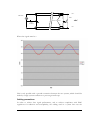
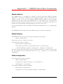
The Xilinx FPGA used on the HERON-IO5 does not have a single clock input, but rather
it can use any one of its pins to provide a clock input. This means you can have many
sources of clocks, each of which can be used inside your FPGA design. You can even
divide these clocks using flip flops, or even multiply using digital clock manager
components.
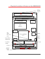
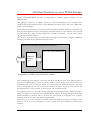
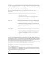
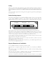
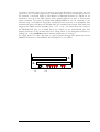
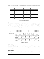
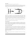
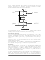
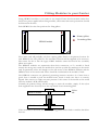
Clock Options
Necessary clocks
OSC1 (100Mhz)
Output FIFO clock
OSC2( -DO only)
feedback
8 Bit Digital I/O
Input FIFO clock
Your FPGA design
feedback
UMI0,1,2&3
ADC Clocks
ADC data Clock
AC Clock Input
DAC Clocks
DAC data Clock
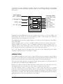
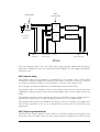
The simplest way to manage your FPGA design is to use just one clock throughout your
design. However the FPGA must drive both of the HERON FIFO clocks, at a frequency
that is suitable for your module carrier (see the documentation for your module carrier for
details of its restrictions). The FPGA must also drive the A/D clocks, and the D/A clocks.
The frequency for these might be limited by the components, or by the needs of your signal
processing. The needs for these clocks can only be determined by looking carefully at the
needs of your system.
The ‘AC CLK’ input can be used as a clock source for the FPGA and/or a clock for the
A/D converters. This 50 Ohm input can be driven with a low level sinusoid, or by logic
levels such as LVTTL. The selection of clock signals for the A/D converters is achieved
with a LVPECL multiplexer, this allows the FPGA or the ‘AC CLK’ input to source the
clock for each or both of the A/D converters. If the ‘AC CLK’ input is selected as the
source for both of the converters then the maximum propagation delay through the active
devices is 965 picoSeconds at 25 degC, and the maximum skew is 100 picoSeconds. It is
recommended that if the ‘AC CLK’ input is used to clock the A/D converters a sinusoid is
used to drive the input as this will give the best jitter performance.
On the HERON-IO5-DO there is a site for a second surface mount user crystal oscillator,
an oscillator is not fitted here as standard build. The OSC2 site is for a 3.3Volt LVDS
oscillator, Golledge type GXO-L71 or equivalent, which allows oscillator frequencies up to
250MHz.
The AD9430 A/D converters used on the HERON-IO5 generate a ‘data clock’ that is
synchronised to the data output from that converter to facilitate registering of the data into
the FPGA, this then becomes a clock input to the FPGA for use with associated logic.
The AD9777 D/A converter used on the HERON-IO5 also generates a ‘data clock’. This
is synchronised to when the DAC expects data on its ports in the operating mode where the
PLL is disabled. If the PLL is enabled then the timing of the data clocked into the D/A is
related to the ‘sample clock’ not to the ‘data clock’ generated by the D/A.
The most difficult case for your FPGA design is to have many clocks from different
sources that are all used in the same design. Then you must carefully manage signals that
11
HUNT ENGINEERING HERON-IO5V USER MANUAL