1
5 PERIPHERAL CIRCUITS AND THEIR OPERATION (Input Ports)
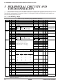
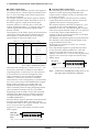
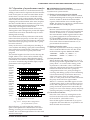
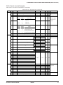
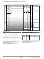
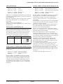
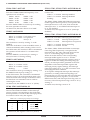
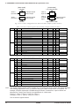
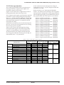
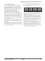
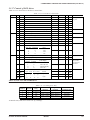
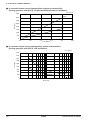
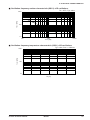
Table 5.5.4.1 Setting the input level check time
CTK02x
1
1
1
1
0
0
0
0
CTK01x
1
1
0
0
1
1
0
0
CTK00x Check time
1
4/fOSC3
0
2/fOSC3
1
1/fOSC3
0
4096/fOSC1
1
2048/fOSC1
0
512/fOSC1
1
128/fOSC1
0
None
(∗)
(2 µs)
(1 µs)
(0.5 µs)
(128 ms)
(64 ms)
(16 ms)
(4 ms)
–
∗: When OSC1 = 32 kHz, OSC3 = 2 MHz
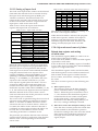
Check time setup register
CTK00L–CTK02L
K00
Input port
K00D
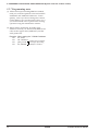
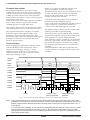
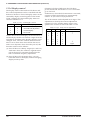
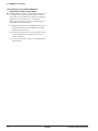
Notes: • Be sure to disable interrupts before
changing the contents of the CTK0x
register. Unnecessary interrupts may
occur if the register is changed when the
corresponding input port interrupts have
been enabled by the interrupt enable
register EK0x.
• The chattering-eliminate check time
means the maximum pulse width that can
be eliminated. The valid interrupt input
needs a pulse width of the set check time
(minimum) to twice that of the check time
(maximum).
• The internal signal may oscillate if the rise /
fall time of the input signal is too long
because the input signal level transition to
the threshold level duration of time is too
long. This causes the input interrupt to
malfunction, therefore setup the input signal
so that the rise/fall time is 25 nsec or less.
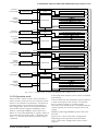
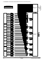
Address
Divider
Chattering-eliminate
circuit
Input comparison
register KCP00
Interrupt factor
flag FK00
Address
Divider
fOSC1
OSC1
oscillation circuit
fOSC3
OSC3
oscillation circuit
Address
Interrupt enable
register EK00
Data bus
Address
K01
K02
K03
Check time setup register
CTK00H–CTK02H
K04
Input port
K04D
Address
Interrupt
request
Chattering-eliminate
circuit
Input comparison
register KCP04
Address
Interrupt
priority level
judgement
circuit
Interrupt factor
flag FK04
Address
Interrupt enable
register EK04
Address
K05
K06
K07
Interrupt
priority
register
PK00, PK01
Address
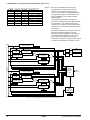
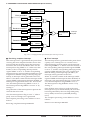
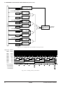
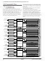
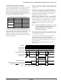
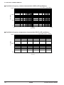
Fig. 5.5.4.1 Configuration of input interrupt circuit
46
EPSON
S1C88650 TECHNICAL MANUAL