1
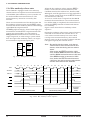
CMOS 8-BIT SINGLE CHIP MICROCOMPUTER
S1C88650
Technical Manual
S1C88650 Technical Hardware
NOTICE
No part of this material may be reproduced or duplicated in any form or by any means without the written permission of Seiko
Epson. Seiko Epson reserves the right to make changes to this material without notice. Seiko Epson does not assume any
liability of any kind arising out of any inaccuracies contained in this material or due to its application or use in any product or
circuit and, further, there is no representation that this material is applicable to products requiring high level reliability, such
as medical products. Moreover, no license to any intellectual property rights is granted by implication or otherwise, and there
is no representation or warranty that anything made in accordance with this material will be free from any patent or copyright
infringement of a third party. This material or portions thereof may contain technology or the subject relating to strategic
products under the control of the Foreign Exchange and Foreign Trade Law of Japan and may require an export license from
the Ministry of International Trade and Industry or other approval from another government agency.
© SEIKO EPSON CORPORATION 2004, All rights reserved.
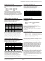
Configuration of product number
Devices
S1
C
88104
F
0A01
00
Packing specifications
00 : Besides tape & reel
0A : TCP BL
2 directions
0B : Tape & reel BACK
0C : TCP BR
2 directions
0D : TCP BT
2 directions
0E : TCP BD
2 directions
0F : Tape & reel FRONT
0G : TCP BT
4 directions
0H : TCP BD
4 directions
0J : TCP SL
2 directions
0K : TCP SR
2 directions
0L : Tape & reel LEFT
0M: TCP ST
2 directions
0N : TCP SD
2 directions
0P : TCP ST
4 directions
0Q : TCP SD
4 directions
0R : Tape & reel RIGHT
99 : Specs not fixed
Specification
Package
D: die form; F: QFP
Model number
Model name
C: microcomputer, digital products
Product classification
S1: semiconductor
Development tools
S5U1
C
88348
D1
1
00
Packing specifications
00: standard packing
Version
1: Version 1
Tool type
Hx : ICE
Ex : EVA board
Px : Peripheral board
Wx: Flash ROM writer for the microcomputer
Xx : ROM writer peripheral board
Cx : C compiler package
Ax : Assembler package
Dx : Utility tool by the model
Qx : Soft simulator
Corresponding model number
88348: for S1C88348
Tool classification
C: microcomputer use
Product classification
S5U1: development tool for semiconductor products
S1C88 Family
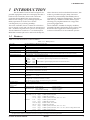
CONTENTS
Contents
1
INTRODUCTION .............................................................................................. 1
1.1
1.2
1.3
Features .............................................................................................................................1
Block Diagram ...................................................................................................................2
Pins ....................................................................................................................................3
1.3.1 Pin layout diagram ................................................................................................................... 3
1.3.2 Pin description ......................................................................................................................... 4
1.4
2
POWER SUPPLY ............................................................................................... 7
2.1
2.2
3
Mask Option .......................................................................................................................5
Operating Voltage ..............................................................................................................7
Internal Power Supply Circuit ...........................................................................................7
CPU AND BUS CONFIGURATION ................................................................ 8
3.1
3.2
CPU ...................................................................................................................................8
Internal Memory ................................................................................................................ 8
3.2.1 Program ROM .......................................................................................................................... 8
3.2.2 RAM .......................................................................................................................................... 8
3.2.3 I/O memory ............................................................................................................................... 8
3.2.4 Display memory ........................................................................................................................ 8
3.2.5 Kanji font ROM ........................................................................................................................ 8
3.3
3.4
3.5
Exception Processing Vectors ...........................................................................................9
CC (Customized Condition Flag) ......................................................................................9
Chip Mode ..........................................................................................................................9
3.5.1 MCU mode and MPU mode ..................................................................................................... 9
3.5.2 Bus mode ................................................................................................................................. 10
3.5.3 CPU mode ............................................................................................................................... 11
3.6
External Bus ......................................................................................................................11
3.6.1 Data bus .................................................................................................................................. 11
3.6.2 Address bus ............................................................................................................................. 12
3.6.3 Read (RD)/write (WR) signals ................................................................................................. 12
3.6.4 Chip enable (CE) signal .......................................................................................................... 12
3.6.5 WAIT control ........................................................................................................................... 13
3.6.6 Bus authority release state ...................................................................................................... 14
4
INITIAL RESET ............................................................................................... 15
4.1
Initial Reset Factors ..........................................................................................................15
4.1.1 RESET terminal ....................................................................................................................... 15
4.1.2 Simultaneous LOW level input at input port terminals K00–K03 ........................................... 16
4.1.3 Initial reset sequence ............................................................................................................... 16
4.2
5
Initial Settings After Initial Reset ......................................................................................17
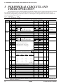
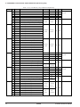
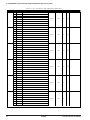
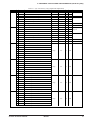
PERIPHERAL CIRCUITS AND THEIR OPERATION ................................ 18
5.1
5.2
I/O Memory Map .............................................................................................................. 18
System Controller and Bus Control ..................................................................................34
5.2.1 Bus mode and CPU mode settings .......................................................................................... 34
5.2.2 Address decoder (CE output) settings ..................................................................................... 34
5.2.3 WAIT state settings .................................................................................................................. 35
5.2.4 Setting the bus authority release request signal ...................................................................... 35
5.2.5 Stack page setting .................................................................................................................... 35
5.2.6 Control of system controller .................................................................................................... 36
5.2.7 Programming notes ................................................................................................................. 38
S1C88650 TECHNICAL MANUAL
EPSON
i
CONTENTS
5.3
Watchdog Timer ................................................................................................................39
5.3.1 Configuration of watchdog timer ............................................................................................ 39
5.3.2 Interrupt function .................................................................................................................... 39
5.3.3 Control of watchdog timer ...................................................................................................... 40
5.3.4 Programming notes ................................................................................................................. 40
5.4
Oscillation Circuits ...........................................................................................................41
5.4.1 Configuration of oscillation circuits ....................................................................................... 41
5.4.2 Mask option ............................................................................................................................. 41
5.4.3 OSC1 oscillation circuit .......................................................................................................... 41
5.4.4 OSC3 oscillation circuit .......................................................................................................... 42
5.4.5 Switching the CPU clocks ....................................................................................................... 42
5.4.6 Control of oscillation circuit ................................................................................................... 43
5.4.7 Programming notes ................................................................................................................. 43
5.5
Input Ports (K ports) .........................................................................................................44
5.5.1 Configuration of input ports .................................................................................................... 44
5.5.2 Mask option ............................................................................................................................. 44
5.5.3 Pull-up control ........................................................................................................................ 45
5.5.4 Interrupt function and input comparison register ................................................................... 45
5.5.5 Control of input ports .............................................................................................................. 47
5.5.6 Programming notes ................................................................................................................. 50
5.6
Output Ports (R ports) ......................................................................................................51
5.6.1 Configuration of output ports .................................................................................................. 51
5.6.2 High impedance control .......................................................................................................... 51
5.6.3 DC output ................................................................................................................................ 51
5.6.4 Control of output ports ............................................................................................................ 52
5.7
I/O Ports (P ports) ............................................................................................................54
5.7.1 Configuration of I/O ports ....................................................................................................... 54
5.7.2 Mask option ............................................................................................................................. 54
5.7.3 I/O control registers and I/O mode ......................................................................................... 54
5.7.4 Pull-up control ........................................................................................................................ 55
5.7.5 Special output .......................................................................................................................... 55
5.7.6 Control of I/O ports ................................................................................................................. 57
5.7.7 Programming notes ................................................................................................................. 60
5.8
Serial Interface .................................................................................................................61
5.8.1 Configuration of serial interface ............................................................................................. 61
5.8.2 Switching of terminal functions ............................................................................................... 61
5.8.3 Transfer modes ........................................................................................................................ 62
5.8.4 Clock source ............................................................................................................................ 63
5.8.5 Transmit-receive control ......................................................................................................... 64
5.8.6 Operation of clock synchronous transfer ................................................................................ 65
5.8.7 Operation of asynchronous transfer ....................................................................................... 69
5.8.8 Interrupt function .................................................................................................................... 73
5.8.9 Control of serial interface ....................................................................................................... 75
5.8.10 Programming notes ............................................................................................................... 80
5.9
Clock Timer .......................................................................................................................81
5.9.1 Configuration of clock timer ................................................................................................... 81
5.9.2 Interrupt function .................................................................................................................... 81
5.9.3 Control of clock timer ............................................................................................................. 83
5.9.4 Programming notes ................................................................................................................. 85
5.10
Programmable Timer ........................................................................................................86
5.10.1 Configuration of programmable timer .................................................................................. 86
5.10.2 Operation mode ..................................................................................................................... 87
5.10.3 Setting of input clock ............................................................................................................. 89
5.10.4 Operation and control of timer ............................................................................................. 89
5.10.5 Interrupt function .................................................................................................................. 91
5.10.6 Setting of TOUT output ......................................................................................................... 93
5.10.7 Transfer rate setting of serial interface ................................................................................. 94
ii
EPSON
S1C88650 TECHNICAL MANUAL
CONTENTS
5.10.8 Setting frame frequency for LCD driver ............................................................................... 94
5.10.9 Control of programmable timer ............................................................................................ 95
5.10.10 Programming notes ............................................................................................................ 107
5.11
LCD Driver ......................................................................................................................108
5.11.1 Configuration of LCD driver ................................................................................................ 108
5.11.2 LCD power supply ................................................................................................................ 108
5.11.3 Frame frequency .................................................................................................................. 109
5.11.4 Switching drive duty ............................................................................................................. 109
5.11.5 Display memory .................................................................................................................... 113
5.11.6 Display control ..................................................................................................................... 120
5.11.7 Control of LCD driver .......................................................................................................... 121
5.11.8 Programming notes .............................................................................................................. 123
5.12
Supply Voltage Detection (SVD) Circuit .........................................................................124
5.12.1 Configuration of SVD circuit ............................................................................................... 124
5.12.2 SVD operation ...................................................................................................................... 124
5.12.3 Control of SVD circuit .......................................................................................................... 125
5.12.4 Programming notes .............................................................................................................. 125
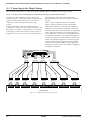
5.13
Heavy Load Protection Function .....................................................................................126
5.13.1 Outline of heavy load protection function ............................................................................ 126
5.13.2 Control of heavy load protection function ........................................................................... 126
5.13.3 Programming note ................................................................................................................ 126
5.14
Interrupt and Standby Status ...........................................................................................127
5.14.1 Interrupt generation conditions ........................................................................................... 127
5.14.2 Interrupt factor flag .............................................................................................................. 129
5.14.3 Interrupt enable register ...................................................................................................... 130
5.14.4 Interrupt priority register and interrupt priority level ......................................................... 131
5.14.5 Exception processing vectors ............................................................................................... 132
5.14.6 Control of interrupt .............................................................................................................. 133
5.14.7 Programming notes .............................................................................................................. 135
6
SUMMARY OF NOTES .................................................................................. 136
6.1
6.2
Notes for Low Current Consumption ...............................................................................136
Precautions on Mounting .................................................................................................137
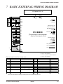
7
BASIC EXTERNAL WIRING DIAGRAM ..................................................... 139
8
ELECTRICAL CHARACTERISTICS ............................................................ 140
8.1
8.2
8.3
8.4
8.5
8.6
8.7
8.8
9
PACKAGE ........................................................................................................ 159
9.1
9.2
10
Absolute Maximum Rating ...............................................................................................140
Recommended Operating Conditions ..............................................................................140
DC Characteristics ..........................................................................................................141
Analog Circuit Characteristics ........................................................................................142
Power Current Consumption ...........................................................................................143
AC Characteristics ...........................................................................................................144
Oscillation Characteristics ..............................................................................................149
Characteristics Curves (reference value) ........................................................................150
Plastic Package ................................................................................................................159
Ceramic Package for Test Samples .................................................................................160
PAD LAYOUT .................................................................................................. 161
10.1
10.2
Diagram of Pad Layout ...................................................................................................161
Pad Coordinates ..............................................................................................................162
S1C88650 TECHNICAL MANUAL
EPSON
iii
CONTENTS
APPENDIX A S5U1C88000P1&S5U1C88649P2 MANUAL
(Peripheral Circuit Board for S1C88650) ...................................... 163
A.1
A.2
Names and Functions of Each Part .................................................................................163
Precautions ......................................................................................................................165
A.2.1 Precaution for operation ....................................................................................................... 165
A.2.2 Differences from actual IC .................................................................................................... 165
A.3
A.4
Connecting to the Target System .....................................................................................168
Product Specifications .....................................................................................................171
APPENDIX B USING KANJI FONT ..................................................................... 172
iv
EPSON
S1C88650 TECHNICAL MANUAL
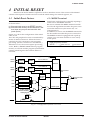
1 INTRODUCTION
1 INTRODUCTION
The S1C88650 is an 8-bit microcomputer for
portable equipment with an LCD display that has a
built-in LCD controller/driver and a character
generator (kanji) ROM. This microcomputer
features low-voltage (1.8 V) and high-speed (8.2
MHz) operations as well as low-current
consumption (2.5 µA during standby).
The LCD controller/driver contains an LCD drive
power supply circuit and can drive an maximum of
126 × 32-dot LCD panel in low-power consumption.
The S1C88650 has a built-in 11 × 12-dot kanji font
ROM that contains JIS level-1 and level-2 kanji sets,
other characters and user-defined characters, this
makes it possible to display kanji characters
without any external kanji font ROM (refer to
Appendix B, "USING KANJI FONT"). This 8-bit
CPU has up to 16MB accessible address space
allowing easy implementation of a large data
processing application.
The S1C88650 is suitable for display modules,
portable CD/MD, solid audio players, PDA, data
bank and other applications that required an
exclusive LCD driver in conventional systems.
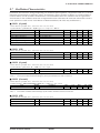
1.1 Features
Table 1.1.1 lists the features of the S1C88650.
Table 1.1.1 Main features
Core CPU
S1C88 (MODEL3) CMOS 8-bit core CPU
Crystal oscillation circuit/ceramic oscillation circuit 8.2 MHz (Max.), or CR oscillation circuit 2.2 MHz (Max.)
Sub (OSC1) oscillation circuit Crystal oscillation circuit 32.768 kHz (Typ.), or CR oscillation circuit 200 kHz (Max.)
Instruction set
608 types (usable for multiplication and division instructions)
Min. instruction execution time 0.244 µsec/8.2 MHz (2 clock)
Internal ROM capacity
48K bytes/program ROM
896K bytes/kanji font ROM (can be used for a program and data ROM when no font data is stored.)
Internal RAM capacity
8K bytes/RAM 768 bytes/display memory
Bus line
Address bus: 20 bits (also usable as general output ports when not used for the bus)
Data bus:
8 bits
(also usable as general I/O ports when not used for the bus)
CE signal:
3 bits
WR signal: 1 bit
(also usable as general output ports when not used for the bus)
RD signal:
1 bit
Input port
8 bits (4 bits can be used as the source clock inputs for PWM timers and 1 bit as a bus request signal input)
(1 bit can be configured for the bus acknowledge signal output)
Output port
0–3 bits (when the external bus is used)
Main (OSC3) oscillation circuit
I/O port
Serial interface
Timer
LCD driver
Watchdog timer
Supply voltage detection
(SVD) circuit
Interrupt
Supply voltage
Current consumption
26 bits (when the external bus is not used)
(shard with serial interface, FOUT and TOUT terminals)
8 bits (when the external bus is used)
16 bits (when the external bus is not used)
1 ch (optional clock synchronous system or asynchronous system)
Programmable timer: 16 bits (8 bits × 2) 4 ch (with PWM function)
1 ch
Clock timer:
Dot matrix type (supports 16 × 16/5 × 8 or 12 × 12 dot font)
126 segments × 32, 16 or 8 commons (1/5 bias)
Built-in LCD power supply circuit (booster type, 5 potentials)
Built-in (1–8 second cycles)
13 value programmable (1.8–2.7 V)
External interrupt: Input interrupt
Internal interrupt: Timer interrupt
Serial interface interrupt
1.8–3.6 V
SLEEP mode: 1 µA
HALT mode: 2.5 µA
(Typ.)
(Typ.)
32 kHz crystal, LCD OFF
10 µA
7.6 µA
(Typ.)
(Typ.)
32 kHz CR, LCD OFF
32 kHz crystal, LCD ON*, VDD = 2.5–3.6 V
9 µA
15 µA
1700 µA
600 µA
14 µA
(Typ.)
(Typ.)
(Typ.)
(Typ.)
(Typ.)
32 kHz crystal, LCD OFF
32 kHz CR, LCD OFF
8 MHz ceramic, LCD OFF
2 MHz CR, LCD OFF
32 kHz crystal, LCD ON*, VDD = 2.5–3.6 V
19 µA
(Typ.)
32 kHz crystal, LCD ON*, VDD = 1.8–2.5 V, Power voltage booster ON
Run state:
Supply form
1 system (8 types)
2 systems (16 types)
1 system (3 types)
14 µA
(Typ.)
QFP22-256pin or chip
32 kHz crystal, SVD ON
∗ The current consumption with LCD ON listed above is the value under the conditions of LCDCx = "11 (all on)", LCx = "0FH" and
"No panel load". Current consumption increases according to the display contents and panel load.
S1C88650 TECHNICAL MANUAL
EPSON
1
1 INTRODUCTION
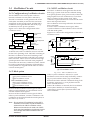
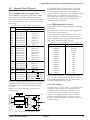
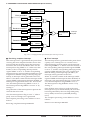
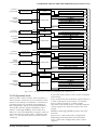
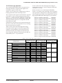
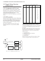
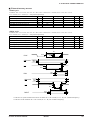
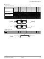
1.2 Block Diagram
Core CPU S1C88
OSC1, 2
Oscillator
Interrupt Controller
System Controller
Input Port
Reset/Test
I/O Port
OSC3, 4
MCU/MPU
BREQ (K03)
BACK (R33)
RESET
TEST
EXCL0–EXCL3 (K04–K07)
TOUT0–TOUT3 (P14, P15)
TOUT2/TOUT3 (P17)
Watchdog Timer
Serial Interface
Programmable Timer
/Event Counter
External
Memory Interface
Clock Timer
Output Port
VDD
VD2
P10 (SIN)
P11 (SOUT)
P12 (SCLK)
P13 (SRDY)
P14 (TOUT0/TOUT1)
P15 (TOUT2/TOUT3)
P16 (FOUT)
P17 (TOUT2/TOUT3)
P00–P07 (D0–D7)
R00–R07, R10–R17, R20–R23
(A0–A7, A8–A15, A16–A19)
R24, R25 (RD, WR)
R30–R32 (CE0–CE2)
R33 (BACK)
SEG0–SEG125
LCD Driver
VSS
VD1
K00–K02
K03 (BREQ)
K04–K07
COM0–COM31
Power Generator
VC1–VC5
Supply Voltage Detector
CA–CG
RAM
8K bytes
ROM
48K bytes+896K bytes
Fig. 1.2.1 S1C88650 block diagram
2
EPSON
S1C88650 TECHNICAL MANUAL
1 INTRODUCTION
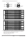
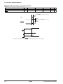
1.3 Pins
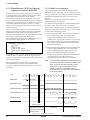
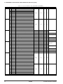
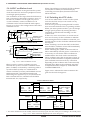
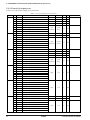
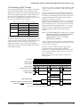
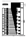
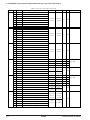
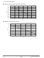
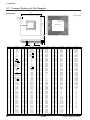
1.3.1 Pin layout diagram
QFP22-256pin
192
129
128
193
INDEX
65
256
1
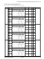
Pin No.
1
2
3
4
5
6
7
8
9
10
11
12
13
14
15
16
17
18
19
20
21
22
23
24
25
26
27
28
29
30
31
32
33
34
35
36
37
38
39
40
41
42
43
44
45
46
47
48
49
50
51
52
Pin name
N.C.
N.C.
TEST
SEG39
SEG40
SEG41
SEG42
SEG43
SEG44
SEG45
SEG46
SEG47
SEG48
SEG49
SEG50
SEG51
SEG52
SEG53
SEG54
SEG55
SEG56
SEG57
SEG58
SEG59
SEG60
SEG61
SEG62
SEG63
SEG64
SEG65
SEG66
SEG67
SEG68
SEG69
SEG70
SEG71
SEG72
SEG73
SEG74
SEG75
SEG76
SEG77
SEG78
SEG79
SEG80
SEG81
SEG82
SEG83
SEG84
SEG85
SEG86
SEG87
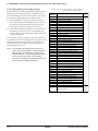
Pin No.
53
54
55
56
57
58
59
60
61
62
63
64
65
66
67
68
69
70
71
72
73
74
75
76
77
78
79
80
81
82
83
84
85
86
87
88
89
90
91
92
93
94
95
96
97
98
99
100
101
102
103
104
Pin name
SEG88
SEG89
SEG90
SEG91
SEG92
SEG93
SEG94
SEG95
SEG96
N.C.
N.C.
N.C.
N.C.
N.C.
VSS
SEG97
SEG98
SEG99
SEG100
SEG101
SEG102
SEG103
SEG104
SEG105
SEG106
SEG107
SEG108
SEG109
SEG110
SEG111
SEG112
SEG113
SEG114
SEG115
SEG116
SEG117
SEG118
SEG119
SEG120
SEG121
SEG122
SEG123
SEG124
SEG125
COM31
COM30
COM29
COM28
COM27
COM26
COM25
COM24
64
Pin No.
Pin name
Pin No.
105
COM23
157
106
COM22
158
107
COM21
159
160
108
COM20
109
COM19
161
162
110
COM18
163
111
COM17
112
COM16
164
113
VD2
165
CG
114
166
CF
167
115
CE
116
168
CD
117
169
CC
118
170
CB
119
171
CA
172
120
VC5
121
173
174
122
VC4
VC3
175
123
124
VC2
176
125
177
VC1
126
178
N.C.
179
127
N.C.
180
128
N.C.
129
181
N.C.
130
182
N.C.
131
183
VDD
184
132
OSC3
133
OSC4
185
VSS
186
134
187
135
VD1
136
OSC1
188
137
OSC2
189
138
TEST
190
RESET
191
139
140
MCU/MPU
192
141
K07/EXCL3
193
K06/EXCL2
194
142
143
K05/EXCL1
195
144
K04/EXCL0
196
145
K03/BREQ
197
146
K02
198
147
K01
199
148
K00
200
149 P17/TOUT2/TOUT3 201
150
P16/FOUT
202
151 P15/TOUT2/TOUT3 203
152 P14/TOUT0/TOUT1 204
153
P13/SRDY
205
154
P12/SCLK
206
155
P11/SOUT
207
156
P10/SIN
208
Pin name
P07/D7
P06/D6
P05/D5
P04/D4
P03/D3
P02/D2
P01/D1
P00/D0
R00/A0
R01/A1
R02/A2
R03/A3
R04/A4
R05/A5
R06/A6
R07/A7
R10/A8
R11/A9
R12/A10
R13/A11
R14/A12
R15/A13
R16/A14
R17/A15
R20/A16
R21/A17
R22/A18
R23/A19
R24/RD
R25/WR
R30/CE0
R31/CE1
VDD
N.C.
N.C.
N.C.
N.C.
N.C.
VSS
R32/CE2
R33/BACK
COM0
COM1
COM2
COM3
COM4
COM5
COM6
COM7
COM8
COM9
COM10
Pin No.
209
210
211
212
213
214
215
216
217
218
219
220
221
222
223
224
225
226
227
228
229
230
231
232
233
234
235
236
237
238
239
240
241
242
243
244
245
246
247
248
249
250
251
252
253
254
255
256
–
–
–
–
Pin name
COM11
COM12
COM13
COM14
COM15
SEG0
SEG1
SEG2
SEG3
SEG4
SEG5
SEG6
SEG7
SEG8
SEG9
SEG10
SEG11
SEG12
SEG13
SEG14
SEG15
SEG16
SEG17
SEG18
SEG19
SEG20
SEG21
SEG22
SEG23
SEG24
SEG25
SEG26
SEG27
SEG28
SEG29
SEG30
SEG31
SEG32
SEG33
SEG34
SEG35
SEG36
SEG37
SEG38
VSS
N.C.
N.C.
N.C.
–
–
–
–
Fig. 1.3.1.1 S1C88650 pin layout
S1C88650 TECHNICAL MANUAL
EPSON
3
1 INTRODUCTION
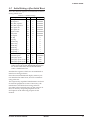
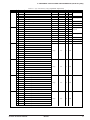
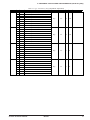
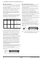
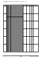
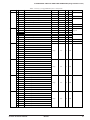
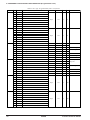
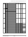
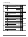
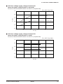
1.3.2 Pin description
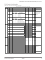
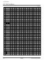
Table 1.3.2.1 S1C88650 pin description
Pin No.
In/Out
Function
VDD
131, 189
–
Power supply (+) terminal
67, 134, 195, 253
–
Power supply (GND) terminal
VSS
135
–
Internal logic system and oscillation system voltage regulator output terminals
VD1
113
–
LCD circuit power voltage booster output terminal
VD2
VC1–VC5
125–121
–
LCD drive voltage output terminals
120–114
–
LCD and power voltage booster capacitor connection terminals
CA–CG
136
I
OSC1 oscillation input terminal (select crystal/CR oscillation by mask option)
OSC1
137
O
OSC1 oscillation output terminal
OSC2
132
I
OSC3 oscillation input terminal (select crystal/ceramic/CR oscillation by mask option)
OSC3
133
O
OSC3 oscillation output terminal
OSC4
140
I
MCU/MPU mode setup terminal
MCU/MPU
148–146
I
Input terminals (K00–K02)
K00–K02
145
I
Input terminal (K03) or bus request signal input terminal (BREQ)
K03/BREQ
144
I
Input terminal (K04) or programmable timer external clock input terminal (EXCL0)
K04/EXCL0
143
I
Input terminal (K05) or programmable timer external clock input terminal (EXCL1)
K05/EXCL1
142
I
Input terminal (K06) or programmable timer external clock input terminal (EXCL2)
K06/EXCL2
141
I
Input terminal (K07) or programmable timer external clock input terminal (EXCL3)
K07/EXCL3
165–172
O
Output terminals (R00–R07) or address bus (A0–A7)
R00–R07/A0–A7
173–180
O
Output terminals (R10–R17) or address bus (A8–A15)
R10–R17/A8–A15
181–184
O
Output terminals (R20–R23) or address bus (A16–A19)
R20–R23/A16–A19
185
O
Output terminal (R24) or read signal output terminal (RD)
R24/RD
186
O
Output terminal (R25) or write signal output terminal (WR)
R25/WR
187, 188, 196
O
Output terminals (R30–R32) or chip enable signal output terminals (CE0–CE2)
R30–R32/CE0–CE2
197
O
Output terminal (R33) or bus acknowledge signal output terminal (BACK)
R33 (BACK)
164–157
I/O
I/O terminals (P00–P07) or data bus (D0–D7)
P00–P07/D0–D7
156
I/O
I/O terminal (P10) or serial I/F data input terminal (SIN)
P10/SIN
155
I/O
I/O terminal (P11) or serial I/F data output terminal (SOUT)
P11/SOUT
154
I/O
I/O terminal (P12) or serial I/F clock I/O terminal (SCLK)
P12/SCLK
153
I/O
I/O terminal (P13) or serial I/F ready signal output terminal (SRDY)
P13/SRDY
152
I/O
I/O terminal (P14)
P14/TOUT0/TOUT1
or programmable timer underflow signal output terminal (TOUT0/TOUT1)
151
I/O
I/O terminal (P15)
P15/TOUT2/TOUT3
or programmable timer underflow signal output terminal (TOUT2/TOUT3)
150
I/O
I/O terminal (P16) or clock output terminal (FOUT)
P16/FOUT
149
I/O
I/O terminal (P17)
P17/TOUT2/TOUT3
or programmable timer underflow inverted signal output terminal (TOUT2/TOUT3)
198–213, 112–97
O
LCD common output terminals
COM0–COM31
214–252, 4–61,
O
LCD segment output terminals
SEG0–SEG125
68–96
139
I
Initial reset input terminal
RESET
138
I
Test input terminal
TEST
3
–
Test terminal (open during normal operation)
TEST
Pin name
4
EPSON
S1C88650 TECHNICAL MANUAL
1 INTRODUCTION
1.4 Mask Option
Mask options shown below are provided for the
S1C88650.
Several hardware specifications are prepared in
each mask option, and one of them can be selected
according to the application. Multiple specifications
are available in each option item as indicated in the
Option List.
Select the specifications that meet the target system
and check the appropriate box.
The option selection is done interactively on the
screen during function option generator winfog
execution, using this option list as reference. Mask
pattern of the IC is finally generated based on the
data created by the winfog. Refer to the
"S5U1C88000C Manual II" for details on the winfog.
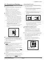
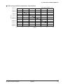
PERIPHERAL CIRCUIT BOARD option list
The following shows the options for configuring the Peripheral Circuit Board (S5U1C88000P1 with
S5U1C88649P2) installed in the ICE (S5U1C88000H5). The selections do not affect the IC's mask option.
A OSC1 SYSTEM CLOCK
■ 1. Internal Clock
■ 2. User Clock
When User Clock is selected, input a clock to the OSC1
terminal. When Internal Clock is selected, the clock
frequency is changed according to the oscillation circuit
selected by the IC's mask option.
B OSC3 SYSTEM CLOCK
■ 1. Internal Clock
■ 2. User Clock
When User Clock is selected, input a clock to the OSC3
terminal. When Internal Clock is selected, the clock
frequency is changed according to the oscillation circuit
selected by the IC's mask option.
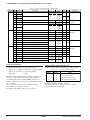
S1C88650 mask option list
The following shows the option list for generating the IC's mask pattern. Note that the Peripheral Circuit
Board installed in the ICE does not support some options.
1 OSC1 SYSTEM CLOCK
■ 1. Crystal
■ 2. CR
The specification of the OSC1 oscillation circuit can be
selected from among two types: "Crystal oscillation" and
"CR oscillation". Refer to Section 5.4.3, "OSC1 oscillation
circuit", for details.
2 OSC3 SYSTEM CLOCK
■ 1. Crystal
■ 2. Ceramic
■ 3. CR
The specification of the OSC3 oscillation circuit can be
selected from among three types: "Crystal oscillation",
"Ceramic oscillation" and "CR oscillation". Refer to
Section 5.4.4, "OSC3 oscillation circuit", for details.
3 MULTIPLE KEY ENTRY RESET
• Combination .. ■
■
■
■
This mask option can select whether the multiple key
entry reset function is used or not. When the function is
used, a combination of the input ports (K00–K03), which
are connected to the keys, can be selected. Refer to
Section 4.1.2, "Simultaneous LOW level input at input
port terminals K00–K03", for details.
1. Not Use
2. Use K00, K01
3. Use K00, K01, K02
4. Use K00, K01, K02, K03
4 INPUT PORT PULL UP RESISTOR
• K00 ................... ■
• K01 ................... ■
• K02 ................... ■
• K03 ................... ■
• K04 ................... ■
• K05 ................... ■
• K06 ................... ■
• K07 ...................
■
______
• MCU/MPU
.... ■
________
• RESET ............. ■
1. With Resistor
1. With Resistor
1. With Resistor
1. With Resistor
1. With Resistor
1. With Resistor
1. With Resistor
1. With Resistor
1. With Resistor
1. With Resistor
S1C88650 TECHNICAL MANUAL
■
■
■
■
■
■
■
■
■
■
2. Gate Direct
2. Gate Direct
2. Gate Direct
2. Gate Direct
2. Gate Direct
2. Gate Direct
2. Gate Direct
2. Gate Direct
2. Gate Direct
2. Gate Direct
This mask option can select whether the pull-up resistor
for the input (K) port terminal is used or not. It is
possible to select for each bit of the input ports. Refer to
Section 5.5, "Input Ports (K ports)", for details.
Furthermore,
______ a pull-up
________option is also provided for the
MCU/MPU and RESET terminals.
EPSON
5
1 INTRODUCTION
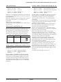
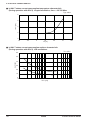
5 I/O PORT PULL UP RESISTOR
• P00 ......... ■
• P01 ......... ■
• P02 ......... ■
• P03 ......... ■
• P04 ......... ■
• P05 ......... ■
• P06 ......... ■
• P07 ......... ■
• P10 ......... ■
• P11 ......... ■
• P12 ......... ■
• P13 ......... ■
• P14 ......... ■
• P15 ......... ■
• P16 ......... ■
• P17 ......... ■
1. With Resistor
1. With Resistor
1. With Resistor
1. With Resistor
1. With Resistor
1. With Resistor
1. With Resistor
1. With Resistor
1. With Resistor
1. With Resistor
1. With Resistor
1. With Resistor
1. With Resistor
1. With Resistor
1. With Resistor
1. With Resistor
■
■
■
■
■
■
■
■
■
■
■
■
■
■
■
■
2. Gate Direct
2. Gate Direct
2. Gate Direct
2. Gate Direct
2. Gate Direct
2. Gate Direct
2. Gate Direct
2. Gate Direct
2. Gate Direct
2. Gate Direct
2. Gate Direct
2. Gate Direct
2. Gate Direct
2. Gate Direct
2. Gate Direct
2. Gate Direct
This mask option can select whether the pull-up resistor
for the I/O port terminal (it works during input mode) is
used or not. It is possible to select for each bit of the I/O
ports. Refer to Section 5.7, "I/O Ports (P ports)", for
details.
■
■
■
■
■
■
■
■
2. CMOS Schmitt
2. CMOS Schmitt
2. CMOS Schmitt
2. CMOS Schmitt
2. CMOS Schmitt
2. CMOS Schmitt
2. CMOS Schmitt
2. CMOS Schmitt
This mask option can select the interface level of the
input (K) port from either the CMOS level or CMOS
Schmitt level. It is possible to select for each bit of the
input ports. Refer to Section 5.5, "Input Ports (K ports)",
for details.
The input port on the ICE (with the Peripheral Circuit
Board installed) is fixed to the CMOS level interface
regardless of this option selection.
■
■
■
■
■
■
■
■
2. CMOS Schmitt
2. CMOS Schmitt
2. CMOS Schmitt
2. CMOS Schmitt
2. CMOS Schmitt
2. CMOS Schmitt
2. CMOS Schmitt
2. CMOS Schmitt
This mask option can select the interface level of the I/O
(P) port from either the CMOS level or CMOS Schmitt
level. It is possible to select for each bit of the I/O ports.
Refer to Section 5.7, "I/O Ports (P ports)", for details.
The input port on the ICE (with the Peripheral Circuit
Board installed) is fixed to the CMOS level interface
regardless of this option selection.
6 INPUT PORT INPUT I/F LEVEL
• K00 ......... ■
• K01 ......... ■
• K02 ......... ■
• K03 ......... ■
• K04 ......... ■
• K05 ......... ■
• K06 ......... ■
• K07 ......... ■
1. CMOS Level
1. CMOS Level
1. CMOS Level
1. CMOS Level
1. CMOS Level
1. CMOS Level
1. CMOS Level
1. CMOS Level
7 I/O PORT INPUT I/F LEVEL
• P10 ......... ■
• P11 ......... ■
• P12 ......... ■
• P13 ......... ■
• P14 ......... ■
• P15 ......... ■
• P16 ......... ■
• P17 ......... ■
1. CMOS Level
1. CMOS Level
1. CMOS Level
1. CMOS Level
1. CMOS Level
1. CMOS Level
1. CMOS Level
1. CMOS Level
______
8 WATCHDOG TIMER NMI GENERATION CYCLE
■ 1. 32768/fOSC1
(0.75–1-sec cycle when fOSC1 = 32 kHz)
■ 2. 65536/fOSC1
(1.5–2-sec cycle when fOSC1 = 32 kHz)
■ 3. 131072/fOSC1
(3–4-sec cycle when fOSC1 = 32 kHz)
■ 4. 262144/fOSC1
(6–8-sec cycle when fOSC1 = 32 kHz)
6
______
This mask option can select the NMI generation cycle of
the watchdog timer. Refer to Section 5.3.1, "Configuration
of watchdog timer", for details.
EPSON
S1C88650 TECHNICAL MANUAL
2 POWER SUPPLY
2 POWER SUPPLY
In this section, we will explain the operating voltage and the configuration of the internal power
supply circuit of the S1C88650.
Either <VDD> or <VD2> can be selected as the
power source for the LCD system voltage regulator
according to the <VDD> power supply voltage
level.
2.1 Operating Voltage
The S1C88650 operating power voltage is as
follows:
1.8 V to 3.6 V
Table 2.2.2 Power source for LCD system
voltage regulator
2.2 Internal Power Supply Circuit
The S1C88650 incorporates the power supply
circuit shown in Figure 2.2.1. When voltage within
the range described above is supplied to VDD (+)
and VSS (GND), all the voltages needed for the
internal circuit are generated internally in the IC.
Roughly speaking, the power supply circuit is
divided into three sections.
Table 2.2.1 Power supply circuit
Circuit
Oscillation circuits,
Internal circuits
LCD system voltage
regulator
LCD driver
Power supply circuit Output voltage
Internal logic
VD1
voltage regulator
Power voltage
VDD or VD2
booster
LCD system voltage VC1–VC5
regulator
The internal logic voltage regulator generates the
operating voltage <VD1> for driving the internal
logic circuits and the oscillation circuit.
The VD1 voltage value is fixed at 1.8 V (Typ.).
Supply voltage
VDD
1.8–2.5 V
2.5–3.6 V
The VD2 voltage is about double the VDD voltage
level. Refer to Chapter 8, "ELECTRICAL
CHARACTERISTICS", for details.
The LCD system voltage regulator generates the 1/
5-bias LCD drive voltages <VC1>, <VC2>, <VC3>,
<VC4> and <VC5>. See Chapter 8, "ELECTRICAL
CHARACTERISTICS" for the voltage values.
In the S1C88650, the LCD drive voltage is supplied
to the built-in LCD driver which drives the LCD
panel connected to the SEG and COM terminals.
Notes: • Under no circumstances should VD1,VD2,
VC1, VC2, VC3, VC4 and VC5, terminal
output be used to drive external circuit.
• If VDD is used as the power source for the
LCD system voltage regulator when VDD is
2.5 V or less, the VC1 to VC5 voltages
cannot be generated within specifications.
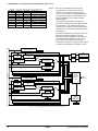
The power voltage booster generates the operating
voltage <VD2> for the LCD system voltage
regulator.
VDD
External
power
supply
VD1
VD2
CF
CG
Oscillation circuit
Internal logic
voltage regulator
Power source for
LCD system voltage regulator
VD2
VDD
VD1
OSC1, OSC2
OSC3, OSC4
Internal circuit
Power voltage
booster
VD2
VC1
VC2
VC3
VC4
VC5
CA
CB
CC
CD
CE
LCD system
voltage regulator
VC1–VC5
LCD driver
COM0–COM31
SEG0–SEG125
VSS
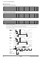
Fig. 2.2.1 Configuration of power supply circuit
S1C88650 TECHNICAL MANUAL
EPSON
7
3 CPU AND BUS CONFIGURATION
3 CPU AND BUS CONFIGURATION
In this section, we will explain the CPU, operating mode and bus configuration.
3.1 CPU
3.2.2 RAM
The S1C88650 utilize the S1C88 8-bit core CPU
whose resistor configuration, command set, etc. are
virtually identical to other units in the family of
processors incorporating the S1C88.
The internal RAM capacity is 8K bytes and is
allocated to 00D800H–00F7FFH.
Even when external memory which overlaps the
internal RAM area is expanded, the RAM area is
not released to external memory. Access to this area
is via internal RAM.
See the "S1C88 Core CPU Manual" for the S1C88.
Specifically, the S1C88650 employ the Model 3
S1C88 CPU which has a maximum address space of
1M bytes × 3.
3.2 Internal Memory
The S1C88650 is equipped with internal ROM and
RAM as shown in Figure 3.2.1. Small scale applications can be handled by one chip. It is also possible
to utilize internal memory in combination with
external memory.
Furthermore, internal ROM can be disconnected
from the bus and the resulting space released for
external applications.
0EFFFFH
Kanji font ROM
(896K bytes)
A memory mapped I/O method is employed in the
S1C88650 for interfacing with internal peripheral
circuit. Peripheral circuit control bits and data
register are arranged in data memory space.
Control and data exchange are conducted via
normal memory access. I/O memory is arranged in
page 0: 00FF00H–00FFFFH area.
See Section 5.1, "I/O Memory Map", for details of
the I/O memory.
Even when external memory which overlaps the I/
O memory area is expanded, the I/O memory area
is not released to external memory. Access to this
area is via I/O memory.
3.2.4 Display memory
010000H
00FFFFH
I/O memory
00FF00H
00FD7FH
Display memory
00F800H
00F7FFH
RAM (8K bytes)
00D800H
00D7FFH
Unused
:
area
00C000H
00BFFFH
The S1C88650 is equipped with an internal display
memory which stores a display data for LCD
driver.
Display memory is arranged in page 0: 00Fx00H–
00Fx7FH (x = 8–DH) in the data memory area. See
Section 5.11, "LCD Driver", for details of the display
memory. Like the I/O memory, display memory
cannot be released to external memory.
3.2.5 Kanji font ROM
ROM
(48K bytes)
000000H
Fig. 3.2.1 Internal memory map
3.2.1 Program ROM
The S1C88650 has a built-in 48K-byte program
ROM. The ROM is allocated to 000000H–00BFFFH.
This ROM areas shown above can be released to
external
memory depending on the setting of the
_______
MCU/MPU terminal. (See "3.5 Chip Mode".)
8
3.2.3 I/O memory
The S1C88650 has a built-in kanji font ROM that
can be used to store JIS level-1 and level-2 kanji
sets, alphanumeric characters and music shift-JIS
characters.
The kanji font ROM capacity is 896K bytes and is
allocated to 010000H–0EFFFFH.
When the kanji font is not used the remaining area
or the entire area can be used for a program and
data storage area (see the "S5U1C88xxxRx Manual"
for use of font data).
This ROM areas shown above can be released to
external
memory depending on the setting of the
_______
MCU/MPU terminal. (See "3.5 Chip Mode".)
EPSON
S1C88650 TECHNICAL MANUAL
3 CPU AND BUS CONFIGURATION
3.3 Exception Processing Vectors
000000H–00004BH in the program area of the
S1C88650 is assigned as exception processing
vectors. Furthermore, from 00004EH to 0000FFH,
software interrupt vectors are assignable to any two
bytes which begin with an even address.
Table 3.3.1 lists the vector addresses and the
exception processing factors to which they correspond.
Table 3.3.1 Exception processing vector table
Vector
address
000000H
000002H
000004H
000006H
000008H
00000AH
00000CH
00000EH
000010H
000012H
000014H
000016H
000018H
00001AH
00001CH
00001EH
000020H
000022H
000024H
000026H
000028H
00002AH
00002CH
00002EH
000030H
000032H
000034H
000036H
000038H
00003AH
00003CH
00003EH
000040H
000042H
000044H
000046H
000048H
00004AH
00004CH
00004EH
:
0000FEH
Exception processing factor
Reset
Zero division
Watchdog timer (NMI)
K07 input interrupt
K06 input interrupt
K05 input interrupt
K04 input interrupt
K03 input interrupt
K02 input interrupt
K01 input interrupt
K00 input interrupt
PTM 0 underflow interrupt
PTM 0 compare match interrupt
PTM 1 underflow interrupt
PTM 1 compare match interrupt
PTM 2 underflow interrupt
PTM 2 compare match interrupt
PTM 3 underflow interrupt
PTM 3 compare match interrupt
System reserved (cannot be used)
Serial I/F error interrupt
Serial I/F receiving complete interrupt
Serial I/F transmitting complete interrupt
System reserved (cannot be used)
System reserved (cannot be used)
System reserved (cannot be used)
Clock timer 32 Hz interrupt
Clock timer 8 Hz interrupt
Clock timer 2 Hz interrupt
Clock timer 1 Hz interrupt
PTM 4 underflow interrupt
PTM 4 compare match interrupt
PTM 5 underflow interrupt
PTM 5 compare match interrupt
PTM 6 underflow interrupt
PTM 6 compare match interrupt
PTM 7 underflow interrupt
PTM 7 compare match interrupt
System reserved (cannot be used)
Software interrupt
Priority
High
↑
When multiple exception processing factors are
generated at the same time, execution starts with
the highest priority item.
The priority sequence shown in Table 3.3.1 assumes
that the interrupt priority levels are all the same.
The interrupt priority levels can be set by software
in each system. (See Section 5.14, "Interrupt and
Standby Status".)
Note: For exception processing other than reset,
SC (system condition flag) and PC (program
counter) are evacuated to the stack and
branches to the exception processing
routines. Consequently, when returning to
the main routine from exception processing
routines, please use the RETE instruction.
See the "S1C88 Core CPU Manual" for information
on CPU operations when an exception processing
factor is generated.
3.4 CC (Customized Condition Flag)
The S1C88650 does not use the customized condition flag (CC) in the core CPU. Accordingly, it
cannot be used as a branching condition for the
conditional branching instruction (JRS, CARS).
3.5 Chip Mode
3.5.1 MCU mode and MPU mode
The chip operating mode_______
can be set to one of two
settings using the MCU/MPU terminal.
_______
■ MCU mode...Set the MCU/MPU terminal to HIGH
Switch to this setting when using internal ROM.
With respect to areas other than internal
memory, external memory can even be
expanded. See Section 3.5.2, "Bus mode", for the
memory map.
↓
Low
No
priority
rating
For each vector address and the address after it, the
start address of the exception processing routine is
written into the subordinate and super ordinate
sequence. When an exception processing factor is
generated, the exception processing routine is
executed starting from the recorded address.
S1C88650 TECHNICAL MANUAL
EPSON
In the MCU mode, during initial reset, only
systems in internal memory are activated.
Internal program ROM is normally fixed as the
top portion of the program memory from the
common area (logical space 0000H–7FFFH).
Exception processing vectors are assigned in
internal program ROM. Furthermore, the
application initialization routines that start with
reset exception processing must likewise be
written to internal program ROM. Since bus and
other settings which correlate with external
expanded memory can be executed in software,
this processing is executed in the initialization
routine written to internal program ROM. Once
these bus mode settings are made, external
memory can be accessed.
9
3 CPU AND BUS CONFIGURATION
When accessing ____
internal memory
____in this mode,
_____
the chip enable (CE) and read (RD)/write (WR)
signals are not output to external memory, and
the data bus (D0–D7) goes into high impedance
status (or pull-up status).
Consequently, in cases where addresses overlap
in external and internal memory, the areas in
external memory will be unavailable.
3.5.2 Bus mode
In order to set bus specifications to match the
configuration of external expanded memory, two
different bus modes described below are selectable
in software.
■ Single chip mode
- MCU mode -
_______
■ MPU mode...Set the MCU/MPU terminal to LOW
Internal ROM area is released to an external
device source. Internal ROM then becomes
unusable
and when this
area is accessed,
chip
____
____
_____
enable (CE) and read (RD)/write (WR) signals
are output to external memory and the data bus
(D0–D7) become active. These signals are not
output to an external source when other areas of
internal memory are accessed.
0EFFFFH
Kanji font ROM
(896K bytes)
010000H
00FFFFH
I/O memory
00FF00H
00FD7FH
Display memory
00F800H
00F7FFH
Internal RAM
00D800H
00D7FFH
:
Unused area
00C000H
00BFFFH
In the MPU mode, the system is activated by
external memory.
When employing this mode, the exception
processing vectors and initialization routine
must be assigned within the common area
(000000H–007FFFH).
Internal ROM
You can select whether
to use the built-in pull-up
_______
resistor of the MCU/MPU terminal by the mask
option.
000000H
Iput port
pull-up resistor
_______
MCU/MPU ..... ■ With resistor ■ Gate direct
Fig. 3.5.2.1 Memory map for the single chip mode
The single chip mode setting applies when the
S1C88650 is used as a single chip microcomputer without external expanded memory.
Since this mode employs internal ROM, the
system can only be operated in the MCU mode
discussed in Section 3.5.1.
In the MPU mode, the system cannot be set to
the single chip mode.
Since there is no need for an external bus line in
this mode, terminals normally set for bus use
can be used as general purpose output ports or
I/O ports.
Notes: • Setting of MCU/MPU terminal is latched at
the rising edge of a reset signal input from
the RESET terminal. Therefore, if the setting
is to be changed, the RESET terminal must
be set to LOW level once again.
• The data bus while the CPU accesses to the
internal memory can be select into highimpedance status or pulled up to high using
the pull-up control register and mask option.
See Section 5.7, "I/O Ports (P ports)", for
details.
■ Expansion mode
The expansion mode setting applies when the
S1C88650 is used with less than 1M bytes × 3 of
external expanded memory. This mode is
usable regardless of the MCU/MPU mode
setting.
Because internal ROM is being used in the MCU
mode, external memory in this model can be
assigned to the area from 100000H to 3FFFFFH.
Since the internal ROM area is released in the
MPU mode, external memory in this model can
be assigned to the area from 000000H to
2FFFFFH.
However, the area from 00C000H to 00FFFFH is
assigned to internal memory and cannot be
used to access an external device.
10
EPSON
S1C88650 TECHNICAL MANUAL
3 CPU AND BUS CONFIGURATION
- MCU mode -
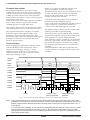
3.6 External Bus
- MPU mode -
3FFFFFH
2FFFFFH
External
memory area
:
The S1C88650 has bus terminals that can address a
maximum of 1M × 3 bytes and memory (and other)
devices can be externally expanded according to
the range of each bus mode described in the
previous section.
External
memory area
Address bus (A0–A19)
100000H
0F0000H
0EFFFFH
Data bus (D0–D7)
Unused area
S1C88650
BREQ
010000H Internal memory
00FFFFH
00D800H
00D7FFH
:
Unused area
00C000H
00BFFFH
BACK
Internal memory
External
device
External
device
External
device
RD
WR
CE0
CE1
CE2
Fig. 3.6.1 External bus lines
Below is an explanation of external bus terminals.
For information on control methods, see Section 5.2,
"System Controller and Bus Control".
External
memory area
Internal memory
3.6.1 Data bus
000000H
See Figure 3.2.1 for the internal memory
Fig. 3.5.2.2 Memory map for the expansion mode
There is an explanation on how all these settings
are actually made in "5.2 System Controller and Bus
Control" of this Manual.
3.5.3 CPU mode
The CPU allows software to select its operating
mode from two types shown below according to
the programming area size.
■ Minimum mode
The program area is configured within 64K
bytes in any one-bank. However, the bank to be
used must be specified in the CB register and
cannot be changed after an initialization. This
mode does not push the CB register contents
onto the stack when a subroutine is called. It
makes it possible to economize on stack area
usage. This mode is suitable for small- to midscale program memory and large-scale data
memory systems.
The S1C88650 possesses an 8-bit external data bus
(D0–D7). The terminals and I/O circuits of data bus
D0–D7 are shared with I/O ports P00–P07, switching between these functions being determined by
the bus mode setting.
In the single chip mode, the 8-bit terminals are all
set as I/O ports P00–P07 and in the expansion
mode, they are set as data bus (D0–D7).
When set as data bus, the data register and I/O
control register of each I/O port are detached from
the I/O circuits and usable as a general purpose
data register with read/write capabilities.
The data bus can be pulled up to high during input
mode using the built-in pull-up resistor. This pullup resistor is enabled or disabled using the pull-up
control register and mask option. See "5.7 I/O
Ports" for details.
■ Maximum mode
The program area can be configured exceeding
64K bytes. However the CB register must be
setup when the program exceeds a bank
boundary every 64K bytes. This mode pushes
the CB register contents when a subroutine is
called. This mode is suitable for large-scale
program and data memory systems.
S1C88650 TECHNICAL MANUAL
EPSON
Bus mode
Single
chip
I/O
port
Data
bus
P00
P01
P02
P03
P04
P05
P06
P07
D0
D1
D2
D3
D4
D5
D6
D7
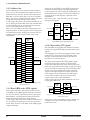
Bus mode
Expansion
Fig. 3.6.1.1 Correspondence between data bus
and I/O ports
11
3 CPU AND BUS CONFIGURATION
____
3.6.2 Address bus
The S1C88650 possesses a 20-bit external address
bus A0–A19. The terminals and output circuits of
address bus A0–A19 are shared with output ports
R00–R07 (=A0–A7), R10–R17 (=A8–A15) and R20–
R23 (=A16–A19), switching between these functions
being determined by the bus mode setting.
In the single chip mode, the 20-bit terminals are all
set as output ports R00–R07, R10–R17 and R20–R23.
In the expansion mode, all of the 20-bit terminals
are set as the address bus (A0–A19).
When set as an address bus, the data register and
high impedance control register of each output port
are detached from the output circuit and used as a
general purpose data register with read/write
capabilities.
Bus mode
Single
chip
Output
port
Address
bus
R00
R01
R02
R03
R04
A0
A1
A2
A3
A4
R05
R06
R07
R10
R11
R12
R13
R14
R15
R16
R17
R20
R21
A5
A6
A7
A8
A9
A10
A11
A12
A13
A14
A15
A16
A17
R22
R23
A18
A19
Bus mode
RD/WR
signal
R24
RD
Bus mode
Expansion
R25
WR
____
Fig. 3.6.3.1 Correspondence
between read (RD)/
_____
write (WR) signal and output ports
_____
3.6.4 Chip enable (CE) signal
The S1C88650 is equipped with address decoders
____
which can output three different chip enable (CE)
signals.
Consequently,
three devices
_____
_____equipped with a chip
enable (CE) or chip select (CS) terminal can be
directly connected without setting the address
decoder to an external device.
Bus mode
_____ _____
The three chip enable (CE0–CE2) signal output
terminals and output circuits are shared with
output ports R30–R32 and
____ in the expansion mode,
either the chip enable (CE) output or general output
can be selected in software____
for each of the three bits.
When set for chip enable (CE) output, the data
register and high impedance control register for
each output port are detached from the output
circuit and is usable as general purpose data
register with read/write capabilities.
In the single chip mode, these terminals are set as
output ports R30–R32.
Expansion
Bus mode
______
3.6.3 Read (RD)/write (WR) signals
The output
terminals
____
_____ and output circuits for the
read (RD)/write (WR) signals directed to external
devices are shared respectively with output ports
R24 and R25, switching between these functions
being determined by the bus mode setting.
In the single chip mode, both of these terminals are
set as output port terminals____
and in the expansion
_____
mode, they are set as read (RD)/write (WR) signal
output terminals.
12
Output
port
Single
chip
Fig. 3.6.2.1 Correspondence between address bus
and output ports
_____
_____
When set as read (RD)/write (WR) signal output
terminal, the data register and high impedance
control register for each output port (R24, R25) are
detached from the output circuit and is usable as a
general purpose data register with read/write
capabilities.
See Section 3.6.5, "WAIT control", for the output
timing of the signal.
Single
chip
Output
port
CE
signal
R30
CE0
R31
R32
CE1
CE2
Bus mode
Expansion
____
Fig. 3.6.4.1 Correspondence between CE signals
and output ports
Table 3.6.4.1 shows the address
____ ranges which are
assigned to the chip enable (CE) signal in the
expansion mode.
EPSON
S1C88650 TECHNICAL MANUAL
3 CPU AND BUS CONFIGURATION
_____ _____
Table 3.6.4.1 CE0–CE2 address settings
Address range (expansion mode)
MCU mode
MPU mode
300000H–3FFFFFH
000000H–00D7FFH, 010000H–0FFFFFH
100000H–1FFFFFH
100000H–1FFFFFH
200000H–2FFFFFH
200000H–2FFFFFH
CE signal
CE0
CE1
CE2
_____
When accessing the internal memory area, the CE
signal is not output. Care should be taken here
because the address range for these portions of
memory involves irregular settings.
The arrangement of memory space for external
devices does not necessarily have to be continuous
from a subordinate address and any of the chip
enable signals can be used to assign areas in
memory.
Table 3.6.5.1 Selectable WAIT state numbers
Selection No.
Insert states
1
0
2
2
3
4
4
6
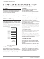
5
8
6
10
7
12
8
14
* One state is a 1/2 cycle of the clock in length.
Note: The CE signals will be inactive status when
the chip enters the standby mode (HALT
mode or SLEEP mode).
The WAIT states set in software are inserted
between bus cycle states T3–T4.
Note, however, that WAIT states cannot be inserted
when an internal register and internal memory are
being accessed and when operating with the OSC1
oscillation circuit (see "5.4 Oscillation Circuits").
Consequently, WAIT state settings are meaningless
in the single chip mode.
See Section 3.6.5, "WAIT control", for the output
timing of signal.
Figure 3.6.5.1 shows the memory read/write
timing charts.
____
T1
3.6.5 WAIT control
T2
T3
T4
T1
T2
T3
T4
CLK
In order to insure accessing of external low speed
devices during high speed operations, the S1C88650
is equipped with a WAIT function which prolongs
access time. (See the "S1C88 Core CPU Manual" for
details of the WAIT function.)
A0–A19
Address
Address
CE0
CE1
The WAIT state numbers to be inserted can be
selected in software from a series of 8 as shown in
Table 3.6.5.1.
WR
RD
D0–D7
Read data
Read cycle
Write data
Write cycle
(1) No WAIT
WAIT (4 states inserted)
T1
T2
T3 Tw1 Tw2 Tw1 Tw2
WAIT (4 states inserted)
T4
T1
T2
T3 Tw1 Tw2 Tw1 Tw2 T4
CLK
A0–A19
Address
Address
CE0
CE1
WR
RD
D0–D7
Read data
Write data
Read cycle
Write cycle
(2) WAIT state insertion
Fig. 3.6.5.1 Memory read/write cycle
S1C88650 TECHNICAL MANUAL
EPSON
13
3 CPU AND BUS CONFIGURATION
________
When the bus authority release request (BREQ =
LOW) is received from an external device, the____
S1C88650 switches
_____
____ the address bus, data bus, RD/
WR signal, and CE signal lines to a high
impedance
________
state, outputs a LOW level from the BACK terminal
and releases bus authority.
________
As soon as a LOW level is output from the BACK
terminal, the external device can use the external
bus. When DMA
________is completed, the external device
returns the BREQ terminal to HIGH and releases
bus authority.
Figure 3.6.6.2 shows the bus authority release
sequence.
3.6.6 Bus authority release state
The S1C88650 is equipped with a bus authority
release function on request from an external device
so that DMA (Direct Memory Access) transfer can
be conducted between external devices. The
internal memory cannot be accessed by this
function.
There are two terminals used for this________
function: the
bus authority release request signal (BREQ) input
terminal________
and the bus authority release acknowledge
signal
(BACK)
output terminal.
________
The BREQ input terminal
is shared with input port
________
terminal K03 and the BACK output terminal with
output
terminal R33, use with setting to
________ port
________
BREQ/BACK terminals done in software. In the
single chip mode, or when using a system which
does not require bus authority release, set respective terminals as input and output ports.
Input
port
K03
Output
port
R33
During bus authority release state, internal memory
cannot be accessed from the external device. In
cases where external memory has areas which
overlap areas in internal memory, the external
memory
areas can be accessed accordance with the
____
CE signal output by the external device.
Note: Be careful with the system, such that an
external device does not become the bus
master, other than during the bus release
status.
_______
After setting the_______
BREQ terminal to LOW
level, hold
the BREQ terminal at LOW level
_______
until the
BACK
terminal becomes LOW level.
_______
If the BREQ terminal
is returned to HIGH
_______
level, before the BACK terminal becomes
LOW level, the shift to the bus authorization
release status will become indefinite.
BREQ
input
BACK
output
_______ _______
Fig. 3.6.6.1 BREQ/BACK terminals
Tw2
T4
T1
T2
T3
Tw1
Tw2
T4
Tz1
Tz2
Tz1
Tz2
Tz1
Tz2
Tz1
Tz2
T1
T2
T3
CLK
A0–A19
IX
D0–D7
(IX)
HL
PC
(IX)
ANY
WR
RD
BREQ
L
L
L
L
H
BACK
Program exection status
Bus authority release status
Program
exection
status
LD [HL],[IX]
Fig. 3.6.6.2 Bus authority release sequence
14
EPSON
S1C88650 TECHNICAL MANUAL
4 INITIAL RESET
4 INITIAL RESET
Initial reset in the S1C88650 is required in order to initialize circuits. This section of the Manual
contains a description of initial reset factors and the initial settings for internal registers, etc.
____________
4.1 Initial Reset Factors
4.1.1 RESET terminal
There are two initial reset factors for the S1C88650
as shown below.
Initial reset can be_________
done by externally inputting a
LOW level to the RESET_________
terminal.
Be sure to maintain the RESET terminal at LOW
level for the regulation time after the power on to
assure the initial reset. (See Section 8.6, "AC
Characteristics".)
_________
In addition, be sure to use the RESET terminal for
the first
initial reset after the power is turned on.
_________
The RESET terminal is equipped with a pull-up
resistor. You can select whether or not to use by
mask option.
_________
(1) External initial reset by the RESET terminal
(2) External initial reset by the simultaneous LOW
level input at input port terminals K00–K03
(mask option)
Figure 4.1.1 shows the configuration of the initial
reset circuit.
The CPU and peripheral circuits are initialized by
means of initial reset factors. When the factor is
canceled, the CPU commences reset exception
processing. (See the "S1C88 Core CPU Manual".)
When this occurs, the reset exception processing
vector, Bank 0, 000000H–000001H from program
memory is read out and the program (initialization
routine) which begins at the readout address is
executed.
Input
port pull-up resistor
_________
RESET ............ ■ With resistor
■ Gate direct
Operating clock status
OSC3
OSC4
OSC3
oscillation
circuit
Divider
fOSC3/1,024 Hz
Selector
OSC1
OSC2
fOSC1/256 Hz
OSC1
oscillation
circuit
Divider
Reset release
clock
K00
Input port K00
K01
Input port K01
K02
Input port K01
K03
Input port K03
Time
authorize
circuit
Internal initial
reset
R
Reset signal
Q
S
SLEEP status
Oscillation stability
waiting signal
VDD
Mask
option
RESET
Fig. 4.1.1 Configuration of initial reset circuit
S1C88650 TECHNICAL MANUAL
EPSON
15
4 INITIAL RESET
4.1.2 Simultaneous LOW level input at
input port terminals K00–K03
4.1.3 Initial reset sequence
Another way of executing initial reset externally is
to input a LOW level simultaneously to the input
ports (K00–K03) selected by mask option.
Since there is a built-in time authorize circuit, be
sure to maintain the designated input port terminal
at LOW level for 65536/fOSC1 seconds (two seconds
when the oscillation frequency is fOSC1 = 32.768
kHz) or more to perform the initial reset by means
of this function.
However, the time authorize circuit is bypassed
during the SLEEP (standby) status and oscillation
stabilization waiting period, and initial reset is
executed immediately after the simultaneous LOW
level input to the designated input ports.
The combination of input ports (K00–K03) that can
be selected by mask option are as follows:
Multiple key entry reset
■ Not use
■ K00 & K01
■ K00 & K01 & K02
■ K00 & K01 & K02 & K03
For instance, let's say that mask option "K00 & K01
& K02 & K03" is selected, when the input level at
input ports K00–K03 is simultaneously LOW, initial
reset will take place.
When using this function, make sure that the
designated input ports do not simultaneously
switch to LOW level while the system is in normal
operation.
After
cancellation of the LOW level input to the
_________
RESET terminal, when the power is turned on, the
start-up of the CPU is held back until the oscillation
stabilization waiting time (512/fOSC3 sec.) have
elapsed.
Figure 4.1.3.1 shows the operating sequence
following initial reset release.
The CPU starts operating in synchronization with
the OSC3 clock after reset status is released.
Also, when using the initial reset by simultaneous
LOW level input into the input port, you should be
careful of the following points.
(1) During SLEEP status, since the time authorization circuit is bypassed, an initial reset is
triggered immediately after a LOW level
simultaneous input value. In this case, the CPU
starts after waiting the oscillation stabilization
time, following cancellation of the LOW level
simultaneous input.
(2) Other than during SLEEP status, an initial reset
will be triggered 65536/fOSC3 seconds after a
LOW level simultaneous input. In this case,
since a reset differential pulse (64/fOSC1
seconds) is generated within the S1C88650, the
CPU will start even if the LOW level
simultaneous input status is not canceled.
Note: The oscillation stabilization time described in
this section does not include oscillation start
time. Therefore the time interval until the
CPU starts executing instructions after
power is turned on or SLEEP status is
cancelled may be longer than that indicated
in the figure below.
fOSC3
Reset signal
Reset release
Reset release clock
Internal initial reset release
Internal initial reset
Internal address bus
PC
Internal data bus
PC
PC
Dummy
Dummy
00-0000
VECL
Internal read signal
512/fOSC3 [sec]
Oscillation stable waiting time
Dummy cycle
Reset exception processing
∗ Reset status is maintained
during this period.
Fig. 4.1.3.1 Initial reset sequence
16
EPSON
S1C88650 TECHNICAL MANUAL
4 INITIAL RESET
4.2 Initial Settings After Initial Reset
The CPU internal registers are initialized as follows
during initial reset.
Table 4.2.1 Initial settings
Register name
Code Bit length Setting value
Data register A
A
8
Undefined
Data register B
B
8
Undefined
Index (data) register L
L
8
Undefined
Index (data) register H
H
8
Undefined
Index register IX
IX
16
Undefined
Index register IY
IY
16
Undefined
Program counter
PC
16
Undefined *
Stack pointer
SP
16
Undefined
Base register
BR
8
Undefined
Zero flag
Z
1
0
Carry flag
C
1
0
Overflow flag
V
1
0
Negative flag
N
1
0
Decimal flag
D
1
0
Unpack flag
U
1
0
Interrupt flag 0
I0
1
1
Interrupt flag 1
I1
1
1
New code bank register
NB
8
01H
Code bank register
CB
8
Undefined *
Expand page register
EP
8
00H
Expand page register for IX XP
8
00H
Expand page register for IY YP
8
00H
* Reset exception processing loads the preset
values stored in 0 bank, 0000H–0001H into the
PC. At the same time, 01H of the NB initial
value is loaded into CB.
Initialize the registers which are not initialized at
initial reset using software.
Since the internal RAM and display memory are
not initialized at initial reset, be sure to initialize
using software.
The respectively stipulated initializations are done
for internal peripheral circuits. If necessary, the
initialization should be done using software.
For initial value at initial reset, see the sections on
the I/O memory map and peripheral circuit
descriptions in the following chapter of this
manual.
S1C88650 TECHNICAL MANUAL
EPSON
17
5 PERIPHERAL CIRCUITS AND THEIR OPERATION (I/O Memory Map)
5 PERIPHERAL CIRCUITS AND
THEIR OPERATION
The peripheral circuits of the S1C88650 is interfaced with the CPU by means of the memory mapped
I/O method. For this reason, just as with other memory access operations, peripheral circuits can be
controlled by manipulating I/O memory. Below is a description of the operation and control method for
each individual peripheral circuit.
5.1 I/O Memory Map
Table 5.1.1(a) I/O Memory map (00FF00H–00FF03H)
Address Bit Name
Function
00FF00 D7 BUSMOD Bus mode
(MCU) D6 CPUMOD CPU mode
D5 –
R/W register
D4 –
R/W register
D3 –
R/W register
D2 CE2
CE2 (R32) CE signal output Enable/Disable
D1 CE1
CE1 (R31) Enable: CE signal output
D0 CE0
CE0 (R30) Disable: DC (R3x) output
00FF00 D7 BUSMOD Bus mode
(MPU) D6 CPUMOD CPU mode
D5 –
R/W register
D4 –
R/W register
D3 –
R/W register
D2 CE2
CE2 (R32) CE signal output Enable/Disable
D1 CE1
CE1 (R31) Enable: CE signal output
D0 CE0
CE0 (R30) Disable: DC (R3x) output
00FF01 D7 SPP7
Stack pointer page address
(MSB)
D6 SPP6
D5 SPP5
< SP page allocatable address >
D4 SPP4
• Single chip mode: only 0 page
D3 SPP3
• Expansion mode: 0–27H page
D2 SPP2
D1 SPP1
D0 SPP0
(LSB)
00FF02 D7 EBR
Bus release enable register
K03
(K03 and R33 terminal specification)
R33
D6 WT2
Wait control register
Number
WT2
WT1
WT0
of state
1
1
1
14
1
1
0
12
D5 WT1
1
0
1
10
1
0
0
8
0
1
1
6
0
1
0
D4 WT0
4
0
0
1
2
0
0
0
No wait
D3
D2
D1
D0
00FF03 D7
D6
D5
D4
D3
D2
D1
D0
Note:
18
CLKCHG
SOSC3
–
–
–
–
–
–
–
–
VDSEL
DBON
CPU operating clock switch
OSC3 oscillation On/Off control
R/W register
R/W register
–
–
–
–
–
–
Power source select for LCD voltage regulator
Power voltage booster On/Off control
____
1
0
Expansion
Single chip
Maximum
Minimum
1
0
1
0
1
0
CE2 enable
CE2 disable
CE1 enable
CE1 disable
CE0 enable
CE0 disable
Expansion
–
Maximum
Minimum
1
0
1
0
1
0
CE2 enable
CE2 disable
CE1 enable
CE1 disable
CE0 enable
CE0 disable
1
0
1
0
1
0
1
0
1
0
1
0
1
0
1
0
BREQ
Input port
BACK
Output port
OSC3
OSC1
On
Off
1
0
1
0
–
–
–
–
–
–
–
–
–
–
–
–
VD2
VDD
On
Off
SR
0
0
0
0
0
0
0
0
1
0
0
0
0
0
0
1
0
0
0
0
0
0
0
0
0
R/W
R/W
R/W
R/W
R/W
R/W
R/W
R/W
R/W
R
R/W
R/W
R/W
R/W
R/W
R/W
R/W
R/W
R/W
R/W
R/W
R/W
R/W
R/W
R/W
R/W
Comment
0
R/W
0
R/W
0
R/W
1
1
0
0
–
–
–
–
–
–
0
0
R/W
R/W
R/W Reserved register
R/W
Reserved register
In Single chip mode,
these setting are fixed
at DC output.
Expansion mode only
Reserved register
Constantly "0" when
being read
R/W
R/W
All the interrupts including NMI are disabled, until you write the optional value into both the "00FF00H" and
"00FF01H" addresses.
EPSON
S1C88650 TECHNICAL MANUAL
5 PERIPHERAL CIRCUITS AND THEIR OPERATION (I/O Memory Map)
Table 5.1.1(b) I/O Memory map (00FF10H–00FF14H)
Address Bit Name
Function
00FF10 D7 HLMOD Heavy load protection mode
D6 SEGREV Reverse SEG assignment
D5 –
R/W register
D4 –
D3 –
D2 DTFNT
R/W register
R/W register
LCD dot font selection
D1 LDUTY1 LCD drive duty selection
Duty
LDUTY1 LDUTY0
Not allowed
1
1
D0 LDUTY0
1/16
0
1
1/32
1
0
1/8
0
0
00FF11 D7 FRMCS LCD frame signal source clock selection
D6 DSPAR LCD display memory area selection
D5 LCDC1
D4 LCDC0
D3 LC3
LC3 LC2 LC1 LC0
1
1
1
1
1
1
1
0
:
:
:
:
0
0
0
0
D1 LC1
D0 LC0
D2 SVDS2
D1 SVDS1
D0 SVDS0
D4 PST10
D0 PST00
0
0
0
1
0
0
R/W
R/W Reserved register
R/W
1
0
12×12
16×16/5×8
0
0
R/W
R/W
1
R/W
0
R/W
0
0
R/W
R/W
0
R/W These bits are reset
0
to (0, 0) when
SLP instruction
R/W is executed.
PTM
fOSC1
R/W
0
R/W
:
:
0
R/W
0
R/W
Light
–
–
–
–
–
–
Low
Normal
On
Off
SVD criteria voltage setting
SVDS3 SVDS2 SVDS1 SVDS0 Voltage (V)
2.7
1
1
1
1
2.6
1
1
1
0
2.5
1
1
0
1
:
:
:
:
:
1.8
0
0
1
1
PST12 PST11 PST10 (OSC3)
1
1
1
fOSC3 / 4096
fOSC3 / 1024
1
1
0
fOSC3 / 256
1
0
1
fOSC3 / 64
1
0
0
fOSC3 / 32
0
1
1
fOSC3 / 8
0
1
0
fOSC3 / 2
0
0
1
fOSC3 / 1
0
0
0
PST02 PST01 PST00 (OSC3)
1
1
1
fOSC3 / 4096
fOSC3 / 1024
1
1
0
fOSC3 / 256
1
0
1
fOSC3 / 64
1
0
0
fOSC3 / 32
0
1
1
fOSC3 / 8
0
1
0
fOSC3 / 2
0
0
1
fOSC3 / 1
0
0
0
S1C88650 TECHNICAL MANUAL
On
Off
(OSC1)
fOSC1 / 128
fOSC1 / 64
fOSC1 / 32
fOSC1 / 16
fOSC1 / 8
fOSC1 / 4
fOSC1 / 2
fOSC1 / 1
D3 PRPRT0 Programmable timer 0 clock control
D2 PST02 Programmable timer 0 division ratio
D1 PST01
Normal
1
0
00FF14 D7 PRPRT1 Programmable timer 1 clock control
D6 PST12 Programmable timer 1 division ratio
D5 PST11
Reverse
Display area 1 Display area 0
SR R/W
0 R/W
Contrast
Dark
D5 SVDDT SVD detection data
D4 SVDON SVD circuit On/Off
D3 SVDS3
0
Off
LCD display control
LCD display
LCDC1 LCDC0
1
1
All LCDs lit
1
0
All LCDs out
0
1
Normal display
0
0
Drive off
LCD contrast adjustment
D2 LC2
00FF12 D7 –
D6 –
1
On
(OSC1)
fOSC1 / 128
fOSC1 / 64
fOSC1 / 32
fOSC1 / 16
fOSC1 / 8
fOSC1 / 4
fOSC1 / 2
fOSC1 / 1
EPSON
On
Off
–
–
Comment
Constantly "0" when
being read
0
0
R
R/W
0
R/W
0
R/W
0
R/W
0
R/W
0
0
R/W
R/W
0
R/W
0
R/W
0
0
R/W
R/W
0
R/W
0
R/W
19
5 PERIPHERAL CIRCUITS AND THEIR OPERATION (I/O Memory Map)
Table 5.1.1(c) I/O Memory map (00FF15H–00FF18H)
Address Bit Name
Function
00FF15 D7 PRPRT3 Programmable timer 3 clock control
D6 PST32 Programmable timer 3 division ratio
D5 PST31
D4 PST30
PST32 PST31 PST30 (OSC3)
1
1
1
fOSC3 / 4096
fOSC3 / 1024
1
1
0
fOSC3 / 256
1
0
1
fOSC3 / 64
1
0
0
fOSC3 / 32
0
1
1
fOSC3 / 8
0
1
0
fOSC3 / 2
0
0
1
fOSC3 / 1
0
0
0
D1 PST21
D0 PST20
00FF17 D7
D6
D5
D4
D3
D2
D1
D0
00FF18 D7
D6
–
–
–
–
PRTF3
PRTF2
PRTF1
PRTF0
PRPRT5
PST52
D5 PST51
D4 PST50
D1 PST41
D0 PST40
20
Off
–
–
–
–
–
–
1
0
fOSC1
fOSC3
fOSC1
fOSC3
fOSC1
fOSC3
fOSC1
fOSC3
On
Off
(OSC1)
fOSC1 / 128
fOSC1 / 64
fOSC1 / 32
fOSC1 / 16
fOSC1 / 8
fOSC1 / 4
fOSC1 / 2
fOSC1 / 1
D3 PRPRT4 Programmable timer 4 clock control
D2 PST42 Programmable timer 4 division ratio
PST42 PST41 PST40 (OSC3)
1
1
1
fOSC3 / 4096
fOSC3 / 1024
1
1
0
fOSC3 / 256
1
0
1
fOSC3 / 64
1
0
0
fOSC3 / 32
0
1
1
fOSC3 / 8
0
1
0
fOSC3 / 2
0
0
1
fOSC3 / 1
0
0
0
On
(OSC1)
fOSC1 / 128
fOSC1 / 64
fOSC1 / 32
fOSC1 / 16
fOSC1 / 8
fOSC1 / 4
fOSC1 / 2
fOSC1 / 1
–
–
–
R/W register
Programmable timer 3 source clock selection
Programmable timer 2 source clock selection
Programmable timer 1 source clock selection
Programmable timer 0 source clock selection
Programmable timer 5 clock control
Programmable timer 5 division ratio
PST52 PST51 PST50 (OSC3)
1
1
1
fOSC3 / 4096
fOSC3 / 1024
1
1
0
fOSC3 / 256
1
0
1
fOSC3 / 64
1
0
0
fOSC3 / 32
0
1
1
fOSC3 / 8
0
1
0
fOSC3 / 2
0
0
1
fOSC3 / 1
0
0
0
0
Off
(OSC1)
fOSC1 / 128
fOSC1 / 64
fOSC1 / 32
fOSC1 / 16
fOSC1 / 8
fOSC1 / 4
fOSC1 / 2
fOSC1 / 1
D3 PRPRT2 Programmable timer 2 clock control
D2 PST22 Programmable timer 2 division ratio
PST22 PST21 PST20 (OSC3)
1
1
1
fOSC3 / 4096
fOSC3 / 1024
1
1
0
fOSC3 / 256
1
0
1
fOSC3 / 64
1
0
0
fOSC3 / 32
0
1
1
fOSC3 / 8
0
1
0
fOSC3 / 2
0
0
1
fOSC3 / 1
0
0
0
1
On
(OSC1)
fOSC1 / 128
fOSC1 / 64
fOSC1 / 32
fOSC1 / 16
fOSC1 / 8
fOSC1 / 4
fOSC1 / 2
fOSC1 / 1
EPSON
On
Off
SR R/W
0 R/W
0 R/W
0
R/W
0
R/W
0
0
R/W
R/W
0
R/W
0
R/W
Comment
–
–
–
0
0
0
0
0
0
0
R/W Reserved register
R/W
R/W
R/W
R/W
R/W
R/W
0
R/W
0
R/W
0
0
R/W
R/W
0
R/W
0
R/W
Constantly "0" when
being read
S1C88650 TECHNICAL MANUAL
5 PERIPHERAL CIRCUITS AND THEIR OPERATION (I/O Memory Map)
Table 5.1.1(d) I/O Memory map (00FF19H–00FF22H)
Address Bit Name
Function
00FF19 D7 PRPRT7 Programmable timer 7 clock control
D6 PST72 Programmable timer 7 division ratio
D5 PST71
D4 PST70
PST72 PST71 PST70 (OSC3)
1
1
1
fOSC3 / 4096
fOSC3 / 1024
1
1
0
fOSC3 / 256
1
0
1
fOSC3 / 64
1
0
0
fOSC3 / 32
0
1
1
fOSC3 / 8
0
1
0
fOSC3 / 2
0
0
1
fOSC3 / 1
0
0
0
D1 PST61
D0 PST60
00FF1B D7
D6
D5
D4
D3
D2
D1
D0
00FF20 D7
D6
D5
D4
D3
D2
D1
–
–
–
–
PRTF7
PRTF6
PRTF5
PRTF4
PK01
PK00
PSIF1
PSIF0
–
–
PTM1
On
Off
(OSC1)
fOSC1 / 128
fOSC1 / 64
fOSC1 / 32
fOSC1 / 16
fOSC1 / 8
fOSC1 / 4
fOSC1 / 2
fOSC1 / 1
–
–
–
–
Programmable timer 7 source clock selection
Programmable timer 6 source clock selection
Programmable timer 5 source clock selection
Programmable timer 4 source clock selection
K00–K07 interrupt priority register
Serial interface interrupt priority register
–
–
Clock timer interrupt priority register
D0 PTM0
00FF21 D7
D6
D5
D4
0
Off
(OSC1)
fOSC1 / 128
fOSC1 / 64
fOSC1 / 32
fOSC1 / 16
fOSC1 / 8
fOSC1 / 4
fOSC1 / 2
fOSC1 / 1
D3 PRPRT6 Programmable timer 6 clock control
D2 PST62 Programmable timer 6 division ratio
PST62 PST61 PST60 (OSC3)
1
1
1
fOSC3 / 4096
fOSC3 / 1024
1
1
0
fOSC3 / 256
1
0
1
fOSC3 / 64
1
0
0
fOSC3 / 32
0
1
1
fOSC3 / 8
0
1
0
fOSC3 / 2
0
0
1
fOSC3 / 1
0
0
0
1
On
–
–
–
–
–
–
–
–
fOSC1
fOSC3
fOSC1
fOSC3
fOSC1
fOSC3
fOSC1
PK01 PK00
PSIF1 PSIF0
1
1
0
1
1
0
0
0
–
fOSC3
Priority
level
Level 3
Level 2
Level 1
Level 0
–
–
–
PTM1 PTM0 Priority level
Level 3
1
1
Level 2
1
0
Level 1
0
1
Level 0
0
0
SR R/W
0 R/W
0 R/W
0
R/W
0
R/W
0
0
R/W
R/W
0
R/W
0
R/W
–
–
–
–
0
0
0
0
0
R/W
R/W
R/W
R/W
R/W
0
R/W
–
–
0
Comment
Constantly "0" when
being read
Constantly "0" when
being read
R/W
–
–
PPT3
PPT2
–
–
Programmable timer 3–2 interrupt
priority register
D3 PPT1
D2 PPT0
D1 –
Programmable timer 1–0 interrupt
priority register
–
–
–
–
Constantly "0" when
D0 –
–
–
–
–
being read
00FF22 D7 –
D6 –
D5 –
–
–
–
–
–
Constantly "0" when
–
–
–
–
–
–
–
–
–
–
–
Interrupt
Interrupt
enable
disable
D4
D3
D2
D1
–
ETM32
ETM8
ETM2
D0 ETM1
–
–
PPT3 PPT2
PPT1 PPT0
1
1
1
0
0
1
0
0
–
–
Priority
level
Level 3
Level 2
Level 1
– 0
Level
–
–
Constantly "0" when
being read
0
R/W
0
R/W
being read
Clock timer 32 Hz interrupt enable register
Clock timer 8 Hz interrupt enable register
Clock timer 2 Hz interrupt enable register
Clock timer 1 Hz interrupt enable register
S1C88650 TECHNICAL MANUAL
EPSON
0
R/W
21
5 PERIPHERAL CIRCUITS AND THEIR OPERATION (I/O Memory Map)
Table 5.1.1(e) I/O Memory map (00FF23H–00FF28H)
Address Bit
Name
00FF23 D7
D6
D5
D4
D3
D2
D1
D0
00FF24 D7
D6
D5
D4
D3
D2
D1
D0
00FF25 D7
D6
D5
D4
D3
D2
D1
D0
00FF26 D7
D6
D5
D4
D3
D2
D1
D0
00FF27 D7
D6
D5
D4
D3
D2
D1
D0
00FF28 D7
D6
D5
D4
D3
D2
D1
D0
–
–
–
–
–
ESERR
ESREC
ESTRA
EK07
EK06
EK05
EK04
EK03
EK02
EK01
EK00
ETC3
ETU3
ETC2
ETU2
ETC1
ETU1
ETC0
ETU0
–
–
–
–
FTM32
FTM8
FTM2
FTM1
–
–
–
–
–
FSERR
FSREC
FSTRA
FK07
FK06
FK05
FK04
FK03
FK02
FK01
FK00
22
Function
1
0
–
–
–
–
–
–
–
–
–
–
–
–
–
–
–
Serial I/F (error) interrupt enable register
Interrupt
Interrupt
Serial I/F (receiving) interrupt enable register
enable
disable
Serial I/F (transmitting) interrupt enable register
K07 interrupt enable
K06 interrupt enable
K05 interrupt enable
K04 interrupt enable
Interrupt
Interrupt
K03 interrupt enable
enable
disable
K02 interrupt enable
K01 interrupt enable
K00 interrupt enable
PTM3 compare match interrupt enable
PTM3 underflow interrupt enable
PTM2 compare match interrupt enable
Interrupt
Interrupt
PTM2 underflow interrupt enable
enable
disable
PTM1 compare match interrupt enable
PTM1 underflow interrupt enable
PTM0 compare match interrupt enable
PTM0 underflow interrupt enable
–
–
–
–
–
–
–
–
–
–
–
–
Clock timer 32 Hz interrupt factor flag
(R)
(R)
Clock timer 8 Hz interrupt factor flag
Generated Not generated
Clock timer 2 Hz interrupt factor flag
(W)
(W)
Clock timer 1 Hz interrupt factor flag
No operation
Reset
–
–
–
–
–
–
–
–
–
–
–
–
–
–
–
Serial I/F (error) interrupt factor flag
Serial I/F (receiving) interrupt factor flag
Serial I/F (transmitting) interrupt factor flag
K07 interrupt factor flag
K06 interrupt factor flag
K05 interrupt factor flag
K04 interrupt factor flag
K03 interrupt factor flag
K02 interrupt factor flag
K01 interrupt factor flag
K00 interrupt factor flag
EPSON
(R)
(R)
Generated Not generated
(W)
(W)
Reset
No operation
(R)
(R)
Interrupt
No interrupt
factor is
factor is
generated
generated
(W)
(W)
Reset
No operation
SR R/W
–
–
–
–
–
being read
0
R/W
0
R/W
0
R/W
–
–
–
–
0
Comment
Constantly "0" when
Constantly "0" when
being read
R/W
–
–
–
–
–
Constantly "0" when
being read
0
R/W
0
R/W
S1C88650 TECHNICAL MANUAL
5 PERIPHERAL CIRCUITS AND THEIR OPERATION (I/O Memory Map)
Table 5.1.1(f) I/O Memory map (00FF29H–00FF31H)
Address Bit Name
00FF29 D7 FTC3
D6 FTU3
D5 FTC2
D4 FTU2
D3 FTC1
D2 FTU1
D1 FTC0
D0 FTU0
00FF2A D7 –
D6 –
D5 –
D4 –
D3 PPT7
D2 PPT6
D1 PPT5
D0 PPT4
00FF2C D7 ETC7
D6 ETU7
D5 ETC6
D4 ETU6
D3 ETC5
D2 ETU5
D1 ETC4
D0 ETU4
00FF2E D7 FTC7
D6 FTU7
D5 FTC6
D4 FTU6
D3 FTC5
D2 FTU5
D1 FTC4
D0 FTU4
00FF30 D7 MODE16_A
D6 PTNREN_A
D5 –
D4 –
D3 PTOUT0
D2 PTRUN0
D1 PSET0
D0 CKSEL0
00FF31 D7 –
D6 –
D5 –
D4 –
D3 PTOUT1
D2 PTRUN1
D1 PSET1
D0 CKSEL1
Function
PTM3 compare match interrupt factor flag
PTM3 underflow interrupt factor flag
PTM2 compare match interrupt factor flag
PTM2 underflow interrupt factor flag
PTM1 compare match interrupt factor flag
PTM1 underflow interrupt factor flag
PTM0 compare match interrupt factor flag
PTM0 underflow interrupt factor flag
–
–
–
–
Programmable timer 7–6 interrupt
priority register
Programmable timer 5–4 interrupt
priority register
PTM7 compare match interrupt enable
PTM7 underflow interrupt enable
PTM6 compare match interrupt enable
PTM6 underflow interrupt enable
PTM5 compare match interrupt enable
PTM5 underflow interrupt enable
PTM4 compare match interrupt enable
PTM4 underflow interrupt enable
PTM7 compare match interrupt factor flag
PTM7 underflow interrupt factor flag
PTM6 compare match interrupt factor flag
PTM6 underflow interrupt factor flag
PTM5 compare match interrupt factor flag
PTM5 underflow interrupt factor flag
PTM4 compare match interrupt factor flag
PTM4 underflow interrupt factor flag
PTM0–1 8/16-bit mode selection
External clock 0 noise rejecter selection
–
R/W register
PTM0 clock output control
PTM0 Run/Stop control
PTM0 preset
PTM0 input clock selection
–
–
–
R/W register
PTM1 clock output control
PTM1 Run/Stop control
PTM1 preset
PTM1 input clock selection
S1C88650 TECHNICAL MANUAL
EPSON
1
0
(R)
(R)
Interrupt
No interrupt
factor is
factor is
generated
generated
(W)
(W)
Reset
No operation
–
–
–
–
–
–
–
PPT7 PPT6
PPT5 PPT4
1
1
1
0
0
1
0
0
–
Priority
level
Level 3
Level 2
Level 1
Level 0
Interrupt
Interrupt
enable
disable
(R)
(R)
Interrupt
No interrupt
factor is
factor is
generated
generated
(W)
(W)
Reset
No operation
16-bit x 1
8-bit x 2
Enable
Disable
–
–
1
0
On
Off
Run
Stop
Preset
No operation
External clock Internal clock
–
–
–
–
–
–
1
0
On
Off
Run
Stop
Preset
No operation
External clock Internal clock
SR R/W
0
Comment
R/W
–
–
–
–
0
R/W
0
R/W
0
R/W
0
R/W
0
0
–
0
0
0
0
0
–
–
–
0
0
0
0
0
R/W
R/W
Constantly "0" when
being read
"0" when being read
R/W Reserved register
R/W
R/W
W "0" when being read
R/W
Constantly "0" when
being read
R/W Reserved register
R/W
R/W
W "0" when being read
R/W
23
5 PERIPHERAL CIRCUITS AND THEIR OPERATION (I/O Memory Map)
Table 5.1.1(g) I/O Memory map (00FF32H–00FF37H)
Address Bit Name
00FF32 D7 RDR07
D6 RDR06
D5 RDR05
PTM0 reload data D6
PTM0 reload data D5
D4 RDR04
PTM0 reload data D4
D3 RDR03
D2 RDR02
PTM0 reload data D3
PTM0 reload data D2
D1 RDR01
PTM0 reload data D1
D0 RDR00
PTM0 reload data D0 (LSB)
00FF33 D7 RDR17
PTM1 reload data D7 (MSB)
D6 RDR16
D5 RDR15
PTM1 reload data D6
PTM1 reload data D5
D4 RDR14
D3 RDR13
PTM1 reload data D4
PTM1 reload data D3
D2 RDR12
D1 RDR11
D0 RDR10
PTM1 reload data D2
PTM1 reload data D1
PTM1 reload data D0 (LSB)
00FF34 D7 CDR07
D6 CDR06
D5 CDR05
D4 CDR04
D3 CDR03
D2
D1
D0
00FF35 D7
D6
24
Function
PTM0 reload data D7 (MSB)
CDR02
CDR01
CDR00
CDR17
CDR16
1
0
SR R/W
High
Low
1
R/W
High
Low
1
R/W
High
Low
0
R/W
High
Low
0
R/W
High
Low
1
R
High
Low
1
R
Comment
PTM0 compare data D7 (MSB)
PTM0 compare data D6
PTM0 compare data D5
PTM0 compare data D4
PTM0 compare data D3
PTM0 compare data D2
PTM0 compare data D1
PTM0 compare data D0 (LSB)
PTM1 compare data D7 (MSB)
PTM1 compare data D6
D5 CDR15
D4 CDR14
D3 CDR13
PTM1 compare data D5
PTM1 compare data D4
PTM1 compare data D3
D2 CDR12
D1 CDR11
D0 CDR10
PTM1 compare data D2
PTM1 compare data D1
PTM1 compare data D0 (LSB)
00FF36 D7 PTM07
D6 PTM06
PTM0 data D7 (MSB)
PTM0 data D6
D5
D4
D3
D2
D1
D0
PTM05
PTM04
PTM03
PTM02
PTM01
PTM00
PTM0 data D5
PTM0 data D4
PTM0 data D3
PTM0 data D2
PTM0 data D1
PTM0 data D0 (LSB)
00FF37 D7
D6
D5
D4
D3
D2
D1
D0
PTM17
PTM16
PTM15
PTM14
PTM13
PTM12
PTM11
PTM10
PTM1 data D7 (MSB)
PTM1 data D6
PTM1 data D5
PTM1 data D4
PTM1 data D3
PTM1 data D2
PTM1 data D1
PTM1 data D0 (LSB)
EPSON
S1C88650 TECHNICAL MANUAL
5 PERIPHERAL CIRCUITS AND THEIR OPERATION (I/O Memory Map)
Table 5.1.1(h) I/O Memory map (00FF38H–00FF3DH)
Address Bit Name
Function
00FF38 D7 MODE16_B PTM2–3 8/16-bit mode selection
D6 PTNREN_B External clock 1 noise rejecter selection
D5 –
–
D4 RPTOUT2 PTM2 inverted clock output control
D3 PTOUT2 PTM2 clock output control
D2 PTRUN2 PTM2 Run/Stop control
D1 PSET2 PTM2 preset
D0 CKSEL2 PTM2 input clock selection
1
0
16-bit x 1
8-bit x 2
SR R/W
0 R/W
Enable
Disable
–
0
–
R/W
–
On
Off
0
R/W
R/W
R/W
Comment
"0" when being read
On
Off
Run
Stop
0
0
Preset
No operation
0
W
External clock Internal clock
0
R/W
"0" when being read
00FF39 D7 –
–
–
–
–
Constantly "0" when
D6 –
D5 –
–
–
–
being read
–
–
–
–
On
Off
On
Off
–
D4 RPTOUT3 PTM3 inverted clock output control
D3 PTOUT3 PTM3 clock output control
D2 PTRUN3 PTM3 Run/Stop control
D1 PSET3 PTM3 preset
D0 CKSEL3 PTM3 input clock selection
00FF3A D7 RDR27
D6 RDR26
D5 RDR25
D4 RDR24
D3 RDR23
D2
D1
D0
00FF3B D7
D6
RDR22
RDR21
RDR20
RDR37
RDR36
Run
Stop
Preset
No operation
External clock Internal clock
0
0
R/W
R/W
0
0
0
R/W
W "0" when being read
R/W
PTM2 reload data D7 (MSB)
PTM2 reload data D6
PTM2 reload data D5
PTM2 reload data D4
PTM2 reload data D3
High
Low
1
R/W
High
Low
1
R/W
High
Low
0
R/W
High
Low
0
R/W
PTM2 reload data D2
PTM2 reload data D1
PTM2 reload data D0 (LSB)
PTM3 reload data D7 (MSB)
PTM3 reload data D6
D5 RDR35
D4 RDR34
D3 RDR33
PTM3 reload data D5
PTM3 reload data D4
PTM3 reload data D3
D2 RDR32
D1 RDR31
D0 RDR30
PTM3 reload data D2
PTM3 reload data D1
PTM3 reload data D0 (LSB)
00FF3C D7 CDR27
D6 CDR26
PTM2 compare data D7 (MSB)
PTM2 compare data D6
D5
D4
D3
D2
D1
D0
CDR25
CDR24
CDR23
CDR22
CDR21
CDR20
PTM2 compare data D5
PTM2 compare data D4
PTM2 compare data D3
PTM2 compare data D2
PTM2 compare data D1
PTM2 compare data D0 (LSB)
00FF3D D7
D6
D5
D4
D3
D2
D1
D0
CDR37
CDR36
CDR35
CDR34
CDR33
CDR32
CDR31
CDR30
PTM3 compare data D7 (MSB)
PTM3 compare data D6
PTM3 compare data D5
PTM3 compare data D4
PTM3 compare data D3
PTM3 compare data D2
PTM3 compare data D1
PTM3 compare data D0 (LSB)
S1C88650 TECHNICAL MANUAL
EPSON
25
5 PERIPHERAL CIRCUITS AND THEIR OPERATION (I/O Memory Map)
Table 5.1.1(i) I/O Memory map (00FF3EH–00FF41H)
Address Bit Name
00FF3E D7 PTM27
D6 PTM26
D5 PTM25
D4 PTM24
D3 PTM23
D2
D1
D0
00FF3F D7
D6
PTM22
PTM21
PTM20
PTM37
PTM36
Function
PTM2 data D7 (MSB)
PTM2 data D6
PTM2 data D5
PTM2 data D4
PTM2 data D3
PTM3 data D5
PTM3 data D4
PTM3 data D3
D2 PTM32
PTM3 data D2
PTM31
PTM30
WDEN
FOUT2
PTM3 data D1
PTM3 data D0 (LSB)
Watchdog timer enable
FOUT frequency selection
FOUT2 FOUT1 FOUT0
D5 FOUT1
D4 FOUT0
1
1
1
1
0
0
0
0
1
1
0
0
1
1
0
0
1
0
1
0
1
0
1
0
26
TMD7
TMD6
TMD5
TMD4
TMD3
TMD2
TMD1
TMD0
SR R/W
Comment
High
Low
1
R
High
Low
1
R
Enable
Disable
1
0
R/W
R/W
0
R/W
0
R/W
R/W
W Constantly "0" when
W being read
Frequency
fOSC3 / 8
fOSC3 / 4
fOSC3 / 2
fOSC3 / 1
fOSC1 / 8
fOSC1 / 4
fOSC1 / 2
fOSC1 / 1
D3 FOUTON FOUT output control
D2 WDRST Watchdog timer reset
D1 TMRST Clock timer reset
D0 TMRUN Clock timer Run/Stop control
00FF41 D7
D6
D5
D4
D3
D2
D1
D0
0
PTM2 data D2
PTM2 data D1
PTM2 data D0 (LSB)
PTM3 data D7 (MSB)
PTM3 data D6
D5 PTM35
D4 PTM34
D3 PTM33
D1
D0
00FF40 D7
D6
1
Clock timer data
Clock timer data
Clock timer data
Clock timer data
Clock timer data
Clock timer data
Clock timer data
Clock timer data
1 Hz
2 Hz
4 Hz
8 Hz
16 Hz
32 Hz
64 Hz
128 Hz
EPSON
On
Off
Reset
No operation
Reset
No operation
0
–
–
Run
Stop
0
R/W
High
Low
0
R
S1C88650 TECHNICAL MANUAL
5 PERIPHERAL CIRCUITS AND THEIR OPERATION (I/O Memory Map)
Table 5.1.1(j) I/O Memory map (00FF48H–00FF4BH)
Address Bit Name
00FF48 D7 –
D6 EPR
D5 PMD
D4 SCS1
D3 SCS0
D2 SMD1
D1 SMD0
D0 ESIF
00FF49 D7 –
D6 FER
D5 PER
D4 OER
Function
–
Parity enable register
Parity mode selection
Clock source selection
–
With parity
Non parity
Odd
Even
–
Serial I/F framing error flag
Serial I/F overrun error flag
R
W
Serial I/F transmit enable
Serial I/F transmit/Receive data D7 (MSB)
Serial I/F transmit/Receive data D6
Serial I/F transmit/Receive data D5
Serial I/F transmit/Receive data D4
Serial I/F transmit/Receive data D3
Serial I/F transmit/Receive data D2
Serial I/F transmit/Receive data D1
Serial I/F transmit/Receive data D0 (LSB)
–
–
–
–
–
–
Serial I/F stop bit selection
Serial I/F data input/output permutation selection
S1C88650 TECHNICAL MANUAL
EPSON
R/W
Comment
"0" when being read
R/W Only for
R/W asynchronous mode
R/W In the clock synchroexternal clock is
R
W
R
W
R
W
R
W
Serial I/F parity error flag
SR
–
0
0
0
nous slave mode,
SMD1 SMD0
Mode
1
1
Asynchronous 8-bit
1
0
Asynchronous 7-bit
0
1
Clock synchronous slave
0
0
Clock synchronous master
Serial I/F enable register
D2 RXEN
Serial I/F receive enable
D1 TXTRG Serial I/F transmit trigger/status
TXEN
TRXD7
TRXD6
TRXD5
TRXD4
TRXD3
TRXD2
TRXD1
TRXD0
–
–
–
–
–
–
STPB
SDP
0
–
SCS1 SCS0
Clock source
1
1
Programmable timer
1
0
fOSC3 / 4
0
1
fOSC3 / 8
0
0
fOSC3 / 16
Serial I/F mode selection
D3 RXTRG Serial I/F receive trigger/status
D0
00FF4A D7
D6
D5
D4
D3
D2
D1
D0
00FF4B D7
D6
D5
D4
D3
D2
D1
D0
1
0
R/W selected.
0
R/W
0
R/W
R/W
Serial I/F
I/O port
0
–
–
Error
No error
–
0
Reset (0)
No operation
Error
No error
Reset (0)
No operation
Error
No error
Reset (0)
No operation
"0" when being read
0
R/W Only for
asynchronous mode
R/W
0
R/W
0
R/W
0
0
R/W
R/W
Run
Stop
Trigger
No operation
Enable
Disable
Run
Stop
Trigger
No operation
Enable
Disable
0
R/W
High
Low
X
R/W
–
–
–
–
–
–
–
–
–
–
–
–
–
–
–
–
0
0
–
–
2 bits
1 bit
MSB first
LSB first
Constantly "0" when
being read
R/W
R/W
27
5 PERIPHERAL CIRCUITS AND THEIR OPERATION (I/O Memory Map)
Table 5.1.1(k) I/O Memory map (00FF52H–00FF60H)
Address Bit Name
00FF52 D7 KCP07
Function
K07 input comparison register
D6 KCP06
D5 KCP05
K06 input comparison register
K05 input comparison register
Interrupt
Interrupt
D4 KCP04
K04 input comparison register
generated
generated
D3 KCP03
D2 KCP02
K03 input comparison register
K02 input comparison register
at falling
at rising
edge
edge
D1 KCP01
K01 input comparison register
D0 KCP00
K00 input comparison register
High level
Low level
input
input
On
–
00FF54 D7 K07D
K07 input port data
D6 K06D
D5 K05D
K06 input port data
K05 input port data
D4 K04D
D3 K03D
K04 input port data
K03 input port data
D2 K02D
D1 K01D
D0 K00D
K02 input port data
K01 input port data
K00 input port data
1
0
SR R/W
1
R/W
–
R
Off
1
R/W
–
–
0
R/W
0
R/W
0
R/W
–
0
R/W
0
R/W
0
R/W
0
R/W
Comment
00FF56 D7 PULK07 K07 pull-up control register
D6 PULK06 K06 pull-up control register
D5 PULK05 K05 pull-up control register
D4 PULK04 K04 pull-up control register
D3 PULK03 K03 pull-up control register
D2 PULK02 K02 pull-up control register
D1 PULK01 K01 pull-up control register
D0 PULK00 K00 pull-up control register
00FF58 D7 –
–
D6 CTK02H K04–K07 port chattering-eliminate setup
(Input level check time)
Check time
CTK02H CTK01H CTK00H
[sec]
1
1
1
4/fOSC3
D5 CTK01H
2/fOSC3
1
1
0
1
0
1
1/fOSC3
1
0
0
4096/fOSC1
0
1
1
2048/fOSC1
D4 CTK00H
0
1
0
512/fOSC1
0
0
1
128/fOSC1
0
0
0
None
D3 –
–
D2 CTK02L K00–K03 port chattering-eliminate setup
(Input level check time)
Check time
CTK02L CTK01L CTK00L
[sec]
1
1
1
4/fOSC3
D1 CTK01L
1
1
0
2/fOSC3
1
0
1
1/fOSC3
1
0
0
4096/fOSC1
0
1
1
2048/fOSC1
D0 CTK00L
0
1
0
512/fOSC1
0
0
1
128/fOSC1
0
0
0
None
00FF60 D7 IOC07 P07 I/O control register
D6 IOC06 P06 I/O control register
D5 IOC05 P05 I/O control register
D4 IOC04 P04 I/O control register
D3 IOC03 P03 I/O control register
D2 IOC02 P02 I/O control register
D1 IOC01 P01 I/O control register
D0 IOC00 P00 I/O control register
28
EPSON
–
Output
–
Input
"0" when being read
"0" when being read
S1C88650 TECHNICAL MANUAL
5 PERIPHERAL CIRCUITS AND THEIR OPERATION (I/O Memory Map)
Table 5.1.1(l) I/O Memory map (00FF61H–00FF70H)
Address Bit Name
00FF61 D7 IOC17
Function
P17 I/O control register
D6 IOC16
D5 IOC15
P16 I/O control register
P15 I/O control register
D4 IOC14
P14 I/O control register
D3 IOC13
D2 IOC12
P13 I/O control register
P12 I/O control register
D1 IOC11
P11 I/O control register
D0 IOC10
P10 I/O control register
00FF62 D7 P07D
P07 I/O port data
D6 P06D
D5 P05D
P06 I/O port data
P05 I/O port data
D4 P04D
D3 P03D
P04 I/O port data
P03 I/O port data
D2 P02D
D1 P01D
D0 P00D
P02 I/O port data
P01 I/O port data
P00 I/O port data
00FF63 D7 P17D
D6 P16D
P17 I/O port data
P16 I/O port data
D5 P15D
D4 P14D
D3 P13D
P15 I/O port data
P14 I/O port data
P13 I/O port data
D2 P12D
D1 P11D
D0 P10D
P12 I/O port data
P11 I/O port data
P10 I/O port data
1
0
SR R/W
Comment
Output
Input
0
R/W
High
Low
1
R/W
High
Low
1
R/W
On
Off
1
R/W
On
Off
1
R/W
1
0
1
0
1
0
1
0
0
0
0
0
R/W Reserved register
R/W
R/W
R/W
High
Comple-
impedance
mentary
0
R/W
00FF64 D7 PULP07 P07 pull-up control register
D6 PULP06 P06 pull-up control register
D5 PULP05 P05 pull-up control register
D4 PULP04 P04 pull-up control register
D3 PULP03 P03 pull-up control register
D2 PULP02 P02 pull-up control register
D1 PULP01 P01 pull-up control register
D0 PULP00 P00 pull-up control register
00FF65 D7 PULP17 P17 pull-up control register
D6 PULP16 P16 pull-up control register
D5
D4
D3
D2
D1
D0
00FF70 D7
D6
D5
D4
D3
D2
D1
D0
PULP15
PULP14
PULP13
PULP12
PULP11
PULP10
P15 pull-up control register
P14 pull-up control register
P13 pull-up control register
P12 pull-up control register
P11 pull-up control register
P10 pull-up control register
–
–
–
–
HZR1H
HZR1L
HZR0H
HZR0L
R/W register
R/W register
R/W register
R/W register
R14–R17 high impedance control
R10–R13 high impedance control
R04–R07 high impedance control
R00–R03 high impedance control
S1C88650 TECHNICAL MANUAL
EPSON
29
5 PERIPHERAL CIRCUITS AND THEIR OPERATION (I/O Memory Map)
Table 5.1.1(m) I/O Memory map (00FF71H–00FF76H)
Address Bit Name
00FF71 D7 –
D6 –
D5 HZR25
D4 HZR24
D3 HZR23
D2 HZR22
D1 HZR21
D0 HZR20
Function
R/W register
R/W register
R25 high impedance control
R24 high impedance control
R23 high impedance control
R22 high impedance control
R21 high impedance control
R20 high impedance control
00FF72 D7
D6
D5
D4
D3
D2
D1
D0
00FF73 D7
D6
D5
D4
D3
D2
D1
D0
00FF74 D7
D6
D5
D4
D3
D2
D1
D0
00FF75 D7
D6
D5
D4
D3
D2
D1
D0
00FF76 D7
D6
D5
D4
D3
D2
D1
D0
R/W register
R/W register
R/W register
R/W register
R33 high impedance control
R32 high impedance control
R31 high impedance control
R30 high impedance control
R07 output port data
R06 output port data
R05 output port data
R04 output port data
R03 output port data
R02 output port data
R01 output port data
R00 output port data
R17 output port data
R16 output port data
R15 output port data
R14 output port data
R13 output port data
R12 output port data
R11 output port data
R10 output port data
R/W register
R/W register
R25 output port data
R24 output port data
R23 output port data
R22 output port data
R21 output port data
R20 output port data
R/W register
R/W register
R/W register
R/W register
R33 output port data
R32 output port data
R31 output port data
R30 output port data
30
–
–
–
–
HZR33
HZR32
HZR31
HZR30
R07D
R06D
R05D
R04D
R03D
R02D
R01D
R00D
R17D
R16D
R15D
R14D
R13D
R12D
R11D
R10D
–
–
R25D
R24D
R23D
R22D
R21D
R20D
–
–
–
–
R33D
R32D
R31D
R30D
EPSON
1
0
1
0
1
0
High
Comple-
impedance
mentary
1
0
1
0
1
0
1
0
SR R/W
Comment
0 R/W Reserved register
0 R/W
0
R/W
0
0
0
0
R/W Reserved register
R/W
R/W
R/W
0
R/W
High
Comple-
impedance
mentary
High
Low
1
R/W
High
Low
1
R/W
1
0
1
0
0
0
R/W Reserved register
R/W
High
Low
1
R/W
1
0
1
0
1
0
1
0
0
0
0
0
R/W Reserved register
R/W
R/W
R/W
High
Low
1
R/W
S1C88650 TECHNICAL MANUAL
5 PERIPHERAL CIRCUITS AND THEIR OPERATION (I/O Memory Map)
Table 5.1.1(n) I/O Memory map (00FFB0H–00FFB5H)
Address Bit Name
Function
00FFB0 D7 MODE16_C PTM4–5 8/16-bit mode selection
D6 PTNREN_C External clock 2 noise rejecter selection
D5 –
–
D4 –
R/W register
D3 –
R/W register
D2 PTRUN4 PTM4 Run/Stop control
D1 PSET4 PTM4 preset
D0 CKSEL4 PTM4 input clock selection
1
0
16-bit x 1
8-bit x 2
SR R/W
0 R/W
Comment
Enable
Disable
–
0
–
R/W
–
1
0
0
R/W Reserved register
R/W
R/W
"0" when being read
1
0
Run
Stop
0
0
Preset
No operation
0
W
External clock Internal clock
0
R/W
"0" when being read
00FFB1 D7 –
–
–
–
–
Constantly "0" when
D6 –
D5 –
–
–
–
–
being read
–
–
–
–
D4 –
D3 –
R/W register
R/W register
1
0
1
0
0
0
R/W Reserved register
R/W
0
0
0
R/W
W "0" when being read
R/W
D2 PTRUN5 PTM5 Run/Stop control
D1 PSET5 PTM5 preset
D0 CKSEL5 PTM5 input clock selection
00FFB2 D7 RDR47
D6 RDR46
D5 RDR45
D4 RDR44
D3 RDR43
D2
D1
D0
00FFB3 D7
D6
RDR42
RDR41
RDR40
RDR57
RDR56
Run
Stop
Preset
No operation
External clock Internal clock
PTM4 reload data D7 (MSB)
PTM4 reload data D6
PTM4 reload data D5
PTM4 reload data D4
PTM4 reload data D3
High
Low
1
R/W
High
Low
1
R/W
High
Low
0
R/W
High
Low
0
R/W
PTM4 reload data D2
PTM4 reload data D1
PTM4 reload data D0 (LSB)
PTM5 reload data D7 (MSB)
PTM5 reload data D6
D5 RDR55
D4 RDR54
D3 RDR53
PTM5 reload data D5
PTM5 reload data D4
PTM5 reload data D3
D2 RDR52
D1 RDR51
D0 RDR50
PTM5 reload data D2
PTM5 reload data D1
PTM5 reload data D0 (LSB)
00FFB4 D7 CDR47
D6 CDR46
PTM4 compare data D7 (MSB)
PTM4 compare data D6
D5
D4
D3
D2
D1
D0
CDR45
CDR44
CDR43
CDR42
CDR41
CDR40
PTM4 compare data D5
PTM4 compare data D4
PTM4 compare data D3
PTM4 compare data D2
PTM4 compare data D1
PTM4 compare data D0 (LSB)
00FFB5 D7
D6
D5
D4
D3
D2
D1
D0
CDR57
CDR56
CDR55
CDR54
CDR53
CDR52
CDR51
CDR50
PTM5 compare data D7 (MSB)
PTM5 compare data D6
PTM5 compare data D5
PTM5 compare data D4
PTM5 compare data D3
PTM5 compare data D2
PTM5 compare data D1
PTM5 compare data D0 (LSB)
S1C88650 TECHNICAL MANUAL
EPSON
31
5 PERIPHERAL CIRCUITS AND THEIR OPERATION (I/O Memory Map)
Table 5.1.1(o) I/O Memory map (00FFB6H–00FFBBH)
Address Bit Name
00FFB6 D7 PTM47
Function
PTM4 data D7 (MSB)
D6 PTM46
D5 PTM45
PTM4 data D6
PTM4 data D5
D4 PTM44
PTM4 data D4
D3 PTM43
D2 PTM42
PTM4 data D3
PTM4 data D2
D1 PTM41
PTM4 data D1
D0 PTM40
PTM4 data D0 (LSB)
00FFB7 D7 PTM57
PTM5 data D7 (MSB)
D6 PTM56
D5 PTM55
PTM5 data D6
PTM5 data D5
D4 PTM54
D3 PTM53
PTM5 data D4
PTM5 data D3
D2 PTM52
D1 PTM51
D0 PTM50
PTM5 data D2
PTM5 data D1
PTM5 data D0 (LSB)
00FFB8 D7 MODE16_D PTM6–7 8/16-bit mode selection
D6 PTNREN_D External clock 3 noise rejecter selection
D5 –
D4 –
D3 –
D2 PTRUN6
D1 PSET6
D0 CKSEL6
00FFB9 D7 –
D6 –
D5 –
D4 –
D3 –
–
R/W register
R/W register
PTM6 Run/Stop control
PTM6 preset
PTM6 input clock selection
D6 RDR66
D5 RDR65
D4
D3
D2
D1
D0
00FFBB D7
D6
D5
D4
D3
D2
D1
D0
32
RDR64
RDR63
RDR62
RDR61
RDR60
RDR77
RDR76
RDR75
RDR74
RDR73
RDR72
RDR71
RDR70
0
High
Low
1
R
High
Low
1
R
16-bit x 1
8-bit x 2
Enable
Disable
0
0
R/W
R/W
–
–
1
0
–
0
0
R/W Reserved register
R/W
0
0
0
R/W
W "0" when being read
R/W
–
–
Constantly "0" when
1
0
Run
Stop
Preset
No operation
External clock Internal clock
–
–
–
–
–
–
–
R/W register
R/W register
–
–
1
0
1
0
D2 PTRUN7 PTM7 Run/Stop control
D1 PSET7 PTM7 preset
D0 CKSEL7 PTM7 input clock selection
00FFBA D7 RDR67
1
Run
Stop
Preset
No operation
External clock Internal clock
SR R/W
Comment
"0" when being read
being read
–
0
0
R/W Reserved register
R/W
0
0
0
R/W
W "0" when being read
R/W
PTM6 reload data D7 (MSB)
PTM6 reload data D6
PTM6 reload data D5
PTM6 reload data D4
PTM6 reload data D3
PTM6 reload data D2
PTM6 reload data D1
PTM6 reload data D0 (LSB)
PTM7 reload data D7 (MSB)
PTM7 reload data D6
PTM7 reload data D5
PTM7 reload data D4
PTM7 reload data D3
PTM7 reload data D2
PTM7 reload data D1
PTM7 reload data D0 (LSB)
EPSON
High
Low
1
R/W
High
Low
1
R/W
S1C88650 TECHNICAL MANUAL
5 PERIPHERAL CIRCUITS AND THEIR OPERATION (I/O Memory Map)
Table 5.1.1(p) I/O Memory map (00FFBCH–00FFBFH)
Address Bit Name
00FFBC D7 CDR67
Function
PTM6 compare data D7 (MSB)
D6 CDR66
D5 CDR65
PTM6 compare data D6
PTM6 compare data D5
D4 CDR64
PTM6 compare data D4
D3 CDR63
D2 CDR62
PTM6 compare data D3
PTM6 compare data D2
D1 CDR61
PTM6 compare data D1
D0 CDR60
00FFBD D7 CDR77
PTM7 compare data D6
PTM7 compare data D5
D4 CDR74
D3 CDR73
D2 CDR72
PTM7 compare data D4
PTM7 compare data D3
PTM7 compare data D2
D1 CDR71
D0 CDR70
PTM7 compare data D1
PTM7 compare data D0 (LSB)
PTM6 data D5
PTM6 data D4
PTM6 data D3
D2 PTM62
D1 PTM61
D0 PTM60
PTM6 data D2
PTM6 data D1
PTM6 data D0 (LSB)
00FFBF D7 PTM77
D6 PTM76
PTM7 data D7 (MSB)
PTM7 data D6
PTM75
PTM74
PTM73
PTM72
D1 PTM71
D0 PTM70
SR R/W
High
Low
0
R/W
High
Low
0
R/W
High
Low
1
R
High
Low
1
R
Comment
PTM6 data D7 (MSB)
PTM6 data D6
D5 PTM65
D4 PTM64
D3 PTM63
D5
D4
D3
D2
0
PTM6 compare data D0 (LSB)
PTM7 compare data D7 (MSB)
D6 CDR76
D5 CDR75
00FFBE D7 PTM67
D6 PTM66
1
PTM7 data D5
PTM7 data D4
PTM7 data D3
PTM7 data D2
PTM7 data D1
PTM7 data D0 (LSB)
S1C88650 TECHNICAL MANUAL
EPSON
33
5 PERIPHERAL CIRCUITS AND THEIR OPERATION (System Controller and Bus Control)
5.2 System Controller and Bus Control
The system controller is a management unit which
sets such items as the bus mode in accordance with
memory system configuration factors.
For the purposes of controlling the system, the
following settings can be performed in software:
(1)
(2)
(3)
(4)
Bus and CPU____
mode settings
Chip enable (CE) signal output settings
WAIT state settings for external memory
Page address setting of the stack pointer
Below is a description of the how these settings are
to be made.
5.2.1 Bus mode and CPU mode settings
The S1C88650 has two bus modes and two CPU
modes and the software must select appropriate
modes according to the external memory size
connected to the S1C88650.
As shown in Table 5.2.1.1, these modes are specified usng the registers BUSMOD and CPUMOD.
Table 5.2.1.1 Bus and CPU mode settings
Setting value
MCU/MPU
BUSMOD CPUMOD
terminal
1 (MCU mode)
1
1
1
0
0
1
0
0
0 (MPU mode)
1
1
1
0
0
1
0
0
Bus mode CPU mode
Expansion
Maximum
Minimum
Single chip Maximum
Minimum
Expansion Maximum
Minimum
Maximum
Minimum
Table 5.2.1.2 I/O terminal settings
Terminal
R00
R01
R02
R03
R04
R05
R06
R07
R10
R11
R12
R13
R14
R15
R16
R17
R20
R21
R22
R23
R24
R25
P00
P01
P02
P03
P04
P05
P06
P07
34
Bus mode
Single chip
Output port R00
Output port R01
Output port R02
Output port R03
Output port R04
Output port R05
Output port R06
Output port R07
Output port R10
Output port R11
Output port R12
Output port R13
Output port R14
Output port R15
Output port R16
Output port R17
Output port R20
Output port R21
Output port R22
Output port R23
Output port R24
Output port R25
I/O port P00
I/O port P01
I/O port P02
I/O port P03
I/O port P04
I/O port P05
I/O port P06
I/O port P07
Expansion
Address bus A0
Address bus A1
Address bus A2
Address bus A3
Address bus A4
Address bus A5
Address bus A6
Address bus A7
Address bus A8
Address bus A9
Address bus A10
Address bus A11
Address bus A12
Address bus A13
Address bus A14
Address bus A15
Address bus A16
Address bus A17
Address bus A18
Address bus A19
RD signal
WR signal
Data bus D0
Data bus D1
Data bus D2
Data bus D3
Data bus D4
Data bus D5
Data bus D6
Data bus D7
Configuration of external memory
ROM+RAM>64K bytes (Program≥64K bytes)
ROM+RAM>64K bytes (Program<64K bytes)
None (Program≥64K bytes)
None (Program<64K bytes)
ROM+RAM>64K bytes (Program≥64K bytes)
ROM+RAM>64K bytes (Program<64K bytes)
ROM+RAM>64K bytes (Program≥64K bytes)
ROM+RAM>64K bytes (Program<64K bytes)
The function of I/O terminals is set as shown in
Table 5.2.1.2 in accordance with mode selection.
At initial reset, the bus mode (CPU mode) is set as
explained below.
•
In MCU mode:
At initial reset, the S1C88650 is set in single chip
mode (minimum).
Accordingly, in MCU mode, even if a memory
has been externally expanded, the system is
activated by the program written to internal
ROM.
In the system with externally expanded
memory, perform the applicable bus mode
settings during the initialization routine
originating in internal ROM.
•
In MPU mode:
At initial reset, the S1C88650 is set in expansion
mode (minimum).
Therefore, the internal ROM will be disabled.
_____
5.2.2 Address decoder (CE output) settings
As explained in Section 3.6.4, the S1C88650 is
equipped with address decoders that can
output
_____
_____ a
maximum of three chip enable signals (CE0–CE2) to
external devices.
EPSON
S1C88650 TECHNICAL MANUAL
5 PERIPHERAL CIRCUITS AND THEIR OPERATION (System Controller and Bus Control)
_____ _____
Table 5.2.2.1 Address settings of CE0–CE2
Address range (expansion mode)
MCU mode
MPU mode
300000H–3FFFFFH
000000H–00D7FFH, 010000H–0FFFFFH
100000H–1FFFFFH
100000H–1FFFFFH
200000H–2FFFFFH
200000H–2FFFFFH
CE signal
CE0
CE1
CE2
_____
The
_____ output terminals and output circuits for CE0–
CE2 are shared with output ports R30–R32. At
initial reset, they are set as output port terminals.
For this reason, when operating
in expansion mode,
_____
the ports to be used as CE signal output terminals
must be set as such.
This setting is performed through software which
writes "1" to registers CE0–CE2 corresponding the
____
CE signals to be used.
Table 5.2.2.1 shows the____
address range assigned to
the three chip enable (CE) signals.
The arrangement of memory space for external
devices does not necessarily have to be continuous
from a subordinate address and any of the chip
enable signals can be used to assign areas in
memory. However, in the MPU
mode, program
_____
memory must be assigned to CE0.
____
The CE signals are only output when the appointed
external memory area is accessed and are not
output when internal memory is accessed.
5.2.3 WAIT state settings
In order to insure accessing of external low speed
devices during high speed operations, the S1C88650
is equipped with a WAIT function which prolongs
access time.
The number of wait states inserted can be selected
from a choice of eight as shown in Table 5.2.3.1 by
means of registers WT0–WT2.
Table 5.2.3.1 Setting the number of WAIT states
*
WT2
WT1
WT0
Number of inserted states
1
1
1
1
0
0
0
0
1
1
0
0
1
1
0
0
1
0
1
0
1
0
1
0
14
12
10
8
6
4
2
No wait
5.2.4 Setting the bus authority release
request signal
With systems performing DMA transfer,
the bus
________
authority release request signal (BREQ)
input
________
terminal and acknowledge signal (BACK) output
terminal
have to be set.
________
The BREQ input terminal
is shared with input port
________
terminal K03 and the BACK output terminal with
output port terminal R33. At initial reset, these
terminal facilities are set as input port terminal and
output port terminal, respectively.
terminals
________ The
________
can be altered to function as BREQ/BACK terminals by writing a "1" to register EBR.
For details on bus authority release, see "3.6.6 Bus
authority release state" and "S1C88 Core CPU
Manual".
5.2.5 Stack page setting
Although the stack area used to evacuate registers
during subroutine calls can be arbitrarily moved to
any area in data RAM using the stack pointer SP, its
page address is set in registers SPP0–SPP7 in I/O
memory.
At initial reset, SPP0–SPP7 are set to "00H" (page 0).
Since the internal RAM is arranged on page 0
(00D800H–00F7FFH), the stack area in single chip
mode is inevitably located in page 0.
In order to place the stack area at the final address
in internal RAM, the stack pointer SP is placed at an
initial setting of "F800H". (SP is pre-decremented.)
In the expansion mode, to place the stack in
external expanded RAM, set a corresponding page
to SPP0–SPP7. The page addresses to which SPP0–
SPP7 can be set are 00H–27H and must be within a
RAM area.
The length of one state is a 1/2 clock cycle.
WAIT states set in software are inserted between
bus cycle states T3–T4.
Note, however, that WAIT states cannot be inserted
when an internal register and internal memory are
being accessed and when operating with the OSC1
oscillation circuit (see "5.4 Oscillation Circuits").
S1C88650 TECHNICAL MANUAL
Consequently, WAIT state settings in single chip
mode are meaningless.
With regard to WAIT insertion timing, see Section
3.6.5, "WAIT control".
*
EPSON
A page is each recurrent 64K division of data
memory beginning at address zero.
35
5 PERIPHERAL CIRCUITS AND THEIR OPERATION (System Controller and Bus Control)
5.2.6 Control of system controller
Table 5.2.6.1 shows the control bits for the system controller.
Table 5.2.6.1 System controller control bits
Address Bit Name
00FF00 D7 BUSMOD Bus mode
Function
(MCU) D6 CPUMOD CPU mode
D5 –
R/W register
D4 –
R/W register
D3 –
R/W register
1
0
Expansion
Single chip
Maximum
Minimum
1
0
0
0
R/W
R/W Reserved register
1
0
0
R/W
1
0
0
0
R/W
R/W In Single chip mode,
0
R/W these setting are fixed
0
1
0
R/W at DC output.
R Expansion mode only
R/W
0
0
R/W Reserved register
R/W
0
0
0
R/W
R/W
R/W
1
0
0
R/W
R/W
R/W
0
0
R/W
R/W
0
0
0
R/W
R/W
R/W
0
0
R/W
R/W
0
R/W
0
R/W
0
R/W
1
1
0
0
R/W
R/W
R/W Reserved register
R/W
D2 CE2
D1 CE1
D0 CE0
00FF00 D7 BUSMOD
(MPU) D6 CPUMOD
D5 –
D4 –
CE2 (R32) CE signal output Enable/Disable CE2 enable CE2 disable
CE1 enable CE1 disable
CE1 (R31) Enable: CE signal output
CE0 enable CE0 disable
CE0 (R30) Disable: DC (R3x) output
Bus mode
Expansion
–
CPU mode
Maximum
Minimum
D3 –
D2 CE2
D1 CE1
D0 CE0
00FF01 D7 SPP7
D6 SPP6
1
R/W register
0
CE2 (R32) CE signal output Enable/Disable CE2 enable CE2 disable
CE1 enable CE1 disable
CE1 (R31) Enable: CE signal output
CE0 enable CE0 disable
CE0 (R30) Disable: DC (R3x) output
Stack pointer page address
(MSB)
1
0
R/W register
R/W register
1
0
1
0
1
0
D5 SPP5
D4 SPP4
< SP page allocatable address >
• Single chip mode: only 0 page
1
0
1
0
D3 SPP3
D2 SPP2
D1 SPP1
• Expansion mode: 0–27H page
1
0
1
0
1
0
D0 SPP0
00FF02 D7 EBR
D6 WT2
D5 WT1
D4 WT0
D3
D2
D1
D0
CLKCHG
SOSC3
–
–
(LSB)
Bus release enable register
K03
(K03 and R33 terminal specification) R33
Wait control register
WT2
WT1
1
1
1
1
1
0
1
0
0
1
0
1
0
0
0
0
WT0
1
0
1
0
1
0
1
0
1
0
BREQ
Input port
BACK
Output port
Number
of state
14
12
10
8
6
4
2
No wait
CPU operating clock switch
OSC3 oscillation On/Off control
R/W register
R/W register
OSC3
OSC1
On
Off
1
0
1
0
SR R/W
0 R/W
Comment
____
Note:
36
All the interrupts including NMI are disabled, until you write the optional value into both the "00FF00H" and
"00FF01H" addresses.
EPSON
S1C88650 TECHNICAL MANUAL
5 PERIPHERAL CIRCUITS AND THEIR OPERATION (System Controller and Bus Control)
BUSMOD, CPUMOD: 00FF00H•D7, D6
Bus mode and CPU mode are set as shown in Table
5.2.6.2.
Table 5.2.6.2 Bus mode and CPU mode settings
MCU/MPU
Setting value
Bus mode CPU mode
terminal BUSMOD CPUMOD
1 (MCU mode)
Expansion Maximum
1
1
0 (MPU mode)
1
0
0
1
1
0
0
0
1
0
1
0
1
0
Minimum
Maximum
Single
Minimum
chip
Expansion Maximum
Minimum
Maximum
Minimum
The single chip mode configuration is only possible
when this IC is used in the MCU mode. The single
chip mode setting is incompatible with the MPU
mode, since this mode does not utilize internal
ROM.
At initial reset, in the MCU mode the unit is set to
single chip (minimum) mode and in the MPU mode
the expansion (minimum) mode is used to select
the applicable mode.
Since a carry and borrow from/to the stack pointer
SP is not reflected in register SPP, the upper limit
on continuous use of the stack area is 64K bytes.
At initial reset, this register is set to "00H" (page 0).
Note: To avoid a malfunction from an interrupt
generated before the bus configuration
_____ is
initialized, all interrupts including NMI are
disabled, until you write an optional value
into "00FF01H" address. Furthermore, to
avoid generating an interrupt while the stack
_____
area is being set, all interrupts including NMI
are disabled in one instruction execution
period after writing to address "00FF01H".
WT0–WT2: 00FF02H•D4–D6
How WAIT state settings are performed.
The number of WAIT states to be inserted based on
register settings is as shown in Table 5.2.6.3.
Table 5.2.6.3 Setting WAIT states
WT2
1
1
1
1
0
0
0
0
CE0–CE2: 00FF00H•D0–D2
_____
Sets the CE output terminals being used.
_____
When "1" is written: _____
CE output enable
When "0" is written: CE output disable
Reading:
Valid
*
WT1
1
1
0
0
1
1
0
0
WT0
1
0
1
0
1
0
1
0
Number of inserted states
14
12
10
8
6
4
2
No wait
The length of one state is a 1/2 clock cycle.
At initial reset, this register is set to "0" (no wait).
____
CE output is enabled when a "1" is written to____
registers CE0–CE2 which correspond to the CE
output being used.
A "0" written to any of the
____
registers disables CE signal output from that
terminal and it reverts to its alternate function as an
output port terminal (R30–R32).
At initial reset, register CE0 is set to "0" in the MCU
mode and in the MPU mode, "1" is set in the
register. Registers CE1–CE2 are always set to "0"
regardless of the MCU/MPU mode setting.
Note: To avoid a malfunction from an interrupt
generated before the bus configuration
_____ is
initialized, all interrupts including NMI are
masked until you write an optional value into
address "00FF00H".
EBR: 00FF02H•D7
________
________
Sets the BREQ/BACK terminals function.
________
________
When "1" is written: BREQ/BACK
________ ________ enabled
When "0" is written: BREQ/BACK disabled
Reading:
Valid
________
________
How BREQ and BACK terminal
________functions
________ are set.
Writing "1" to EBR enables BREQ/BACK
input/
________
output. Writing "0" sets the________
BREQ terminal as input
port terminal K03 and the BACK terminal as output
port terminal R33.
________ ________
At initial reset, EBR is set to "0" (BREQ/BACK
disabled).
SPP0–SPP7: 00FF01H
Sets the page address of stack area.
In single chip mode, set page address to "00H". In
expansion mode, it can be set to any value within
the range "00H"–"27H".
S1C88650 TECHNICAL MANUAL
EPSON
37
5 PERIPHERAL CIRCUITS AND THEIR OPERATION (System Controller and Bus Control)
5.2.7 Programming notes
______
(1) All the interrupts including NMI are masked,
until you write the optional value into both the
"00FF00H" and "00FF01H" addresses. Consequently, even if you do not change the content
of this address (You use the initial value, as is.),
you should still be sure to perform the writing
operation using the initialization routine.
(2) When setting stack fields, including page
addresses as well, you should write them in the
order of the register SPP ("00FF01H") and the
stack pointer SP.
Example:
LD
LD
LD
LD
38
When setting the "178000H" address
EP, #00H
HL, #0FF01H
During this period the
[HL], #17H
interrupts (including
_______
SP, #8000H
NMI) are masked.
EPSON
S1C88650 TECHNICAL MANUAL
5 PERIPHERAL CIRCUITS AND THEIR OPERATION (Watchdog Timer)
Normally, this routine is integrated at points that
are regularly being processed.
5.3 Watchdog Timer
5.3.1 Configuration of watchdog timer
The S1C88650 is equipped with a watchdog timer
driven by OSC1 as source oscillation. The watchdog
timer must be reset periodically by software, and if
reset does not take place within the selected period,
a non-maskable interrupt signal is generated and
output to the CPU. The watchdog timer starts
operating after initial reset, however, it can be
stopped by the software.
_______
The NMI generation cycle by the watchdog timer
can be selected by mask option.
_____
Watchdog timer NMI generation cycle
■ 32768/fOSC1
(0.75–1-sec cycle when fOSC1 = 32 kHz)
■ 65536/fOSC1
(1.5–2-sec cycle when fOSC1 = 32 kHz)
■ 131072/fOSC1
(3–4-sec cycle when fOSC1 = 32 kHz)
■ 262144/fOSC1
(6–8-sec cycle when fOSC1 = 32 kHz)
The watchdog timer continues to operate during
HALT and when HALT state is continuous for
longer than the selected period, the CPU starts
exception processing.
During SLEEP, the watchdog timer is stopped.
Note: The NMI generation cycles in the watchdog
timer mask option list represent maximum
values. A maximum minus (<selected
optional cycle> / 4) seconds of error occurs
depending on the watchdog timer reset
timing. For example, when 131072/fOSC1 is
selected by mask option, the actual NMI
generation cycle is within the range of
98304/fOSC1 to 131072/fOSC1 seconds.
5.3.2 Interrupt function
Figure 5.3.1.1 is a block diagram of the watchdog
timer.
By running watchdog timer reset during the main
routine of the program, it is possible to detect
program runaway as if watchdog timer processing
had not been applied.
In cases where the watchdog timer is not periodically reset in software, the watchdog
______ timer outputs
an interrupt signal to the CPU's NMI (level 4) input.
Unmaskable and taking priority over other interrupts, this interrupt triggers the generation of
exception processing. See the______
"S1C88 Core CPU
Manual" for more details on NMI exception
processing.
This exception processing vector is set at 000004H.
Mask option
OSC1
fOSC1
oscillation
circuit
Divider
WDEN
WDRST
1/16384
1/32768
1/65536
1/131072
Watchdog timer
1/4
Non-maskable
interrupt (NMI)
Watchdog timer
enable signal
Watchdog timer
reset signal
Fig. 5.3.1.1 Block diagram of watchdog timer
S1C88650 TECHNICAL MANUAL
EPSON
39
5 PERIPHERAL CIRCUITS AND THEIR OPERATION (Watchdog Timer)
5.3.3 Control of watchdog timer
Table 5.3.3.1 shows the control bits for the watchdog timer.
Table 5.3.3.1 Watchdog timer control bits
Address Bit Name
00FF40 D7 WDEN
D6 FOUT2
Function
Watchdog timer enable
FOUT frequency selection
FOUT2 FOUT1 FOUT0
1
1
1
1
0
0
0
0
D5 FOUT1
D4 FOUT0
D3
D2
D1
D0
FOUTON
WDRST
TMRST
TMRUN
1
1
0
0
1
1
0
0
1
0
1
0
1
0
1
0
1
0
Enable
Disable
SR R/W
1 R/W
0 R/W
Comment
Frequency
fOSC1 / 1
fOSC1 / 2
fOSC1 / 4
fOSC1 / 8
fOSC3 / 1
fOSC3 / 2
fOSC3 / 4
fOSC3 / 8
FOUT output control
Watchdog timer reset
Clock timer reset
Clock timer Run/Stop control
On
Off
Reset
No operation
Reset
No operation
Run
Stop
0
R/W
0
R/W
0
–
–
0
R/W
W Constantly "0" when
W being read
R/W
WDEN: 00FF40H•D7
5.3.4 Programming notes
Selects whether the watchdog timer is used
(enabled) or not (disabled).
(1) When the watchdog timer is being used, the
software must reset it within the cycles selected
by mask option.
When "1" is written: Enabled
When "0" is written: Disabled
Reading:
Valid
When "1" is written to the WDEN register, the
watchdog timer starts count operation. When "0" is
written, the watchdog timer does______
not count and
does not generate the interrupt (NMI).
At initial reset, this register is set to "1".
(2) Do not ______
execute the SLP instruction for 2 msec
after a NMI interrupt has occurred (when fOSC1
is 32.768 kHz).
(3) Because the watchdog timer is set in operation
state by initial reset, set the watchdog timer to
disabled state
______(not used) before generating an
interrupt (NMI) if it is not used.
______
WDRST: 00FF40H•D2
Resets the watchdog timer.
When "1" is written: Watchdog timer is reset
When "0" is written: No operation
Reading:
Constantly "0"
By writing "1" to WDRST, the watchdog timer is
reset, after which it is immediately restarted.
Writing "0" will mean no operation.
Since WDRST is for writing only, it is constantly set
to "0" during readout.
40
(4) The NMI generation cycles in the watchdog
timer mask option list represent maximum
values. A maximum minus (<selected optional
cycle> / 4) seconds of error occurs depending
on the watchdog timer reset timing. For
OSC1 is selected by
example, when 131072/f______
mask option, the actual NMI generation cycle is
within the range of 98304/fOSC1 to 131072/fOSC1
seconds.
EPSON
S1C88650 TECHNICAL MANUAL
5 PERIPHERAL CIRCUITS AND THEIR OPERATION (Oscillation Circuits)
5.4.3 OSC1 oscillation circuit
5.4 Oscillation Circuits
5.4.1 Configuration of oscillation circuits
The S1C88650 is twin clock system with two
internal oscillation circuits (OSC1 and OSC3).
The OSC3 oscillation circuit generates the mainclock (Max. 8.2 MHz) to run the CPU and some
peripheral circuits in high speed, and the OSC1
oscillation circuit generates the sub-clock (Typ.
32.768 kHz) for low-power operation.
Figure 5.4.1.1 shows the configuration of the
oscillation circuit.
OSC1
(fOSC1) Prescaler
oscillation circuit
Clock
switch
OSC3
oscillation circuit (fOSC3)
SLEEP
status
To CPU (CLK)
SLEEP status
OSC1
To some peripheral
circuit
Oscillation circuit
control signal
SOSC3
To peripheral
circuit
The OSC1 oscillation circuit generates the 32.768
kHz (Typ.) system clock which is utilized during
low speed operation (low power mode) of the CPU
and peripheral circuits. Furthermore, even when
OSC3 is utilized as the system clock, OSC1
continues to generate the source clock for the clock
timer and stopwatch timer.
This oscillation circuit stops when the SLP instruction is executed.
In terms of the oscillation circuit types, either
crystal oscillation or CR oscillation can be selected
with the mask option.
Figure 5.4.3.1 shows the configuration of the OSC1
oscillation circuit.
fOSC1
CG1
CPU clock
selection signal
X'tal1
CLKCHG
OSC2
VSS
Fig. 5.4.1.1 Configuration of oscillation circuits
At initial reset, OSC3 oscillation circuit is selected
for the CPU operating clock. ON/OFF switching of
the OSC3 oscillation circuit and switching of the
system clock between OSC3 and OSC1 are controlled in software. OSC3 circuit is utilized when high
speed operation of the CPU and some peripheral
circuits become necessary. Otherwise, OSC1 should
be used to generate the operating clock and OSC3
circuit placed in a stopped state in order to reduce
current consumption.
VSS
(1) Crystal oscillation circuit
OSC1
fOSC1
RCR1
OSC2
SLEEP status
(2) CR oscillation circuit
5.4.2 Mask option
Fig. 5.4.3.1 OSC1 oscillation circuit
OSC1 oscillation circuit
■ Crystal oscillation circuit
■ CR oscillation circuit
OSC3 oscillation circuit
■ Crystal oscillation circuit
■ Ceramic oscillation circuit
■ CR oscillation circuit
In terms of the oscillation circuit types for OSC1,
either crystal oscillation or CR oscillation can be
selected with the mask option.
In terms of the oscillation circuit types for OSC3,
either crystal oscillation, ceramic oscillation or CR
oscillation can be selected with the mask option, in
the same way as OSC1.
When crystal oscillation is selected, a crystal
oscillation circuit can be easily formed by connecting a crystal oscillator X'tal1 (Typ. 32.768 kHz)
between the OSC1 and OSC2 terminals along with
a trimmer capacitor CG1 (5–25 pF) between the
OSC1 terminal and VSS.
When CR oscillation is selected, the CR oscillation
circuit (Max. 200 kHz) is formed merely by
connecting a resistor (RCR1) between OSC1 and
OSC2 terminals.
Note: Do not select CR oscillation for the OSC1
oscillation circuit when crystal oscillation is
selected for the OSC3 oscillation circuit.
When such a selection is made, the OSC3
clock may be supplied to the internal circuits
even though the OSC3 oscillation has not
stabilized.
S1C88650 TECHNICAL MANUAL
EPSON
41
5 PERIPHERAL CIRCUITS AND THEIR OPERATION (Oscillation Circuits)
5.4.4 OSC3 oscillation circuit
The OSC3 oscillation circuit generates the system
clock when the CPU and some peripheral circuits
are in high speed operation.
This oscillation circuit stops when the SLP instruction is executed, or the SOSC3 register is set to "0".
In terms of oscillation circuit types, any one of
crystal oscillation, ceramic oscillation or CR
oscillation can be selected with the mask option.
Figure 5.4.4.1 shows the configuration of the OSC3
oscillation circuit.
CG2
OSC3
fOSC3
X'tal 2
or
Ceramic
Rf
Oscillation circuit
control signal
SLEEP status
OSC4
CD2
VSS
(1) Crystal/Ceramic oscillation circuit
OSC3
fOSC3
RCR3
Oscillation circuit
control signal
SLEEP status
OSC4
(2) CR oscillation circuit
Fig. 5.4.4.1 OSC3 oscillation circuit
When crystal or ceramic oscillation circuit is
selected, the crystal or ceramic oscillation circuit
(Max. 8.2 MHz) are formed by connecting either a
crystal oscillator (X'tal2) or a combination of
ceramic oscillator (Ceramic) and feedback resistor
(Rf) between OSC3 and OSC4 terminals and
connecting two capacitors (CG2, CD2) between the
OSC3 terminal and VSS, and between the OSC4
terminal and VSS, respectively.
When CR oscillation is selected, the CR oscillation
circuit (Max. 2.2 MHz) is formed merely by
connecting a resistor (RCR3) between OSC3 and
OSC4 terminals.
5.4.5 Switching the CPU clocks
You can use either OSC1 or OSC3 as the system
clock for the CPU and you can switch over by
means of software.
You can save power by turning the OSC3 oscillation circuit off while the CPU is operating in OSC1.
When you must operate on OSC3, you can change
to high speed operation by turning the OSC3
oscillation circuit ON and switching over the
system clock.
In this case, since several msec to several tens of
msec are necessary for the oscillation to stabilize
after turning the OSC3 oscillation circuit ON, you
should switch over the clock after stabilization time
has elapsed.
When switching over from the OSC3 to the OSC1,
turn the OSC3 oscillation circuit OFF immediately
following the clock changeover.
When switching the system clock from OSC3 to
OSC1 immediately after the power is turned on, it
is necessary to wait for the OSC1 oscillation to
stabilize before the clock can be switched. The
OSC3 oscillation may take several tens of msec to
several seconds until it has completely stabilized.
(The oscillation start time will vary somewhat
depending on the oscillator and on the externally
attached parts. Refer to the oscillation start time
example indicated in Chapter 8, "ELECTRICAL
CHARACTERISTICS".)
Figure 5.4.5.1 indicates the status transition diagram for the clock changeover.
Program Execution Status
RESET
High speed operation CLKCHG=0 Low speed operation
OSC1
ON
OSC1
ON
OSC3
ON
OSC3
ON
CPU clock OSC3 CLKCHG=1 CPU clock OSC1
Interrupt *
HALT instruction
Low speed and
low power operation
OSC1
ON
OFF
SOSC3=1 OSC3
CPU clock OSC1
SOSC3=0
Interrupt *
(Input interrupt)
SLP instruction
SLEEP status
OSC1
OFF
OSC3
OFF
CPU clock STOP
HALT status
OSC1
ON
OSC3
ON or OFF
CPU clock STOP
Standby Status
* The return destination from the standby status becomes the program execution status prior to shifting to the standby status.
Fig. 5.4.5.1 Status transition diagram for the clock changeover
42
EPSON
S1C88650 TECHNICAL MANUAL
5 PERIPHERAL CIRCUITS AND THEIR OPERATION (Oscillation Circuits)
5.4.6 Control of oscillation circuit
Table 5.4.6.1 shows the control bits for the oscillation circuits.
Table 5.4.6.1 Oscillation circuit control bits
Address Bit Name
00FF02 D7 EBR
D6 WT2
D5 WT1
D4 WT0
Function
Bus release enable register
(K03 and R33 terminal specification)
Wait control register
WT2
WT1
1
1
1
1
1
0
1
0
0
1
0
1
0
0
0
0
K03
R33
0
Input port
BACK
Output port
Number
of state
14
12
10
8
6
4
2
No wait
WT0
1
0
1
0
1
0
1
0
D3 CLKCHG CPU operating clock switch
D2 SOSC3 OSC3 oscillation On/Off control
D1 –
R/W register
D0 –
1
BREQ
R/W register
SR R/W
0 R/W
Comment
0
R/W
0
R/W
0
R/W
R/W
R/W
R/W Reserved register
R/W
OSC3
OSC1
On
Off
1
0
1
1
0
1
0
0
SOSC3: 00FF02H•D2
5.4.7 Programming notes
Controls the ON and OFF settings of the OSC3
oscillation circuit.
(1) When the high speed CPU operation is not
necessary, you should operate the peripheral
circuits according to the setting outline indicate
below.
• CPU operating clock
OSC1
• OSC3 oscillation circuit
OFF
(When the OSC3 clock is not necessary for
some peripheral circuits.)
When "1" is written: OSC3 oscillation ON
When "0" is written: OSC3 oscillation OFF
Reading:
Valid
When the CPU and some peripheral circuits are to
be operated at high speed, SOSC3 is to be set to "1".
At all other times, it should be set to "0" in order to
reduce current consumption.
At initial reset, SOSC3 is set to "1" (OSC3 oscillation
ON).
CLKCHG: 00FF02H•D3
Selects the operating clock for the CPU.
When "1" is written: OSC3 clock
When "0" is written: OSC1 clock
Reading:
Valid
When the operating clock for the CPU is switched
to OSC3, CLKCHG should be set to "1" and when
the clock is switched to OSC1, CLKCHG should be
set to "0".
At initial reset, CLKCHG is set to "1" (OSC3 clock).
(2) Since several msec to several tens of msec are
necessary for the oscillation to stabilize after
turning the OSC3 oscillation circuit ON.
Consequently, you should switch the CPU
operating clock (OSC1 → OSC3) after allowing
for a sufficient waiting time once the OSC3
oscillation goes ON. (The oscillation start time
will vary somewhat depending on the oscillator
and on the externally attached parts. Refer to the
oscillation start time example indicated in
Chapter 8, "ELECTRICAL CHARACTERISTICS".)
(3) When switching the clock from OSC3 to OSC1, be
sure to switch OSC3 oscillation OFF with
separate instructions. Using a single instruction
to process simultaneously can cause a malfunction of the CPU.
(4) When switching the system clock from OSC3 to
OSC1 immediately after the power is turned on,
it is necessary to wait the OSC1 oscillation to
stabilize before the clock can be switched. The
OSC3 oscillation takes several tens of msec to
several seconds until it has completely stabilized.
(The oscillation start time will vary somewhat
depending on the oscillator and on the externally
attached parts. Refer to the oscillation start time
example indicated in Chapter 8, "ELECTRICAL
CHARACTERISTICS".)
S1C88650 TECHNICAL MANUAL
EPSON
43
5 PERIPHERAL CIRCUITS AND THEIR OPERATION (Input Ports)
5.5.2 Mask option
5.5 Input Ports (K ports)
5.5.1 Configuration of input ports
The S1C88650 is equipped with 8 input port bits
(K00–K07) all of which are usable as general purpose
input port terminals with interrupt function.
K04–K07 terminals doubles as the external clock
(EXCL0–EXCL3) input terminal of the
programmable timer (event counter) with input
port functions sharing the input signal as is. (See
"5.10 Programmable Timer")
Furthermore, it should be noted, however, that K03
terminal is shared
with the bus authority release
_________
request signal (BREQ) input terminal. Function
assignment of this terminal can be selected in
_________
software. When this terminal is selected for BREQ
signal, K03 cannot be used as an input port. (See
"5.2 System Controller and Bus Control")
In the explanation below, it is assumed that K03 is
set as an input port.
Figure 5.5.1.1 shows the structure of the input port.
VDD
Pull-up
control
register
Input port pull-up resistors
K00 .... ■ With resistor ■
K01 .... ■ With resistor ■
K02 .... ■ With resistor ■
K03 .... ■ With resistor ■
K04 .... ■ With resistor ■
K05 .... ■ With resistor ■
K06 .... ■ With resistor ■
K07 .... ■ With resistor ■
Gate direct
Gate direct
Gate direct
Gate direct
Gate direct
Gate direct
Gate direct
Gate direct
Input port Input I/F level
K00 .... ■ CMOS level
K01 .... ■ CMOS level
K02 .... ■ CMOS level
K03 .... ■ CMOS level
K04 .... ■ CMOS level
K05 .... ■ CMOS level
K06 .... ■ CMOS level
K07 .... ■ CMOS level
CMOS schmitt
CMOS schmitt
CMOS schmitt
CMOS schmitt
CMOS schmitt
CMOS schmitt
CMOS schmitt
CMOS schmitt
■
■
■
■
■
■
■
■
Input ports K00–K07 are all equipped with pull-up
resistors. The mask option can be used to select
'With resistor' or 'Gate direct' for each port (bit).
Also the interface level, either CMOS level or
CMOS Schmitt level, can be selected for each port
(in a bit units).
Mask option
KxxD
Kxx
Mask option
VSS
Data bus
Address
Address
Input
interrupt
circuit
Fig. 5.5.1.1 Structure of input port
Each input port terminal is directly connected via a
three-state buffer to the data bus. Furthermore, the
input signal state at the instant of input port
readout is read in that form as data.
44
EPSON
S1C88650 TECHNICAL MANUAL
5 PERIPHERAL CIRCUITS AND THEIR OPERATION (Input Ports)
5.5.3 Pull-up control
5.5.4 Interrupt function and input
comparison register
When "With resistor" is selected by mask option,
the software can enable and disable the pull-up
resistor for each port (1-bit units).
The input port with a pull-up resistor suits input
from the push switch and key matrix.
All the input ports (K00–K07) provide the interrupt
functions. The conditions for issuing an interrupt
can be set by the software.
When the interrupt generation condition set for a
terminal is met, the interrupt factor flag FK00–FK07
corresponding to the terminal is set at "1" and an
interrupt is generated.
Interrupt can be prohibited by setting the interrupt
enable registers EK00–EK07 for the corresponding
interrupt factor flags.
Furthermore, the priority level for input interrupt
can be set at the desired level (0–3) using the
interrupt priority registers PK00–PK01.
For details on the interrupt control registers for the
above and on operations subsequent to interrupt
generation, see "5.14 Interrupt and Standby Status".
When changing the input terminal from LOW level
to HIGH with the built-in pull-up resistor, a delay
in the waveform rise time will occur depending on
the time constant of the pull-up resistor and the
load capacitance of the terminal. It is necessary to
set an appropriate wait time for introduction of an
input port. In particular, special attention should be
paid to key scan for key matrix formation. Make
this wait time the amount of time or more calculated by the following expression.
The exception processing vectors for each interrupt
factor are set as follows:
K07 input interrupt: 000006H
K06 input interrupt: 000008H
K05 input interrupt: 00000AH
K04 input interrupt: 00000CH
K03 input interrupt: 00000EH
K02 input interrupt: 000010H
K01 input interrupt: 000012H
K00 input interrupt: 000014H
The pull-up resistor becomes effective by writing
"1" to the pull-up control register PULK0x that
corresponds to each port, and the input line is
pulled up. When "0" has been written, no pull-up is
done.
When "Gate direct" is selected by mask option, the
corresponding pull-up control register is
disconnected from the input line, so it can be used
as a general-purpose register.
At initial reset, the pull-up control register is set to
"1" (pulled up).
Wait time = RIN x (CIN + load capacitance on the
board) x 1.6 [sec]
RIN: Pull up resistance Max. value
CIN: Terminal capacitance Max. value
The input port without a pull-up resistor is suits for
slide switch input and interfacing with other LSIs.
In this case, take care that a floating state does not
occur in input.
For unused ports, select "With resistor" and enable
pull-up using the pull-up control registers.
S1C88650 TECHNICAL MANUAL
Figure 5.5.4.1 shows the configuration of the input
interrupt circuit.
The input comparison register KCP selects whether
the interrupt for each input port will be generated
on the rising edge or the falling edge of input.
When the K0x input signal changes to the status set
by the input comparison register KCP0x, the
interrupt factor flag FK0x is set to "1" and an
interrupt occurs.
The input port has a chattering-eliminate circuit
that checks input level to avoid unnecessary
interrupt generation due to chattering. There are
two separate chattering-eliminate circuits for K00–
K03 and K04–K07 and they can be set up
individually. The CTK00x–CTK02x registers allow
selection of signal level check time as shown in
Table 5.5.4.1.
EPSON
45
5 PERIPHERAL CIRCUITS AND THEIR OPERATION (Input Ports)
Table 5.5.4.1 Setting the input level check time
CTK02x
1
1
1
1
0
0
0
0
CTK01x
1
1
0
0
1
1
0
0
CTK00x Check time
1
4/fOSC3
0
2/fOSC3
1
1/fOSC3
0
4096/fOSC1
1
2048/fOSC1
0
512/fOSC1
1
128/fOSC1
0
None
(∗)
(2 µs)
(1 µs)
(0.5 µs)
(128 ms)
(64 ms)
(16 ms)
(4 ms)
–
∗: When OSC1 = 32 kHz, OSC3 = 2 MHz
Check time setup register
CTK00L–CTK02L
K00
Input port
K00D
Notes: • Be sure to disable interrupts before
changing the contents of the CTK0x
register. Unnecessary interrupts may
occur if the register is changed when the
corresponding input port interrupts have
been enabled by the interrupt enable
register EK0x.
• The chattering-eliminate check time
means the maximum pulse width that can
be eliminated. The valid interrupt input
needs a pulse width of the set check time
(minimum) to twice that of the check time
(maximum).
• The internal signal may oscillate if the rise /
fall time of the input signal is too long
because the input signal level transition to
the threshold level duration of time is too
long. This causes the input interrupt to
malfunction, therefore setup the input signal
so that the rise/fall time is 25 nsec or less.
Address
Divider
Chattering-eliminate
circuit
Input comparison
register KCP00
Interrupt factor
flag FK00
Address
Divider
fOSC1
OSC1
oscillation circuit
fOSC3
OSC3
oscillation circuit
Address
Interrupt enable
register EK00
Data bus
Address
K01
K02
K03
Check time setup register
CTK00H–CTK02H
K04
Input port
K04D
Address
Interrupt
request
Chattering-eliminate
circuit
Input comparison
register KCP04
Address
Interrupt
priority level
judgement
circuit
Interrupt factor
flag FK04
Address
Interrupt enable
register EK04
Address
K05
K06
K07
Interrupt
priority
register
PK00, PK01
Address
Fig. 5.5.4.1 Configuration of input interrupt circuit
46
EPSON
S1C88650 TECHNICAL MANUAL
5 PERIPHERAL CIRCUITS AND THEIR OPERATION (Input Ports)
5.5.5 Control of input ports
Table 5.5.5.1 shows the input port control bits.
Table 5.5.5.1(a) Input port control bits
Address Bit Name
00FF52 D7 KCP07
D6 KCP06
D5 KCP05
D4 KCP04
D3 KCP03
D2 KCP02
D1 KCP01
D0 KCP00
00FF54 D7 K07D
D6 K06D
D5 K05D
D4 K04D
D3 K03D
D2 K02D
D1 K01D
D0 K00D
00FF56 D7 PULK07
D6 PULK06
D5 PULK05
D4 PULK04
D3 PULK03
D2 PULK02
D1 PULK01
D0 PULK00
00FF58 D7 –
D6 CTK02H
D5 CTK01H
D4 CTK00H
D3 –
D2 CTK02L
D1 CTK01L
D0 CTK00L
Function
K07 input comparison register
K06 input comparison register
K05 input comparison register
K04 input comparison register
K03 input comparison register
K02 input comparison register
K01 input comparison register
K00 input comparison register
K07 input port data
K06 input port data
K05 input port data
K04 input port data
K03 input port data
K02 input port data
K01 input port data
K00 input port data
K07 pull-up control register
K06 pull-up control register
K05 pull-up control register
K04 pull-up control register
K03 pull-up control register
K02 pull-up control register
K01 pull-up control register
K00 pull-up control register
–
K04–K07 port chattering-eliminate setup
(Input level check time)
Check time
CTK02H CTK01H CTK00H
[sec]
1
1
1
4/fOSC3
1
1
0
2/fOSC3
1
0
1
1/fOSC3
1
0
0
4096/fOSC1
2048/fOSC1
0
1
1
512/fOSC1
0
1
0
128/fOSC1
0
0
1
None
0
0
0
–
K00–K03 port chattering-eliminate setup
(Input level check time)
Check time
CTK02L CTK01L CTK00L
[sec]
1
1
1
4/fOSC3
1
1
0
2/fOSC3
1/fOSC3
1
0
1
4096/fOSC1
1
0
0
2048/fOSC1
0
1
1
512/fOSC1
0
1
0
128/fOSC1
0
0
1
None
0
0
0
S1C88650 TECHNICAL MANUAL
EPSON
1
0
Interrupt
Interrupt
generated
generated
at falling
at rising
edge
edge
High level
Low level
input
input
On
–
–
SR R/W
1
R/W
–
R
Off
1
R/W
–
–
0
R/W
0
R/W
0
R/W
–
0
R/W
0
R/W
0
R/W
–
Comment
"0" when being read
"0" when being read
47
5 PERIPHERAL CIRCUITS AND THEIR OPERATION (Input Ports)
Table 5.5.5.1(b) Input port control bits
Address Bit Name
00FF20 D7 PK01
D6 PK00
D5 PSIF1
Function
K00–K07 interrupt priority register
1
Serial interface interrupt priority register
D4 PSIF0
D3 –
–
D2 –
D1 PTM1
–
Clock timer interrupt priority register
–
K07 interrupt enable
D6 EK06
D5 EK05
D4 EK04
K06 interrupt enable
K05 interrupt enable
K04 interrupt enable
D3 EK03
D2 EK02
D1 EK01
K03 interrupt enable
K02 interrupt enable
K01 interrupt enable
Priority
level
Level 3
Level 2
Level 1
Level 0
–
–
–
PTM1 PTM0 Priority level
Level 3
1
1
Level 2
1
0
Level 1
0
1
Level 0
0
0
D0 PTM0
00FF24 D7 EK07
0
PK01 PK00
PSIF1 PSIF0
1
1
1
0
0
1
0
0
Interrupt
Interrupt
enable
disable
D0 EK00
00FF28 D7 FK07
D6 FK06
K00 interrupt enable
K07 interrupt factor flag
K06 interrupt factor flag
D5 FK05
D4 FK04
D3 FK03
K05 interrupt factor flag
K04 interrupt factor flag
K03 interrupt factor flag
factor is
factor is
generated
generated
D2 FK02
D1 FK01
K02 interrupt factor flag
K01 interrupt factor flag
(W)
(W)
Reset
No operation
D0 FK00
K00 interrupt factor flag
(R)
(R)
Interrupt
No interrupt
SR R/W
0 R/W
0
R/W
–
Constantly "0" when
–
0
R/W
0
R/W
0
R/W
being read
K00D–K07D: 00FF54H
PULK00–PULK07: 00FF56H
Input data of input port terminal K0x can be read
out.
Controls the input pull-up resistor.
When "1" is read:
When "0" is read:
Writing:
When "1" is written: Pull-up ON
When "0" is written: Pull-up OFF
Reading:
Valid
HIGH level
LOW level
Invalid
The terminal voltage of each of the input port K00–
K07 can be directly read out as either a "1" for
HIGH (VDD) level or a "0" for LOW (VSS) level.
This bit is exclusively for readout and are not
usable for write operations.
48
Comment
PULK0x is the pull-up control register
corresponding to the input port K0x that turns the
pull-up resistor built into the input port ON and
OFF.
When "Gate direct" is selected by mask option, the
corresponding pull-up control register is
disconnected from the input line, so it can be used
as a general-purpose register.
When "1" is written to PULK0x, the corresponding
input port K0x is pulled up to high. When "0" is
written, the input port is not pulled up.
At initial reset, this register is set to "1" (Pull-up
ON).
EPSON
S1C88650 TECHNICAL MANUAL
5 PERIPHERAL CIRCUITS AND THEIR OPERATION (Input Ports)
KCP00–KCP07: 00FF52H
PK00, PK01: 00FF20H•D6, D7
Sets the interrupt generation condition (interrupt
generation timing) for input port terminals K00–
K07.
Sets the input interrupt priority level. PK00 and
PK01 are the interrupt priority registers
corresponding to the input interrupts.
Table 5.5.5.4 shows the interrupt priority level
which can be set by this register.
When "1" is written: Falling edge
When "0" is written: Rising edge
Reading:
Valid
Table 5.5.5.4 Interrupt priority level settings
PK01
1
1
PK00
1
0
Interrupt priority level
Level 3 (IRQ3)
Level 2 (IRQ2)
0
0
1
0
Level 1 (IRQ1)
Level 0 (None)
KCP0x is the input comparison register which
corresponds to the input port K0x. Interrupt in
those ports which have been set to "1" is generated
on the falling edge of the input and in those set to
"0" on the rising edge.
At initial reset, this register is set to "1" (falling
edge).
At initial reset, this register is set to "0" (level 0).
CTK00L–CTK02L: 00FF58H•D0–D2
EK00–EK07: 00FF24H
Sets the input level check time of the chatteringeliminate circuit for the K00–K03 input port
interrupts as shown in Table 5.5.5.2.
How interrupt generation to the CPU is permitted
or prohibited.
When "1" is written: Interrupt permitted
When "0" is written: Interrupt prohibited
Reading:
Valid
Table 5.5.5.2 Setting the input level check time
CTK02L CTK01L CTK00L Input level check time [sec]
4/fOSC3
1
1
1
2/fOSC3
1
1
0
1/fOSC3
1
0
1
4096/fOSC1
1
0
0
2048/fOSC1
0
1
1
512/fOSC1
0
1
0
128/fOSC1
0
0
1
None
0
0
0
EK0x is the interrupt enable register which
correspond to the input port K0x.
Interrupt is permitted in those terminals set to "1"
and prohibited in those set to "0".
At initial reset, this register is set to "0" (interrupt
prohibited).
FK00–FK07: 00FF28H
Be sure to disable interrupts before changing the
contents of this register. Unnecessary interrupts
may occur if the register is changed when the
corresponding input port interrupts have been
enabled by the interrupt enable register EK0x.
At initial reset, this register is set to "0" (None).
Indicates the generation state for an input interrupt.
CTK00H–CTK02H: 00FF58H•D4–D6
The interrupt factor flag FK0x corresponds to K0x is
set to "1" by the occurrence of an interrupt
generation condition.
When set in this manner, if the corresponding
interrupt enable register is set to "1" and the
corresponding interrupt priority register is set to a
higher level than the setting of interrupt flags (I0
and I1), an interrupt will be generated to the CPU.
Regardless of the interrupt enable register and
interrupt priority register settings, the interrupt
factor flag will be set to "1" by the occurrence of an
interrupt generation condition.
To accept the subsequent interrupt after interrupt
generation, re-setting of the interrupt flags (set
interrupt flag to lower level than the level indicated
by the interrupt priority registers, or execute the
RETE instruction) and interrupt factor flag reset are
necessary. The interrupt factor flag is reset to "0" by
writing "1".
At initial reset, this flag is all reset to "0".
When "1" is read:
When "0" is read:
When "1" is written: Reset factor flag
When "0" is written: Invalid
Sets the input level check time of the chatteringeliminate circuit for the K04–K07 input port
interrupts as shown in Table 5.5.5.3.
Table 5.5.5.3 Setting the input level check time
CTK02H CTK01H CTK00H Input level check time [sec]
1
1
1
4/fOSC3
1
1
0
2/fOSC3
1
0
1
1/fOSC3
1
0
0
4096/fOSC1
0
1
1
2048/fOSC1
0
1
0
512/fOSC1
0
0
1
128/fOSC1
0
0
0
None
Be sure to disable interrupts before changing the
contents of this register. Unnecessary interrupt may
occur if the register is changed when the
corresponding input port interrupts have been
enabled by the interrupt enable register EK0x.
At initial reset, this register is set to "0" (None).
S1C88650 TECHNICAL MANUAL
Interrupt factor present
Interrupt factor not present
EPSON
49
5 PERIPHERAL CIRCUITS AND THEIR OPERATION (Input Ports)
5.5.6 Programming notes
(1) When changing the input terminal from LOW
level to HIGH with the built-in pull-up resistor,
a delay in the waveform rise time will occur
depending on the time constant of the pull-up
resistor and the load capacitance of the
terminal. It is necessary to set an appropriate
wait time for introduction of an input port. In
particular, special attention should be paid to
key scan for key matrix formation. Make this
wait time the amount of time or more calculated
by the following expression.
Wait time = RIN x (CIN + load capacitance on the
board) x 1.6 [sec]
RIN: Pull up resistance Max. value
CIN: Terminal capacitance Max. value
(2) Be sure to disable interrupts before changing
the contents of the CTK0x register. Unnecessary
interrupts may occur if the register is changed
when the corresponding input port interrupts
have been enabled by the interrupt enable
register EK0x.
50
EPSON
S1C88650 TECHNICAL MANUAL
5 PERIPHERAL CIRCUITS AND THEIR OPERATION (Output Ports)
5.6 Output Ports (R ports)
5.6.1 Configuration of output ports
The S1C88650 is equipped with 26 bits of output
ports (R00–R07, R10–R17, R20–R25, R30–R33).
Depending on the bus mode setting, the configuration of the output ports may vary as shown in the
table below.
Table 5.6.1.1 Configuration of output ports
Terminal
Single chip
Expansion
R00
Output port R00
Address A0
R01
R02
Output port R01
Output port R02
Address A1
Address A2
R03
Output port R03
Address A3
R04
R05
R06
R07
R10
R11
R12
R13
R14
R15
R16
R17
R20
R21
R22
R23
R24
R25
R30
R31
R32
R33
Output port R04
Output port R05
Output port R06
Output port R07
Output port R10
Output port R11
Output port R12
Output port R13
Output port R14
Output port R15
Output port R16
Output port R17
Output port R20
Output port R21
Output port R22
Output port R23
Output port R24
Output port R25
Output port R30
Output port R31
Output port R32
Output port R33
Address A4
Address A5
Address A6
Address A7
Address A8
Address A9
Address A10
Address A11
Address A12
Address A13
Address A14
Address A15
Address A16
Address A17
Address A18
Address A19
RD signal
WR signal
Output port R30/CE0 signal
Output port R31/CE1 signal
Output port R32/CE2 signal
Output port R33/BACK signal
A high impedance control register is set for each
series of output port terminals as shown below.
Either complementary output and high impedance
state can be selected with this register.
Table 5.6.2.1 High impedance control registers
Only the configuration of the output ports in single
chip mode will be discussed here. With respect to
bus control, see "5.2 System Controller and Bus
Control".
Figure 5.6.1.1 shows the basic structure of the
output ports.
VDD
Data bus
High impedance
control register
Data register
5.6.2 High impedance control
The output port can be high impedance controlled
in software.
This makes it possible to share output signal lines
with an other external device.
Bus mode
Address
In expansion mode, the data registers and high
impedance control registers of the output ports
used for bus function can be used as general
purpose registers with read/write capabilities. This
will not in any way affect bus signal output.
The output specification of each output port is as
complementary output with high impedance
control in software possible.
Register
Output port terminal
HZR0L
HZR0H
HZR1L
HZR1H
HZR20
HZR21
HZR22
HZR23
HZR24
HZR25
HZR30
HZR31
HZR32
HZR33
R00–R03
R04–R07
R10–R13
R14–R17
R20
R21
R22
R23
R24
R25
R30
R31
R32
R33
When a high impedance control register HZRxx is
set to "1", the corresponding output port terminal
becomes high impedance state and when set to "0",
it becomes complementary output.
5.6.3 DC output
As Figure 5.6.1.1 shows, when "1" is written to the
output port data register, the output terminal
switches to HIGH (VDD) level and when "0" is
written it switches to LOW (VSS) level. When
output is in a high impedance state, the data
written to the data register is output from the
terminal at the instant when output is switched to
complementary.
Rxx
Address
VSS
Fig. 5.6.1.1 Structure of output ports
S1C88650 TECHNICAL MANUAL
EPSON
51
5 PERIPHERAL CIRCUITS AND THEIR OPERATION (Output Ports)
5.6.4 Control of output ports
Table 5.6.4.1 shows the output port control bits.
Table 5.6.4.1(a) Output port control bits
Address Bit Name
00FF70 D7 –
D6 –
Function
R/W register
R/W register
D5 –
R/W register
D4 –
R/W register
D3 HZR1H R14–R17 high impedance control
D2 HZR1L R10–R13 high impedance control
D1 HZR0H R04–R07 high impedance control
D0 HZR0L
00FF71 D7 –
0
1
0
1
0
1
0
1
0
High
Comple-
impedance
mentary
SR R/W
Comment
0 R/W Reserved register
0 R/W
0
0
R/W
R/W
0
R/W
R00–R03 high impedance control
R/W register
1
0
0
R/W Reserved register
D6 –
D5 HZR25
R/W register
R25 high impedance control
1
0
0
R/W
D4
D3
D2
D1
D0
HZR24
HZR23
HZR22
HZR21
HZR20
R24 high impedance control
R23 high impedance control
R22 high impedance control
R21 high impedance control
R20 high impedance control
0
R/W
00FF72 D7
D6
D5
D4
D3
D2
D1
D0
–
–
–
–
HZR33
HZR32
HZR31
HZR30
R/W register
R/W register
R/W register
R/W register
R33 high impedance control
R32 high impedance control
R31 high impedance control
R30 high impedance control
0
0
0
0
R/W Reserved register
R/W
R/W
R/W
0
R/W
00FF73 D7
D6
D5
D4
D3
D2
D1
D0
R07D
R06D
R05D
R04D
R03D
R02D
R01D
R00D
R07 output port data
R06 output port data
R05 output port data
R04 output port data
R03 output port data
R02 output port data
R01 output port data
R00 output port data
00FF74 D7
D6
D5
D4
R17D
R16D
R15D
R14D
R17 output port data
R16 output port data
R15 output port data
R14 output port data
D3 R13D
D2 R12D
R13 output port data
R12 output port data
D1 R11D
D0 R10D
R11 output port data
R10 output port data
00FF75 D7 –
52
1
High
Comple-
impedance
mentary
1
0
1
0
1
0
1
0
High
Comple-
impedance
mentary
High
Low
1
R/W
High
Low
1
R/W
R/W register
1
0
0
R/W Reserved register
D6 –
D5 R25D
D4 R24D
R/W register
R25 output port data
R24 output port data
1
0
0
R/W
D3 R23D
D2 R22D
R23 output port data
R22 output port data
High
Low
1
R/W
D1 R21D
D0 R20D
R21 output port data
R20 output port data
EPSON
S1C88650 TECHNICAL MANUAL
5 PERIPHERAL CIRCUITS AND THEIR OPERATION (Output Ports)
Table 5.6.4.1(b) Output port control bits
Address Bit Name
00FF76 D7 –
D6 –
D5 –
D4 –
D3 R33D
D2 R32D
D1 R31D
D0 R30D
Function
R/W register
R/W register
R/W register
R/W register
R33 output port data
R32 output port data
R31 output port data
R30 output port data
1
0
1
0
1
0
1
0
1
0
SR
0
0
0
0
High
Low
1
R/W
Comment
R/W Reserved register
R/W
R/W
R/W
R/W
HZR0L, HZR0H: 00FF70H•D0, D1
HZR1L, HZR1H: 00FF70H•D2, D3
HZR20–HZR25: 00FF71H•D0–D5
HZR30–HZR33: 00FF72H•D0–D3
R00D–R07D: 00FF73H
R10D–R17D: 00FF74H
R20D–R25D: 00FF75H•D0–D5
R30D–R33D: 00FF76H•D0–D3
Sets the output terminals to a high impedance state.
Sets the data output from the output port terminal Rxx.
When "1" is written: High impedance
When "0" is written: Complementary
Reading:
Valid
HZRxx is the high impedance control register
which correspond as shown in Table 5.6.2.1 to the
various output port terminals.
When "1" is set to the HZRxx register, the corresponding output port terminal becomes high
impedance state and when "0" is set, it becomes
complementary output.
At initial reset, this register is set to "0"
(complementary).
S1C88650 TECHNICAL MANUAL
When "1" is written: HIGH level output
When "0" is written: LOW level output
Reading:
Valid
RxxD is the data register for each output port.
When "1" is set, the corresponding output port
terminal switches to HIGH (VDD) level, and when
"0" is set, it switches to LOW (VSS) level.
At initial reset, this register is set to "1" (HIGH level
output).
The output data registers set for bus signal output
can be used as general purpose registers with read/
write capabilities which do not affect the output
terminals.
EPSON
53
5 PERIPHERAL CIRCUITS AND THEIR OPERATION (I/O Ports)
5.7 I/O Ports (P ports)
5.7.1 Configuration of I/O ports
The S1C88650 is equipped with 16 bits of I/O ports
(P00–P07, P10–P17). The configuration of these I/O
ports will vary according to the bus mode as shown
below.
In addition to the general-purpose DC output,
special output can be selected for the I/O ports
P14–P17 with the software.
Table 5.7.1.1 Configuration of I/O ports
Terminal
P00
P01
P02
P03
P04
P05
P06
P07
P10
P11
P12
P13
P14
P15
P16
P17
Bus mode
Single chip
The data registers and I/O control registers of I/O
ports set for data bus and serial interface output
terminals use are usable as general purpose
registers with read/write capabilities which do not
affect I/O activities of the terminal.
The same as above, the I/O control register of I/O
port set for serial interface input terminal use is
usable as general purpose register.
Expansion
Data bus D0
I/O port P00
Data bus D1
I/O port P01
Data bus D2
I/O port P02
Data bus D3
I/O port P03
Data bus D4
I/O port P04
Data bus D5
I/O port P05
Data bus D6
I/O port P06
Data bus D7
I/O port P07
I/O port P10 (SIN)
I/O port P11 (SOUT)
I/O port P12 (SCLK)
I/O port P13 (SRDY)
I/O port P14 (TOUT0/TOUT1)
I/O port P15 (TOUT2/TOUT3)
I/O port P16 (FOUT)
I/O port P17 (TOUT2/TOUT3)
5.7.2 Mask option
I/O port pull-up resistors
With respect to the data bus, see "5.2 System
Controller and Bus Control".
Figure 5.7.1.1 shows the structure of an I/O port.
Data bus
*1
*2
*3
Input
control
Mask
option
Pxx
VSS
*1: During output mode
*2: During input mode
*3: Schmitt input can be selected for P10–P17
by mask option.
Gate direct
Gate direct
Gate direct
Gate direct
Gate direct
Gate direct
Gate direct
Gate direct
P10 ............ ■
P11 ............ ■
P12 ............ ■
P13 ............ ■
P14 ............ ■
P15 ............ ■
P16 ............ ■
P17 ............ ■
With resistor
With resistor
With resistor
With resistor
With resistor
With resistor
With resistor
With resistor
■
■
■
■
■
■
■
■
Gate direct
Gate direct
Gate direct
Gate direct
Gate direct
Gate direct
Gate direct
Gate direct
■
■
■
■
■
■
■
■
CMOS Schmitt
CMOS Schmitt
CMOS Schmitt
CMOS Schmitt
CMOS Schmitt
CMOS Schmitt
CMOS Schmitt
CMOS Schmitt
CMOS level
CMOS level
CMOS level
CMOS level
CMOS level
CMOS level
CMOS level
CMOS level
I/O ports P00–P07 and P10–P17 are equipped with
a pull-up resistor which goes ON in the input
mode. Whether this resistor is used or not can be
selected for each port (one bit unit). Furthermore,
the interface level for each port in P10–P17 can be
selected from CMOS level and CMOS Schmitt level.
5.7.3 I/O control registers and I/O mode
Fig. 5.7.1.1 Structure of I/O port
I/O port can be set for input or output mode in one
bit unit. These settings are performed by writing
data to the I/O control registers.
I/O port terminals P10–P13 are shared with serial
interface input/output terminals and the function
of each terminal is switchable in software.
With respect to serial interface see "5.8 Serial
Interface".
54
■
■
■
■
■
■
■
■
P10 ............ ■
P11 ............ ■
P12 ............ ■
P13 ............ ■
P14 ............ ■
P15 ............ ■
P16 ............ ■
P17 ............ ■
VDD
Data
register
With resistor
With resistor
With resistor
With resistor
With resistor
With resistor
With resistor
With resistor
I/O port input interface level
Pull-up control
register
I/O control
register
P00 ............ ■
P01 ............ ■
P02 ............ ■
P03 ............ ■
P04 ............ ■
P05 ............ ■
P06 ............ ■
P07 ............ ■
I/O ports P00–P07 and P10–P17 are set either to
input or output modes by writing data to the I/O
control registers IOC00–IOC07 and IOC10–IOC17
which correspond to each bit.
To set an I/O port to input mode, write "0" to the I/
O control register.
An I/O port which is set to input mode will shift to
a high impedance state and functions as an input
port.
EPSON
S1C88650 TECHNICAL MANUAL
5 PERIPHERAL CIRCUITS AND THEIR OPERATION (I/O Ports)
Readout in input mode consists simply of a direct
readout of the input terminal state: the data being
"1" when the input terminal is at HIGH (VDD) level
and "0" when it is at LOW (VSS) level.
When the built-in pull-up resistor is enabled with
the software, the port terminal will be pulled-up to
high during input mode.
Even in input mode, data can be written to the data
registers without affecting the terminal state.
To set an I/O port to output mode, write "1" to the
I/O control register. An I/O port which is set to
output mode functions as an output port.
When port output data is "1", a HIGH (VDD) level is
output and when it is "0", a LOW (VSS) level is
output. Readout in output mode consists of the
contents of the data register.
At initial reset, I/O control registers are set to "0"
(I/O ports are set to input mode).
5.7.4 Pull-up control
When "With resistor" is selected by mask option,
the software can enable and disable the pull-up
resistor for each port (1-bit units).
The pull-up resistor becomes effective by writing
"1" to the pull-up control register PULPxx that
corresponds to each port, and the Pxx terminal is
pulled up during the input mode. When "0" has
been written, no pull-up is done. When "Gate
direct" is selected by mask option, the
corresponding pull-up control register is
disconnected from the input line, so it can be used
as a general-purpose register. When the port is set
in the output mode, the setting of the pull-up
control register becomes invalid (no pull-up is done
during output).
At initial reset, the pull-up control registers are set
to "1" (pulled up).
When changing the port terminal from LOW level
to HIGH with the built-in pull-up resistor, a delay
in the waveform rise time will occur depending on
the time constant of the pull-up resistor and the
load capacitance of the terminal. It is necessary to
set an appropriate wait time for introduction of an
I/O port. Make this wait time the amount of time
or more calculated by the following expression.
Wait time = RIN x (CIN + load capacitance on the
board) x 1.6 [sec]
RIN: Pull up resistance Max. value
CIN: Terminal capacitance Max. value
5.7.5 Special output
Besides general purpose DC input/output, I/O
ports P14–P17 can also be assigned special output
functions in software as shown in Table 5.7.5.1.
Table 5.7.5.1 Special output ports
Output port
P14
P15
P16
P17
Special output
TOUT0/TOUT1 output
TOUT2/TOUT3 output
FOUT output
TOUT2/TOUT3 output
When using P14–P17 as a special output port, write
"1" to the corresponding I/O control register
(IOC14–IOC17) to set the port to the output mode.
■ TOUT output (P14, P15)
In order for the S1C88650 to provide clock signal to
an external device, the terminals P14 and P15 can
be used to output a TOUTx signal (clock output by
the programmable timer).
The output control for the TOUTx signals (x = 0–3)
is done by the registers PTOUTx. When PTOUTx is
set to "1", the TOUTx signal is output from the
corresponding port terminal, when "0" is set, the
port is set for DC output. When PTOUTx is "1",
settings of the I/O control register IOC14/IOC15
and data register P14D/P15D become invalid.
The TOUT0–TOUT3 signals are generated from the
underflow and compare-match signals of the
programmable timers 0–3.
With respect to frequency control, see "5.10 Programmable Timer".
Since the TOUTx signals are generated asynchronously from the registers PTOUTx, when the
signals are turned ON or OFF by the register
settings, a hazard of a 1/2 cycle or less is generated.
Figure 5.7.5.1 shows the output waveform of the
TOUT signal.
PTOUTx
0
1
TOUTx output
(P14/15)
Fig. 5.7.5.1 Output waveform of TOUT signal
Note: If PTOUT0 and PTOUT1 are set to "1" at the
same time, PTOUT1 is effective. Similarly, if
PTOUT2 and PTOUT3 are set to "1",
PTOUT3 is effective.
For unused ports, select "With resistor" and enable
pull-up using the pull-up control registers.
S1C88650 TECHNICAL MANUAL
EPSON
55
5 PERIPHERAL CIRCUITS AND THEIR OPERATION (I/O Ports)
■ FOUT output (P16)
In order for the S1C88650 to provide clock signal to
an external device, a FOUT signal (oscillation clock
fOSC1 or fOSC3 dividing clock) can be output from
the P16 port terminal.
The output control for the FOUT signal is done by
the register FOUTON. When FOUTON is set to "1",
the FOUT signal is output from the P16 port
terminal, when "0" is set, the port is set for DC
output. When FOUTON is "1", settings of the I/O
control register IOC16 and data register P16D
become invalid.
The frequency of the FOUT signal can be selected in
software by setting the registers FOUT0–FOUT2.
The frequency is selected any one from among
eight settings as shown in Table 5.7.5.2.
Table 5.7.5.2 FOUT frequency setting
FOUT2
FOUT1
FOUT0
FOUT frequency
1
1
1
1
0
0
0
0
1
1
0
0
1
1
0
0
1
0
1
0
1
0
1
0
fOSC3 / 8
fOSC3 / 4
fOSC3 / 2
fOSC3 / 1
fOSC1 / 8
fOSC1 / 4
fOSC1 / 2
fOSC1 / 1
■ Inverted TOUT output (P17)
The S1C88650 provides an output of the TOUT2 or
TOUT3 inverted signal (programmable timer
output clock) to supply a clock to external devices
or to drive a buzzer.
By using this output with the TOUT2 or TOUT3
output from the P15 terminal, the bias level to be
applied to the buzzer can be
increased.
___________
The output control for the TOUTx signals (x = 2 or
3) is done by the registers RPTOUTx.
When
___________
RPTOUTx is set to "1", the TOUTx signal is output
from the P17 port terminal, when "0" is set, the port
is set for DC output. When RPTOUTx is "1",
settings of the I/O control register IOC17 and data
register
P17D become
invalid.
___________
___________
The TOUT2 and TOUT3 signals are generated from
the underflow and compare-match signals of the
programmable timers 2 and 3.
With respect to frequency control, see "5.10 Programmable
Timer".
___________
Since the TOUTx signals are generated asynchronously from the registers RPTOUTx, when the
signals are turned ON or OFF by the register
settings, a hazard of a 1/2 cycle or less is generated.
Figure
_________ 5.7.5.3 shows the output waveform of the
TOUT signal.
RPTOUTx
fOSC1: OSC1 oscillation frequency
fOSC3: OSC3 oscillation frequency
0
1
TOUTx output
(P17)
________
When the FOUT frequency is made "fOSC3/n", you
must turn on the OSC3 oscillation circuit before
outputting FOUT. A time interval of several msec
to several 10 msec, from the turning ON of the
OSC3 oscillation circuit to until the oscillation
stabilizes, is necessary, due to the oscillation
element that is used. Consequently, if an abnormality occurs as the result of an unstable FOUT signal
being output externally, you should allow an
adequate waiting time after turning ON of the
OSC3 oscillation, before turning outputting FOUT.
(The oscillation start time will vary somewhat
depending on the oscillator and on the externally
attached parts. Refer to the oscillation start time
example indicated in Chapter 8, "ELECTRICAL
CHARACTERISTICS".)
Since the FOUT signal is generated asynchronously
from the register FOUTON, when the signal is
turned ON or OFF by the register settings, a hazard
of a 1/2 cycle or less is generated.
Figure 5.7.5.2 shows the output waveform of the
FOUT signal.
FOUTON
0
Fig. 5.7.5.3 Output waveform of TOUT signal
Note: If RPTOUT2 and RPTOUT3 are set to "1" at
the same time, RPTOUT3 is effective.
1
FOUT output
(P16)
Fig. 5.7.5.2 Output waveform of FOUT signal
56
EPSON
S1C88650 TECHNICAL MANUAL
5 PERIPHERAL CIRCUITS AND THEIR OPERATION (I/O Ports)
5.7.6 Control of I/O ports
Table 5.7.6.1 shows the I/O port control bits.
Table 5.7.6.1(a) I/O port control bits
Address Bit
Name
Function
00FF60 D7
D6
D5
D4
D3
D2
D1
D0
00FF61 D7
D6
D5
D4
D3
D2
D1
D0
00FF62 D7
D6
D5
D4
D3
D2
D1
D0
IOC07
IOC06
IOC05
IOC04
IOC03
IOC02
IOC01
IOC00
IOC17
IOC16
IOC15
IOC14
IOC13
IOC12
IOC11
IOC10
P07D
P06D
P05D
P04D
P03D
P02D
P01D
P00D
P07 I/O control register
P06 I/O control register
P05 I/O control register
P04 I/O control register
P03 I/O control register
P02 I/O control register
P01 I/O control register
P00 I/O control register
P17 I/O control register
P16 I/O control register
P15 I/O control register
P14 I/O control register
P13 I/O control register
P12 I/O control register
P11 I/O control register
P10 I/O control register
P07 I/O port data
P06 I/O port data
P05 I/O port data
P04 I/O port data
P03 I/O port data
P02 I/O port data
P01 I/O port data
P00 I/O port data
00FF63 D7
D6
D5
D4
D3
D2
D1
D0
00FF64 D7
D6
D5
D4
D3
D2
D1
D0
00FF65 D7
D6
D5
D4
D3
D2
D1
D0
P17D
P16D
P15D
P14D
P13D
P12D
P11D
P10D
PULP07
PULP06
PULP05
PULP04
PULP03
PULP02
PULP01
PULP00
PULP17
PULP16
PULP15
PULP14
PULP13
PULP12
PULP11
PULP10
P17 I/O port data
P16 I/O port data
P15 I/O port data
P14 I/O port data
P13 I/O port data
P12 I/O port data
P11 I/O port data
P10 I/O port data
P07 pull-up control register
P06 pull-up control register
P05 pull-up control register
P04 pull-up control register
P03 pull-up control register
P02 pull-up control register
P01 pull-up control register
P00 pull-up control register
P17 pull-up control register
P16 pull-up control register
P15 pull-up control register
P14 pull-up control register
P13 pull-up control register
P12 pull-up control register
P11 pull-up control register
P10 pull-up control register
S1C88650 TECHNICAL MANUAL
EPSON
1
0
SR R/W
Output
Input
0
R/W
Output
Input
0
R/W
High
Low
1
R/W
High
Low
1
R/W
On
Off
1
R/W
On
Off
1
R/W
Comment
57
5 PERIPHERAL CIRCUITS AND THEIR OPERATION (I/O Ports)
Table 5.7.6.1(b) I/O port control bits
Address Bit Name
00FF30 D7 MODE16_A
D6 PTNREN_A
D5 –
D4 –
D3 PTOUT0
D2 PTRUN0
D1 PSET0
D0 CKSEL0
00FF31 D7 –
D6 –
D5 –
D4 –
D3 PTOUT1
D2 PTRUN1
D1 PSET1
D0 CKSEL1
Function
PTM0–1 8/16-bit mode selection
External clock 0 noise rejecter selection
–
R/W register
PTM0 clock output control
PTM0 Run/Stop control
PTM0 preset
PTM0 input clock selection
–
–
–
R/W register
PTM1 clock output control
PTM1 Run/Stop control
PTM1 preset
PTM1 input clock selection
00FF38 D7
D6
D5
D4
D3
D2
D1
D0
00FF39 D7
D6
D5
D4
D3
D2
D1
D0
00FF40 D7
D6
PTM2–3 8/16-bit mode selection
External clock 1 noise rejecter selection
–
PTM2 inverted clock output control
PTM2 clock output control
PTM2 Run/Stop control
PTM2 preset
PTM2 input clock selection
–
–
–
PTM3 inverted clock output control
PTM3 clock output control
PTM3 Run/Stop control
PTM3 preset
PTM3 input clock selection
Watchdog timer enable
FOUT frequency selection
MODE16_B
PTNREN_B
–
RPTOUT2
PTOUT2
PTRUN2
PSET2
CKSEL2
–
–
–
RPTOUT3
PTOUT3
PTRUN3
PSET3
CKSEL3
WDEN
FOUT2
FOUT2 FOUT1 FOUT0
D5 FOUT1
D4 FOUT0
D3
D2
D1
D0
58
1
1
1
1
0
0
0
0
1
1
0
0
1
1
0
0
1
0
1
0
1
0
1
0
1
0
16-bit x 1
8-bit x 2
Enable
Disable
–
–
1
0
On
Off
Run
Stop
Preset
No operation
External clock Internal clock
–
–
–
–
–
–
1
0
On
Off
Run
Stop
Preset
No operation
External clock Internal clock
16-bit x 1
8-bit x 2
Enable
Disable
–
–
On
Off
On
Off
Run
Stop
Preset
No operation
External clock Internal clock
–
–
–
–
–
–
On
Off
On
Off
Run
Stop
Preset
No operation
External clock Internal clock
Enable
Disable
SR
0
0
–
0
0
0
0
0
–
–
–
0
0
0
0
0
R/W
R/W
R/W
Comment
0
0
–
0
0
0
0
0
–
–
–
0
0
0
0
0
1
0
R/W
R/W
0
R/W
0
R/W
0
–
–
0
R/W
W Constantly "0" when
W being read
R/W
"0" when being read
R/W Reserved register
R/W
R/W
W "0" when being read
R/W
Constantly "0" when
being read
R/W Reserved register
R/W
R/W
W "0" when being read
R/W
"0" when being read
R/W
R/W
R/W
W "0" when being read
R/W
Constantly "0" when
being read
R/W
R/W
R/W
W "0" when being read
R/W
R/W
R/W
Frequency
fOSC3 / 8
fOSC3 / 4
fOSC3 / 2
fOSC3 / 1
fOSC1 / 8
fOSC1 / 4
fOSC1 / 2
fOSC1 / 1
FOUTON FOUT output control
WDRST Watchdog timer reset
TMRST Clock timer reset
TMRUN Clock timer Run/Stop control
EPSON
On
Off
Reset
No operation
Reset
No operation
Run
Stop
S1C88650 TECHNICAL MANUAL
5 PERIPHERAL CIRCUITS AND THEIR OPERATION (I/O Ports)
■ DC output control
PULP00–PULP07: 00FF64H
PULP10–PULP17: 00FF65H
P00D–P07D: 00FF62H
P10D–P17D: 00FF63H
The pull-up during the input mode are set with
these registers.
How I/O port terminal Pxx data readout and
output data settings are performed.
When "1" is written: Pull-up ON
When "0" is written: Pull-up OFF
Reading:
Valid
When writing data:
When "1" is written: HIGH level
When "0" is written: LOW level
When the I/O port is set to output mode, the data
written is output as is to the I/O port terminal. In
terms of port data, when "1" is written, the port
terminal goes to HIGH (VDD) level and when "0" is
written to a LOW (VSS) level.
Even when the port is in input mode, data can still
be written in.
When reading out data:
When "1" is read:
When "0" is read:
HIGH level ("1")
LOW level ("0")
When an I/O port is in input mode, the voltage
level being input to the port terminal is read out.
When terminal voltage is HIGH (VDD), it is read as
a "1", and when it is LOW (VSS), it is read as a "0".
Furthermore, in output mode, the contents of the
data register are read out.
At initial reset, this register is set to "1" (HIGH
level).
Note: The data registers of the ports that are
configured to the data bus, serial interface
outputs and special outputs can be used as
general purpose registers that do not affect
the terminal inputs/outputs.
IOC00–IOC07: 00FF60H
IOC10–IOC17: 00FF61H
PULPxx is the pull-up control register
corresponding to each I/O port (in bit units).
When "Gate direct" is selected by mask option, the
corresponding pull-up control register is
disconnected from the input line, so it can be used
as a general-purpose register.
By writing "1" to the PULPxx register, the
corresponding I/O ports are pulled up (during
input mode), while writing "0" turns the pull-up
function OFF.
At initial reset, these registers are all set to "1", so
the pull-up function is set to ON.
Note: The pull-up control registers of the ports that
are configured to the serial interface outputs
or special outputs can be used as general
purpose registers that do not affect the pullup control. The pull-up control registers of
the port that are configured to the serial
interface inputs function the same as the I/O
port.
■ Special output control
PTOUT0: 00FF30H•D3
PTOUT1: 00FF31H•D3
PTOUT2: 00FF38H•D3
PTOUT3: 00FF39H•D3
Controls the TOUT (programmable timer output
clock) signal output.
Sets the I/O ports to input or output mode.
When "1" is written: TOUT signal output
When "0" is written: DC output
Reading:
Valid
When "1" is written: Output mode
When "0" is written: Input mode
Reading:
Valid
IOCxx is the I/O control register which correspond
to each I/O port in a bit unit.
Writing "1" to the IOCxx register will switch the
corresponding I/O port Pxx to output mode, and
writing "0" will switch it to input mode.
When the special output is used, "1" must always be
set for the I/O control registers (IOC14–IOC17) of
I/O ports which will become output terminals.
At initial reset, this register is set to "0" (input
mode).
Note: The I/O control registers of the ports that are
configured to the data bus, serial interface
inputs/outputs and special outputs can be
used as general purpose registers that do
not affect the terminal inputs/outputs.
S1C88650 TECHNICAL MANUAL
PTOUT0–PTOUT3 are the output control registers
for the TOUT0–TOUT3 signals. When PTOUT0 (or
PTOUT1) is set to "1", the TOUT0 (or TOUT1) signal
is output from the P14 port terminal. When
PTOUT2 (or PTOUT3) is set to "1", the TOUT2 (or
TOUT3) signal is output from the P15 port terminal.
When "0" is set, P14/P15 is set for DC output.
At this time, settings of the I/O control register
IOC14/IOC15 and data register P14D/P15D
become invalid.
At initial reset, PTOUT is set to "0" (DC output).
Note: If PTOUT0 and PTOUT1 are set to "1" at the
same time, PTOUT1 is effective. Similarly, if
PTOUT2 and PTOUT3 are set to "1",
PTOUT3 is effective. Furthermore, if the
programmable timer is set in 16-bit mode, the
TOUT0 and TOUT2 signals cannot be output.
EPSON
59
5 PERIPHERAL CIRCUITS AND THEIR OPERATION (I/O Ports)
RPTOUT2: 00FF38H•D4
RPTOUT3: 00FF39H•D4
5.7.7 Programming notes
___________ ___________
Controls the TOUT2/TOUT3 (inverted TOUT2/
TOUT3) signal output.
_________
When "1" is written: TOUT signal output
When "0" is written: DC output
Reading:
Valid
RPTOUT2 and RPTOUT3
are___________
the output control
___________
registers for the TOUT2 and TOUT3 signals,
respectively.
When RPTOUT2
___________
___________ (or RPTOUT3) is set
to "1", the TOUT2 (or TOUT3) signal is output from
the P17 port terminal. When "0" is set, P17 is set for
DC output.
At this time, settings of the I/O control register
IOC17 and data register P17D become invalid.
At initial reset, RPTOUT is set to "0" (DC output).
Note: If RPTOUT2 and RPTOUT3 are set to "1" at
the same time, RPTOUT3 is effective.
Furthermore, if the programmable
timer is set
________
in 16-bit mode, the TOUT2 signal cannot be
output.
FOUTON: 00FF40H•D3
Controls the FOUT (fOSC1/fOSC3 dividing clock)
signal output.
When "1" is written: FOUT signal output
When "0" is written: DC output
Reading:
Valid
FOUTON is the output control register for FOUT
signal. When "1" is set, the FOUT signal is output
from the P16 port terminal and when "0" is set, P16
is set for DC output. At this time, settings of the I/
O control register IOC16 and data register P16D
become invalid.
At initial reset, FOUTON is set to "0" (DC output).
FOUT0–FOUT2: 00FF40H•D4–D6
FOUT signal frequency is set as shown in Table
5.7.6.2.
FOUT1
FOUT0
FOUT frequency
1
1
1
1
0
0
0
0
1
1
0
0
1
1
0
0
1
0
1
0
1
0
1
0
fOSC3 / 8
fOSC3 / 4
fOSC3 / 2
fOSC3 / 1
fOSC1 / 8
fOSC1 / 4
fOSC1 / 2
fOSC1 / 1
Wait time = RIN x (CIN + load capacitance on the
board) x 1.6 [sec]
RIN: Pull up resistance Max. value
CIN: Terminal capacitance Max. value
(2) Since
the
________________
______special output signals (TOUT0–3,
TOUT2–3, and FOUT) are generated
asynchronously from the output control
registers (PTOUT0–3, RPTOUT2–3, and
FOUTON), when the signals is turned ON or
OFF by the output control register settings, a
hazard of a 1/2 cycle or less is generated.
(3) When the FOUT frequency is made "fOSC3/n",
you must turn on the OSC3 oscillation circuit
before outputting FOUT. A time interval of
several msec to several 10 msec, from the
turning ON of the OSC3 oscillation circuit to
until the oscillation stabilizes, is necessary, due
to the oscillation element that is used.
Consequently, if an abnormality occurs as the
result of an unstable FOUT signal being output
externally, you should allow an adequate
waiting time after turning ON of the OSC3
oscillation, before turning outputting FOUT.
(The oscillation start time will vary somewhat
depending on the oscillator and on the
externally attached parts. Refer to the oscillation
start time example indicated in Chapter 8,
"ELECTRICAL CHARACTERISTICS".)
(4) The SLP instruction has executed when
the
________________
______
special output signals (TOUT0–3, TOUT2–3,
and FOUT) are in the enable status, an unstable
clock is output for the special output at the time
of return from the SLEEP state. Consequently,
when shifting to the SLEEP state, you should set
the special output signal to the disable status
prior to executing the SLP instruction.
Table 5.7.6.2 FOUT frequency settings
FOUT2
(1) When changing the port terminal in which the
pull-up resistor is enabled from LOW level to
HIGH, a delay in the waveform rise time will
occur depending on the time constant of the
pull-up resistor and the load capacitance of the
terminal. It is necessary to set an appropriate
wait time for introduction of an I/O port. Make
this wait time the amount of time or more
calculated by the following expression.
fOSC1: OSC1 oscillation frequency
fOSC3: OSC3 oscillation frequency
At initial reset, this register is set to "0" (fOSC1/1).
60
EPSON
S1C88650 TECHNICAL MANUAL
5 PERIPHERAL CIRCUITS AND THEIR OPERATION (Serial Interface)
5.8.2 Switching of terminal functions
5.8 Serial Interface
Serial interface
input/output
_________
_________
5.8.1 Configuration of serial interface
The S1C88650 incorporates a full duplex serial
interface (when asynchronous system is selected)
that allows the user to select either clock synchronous system or asynchronous system.
The data transfer method can be selected in software.
When the clock synchronous system is selected, 8bit data transfer is possible.
When the asynchronous system is selected, either 7bit or 8-bit data transfer is possible, and a parity
check of received data and the addition of a parity
bit for transmitting data can automatically be done
by selecting in software.
Figure 5.8.1.1 shows the configuration of the serial
interface.
terminals, SIN, SOUT,
SCLK and SRDY are shared with I/O ports P10–
P13. In order to utilize these terminals for the serial
interface input/output terminals, "1" must be
written to the ESIF register.
At initial reset, these terminals are set as I/O port
terminals.
The direction of I/O port terminals set for serial
interface input/output terminals are determined by
the signal and transfer mode for each terminal.
Furthermore, the settings for the corresponding I/
O control registers for the I/O ports become
invalid.
Table 5.8.2.1 Configuration of input/output terminals
Terminal
When serial interface is selected
P10
P11
P12
P13
SIN
SOUT
SCLK
SRDY
* The terminals used may vary depending on the transfer mode.
Data bus
Serial I/O control
& status register
SIN(P10)
Serial input
control circuit
Start bit
detection circuit
SCLK(P12)
Received
data buffer
Error detection
circuit
Received data
shift register
Clock
control circuit
Transmitting data
shift register
Interrupt
control circuit
Interrupt
request
Serial output
control circuit
SOUT(P11)
READY output
control circuit
SRDY(P13)
Programmable timer 1 underflow signal
Fig. 5.8.1.1 Configuration of serial interface
S1C88650 TECHNICAL MANUAL
EPSON
61
5 PERIPHERAL CIRCUITS AND THEIR OPERATION (Serial Interface)
The serial interface terminals are configured
according to the transfer mode set using the
registers SMD0 and SMD1. SIN and SOUT are
serial data input and output terminals which
function identically in clock_________
synchronous system
and asynchronous system. SCLK is exclusively for
use with clock synchronous system and functions
as
a synchronous clock input/output terminal.
_________
SRDY is exclusively for use in clock synchronous
slave mode and functions as a send-receive ready
signal output terminal.
_________
When
asynchronous system is selected, since SCLK
_________
and SRDY are superfluous, the I/O port terminals
P12 and P13 can be used as I/O ports.
In the same way, when_________
clock synchronous master
mode is selected, since SRDY is superfluous, the
I/O port terminal P13 can be used as I/O port.
■ Clock synchronous slave mode
In this mode, a synchronous clock from the external
(master side) serial input/output device is utilized
and clock synchronous 8-bit serial transfers can be
performed with this serial interface as_________
the slave.
The synchronous clock is input to the SCLK
terminal and is utilized by this interface as the
synchronous clock.
_________
Furthermore, the SRDY signal indicating the
transmit-receive ready status is output from the
_________
SRDY terminal in accordance with the serial
interface operating status.
In the slave mode, the settings for registers SCS0
and SCS1 used to select the clock source are invalid.
Figure 5.8.3.1(b) shows the connection example of
input/output terminals in the clock synchronous
slave mode.
5.8.3 Transfer modes
■ Asynchronous 7-bit mode
In this mode, asynchronous 7-bit transfer can be
performed. Parity check during data reception and
addition of parity bit (odd/even/none) during
transmitting can be specified and data processed in
7 bits with or without parity. Since
this mode
_________
employs the internal clock, the SCLK
terminal is
_________
not used. Furthermore, since the SRDY terminal is
not utilized either, both of these terminals can be
used as I/O ports.
Figure 5.8.3.1(c) shows the connection example of
input/output terminals in the asynchronous mode.
There are four transfer modes for the serial interface and mode selection is made by setting the two
bits of the mode selection registers SMD0 and
SMD1 as shown in the table below.
Table 5.8.3.1 Transfer modes
SMD1
1
SMD0
1
Mode
Asynchronous 8-bit
1
0
0
1
Asynchronous 7-bit
Clock synchronous slave
0
0
Clock synchronous master
■ Asynchronous 8-bit mode
In this mode, asynchronous 8-bit transfer can be
performed. Parity check during data reception and
addition of parity bit (odd/even/none) during
transmitting can be specified and data processed in
8 bits with or without parity. Since
this mode
_________
employs the internal clock, the SCLK
terminal is
_________
not used. Furthermore, since the SRDY terminal is
not utilized either, both of these terminals can be
used as I/O ports.
Figure 5.8.3.1(c) shows the connection example of
input/output terminals in the asynchronous mode.
Table 5.8.3.2 Terminal settings corresponding
to each transfer mode
Mode
Asynchronous 8-bit
SIN SOUT SCLK SRDY
Input Output P12
P13
Asynchronous 7-bit
Clock synchronous slave
Input Output
Input Output
P12
Input
Clock synchronous master Input Output Output
P13
Output
P13
At initial reset, transfer mode is set to clock synchronous master mode.
■ Clock synchronous master mode
In this mode, the internal clock is utilized as a
synchronous clock for the built-in shift registers,
and clock synchronous 8-bit serial transfers can be
performed with this serial interface as the master.
The
synchronous clock is also output from the
_________
SCLK terminal which enables control of the
external (slave side) serial I/O device. Since the
_________
SRDY terminal is not utilized in this mode, it can be
used as an I/O port.
Figure 5.8.3.1(a) shows the connection example of
input/output terminals in the clock synchronous
master mode.
62
EPSON
S1C88650 TECHNICAL MANUAL
5 PERIPHERAL CIRCUITS AND THEIR OPERATION (Serial Interface)
S1C88650
External
serial device
SIN(P10)
Data input
SOUT(P11)
Data output
SCLK(P12)
CLOCK input
Input port(Kxx)
READY output
(a) Clock synchronous master mode
S1C88650
External
serial device
SIN(P10)
Data input
SOUT(P11)
Data output
SCLK(P12)
CLOCK output
SRDY(P13)
READY input
(b) Clock synchronous slave mode
S1C88650
External
serial device
SIN(P10)
Data input
SOUT(P11)
Data output
(c) Asynchronous 7-bit/8-bit mode
Fig. 5.8.3.1 Connection examples of serial interface I/O terminals
5.8.4 Clock source
There are four clock sources and selection is made
by setting the two bits of the clock source selection
register SCS0 and SCS1 as shown in table below.
Table 5.8.4.1 Clock source
SCS1
1
SCS0
1
1
0
0
1
0
0
Clock source
Programmable timer
fOSC3 / 4
fOSC3 / 8
fOSC3 / 16
This register setting is invalid in clock synchronous
slave
_________mode and the external clock input from the
SCLK terminal is used.
When the "programmable timer" is selected, the
programmable timer 1 underflow signal is divided
by 2 and this signal is used as the clock source.
With respect to the transfer rate setting, see "5.10
Programmable Timer".
At initial reset, the synchronous clock is set to
"fOSC3/16".
Whichever clock is selected, the signal is further
divided by 16 and then used as the synchronous
clock.
Furthermore, external clock input is used as is for
_________
SCLK in clock synchronous slave mode.
Table 5.8.4.2 shows an examples of transfer rates and
OSC3 oscillation frequencies when the clock source
is set to programmable timer.
When the demultiplied signal of the OSC3 oscillation circuit is made the clock source, it is necessary
to turn the OSC3 oscillation ON, prior to using the
serial interface.
A time interval of several msec to several 10 msec,
from the turning ON of the OSC3 oscillation circuit
to until the oscillation stabilizes, is necessary, due to
the oscillation element that is used. Consequently,
you should allow an adequate waiting time after
turning ON of the OSC3 oscillation, before starting
transmitting/receiving of serial interface. (The
oscillation start time will vary somewhat depending
on the oscillator and on the externally attached parts.
Refer to the oscillation start time example indicated
in Chapter 8, "ELECTRICAL CHARACTERISTICS".)
At initial reset, the OSC3 oscillation circuit is set to
ON status.
1/4
OSC3
fOSC3
1/8
oscillation
Divider
1/16
circuit
Programmable timer 1
Fig. 5.8.4.1 underflow signal
Division of the synchronous clock
SCLK
Selector
1/16
Selector
Synchronous clock
1/2
(Clock synchronous slave mode)
Table 5.8.4.2 OSC3 oscillation frequencies and transfer rates
OSC3 oscillation frequency / Programmable timer settings
Transfer rate
fOSC3 = 2.4756 MHz fOSC3 = 3.0720 MHz fOSC3 = 3.6864 MHz
(bps)
PST1X
RDR1X
PST1X
RDR1X
PST1X
RDR1X
19,200
00H
03H
00H
04H
00H
05H
9,600
00H
07H
00H
09H
00H
0BH
4,800
00H
0FH
00H
13H
00H
17H
2,400
00H
1FH
00H
27H
00H
2FH
1,200
00H
3FH
00H
4FH
00H
5FH
600
00H
7FH
00H
9FH
00H
BFH
300
02H
1FH
03H
09H
01H
BFH
150
02H
3FH
03H
13H
02H
5FH
∗ Since the underflow signal only is used as the clock source, the
CDR1X register value does not affect the transfer rates.
S1C88650 TECHNICAL MANUAL
EPSON
63
5 PERIPHERAL CIRCUITS AND THEIR OPERATION (Serial Interface)
5.8.5 Transmit-receive control
Below is a description of the registers which handle
transmit-receive control. With respect to transmitreceive control procedures and operations, please
refer to the following sections in which these are
discussed on a mode by mode basis.
■ Shift register and received data buffer
Exclusive shift registers for transmitting and
receiving are installed in this serial interface.
Consequently, duplex communication simultaneous transmit and receive is possible when the
asynchronous system is selected.
Data being transmitted are written to TRXD0–
TRXD7 and converted to serial through the shift
register and is output from the SOUT terminal.
In the reception section, a received data buffer is
installed separate from the shift register.
Data being received are input to the SIN terminal
and is converted to parallel through the shift
register and written to the received data buffer.
Since the received data buffer can be read even
during serial input operation, the continuous data
is received efficiently.
However, since buffer functions are not used in
clock synchronous mode, be sure to read out data
before the next data reception begins.
■ Transmit enable register and transmit
control bit
For transmitting control, use the transmit enable
register TXEN and transmit control bit TXTRG.
The transmit enable register TXEN is used to set the
transmitting enable/disable status. When "1" is
written to this register to set the transmitting enable
status, clock input to the shift register is enabled
and the system is ready to transmit data. In the
clock synchronous
mode, synchronous clock input/
_________
output from the SCLK terminal is also enabled.
The transmit control bit TXTRG is used as the
trigger to start transmitting data.
Data to be transmitted is written to the transmit
data shift register, and when transmitting preparations a recomplete, "1" is written to TXTRG whereupon data transmitting begins.
When interrupt has been enabled, an interrupt is
generated when the transmission is completed. If
there is subsequent data to be transmitted it can be
sent using this interrupt.
64
In addition, TXTRG can be read as the status. When
set to "1", it indicates transmitting operation, and
"0" indicates transmitting stop.
For details on timing, see the timing chart which
gives the timing for each mode.
When not transmitting, set TXEN to "0" to disable
transmitting status.
■ Receive enable register, receive control bit
For receiving control, use the receive enable register
RXEN and receive control bit RXTRG.
Receive enable register RXEN is used to set receiving enable/disable status. When "1" is written into
this register to set the receiving enable status, clock
input to the shift register is enabled and the system
is ready to receive data. In the clock synchronous
mode,
_________ synchronous clock input/output from the
SCLK terminal is also enabled.
With the above setting, receiving begins and serial
data input from the SIN terminal goes to the shift
register.
The operation of the receive control bit RXTRG is
slightly different depending on whether a clock
synchronous system or an asynchronous system is
being used.
In the clock synchronous system, the receive
control bit RXTRG is used as the trigger to start
receiving data.
When received data has been read and the preparation for next data receiving is completed, write "1"
into RXTRG to start receiving.
(When "1" is written
_________
to RXTRG in slave mode, SRDY switches to "0".)
In an asynchronous system, RXTRG is used to
prepare for next data receiving. After reading the
received data from the received data buffer, write
"1" into RXTRG to signify that the received data
buffer is empty. If "1" is not written into RXTRG,
the overrun error flag OER will be set to "1" when
the next receiving operation is completed. (An
overrun error will be generated when receiving is
completed between reading the received data and
the writing of "1" to RXTRG.)
In addition, RXTRG can be read as the status. In
either clock synchronous mode or asynchronous
mode, when RXTRG is set to "1", it indicates
receiving operation and when set to "0", it indicates
that receiving has stopped.
For details on timing, see the timing chart which
gives the timing for each mode.
When you do not receive, set RXEN to "0" to disable
receiving status.
EPSON
S1C88650 TECHNICAL MANUAL
5 PERIPHERAL CIRCUITS AND THEIR OPERATION (Serial Interface)
5.8.6 Operation of
clock synchronous transfer
Clock synchronous transfer involves the transfer of
8-bit data by synchronizing it to eight clocks. The
same synchronous clock is used by both the
transmitting and receiving sides.
When the serial interface is used in the master
mode, the clock signal selected using SCS0 and
SCS1 is further divided by 1/16 and employed as
the synchronous
clock. This signal is then sent via
_________
the SCLK terminal to the slave side (external serial
I/O device).
When
_________ used in the slave mode, the clock input to the
SCLK terminal from the master side (external serial
input/output device) is used as the synchronous
clock.
In
the clock synchronous mode, since one clock line
_________
(SCLK) is shared for both transmitting and receiving, transmitting and receiving cannot be performed simultaneously. (Half duplex only is
possible in clock synchronous mode.)
(2) Port selection
Because_________
serial interface
_________input/output ports SIN,
SOUT, SCLK and SRDY are set as I/O port
terminals P10–P13 at initial reset, "1" must be
written to the serial interface enable register
ESIF in order to set these terminals for serial
interface use.
(3) Setting of transfer mode
Select the clock synchronous mode by writing
the data as indicated below to the two bits of the
mode selection registers SMD0 and SMD1.
Master mode:
Slave mode:
(4) Clock source selection
In the master mode, select the synchronous
clock source by writing data to the two bits of
the clock source selection registers SCS0 and
SCS1. (See Table 5.8.4.1.)
This selection is not necessary in the slave
mode.
Since all the registers mentioned in (2)–(4) are
assigned to the same address, it's possible to set
them all with one instruction. The parity enable
register EPR is also assigned to this address,
however, since parity is not necessary in the
clock synchronous mode, parity check will not
take place regardless of how they are set.
The transfer data length is fixed at 8 bits. Data can
be switched using a register whether it is
transmitted/received from LSB (bit 0) or MSB (bit
7).
LSB first
SCLK
Data
(5) Clock source control
When the master mode is selected and programmable timer for the clock source is selected, set transfer rate on the programmable
timer side. (See "5.10 Programmable Timer".)
When the divided signal of OSC3 oscillation
circuit is selected for the clock source, be sure
that the OSC3 oscillation circuit is turned ON
prior to commencing data transfer. (See "5.4
Oscillation Circuits".)
LSB
MSB
D0 D1 D2 D3 D4 D5 D6 D7
MSB first
SCLK
Data
SMD0 = "0", SMD1 = "0"
SMD0 = "1", SMD1 = "0"
MSB
LSB
D7 D6 D5 D4 D3 D2 D1 D0
Fig. 5.8.6.1 Transfer data configuration using
clock synchronous mode
(6) Serial data input/output permutation
The S1C88650 provides the data input/output
permutation select register SDP to select
whether the serial data bits are transfered from
the LSB or MSB. The SDP register should be set
before writing data to TRXD0–TRXD7.
Below is a description of initialization when
performing clock synchronous transfer, transmitreceive control procedures and operations.
With respect to serial interface interrupt, see "5.8.8
Interrupt function".
■ Initialization of serial interface
When performing clock synchronous transfer, the
following initial settings must be made.
(1) Setting of transmitting/receiving disable
To set the serial interface into a status in which
both transmitting and receiving are disabled, "0"
must be written to both the transmit enable
register TXEN and the receive enable register
RXEN. Fix these two registers to a disable status
until data transfer actually begins.
S1C88650 TECHNICAL MANUAL
EPSON
65
5 PERIPHERAL CIRCUITS AND THEIR OPERATION (Serial Interface)
■ Data transmit procedure
The control procedure and operation during
transmitting is as follows.
(1) Write "0" in the transmit enable register TXEN
and the receive enable register RXEN to reset
the serial interface.
(2) Write "1" in the transmit enable register TXEN
to set into the transmitting enable status.
(3) Write the transmitting data into TRXD0–
TRXD7.
Data transmitting
(4) In case of the master mode, confirm the receive
ready status on the slave side (external serial
input/output device), if necessary. Wait until it
reaches the receive ready status.
TXEN ← 0, RXEN ← 0
TXEN ← 1
(5) Write "1" in the transmit control bit TXTRG and
start transmitting.
Set transmitting data
to TRXD0–TRXD7
In the master mode, this control causes the
synchronous clock to change to enable and to be
provided to the shift _________
register for transmitting
and output from the SCLK terminal.
In the slave mode, it waits _________
for the synchronous
clock to be input from the SCLK terminal.
The transmitting data of the shift register shifts
one bit at a time at each falling edge of the
synchronous clock and is output from the SOUT
terminal. When the final bit (MSB when "LSB
first" is selected, or LSB when "MSB first" is
selected) is output, the SOUTx terminal is
maintained at that level, until the next
transmitting begins.
The transmitting complete interrupt factor flag
FSTRA is set to "1" at the point where the data
transmitting of the shift register is completed.
When interrupt has been enabled, a transmitting complete interrupt is generated at this
point.
Set the following transmitting data using this
interrupt.
No
Receiver ready ?
In case of master mode
Yes
TXTRG ← 1
FSTRA = 1 ?
No
Yes
No
Transmit complete ?
Yes
TXEN ← 0
End
Fig. 5.8.6.2 Transmit procedure in clock synchronous mode
(6) Repeat steps (3) to (5) for the number of bytes of
transmitting data, and then set the transmit
disable status by writing "0" to the transmit
enable register TXEN, when the transmitting is
completed.
66
EPSON
S1C88650 TECHNICAL MANUAL
5 PERIPHERAL CIRCUITS AND THEIR OPERATION (Serial Interface)
■ Data receive procedure
The control procedure and operation during
receiving is as follows.
(1) Write "0" in the receive enable register RXEN
and transmit enable register TXEN to reset the
serial interface.
(2) Write "1" in the receive enable register RXEN to
set into the receiving enable status.
(3) In case of the master mode, confirm the transmit
ready status on the slave side (external serial
input/output device), if necessary. Wait until it
reaches the transmit ready status.
Data receiving
RXEN ← 0, TXEN ← 0
(4) Write "1" in the receive control bit RXTRG and
start receiving.
RXEN ← 1
In the master mode, this control causes the
synchronous clock to change to enable and is
provided to the shift
register for receiving and
_________
output from the SCLK terminal.
In the slave mode, it waits _________
for the synchronous
clock to be input from the SCLK terminal. The
received data input from the SIN terminal is
successively incorporated into the shift register
in synchronization with the rising edge of the
synchronous clock.
At the point where the data of the 8th bit has
been incorporated at the final (8th) rising edge
of the synchronous clock, the content of the shift
register is sent to the received data buffer and
the receiving complete interrupt factor flag
FSREC is set to "1". When interrupt has been
enabled, a receiving complete interrupt is
generated at this point.
(5) Read the received data from TRXD0–TRXD7
using receiving complete interrupt.
No
Transmitter ready ?
In case of master mode
Yes
RXTRG ← 1
FSREC = 1 ?
No
Yes
Received data reading
from TRXD0–TRXD7
No
Receiving complete ?
Yes
RXEN ← 0
End
Fig. 5.8.6.3 Receiving procedure in clock synchronous mode
(6) Repeat steps (3) to (5) for the number of bytes of
receiving data, and then set the receive disable
status by writing "0" to the receive enable
register RXEN, when the receiving is completed.
S1C88650 TECHNICAL MANUAL
EPSON
67
5 PERIPHERAL CIRCUITS AND THEIR OPERATION (Serial Interface)
_________
_________
■ Transmit/receive ready (SRDY) signal
When this serial interface is used in the clock
synchronous slave mode (external clock input), an
_________
SRDY signal is output to indicate whether or not
this serial interface can transmit/receive to the
master side (external serial input/output
device).
_________
This signal is output from the SRDY terminal and
when this interface enters the transmit or receive
enable (READY) status, it becomes "0" (LOW level)
and becomes "1" (HIGH level) when there is a
BUSY status, such as during transmit/receive
operation.
The SRDY signal changes the "1" to "0," immediately after writing "1" into the transmit control bit
TXTRG or the receive control bit RXTRG and
returns from "0" to "1", at the point where the first
synchronous clock has been input (falling edge).
When you have set in the master mode, control the
transfer by inputting the same signal from the slave
side using_________
the input port or I/O port. At this time,
since the SRDY terminal is not set and instead P13
functions as the I/O port, you can apply this port
for said control.
■ Timing chart
The timing chart for the clock synchronous system
transmission is shown in Figure 5.8.6.4.
TXEN
RXEN
TXTRG (RD)
RXTRG (RD)
RXTRG (WR)
TXTRG (WR)
SCLK
SCLK
SIN
SOUT
D0 D1 D2 D3 D4 D5 D6 D7
D0 D1 D2 D3 D4 D5 D6 D7
TRXD
Interrupt
7F
1st data
Interrupt
(c) Receive timing for master mode
(a) Transmit timing for master mode
TXEN
RXEN
TXTRG (RD)
RXTRG (RD)
RXTRG (WR)
TXTRG (WR)
SCLK
SCLK
SIN
SOUT
D0 D1 D2 D3 D4 D5 D6 D7
D0 D1 D2 D3 D4 D5 D6 D7
TRXD
SRDY
7F
1st data
7F
SRDY
Interrupt
Interrupt
(b) Transmit timing for slave mode
(d) Receive timing for slave mode
Fig. 5.8.6.4 Timing chart (clock synchronous system transmission, LSB first)
68
EPSON
S1C88650 TECHNICAL MANUAL
5 PERIPHERAL CIRCUITS AND THEIR OPERATION (Serial Interface)
5.8.7 Operation of asynchronous transfer
Asynchronous transfer is a mode that transfers by
adding a start bit and a stop bit to the front and the
back of each piece of serial converted data. In this
mode, there is no need to use a clock that is fully
synchronized clock on the transmit side and the
receive side, but rather transmission is done while
adopting the synchronization at the start/stop bits
that have attached before and after each piece of
data. The RS-232C interface functions can be easily
realized by selecting this transfer mode.
This interface has separate transmit and receive
shift registers and is designed to permit full duplex
transmission to be done simultaneously for transmitting and receiving.
For transfer data in the asynchronous 7-bit mode,
either 7 bits data (no parity) or 7 bits data + parity
bit can be selected. In the asynchronous 8-bit mode,
either 8 bits data (no parity) or 8 bits data + parity
bit can be selected.
Parity can be even or odd, and parity checking of
received data and adding a party bit to transmitting
data will be done automatically. Thereafter, it is not
necessary to be conscious of parity itself in the
program.
The start bit length is fixed at 1 bit. For the stop bit
length, either 1 bit or 2 bits can be selected using
the stop bit select register STPB. Whether data is
transmitted/received from LSB (bit 0) or MSB (bit
7) it can be switched using the data input/output
permutation select register SDP.
LSB first
Sampling
clock
7bit data
s1 D0 D1 D2 D3 D4 D5 D6 s2
7bit data
+parity
s1 D0 D1 D2 D3 D4 D5 D6 p
8bit data
s1 D0 D1 D2 D3 D4 D5 D6 D7 s2
8bit data
+parity
s1 D0 D1 D2 D3 D4 D5 D6 D7 p
s2
s2
MSB first
Sampling
clock
7bit data
s1 D6 D5 D4 D3 D2 D1 D0 s2
7bit data
+parity
s1 D6 D5 D4 D3 D2 D1 D0 p
8bit data
s1 D7 D6 D5 D4 D3 D2 D1 D0 s2
8bit data
+parity
s1 D7 D6 D5 D4 D3 D2 D1 D0 p
s2
■ Initialization of serial interface
The below initialization must be done in cases of
asynchronous system transfer.
(1) Setting of transmitting/receiving disable
To set the serial interface into a status in which
both transmitting and receiving are disabled, "0"
must be written to both the transmit enable
register TXEN and the receive enable register
RXEN. Fix these two registers to a disable status
until data transfer actually begins.
(2) Port selection
Because serial interface input/output terminals
SIN and SOUT are set as I/O port terminals P10
and P11 at initial reset, "1" must be written to
the serial interface enable register ESIF in order
to
set these_________
terminals for serial interface use.
_________
SCLK and SRDY terminals set in the clock
synchronous mode are not used in the asynchronous mode. These terminals function as I/O
port terminals P12 and P13.
(3) Setting of transfer mode
Select the asynchronous mode by writing the
data as indicated below to the two bits of the
mode selection registers SMD0 and SMD1.
7-bit mode:
8-bit mode:
SMD0 = "0", SMD1 = "1"
SMD0 = "1", SMD1 = "1"
(4) Parity bit selection
When checking and adding parity bits, write "1"
into the parity enable register EPR to set to "with
parity check". As a result of this setting, in the
asynchronous 7-bit mode, it has a 7 bits data +
parity bit configuration and in the asynchronous
8-bit mode it has an 8 bits data + parity bit
configuration.In this case, parity checking for
receiving and adding a party bit for transmitting
is done automatically in hardware. Moreover,
when "with parity check" has been selected,
"odd" or "even" parity must be further selected in
the parity mode selection register PMD.
When "0" is written to the PMD register to select
"without parity check" in the asynchronous 7-bit
mode, data configuration is set to 7 bits data (no
parity) and in the asynchronous 8-bit mode (no
parity) it is set to 8 bits data (no parity) and parity
checking and parity bit adding will not be done.
(5) Clock source selection
Select the clock source by writing data to the
two bits of the clock source selection registers
SCS0 and SCS1. (See Table 5.8.4.1.)
s2
s1 : Start bit (Low level, 1 bit)
s2 : Stop bit (High level, 1 bit or 2 bits)
p : Parity bit
Since all the registers mentioned in (2)–(5) are
assigned to the same address, it's possible to set
them all with one instruction.
Fig. 5.8.7.1 Transfer data configuration
for asynchronous system
Here following, we will explain the control sequence and operation for initialization and transmitting /receiving in case of asynchronous data
transfer. See "5.8.8 Interrupt function" for the serial
interface interrupts.
S1C88650 TECHNICAL MANUAL
EPSON
69
5 PERIPHERAL CIRCUITS AND THEIR OPERATION (Serial Interface)
(6) Clock source control
When the programmable timer is selected for
the clock source, set transfer rate on the programmable timer side. (See "5.10 Programmable
Timer".)
When the divided signal of OSC3 oscillation
circuit is selected for the clock source, be sure
that the OSC3 oscillation circuit is turned ON
prior to commencing data transfer. (See "5.4
Oscillation Circuits".)
(7) Stop bit length selection
The stop bit length can be configured to 1 bit or
2 bits using the stop bit select register STPB.
(4) Write "1" in the transmit control bit TXTRG and
start transmitting.
This control causes the shift clock to change to
enable and a start bit (LOW) is output to the
SOUT terminal in synchronize to its rising edge.
The transmitting data set to the shift register is
shifted one bit at a time at each rising edge of
the clock thereafter and is output from the
SOUT terminal. After the data output, it outputs
a stop bit (HIGH) and HIGH level is maintained
until the next start bit is output.
The transmitting complete interrupt factor flag
FSTRA is set to "1" at the point where the data
transmitting is completed. When interrupt has
been enabled, a transmitting complete interrupt
is generated at this point.
Set the following transmitting data using this
interrupt.
Table 5.8.7.1 Stop bit and parity bit settings
STPB EPR PMD
1
1
0
0
1
0
1
0
–
1
0
–
Settings
Stop bit
2 bits
2 bits
2 bits
1 bit
1 bit
1 bit
Parity bit
Odd
Even
Non parity
Odd
Even
Non parity
(5) Repeat steps (3) to (4) for the number of bytes of
transmitting data, and then set the transmit
disable status by writing "0" to the transmit
enable register TXEN, when the transmitting is
completed.
(8) Serial data input/output permutation
The S1C88650 provides the data input/output
permutation select register SDP to select
whether the serial data bits are transfered from
the LSB or MSB. The SDP register should be set
before writing data to TRXD0–TRXD7.
Data transmitting
TXEN ← 0
TXEN ← 1
■ Data transmit procedure
The control procedure and operation during
transmitting is as follows.
Set transmitting data
to TRXD0–TRXD7
(1) Write "0" in the transmit enable register TXEN
to reset the serial interface.
TXTRG ← 1
(2) Write "1" in the transmit enable register TXEN
to set into the transmitting enable status.
FSTRA = 1 ?
No
Yes
(3) Write the transmitting data into TRXD0–TRXD7.
Also, when 7-bit data is selected, the TRXD7
data becomes invalid.
No
Transmit complete ?
Yes
TXEN ← 0
End
Fig. 5.8.7.2 Transmit procedure in asynchronous mode
70
EPSON
S1C88650 TECHNICAL MANUAL
5 PERIPHERAL CIRCUITS AND THEIR OPERATION (Serial Interface)
■ Data receive procedure
The control procedure and operation during
receiving is as follows.
(5) Write "1" to the receive control bit RXTRG to
inform that the receive data has been read out.
When the following data is received prior to
writing "1" to RXTRG, it is recognized as an
overrun error and the error interrupt factor flag is
set to "1". When the interrupt has been enabled,
an error interrupt is generated at this point just as
in the framing error and parity error mentioned
above.
(1) Write "0" in the receive enable register RXEN to
set the receiving disable status and to reset the
respective PER, OER, FER flags that indicate
parity, overrun and framing errors.
(2) Write "1" in the receive enable register RXEN to
set into the receiving enable status.
(3) The shift clock will change to enable from the
point where the start bit (LOW) has been input
from the SIN terminal and the receive data will
be synchronized to the rising edge following the
second clock, and will thus be successively
incorporated into the shift register.
After data bits have been incorporated, the stop bit
is checked and, if it is not HIGH, it becomes a
framing error and the error interrupt factor flag
FSERR is set to "1". When interrupt has been
enabled, an error interrupt is generated at this point.
When receiving is completed, data in the shift
register is transferred to the received data buffer
and the receiving complete interrupt flag FSREC
is set to "1". When interrupt has been enabled, a
receiving complete interrupt is generated at this
point. (When an overrun error is generated, the
interrupt factor flag FSREC is not set to "1" and a
receiving complete interrupt is not generated.)
If "with parity check" has been selected, a parity
check is executed when data is transferred into
the received data buffer from the shift register
and if a parity error is detected, the error interrupt factor flag is set to "1". When the interrupt
has been enabled, an error interrupt is generated
at this point just as in the framing error mentioned above.
(6) Repeat steps (3) to (5) for the number of bytes of
receiving data, and then set the receive disable
status by writing "0" to the receive enable register
RXEN, when the receiving is completed.
Data receiving
RXEN ← 0
Resets error flags
PER, OER and FER
RXEN ← 1
Error generated ?
Yes
No
No
Receiving interrupt ?
Yes
Received data reading
from TRXD0–TRXD7
Error processing
RXTRG ← 1
No
Receiving complete ?
Yes
RXEN ← 0
(4) Read the received data from TRXD0–TRXD7
using receiving complete interrupt.
End
Fig. 5.8.7.3 Receiving procedure in asynchronous mode
S1C88650 TECHNICAL MANUAL
EPSON
71
5 PERIPHERAL CIRCUITS AND THEIR OPERATION (Serial Interface)
■ Receive error
During receiving the following three types of errors
can be detected by an interrupt.
(1) Parity error
When writing "1" to the EPR register to select
"with parity check", a parity check (vertical
parity check) is executed during receiving. After
each data bit is sent a parity check bit is sent.
The parity check bit is a "0" or a "1". Even parity
checking will cause the sum of the parity bit
and the other bits to be even. Odd parity causes
the sum to be odd. This is checked on the
receiving side.
The parity check is performed when data
received in the shift register is transferred to the
received data buffer. It checks whether the
parity check bit is a "1" or a "0" (the sum of the
bits including the parity bit) and the parity set
in the PMD register match. When it does not
match, it is recognized as an parity error and the
parity error flag PER and the error interrupt
factor flag FSERR are set to "1".
When interrupt has been enabled, an error
interrupt is generated at this point.
The PER flag is reset to "0" by writing "1".
Even when this error has been generated, the
received data corresponding to the error is
transferred in the received data buffer and the
receive operation also continues.
The received data at this point cannot assured
because of the parity error.
(3) Overrun error
When the next data is received before "1" is
written to RXTRG, an overrun error will be
generated, because the previous receive data
will be overwritten. When this error is generated, the overrun error flag OER and the error
interrupt factor flag FSERR are set to "1". When
interrupt has been enabled, an error interrupt is
generated at this point. The OER flag is reset to
"0" by writing "1" into it.
Even when this error has been generated, the
received data corresponding to the error is
transferred in the received data buffer and the
receive operation also continues.
Furthermore, when the timing for writing "1" to
RXTRG and the timing for the received data
transfer to the received data buffer overlap, it
will be recognized as an overrun error.
■ Timing chart
Figure 5.8.7.4 show the asynchronous transfer
timing chart.
(2) Framing error
In asynchronous transfer, synchronization is
adopted for each character at the start bit ("0")
and the stop bit ("1"). When receiving has been
done with the stop bit set at "0", the serial
interface judges the synchronization to be off
and a framing error is generated. When this
error is generated, the framing error flag FER
and the error interrupt factor flag FSERR are set
to "1". When interrupt has been enabled, an
error interrupt is generated at this point.
The FER flag is reset to "0" by writing "1".
Even when this error has been generated, the
received data for it is loaded into the receive
data buffer and the receive operation also
continues. However, even when it does not
become a framing error with the following data
receipt, such data cannot be assured.
Even when this error has been generated, the
received data corresponding to the error is
transferred in the received data buffer and the
receive operation also continues. However, even
when it does not become a framing error with
the following data receiving, such data cannot
be assured.
72
EPSON
S1C88650 TECHNICAL MANUAL
5 PERIPHERAL CIRCUITS AND THEIR OPERATION (Serial Interface)
TXEN
TXTRG(RD)
TXTRG(WR)
Sumpling
clock
D0 D1 D2 D3 D4 D5 D6 D7
SOUT
(In 8-bit mode/Non parity)
Interrupt
(a) Transmit timing
RXEN
RXTRG(RD)
RXTRG(WR)
Sumpling
clock
SIN
D0 D1 D2 D3 D4 D5 D6 D7
(In 8-bit mode/Non parity)
TRXD
D0 D1 D2 D3 D4 D5 D6 D7
1st data
D0 D1 D2 D3 D4 D5 D6 D7
2st data
OER control signal
OER
Interrupt
(b) Receive timing
Fig. 5.8.7.4 Timing chart (asynchronous transfer, LSB first, stop bit = 1 bit)
5.8.8 Interrupt function
This serial interface includes a function that
generates the below indicated three types of
interrupts.
• Transmitting complete interrupt
• Receiving complete interrupt
• Error interrupt
The interrupt factor flag FSxxx and the interrupt
enable register ESxxx for the respective interrupt
factors are provided and then the interrupt enable/
disable can be selected by the software. In addition,
a priority level of the serial interface interrupt for
the CPU can be optionally set at levels 0 to 3 by the
interrupt priority registers PSIF0 and PSIF1.
For details on the above mentioned interrupt
control register and the operation following
generation of an interrupt, see "5.14 Interrupt and
Standby Status".
Figure 5.8.8.1 shows the configuration of the serial
interface interrupt circuit.
■ Transmitting complete interrupt
This interrupt factor is generated at the point where
the sending of the data written into the shift
register has been completed and sets the interrupt
factor flag FSTRA to "1". When set in this manner, if
the corresponding interrupt enable register ESTRA
is set to "1" and the corresponding interrupt priority
registers PSIF0 and PSIF1 are set to a higher level
than the setting of interrupt flags (I0 and I1), an
interrupt will be generated to the CPU.
When "0" has been written into the interrupt enable
register ESTRA and interrupt has been disabled, an
interrupt is not generated to the CPU. Even in this
case, the interrupt factor flag FSTRA is set to "1".
The interrupt factor flag FSTRA is reset to "0" by
writing "1".
The following transmitting data can be set and the
transmitting start (writing "1" to TXTRG) can be
controlled by generation of this interrupt factor.
The exception processing vector address is set as
follows:
Transmitting complete interrupt: 00002CH
S1C88650 TECHNICAL MANUAL
EPSON
73
5 PERIPHERAL CIRCUITS AND THEIR OPERATION (Serial Interface)
Address
Error generation
Address
Data bus
Address
Receive completion
Address
Address
Transmit completion
Address
Address
Interrupt priority
register PSIF0, PSIF1
Interrupt factor
flag
FSERR
Interrupt enable
register ESERR
Interrupt factor
flag
FSREC
Interrupt priority
level judgement
circuit
Interrupt enable
register ESREC
Interrupt
request
Interrupt factor
flag
FSTRA
Interrupt enable
register ESTRA
Fig. 5.8.8.1 Configuration of serial interface interrupt circuit
■ Receiving complete interrupt
This interrupt factor is generated at the point where
receiving has been completed and the receive data
incorporated into the shift register has been transferred into the received data buffer and it sets the
interrupt factor flag FSREC to "1". When set in this
manner, if the corresponding interrupt enable
register ESREC is set to "1" and the corresponding
interrupt priority registers PSIF0 and PSIF1 are set to
a higher level than the setting of interrupt flags (I0
and I1), an interrupt will be generated to the CPU.
When "0" has been written into the interrupt enable
register ESREC and interrupt has been disabled, an
interrupt is not generated to the CPU. Even in this
case, the interrupt factor flag FSREC is set to "1".
The interrupt factor flag FSREC is reset to "0" by
writing "1".
The generation of this interrupt factor permits the
received data to be read.
Also, the interrupt factor flag is set to "1" when a
parity error or framing error is generated.
The exception processing vector address is set as
follows:
Receiving complete interrupt: 00002AH.
74
■ Error interrupt
This interrupt factor is generated at the point where
a parity error, framing error or overrun error is
detected during receiving and it sets the interrupt
factor flag FSERR to "1". When set in this manner, if
the corresponding interrupt enable register ESERR
is set to "1" and the corresponding interrupt priority
registers PSIF0 and PSIF1 are set to a higher level
than the setting of interrupt flags (I0 and I1), an
interrupt will be generated to the CPU.
When "0" has been written in the interrupt enable
register ESERR and interrupt has been disabled, an
interrupt is not generated to the CPU. Even in this
case, the interrupt factor flag FSERR is set to "1".
The interrupt factor flag FSERR is reset to "0" by
writing "1".
Since all three types of errors result in the same
interrupt factor, you should identify the error that
has been generated by the error flags PER (parity
error), OER (overrun error) and FER (framing
error).
The exception processing vector address is set as
follows:
Receive error interrupt: 000028H.
EPSON
S1C88650 TECHNICAL MANUAL
5 PERIPHERAL CIRCUITS AND THEIR OPERATION (Serial Interface)
5.8.9 Control of serial interface
Table 5.8.9.1 show the serial interface control bits.
Table 5.8.9.1(a) Serial interface control bits
Address Bit
00FF48 D7
D6
D5
D4
Name
Function
1
–
EPR
PMD
SCS1
–
–
Parity enable register
With parity
Parity mode selection
Odd
Clock source selection
SCS1 SCS0
Clock source
1
1
Programmable timer
D3 SCS0
1
0
fOSC3 / 4
0
1
fOSC3 / 8
0
0
fOSC3 / 16
D2 SMD1
Serial I/F mode selection
SMD1 SMD0
Mode
1
1
Asynchronous 8-bit
D1 SMD0
1
0
Asynchronous 7-bit
0
1
Clock synchronous slave
0
0
Clock synchronous master
D0 ESIF
Serial I/F enable register
Serial I/F
00FF49 D7 –
–
–
D6 FER
Serial I/F framing error flag
R
Error
W Reset (0)
D5 PER
Serial I/F parity error flag
R
Error
W Reset (0)
D4 OER
Serial I/F overrun error flag
R
Error
W Reset (0)
D3 RXTRG Serial I/F receive trigger/status
R
Run
W
Trigger
D2 RXEN
Serial I/F receive enable
Enable
D1 TXTRG Serial I/F transmit trigger/status
R
Run
W
Trigger
D0 TXEN
Serial I/F transmit enable
Enable
00FF4A D7 TRXD7 Serial I/F transmit/Receive data D7 (MSB)
D6 TRXD6 Serial I/F transmit/Receive data D6
D5 TRXD5 Serial I/F transmit/Receive data D5
D4 TRXD4 Serial I/F transmit/Receive data D4
High
D3 TRXD3 Serial I/F transmit/Receive data D3
D2 TRXD2 Serial I/F transmit/Receive data D2
D1 TRXD1 Serial I/F transmit/Receive data D1
D0 TRXD0 Serial I/F transmit/Receive data D0 (LSB)
00FF4B D7
D6
D5
D4
D3
D2
D1
D0
–
–
–
–
–
–
STPB
SDP
–
–
–
–
–
–
Serial I/F stop bit selection
Serial I/F data input/output permutation selection
S1C88650 TECHNICAL MANUAL
EPSON
0
–
Non parity
Even
SR R/W
–
0
0
0
Comment
"0" when being read
R/W Only for
R/W asynchronous mode
R/W In the clock synchronous slave mode,
external clock is
I/O port
–
0
R/W selected.
0
R/W
0
R/W
0
–
0
R/W
"0" when being read
0
R/W Only for
asynchronous mode
R/W
0
R/W
0
R/W
0
0
R/W
R/W
Disable
0
R/W
Low
X
R/W
–
–
–
–
–
–
–
–
–
–
–
–
–
–
–
–
0
0
No error
No operation
No error
No operation
No error
No operation
Stop
No operation
Disable
Stop
No operation
–
–
2 bits
1 bit
MSB first
LSB first
Constantly "0" when
being read
R/W
R/W
75
5 PERIPHERAL CIRCUITS AND THEIR OPERATION (Serial Interface)
Table 5.8.9.1(b) Serial interface control bits
Address Bit
Name
00FF20 D7 PK01
D6 PK00
D5 PSIF1
Function
1
Serial interface interrupt priority register
D4 PSIF0
D3 –
D2 –
–
–
D1 PTM1
Clock timer interrupt priority register
0
PK01 PK00
PSIF1 PSIF0
1
1
1
0
0
1
0
0
K00–K07 interrupt priority register
SR R/W
Priority
level
Level 3
Level 2
Level 1
Level 0
0
R/W
0
R/W
–
–
–
–
–
–
PTM1 PTM0 Priority level
Level 3
1
1
Level 2
1
0
Level 1
0
1
Level 0
0
0
D0 PTM0
0
Comment
Constantly "0" when
being read
R/W
00FF23 D7 –
–
–
–
–
Constantly "0" when
D6 –
D5 –
–
–
–
–
being read
–
–
–
–
–
–
–
–
Interrupt
Interrupt
enable
disable
–
–
–
–
–
–
–
–
–
–
–
–
–
D4 –
–
D3 –
–
D2 ESERR Serial I/F (error) interrupt enable register
D1 ESREC Serial I/F (receiving) interrupt enable register
D0 ESTRA Serial I/F (transmitting) interrupt enable register
00FF27 D7 –
D6 –
D5
D4
D3
D2
D1
–
–
–
FSERR
FSREC
D0 FSTRA
Serial I/F (error) interrupt factor flag
Serial I/F (receiving) interrupt factor flag
Serial I/F (transmitting) interrupt factor flag
–
–
0
R/W
–
–
–
–
–
(R)
(R)
Generated No generated
(W)
(W)
Reset
No operation
Constantly "0" when
being read
–
–
0
R/W
ESIF: 00FF48H•D0
SMD0, SMD1: 00FF48H•D1, D2
Sets the serial interface terminals (P10–P13).
Set the transfer modes according to Table 5.8.9.2.
When "1" is written: Serial input/output terminal
When "0" is written: I/O port terminal
Reading:
Valid
The ESIF is the serial interface enable register and
P10–P13 terminals become
serial
input/output
_________
_________
terminals (SIN, SOUT, SCLK, SRDY) when "1" is
written, and they become I/O port terminals when
"0" is written.
Also, see Table 5.8.3.2 for the terminal settings
according to the transfer modes.
At initial reset, ESIF is set to "0" (I/O port).
76
Table 5.8.9.2 Transfer mode settings
SMD1
1
SMD0
1
Mode
Asynchronous 8-bit
1
0
0
1
Asynchronous 7-bit
Clock synchronous slave
0
0
Clock synchronous master
SMD0 and SMD1 can also read out.
At initial reset, this register is set to "0" (clock
synchronous master mode).
EPSON
S1C88650 TECHNICAL MANUAL
5 PERIPHERAL CIRCUITS AND THEIR OPERATION (Serial Interface)
SCS0, SCS1: 00FF48H•D3, D4
PMD: 00FF48H•D5
Select the clock source according to Table 5.8.9.3.
Selects odd parity/even parity.
When "1" is written: Odd parity
When "0" is written: Even parity
Reading:
Valid
Table 5.8.9.3 Clock source selection
SCS1
1
1
SCS0
1
0
0
0
1
0
Clock source
Programmable timer
fOSC3 / 4
fOSC3 / 8
fOSC3 / 16
SCS0 and SCS1 can also be read out.
In the clock synchronous slave mode, setting of this
register is invalid.
At initial reset, this register is set to "0" (fOSC3/16).
SDP: 00FF4BH•D0
When "1" is written to PMD, odd parity is selected
and even parity is selected when "0" is written. The
parity check and addition of a parity bit is only
valid when "1" has been written to EPR. When "0"
has been written to EPR, the parity setting by PMD
becomes invalid.
At initial reset, PMD is set to "0" (even parity).
TXEN: 00FF49H•D0
Sets the serial interface to the transmitting enable
status.
Selects the serial data input/output permutation.
When "1" is written: MSB first
When "0" is written: LSB first
Reading:
Valid
When "1" is written: Transmitting enable
When "0" is written: Transmitting disable
Reading:
Valid
Select whether the data input/output permutation
will be MSB first or LSB first.
At initial reset, SDP is set to "0" (LSB first).
STPB: 00FF4BH•D1
Selects the stop bit length for asynchronous data
transfer.
When "1" is written: 2 bits
When "0" is written: 1 bit
Reading:
Valid
TXTRG: 00FF49H•D1
STPB is the stop bit select register that is effective in
asynchronous mode. When "1" is written to STPB,
the stop bit length is set to 2 bits, and when "0" is
written, it is set to 1 bit.
In clock synchronous mode, no start/stop bits can
be added to transfer data. Therefore, setting STPB
becomes invalid.
At initial reset, STPB is set to "0" (1 bit).
EPR: 00FF48H•D6
Selects the parity function.
When "1" is written: With parity
When "0" is written: Non parity
Reading:
Valid
Functions as the transmitting start trigger and the
operation status indicator (transmitting/stop
status).
When "1" is read:
When "0" is read:
During transmitting
During stop
When "1" is written: Transmitting start
When "0" is written: Invalid
Starts the transmitting when "1" is written to
TXTRG after writing the transmitting data.
TXTRG can be read as the status. When set to "1", it
indicates transmitting operation, and "0" indicates
transmitting stop.
At initial reset, TXTRG is set to "0" (during stop).
RXEN: 00FF49H•D2
Selects whether or not to check parity of the
received data and to add a parity bit to the transmitting data. When "1" is written to EPR, the most
significant bit of the received data is considered to
be the parity bit and a parity check is executed. A
parity bit is added to the transmitting data. When
"0" is written, neither checking is done nor is a
parity bit added.
Parity is valid only in asynchronous mode and the
EPR setting becomes invalid in the clock synchronous mode.
At initial reset, EPR is set to "0" (non parity).
S1C88650 TECHNICAL MANUAL
When "1" is written to TXEN, the serial interface
shifts to the transmitting enable status and shifts to
the transmitting disable status when "0" is written.
Set TXEN to "0" when making the initial settings of
the serial interface and similar operations.
At initial reset, TXEN is set to "0" (transmitting
disable).
Sets the serial interface to the receiving enable status.
When "1" is written: Receiving enable
When "0" is written: Receiving disable
Reading:
Valid
When "1" is written to RXEN, the serial interface
shifts to the receiving enable status and shifts to the
receiving disable status when "0" is written.
Set RXEN to "0" when making the initial settings of
the serial interface and similar operations.
At initial reset, RXEN is set to "0" (receiving disable).
EPSON
77
5 PERIPHERAL CIRCUITS AND THEIR OPERATION (Serial Interface)
RXTRG: 00FF49H•D3
During receiving
Functions as the receiving start trigger or preparation for the following data receiving and the operation status indicator (during receiving/during stop).
When "1" is read:
When "0" is read:
During receiving
During stop
When "1" is written: Receiving start/following
data receiving preparation
When "0" is written: Invalid
RXTRG has a slightly different operation in the clock
synchronous system and the asynchronous system.
The RXTRG in the clock synchronous system, is
used as the trigger for the receiving start.
Writes "1" into RXTRG to start receiving at the
point where the receive data has been read and the
following receive_________
preparation has been done. (In
the slave mode, SRDY becomes "0" at the point
where "1" has been written into into the RXTRG.)
RXTRG is used in the asynchronous system for
preparation of the following data receiving. Reads
the received data located in the received data buffer
and writes "1" into RXTRG to inform that the
received data buffer has shifted to empty. When "1"
has not been written to RXTRG, the overrun error
flag OER is set to "1" at the point where the following receiving has been completed. (When the
receiving has been completed between the operation to read the received data and the operation to
write "1" into RXTRG, an overrun error occurs.)
In addition, RXTRG can be read as the status. In
either clock synchronous mode or asynchronous
mode, when RXTRG is set to "1", it indicates
receiving operation and when set to "0", it indicates
that receiving has stopped.
At initial reset, RXTRG is set to "0" (during stop).
TRXD0–TRXD7: 00FF4AH
Read the received data.
When "1" is read:
When "0" is read:
The data from the received data buffer can be read out.
Since the sift register is provided separately from
this buffer, reading can be done during the receive
operation in the asynchronous mode. (The buffer
function is not used in the clock synchronous mode.)
Read the data after waiting for the receiving
complete interrupt.
When performing parity check in the asynchronous
7-bit mode, "0" is loaded into the 8th bit (TRXD7)
that corresponds to the parity bit.
The serial data input from the SIN terminal is level
converted, making the HIGH (VDD) level bit "1" and
the LOW (VSS) level bit "0" and is then loaded into
this buffer.
At initial reset, the buffer content is undefined.
OER: 00FF49H•D4
Indicates the generation of an overrun error.
When "1" is read:
When "0" is read:
Error
No error
When "1" is written: Reset to "0"
When "0" is written: Invalid
OER is an error flag that indicates the generation of
an overrun error and becomes "1" when an error
has been generated.
An overrun error is generated when the receiving
of data has been completed prior to the writing of
"1" to RXTRG in the asynchronous mode.
OER is reset to "0" by writing "1".
At initial reset and when RXEN is "0", OER is set to
"0" (no error).
PER: 00FF49H•D5
Indicates the generation of a parity error.
During transmitting
When "1" is read:
When "0" is read:
Write the transmitting data into the transmit shift
register.
Error
No error
When "1" is written: Reset to "0"
When "0" is written: Invalid
When "1" is written: HIGH level
When "0" is written: LOW level
Write the transmitting data prior to starting
transmitting.
In the case of continuous transmitting, wait for the
transmitting complete interrupt, then write the data.
The TRXD7 becomes invalid for the asynchronous
7-bit mode.
Converted serial data for which the bits set at "1" as
HIGH (VDD) level and for which the bits set at "0"
as LOW (VSS) level are output from the SOUT
terminal.
78
HIGH level
LOW level
PER is an error flag that indicates the generation of
a parity error and becomes "1" when an error has
been generated.
When a parity check is performed in the asynchronous mode, if data that does not match the parity is
received, a parity error is generated.
PER is reset to "0" by writing "1".
At initial reset and when RXEN is "0", PER is set to
"0" (no error).
EPSON
S1C88650 TECHNICAL MANUAL
5 PERIPHERAL CIRCUITS AND THEIR OPERATION (Serial Interface)
FER: 00FF49H•D6
FSTRA, FSREC, FSERR: 00FF27H•D0, D1, D2
Indicates the generation of a framing error.
Indicates the serial interface interrupt generation status.
When "1" is read:
When "0" is read:
When "1" is read:
When "0" is read:
Error
No error
When "1" is written: Resets factor flag
When "0" is written: Invalid
When "1" is written: Reset to "0"
When "0" is written: Invalid
FER is an error flag that indicates the generation of
a framing error and becomes "1" when an error has
been generated.
When the stop bit for the receiving of the asynchronous mode has become "0", a framing error is
generated.
FER is reset to "0" by writing "1".
At initial reset and when RXEN is "0", FER is set to
"0" (no error).
PSIF0, PSIF1: 00FF20H•D4, D5
Sets the priority level of the serial interface interrupt.
The two bits PSIF0 and PSIF1 are the interrupt
priority register corresponding to the serial interface interrupt. Table 5.8.9.4 shows the interrupt
priority level which can be set by this register.
Table 5.8.9.4 Interrupt priority level settings
PSIF1
1
PSIF0
1
Interrupt priority level
Level 3 (IRQ3)
1
0
0
1
Level 2 (IRQ2)
Level 1 (IRQ1)
0
0
Level 0 (None)
At initial reset, this register is set to "0" (level 0).
ESTRA, ESREC, ESERR: 00FF23H•D0, D1, D2
Enables or disables the generation of an interrupt
for the CPU.
When "1" is written: Interrupt enabled
When "0" is written: Interrupt disabled
Reading:
Valid
Interrupt factor present
Interrupt factor not present
FSTRA, FSREC and FSERR are interrupt factor flags
that respectively correspond to the interrupts for
transmitting complete, receiving complete and
receiving error and are set to "1" by generation of
each factor.
Transmitting complete interrupt factor is generated
at the point where the data transmitting of the shift
register has been completed.
Receiving complete interrupt factor is generated at
the point where the received data has been transferred into the received data buffer.
Receive error interrupt factor is generated when a
parity error, framing error or overrun error has been
detected during data receiving.
When set in this manner, if the corresponding
interrupt enable register is set to "1" and the corresponding interrupt priority register is set to a higher
level than the setting of interrupt flags (I0 and I1), an
interrupt will be generated to the CPU.
Regardless of the interrupt enable register and
interrupt priority register settings, the interrupt
factor flag will be set to "1" by the occurrence of an
interrupt generation condition.
To accept the subsequent interrupt after interrupt
generation, re-setting of the interrupt flags (set
interrupt flag to lower level than the level indicated
by the interrupt priority registers, or execute the
RETE instruction) and interrupt factor flag reset are
necessary. The interrupt factor flag is reset to "0" by
writing "1".
At initial reset, this flag is reset to "0".
ESTRA, ESREC and ESERR are interrupt enable
registers that respectively correspond to the interrupt factors for transmitting complete, receiving
complete and receiving error. Interrupts set to "1"
are enabled and interrupts set to "0" are disabled.
At initial reset, this register is set to "0" (interrupt
disabled).
S1C88650 TECHNICAL MANUAL
EPSON
79
5 PERIPHERAL CIRCUITS AND THEIR OPERATION (Serial Interface)
5.8.10 Programming notes
(1) Be sure to initialize the serial interface mode in
the transmitting/receiving disable status (TXEN
= RXEN = "0").
(2) Do not perform double trigger (writing "1") to
TXTRG (RXTRG) when the serial interface is in the
transmitting (receiving) operation. Furthermore, do
not execute the SLP instruction. (When executing
the SLP instruction, set TXEN = RXEN = "0".)
(3) In the_________
clock synchronous mode, since one clock
line (SCLK) is shared for both transmitting and
receiving, transmitting and receiving cannot be
performed simultaneously. (Half duplex only is
possible in clock synchronous mode.)
Consequently, be sure not to write "1" to
RXTRG (TXTRG) when TXTRG (RXTRG) is "1".
(4) When a parity error or flaming error is generated
during receiving in the asynchronous mode, the
receiving error interrupt factor flag FSERR is set
to "1" prior to the receiving complete interrupt
factor flag FSREC for the time indicated in Table
5.8.10.1. Consequently, when an error is generated,
you should reset the receiving complete interrupt
factor flag FSREC to "0" by providing a wait time in
error processing routines and similar routines.
When an overrun error is generated, the receiving
complete interrupt factor flag FSREC is not set to "1"
and a receiving complete interrupt is not generated.
Table 5.8.10.1 Time difference between FSERR
and FSREC on error generation
Clock source
fOSC3 / n
Programmable timer
Time difference
1/2 cycles of fOSC3 / n
1 cycle of timer 1 underflow
(5) When the demultiplied signal of the OSC3
oscillation circuit is made the clock source, it is
necessary to turn the OSC3 oscillation ON, prior to
using the serial interface.
A time interval of several msec to several 10 msec,
from the turning ON of the OSC3 oscillation
circuit to until the oscillation stabilizes, is necessary, due to the oscillation element that is used.
Consequently, you should allow an adequate
waiting time after turning ON of the OSC3
oscillation, before starting transmitting/receiving
of serial interface. (The oscillation start time will
vary somewhat depending on the oscillator and on
the externally attached parts. Refer to the
oscillation start time example indicated in Chapter
8, "ELECTRICAL CHARACTERISTICS".)
At initial reset, the OSC3 oscillation circuit is set to
ON status.
80
EPSON
S1C88650 TECHNICAL MANUAL
5 PERIPHERAL CIRCUITS AND THEIR OPERATION (Clock Timer)
5.9 Clock Timer
5.9.2 Interrupt function
5.9.1 Configuration of clock timer
The clock timer can generate an interrupt by each of
the 32 Hz, 8 Hz, 2 Hz and 1 Hz signals.
The configuration of the clock timer interrupt
circuit is shown in Figure 5.9.2.1.
The S1C88650 has built in a clock timer that uses
the OSC1 oscillation circuit as clock source. The
clock timer is composed of an 8-bit binary counter
that uses the 256 Hz signal dividing fOSC1 as its
input clock and can read the data of each bit (128–1
Hz) by software.
Normally, this clock timer is used for various
timing functions such as clocks.
The configuration of the clock timer is shown in
Figure 5.9.1.1.
Interrupts are generated by respectively setting the
corresponding interrupt factor flags FTM32, FTM8,
FTM2 and FTM1 at the falling edge of the 32 Hz, 8
Hz, 2 Hz and 1 Hz signals to "1". Interrupt can be
prohibited by the setting the interrupt enable
registers ETM32, ETM8, ETM2 and ETM1 corresponding to each interrupt factor flag.
In addition, a priority level of the clock timer
interrupt for the CPU can be optionally set at levels
0 to 3 by the interrupt priority registers PTM0 and
PTM1.
For details on the above mentioned interrupt
control register and the operation following
generation of an interrupt, see "5.14 Interrupt and
Standby Status".
The exception processing vector addresses for each
interrupt factor are respectively set as shown
below.
32 Hz interrupt:
8 Hz interrupt:
2 Hz interrupt:
1 Hz interrupt:
000034H
000036H
000038H
00003AH
Figure 5.9.2.2 shows the timing chart for the clock
timer.
Data bus
Clock timer
OSC1
fOSC1
256 Hz 128 64
oscillation
Divider
Hz Hz
circuit
TMRST
TMRUN
32
Hz
TMD0–TMD7
16
Hz
8
Hz
4
Hz
2
Hz
1
Hz
Clock timer reset
Interrupt control circuit
Clock timer Run/Stop
Interrupt
request
Fig. 5.9.1.1 Configuration of clock timer
S1C88650 TECHNICAL MANUAL
EPSON
81
5 PERIPHERAL CIRCUITS AND THEIR OPERATION (Clock Timer)
Address
32 Hz falling edge
Address
Address
8 Hz falling edge
Data bus
Address
Address
2 Hz falling edge
Address
Address
1 Hz falling edge
Address
Address
Interrupt priority
register PTM0, PTM1
Interrupt factor
flag
FTM32
Interrupt enable
register ETM32
Interrupt factor
flag
FTM8
Interrupt enable
register ETM8
Interrupt priority
level judgement
circuit
Interrupt
request
Interrupt factor
flag
FTM2
Interrupt enable
register ETM2
Interrupt factor
flag
FTM1
Interrupt enable
register ETM1
Fig. 5.9.2.1 Configuration of clock timer interrupt circuit
OSC1/128
256 Hz
TMD0
128 Hz
TMD1
64 Hz
TMD2
32 Hz
TMD3
16 Hz
TMD4
8 Hz
TMD5
4 Hz
TMD6
2 Hz
TMD7
1 Hz
32 Hz interrupt
8 Hz interrupt
2 Hz interrupt
1 Hz interrupt
Fig. 5.9.2.2 Timing chart of clock timer
82
EPSON
S1C88650 TECHNICAL MANUAL
5 PERIPHERAL CIRCUITS AND THEIR OPERATION (Clock Timer)
5.9.3 Control of clock timer
Table 5.9.3.1 shows the clock timer control bits.
Table 5.9.3.1 Clock timer control bits
Address Bit
Name
00FF40 D7 WDEN
D6 FOUT2
Function
Watchdog timer enable
FOUT frequency selection
FOUT2 FOUT1 FOUT0
0
0
0
0
1
1
1
1
D5 FOUT1
D4 FOUT0
0
0
1
1
0
0
1
1
0
1
0
1
0
1
0
1
WDRST
TMRST
TMRUN
TMD7
TMD6
TMD5
TMD4
TMD3
TMD2
TMD1
TMD0
PK01
PK00
PSIF1
PSIF0
–
–
PTM1
fOSC1 / 1
fOSC1 / 2
fOSC1 / 4
fOSC1 / 8
fOSC3 / 1
fOSC3 / 2
fOSC3 / 4
fOSC3 / 8
Watchdog timer reset
Clock timer reset
Clock timer Run/Stop control
Clock timer data 1 Hz
Clock timer data 2 Hz
Clock timer data 4 Hz
Clock timer data 8 Hz
Clock timer data 16 Hz
Clock timer data 32 Hz
Clock timer data 64 Hz
Clock timer data 128 Hz
K00–K07 interrupt priority register
Serial interface interrupt priority register
–
–
Clock timer interrupt priority register
D0 PTM0
00FF22 D7 –
D6 –
D5 –
0
Disable
SR R/W
1
0
R/W
R/W
0
R/W
0
R/W
On
Off
0
R/W
Reset
No operation
Reset
No operation
Run
Stop
–
–
0
W Constantly "0" when
W being read
R/W
High
Low
0
R
Priority
level
Level 3
Level 2
Level 1
Level 0
0
R/W
0
R/W
–
–
–
0
PK01 PK00
PSIF1 PSIF0
1
1
1
0
0
1
0
0
–
–
–
PTM1 PTM0 Priority level
Level 3
1
1
Level 2
1
0
Level 1
0
1
Level 0
0
0
–
–
–
–
–
–
–
–
–
–
–
–
–
Clock timer 32 Hz interrupt enable register
–
–
–
Clock timer 8 Hz interrupt enable register
Clock timer 2 Hz interrupt enable register
Clock timer 1 Hz interrupt enable register
–
–
Interrupt
Interrupt
enable
disable
–
–
–
–
D5 –
D4 –
D3 FTM32
–
–
Clock timer 32 Hz interrupt factor flag
–
–
D2 FTM8
D1 FTM2
D0 FTM1
Clock timer 8 Hz interrupt factor flag
Clock timer 2 Hz interrupt factor flag
Clock timer 1 Hz interrupt factor flag
D4 –
D3 ETM32
D2 ETM8
D1
D0
00FF26 D7
D6
ETM2
ETM1
–
–
S1C88650 TECHNICAL MANUAL
Comment
Frequency
D3 FOUTON FOUT output control
D2
D1
D0
00FF41 D7
D6
D5
D4
D3
D2
D1
D0
00FF20 D7
D6
D5
D4
D3
D2
D1
1
Enable
EPSON
–
–
(R)
(R)
Generated Not generated
(W)
(W)
Reset
No operation
0
Constantly "0" when
being read
R/W
Constantly "0" when
being read
R/W
–
–
Constantly "0" when
being read
–
–
0
R/W
83
5 PERIPHERAL CIRCUITS AND THEIR OPERATION (Clock Timer)
TMD0–TMD7: 00FF41H
ETM1, ETM2, ETM8, ETM32: 00FF22H•D0–D3
The clock timer data can be read out.
Each bit of TMD0–TMD7 and frequency correspondence are as follows:
Enables or disables the generation of an interrupt
for the CPU.
TMD0:
TMD1:
TMD2:
TMD3:
128 Hz
64 Hz
32 Hz
16 Hz
TMD4:
TMD5:
TMD6:
TMD7:
When "1" is written: Interrupt enabled
When "0" is written: Interrupt disabled
Reading:
Valid
8 Hz
4 Hz
2 Hz
1 Hz
The ETM1, ETM2, ETM8 and ETM32 are interrupt
enable registers that respectively correspond to the
interrupt factors for 1 Hz, 2 Hz, 8 Hz and 32 Hz.
Interrupts set to "1" are enabled and interrupts set
to "0" are disabled.
At initial reset, this register is set to "0" (interrupt
disabled).
Since the TMD0–TMD7 is exclusively for reading,
the write operation is invalid.
At initial reset, the timer data is set to "00H".
TMRST: 00FF40H•D1
Resets the clock timer.
FTM1, FTM2, FTM8, FTM32: 00FF26H•D0–D3
When "1" is written: Clock timer reset
When "0" is written: No operation
Reading:
Always "0"
Indicates the clock timer interrupt generation status.
The clock timer is reset by writing "1" to the
TMRST.
When the clock timer is reset in the RUN status, it
restarts immediately after resetting. In the case of
the STOP status, the reset data "00H" is maintained.
No operation results when "0" is written to the
TMRST.
Since the TMRST is exclusively for writing, it
always becomes "0" during reading.
TMRUN: 00FF40H•D0
Controls RUN/STOP of the clock timer.
When "1" is written: RUN
When "0" is written: STOP
Reading:
Valid
The clock timer starts up-counting by writing "1" to
the TMRUN and stops by writing "0".
In the STOP status, the count data is maintained
until it is reset or set in the next RUN status. Also,
when the STOP status changes to the RUN status,
the data that was maintained can be used for
resuming the count.
At initial reset, the TMRUN is set to "0" (STOP).
When "1" is read:
When "0" is read:
Interrupt factor present
Interrupt factor not present
When "1" is written: Resets factor flag
When "0" is written: Invalid
The FTM1, FTM2, FTM8 and FTM32 are interrupt
factor flags that respectively correspond to the
interrupts for 1 Hz, 2 Hz, 8 Hz and 32 Hz and are
set to "1" at the falling edge of each signal.
When set in this manner, if the corresponding
interrupt enable register is set to "1" and the
corresponding interrupt priority register is set to a
higher level than the setting of interrupt flags (I0
and I1), an interrupt will be generated to the CPU.
Regardless of the interrupt enable register and
interrupt priority register settings, the interrupt
factor flag will be set to "1" by the occurrence of an
interrupt generation condition.
To accept the subsequent interrupt after interrupt
generation, re-setting of the interrupt flags (set
interrupt flag to lower level than the level indicated
by the interrupt priority registers, or execute the
RETE instruction) and interrupt factor flag reset are
necessary. The interrupt factor flag is reset to "0" by
writing "1".
At initial reset, this flag is reset to "0".
PTM0, PTM1: 00FF20H•D0, D1
Sets the priority level of the clock timer interrupt.
The two bits PTM0 and PTM1 are the interrupt
priority register corresponding to the clock timer
interrupt. Table 5.9.3.2 shows the interrupt priority
level which can be set by this register.
Table 5.9.3.2 Interrupt priority level settings
PTM1
1
1
0
PTM0
1
0
1
Interrupt priority level
Level 3 (IRQ3)
Level 2 (IRQ2)
Level 1 (IRQ1)
0
0
Level 0 (None)
At initial reset, this register is set to "0" (level 0).
84
EPSON
S1C88650 TECHNICAL MANUAL
5 PERIPHERAL CIRCUITS AND THEIR OPERATION (Clock Timer)
5.9.4 Programming notes
(1) The clock timer is actually made to RUN/STOP
in synchronization with the falling edge of the
256 Hz signal after writing to the TMRUN
register. Consequently, when "0" is written to
the TMRUN, the timer shifts to STOP status
when the counter is incremented "1". The
TMRUN maintains "1" for reading until the
timer actually shifts to STOP status.
Figure 5.9.4.1 shows the timing chart of the
RUN/STOP control.
256 Hz
TMRUN(RD)
TMRUN(WR)
TMDX
57H
58H 59H 5AH 5BH
5CH
Fig. 5.9.4.1 Timing chart of RUN/STOP control
(2) The SLP instruction is executed when the clock
timer is in the RUN status (TMRUN = "1"). The
clock timer operation will become unstable
when returning from SLEEP status. Therefore,
when shifting to SLEEP status, set the clock
timer to STOP status (TMRUN = "0") prior to
executing the SLP instruction.
S1C88650 TECHNICAL MANUAL
EPSON
85
5 PERIPHERAL CIRCUITS AND THEIR OPERATION (Programmable Timer)
5.10 Programmable Timer
5.10.1 Configuration of
programmable timer
The S1C88650 has four built-in 16-bit programmable timer systems. Each system timer consists of
a 16-bit presettable down counter, and can be used
as 16-bit × 1 channel or 8-bit × 2 channels of
programmable timer. Furthermore, they function
as event counters using the input port terminal.
Figures 5.10.1.1 and 5.10.1.2 shows the configuration of the 16-bit programmable timers.
fOSC3/fOSC1
Input port (K04)
Prescaler/clock
control circuit
INCL0
EXCL0
Two 8-bit down counters, the reload data register
and compare data register corresponding to each
down counter are arranged in the 16-bit programmable timer.
The reload data register is used to set an initial
value to the down counter.
The compare data register stores data for
comparison with the content of the down counter.
By setting these registers, a PWM waveform is
generated and it can be output to external devices
as the TOUT0, 1, 2 or 3 signal. Furthermore, the
serial interface clock is generated from the Timer 1
underflow signal. The Timer 5 underflow signal can
be used to set the frame frequency for the LCD
driver.
Timer 0
Clock selection
circuit
8-bit reload data register (RDR0)
8-bit down counter (PTM0)
Clock output
Underflow
Clock output circuit
Comparator
TOUT0
Control circuit
Underflow
interrupt
Compare match
interrupt
Compare match
8-bit compare data register (CDR0)
Interrupt circuit
Timer 0 control registers
Underflow signal
fOSC3/fOSC1
Input port (K04)
Prescaler/clock
control circuit
INCL1
EXCL0
Timer 1
Clock selection
circuit
8-bit reload data register (RDR1)
8-bit down counter (PTM1)
Underflow
Clock output circuit
Comparator
TOUT1
To serial I/F
Control circuit
Underflow
interrupt
Compare match
interrupt
fOSC3/fOSC1
Input port (K05)
Compare match
8-bit compare data register (CDR1)
Interrupt circuit
Prescaler/clock
control circuit
Timer 1 control registers
INCL2
EXCL1
Timer 2
Clock selection
circuit
8-bit reload data register (RDR2)
8-bit down counter (PTM2)
TOUT2
Clock output
Underflow
Clock output circuit
TOUT2
Underflow
interrupt
Compare match
interrupt
Data bus
Clock output
Comparator
Control circuit
Compare match
8-bit compare data register (CDR2)
Interrupt circuit
Timer 2 control registers
Underflow signal
fOSC3/fOSC1
Input port (K05)
Prescaler/clock
control circuit
INCL3
EXCL1
Timer 3
Clock selection
circuit
8-bit reload data register (RDR3)
8-bit down counter (PTM3)
TOUT3
Clock output
Underflow
Clock output circuit
TOUT3
Underflow
interrupt
Compare match
interrupt
Comparator
Control circuit
Compare match
8-bit compare data register (CDR3)
Interrupt circuit
Timer 3 control registers
Fig. 5.10.1.1 Configuration of 16-bit programmable timer (Timers 1–3)
86
EPSON
S1C88650 TECHNICAL MANUAL
5 PERIPHERAL CIRCUITS AND THEIR OPERATION (Programmable Timer)
fOSC3/fOSC1
Input port (K06)
Prescaler/clock
control circuit
INCL4
EXCL2
Timer 4
Clock selection
circuit
8-bit reload data register (RDR4)
8-bit down counter (PTM4)
Underflow
Underflow
interrupt
Compare match
interrupt
Comparator
Interrupt circuit
Control circuit
Compare match
8-bit compare data register (CDR4)
Timer 4 control registers
Underflow signal
Prescaler/clock
control circuit
INCL5
EXCL2
8-bit reload data register (RDR5)
8-bit down counter (PTM5)
To LCD driver
Underflow
interrupt
Compare match
interrupt
Timer 5
Clock selection
circuit
Underflow
Comparator
Interrupt circuit
Control circuit
Compare match
8-bit compare data register (CDR5)
Timer 5 control registers
fOSC3/fOSC1
Input port (K07)
Prescaler/clock
control circuit
INCL6
EXCL3
Timer 6
Clock selection
circuit
Data bus
fOSC3/fOSC1
Input port (K06)
8-bit reload data register (RDR6)
8-bit down counter (PTM6)
Underflow
Underflow
interrupt
Compare match
interrupt
Comparator
Interrupt circuit
Control circuit
Compare match
8-bit compare data register (CDR6)
Timer 6 control registers
Underflow signal
fOSC3/fOSC1
Input port (K07)
Prescaler/clock
control circuit
INCL7
EXCL3
Timer 7
Clock selection
circuit
8-bit reload data register (RDR7)
8-bit down counter (PTM7)
Underflow
Underflow
interrupt
Compare match
interrupt
Comparator
Interrupt circuit
Control circuit
Compare match
8-bit compare data register (CDR7)
Timer 7 control registers
Fig. 5.10.1.2 Configuration of 16-bit programmable timer (Timers 4–7)
5.10.2 Operation mode
Timers 0 and 1, Timers 2 and 3, Timers 4 and 5, or
Timers 6 and 7 can be used as two channels of 8-bit
timers or one channel of 16-bit timer. Two kinds of
operation modes are provided corresponding to
this configuration, and it can be selected by the 8/
16-bit mode selection registers MODE16_A (for
Timer 0–1) through MODE16_D (for Timer 6–7).
When "0" is set to the MODE16_A register, Timers 0
and 1 enter the 8-bit mode (8-bit × 2 channels) and
when "1" is set, they enter the 16-bit mode (16-bit ×
1 channel).
S1C88650 TECHNICAL MANUAL
In the 8-bit mode, Timers 0 and 1 can be controlled
individually.
In the 16-bit mode, the underflow signal of Timer 0
is used as the input clock of Timer 1 so that the
down counters operate as a 16-bit counter.
The timer in the 16-bit mode is controlled with the
control registers for Timer 0 except for the clock
output.
MODE16_B through MODE16_D have the same
function.
Figure 5.10.2.1 shows the timer configuration
depending on the operation mode and Table
5.10.2.1 shows the configuration of the control
registers.
EPSON
87
5 PERIPHERAL CIRCUITS AND THEIR OPERATION (Programmable Timer)
[8-bit mode]
[16-bit mode]
8-bit data
Low-order 8-bit data
Timer 0
input clock
Timer 0
Interrupt request
TOUT output
Timer 0
input clock
Timer 0
Timer 1
input clock
Timer 1
Interrupt request
TOUT output
Timer 0
underflow
signal
Timer 1
8-bit data
Interrupt request
TOUT output
High-order 8-bit data
Fig. 5.10.2.1 Counter configuration in 8- and 16-bit mode (example of Timers 0 and 1)
Table 5.10.2.1(a) Control registers in 8-bit mode (example of Timers 0 and 1)
Address Bit Name
00FF30 D7 MODE16_A
D6 PTNREN_A
D5 –
D4 –
D3 PTOUT0
D2 PTRUN0
D1 PSET0
D0 CKSEL0
Function
PTM0–1 8/16-bit mode selection
External clock 0 noise rejecter selection
–
R/W register
PTM0 clock output control
PTM0 Run/Stop control
PTM0 preset
PTM0 input clock selection
00FF31 D7
D6
D5
D4
D3
D2
D1
D0
–
–
–
R/W register
PTM1 clock output control
PTM1 Run/Stop control
PTM1 preset
PTM1 input clock selection
–
–
–
–
PTOUT1
PTRUN1
PSET1
CKSEL1
1
0
16-bit x 1
8-bit x 2
SR
0
0
Enable
Disable
–
–
–
0
1
0
0
On
Off
0
Run
Stop
Preset
No operation 0
External clock Internal clock 0
–
–
–
–
–
–
1
0
On
Off
Run
Stop
Preset
No operation
External clock Internal clock
–
–
–
0
0
0
0
0
R/W
R/W
R/W
Comment
"0" when being read
R/W Reserved register
R/W
R/W
W "0" when being read
R/W
Constantly "0" when
being read
R/W Reserved register
R/W
R/W
W "0" when being read
R/W
Table 5.10.2.1(b) Control registers in 16-bit mode (example of Timers 0 and 1)
Address Bit Name
00FF30 D7 MODE16_A
D6 PTNREN_A
D5 –
D4 –
D3 PTOUT0
D2 PTRUN0
D1 PSET0
D0 CKSEL0
Function
PTM0–1 8/16-bit mode selection
External clock 0 noise rejecter selection
–
R/W register
Invalid (fixed at "0")
PTM0 Run/Stop control
PTM0 preset
PTM0 input clock selection
00FF31 D7
D6
D5
D4
D3
D2
D1
D0
–
–
–
R/W register
PTM1 clock output control
Invalid (fixed at "0")
Invalid (fixed at "0")
Invalid (fixed at "0")
–
–
–
–
PTOUT1
PTRUN1
PSET1
CKSEL1
1
0
16-bit x 1
8-bit x 2
SR
0
0
Enable
Disable
–
–
–
0
1
0
0
Invalid
Fixed at "0"
0
Run
Stop
Preset
No operation 0
External clock Internal clock 0
–
–
–
–
–
–
–
–
–
0
1
0
0
On
Off
0
Invalid
Fixed at "0"
0
Invalid
Fixed at "0"
0
Invalid
Fixed at "0"
R/W
R/W
R/W
Comment
"0" when being read
R/W Reserved register
R/W
R/W
W "0" when being read
R/W
Constantly "0" when
being read
R/W Reserved register
R/W
R/W
W "0" when being read
R/W
Note: The register names contain a timer number (0–7) to identify the timer to which the register belongs.
The following explanation uses "x" instead of the timer number except when it is required. For
example, PTRUNx represents PTRUN0 through PTRUN7. Furthermore, a pair of timers are
described as Timer(L) and Timer(H) in explanations for 16-bit mode.
Timer(L) = Timer 0, Timer 2, Timer 4 or Timer 6
Timer(H) = Timer 1, Timer 3, Timer 5 or Timer 7
This is used for register names.
88
EPSON
S1C88650 TECHNICAL MANUAL
5 PERIPHERAL CIRCUITS AND THEIR OPERATION (Programmable Timer)
5.10.3 Setting of input clock
Table 5.10.3.2 Division ratio and control registers
The clock to be input to the counter can be selected
from either the internal clock or external clock by
the input clock selection register (CKSEL) provided for each timer. The internal clock is an
output of the prescaler. The external clock is used
for the event counter function. A signal from the
input port is used as the count clock.
Table 5.10.3.1 shows the input clock selection
register and input clock of each timer.
Register
Dividing ratio
PSTx2 PSTx1 PSTx0 (OSC3)
(OSC1)
1
1
1
fOSC3/4096 fOSC1/128
1
1
0
fOSC3/1024 fOSC1/64
1
0
1
fOSC3/256 fOSC1/32
1
0
0
fOSC3/64
fOSC1/16
fOSC3/32
fOSC1/8
0
1
1
0
1
0
fOSC3/8
fOSC1/4
0
0
1
fOSC3/2
fOSC1/2
0
0
0
fOSC3/1
fOSC1/1
Table 5.10.3.1 Input clock selection
The set clock is output to Timer x by writing "1" to
the clock control register PRPRTx.
Timer
Timer 0
Timer 1
Timer 2
Timer 3
Timer 4
Timer 5
Timer 6
Timer 7
Register setting
CKSEL0 = "0"
CKSEL0 = "1"
CKSEL1 = "0"
CKSEL1 = "1"
CKSEL2 = "0"
CKSEL2 = "1"
CKSEL3 = "0"
CKSEL3 = "1"
CKSEL4 = "0"
CKSEL4 = "1"
CKSEL5 = "0"
CKSEL5 = "1"
CKSEL6 = "0"
CKSEL6 = "1"
CKSEL7 = "0"
CKSEL7 = "1"
Input clock
INCL0 (Prescaler)
EXCL0 (K04 input)
INCL1 (Prescaler)
EXCL0 (K04 input)
INCL2 (Prescaler)
EXCL1 (K05 input)
INCL3 (Prescaler)
EXCL1 (K05 input)
INCL4 (Prescaler)
EXCL2 (K06 input)
INCL5 (Prescaler)
EXCL2 (K06 input)
INCL6 (Prescaler)
EXCL3 (K07 input)
INCL7 (Prescaler)
EXCL3 (K07 input)
When the 16-bit mode is selected, the programmable timer operates with the clock input to
Timer(L), and Timer(H) inputs the Timer(L)
underflow signal as the clock. Therefore, the
setting of Timer(H) input clock is invalid.
5.10.4 Operation and control of timer
Reload data register and setting
of initial value
When the external clock is selected, a signal from
the input port is input to the programmable timer.
An noise rejecter is incorporated in the external
clock input circuit and it can be enabled/disabled
using the external clock noise rejecter select
registers PTNREN_A through PTNREN_D corresponding to the EXCL0 through EXCL3 inputs.
Writing "1" to PTNREN_A (–D) enables the noise
rejecter for the external clock EXCL0 (–3). The
noise rejecter regards pulses less than a 16/fOSC1
seconds in width as noise and rejects them (an
external clock must have a pulse width at least
double the rejected width). When PTNREN_A (–D)
is "0", the external clock bypasses the noise rejecter.
When the internal clock is used, select a source
clock and a division ratio of the prescaler to set the
clock frequency for each timer.
The source clock is specified using the source clock
selection register PRTFx provided for each timer.
When "1" is written to PRTFx, the OSC1 clock is
selected as the source clock for Timer x. When "0"
is written, the OSC3 clock is selected. The OSC3
oscillation circuit must be on before the OSC3 can
be used. See "5.4 Oscillation Circuits" for the
controlling of the OSC3 oscillation circuit.
The prescaler provides the division ratio selection
register PSTx0–PSTx2 for each timer. Note that the
division ratio varies depending on the selected
source clock.
S1C88650 TECHNICAL MANUAL
The reload data register (RDRx) is used to set an
initial value of the down counter.
In the 8-bit mode, RDRx is used as an 8-bit register
separated for each timer.
In the 16-bit mode, the RDR(L) register is handled
as low-order 8 bits of reload data, and the RDR(H)
register is as high-order 8 bits.
The reload data register can be read and written,
and all the registers are set to FFH at initial reset.
Data written in this register is loaded into the
down counter, and a down counting starts from
the value.
The down counter is preset, in the following two
cases:
1) When software presets
The software preset can be done using the
preset control bits PSETx corresponding to
Timer x. When the preset control bit is set to
"1", the content of the reload data register is
loaded into the down counter at that point.
In the 16-bit mode, a 16-bit reload data is
loaded all at one time by setting PSET(L). In
this case, writing to PSET(H) is invalid.
2) When down counter has underflowed during a count
Since the down counter presets the reload data
by the underflow, the underflow period is
decided according to the value set in the reload
data register. This underflow generates an
interrupt, and controls the clock (TOUTx
signal) output.
EPSON
89
5 PERIPHERAL CIRCUITS AND THEIR OPERATION (Programmable Timer)
Compare data register
The programmable timer has a built-in data
comparator so that count data can be compared
with an optional value. The compare data register
(CDRx) is used to set the value to be compared.
In the 8-bit mode, CDRx is used as an 8-bit register
separated for each timer.
In the 16-bit mode, the CDR(L) register is handled
as low-order 8 bits of compare data, and the
CDR(H) register is as high-order 8 bits.
The compare data register can be read and written,
and all the registers are set to 00H at initial reset.
The programmable timer compares count data
with the compare data register (CDRx), and
generates a compare match signal when they
become the same value. This compare match signal
generates an interrupt, and controls the clock
(TOUTx signal) output.
Timer operation
Timer is equipped with PTRUNx register which
controls the RUN/STOP of the timer. Timer x
starts down counting by writing "1" to the
PTRUNx register. However, it is necessary to
control the input clock and to preset the reload
data before starting a count.
When "0" is written to PTRUNx register, clock
input is prohibited, and the count stops.
This RUN/STOP control does not affect data in the
counter. The data in the counter is maintained
during count deactivation, so it is possible to
resume counting from the data.
In the 8-bit mode, the timers can be controlled
individually by the PTRUNx register.
In the 16-bit mode, the PTRUN(L) register controls
a pair of timers as a 16-bit timer. In this case,
control of the PTRUN(H) register is invalid.
The buffers PTMx is attached to the counter, and
reading is possible in optional timing.
When the counter agrees with the data set in the
compare data register during down counting, the
timer generates a compare match interrupt.
And, when the counter underflows, an underflow
interrupt is generated, and the initial value set in
the reload data register is loaded to the counter.
The interrupt generated does not stop the down
counting.
After an underflow interrupt is generated, the
counter continues counting from the initial value
reloaded.
PTRUNx
PSETx
RDRx
A6H
A6H
F3H
CDRx
58H
58H
58H
Input clock
PTMx7
PTMx6
PTMx5
PTMx4
PTMx3
PTMx2
PTMx1
PTMx0
∗1
Preset
Compare match
interrupt generation
Reload
Underflow interrupt
generation
Fig. 5.10.4.1 Basic operation timing of counter (an example of 8-bit mode)
Note: The programmable timer counts down at the falling edge of the input clock and at the same time it
generates an interrupt if the counter underflows. Then it starts loading the reload data to the counter
and the counter data is determined at the next rising edge of the input clock (period shown in as ∗1
in the figure).
To avoid improper reloading, do not rewrite the reload data after an interrupt occurs until the counter
data is determined including the reloading period ∗1. Be especially careful when using the OSC1
(low-speed clock) as the clock source of the programmable timer and the CPU is operating with the
OSC3 (high-speed clock).
90
EPSON
S1C88650 TECHNICAL MANUAL
5 PERIPHERAL CIRCUITS AND THEIR OPERATION (Programmable Timer)
In the 16-bit mode, the interrupt factor flags of
Timer(H) are set to "1" by the compare match and
underflow in 16 bits.
5.10.5 Interrupt function
The 16-bit programmable timer can generate an
interrupt with the compare match signal and
underflow signal of each timer.
Figure 5.10.5.1 shows the configuration of the 16bit programmable timer interrupt circuit.
Refer to Section 5.14, "Interrupt and Standby
Status", for details of the interrupt control registers
and operations subsequent to interrupt generation.
The compare match signal and underflow signal of
each timer set the corresponding interrupt factor
flag to "1". At that point, the interrupt is generated.
The interrupt can also be prohibited by setting the
interrupt enable register to correspond with the
interrupt factor flag.
Furthermore, the priority level of the interrupt for
the CPU can be set to an optional level (0–3) using
the interrupt priority register.
Table 5.10.5.1 shows the interrupt factor flags,
interrupt enable registers and interrupt priority
registers corresponding to the interrupt factors.
The exception processing vector addresses for the 16bit programmable timer interrupt are set as follows:
In the 8-bit mode, the compare match interrupt
factor flag and underflow interrupt factor flag are
individually set to "1" by the timers.
Timer 0 underflow interrupt:
Timer 0 compare match interrupt:
Timer 1 underflow interrupt:
Timer 1 compare match interrupt:
Timer 2 underflow interrupt:
Timer 2 compare match interrupt:
Timer 3 underflow interrupt:
Timer 3 compare match interrupt:
Timer 4 underflow interrupt:
Timer 4 compare match interrupt:
Timer 5 underflow interrupt:
Timer 5 compare match interrupt:
Timer 6 underflow interrupt:
Timer 6 compare match interrupt:
Timer 7 underflow interrupt:
Timer 7 compare match interrupt:
000016H
000018H
00001AH
00001CH
00001EH
000020H
000022H
000024H
00003CH
00003EH
000040H
000042H
000044H
000046H
000048H
00004AH
Table 5.10.5.1 Interrupt control registers
Interrupt factor
Timer 0
Timer 1
Timer 2
Timer 3
Timer 4
Timer 5
Timer 6
Timer 7
Counter underflow
Compare match
Counter underflow
Compare match
Counter underflow
Compare match
Counter underflow
Compare match
Counter underflow
Compare match
Counter underflow
Compare match
Counter underflow
Compare match
Counter underflow
Compare match
S1C88650 TECHNICAL MANUAL
Interrupt factor flag
Name
FTU0
FTC0
FTU1
FTC1
FTU2
FTC2
FTU3
FTC3
FTU4
FTC4
FTU5
FTC5
FTU6
FTC6
FTU7
FTC7
Address·Dx
00FF29H·D0
00FF29H·D1
00FF29H·D2
00FF29H·D3
00FF29H·D4
00FF29H·D5
00FF29H·D6
00FF29H·D7
00FF2EH·D0
00FF2EH·D1
00FF2EH·D2
00FF2EH·D3
00FF2EH·D4
00FF2EH·D5
00FF2EH·D6
00FF2EH·D7
EPSON
Interrupt enable register Interrupt priority register
Name
ETU0
ETC0
ETU1
ETC1
ETU2
ETC2
ETU3
ETC3
ETU4
ETC4
ETU5
ETC5
ETU6
ETC6
ETU7
ETC7
Address·Dx
00FF25H·D0
00FF25H·D1
00FF25H·D2
00FF25H·D3
00FF25H·D4
00FF25H·D5
00FF25H·D6
00FF25H·D7
00FF2CH·D0
00FF2CH·D1
00FF2CH·D2
00FF2CH·D3
00FF2CH·D4
00FF2CH·D5
00FF2CH·D6
00FF2CH·D7
Name
PPT0
PPT1
Address·Dx
00FF21H·D2
00FF21H·D3
PPT2
PPT3
00FF21H·D4
00FF21H·D5
PPT4
PPT5
00FF2AH·D0
00FF2AH·D1
PPT6
PPT7
00FF2AH·D2
00FF2AH·D3
91
5 PERIPHERAL CIRCUITS AND THEIR OPERATION (Programmable Timer)
Address
Underflow
Address
Address
Compare match
Address
Address
Address
Underflow
Address
Address
Compare match
Data bus
Address
Address
Address
Underflow
Address
Address
Compare match
Address
Address
Address
Underflow
Address
Address
Compare match
Address
Address
Interrupt priority register
PPT0, PPT1
Interrupt factor flag
FTU0
Interrupt enable
register ETU0
Interrupt priority
level judgment
circuit
Interrupt factor flag
FTC0
Timer 0
interrupt request
Timer 1
interrupt request
Interrupt enable
register ETC0
Timer 0
Timer 1
Interrupt priority register
PPT2, PPT3
Interrupt factor flag
FTU2
Interrupt enable
register ETU2
Interrupt priority
level judgment
circuit
Interrupt factor flag
FTC2
Timer 2
interrupt request
Timer 3
interrupt request
Interrupt enable
register ETC2
Timer 2
Timer 3
Interrupt priority register
PPT4, PPT5
Interrupt factor flag
FTU4
Interrupt enable
register ETU4
Interrupt priority
level judgment
circuit
Interrupt factor flag
FTC4
Timer 4
interrupt request
Timer 5
interrupt request
Interrupt enable
register ETC4
Timer 4
Timer 5
Interrupt priority register
PPT6, PPT7
Interrupt factor flag
FTU6
Interrupt enable
register ETU6
Interrupt priority
level judgment
circuit
Interrupt factor flag
FTC6
Timer 6
interrupt request
Timer 7
interrupt request
Interrupt enable
register ETC6
Timer 6
Timer 7
Fig. 5.10.5.1 Configuration of 16-bit programmable timer interrupt circuit
92
EPSON
S1C88650 TECHNICAL MANUAL
5 PERIPHERAL CIRCUITS AND THEIR OPERATION (Programmable Timer)
5.10.6 Setting of TOUT output
The 16-bit programmable timer can generate TOUT
signals with the underflow and compare match
signals of each timer. The TOUT signal generated in
the 16-bit programmable timer can be output from
the I/O port terminal shown in Table 5.10.6.1 so
that a clock is supplied for external devices or it can
be used as a PWM waveform output.
Table 5.10.6.1 TOUT output terminal
Timer
Timer 0
Output clock name Output terminal
TOUT0
P14
Timer 1
Timer 2
TOUT1
TOUT2
TOUT2
P14
P15
P17
Timer 3
TOUT3
TOUT3
P15
P17
The TOUT signal rises at the falling edge of the
underflow signal and falls
at the falling edge of the
_________
compare match signal. TOUT is the inverted TOUT
signal. Therefore, it is possible to change the
frequency and duty ratio of the TOUT signal by
setting the reload data register (RDR) and compare
data register (CDR).
However, it needs a condition setting: RDR > CDR,
CDR ≠ 0. In the case of RDR ≤ CDR, TOUT signal
is fixed at "1".
The TOUT output can be controlled ON and OFF
using the clock output
control register PTOUTx of
_________
each timer and the TOUT output can be controlled
using the inverted clock output control register
RPTOUTx of Timer 2 or Timer 3.
When
PTOUTx (RPTOUTx) is set to "1", the TOUTx
___________
(TOUTx) signal is output from the corresponding
port terminal, when "0" is set, the port is set for DC
output. When PTOUTx (RPTOUTx) is "1", settings
of the I/O control register IOC14/IOC15/IOC17
and data register P14D/P15D/P17D become
invalid.
Note: If PTOUT0 and PTOUT1 are set to "1" at the
same time, PTOUT1 is effective. Similarly, if
PTOUT2 (RPTOUT2) and PTOUT3
(RPTOUT3) are set to "1", PTOUT3
(RPTOUT3) is effective.
In the 16-bit mode, the output is controlled by the
control register PTOUT(H) for Timer(H). The clock
is output from Timer(H).
___________
Since the TOUTx (TOUTx) signal is generated
asynchronously from the register PTOUTx
(RPTOUTx), when the signal is turned ON or OFF
by the register settings, a hazard of a 1/2 cycle or
less is generated.
Figure 5.10.6.1 shows the output waveform of
TOUT signal.
Input clock
RDRx register
7
CDRx register
Down counter
6
0 7 6 5 4 3 2 1 0 7 6 5 4 3 2 1 0 7 6 5 4 3 2 1
Compare match signal
Underflow signal
TOUTx signal
CDR register value
RDR register value + 1
PTOUTx/RPTOUTx
Output from TOUTx (P14/P15) terminal
Output from TOUTx (P17) terminal
Fig. 5.10.6.1 Output waveform of TOUT signal
S1C88650 TECHNICAL MANUAL
EPSON
93
5 PERIPHERAL CIRCUITS AND THEIR OPERATION (Programmable Timer)
5.10.7 Transfer rate setting of serial interface
The underflow signal of Timer 1 can be used to
clock the serial interface.
The transfer rate setting in this case is made in the
registers PST1X and RDR1X (since only the
underflow signal is used as the serial interface clock
source, the CDR1X register value does not affect the
transfer rates. It can be set to any value).
Since the underflow signal of Timer 1 is divided by
32 in the serial interface, the value set in the
register RDR1X which corresponds to the transfer
rate is shown in the following expression:
fdiv
RDR1X = ————— - 1
32 × bps
fdiv: Input clock frequency (setteing of PST1X)
bps: Transfer rate
Table 5.10.7.1 Example of transfer rate setting
OSC3 oscillation frequency / Programmable timer settings
Transfer rate
fOSC3 = 2.4756 MHz fOSC3 = 3.0720 MHz fOSC3 = 3.6864 MHz
(bps)
PST1X
RDR1X
PST1X
RDR1X
PST1X
RDR1X
19,200
00H
03H
00H
04H
00H
05H
9,600
00H
07H
00H
09H
00H
0BH
4,800
00H
0FH
00H
13H
00H
17H
2,400
00H
1FH
00H
27H
00H
2FH
1,200
00H
3FH
00H
4FH
00H
5FH
600
00H
7FH
00H
9FH
00H
BFH
300
02H
1FH
03H
09H
01H
BFH
150
02H
3FH
03H
13H
02H
5FH
∗ Since the underflow signal only is used as the clock source, the CDR1X
register value does not affect the transfer rates.
5.10.8 Setting frame frequency for LCD driver
The underflow signal of Timer 5 can be used as the
source clock to generate the frame signal for the
LCD driver.
The frame frequency is set up using the registers
PST5X and RDR5X (since only the underflow signal
is used as the source clock, the CDR5X register
value does not affect the frame signal. It can be set
to any value).
The Timer 5 underflow signal is divided by 128 (for
1/16 or 1/3 duty) or 256 (for 1/8 duty) in the LCD
driver, so set a value represented by the following
expressions to the register RDR5X.
94
(for 1/16 or 1/32 duty)
fdiv
RDR5X = ————— - 1
128 × fFRM
(for 1/8 duty)
EPSON
fdiv
RDR5X = ————— - 1
256 × fFRM
fdiv: Input clock frequency (setteing of PST5X)
fFRM: Frame frequency (Hz)
S1C88650 TECHNICAL MANUAL
5 PERIPHERAL CIRCUITS AND THEIR OPERATION (Programmable Timer)
5.10.9 Control of programmable timer
Table 5.10.9.1 shows the programmable timer control bits.
Table 5.10.9.1(a) Programmable timer control bits
Address Bit Name
Function
00FF14 D7 PRPRT1 Programmable timer 1 clock control
D6 PST12 Programmable timer 1 division ratio
D5 PST11
D4 PST10
PST12 PST11 PST10
(OSC3)
1
1
1
fOSC3 / 4096
fOSC3 / 1024
1
1
0
fOSC3 / 256
1
0
1
fOSC3 / 64
1
0
0
fOSC3 / 32
0
1
1
fOSC3 / 8
0
1
0
fOSC3 / 2
0
0
1
fOSC3 / 1
0
0
0
D1 PST01
D0 PST00
D5 PST31
D4 PST30
D1 PST21
D0 PST20
D4 PST50
PST22 PST21 PST20
(OSC3)
1
1
1
fOSC3 / 4096
fOSC3 / 1024
1
1
0
fOSC3 / 256
1
0
1
fOSC3 / 64
1
0
0
fOSC3 / 32
0
1
1
fOSC3 / 8
0
1
0
fOSC3 / 2
0
0
1
fOSC3 / 1
0
0
0
D0 PST40
Off
On
Off
(OSC1)
fOSC1 / 128
fOSC1 / 64
fOSC1 / 32
fOSC1 / 16
fOSC1 / 8
fOSC1 / 4
fOSC1 / 2
fOSC1 / 1
PST52 PST51 PST50
(OSC3)
1
1
1
fOSC3 / 4096
fOSC3 / 1024
1
1
0
fOSC3 / 256
1
0
1
fOSC3 / 64
1
0
0
fOSC3 / 32
0
1
1
fOSC3 / 8
0
1
0
fOSC3 / 2
0
0
1
fOSC3 / 1
0
0
0
PST42 PST41 PST40
(OSC3)
1
1
1
fOSC3 / 4096
fOSC3 / 1024
1
1
0
fOSC3 / 256
1
0
1
fOSC3 / 64
1
0
0
fOSC3 / 32
0
1
1
fOSC3 / 8
0
1
0
fOSC3 / 2
0
0
1
fOSC3 / 1
0
0
0
S1C88650 TECHNICAL MANUAL
On
Off
(OSC1)
fOSC1 / 128
fOSC1 / 64
fOSC1 / 32
fOSC1 / 16
fOSC1 / 8
fOSC1 / 4
fOSC1 / 2
fOSC1 / 1
D3 PRPRT4 Programmable timer 4 clock control
D2 PST42 Programmable timer 4 division ratio
D1 PST41
On
Programmable timer 2 division ratio
00FF18 D7 PRPRT5 Programmable timer 5 clock control
D6 PST52 Programmable timer 5 division ratio
D5 PST51
Off
(OSC1)
fOSC1 / 128
fOSC1 / 64
fOSC1 / 32
fOSC1 / 16
fOSC1 / 8
fOSC1 / 4
fOSC1 / 2
fOSC1 / 1
D3 PRPRT2 Programmable timer 2 clock control
D2 PST22
On
(OSC1)
fOSC1 / 128
fOSC1 / 64
fOSC1 / 32
fOSC1 / 16
fOSC1 / 8
fOSC1 / 4
fOSC1 / 2
fOSC1 / 1
00FF15 D7 PRPRT3 Programmable timer 3 clock control
D6 PST32 Programmable timer 3 division ratio
PST32 PST31 PST30
(OSC3)
1
1
1
fOSC3 / 4096
fOSC3 / 1024
1
1
0
fOSC3 / 256
1
0
1
fOSC3 / 64
1
0
0
fOSC3 / 32
0
1
1
fOSC3 / 8
0
1
0
fOSC3 / 2
0
0
1
fOSC3 / 1
0
0
0
0
Off
(OSC1)
fOSC1 / 128
fOSC1 / 64
fOSC1 / 32
fOSC1 / 16
fOSC1 / 8
fOSC1 / 4
fOSC1 / 2
fOSC1 / 1
D3 PRPRT0 Programmable timer 0 clock control
D2 PST02 Programmable timer 0 division ratio
PST02 PST01 PST00
(OSC3)
1
1
1
fOSC3 / 4096
fOSC3 / 1024
1
1
0
fOSC3 / 256
1
0
1
fOSC3 / 64
1
0
0
fOSC3 / 32
0
1
1
fOSC3 / 8
0
1
0
fOSC3 / 2
0
0
1
fOSC3 / 1
0
0
0
1
On
(OSC1)
fOSC1 / 128
fOSC1 / 64
fOSC1 / 32
fOSC1 / 16
fOSC1 / 8
fOSC1 / 4
fOSC1 / 2
fOSC1 / 1
EPSON
On
Off
SR R/W
0 R/W
0 R/W
0
R/W
0
R/W
0
0
R/W
R/W
0
R/W
0
R/W
0
0
R/W
R/W
0
R/W
0
R/W
0
R/W
0
R/W
0
R/W
0
R/W
0
0
R/W
R/W
0
R/W
0
R/W
0
0
R/W
R/W
0
R/W
0
R/W
Comment
95
5 PERIPHERAL CIRCUITS AND THEIR OPERATION (Programmable Timer)
Table 5.10.9.1(b) Programmable timer control bits
Address Bit Name
Function
00FF19 D7 PRPRT7 Programmable timer 7 clock control
D6 PST72 Programmable timer 7 division ratio
D5 PST71
D4 PST70
PST72 PST71 PST70 (OSC3)
1
1
1
fOSC3 / 4096
fOSC3 / 1024
1
1
0
fOSC3 / 256
1
0
1
fOSC3 / 64
1
0
0
fOSC3 / 32
0
1
1
fOSC3 / 8
0
1
0
fOSC3 / 2
0
0
1
fOSC3 / 1
0
0
0
D1 PST61
D0 PST60
96
0
Off
(OSC1)
fOSC1 / 128
fOSC1 / 64
fOSC1 / 32
fOSC1 / 16
fOSC1 / 8
fOSC1 / 4
fOSC1 / 2
fOSC1 / 1
D3 PRPRT6 Programmable timer 6 clock control
D2 PST62 Programmable timer 6 division ratio
PST62 PST61 PST60 (OSC3)
1
1
1
fOSC3 / 4096
fOSC3 / 1024
1
1
0
fOSC3 / 256
1
0
1
fOSC3 / 64
1
0
0
fOSC3 / 32
0
1
1
fOSC3 / 8
0
1
0
fOSC3 / 2
0
0
1
fOSC3 / 1
0
0
0
1
On
On
Off
(OSC1)
fOSC1 / 128
fOSC1 / 64
fOSC1 / 32
fOSC1 / 16
fOSC1 / 8
fOSC1 / 4
fOSC1 / 2
fOSC1 / 1
00FF17 D7
D6
D5
D4
D3
D2
D1
D0
00FF1B D7
D6
D5
D4
D3
D2
D1
D0
00FF21 D7
D6
D5
D4
D3
D2
D1
D0
–
–
–
–
PRTF3
PRTF2
PRTF1
PRTF0
–
–
–
–
PRTF7
PRTF6
PRTF5
PRTF4
–
–
PPT3
PPT2
PPT1
PPT0
–
–
–
–
–
R/W register
Programmable timer 3 source clock selection
Programmable timer 2 source clock selection
Programmable timer 1 source clock selection
Programmable timer 0 source clock selection
–
–
–
–
Programmable timer 7 source clock selection
Programmable timer 6 source clock selection
Programmable timer 5 source clock selection
Programmable timer 4 source clock selection
–
–
Programmable timer 3–2 interrupt
priority register
Programmable timer 1–0 interrupt
priority register
–
–
00FF2A D7
D6
D5
D4
D3
D2
D1
D0
–
–
–
–
PPT7
PPT6
PPT5
PPT4
–
–
–
–
Programmable timer 7–6 interrupt
priority register
Programmable timer 5–4 interrupt
priority register
EPSON
–
–
–
–
–
–
1
0
fOSC1
fOSC3
fOSC1
fOSC3
fOSC1
fOSC3
fOSC1
fOSC3
–
–
–
–
–
–
–
–
fOSC1
fOSC3
fOSC1
fOSC3
fOSC1
fOSC3
fOSC1
fOSC3
–
–
–
PPT3 PPT2
PPT1 PPT0
1
1
1
0
0
1
0
0
–
Priority
level
Level 3
Level 2
Level 1
– 0
Level
–
–
–
–
–
–
–
–
–
–
–
PPT7 PPT6
PPT5 PPT4
1
1
1
0
0
1
0
0
–
Priority
level
Level 3
Level 2
Level 1
Level 0
SR R/W
0 R/W
0 R/W
0
R/W
0
R/W
0
0
R/W
R/W
0
R/W
0
R/W
–
–
–
0
0
0
0
0
–
–
–
–
0
0
0
0
–
–
0
0
Comment
Constantly "0" when
being read
R/W Reserved register
R/W
R/W
R/W
R/W
Constantly "0" when
being read
R/W
R/W
R/W
R/W
Constantly "0" when
being read
R/W
R/W
–
–
Constantly "0" when
–
–
–
–
0
Constantly "0" when
R/W
0
R/W
being read
being read
S1C88650 TECHNICAL MANUAL
5 PERIPHERAL CIRCUITS AND THEIR OPERATION (Programmable Timer)
Table 5.10.9.1(c) Programmable timer control bits
Address Bit
Name
00FF25 D7
D6
D5
D4
D3
D2
D1
D0
00FF29 D7
D6
D5
D4
D3
D2
D1
D0
00FF2C D7
D6
D5
D4
D3
D2
D1
D0
00FF2E D7
D6
D5
D4
D3
D2
D1
D0
00FF30 D7
D6
D5
D4
D3
D2
D1
D0
00FF31 D7
D6
D5
D4
D3
D2
D1
D0
ETC3
ETU3
ETC2
ETU2
ETC1
ETU1
ETC0
ETU0
FTC3
FTU3
FTC2
FTU2
FTC1
FTU1
FTC0
FTU0
ETC7
ETU7
ETC6
ETU6
ETC5
ETU5
ETC4
ETU4
FTC7
FTU7
FTC6
FTU6
FTC5
FTU5
FTC4
FTU4
MODE16_A
PTNREN_A
–
–
PTOUT0
PTRUN0
PSET0
CKSEL0
–
–
–
–
PTOUT1
PTRUN1
PSET1
CKSEL1
Function
PTM3 compare match interrupt enable
PTM3 underflow interrupt enable
PTM2 compare match interrupt enable
PTM2 underflow interrupt enable
PTM1 compare match interrupt enable
PTM1 underflow interrupt enable
PTM0 compare match interrupt enable
PTM0 underflow interrupt enable
PTM3 compare match interrupt factor flag
PTM3 underflow interrupt factor flag
PTM2 compare match interrupt factor flag
PTM2 underflow interrupt factor flag
PTM1 compare match interrupt factor flag
PTM1 underflow interrupt factor flag
PTM0 compare match interrupt factor flag
PTM0 underflow interrupt factor flag
PTM7 compare match interrupt enable
PTM7 underflow interrupt enable
PTM6 compare match interrupt enable
PTM6 underflow interrupt enable
PTM5 compare match interrupt enable
PTM5 underflow interrupt enable
PTM4 compare match interrupt enable
PTM4 underflow interrupt enable
PTM7 compare match interrupt factor flag
PTM7 underflow interrupt factor flag
PTM6 compare match interrupt factor flag
PTM6 underflow interrupt factor flag
PTM5 compare match interrupt factor flag
PTM5 underflow interrupt factor flag
PTM4 compare match interrupt factor flag
PTM4 underflow interrupt factor flag
PTM0–1 8/16-bit mode selection
External clock 0 noise rejecter selection
–
R/W register
PTM0 clock output control
PTM0 Run/Stop control
PTM0 preset
PTM0 input clock selection
–
–
–
R/W register
PTM1 clock output control
PTM1 Run/Stop control
PTM1 preset
PTM1 input clock selection
S1C88650 TECHNICAL MANUAL
EPSON
1
0
Interrupt
Interrupt
enable
disable
(R)
(R)
Interrupt
No interrupt
factor is
factor is
generated
generated
(W)
(W)
Reset
No operation
Interrupt
Interrupt
enable
disable
(R)
(R)
Interrupt
No interrupt
factor is
factor is
generated
generated
(W)
(W)
Reset
No operation
16-bit x 1
8-bit x 2
Enable
Disable
–
–
1
0
On
Off
Run
Stop
Preset
No operation
External clock Internal clock
–
–
–
–
–
–
1
0
On
Off
Run
Stop
Preset
No operation
External clock Internal clock
SR R/W
0
R/W
0
R/W
0
R/W
0
R/W
0
0
–
0
0
0
0
0
–
–
–
0
0
0
0
0
R/W
R/W
Comment
"0" when being read
R/W Reserved register
R/W
R/W
W "0" when being read
R/W
Constantly "0" when
being read
R/W Reserved register
R/W
R/W
W "0" when being read
R/W
97
5 PERIPHERAL CIRCUITS AND THEIR OPERATION (Programmable Timer)
Table 5.10.9.1(d) Programmable timer control bits
Address Bit Name
00FF32 D7 RDR07
D6 RDR06
D5 RDR05
PTM0 reload data D6
PTM0 reload data D5
D4 RDR04
PTM0 reload data D4
D3 RDR03
D2 RDR02
PTM0 reload data D3
PTM0 reload data D2
D1 RDR01
PTM0 reload data D1
D0 RDR00
PTM0 reload data D0 (LSB)
00FF33 D7 RDR17
PTM1 reload data D7 (MSB)
D6 RDR16
D5 RDR15
PTM1 reload data D6
PTM1 reload data D5
D4 RDR14
D3 RDR13
PTM1 reload data D4
PTM1 reload data D3
D2 RDR12
D1 RDR11
D0 RDR10
PTM1 reload data D2
PTM1 reload data D1
PTM1 reload data D0 (LSB)
00FF34 D7 CDR07
D6 CDR06
D5 CDR05
D4 CDR04
D3 CDR03
D2
D1
D0
00FF35 D7
D6
CDR02
CDR01
CDR00
CDR17
CDR16
1
0
SR R/W
High
Low
1
R/W
High
Low
1
R/W
High
Low
0
R/W
High
Low
0
R/W
High
Low
1
R
High
Low
1
R
Comment
PTM0 compare data D7 (MSB)
PTM0 compare data D6
PTM0 compare data D5
PTM0 compare data D4
PTM0 compare data D3
PTM0 compare data D2
PTM0 compare data D1
PTM0 compare data D0 (LSB)
PTM1 compare data D7 (MSB)
PTM1 compare data D6
D5 CDR15
D4 CDR14
D3 CDR13
PTM1 compare data D5
PTM1 compare data D4
PTM1 compare data D3
D2 CDR12
D1 CDR11
D0 CDR10
PTM1 compare data D2
PTM1 compare data D1
PTM1 compare data D0 (LSB)
00FF36 D7 PTM07
98
Function
PTM0 reload data D7 (MSB)
PTM0 data D7 (MSB)
D6 PTM06
D5 PTM05
PTM0 data D6
PTM0 data D5
D4
D3
D2
D1
D0
PTM04
PTM03
PTM02
PTM01
PTM00
PTM0 data D4
PTM0 data D3
PTM0 data D2
PTM0 data D1
PTM0 data D0 (LSB)
00FF37 D7
D6
D5
D4
D3
D2
D1
D0
PTM17
PTM16
PTM15
PTM14
PTM13
PTM12
PTM11
PTM10
PTM1 data D7 (MSB)
PTM1 data D6
PTM1 data D5
PTM1 data D4
PTM1 data D3
PTM1 data D2
PTM1 data D1
PTM1 data D0 (LSB)
EPSON
S1C88650 TECHNICAL MANUAL
5 PERIPHERAL CIRCUITS AND THEIR OPERATION (Programmable Timer)
Table 5.10.9.1(e) Programmable timer control bits
Address Bit Name
Function
00FF38 D7 MODE16_B PTM2–3 8/16-bit mode selection
D6 PTNREN_B External clock 1 noise rejecter selection
D5 –
–
D4 RPTOUT2 PTM2 inverted clock output control
D3 PTOUT2 PTM2 clock output control
D2 PTRUN2 PTM2 Run/Stop control
D1 PSET2 PTM2 preset
D0 CKSEL2 PTM2 input clock selection
00FF39 D7 –
D6 –
D5 –
D5 RDR25
D4 RDR24
D3 RDR23
D2
D1
D0
00FF3B D7
D6
RDR22
RDR21
RDR20
RDR37
RDR36
SR R/W
0 R/W
Enable
Disable
–
0
–
R/W
–
On
Off
0
R/W
R/W
R/W
Comment
"0" when being read
On
Off
Run
Stop
0
0
Preset
No operation
0
W
External clock Internal clock
0
R/W
"0" when being read
–
–
–
Constantly "0" when
–
–
being read
–
–
–
–
–
On
Off
On
Off
Run
Stop
Preset
No operation
External clock Internal clock
0
0
R/W
R/W
0
0
0
R/W
W "0" when being read
R/W
PTM2 reload data D7 (MSB)
PTM2 reload data D6
PTM2 reload data D5
PTM2 reload data D4
PTM2 reload data D3
High
Low
1
R/W
High
Low
1
R/W
High
Low
0
R/W
High
Low
0
R/W
PTM2 reload data D2
PTM2 reload data D1
PTM2 reload data D0 (LSB)
PTM3 reload data D7 (MSB)
PTM3 reload data D6
D5 RDR35
D4 RDR34
D3 RDR33
PTM3 reload data D5
PTM3 reload data D4
PTM3 reload data D3
D2 RDR32
D1 RDR31
D0 RDR30
PTM3 reload data D2
PTM3 reload data D1
PTM3 reload data D0 (LSB)
00FF3C D7 CDR27
0
8-bit x 2
–
–
D4 RPTOUT3 PTM3 inverted clock output control
D3 PTOUT3 PTM3 clock output control
D2 PTRUN3 PTM3 Run/Stop control
D1 PSET3 PTM3 preset
D0 CKSEL3 PTM3 input clock selection
00FF3A D7 RDR27
D6 RDR26
1
16-bit x 1
PTM2 compare data D7 (MSB)
D6 CDR26
D5 CDR25
PTM2 compare data D6
PTM2 compare data D5
D4
D3
D2
D1
D0
CDR24
CDR23
CDR22
CDR21
CDR20
PTM2 compare data D4
PTM2 compare data D3
PTM2 compare data D2
PTM2 compare data D1
PTM2 compare data D0 (LSB)
00FF3D D7
D6
D5
D4
D3
D2
D1
D0
CDR37
CDR36
CDR35
CDR34
CDR33
CDR32
CDR31
CDR30
PTM3 compare data D7 (MSB)
PTM3 compare data D6
PTM3 compare data D5
PTM3 compare data D4
PTM3 compare data D3
PTM3 compare data D2
PTM3 compare data D1
PTM3 compare data D0 (LSB)
S1C88650 TECHNICAL MANUAL
EPSON
99
5 PERIPHERAL CIRCUITS AND THEIR OPERATION (Programmable Timer)
Table 5.10.9.1(f) Programmable timer control bits
Address Bit Name
00FF3E D7 PTM27
Function
PTM2 data D7 (MSB)
D6 PTM26
D5 PTM25
PTM2 data D6
PTM2 data D5
D4 PTM24
PTM2 data D4
D3 PTM23
D2 PTM22
PTM2 data D3
PTM2 data D2
D1 PTM21
PTM2 data D1
D0 PTM20
PTM2 data D0 (LSB)
00FF3F D7 PTM37
PTM3 data D7 (MSB)
D6 PTM36
D5 PTM35
PTM3 data D6
PTM3 data D5
D4 PTM34
D3 PTM33
PTM3 data D4
PTM3 data D3
D2 PTM32
D1 PTM31
D0 PTM30
PTM3 data D2
PTM3 data D1
PTM3 data D0 (LSB)
00FFB0 D7 MODE16_C PTM4–5 8/16-bit mode selection
D6 PTNREN_C External clock 2 noise rejecter selection
D5 –
D4 –
D3 –
D2 PTRUN4
D1 PSET4
D0 CKSEL4
00FFB1 D7 –
D6 –
D5 –
D4 –
D3 –
–
R/W register
R/W register
PTM4 Run/Stop control
PTM4 preset
PTM4 input clock selection
High
Low
1
R
High
Low
1
R
16-bit x 1
8-bit x 2
Enable
Disable
0
0
R/W
R/W
–
–
1
0
–
0
0
R/W Reserved register
R/W
0
0
0
R/W
W "0" when being read
R/W
–
–
Constantly "0" when
1
0
Run
Stop
Preset
No operation
External clock Internal clock
–
–
–
–
–
R/W register
R/W register
–
–
1
0
1
0
00FFB2 D7 RDR47
D6 RDR46
PTM4 reload data D7 (MSB)
PTM4 reload data D6
D5
D4
D3
D2
D1
D0
00FFB3 D7
D6
D5
D4
D3
D2
D1
D0
PTM4 reload data D5
PTM4 reload data D4
PTM4 reload data D3
PTM4 reload data D2
PTM4 reload data D1
PTM4 reload data D0 (LSB)
PTM5 reload data D7 (MSB)
PTM5 reload data D6
PTM5 reload data D5
PTM5 reload data D4
PTM5 reload data D3
PTM5 reload data D2
PTM5 reload data D1
PTM5 reload data D0 (LSB)
100
0
–
–
D2 PTRUN5 PTM5 Run/Stop control
D1 PSET5 PTM5 preset
D0 CKSEL5 PTM5 input clock selection
RDR45
RDR44
RDR43
RDR42
RDR41
RDR40
RDR57
RDR56
RDR55
RDR54
RDR53
RDR52
RDR51
RDR50
1
Run
Stop
Preset
No operation
External clock Internal clock
EPSON
SR R/W
Comment
"0" when being read
being read
–
0
0
R/W Reserved register
R/W
0
0
0
R/W
W "0" when being read
R/W
High
Low
1
R/W
High
Low
1
R/W
S1C88650 TECHNICAL MANUAL
5 PERIPHERAL CIRCUITS AND THEIR OPERATION (Programmable Timer)
Table 5.10.9.1(g) Programmable timer control bits
Address Bit Name
00FFB4 D7 CDR47
D6 CDR46
D5 CDR45
D4 CDR44
D3 CDR43
D2 CDR42
D1 CDR41
D0 CDR40
00FFB5 D7 CDR57
D6 CDR56
D5 CDR55
D4 CDR54
D3 CDR53
D2 CDR52
D1 CDR51
D0 CDR50
00FFB6 D7 PTM47
D6 PTM46
D5 PTM45
D4 PTM44
D3 PTM43
D2 PTM42
D1 PTM41
D0 PTM40
00FFB7 D7 PTM57
D6 PTM56
D5 PTM55
D4 PTM54
D3 PTM53
D2 PTM52
D1 PTM51
D0 PTM50
Function
PTM4 compare data D7 (MSB)
PTM4 compare data D6
PTM4 compare data D5
PTM4 compare data D4
PTM4 compare data D3
PTM4 compare data D2
PTM4 compare data D1
PTM4 compare data D0 (LSB)
PTM5 compare data D7 (MSB)
PTM5 compare data D6
PTM5 compare data D5
PTM5 compare data D4
PTM5 compare data D3
PTM5 compare data D2
PTM5 compare data D1
PTM5 compare data D0 (LSB)
PTM4 data D7 (MSB)
PTM4 data D6
PTM4 data D5
PTM4 data D4
PTM4 data D3
PTM4 data D2
PTM4 data D1
PTM4 data D0 (LSB)
PTM5 data D7 (MSB)
PTM5 data D6
PTM5 data D5
PTM5 data D4
PTM5 data D3
PTM5 data D2
PTM5 data D1
PTM5 data D0 (LSB)
00FFB8 D7
D6
D5
D4
D3
D2
D1
D0
00FFB9 D7
D6
D5
D4
D3
D2
D1
D0
PTM6–7 8/16-bit mode selection
External clock 3 noise rejecter selection
–
R/W register
R/W register
PTM6 Run/Stop control
PTM6 preset
PTM6 input clock selection
–
–
–
R/W register
R/W register
PTM7 Run/Stop control
PTM7 preset
PTM7 input clock selection
MODE16_D
PTNREN_D
–
–
–
PTRUN6
PSET6
CKSEL6
–
–
–
–
–
PTRUN7
PSET7
CKSEL7
S1C88650 TECHNICAL MANUAL
EPSON
1
0
High
Low
0
R/W
High
Low
0
R/W
High
Low
1
R
High
Low
1
R
16-bit x 1
8-bit x 2
Enable
Disable
R/W
R/W
–
–
1
0
0
0
–
0
0
0
0
0
–
–
–
0
0
0
0
0
1
0
Run
Stop
Preset
No operation
External clock Internal clock
–
–
–
–
–
–
1
0
1
0
Run
Stop
Preset
No operation
External clock Internal clock
SR R/W
Comment
"0" when being read
R/W Reserved register
R/W
R/W
W "0" when being read
R/W
Constantly "0" when
being read
R/W Reserved register
R/W
R/W
W "0" when being read
R/W
101
5 PERIPHERAL CIRCUITS AND THEIR OPERATION (Programmable Timer)
Table 5.10.9.1(h) Programmable timer control bits
Address Bit Name
00FFBA D7 RDR67
Function
PTM6 reload data D7 (MSB)
D6 RDR66
D5 RDR65
PTM6 reload data D6
PTM6 reload data D5
D4 RDR64
PTM6 reload data D4
D3 RDR63
D2 RDR62
PTM6 reload data D3
PTM6 reload data D2
D1 RDR61
PTM6 reload data D1
D0 RDR60
00FFBB D7 RDR77
PTM7 reload data D6
PTM7 reload data D5
D4 RDR74
D3 RDR73
PTM7 reload data D4
PTM7 reload data D3
D2 RDR72
D1 RDR71
D0 RDR70
PTM7 reload data D2
PTM7 reload data D1
PTM7 reload data D0 (LSB)
D5 CDR65
D4 CDR64
D3 CDR63
D2
D1
D0
00FFBD D7
D6
CDR62
CDR61
CDR60
CDR77
CDR76
PTM6 compare data D5
PTM6 compare data D4
PTM6 compare data D3
High
Low
1
R/W
High
Low
1
R/W
High
Low
0
R/W
High
Low
0
R/W
High
Low
1
R
High
Low
1
R
Comment
PTM6 compare data D2
PTM6 compare data D1
PTM6 compare data D0 (LSB)
PTM7 compare data D7 (MSB)
PTM7 compare data D6
PTM7 compare data D5
PTM7 compare data D4
PTM7 compare data D3
D2 CDR72
D1 CDR71
D0 CDR70
PTM7 compare data D2
PTM7 compare data D1
PTM7 compare data D0 (LSB)
PTM6 data D7 (MSB)
D6 PTM66
D5 PTM65
PTM6 data D6
PTM6 data D5
D4
D3
D2
D1
D0
PTM64
PTM63
PTM62
PTM61
PTM60
PTM6 data D4
PTM6 data D3
PTM6 data D2
PTM6 data D1
PTM6 data D0 (LSB)
00FFBF D7
D6
D5
D4
D3
D2
D1
D0
PTM77
PTM76
PTM75
PTM74
PTM73
PTM72
PTM71
PTM70
PTM7 data D7 (MSB)
PTM7 data D6
PTM7 data D5
PTM7 data D4
PTM7 data D3
PTM7 data D2
PTM7 data D1
PTM7 data D0 (LSB)
102
SR R/W
PTM6 compare data D7 (MSB)
PTM6 compare data D6
D5 CDR75
D4 CDR74
D3 CDR73
00FFBE D7 PTM67
0
PTM6 reload data D0 (LSB)
PTM7 reload data D7 (MSB)
D6 RDR76
D5 RDR75
00FFBC D7 CDR67
D6 CDR66
1
EPSON
S1C88650 TECHNICAL MANUAL
5 PERIPHERAL CIRCUITS AND THEIR OPERATION (Programmable Timer)
MODE16_A: 00FF30H•D7
MODE16_B: 00FF38H•D7
MODE16_C: 00FFB0H•D7
MODE16_D: 00FFB8H•D7
Selects either the 8/16 bit mode.
When "1" is written: 16 bits × 1 channel
When "0" is written: 8 bits × 2 channels
Reading:
Valid
MODE16_A, MODE16_B, MODE16_C and
MODE16_D are the 8/16-bit mode selection
registers corresponding to Timers 0 and 1, Timers 2
and 3, Timers 4 and 5, and Timers 6 and 7,
respectively. Select whether Timer(L) and Timer(H)
are used as 2 channels independent 8-bit timers or
as 1 channel combined 16-bit timer.
When "0" is written to the MODE16_A (–D)
register, 8-bit × 2 channels is selected and when "1"
is written, 16-bit × 1 channel is selected.
At initial reset, this register is set to "0" (8-bit × 2
channels).
PTNREN_A: 00FF30H•D6
PTNREN_B: 00FF38H•D6
PTNREN_C: 00FFB0H•D6
PTNREN_D: 00FFB8H•D6
When "0" is written to the CKSELx register, the
internal clock (prescaler output INCLx) is selected
as the input clock for Timer x.
When "1" is written, the external clock (EXCL0
(K04 input) for Timers 0 and 1, EXCL1 (K05 input)
for Timers 2 and 3, EXCL2 (K06 input) for Timers 4
and 5, EXCL3 (K07 input) for Timers 6 and 7) is
selected and the timer functions as an event
counter.
In the 16-bit mode, the setting of the CKSEL(H)
register is invalid.
At initial reset, this register is set to "0" (internal
clock).
PRTF0: 00FF17H•D0
PRTF1: 00FF17H•D1
PRTF2: 00FF17H•D2
PRTF3: 00FF17H•D3
PRTF4: 00FF1BH•D0
PRTF5: 00FF1BH•D1
PRTF6: 00FF1BH•D2
PRTF7: 00FF1BH•D3
Selects the source clock for each timer (when
internal clock is used).
Enables/disables the noise rejecter in the external
clock input circuit.
When "1" is written: Enabled
When "0" is written: Disabled
Reading:
Valid
Writing "1" to PTNREN_A (–D) enables the noise
rejecter for the external clock EXCL0 (–3). The noise
rejecter regards pulses less than a 16/fOSC1 seconds
in width as noise and rejects them.
When PTNREN_A (–D) is "0", the external clock
bypasses the noise rejecter.
At initial reset, this register is set to "0" (disabled).
CKSEL0: 00FF30H•D0
CKSEL1: 00FF31H•D0
CKSEL2: 00FF38H•D0
CKSEL3: 00FF39H•D0
CKSEL4: 00FFB0H•D0
CKSEL5: 00FFB1H•D0
CKSEL6: 00FFB8H•D0
CKSEL7: 00FFB9H•D0
When "1" is written: fOSC1
When "0" is written: fOSC3
Reading:
Valid
When "1" is written to the PRTFx register, the
OSC1 clock is selected as the source clock for
Timer x.
When "0" is written, the OSC3 clock is selected.
At initial reset, this register is set to "0" (fOSC3).
PST00–PST02: 00FF14H•D0–D2
PST10–PST12: 00FF14H•D4–D6
PST20–PST22: 00FF15H•D0–D2
PST30–PST32: 00FF15H•D4–D6
PST40–PST42: 00FF18H•D0–D2
PST50–PST52: 00FF18H•D4–D6
PST60–PST62: 00FF19H•D0–D2
PST70–PST72: 00FF19H•D4–D6
Selects the input clock for each timer (when internal
clock is used).
It can be selected from 8 types of division ratio
shown in Tables 5.10.9.1(a) and (b).
This register can also be read.
At initial reset, this register is set to "0".
Selects the input clock for each timer.
When "1" is written: External clock
When "0" is written: Internal clock
Reading:
Valid
The clock to be input to each timer is selected from
either the external clock (input signal of input
port) or the internal clock (prescaler output clock).
S1C88650 TECHNICAL MANUAL
EPSON
103
5 PERIPHERAL CIRCUITS AND THEIR OPERATION (Programmable Timer)
PRPRT0: 00FF14H•D3
PRPRT1: 00FF14H•D7
PRPRT2: 00FF15H•D3
PRPRT3: 00FF15H•D7
PRPRT4: 00FF18H•D3
PRPRT5: 00FF18H•D7
PRPRT6: 00FF19H•D3
PRPRT7: 00FF19H•D7
PTM00–PTM07: 00FF36H
PTM10–PTM17: 00FF37H
PTM20–PTM27: 00FF3EH
PTM30–PTM37: 00FF3FH
PTM40–PTM47: 00FFB6H
PTM50–PTM57: 00FFB7H
PTM60–PTM67: 00FFBEH
PTM70–PTM77: 00FFBFH
Controls the clock supply of each timer (when
internal clock is used).
The counter data of each timer can be read.
Data can be read at any given time. However, in
the 16-bit mode, reading PTM(L) does not latch the
Timer(H) counter data in PTM(H). To avoid
generating a borrow from Timer(L) to Timer(H),
read the counter data after stopping the timer by
writing "0" to PTRUN(L).
PTMx can only be read, so writing operation is
invalid.
At initial reset, PTMx is set to "FFH".
When "1" is written: ON
When "0" is written: OFF
Reading:
Valid
By writing "1" to the PRPRTx register, the clock
that is selected with the PSTx register is output to
Timer x.
When "0" is written, the clock is not output.
At initial reset, the this register is set to "0" (OFF).
RDR00–RDR07: 00FF32H
RDR10–RDR17: 00FF33H
RDR20–RDR27: 00FF3AH
RDR30–RDR37: 00FF3BH
RDR40–RDR47: 00FFB2H
RDR50–RDR57: 00FFB3H
RDR60–RDR67: 00FFBAH
RDR70–RDR77: 00FFBBH
PSET0: 00FF30H•D1
PSET1: 00FF31H•D1
PSET2: 00FF38H•D1
PSET3: 00FF39H•D1
PSET4: 00FFB0H•D1
PSET5: 00FFB1H•D1
PSET6: 00FFB8H•D1
PSET7: 00FFB9H•D1
Presets the reload data to the counter.
Sets the initial value for the counter of each timer.
Each counter loads the reload data set in this
register and counts using it as the initial value.
The reload data set in this register is loaded into
the counter when "1" is written to PSETx, or when
a counter underflow occurs.
This register can also be read.
At initial reset, this register is set to "FFH".
CDR00–CDR07: 00FF34H
CDR10–CDR17: 00FF35H
CDR20–CDR27: 00FF3CH
CDR30–CDR37: 00FF3DH
CDR40–CDR47: 00FFB4H
CDR50–CDR57: 00FFB5H
CDR60–CDR67: 00FFBCH
CDR70–CDR77: 00FFBDH
When "1" is written: Preset
When "0" is written: Invalid
Reading:
Always "0"
Writing "1" to PSETx presets the reload data in the
RDRx register to the counter of Timer x. When the
counter of Timer x is in RUN status, the counter
restarts immediately after presetting.
In the case of STOP status, the counter maintains
the preset data.
No operation results when "0" is written.
In the 16-bit mode, writing "1" to PSET(H) is
invalid because 16-bit data is preset by PSET(L)
only.
PSETx is only for writing, and it is always "0"
during reading.
Sets the compare data for each timer.
The timer compares the data set in this register
with the corresponding counter data, and outputs
the compare match signals when they are the
same. The compare match signal controls the
interrupt and the TOUT output waveform.
This register can also be read.
At initial reset, this register is set to "00H".
104
EPSON
S1C88650 TECHNICAL MANUAL
5 PERIPHERAL CIRCUITS AND THEIR OPERATION (Programmable Timer)
PTRUN0: 00FF30H•D2
PTRUN1: 00FF31H•D2
PTRUN2: 00FF38H•D2
PTRUN3: 00FF39H•D2
PTRUN4: 00FFB0H•D2
PTRUN5: 00FFB1H•D2
PTRUN6: 00FFB8H•D2
PTRUN7: 00FFB9H•D2
RPTOUT2: 00FF38H•D4
RPTOUT3: 00FF39H•D4
_________
Controls the output of the TOUT signal.
_________
When "1" is written: TOUT signal output
When "0" is written: DC output
Reading:
Valid
Controls the RUN/STOP of the counter.
When "1" is written: RUN
When "0" is written: STOP
Reading:
Valid
The counter of Timer x starts down-counting by
writing "1" to the PTRUNx register and stops by
writing "0".
In STOP status, the counter data is maintained
until it is preset or the counter restarts. When
STOP status changes to RUN status, the counter
resumes counting from the data maintained.
In the 16-bit mode, the timers are controlled with
the PTRUN(L) register, and the PTRUN(H) register
is fixed at "0".
At initial reset, this register is set to "0" (STOP).
PTOUT0: 00FF30H•D3
PTOUT1: 00FF31H•D3
PTOUT2: 00FF38H•D3
PTOUT3: 00FF39H•D3
Controls the output of the TOUT signal.
When "1" is written: TOUT signal output
When "0" is written: DC output
Reading:
Valid
The PTOUTx is the output control register for the
TOUTx signal (Timer x output clock). When
PTOUT0 or PTOUT1 is set to "1", the TOUT0 or
TOUT1 signal is output from the P14 port terminal.
When PTOUT2 or PTOUT3 is set to "1", the TOUT2
or TOUT3 signal is output from the P15 port
terminal. When "0" is set, P14/P15 is set for DC
output.
At this time, settings of the I/O control register
IOC14/IOC15 and data register P14D/P15D
become invalid.
In the 16-bit mode, the timers are controlled with
the PTOUT(H) register, and the PTOUT(L) register
is fixed at "0".
At initial reset, this register is set to "0" (DC
output).
The
RPTOUTx is the output control register for the
___________
TOUTx signal (Timer x inverted output clock).
When RPTOUT2
___________
___________or RPTOUT3 is set to "1", the
TOUT2 or TOUT3 signal is output from the P17
port terminal. When "0" is set, P17 is set for DC
output.
At this time, settings of the I/O control register
IOC17 and data register P17D become invalid.
In the 16-bit mode, the timers are controlled with
the RPTOUT3 register, and the RPTOUT2 register is
fixed at "0".
At initial reset, this register is set to "0" (DC
output).
Note: If RPTOUT2 and RPTOUT3 are set to "1" at
the same time, RPTOUT3 is effective.
PPT0, PPT1: 00FF21H•D2, D3
PPT2, PPT3: 00FF21H•D4, D5
PPT4, PPT5: 00FF2AH•D0, D1
PPT6, PPT7: 00FF2AH•D2, D3
Sets the priority level of the programmable timer
interrupt.
PPT0–PPT1, PPT2–PPT3, PPT4–PPT5, and PPT6–
PPT7 are the interrupt priority register
corresponding to Timers 0–1, Timers 2–3, Timers 4–
5, and Timers 6–7, respectively.
Table 5.10.9.2 shows the interrupt priority level
which can be set by this register.
Table 5.10.9.2 Interrupt priority level settings
PPT7
PPT5
PPT3
PPT1
1
1
0
0
PPT6
PPT4
PPT2
PPT0
1
0
1
0
Interrupt priority level
Level 3 (IRQ3)
Level 2 (IRQ2)
Level 1 (IRQ1)
Level 0 (None)
At initial reset, this register is set to "0" (level 0).
Note: If PTOUT0 and PTOUT1 are set to "1" at the
same time, PTOUT1 is effective. Similarly, if
PTOUT2 and PTOUT3 are set to "1",
PTOUT3 is effective. Furthermore, if the
programmable timer is set in 16-bit mode,
the TOUT0 and TOUT2 signals cannot be
output.
S1C88650 TECHNICAL MANUAL
EPSON
105
5 PERIPHERAL CIRCUITS AND THEIR OPERATION (Programmable Timer)
ETU0: 00FF25H•D0
ETU1: 00FF25H•D2
ETU2: 00FF25H•D4
ETU3: 00FF25H•D6
ETU4: 00FF2CH•D0
ETU5: 00FF2CH•D2
ETU6: 00FF2CH•D4
ETU7: 00FF2CH•D6
FTU0: 00FF29H•D0
FTU1: 00FF29H•D2
FTU2: 00FF29H•D4
FTU3: 00FF29H•D6
FTU4: 00FF2EH•D0
FTU5: 00FF2EH•D2
FTU6: 00FF2EH•D4
FTU7: 00FF2EH•D6
Enables or disables the underflow interrupt
generation to the CPU.
Indicates the generation of underflow interrupt
factor.
When "1" is written: Interrupt is enabled
When "0" is written: Interrupt is disabled
Reading:
Valid
When "1" is read:
When "0" is read:
The ETUx register is the interrupt enable register
corresponding to the underflow interrupt factor of
Timer x.
Interrupt in which the ETUx register is set to "1" is
enabled, and the others in which the ETUx register
is set to "0" are disabled.
In the 16-bit mode, the setting of the ETU(L) is
invalid.
At initial reset, this register is set to "0" (interrupt
is disabled).
ETC0: 00FF25H•D1
ETC1: 00FF25H•D3
ETC2: 00FF25H•D5
ETC3: 00FF25H•D7
ETC4: 00FF2CH•D1
ETC5: 00FF2CH•D3
ETC6: 00FF2CH•D5
ETC7: 00FF2CH•D7
Enables or disables the compare match interrupt
generation to the CPU.
When "1" is written: Interrupt is enabled
When "0" is written: Interrupt is disabled
Reading:
Valid
The ETCx register is the interrupt enable register
corresponding to the compare match interrupt
factor of Timer x.
Interrupt in which the ETCx register is set to "1" is
enabled, and the others in which the ETCx register
is set to "0" are disabled.
In the 16-bit mode, the setting of the ETC(L) is
invalid.
At initial reset, this register is set to "0" (interrupt
is disabled).
Int. factor has generated
Int. factor has not generated
When "1" is written: Factor flag is reset
When "0" is written: Invalid
FTUx is the interrupt factor flag corresponding to
interrupt of Timer x, and is set to "1" due to the
counter underflow.
At this point, if the corresponding interrupt enable
register is set to "1" and the corresponding interrupt priority register is set to a higher level than
the setting of the interrupt flags (I0 and I1), an
interrupt is generated to the CPU.
Regardless of the interrupt enable register and
interrupt priority register settings, the interrupt
factor flag is set to "1" when the interrupt generation condition is met.
To accept the subsequent interrupt after an
interrupt generation, it is necessary to re-set the
interrupt flags (set the interrupt flag to a lower
level than the level indicated by the interrupt
priority registers, or execute the RETE instruction)
and to reset the interrupt factor flag. The interrupt
factor flag is reset to "0" by writing "1".
In the 16-bit mode, the interrupt factor flag FTU(L)
is not set to "1" and Timer(L) interrupt is not
generated. In this mode, the interrupt factor flag
FTU(H) is set to "1" by the underflow of the 16-bit
counter.
At initial reset, this flag is reset to "0".
FTC0: 00FF29H•D1
FTC1: 00FF29H•D3
FTC2: 00FF29H•D5
FTC3: 00FF29H•D7
FTC4: 00FF2EH•D1
FTC5: 00FF2EH•D3
FTC6: 00FF2EH•D5
FTC7: 00FF2EH•D7
Indicates the generation of compare match interrupt factor.
When "1" is read:
When "0" is read:
Int. factor has generated
Int. factor has not generated
When "1" is written: Factor flag is reset
When "0" is written: Invalid
106
EPSON
S1C88650 TECHNICAL MANUAL
5 PERIPHERAL CIRCUITS AND THEIR OPERATION (Programmable Timer)
FTCx is the interrupt factor flag corresponding to
interrupt of Timer x, and is set to "1" with the
compare match signal.
At this point, if the corresponding interrupt enable
register is set to "1" and the corresponding interrupt priority register is set to a higher level than
the setting of the interrupt flags (I0 and I1), an
interrupt is generated to the CPU.
Regardless of the interrupt enable register and
interrupt priority register settings, the interrupt
factor flag is set to "1" when the interrupt generation condition is met.
To accept the subsequent interrupt after an
interrupt generation, it is necessary to re-set the
interrupt flags (set the interrupt flag to a lower
level than the level indicated by the interrupt
priority registers, or execute the RETE instruction)
and to reset the interrupt factor flag. The interrupt
factor flag is reset to "0" by writing "1".
In the 16-bit mode, the interrupt factor flag FTC(L)
is not set to "1" and Timer(L) interrupt is not
generated. In this mode, the interrupt factor flag
FTC(H) is set to "1" by the compare match of the
16-bit counter.
At initial reset, this flag is reset to "0".
(3) In the 16-bit mode, reading PTM(L) does not
latch the Timer(H) counter data in PTM(H). To
avoid generating a borrow from Timer(L) to
Timer(H), read the counter data after stopping
the timer by writing "0" to PTRUN(L).
(4) For the reason below, pay attention to the
reload data write timing when changing the
interval of the programmable timer interrupts
while the programmable timer is running.
The programmable timer counts down at the
falling edge of the input clock and at the same
time it generates an interrupt if the counter
underflows. Then it starts loading the reload
data to the counter and the counter data is
determined at the next rising edge of the input
clock (period shown in as ➀ in the figure).
(Reload data = 25H)
➀
Input clock
03H
Counter data
(continuous mode)
02H
01H
00H
25H
24H
Underflow (interrupt is generated)
Counter data is determined by reloading
Fig. 5.10.10.2 Reload timing for programmable timer
To avoid improper reloading, do not rewrite
the reload data after an interrupt occurs until
the counter data is determined including the
reloading period ➀. Be especially careful when
using the OSC1 (low-speed clock) as the clock
source of the programmable timer and the CPU
is operating with the OSC3 (high-speed clock).
5.10.10 Programming notes
(1) The programmable timer actually enters into
RUN or STOP status at the falling edge of the
input clock after writing to the PTRUNx
register. Consequently, when "0" is written to
PTRUNx, the timer stops after counting once
more (+1). PTRUNx is read as "1" until the
timer actually stops.
Figure 5.10.10.1 shows the timing chart at the
RUN/STOP control.
Input clock
PTRUNx(RD)
PTRUNx(WR)
PTMx
42H
41H 40H 3FH 3EH
3DH
Fig. 5.10.10.1 Timing chart at RUN/STOP control
(2) When the SLP instruction is executed while the
programmable timer is running (PTRUNx =
"1"), the timer stops counting during SLEEP
status. When SLEEP status is canceled, the
timer starts counting. However, the operation
becomes unstable immediately after SLEEP
status is canceled. Therefore, when shifting to
SLEEP status, stop the 16-bit programmable
timer (PTRUNx = "0") prior to executing the
SLP instruction.
Same as above, the TOUT signal output should
be disabled (PTOUTx = "0") so that an unstable
clock is not output to the clock output port
terminal.
S1C88650 TECHNICAL MANUAL
EPSON
107
5 PERIPHERAL CIRCUITS AND THEIR OPERATION (LCD Driver)
5.11.2 LCD power supply
5.11 LCD Driver
5.11.1 Configuration of LCD driver
The S1C88650 has a built-in dot matrix LCD driver
that can drive an LCD panel with a maximum of
4,032 dots (126 segments × 32 commons).
Figure 5.11.1.1 shows the configuration of the LCD
driver and the drive power supply.
The S1C88650 generates the LCD drive voltages
VC1 to VC5 using the internal power supply circuit.
It is not necessary to apply an external voltage.
Note that the internally generated voltage cannot
be used for driving external loads.
The LCD system voltage regulator can be driven
with VDD or VD2 depending on the power supply
voltage level. Use the LCD system voltage regulator
power select register VDSEL for this switching.
When VDSEL is set to "0", VDD is selected and
when VDSEL is set to "1", VD2 is selected. The VD2
voltage is generated by approximately doubling the
VDD voltage in the power voltage booster circuit.
When using VD2, write "1" to the power voltage
booster circuit ON/OFF control register DBON to
turn the power voltage booster circuit on. This must
be done before the power source of the LCD system
voltage regulator can be switched to VD2.
Programmable timer 5
underflow signal
OSC1 oscillation fOSC1
circuit
VD2
CF
CG
Divider
FRMCS
DBON
Power voltage
booster
VD2
Clock
control
circuit
VDD
LCD contrast
adjustment circuit
VDSEL
LC3
LC2
LC1
LC0
VC1
VC2
LCDC1
LCDC0
VC3
VC4
VC5
LCD system
voltage regulator
DTFNT
VC1–VC5
LCD driver
CA
CB
CC
CD
CE
LDUTY1
LDUTY0
SEGREV
COM0–COM31
SEG0–SEG125
VSS
Display memory
DSPAR
Fig. 5.11.1.1 Configuration of LCD driver and drive power supply
108
EPSON
S1C88650 TECHNICAL MANUAL
5 PERIPHERAL CIRCUITS AND THEIR OPERATION (LCD Driver)
5.11.3 Frame frequency
5.11.4 Switching drive duty
This LCD driver allows selection of the source clock
for generating the frame signal from the OSC1
oscillation clock (fOSC1) and the programmable
timer 5 underflow signal. By using programmable
timer 5, flexible frame frequencies can be
programmed. Refer to Section 5.10.8, "Setting frame
frequency for LCD driver".
Use the LCD frame frequency source clock select
register FRMCS to select the source clock. When
FRMCS is set to "0", fOSC1 is selected, and when it is
set to "1", programmable timer 5 is selected. The
following shows the frame frequencies when fOSC1
is selected (fOSC1 = 32.768 kHz).
1/8 duty: 64 Hz
1/16 duty: 32 Hz
1/32 duty: 32 Hz
The S1C88650 supports three types of LCD drive
duty settings, 1/8, 1/16 and 1/32, and it can be
switched using the LDUTY0 and LDUTY1 registers.
Table 5.11.4.1 shows the relationship of the LDUTY
setting, drive duty and the maximum number of
displaying dots.
When 1/32 duty is selected, an LCD panel with 126
segments × 32 commons (maximum 4,032 dots) can
be driven.
When 1/16 duty is selected, an LCD panel with 126
segments × 16 commons (maximum 2,016 dots) can
be driven. The COM16–COM31 terminals become
invalid, in that they always output an OFF signal.
When 1/8 duty is selected, an LCD panel with 126
segments × 8 commons (maximum 1,008 dots) can
be driven. The COM8–COM31 terminals become
invalid, in that they always output an OFF signal.
The drive bias is 1/5 (five potentials, VC1, VC2, VC3,
VC4 and VC5) regardless of the drive duty selected.
The respective drive waveforms are shown in
Figures 5.11.4.1 to 5.11.4.3.
Table 5.11.4.1 Correspondence between drive duty and maximum number of displaying dots
LDUTY1 LDUTY0
1
1
0
0
OSC1
oscillation
circuit
fOSC1
Divider
Programmable timer 5
underflow signal
1
0
1
0
1/16
Common
Segment
terminal
terminal
Not allowed
–
–
1/16
COM0–COM15 SEG0–SEG125
1/32
COM0–COM31 SEG0–SEG125
Duty
1/8
Selector
COM0–COM7
SEG0–SEG125
1/64 (1/32, 1/16 duty)
1/128 (1/8 duty)
Maximum number
of display dots
–
2,016 dots
4,032 dots
1,008 dots
Frame
frequency
1/2
Fig. 5.11.3.1 Dividing the source clock to generate frame frequency
S1C88650 TECHNICAL MANUAL
EPSON
109
5 PERIPHERAL CIRCUITS AND THEIR OPERATION (LCD Driver)
32 Hz*
0 1 2 3 – – 31 0 1 2 3 – – 31
VDD
VSS
COM0
VC5
VC4
VC3
VC2
VC1
VSS
~
~
~
~
~
~
COM0
1
2
3
4
5
6
7
FR
COM1
~
~
~
~
8
9
10
11
12
13
14
15
~
~
VC5
VC4
VC3
VC2
VC1
VSS
~
~
VC5
VC4
VC3
VC2
VC1
VSS
~
~
COM0–SEG1
VC5
VC4
VC3
VC2
VC1
VSS
VC5
VC4
VC3
VC2
VC1
VSS (GND)
-VC1
-VC2
-VC3
-VC4
-VC5
~
~
SEG0
1
2
3
4
COM0–SEG0
~
~
SEG1
24
25
26
27
28
29
30
31
~
~
SEG0
~
~
16
17
18
19
20
21
22
23
~
~
~
~
COM2
VC5
VC4
VC3
VC2
VC1
VSS
VC5
VC4
VC3
VC2
VC1
VSS (GND)
-VC1
-VC2
-VC3
-VC4
-VC5
∗ when fOSC1 (32.768 kHz) is selected as the source clock (FRMCS = "0")
Fig. 5.11.4.1 Drive waveform for 1/32 duty
110
EPSON
S1C88650 TECHNICAL MANUAL
5 PERIPHERAL CIRCUITS AND THEIR OPERATION (LCD Driver)
32 Hz*
0 1 2 3 – – 15 0 1 2 3 – – 15
VDD
VSS
COM0
VC5
VC4
VC3
VC2
VC1
VSS
~
~
~
~
~
~
COM0
1
2
3
4
5
6
7
FR
COM1
~
~
~
~
8
9
10
11
12
13
14
15
~
~
~
~
~
~
VC5
VC4
VC3
VC2
VC1
VSS
VC5
VC4
VC3
VC2
VC1
VSS
~
~
COM0–SEG1
VC5
VC4
VC3
VC2
VC1
VSS
VC5
VC4
VC3
VC2
VC1
VSS (GND)
-VC1
-VC2
-VC3
-VC4
-VC5
~
~
COM0–SEG0
~
~
SEG1
~
~
SEG0
~
~
SEG0
1
2
3
4
~
~
COM2
VC5
VC4
VC3
VC2
VC1
VSS
VC5
VC4
VC3
VC2
VC1
VSS (GND)
-VC1
-VC2
-VC3
-VC4
-VC5
∗ when fOSC1 (32.768 kHz) is selected as the source clock (FRMCS = "0")
Fig. 5.11.4.2 Drive waveform for 1/16 duty
S1C88650 TECHNICAL MANUAL
EPSON
111
5 PERIPHERAL CIRCUITS AND THEIR OPERATION (LCD Driver)
64 Hz*
0 1 2 3 4 5 6 7 0 1 2 3 4 5 6 7
SEG0
1
2
3
4
COM0
1
2
3
4
5
6
7
FR
VDD
VSS
COM0
VC5
VC4
VC3
VC2
VC1
VSS
COM1
VC5
VC4
VC3
VC2
VC1
VSS
COM2
VC5
VC4
VC3
VC2
VC1
VSS
SEG0
VC5
VC4
VC3
VC2
VC1
VSS
SEG1
VC5
VC4
VC3
VC2
VC1
VSS
COM0–SEG0
VC5
VC4
VC3
VC2
VC1
VSS (GND)
-VC1
-VC2
-VC3
-VC4
-VC5
COM0–SEG1
VC5
VC4
VC3
VC2
VC1
VSS (GND)
-VC1
-VC2
-VC3
-VC4
-VC5
∗ when fOSC1 (32.768 kHz) is selected as the source clock (FRMCS = "0")
Fig. 5.11.4.3 Drive waveform for 1/8 duty
112
EPSON
S1C88650 TECHNICAL MANUAL
5 PERIPHERAL CIRCUITS AND THEIR OPERATION (LCD Driver)
The memory allocation for the SEG terminals can
be reversed using the SEG assignment reverse
register SEGREV.
5.11.5 Display memory
The S1C88650 has a built-in 768-byte display
memory. The display memory is allocated to
address Fx00H–Fx7FH (x = 8–DH) and the correspondence between the memory bits and common/segment terminal is changed according to
the selection status of the following items.
Table 5.11.5.1 Selecting SEG assignment
SEGREV
1
0
(1) Drive duty (1/32, 1/16 or 1/8 duty)
(2) Dot font (16 × 16/5 × 8 or 12 × 12 dots)
(3) SEG terminal assignment (normal or reverse)
When 1/16 or 1/8 duty is selected for the drive
duty, two screen areas are reserved in the display
memory and the area to be displayed can be
selected by the display memory area select register
DSPAR. When "0" is written to DSPAR, display
area 0 is selected and when "1" is written, display
area 1 is selected.
Furthermore, memory allocation for 16 × 16/5 × 8
dots and 12 × 12 dots can be selected in order to
easily display 12 × 12-dot font characters on the
LCD panel.
This selection can be done by the dot font selection
register DTFNT: when "0" is written to DTFNT, 16
× 16/5 × 8 dots is selected and when "1" is written,
12 × 12 dots is selected.
S1C88650 TECHNICAL MANUAL
Assignment
Reverse
Normal
Fx00H
SEG125
SEG0
Fx70H
SEG0
SEG125
The correspondence between the display memory
bits set according to the drive duty and font size,
and the common/segment terminals are shown in
Figures 5.11.5.1–5.11.5.6.
When "1" is written to the display memory bit
corresponding to the dot on the LCD panel, the
dot goes ON and when "0" is written, it goes OFF.
Since display memory is designed to permit
reading/writing, it can be controlled in bit units
by logical operation instructions and other means
(read, modify and write instructions).
The display area bits which have not been assigned within the 768-byte display memory can be
used as general purpose RAM with read/write
capabilities. Even when external memory has
expanded into the display memory area, this area
is not released to external memory. Access to this
area is always via display memory.
EPSON
113
5 PERIPHERAL CIRCUITS AND THEIR OPERATION (LCD Driver)
0
1
2
Address /
0–F
0–F
0–F
Data bit
D0
D1
00F800H D2
D3
|
D4
00F87DH D5
D6
D7
D0
D1
00F900H D2
D3
|
D4
00F97DH D5
D6
D7
D0
D1
00FA00H D2
D3
|
D4
00FA7DH D5
D6
D7
D0
D1
00FB00H D2
D3
|
D4
00FB7DH D5
D6
D7
D0
D1
00FC00H D2
D3
|
D4
00FC7DH D5
D6
D7
D0
D1
00FD00H D2
D3
|
D4
00FD7DH D5
D6
D7
SEG (normal)*1 0–15
16–31
32–47
SEG (reverse)*2 125–112 111–96 95–80
∗1: SEGREV = "0"
∗2: SEGREV = "1"
3
0–F
4
0–F
5
0–F
6
0–F
7
0–D
0
1
2
3
4
5
6
7
8
9
10
11
12
13
14
15
16
17
18
19
20
21
22
23
24
25
26
27
28
29
30
31
Display area
Display area
Display area
Display area
48–63
79–64
64–79
63–48
COM
80–95
47–32
96–111 112–125
31–16
15–0
Fig. 5.11.5.1 Display memory map for 1/32 duty and 16 × 16/5 × 8-dot font
114
EPSON
S1C88650 TECHNICAL MANUAL
5 PERIPHERAL CIRCUITS AND THEIR OPERATION (LCD Driver)
0
1
2
Address /
0–F
0–F
0–F
Data bit
D0
D1
00F800H D2
D3
|
D4
00F87DH D5
D6
D7
D0
D1
00F900H D2
D3
|
D4
00F97DH D5
D6
D7
D0
D1
00FA00H D2
D3
|
D4
00FA7DH D5
D6
D7
D0
D1
00FB00H D2
D3
|
D4
00FB7DH D5
D6
D7
D0
D1
00FC00H D2
D3
|
D4
00FC7DH D5
D6
D7
D0
D1
00FD00H D2
D3
|
D4
00FD7DH D5
D6
D7
SEG (normal)*1 0–15
16–31
32–47
SEG (reverse)*2 125–112 111–96 95–80
∗1: SEGREV = "0"
∗2: SEGREV = "1"
3
0–F
4
0–F
5
0–F
6
0–F
7
0–D
COM
Display area
0
1
2
3
4
5
6
7
8
9
10
11
Display area
12
13
14
15
Display area
16
17
18
19
20
21
22
23
24
25
26
27
Display area
28
29
30
31
48–63
79–64
64–79
63–48
80–95
47–32
96–111 112–125
31–16
15–0
Fig. 5.11.5.2 Display memory map for 1/32 duty and 12× 12-dot font
S1C88650 TECHNICAL MANUAL
EPSON
115
5 PERIPHERAL CIRCUITS AND THEIR OPERATION (LCD Driver)
0
1
2
3
4
5
6
7
Address /
COM
0–F
0–F
0–F
0–F
0–F
0–F
0–F
0–D
Data bit
D0
0
D1
1
D2
2
00F800H
D3
3
|
Display area 0 (when DSPAR is set to "0")
D4
4
5
00F87DH D5
D6
6
D7
7
D0
8
D1
9
10
00F900H D2
D3
11
|
Display area 0 (when DSPAR is set to "0")
12
D4
13
00F97DH D5
14
D6
15
D7
D0
0
D1
1
2
00FA00H D2
D3
3
|
Display area 1 (when DSPAR is set to "1")
D4
4
5
00FA7DH D5
6
D6
7
D7
D0
8
D1
9
10
00FB00H D2
D3
11
|
Display area 1 (when DSPAR is set to "1")
D4
12
13
00FB7DH D5
D6
14
D7
15
D0
D1
00FC00H D2
D3
|
D4
00FC7DH D5
D6
D7
D0
D1
00FD00H D2
D3
|
D4
00FD7DH D5
D6
D7
SEG (normal)*1 0–15
16–31
32–47
48–63
64–79
80–95 96–111 112–125
SEG (reverse)*2 125–112 111–96 95–80
79–64
63–48
47–32
31–16
15–0
∗1: SEGREV = "0"
∗2: SEGREV = "1"
Fig. 5.11.5.3 Display memory map for 1/16 duty and 16 × 16/5 × 8-dot font
116
EPSON
S1C88650 TECHNICAL MANUAL
5 PERIPHERAL CIRCUITS AND THEIR OPERATION (LCD Driver)
0
1
2
3
4
5
6
7
Address /
COM
0–F
0–F
0–F
0–F
0–F
0–F
0–F
0–D
Data bit
D0
0
D1
1
D2
2
00F800H
D3
3
|
D4
4
5
00F87DH D5
Display area 0 (when DSPAR is set to "0")
D6
6
D7
7
D0
8
D1
9
10
00F900H D2
D3
11
|
D4
00F97DH D5
D6
D7
D0
12
D1
13
Display area 0 (when DSPAR is set to "0")
14
00FA00H D2
D3
15
|
D4
00FA7DH D5
D6
D7
D0
0
D1
1
2
00FB00H D2
D3
3
|
D4
4
5
00FB7DH D5
Display area 1 (when DSPAR is set to "1")
D6
6
D7
7
D0
8
D1
9
D2
10
00FC00H
D3
11
|
D4
00FC7DH D5
D6
D7
D0
12
D1
13
Display area 1 (when DSPAR is set to "1")
D2
14
00FD00H
D3
15
|
D4
00FD7DH D5
D6
D7
SEG (normal)*1 0–15
16–31
32–47
48–63
64–79
80–95 96–111 112–125
79–64
63–48
47–32
31–16
15–0
SEG (reverse)*2 125–112 111–96 95–80
∗1: SEGREV = "0"
∗2: SEGREV = "1"
Fig. 5.11.5.4 Display memory map for 1/16 duty and 12× 12-dot font
S1C88650 TECHNICAL MANUAL
EPSON
117
5 PERIPHERAL CIRCUITS AND THEIR OPERATION (LCD Driver)
0
1
2
3
4
5
6
7
Address /
COM
0–F
0–F
0–F
0–F
0–F
0–F
0–F
0–D
Data bit
D0
0
D1
1
D2
2
00F800H
D3
3
|
Display area 0 (when DSPAR is set to "0")
D4
4
5
00F87DH D5
D6
6
D7
7
D0
D1
00F900H D2
D3
|
D4
00F97DH D5
D6
D7
D0
0
D1
1
2
00FA00H D2
D3
3
|
Display area 1 (when DSPAR is set to "1")
D4
4
5
00FA7DH D5
D6
6
D7
7
D0
D1
00FB00H D2
D3
|
D4
00FB7DH D5
D6
D7
D0
D1
00FC00H D2
D3
|
D4
00FC7DH D5
D6
D7
D0
D1
00FD00H D2
D3
|
D4
00FD7DH D5
D6
D7
SEG (normal)*1 0–15
16–31
32–47
48–63
64–79
80–95 96–111 112–125
SEG (reverse)*2 125–112 111–96 95–80
79–64
63–48
47–32
31–16
15–0
∗1: SEGREV = "0"
∗2: SEGREV = "1"
Fig. 5.11.5.5 Display memory map for 1/8 duty and 5 × 8-dot font
118
EPSON
S1C88650 TECHNICAL MANUAL
5 PERIPHERAL CIRCUITS AND THEIR OPERATION (LCD Driver)
0
1
2
3
4
5
6
7
Address /
COM
0–F
0–F
0–F
0–F
0–F
0–F
0–F
0–D
Data bit
D0
0
D1
1
D2
2
00F800H
D3
3
|
Display area 0 (when DSPAR is set to "0")
D4
4
5
00F87DH D5
D6
6
D7
7
D0
D1
00F900H D2
D3
|
D4
00F97DH D5
D6
D7
D0
D1
00FA00H D2
D3
|
D4
00FA7DH D5
D6
D7
D0
0
D1
1
2
00FB00H D2
D3
3
|
Display area 1 (when DSPAR is set to "1")
D4
4
5
00FB7DH D5
D6
6
D7
7
D0
D1
00FC00H D2
D3
|
D4
00FC7DH D5
D6
D7
D0
D1
00FD00H D2
D3
|
D4
00FD7DH D5
D6
D7
SEG (normal)*1 0–15
16–31
32–47
48–63
64–79
80–95 96–111 112–125
SEG (reverse)*2 125–112 111–96 95–80
79–64
63–48
47–32
31–16
15–0
∗1: SEGREV = "0"
∗2: SEGREV = "1"
Fig. 5.11.5.6 Display memory map for 1/8 duty and 12× 12-dot font
S1C88650 TECHNICAL MANUAL
EPSON
119
5 PERIPHERAL CIRCUITS AND THEIR OPERATION (LCD Driver)
5.11.6 Display control
The display status of the built-in LCD driver and
the contrast adjustment can be controlled with the
built-in LCD driver. The LCD display status can be
selected by display control registers LCDC0 and
LCDC1. Setting the value and display status are
shown in Table 5.11.6.1.
Table 5.11.6.1
LCDC1 LCDC0
1
1
0
1
1
0
0
0
LCD display control
LCD display
All LCDs lit (Static)
All LCDs out (Dynamic)
Normal display
Drive OFF
Selecting LCD drive OFF turns the LCD drive
power circuit OFF and all the VC1 to VC5 terminals
go to VSS level.
Furthermore, when the SLP instruction is executed,
registers LCDC0 and LCDC1 are automatically
reset to "0" (set to drive off) by hardware.
The LCD contrast can be adjusted in 16 stages. This
adjustment is done by the contrast adjustment
register LC0–LC3, and the setting values correspond to the contrast as shown in Table 5.11.6.2.
All the dots in the LCD display can be turned on or
off directly by the drive waveform output from the
LCD driver, and data in the display memory is not
changed. Also, since the common terminal at this
time is set to static drive when all the dots are on
and is set to dynamic drive when they are off, this
function can be used as follows:
LC3
1
1
1
:
0
0
0
Table 5.11.6.2 LCD contrast adjustment
LC2 LC1 LC0
Contrast
Dark
1
1
1
↑
1
0
1
1
1
0
:
:
:
0
0
1
↓
0
1
0
0
0
Light
0
(1) Since all dots on is binary output (VC5 and VSS)
with static drive, the common/segment terminal can be used as a monitor terminal for the
OSC1 oscillation frequency adjustment.
(2) Since all dots off is dynamic drive, you can
brink the entire LCD display without changing
display memory data.
120
EPSON
S1C88650 TECHNICAL MANUAL
5 PERIPHERAL CIRCUITS AND THEIR OPERATION (LCD Driver)
5.11.7 Control of LCD driver
Table 5.11.7.1 shows the LCD driver control bits.
Table 5.11.7.1 LCD driver control bits
Address Bit Name
00FF03 D7 –
D6 –
D5 –
D4 –
D3 –
D2
D1
D0
00FF10 D7
–
VDSEL
DBON
HLMOD
D6 SEGREV
D5 –
D4 –
D3 –
D2 DTFNT
D1 LDUTY1
1
0
–
–
Function
–
–
–
–
–
–
–
–
–
–
–
–
–
–
Power source select for LCD voltage regulator
Power voltage booster On/Off control
Heavy load protection mode
–
–
VD2
VDD
On
Off
Reverse SEG assignment
R/W register
R/W register
R/W register
LCD dot font selection
LCD drive duty selection
LDUTY1 LDUTY0
Duty
1
1
Not allowed
D0 LDUTY0
1
0
1/16
0
1
1/32
0
0
1/8
00FF11 D7 FRMCS LCD frame signal source clock selection
D6 DSPAR LCD display memory area selection
D5 LCDC1 LCD display control
LCD display
LCDC1 LCDC0
All LCDs lit
1
1
D4 LCDC0
All LCDs out
1
0
Normal display
0
1
Drive off
0
0
D3 LC3
LCD contrast adjustment
D2 LC2
LC3 LC2 LC1 LC0
1
1
1
1
1
1
1
0
:
:
:
:
0
0
0
0
D1 LC1
D0 LC0
On
Off
Reverse
Normal
1
0
1
0
1
0
12×12
16×16/5×8
PTM
fOSC1
Display area 1 Display area 0
SR R/W
Comment
–
Constantly "0" when
–
being read
–
–
–
–
0
0
0
R/W
R/W
R/W
0
0
R/W
R/W Reserved register
0
0
0
1
R/W
R/W
R/W
R/W
0
R/W
0
0
0
R/W
R/W
R/W These bits are reset
0
to (0, 0) when
SLP instruction
R/W is executed.
0
R/W
Contrast
Dark
0
R/W
:
:
0
R/W
Light
0
R/W
LDUTY0, LDUTY1: 00FF10H•D0, D1
Selects the drive duty.
Table 5.11.7.2 Setting drive duty
LDUTY1 LDUTY0
1
1
1
0
0
0
1
0
Common
Segment
terminal
terminal
Not allowed
–
–
1/16
COM0–COM15 SEG0–SEG125
1/32
COM0–COM31 SEG0–SEG125
1/8
COM0–COM7 SEG0–SEG125
Duty
Maximum number
of display dots
–
2,016 dots
4,032 dots
1,008 dots
At initial reset, LDUTY is set to "10" (1/16 duty).
S1C88650 TECHNICAL MANUAL
EPSON
121
5 PERIPHERAL CIRCUITS AND THEIR OPERATION (LCD Driver)
DTFNT: 00FF10H•D2
LCDC0, LCDC1: 00FF11H•D4, D5
Selects the dot font.
Controls the LCD display.
When "1" is written: 12 × 12 dots
When "0" is written: 16 × 16/5 × 8 dots
Reading:
Valid
Select 16 × 16/5 × 8 dots or 12 × 12 dots type for the
display memory area.
When "0" is written to DTFNT, 16 × 16/5 × 8 dots is
selected and when "1" is written, 12 × 12 dots is
selected.
The correspondence between the display memory
bits set according to the dot font, and the common/
segment terminals are shown in Figures 5.11.5.1–
5.11.5.5.
At initial reset, DTFNT is set to "0" (16 × 16/5 × 8
dots).
Table 5.11.7.4
LCDC1 LCDC0
1
1
0
1
1
0
0
0
The four settings mentioned above can be made
without changing the display memory data.
At initial reset and in the SLEEP status, this register
is set to "0" (drive off).
LC0–LC3: 00FF11H•D0–D3
Adjusts the LCD contrast.
Table 5.11.7.5 LCD contract adjustment
SEGREV: 00FF10H•D6
LC3
1
1
1
1
1
1
1
1
0
0
0
0
0
0
0
0
Reverses the memory allocation for the SEG
terminals.
Table 5.11.7.3 Selecting SEG assignment
SEGREV
1
0
Assignment
Reverse
Normal
LCD display control
LCD display
All LCDs lit (Static)
All LCDs out (Dynamic)
Normal display
Drive OFF
Fx00H
SEG125
SEG0
Fx70H
SEG0
SEG125
At initial reset, SEGREV is set to "0" (normal).
DSPAR: 00FF11H•D6
Selects the display area.
When "1" is written: Display area 1
When "0" is written: Display area 0
Reading:
Valid
An area to be displayed is selected from two areas
in the display memory.
When "0" is written to DSPAR, display area 0 is
selected and when "1" is written, display area 1 is
selected.
The correspondence between the display memory
bits set according to the display area, and the
common/segment terminals are shown in Figures
5.11.5.1–5.11.5.5.
At initial reset, DSPAR is set to "0" (display area 0).
LC2
1
1
1
1
0
0
0
0
1
1
1
1
0
0
0
0
LC1
1
1
0
0
1
1
0
0
1
1
0
0
1
1
0
0
LC0
1
0
1
0
1
0
1
0
1
0
1
0
1
0
1
0
Contrast
Dark
↑
↓
Light
The contrast can be adjusted in 16 stages as
mentioned above. This adjustment changes the
drive voltage on terminals VC1 to VC5.
At initial reset, this register is set to "0".
FRMCS: 00FF11H•D7
Selects the source clock for generating the frame
signal.
When "1" is written: Programmable timer 5
When "0" is written: fOSC1
Reading:
Valid
When "0" is written to FRMCS, fOSC1 is selected,
and when "1" is written, programmable timer 5 is
selected.
At initial reset, FRMCS is set to "0" (fOSC1).
122
EPSON
S1C88650 TECHNICAL MANUAL
5 PERIPHERAL CIRCUITS AND THEIR OPERATION (LCD Driver)
DBON: 00FF03H•D0
5.11.8 Programming notes
Control the power voltage booster circuit.
(1) When the SLP instruction is executed, display
control registers LCDC0 and LCDC1 are
automatically reset to "0" by hardware.
When "1" is written: ON
When "0" is written: OFF
Reading:
Valid
When "1" is written to DBON, the power voltage
booster activates and almost doubles the VDD
voltage to generate the VD2 voltage. Turn the power
voltage booster on when driving the LCD system
voltage regulator with VD2.
When "0" is written to DBON, the power voltage
booster goes off. When driving the LCD system
voltage regulator with VDD, turn the power voltage
booster off to reduce current consumption.
At initial reset, DBON is set to "0" (OFF).
(2) When driving the LCD system voltage regulator
with VD2, wait at least 1 msec for stabilization of
the voltage before switching the power voltage
for the LCD system voltage regulator to VD2
using VDSEL after the power voltage booster is
turned on.
VDSEL: 00FF03H•D1
Selects the power voltage for the LCD system
voltage regulator.
When "1" is written: VD2
When "0" is written: VDD
Reading:
Valid
When "1" is written to VDSEL, the LCD system
voltage regulator is driven with VD2 generated by
the power voltage booster. Before this setting is
made, it is necessary to write "1" to DBON to turn
on the power voltage booster. Furthermore, do not
switch the power voltage to VD2 for at least 1 msec
after the power voltage booster is turned on to
allow VD2 stabilize.
When "0" is written to VDSEL, the LCD system
voltage regulator is driven with VDD.
At initial reset, VDSEL is set to "0" (VDD).
S1C88650 TECHNICAL MANUAL
EPSON
123
5 PERIPHERAL CIRCUITS AND THEIR OPERATION (SVD Circuit)
Table 5.12.2.1 Criteria voltage setting
5.12 Supply Voltage Detection
(SVD) Circuit
5.12.1 Configuration of SVD circuit
The S1C88650 has a built-in SVD (supply voltage
detection) circuit, so that the software can find
when the source voltage lowers. Turning the SVD
circuit ON/OFF and the SVD criteria voltage
setting can be done with software.
Figure 5.12.1.1 shows the configuration of the SVD
circuit.
5.12.2 SVD operation
The SVD circuit compares the criteria voltage set by
software and the supply voltage (VDD–VSS) and sets
its results into the SVDDT latch. By reading the
data of this SVDDT latch, it can be determined by
means of software whether the supply voltage is
normal or has dropped.
The criteria voltage can be set for the 13 types
shown in Table 5.12.2.1 by the SVDS3–SVDS0
registers.
SVDS3
SVDS2
SVDS1
SVDS0
1
1
1
1
1
1
1
1
0
0
0
0
0
0
0
0
1
1
1
1
0
0
0
0
1
1
1
1
0
0
0
0
1
1
0
0
1
1
0
0
1
1
0
0
1
1
0
0
1
0
1
0
1
0
1
0
1
0
1
0
1
0
1
0
Criteria
voltage (V)
2.7
2.6
2.5
2.4
2.3
2.2
2.1
2.05
2.0
1.95
1.9
1.85
1.8
–
–
–
When the SVDON register is set to "1", source
voltage detection by the SVD circuit is executed. As
soon as the SVDON register is reset to "0", the result
is loaded to the SVDDT latch and the SVD circuit
goes OFF.
To obtain a stable detection result, the SVD circuit
must be ON for at least 500 µsec. So, to obtain the
SVD detection result, follow the programming
sequence below.
1.
2.
3.
4.
Set SVDON to "1"
Maintain for 500 µsec minimum
Set SVDON to "0"
Read SVDDT
When the SVD circuit is ON, the IC draws a large
current, so keep the SVD circuit off unless it is.
VDD
Detection output
SVDDT
SVDON
VSS
Criteria voltage
setting circuit
SVDS3
|
SVDS0
Data bus
SVD circuit
Fig. 5.12.1.1 Configuration of SVD circuit
124
EPSON
S1C88650 TECHNICAL MANUAL
5 PERIPHERAL CIRCUITS AND THEIR OPERATION (SVD Circuit)
5.12.3 Control of SVD circuit
Table 5.12.3.1 shows the SVD circuit control bits.
Table 5.12.3.1 SVD circuit control bits
Address Bit Name
00FF12 D7 –
Function
–
1
0
–
–
SR R/W
Comment
–
Constantly "0" when
D6 –
–
D5 SVDDT SVD detection data
–
–
Low
Normal
–
0
R
D4 SVDON SVD circuit On/Off
On
Off
0
R/W
0
R/W
0
R/W
0
R/W
0
R/W
D3 SVDS3
D2 SVDS2
D1 SVDS1
D0 SVDS0
SVD criteria voltage setting
SVDS3 SVDS2 SVDS1 SVDS0 Voltage (V)
2.7
1
1
1
1
2.6
1
1
1
0
2.5
1
1
0
1
:
:
:
:
:
1.8
0
0
1
1
being read
SVDS3–SVDS0: 00FF12H•D3–D0
5.12.4 Programming notes
Criteria voltage for SVD is set as shown in Table
5.12.2.1.
At initial reset, this register is set to "0".
(1) To obtain a stable detection result, the SVD
circuit must be ON for at least 500 µsec. So, to
obtain the SVD detection result, follow the
programming sequence below.
SVDON: 00FF12H•D4
1.
2.
3.
4.
Controls the SVD circuit ON and OFF.
When "1" is written: SVD circuit ON
When "0" is written: SVD circuit OFF
Reading:
Valid
When the SVDON register is set to "1", a supply
voltage detection is executed by the SVD circuit. As
soon as SVDON is reset to "0", the result is loaded
to the SVDDT latch. To obtain a stable detection
result, the SVD circuit must be ON for at least 500
µsec.
At initial reset, this register is set to "0".
Set SVDON to "1"
Maintain for 500 µsec minimum
Set SVDON to "0"
Read SVDDT
(2) The SVD circuit should normally be turned OFF
because SVD operation increase current consumption.
SVDDT: 00FF12H•D5
This is the result of supply voltage detection.
When "0" is read:
When "1" is read:
Writing:
Supply voltage (VDD–VSS)
≥ Criteria voltage
Supply voltage (VDD–VSS)
< Criteria voltage
Invalid
The result of supply voltage detection at time of
SVDON is set to "0" can be read from this latch.
At initial reset, SVDDT is set to "0".
S1C88650 TECHNICAL MANUAL
EPSON
125
5 PERIPHERAL CIRCUITS AND THEIR OPERATION (Heavy Load Protection Function)
5.13 Heavy Load Protection Function
5.13.1 Outline of heavy load protection function
The S1C88650 has a heavy load protection function to
prevent malfunction due to a power voltage
fluctuation caused by a heavy battery load such as
when an external lamp is driven and while the IC is
running in high-speed with the OSC3 clock. This
function works when the IC enters the heavy load
protection mode. Set the IC into the heavy load
protection mode when there are inconsistencies in
density on the LCD panel as well as when the IC is
under one of the condition above.
The normal mode (heavy load protection function
is off) changes to the heavy load protection mode
(heavy load protection function is on) when the
software changes the mode to the heavy load
protection mode (HLMOD = "1").
Note: In the heavy load protection mode, more
current is consumed than in the normal
mode. Unless necessary, do not select the
heavy load protection mode with the
software.
5.13.2 Control of heavy load protection function
Table 5.13.2.1 shows the control bit for the heavy load protection function.
Table 5.13.2.1 Control bit for heavy load protection function
Address Bit Name
Function
00FF10 D7 HLMOD Heavy load protection mode
D6 SEGREV Reverse SEG assignment
D5 –
R/W register
D4 –
R/W register
D3 –
R/W register
D2 DTFNT LCD dot font selection
D1 LDUTY1 LCD drive duty selection
LDUTY1 LDUTY0
Duty
1
1
Not allowed
D0 LDUTY0
1
0
1/16
0
1
1/32
0
0
1/8
1
0
On
Off
Reverse
Normal
1
0
1
0
1
0
12×12
16×16/5×8
SR R/W
0 R/W
0 R/W
Comment
0
0
R/W Reserved register
R/W
0
0
1
R/W
R/W
R/W
0
R/W
HLMOD: 00FF10H•D7
5.13.3 Programming note
Controls the heavy load protection mode.
In the heavy load protection mode, more current is
consumed than in the normal mode. Unless
necessary, do not select the heavy load protection
mode with the software.
When "1" is written: Heavy load protection ON
When "0" is written: Heavy load protection OFF
Reading:
Valid
The device enters the heavy load protection mode
by writing "1" to HLMOD, and returns to the
normal mode by writing "0". In the heavy load
protection mode, the consumed current becomes
larger. Unless necessary, do not select the heavy
load protection mode with the software.
At initial reset, this register is set to "0".
126
EPSON
S1C88650 TECHNICAL MANUAL
5 PERIPHERAL CIRCUITS AND THEIR OPERATION (Interrupt and Standby Status)
5.14.1 Interrupt generation conditions
5.14 Interrupt and Standby Status
The interrupt factor flags that indicate the generation of their respective interrupt factors are provided for the previously indicated 4 systems and 31
types of interrupts and they will be set to "1" by the
generation of a factor.
In addition, interrupt enable registers with a 1 to 1
correspondence to each of the interrupt factor flags
are provided. An interrupt is enabled when "1" is
written and interrupt is disabled when "0" is
written.
■ Types of interrupts
4 systems and 31 types of interrupts have been
provided for the S1C88650.
External interrupt
•K00–K07 input interrupt (8 types)
Internal interrupt
•Clock timer interrupt (4 types)
•Programmable timer interrupt (16 types)
•Serial interface interrupt (3 types)
An interrupt factor flag that indicates the generation of an interrupt factor and an interrupt enable
register that sets enable/disable for interrupt
requests have been provided for each interrupt
and interrupt generation can be optionally set for
each factor.
In addition, an interrupt priority register has been
provided for each system of interrupts and the
priority of interrupt processing can be set to 3
levels in each system.
Figure 5.14.1 shows the configuration of the
interrupt circuit.
Refer to the explanations of the respective peripheral circuits for details on each interrupt.
■ HALT status
By executing the program's HALT instruction, the
S1C88650 enters the HALT status.
Since CPU operation stops in the HALT status,
power consumption can be reduced with only
peripheral circuit operation.
Cancellation of the HALT status is done by initial
reset or an optional interrupt request, and the CPU
restarts program execution from an exception
processing routine.
See the "S1C88 Core CPU Manual" for the HALT
status and reactivation sequence.
The CPU manages the enable/disable of interrupt
requests at the interrupt priority level. An interrupt
priority register that sets the priority level is
provided for each of the interrupts of the 4 systems
and the CPU accepts only interrupts above the level
that has been indicated with the interrupt flags (I0
and I1).
Consequently, the following three conditions are
necessary for the CPU to accept the interrupt.
(1) The interrupt factor flag has been set to "1" by
generation of an interrupt factor.
(2) The interrupt enable register corresponding to
the above has been set to "1".
(3) The interrupt priority register corresponding to
the above has been set to a priority level higher
than the interrupt flag (I0 and I1) setting.
The CPU initially samples the interrupt for the first
op-code fetch cycle of each instruction. Thereupon,
the CPU shifts to the exception processing when the
above mentioned conditions have been established.
See the "S1C88 Core CPU Manual" for the exception
processing sequence.
■ SLEEP status
By executing the program's SLP instruction, the
S1C88650 enters the SLEEP status.
Since the operation of the CPU and peripheral
circuits stop completely in the SLEEP status, power
consumption can be reduced even more than in the
HALT status.
Cancellation of the SLEEP status is done by initial
reset or an input interrupt from the input port. The
CPU reactivates after waiting 128/fOSC1 or 512/
fOSC3 seconds of oscillation stabilization time (the
oscillation stabilization time varies depending on
the operating clock being used when the SLP
instruction is executed). At this time, the CPU
restarts program execution from an exception
processing routine (input interrupt routine).
Note: The oscillation becomes unstable for a while
after SLEEP status is cancelled, the wait
time for restarting the CPU may be longer
than 128/fOSC1 or 512/fOSC3 seconds.
S1C88650 TECHNICAL MANUAL
EPSON
127
Interrupt factor flag
Interrupt enable register
Interrupt priority register
K07
K06
K05
K04
Input port
K03
K02
K01
K00
Programmable
timer 0
Programmable
timer 1
Programmable
timer 2
Programmable
timer 3
Programmable
timer 4
Programmable
timer 5
Programmable
timer 6
Programmable
timer 7
Underflow
Compare
match
Underflow
Compare
match
Underflow
Compare
match
Underflow
Compare
match
Underflow
Compare
match
Underflow
Compare
match
Underflow
Compare
match
Underflow
Compare
match
Error
Serial
interface
Receive
Transmit
32 Hz
8 Hz
Clock timer
2 Hz
1 Hz
Vector
address
Interrupt vector
address generation
circuit
FK07
EK07
FK06
EK06
FK05
EK05
FK04
EK04
FK03
EK03
FK02
EK02
FK01
EK01
FK00
EK00
Data bus
5 PERIPHERAL CIRCUITS AND THEIR OPERATION (Interrupt and Standby Status)
PK00
PK01
FTU0
ETU0
FTC0
ETC0
FTU1
ETU1
FTC1
ETC1
PPT0
PPT1
FTU2
ETU2
FTC2
ETC2
FTU3
ETU3
FTC3
ETC3
PPT2
PPT3
NMI
Interrupt priority
level judgement
circuit
FTU4
ETU4
FTC4
ETC4
IRQ3
IRQ2
IRQ1
FTU5
ETU5
FTC5
ETC5
PPT4
PPT5
FTU6
ETU6
FTC6
ETC6
FTU7
ETU7
FTC7
ETC7
PPT6
PPT7
FSERR
ESERR
FSREC
ESREC
FSTRA
ESTRA
PSIF0
PSIF1
FTM32
ETM32
FTM8
ETM8
FTM2
ETM2
FTM1
ETM1
PTM0
PTM1
Fig. 5.14.1 Configuration of interrupt circuit
128
EPSON
S1C88650 TECHNICAL MANUAL
5 PERIPHERAL CIRCUITS AND THEIR OPERATION (Interrupt and Standby Status)
5.14.2 Interrupt factor flag
Table 5.14.2.1 shows the correspondence between
the factors generating an interrupt and the interrupt factor flags.
The corresponding interrupt factor flags are set to
"1" by generation of the respective interrupt factors.
The corresponding interrupt factor can be confirmed by reading the flags through software.
Interrupt factor flag that has been set to "1" is reset
to "0" by writing "1".
At initial reset, the interrupt factor flags are reset to "0".
Note: When executing the RETE instruction
without resetting the interrupt factor flag after
an interrupt has been generated, the same
interrupt will be generated. Consequently,
the interrupt factor flag corresponding to that
routine must be reset (writing "1") in the
interrupt processing routine.
Table 5.14.2.1 Interrupt factors
Interrupt factor
K07 input of falling edge or rising edge (instruction at KCP07)
K06 input of falling edge or rising edge (instruction at KCP06)
K05 input of falling edge or rising edge (instruction at KCP05)
K04 input of falling edge or rising edge (instruction at KCP04)
K03 input of falling edge or rising edge (instruction at KCP03)
K02 input of falling edge or rising edge (instruction at KCP02)
K01 input of falling edge or rising edge (instruction at KCP01)
K00 input of falling edge or rising edge (instruction at KCP00)
Programmable timer 0 underflow
Programmable timer 0 compare match
Programmable timer 1 underflow
Programmable timer 1 compare match
Programmable timer 2 underflow
Programmable timer 2 compare match
Programmable timer 3 underflow
Programmable timer 3 compare match
Programmable timer 4 underflow
Programmable timer 4 compare match
Programmable timer 5 underflow
Programmable timer 5 compare match
Programmable timer 6 underflow
Programmable timer 6 compare match
Programmable timer 7 underflow
Programmable timer 7 compare match
Serial interface receiving error (in asynchronous mode)
Serial interface receiving completion
Serial interface transmitting completion
Falling edge of the clock timer 32 Hz signal
Falling edge of the clock timer 8 Hz signal
Falling edge of the clock timer 2 Hz signal
Falling edge of the clock timer 1 Hz signal
S1C88650 TECHNICAL MANUAL
EPSON
Interrupt factor flag
FK07
00FF28H·D7
FK06
00FF28H·D6
FK05
00FF28H·D5
FK04
00FF28H·D4
FK03
00FF28H·D3
FK02
00FF28H·D2
FK01
00FF28H·D1
FK00
00FF28H·D0
FTU0
00FF29H·D0
FTC0
00FF29H·D1
FTU1
00FF29H·D2
FTC1
00FF29H·D3
FTU2
00FF29H·D4
FTC2
00FF29H·D5
FTU3
00FF29H·D6
FTC3
00FF29H·D7
FTU4
00FF2EH·D0
FTC4
00FF2EH·D1
FTU5
00FF2EH·D2
FTC5
00FF2EH·D3
FTU6
00FF2EH·D4
FTC6
00FF2EH·D5
FTU7
00FF2EH·D6
FTC7
00FF2EH·D7
FSERR
00FF27H·D2
FSREC
00FF27H·D1
FSTRA
00FF27H·D0
FTM32
00FF26H·D3
FTM8
00FF26H·D2
FTM2
00FF26H·D1
FTM1
00FF26H·D0
129
5 PERIPHERAL CIRCUITS AND THEIR OPERATION (Interrupt and Standby Status)
5.14.3 Interrupt enable register
The interrupt enable register has a 1 to 1 correspondence with each interrupt factor flag and
enable/disable of interrupt requests can be set.
When "1" is written to the interrupt enable register,
an interrupt request is enabled, and is disabled
when "0" is written.
This register also permits reading, thus making it
possible to confirm that a status has been set.
At initial reset, the interrupt enable registers are set
to "0" and shifts to the interrupt disable status.
Table 5.14.3.1 shows the correspondence between
the interrupt enable registers and the interrupt
factor flags.
Table 5.14.3.1 Interrupt enable registers and interrupt factor flags
Interrupt
K07 input
K06 input
K05 input
K04 input
K03 input
K02 input
K01 input
K00 input
Timer 0 underflow
Timer 0 compare match
Timer 1 underflow
Timer 1 compare match
Timer 2 underflow
Timer 2 compare match
Timer 3 underflow
Timer 3 compare match
Timer 4 underflow
Timer 4 compare match
Timer 5 underflow
Timer 5 compare match
Timer 6 underflow
Timer 6 compare match
Timer 7 underflow
Timer 7 compare match
Serial interface receiving error
Serial interface receiving completion
Serial interface transmitting completion
Clock timer 32 Hz
Clock timer 8 Hz
Clock timer 2 Hz
Clock timer 1 Hz
130
Interrupt factor flag
FK07
00FF28H·D7
FK06
00FF28H·D6
FK05
00FF28H·D5
FK04
00FF28H·D4
FK03
00FF28H·D3
FK02
00FF28H·D2
FK01
00FF28H·D1
FK00
00FF28H·D0
FTU0
00FF29H·D0
FTC0
00FF29H·D1
FTU1
00FF29H·D2
FTC1
00FF29H·D3
FTU2
00FF29H·D4
FTC2
00FF29H·D5
FTU3
00FF29H·D6
FTC3
00FF29H·D7
FTU4
00FF2EH·D0
FTC4
00FF2EH·D1
FTU5
00FF2EH·D2
FTC5
00FF2EH·D3
FTU6
00FF2EH·D4
FTC6
00FF2EH·D5
FTU7
00FF2EH·D6
FTC7
00FF2EH·D7
FSERR
00FF27H·D2
FSREC
00FF27H·D1
FSTRA
00FF27H·D0
FTM32
00FF26H·D3
FTM8
00FF26H·D2
FTM2
00FF26H·D1
FTM1
00FF26H·D0
EPSON
Interrupt enable register
EK07
00FF24H·D7
EK06
00FF24H·D6
EK05
00FF24H·D5
EK04
00FF24H·D4
EK03
00FF24H·D3
EK02
00FF24H·D2
EK01
00FF24H·D1
EK00
00FF24H·D0
ETU0
00FF25H·D0
ETC0
00FF25H·D1
ETU1
00FF25H·D2
ETC1
00FF25H·D3
ETU2
00FF25H·D4
ETC2
00FF25H·D5
ETU3
00FF25H·D6
ETC3
00FF25H·D7
ETU4
00FF2CH·D0
ETC4
00FF2CH·D1
ETU5
00FF2CH·D2
ETC5
00FF2CH·D3
ETU6
00FF2CH·D4
ETC6
00FF2CH·D5
ETU7
00FF2CH·D6
ETC7
00FF2CH·D7
ESERR
00FF23H·D2
ESREC
00FF23H·D1
ESTRA
00FF23H·D0
ETM32
00FF22H·D3
ETM8
00FF22H·D2
ETM2
00FF22H·D1
ETM1
00FF22H·D0
S1C88650 TECHNICAL MANUAL
5 PERIPHERAL CIRCUITS AND THEIR OPERATION (Interrupt and Standby Status)
5.14.4 Interrupt priority register and interrupt priority level
Table 5.14.4.1 Interrupt priority register
Interrupt priority register
PK00, PK01
00FF20·D6, D7
PPT0, PPT1
00FF21·D2, D3
PPT2, PPT3
00FF21·D4, D5
PPT4, PPT5
00FF2A·D0, D1
PPT6, PPT7
00FF2A·D2, D3
PSIF0, PSIF1
00FF20·D4, D5
PTM0, PTM1
00FF20·D0, D1
Interrupt
K00–K07 input interrupt
Programmable timer interrupt 1–0
Programmable timer interrupt 3–2
Programmable timer interrupt 5–4
Programmable timer interrupt 7–6
Serial interface interrupt
Clock timer interrupt
The interrupt priority registers shown in Table
5.14.4.1 are set to each system of interrupts and the
interrupt priority levels for the CPU can be set to
the optional priority level (0–3). As a result, it is
possible to have multiple interrupts that match the
system's interrupt processing priority levels.
After an interrupt has been accepted, the interrupt
flags are written to the level of that interrupt.
However, interrupt flags after an NMI has been
accepted are written to level 3 (I0 = I1 = "1").
Table 5.14.4.4 Interrupt flags after acceptance of interrupt
Accepted interrupt priority level
The interrupt priority level between each system
can optionally be set to three levels by the interrupt
priority register. However, when more than one
system is set to the same priority level, they are
processed according to the default priority level.
Table 5.14.4.2 Setting of interrupt priority level
Interrupt priority level
P*1
P*0
1
1
1
0
Level 3
Level 2
(IRQ3)
(IRQ2)
0
0
1
0
Level 1
Level 0
(IRQ1)
(None)
At initial reset, the interrupt priority registers are
all set to "0" and each interrupt is set to level 0.
Furthermore, the priority levels in each system
have been previously decided and they cannot be
changed.
The CPU can mask each interrupt by setting the
interrupt flags (I0 and I1). The relation between the
interrupt priority level of each system and interrupt
flags is shown in Table 5.14.4.3, and the CPU
accepts only interrupts above the level indicated by
the interrupt flags.
The NMI (watchdog timer) that has level 4 priority,
is always accepted regardless of the setting of the
interrupt flags.
I1
I0
Level 4
Level 3
(NMI)
(IRQ3)
1
1
1
1
Level 2
Level 1
(IRQ2)
(IRQ1)
1
0
0
1
The set interrupt flags are reset to their original
value on return from the interrupt processing
routine. Consequently, multiple interrupts up to 3
levels can be controlled by the initial settings of the
interrupt priority registers alone. Additional
multiplexing can be realized by rewriting the
interrupt flags and interrupt enable register in the
interrupt processing routine.
Note: Beware. If the interrupt flags have been
rewritten (set to lower priority) prior to
resetting an interrupt factor flag after an
interrupt has been generated, the same
interrupt will be generated again.
Table 5.14.4.3 Interrupt mask setting of CPU
I1
1
1
I0
1
0
0
0
1
0
Acceptable interrupt
Level 4 (NMI)
Level 4, Level 3 (IRQ3)
Level 4, Level 3, Level 2 (IRQ2)
Level 4, Level 3, Level 2, Level 1 (IRQ1)
S1C88650 TECHNICAL MANUAL
EPSON
131
5 PERIPHERAL CIRCUITS AND THEIR OPERATION (Interrupt and Standby Status)
Table 5.14.5.1 Vector address and exception
processing correspondence
5.14.5 Exception processing vectors
When the CPU accepts an interrupt request, it starts
exception processing following completion of the
instruction being executed. In exception processing,
the following operations branch the program.
(1) In the minimum mode, the program counter
(PC) and system condition flag (SC) are moved
to stack and in the maximum mode, the code
bank register (CB), PC and SC are moved.
(2) The branch destination address is read from the
exception processing vector corresponding to
each exception processing (interrupt) factor and
is placed in the PC.
An exception vector is 2 bytes of data in which the
top address of each exception (interrupt) processing
routine has been stored and the vector addresses
correspond to the exception processing factors as
shown in Table 5.14.5.1.
Note: An exception processing vector is fixed at 2
bytes, so it cannot specify a branch destination
bank address. Consequently, to branch from
multiple banks to a common exception processing routine, the top portion of an exception
processing routine must be described within the
common area (000000H–007FFFH).
132
Vector
address
000000H
000002H
000004H
000006H
000008H
00000AH
00000CH
00000EH
000010H
000012H
000014H
000016H
000018H
00001AH
00001CH
00001EH
000020H
000022H
000024H
000026H
000028H
00002AH
00002CH
00002EH
000030H
000032H
000034H
000036H
000038H
00003AH
00003CH
00003EH
000040H
000042H
000044H
000046H
000048H
00004AH
00004CH
00004EH
:
0000FEH
EPSON
Exception processing factor
Reset
Zero division
Watchdog timer (NMI)
K07 input interrupt
K06 input interrupt
K05 input interrupt
K04 input interrupt
K03 input interrupt
K02 input interrupt
K01 input interrupt
K00 input interrupt
PTM 0 underflow interrupt
PTM 0 compare match interrupt
PTM 1 underflow interrupt
PTM 1 compare match interrupt
PTM 2 underflow interrupt
PTM 2 compare match interrupt
PTM 3 underflow interrupt
PTM 3 compare match interrupt
System reserved (cannot be used)
Serial I/F error interrupt
Serial I/F receiving complete interrupt
Serial I/F transmitting complete interrupt
System reserved (cannot be used)
System reserved (cannot be used)
System reserved (cannot be used)
Clock timer 32 Hz interrupt
Clock timer 8 Hz interrupt
Clock timer 2 Hz interrupt
Clock timer 1 Hz interrupt
PTM 4 underflow interrupt
PTM 4 compare match interrupt
PTM 5 underflow interrupt
PTM 5 compare match interrupt
PTM 6 underflow interrupt
PTM 6 compare match interrupt
PTM 7 underflow interrupt
PTM 7 compare match interrupt
System reserved (cannot be used)
Software interrupt
Priority
High
↑
↓
Low
No
priority
rating
S1C88650 TECHNICAL MANUAL
5 PERIPHERAL CIRCUITS AND THEIR OPERATION (Interrupt and Standby Status)
5.14.6 Control of interrupt
Table 5.14.6.1 shows the interrupt control bits.
Table 5.14.6.1(a) Interrupt control bits
Address Bit Name
00FF20 D7 PK01
D6 PK00
D5 PSIF1
D4 PSIF0
D3 –
D2 –
D1 PTM1
Function
K00–K07 interrupt priority register
Serial interface interrupt priority register
–
–
Clock timer interrupt priority register
D0 PTM0
00FF21 D7
D6
D5
D4
D3
D2
D1
D0
00FF2A D7
D6
D5
D4
D3
D2
D1
D0
00FF22 D7
D6
D5
D4
D3
D2
D1
D0
00FF23 D7
D6
D5
D4
D3
D2
D1
D0
–
–
PPT3
PPT2
PPT1
PPT0
–
–
–
–
–
–
PPT7
PPT6
PPT5
PPT4
–
–
–
–
ETM32
ETM8
ETM2
ETM1
–
–
–
–
–
ESERR
ESREC
ESTRA
–
–
Programmable timer 3–2 interrupt
priority register
Programmable timer 1–0 interrupt
priority register
–
–
–
–
–
–
Programmable timer 7–6 interrupt
priority register
Programmable timer 5–4 interrupt
priority register
–
–
–
–
Clock timer 32 Hz interrupt enable register
Clock timer 8 Hz interrupt enable register
Clock timer 2 Hz interrupt enable register
Clock timer 1 Hz interrupt enable register
–
–
–
–
–
Serial I/F (error) interrupt enable register
Serial I/F (receiving) interrupt enable register
Serial I/F (transmitting) interrupt enable register
S1C88650 TECHNICAL MANUAL
EPSON
1
PK01 PK00
PSIF1 PSIF0
1
1
0
1
1
0
0
0
–
0
Priority
level
Level 3
Level 2
Level 1
Level 0
–
–
–
PTM1 PTM0 Priority level
1
1
Level 3
1
0
Level 2
0
1
Level 1
0
0
Level 0
–
–
PPT3 PPT2
PPT1 PPT0
1
1
1
0
0
1
0
0
–
–
Priority
level
Level 3
Level 2
Level 1
– 0
Level
–
–
–
–
–
–
–
–
–
–
–
PPT7 PPT6
PPT5 PPT4
1
1
1
0
0
1
0
0
–
Priority
level
Level 3
Level 2
Level 1
Level 0
–
–
–
–
–
–
–
–
Interrupt
Interrupt
enable
disable
–
–
–
–
–
–
–
–
–
–
Interrupt
Interrupt
enable
disable
SR R/W
0 R/W
0
–
–
0
R/W
Constantly "0" when
being read
R/W
–
–
0
R/W
0
R/W
Constantly "0" when
being read
–
–
–
–
–
–
0
R/W
0
R/W
Constantly "0" when
being read
Constantly "0" when
being read
–
–
–
–
0
Constantly "0" when
being read
R/W
–
–
–
–
–
0
Comment
Constantly "0" when
being read
R/W
133
5 PERIPHERAL CIRCUITS AND THEIR OPERATION (Interrupt and Standby Status)
Table 5.14.6.1(b) Interrupt control bits
Address Bit
Name
Function
00FF24 D7
D6
D5
D4
D3
D2
D1
D0
00FF25 D7
D6
D5
D4
D3
D2
D1
D0
00FF2C D7
D6
D5
D4
D3
D2
D1
D0
EK07
EK06
EK05
EK04
EK03
EK02
EK01
EK00
ETC3
ETU3
ETC2
ETU2
ETC1
ETU1
ETC0
ETU0
ETC7
ETU7
ETC6
ETU6
ETC5
ETU5
ETC4
ETU4
K07 interrupt enable
K06 interrupt enable
K05 interrupt enable
K04 interrupt enable
K03 interrupt enable
K02 interrupt enable
K01 interrupt enable
K00 interrupt enable
PTM3 compare match interrupt enable
PTM3 underflow interrupt enable
PTM2 compare match interrupt enable
PTM2 underflow interrupt enable
PTM1 compare match interrupt enable
PTM1 underflow interrupt enable
PTM0 compare match interrupt enable
PTM0 underflow interrupt enable
PTM7 compare match interrupt enable
PTM7 underflow interrupt enable
PTM6 compare match interrupt enable
PTM6 underflow interrupt enable
PTM5 compare match interrupt enable
PTM5 underflow interrupt enable
PTM4 compare match interrupt enable
PTM4 underflow interrupt enable
00FF26 D7
D6
D5
D4
D3
D2
D1
D0
00FF27 D7
D6
D5
D4
D3
D2
D1
D0
00FF28 D7
D6
D5
D4
D3
D2
D1
D0
–
–
–
–
FTM32
FTM8
FTM2
FTM1
–
–
–
–
–
FSERR
FSREC
FSTRA
FK07
FK06
FK05
FK04
FK03
FK02
FK01
FK00
–
–
–
–
Clock timer 32 Hz interrupt factor flag
Clock timer 8 Hz interrupt factor flag
Clock timer 2 Hz interrupt factor flag
Clock timer 1 Hz interrupt factor flag
–
–
–
–
–
Serial I/F (error) interrupt factor flag
Serial I/F (receiving) interrupt factor flag
Serial I/F (transmitting) interrupt factor flag
K07 interrupt factor flag
K06 interrupt factor flag
K05 interrupt factor flag
K04 interrupt factor flag
K03 interrupt factor flag
K02 interrupt factor flag
K01 interrupt factor flag
K00 interrupt factor flag
134
EPSON
1
0
Interrupt
Interrupt
enable
disable
Interrupt
Interrupt
enable
disable
Interrupt
Interrupt
enable
disable
–
–
–
–
–
–
–
–
(R)
(R)
Generated Not generated
(W)
(W)
Reset
No operation
–
–
–
–
–
–
–
–
–
–
(R)
(R)
Generated Not generated
(W)
(W)
No operation
Reset
(R)
(R)
Interrupt
No interrupt
factor is
factor is
generated
generated
(W)
(W)
Reset
No operation
SR R/W
0
R/W
0
R/W
0
R/W
–
–
–
–
0
Comment
Constantly "0" when
being read
R/W
–
–
–
–
–
Constantly "0" when
being read
0
R/W
0
R/W
S1C88650 TECHNICAL MANUAL
5 PERIPHERAL CIRCUITS AND THEIR OPERATION (Interrupt and Standby Status)
Table 5.14.6.1(c) Interrupt control bits
Address Bit Name
00FF29 D7 FTC3
Function
PTM3 compare match interrupt factor flag
1
0
(R)
(R)
No interrupt
D6 FTU3
D5 FTC2
PTM3 underflow interrupt factor flag
PTM2 compare match interrupt factor flag
Interrupt
factor is
factor is
D4 FTU2
PTM2 underflow interrupt factor flag
generated
generated
D3 FTC1
PTM1 compare match interrupt factor flag
D2 FTU1
D1 FTC0
PTM1 underflow interrupt factor flag
PTM0 compare match interrupt factor flag
D0 FTU0
00FF2E D7 FTC7
PTM0 underflow interrupt factor flag
PTM7 compare match interrupt factor flag
(R)
(R)
D6 FTU7
D5 FTC6
PTM7 underflow interrupt factor flag
PTM6 compare match interrupt factor flag
Interrupt
No interrupt
factor is
factor is
D4 FTU6
PTM6 underflow interrupt factor flag
generated
generated
D3 FTC5
D2 FTU5
PTM5 compare match interrupt factor flag
PTM5 underflow interrupt factor flag
D1 FTC4
D0 FTU4
PTM4 compare match interrupt factor flag
PTM4 underflow interrupt factor flag
(W)
(W)
Reset
No operation
(W)
(W)
Reset
No operation
SR R/W
0
R/W
0
R/W
Comment
Refer to the explanations on the respective peripheral circuits for the setting content and control method for each bit.
5.14.7 Programming notes
(1) When executing the RETE instruction without
resetting the interrupt factor flag after an
interrupt has been generated, the same interrupt
will be generated. Consequently, the interrupt
factor flag corresponding to that routine must
be reset (writing "1") in the interrupt processing
routine.
(3) An exception processing vector is fixed at 2
bytes, so it cannot specify a branch destination
bank address. Consequently, to branch from
multiple banks to a common exception processing routine, the front portion of an exception
processing routine must be described within the
common area (000000H–007FFFH).
(2) Beware. If the interrupt flags (I0 and I1) have
been rewritten (set to lower priority) prior to
resetting an interrupt factor flag after an
interrupt has been generated, the same interrupt
will be generated again.
(4) Do not execute the SLP instruction for 2 msec
after a NMI interrupt has occurred (when fOSC1
is 32.768 kHz).
S1C88650 TECHNICAL MANUAL
EPSON
135
6 SUMMARY OF NOTES
6 SUMMARY OF NOTES
6.1 Notes for Low Current
Consumption
The S1C88650 can turn circuits, which consume a
large amount of power, ON or OFF by control
registers.
You can reduce power consumption by creating a
program that operates the minimum necessary
circuits using these control registers.
Next, which circuit systems' operation can be
controlled and their control registers (instructions)
are explained. You should refer to these when
programming.
See Chapter 8, "ELECTRICAL CHARACTERISTICS" for the current consumption.
Refer to "Programming notes" in each peripheral
section for precautions of each peripheral circuit.
Table 6.1.1 Circuit systems and control registers
Circuit type
CPU
Oscillation circuit
Power voltage booster
LCD controller
SVD circuit
Heavy lord protection
136
Control register (Instruction)
Status at time of initial resetting
HALT and SLP instructions Operation status
CLKCHG, SOSC3
OSC3 clock (CLKCHG = "1")
OSC3 oscillation ON (SOSC3 = "1")
OFF status (DBON = "0")
DBON
Drive OFF (LCDC0 = LCDC1 = "0")
LCDC0, LCDC1
OFF status (SVDON = "0")
SVDON
OFF status (HLMOD = "0")
HLMOD
EPSON
S1C88650 TECHNICAL MANUAL
6 SUMMARY OF NOTES
<Power Supply Circuit>
6.2 Precautions on Mounting
<Oscillation Circuit>
● Oscillation characteristics change depending on
conditions (board pattern, components used,
etc.).
In particular, when a ceramic or crystal
oscillator is used, use the oscillator
manufacturer's recommended values for
constants such as capacitance and resistance.
● Sudden power supply variation due to noise
may cause malfunction. Consider the following
points to prevent this:
(1) The power supply should be connected to
the VDD and VSS terminal with patterns as
short and large as possible.
(2) When connecting between the VDD and VSS
terminals with a bypass capacitor, the
terminals should be connected as short as
possible.
● Disturbances of the oscillation clock due to
noise may cause a malfunction. Consider the
following points to prevent this:
Bypass capacitor connection example
(1) Components which are connected to the
OSC1, OSC2, OSC3 and OSC4 terminals,
such as oscillators, resistors and capacitors,
should be connected in the shortest line.
(2) As shown in the right hand figure, make a
VSS pattern as large as possible at circumscription of the OSC1, OSC2, OSC3 and
OSC4 terminals and the components
connected to these terminals.
Furthermore, do not use this VSS pattern for
any purpose other than the oscillation
system.
VDD
VDD
VSS
VSS
(3) Components which are connected to the
VD1, VC1, VC2, VC3, VC4 and VC5 terminals,
such as capacitors and resistors, should be
connected in the shortest line.
In particular, the VC1, VC2, VC3, VC4 and VC5
voltages affect the display quality.
<Arrangement of Signal Lines>
● In order to prevent generation of
electromagnetic induction noise caused by
mutual inductance, do not arrange a large
current signal line near the circuits that are
sensitive to noise such as the oscillation unit.
Sample VSS pattern (OSC3)
OSC4
OSC3
VSS
● In order to prevent unstable operation of the
oscillation circuit due to current leak between
OSC1/OSC3 and VDD, please keep enough
distance between OSC1/OSC3 and VDD or other
signals on the board pattern.
● When a signal line is parallel with a high-speed
line in long distance or intersects a high-speed
line, noise may generated by mutual
interference between the signals and it may
cause a malfunction.
Do not arrange a high-speed signal line
especially near circuits that are sensitive to
noise such as the oscillation unit.
Prohibited pattern
<Reset Circuit>
● The power-on reset signal which is input to the
RESET terminal changes depending on
conditions (power rise time, components used,
board pattern, etc.).
Decide the time constant of the capacitor and
resistor after enough tests have been completed
with the application product.
When the built-in pull-up resistor of the RESET
terminal is used, take into consideration
dispersion of the resistance for setting the
constant.
OSC4
OSC3
VSS
Large current signal line
High-speed signal line
● In order to prevent any occurrences of unnecessary resetting caused by noise during operating,
components such as capacitors and resistors
should be connected to the RESET terminal in
the shortest line.
S1C88650 TECHNICAL MANUAL
EPSON
137
6 SUMMARY OF NOTES
<Precautions for Visible Radiation
(when bare chip is mounted)>
● Visible radiation causes semiconductor devices
to change the electrical characteristics. It may
cause this IC to malfunction. When developing
products which use this IC, consider the
following precautions to prevent malfunctions
caused by visible radiations.
(1) Design the product and implement the IC on
the board so that it is shielded from visible
radiation in actual use.
(2) The inspection process of the product needs
an environment that shields the IC from
visible radiation.
(3) As well as the face of the IC, shield the back
and side too.
138
EPSON
S1C88650 TECHNICAL MANUAL
7 BASIC EXTERNAL WIRING DIAGRAM
7 BASIC EXTERNAL WIRING DIAGRAM
∗1
RCR1
CG1
OSC1
COM31
∗2
COM0
VSS
SEG125
SEG0
LCD panel 126 x 32
K00–K02
K03 (BREQ)
X'tal1
∗4
∗3
RCR3
CG2
X'tal2 or
Ceramic
CD2
OSC2
K04–K07
OSC3
Rf
C1
C2
C3
C4
C5
C6
C7
C8
C9
C10
C11
OSC4
VD1
R00–R07 (A0–A7)
R10–R17 (A8–A15)
VC1
VC2
VC3
VC4
VC5
CA
CB
CC
CD
S1C88650
R30–R32 (CE0–CE2)
R33 (BACK)
[The potential of the substrate
(back of the chip) is VSS.]
P00–P07 (D0–D7)
P10 (SIN)
P11 (SOUT)
CE
VD2
P12 (SCLK)
P13 (SRDY)
P14 (TOUT0/TOUT1)
CF
CG
RESET
P15 (TOUT2/TOUT3)
P16 (FOUT)
Cres
3V
R20–R23 (A16–A19)
R24 (RD)
R25 (WR)
P17 (TOUT2/TOUT3)
CP
+
VDD
TEST
∗1: OSC1 = Crystal oscillation
∗2: OSC1 = CR oscillation
∗3: OSC3 = Crystal or Ceramic oscillation
∗4: OSC3 = CR oscillation
Recommended values for external parts
Symbol
Name
X'tal1
Crystal oscillator
CG1
Trimmer capacitor
Resistor for CR oscillation
RCR1
Recommended value
32.768 kHz, CI(Max.) = 35 kΩ
0–25 pF
1.5 MΩ
Symbol
Name
Recommended value
C1
Capacitor between VSS and VD1 0.1 µF
C2
Capacitor between VSS and VC1 0.1 µF
C3
Capacitor between VSS and VC2 0.1 µF
X'tal2
Crystal oscillator
Ceramic Ceramic oscillator
Feedback resistor
Rf
4 MHz
4 MHz
1 MΩ
C4
C5
C6
Capacitor between VSS and VC3 0.1 µF
Capacitor between VSS and VC4 0.1 µF
Capacitor between VSS and VC5 0.1 µF
CG2
Gate capacitor
CD2
Drain capacitor
C7–C9
C10
C11
CP
RCR3
Resistor for CR oscillation
15 pF (Crystal oscillation)
30 pF (Ceramic oscillation)
15 pF (Crystal oscillation)
30 pF (Ceramic oscillation)
40 kΩ
Booster capacitors
Capacitor between VSS and VD2
Booster capacitor
Capacitor for power supply
Capacitor for RESET terminal
Cres
0.1 µF
0.1 µF
0.1 µF
3.3 µF
0.47 µF
Note: The above table is simply an example, and is not guaranteed to work.
S1C88650 TECHNICAL MANUAL
EPSON
139
8 ELECTRICAL CHARACTERISTICS
8 ELECTRICAL CHARACTERISTICS
8.1 Absolute Maximum Rating
Item
Output voltage
High level output current
Symbol
Condition
VDD
VC5
VI
VO
IOH
1 terminal
Low level output current
IOL
Permitted loss
PD
Topr
Tstg
Power voltage
Liquid crystal power voltage
Input voltage
Total of all terminals
1 terminal
Total of all terminals
Operating temperature
Storage temperature
Soldering temperature / time
Note) 1 In case of plastic package.
(VSS = 0 V)
Unit Note
V
V
V
Rated value
-0.3 to +4.7
-0.3 to +6.0
-0.3 to VDD + 0.3
V
mA
mA
mA
mA
-0.3 to VDD + 0.3
-5
-20
5
20
200
mW
°C
°C
-20 to +70
-65 to +150
260°C, 10 sec (lead section)
Tsol
1
–
8.2 Recommended Operating Conditions
Item
Operating power voltage
Operating frequency
Symbol
VDD
fOSC1
fOSC3
Condition
CR oscillation
Crystal/ceramic oscillation
C1
C2
C3
C4
C5
C6
C7
C8
C9
Capacitor between CD and CE
C10
Capacitor between VD2 and VSS
Capacitor between CF and CG
C11
Note) 1 When LCD drive power is not used, the capacitor is not necessary.
In this case, leave the VC1 to VC5 and CA to CG terminals open.
Capacitor between VD1 and VSS
Capacitor between VC1 and VSS
Capacitor between VC2 and VSS
Capacitor between VC3 and VSS
Capacitor between VC4 and VSS
Capacitor between VC5 and VSS
Capacitor between CA and CB
Capacitor between CA and CC
140
EPSON
Min.
1.8
30
0.03
Typ.
32.768
0.03
Max.
3.6
200
2.2
8.2
Unit Note
V
kHz
MHz
0.1
0.1
MHz
µF
µF
0.1
0.1
0.1
0.1
0.1
0.1
µF
µF
µF
µF
µF
µF
0.1
0.1
0.1
µF
µF
µF
1
1
1
1
1
1
1
1
1
1
S1C88650 TECHNICAL MANUAL
8 ELECTRICAL CHARACTERISTICS
8.3 DC Characteristics
Unless otherwise specified: VDD = 1.8 to 3.6 V, VSS = 0 V, Ta = -20 to 70°C
Item
Symbol
Condition
Kxx, Pxx
High level input voltage
VIH
Kxx, Pxx
VIL
Low level input voltage
RESET, MCU/MPU
VT1+
High level schmitt input voltage (1)
Low level schmitt input voltage (1)
High level schmitt input voltage (2)
Low level schmitt input voltage (2)
High level output current
Low level output current
Input leak current
Output leak current
Input pull-up resistance
VT1VT2+
VT2IOH
IOL
ILI
ILO
RIN
CIN
RESET, MCU/MPU
Kxx
Kxx
Pxx, Rxx, VOH = 0.9 VDD
Pxx, Rxx, VOL = 0.1 VDD
Kxx, Pxx, RESET, MCU/MPU
Pxx, Rxx
Kxx, Pxx, RESET, MCU/MPU
Kxx, Pxx
VIN = 0 V, f = 1 MHz, Ta = 25°C
ISEGH SEGxx, COMxx, VSEGH = VC5-0.1 V
Segment/Common output current
ISEGL SEGxx, COMxx, VSEGL = 0.1 V
Note) 1 When CMOS Schmitt level is selected by mask option.
2 When addition of pull-up resistor is selected by mask option.
Input terminal capacitance
Min.
0.8VDD
0
0.5VDD
0.1VDD
0.5VDD
0.1VDD
0.5
-1
-1
100
5
Typ.
Max.
VDD
0.2VDD
0.9VDD
0.5VDD
0.9VDD
0.5VDD
-0.5
Unit Note
V
V
V
1
1
V
V
V
mA
mA
µA
µA
500
15
kΩ
pF
-5
µA
µA
1
1
2
VOUT (V)
VDD
0
0
VT+
VT-
VDD
VIN (V)
S1C88650 TECHNICAL MANUAL
EPSON
141
8 ELECTRICAL CHARACTERISTICS
8.4 Analog Circuit Characteristics
■ LCD drive circuit
The typical values in the following LCD driver characteristics varies depending on the panel load (panel
size, number of display pixels and display contents), so evaluate them by connecting to the actually used
LCD panel. Refer to Section 8.8, "Characteristics Curves" for the load characteristic.
Unless otherwise specified: VDD = 1.8 to 3.6 V, VSS = 0 V, Ta = 25°C, C1–C11 = 0.1 µF, When a checker pattern is displayed, No panel load
Item
Symbol
Condition
Min.
Typ.
Max.
Unit Note
LCD drive voltage
VC1
*1
0.18•VC5
VC2
0.39•VC5
0.22•VC5
0.43•VC5
VC3
*2
*3
0.59•VC5
0.63•VC5
V
V
VC4
*4
0.83•VC5
V
VC5
*5
0.79•VC5
LCX = 0H
4.20
V
LCX = 1H
LCX = 2H
LCX = 3H
4.30
4.40
4.50
V
V
LCX = 4H
LCX = 5H
LCX = 6H
4.60
4.70
4.80
LCX = 7H
LCX = 8H
LCX = 9H
*1
*2
*3
*4
*5
V
Typ×0.94
4.90
5.00
5.10
LCX = AH
5.20
LCX = BH
LCX = CH
LCX = DH
5.30
5.40
5.50
LCX = EH
LCX = FH
5.60
5.70
V
V
V
V
Typ×1.06
V
V
V
V
V
V
V
V
V
Connects 1 MΩ load resistor between VSS and VC1.
Connects 1 MΩ load resistor between VSS and VC2.
Connects 1 MΩ load resistor between VSS and VC3.
Connects 1 MΩ load resistor between VSS and VC4.
Connects 1 MΩ load resistor between VSS and VC5.
■ SVD circuit
Unless otherwise specified: VDD = 1.8 to 3.6 V, VSS = 0 V, Ta = 25°C
Item
Symbol
Condition
SVD voltage
VSVD SVDS0–3 = "0"
SVDS0–3 = "1"
SVDS0–3 = "2"
SVDS0–3 = "3"
SVDS0–3 = "4"
SVDS0–3 = "5"
SVDS0–3 = "6"
SVDS0–3 = "7"
SVDS0–3 = "8"
SVDS0–3 = "9"
SVD circuit response time
142
Min.
Typ×0.91
Typ.
–
–
–
1.8
1.85
1.9
1.95
2.0
2.05
2.1
SVDS0–3 = "10"
SVDS0–3 = "11"
SVDS0–3 = "12"
SVDS0–3 = "13"
SVDS0–3 = "14"
2.2
2.3
2.4
2.5
2.6
SVDS0–3 = "15"
2.7
tSVD
Max.
Typ×1.09
V
V
V
V
V
V
V
V
V
V
V
V
V
500
EPSON
Unit Note
V
V
V
µs
S1C88650 TECHNICAL MANUAL
8 ELECTRICAL CHARACTERISTICS
8.5 Power Current Consumption
Unless otherwise specified: VDD = 1.8 to 3.6 V, VSS = 0 V, Ta = 25°C, C1–C11 = 0.1 µF, No panel load
Item
Symbol
Condition
Min. Typ. Max. Unit Note
Current consumption
in SLEEP mode
Current consumption
in HALT mode
Current consumption
during execution
Current consumption
during execution in heavy
load protection mode
LCD circuit current
1
2.5
µA
2.5
10
250
220
9
15
1700
600
5
20
450
450
16
30
3000
1200
µA
µA
µA
µA
µA
µA
µA
µA
OSC1 = 32kHz Crystal, OSC3 = OFF, HLMOD = H
OSC1 = 32kHz CR, OSC3 = OFF, HLMOD = H
15
20
27
40
µA
µA
LCDCx = All on, LCx = FH, fOSC1 = 32.768kHz,
5
10
µA
1
LCDCx = All on, LCx = FH, fOSC1 = 32.768kHz,
HLMOD = H
LCDCx = All on, LCx = FH, fOSC1 = 32.768kHz,
DBON = H, VDD = 1.8 to 2.5V
15
30
µA
2
10
20
µA
3
LCDCx = All on, LCx = FH, fOSC1 = 32.768kHz,
DBON = H, VDD = 1.8 to 2.5V, HLMOD = H
30
60
µA
4
SVDON = ON
5
10
µA
5
ISLP
OSC1 = OFF, OSC3 = OFF
IHALT1
IHALT2
IHALT3
OSC1 = 32kHz Crystal, OSC3 = OFF
OSC1 = 32kHz CR, OSC3 = OFF
OSC1 = 32kHz Crystal, OSC3 = 8MHz Ceramic
OSC1 = 32kHz CR, OSC3 = 2MHz CR
OSC1 = 32kHz Crystal, OSC3 = OFF
OSC1 = 32kHz CR, OSC3 = OFF
OSC1 = 32kHz Crystal, OSC3 = 8MHz Ceramic
OSC1 = 32kHz CR, OSC3 = 2MHz CR
IHALT4
IEXE1
IEXE2
IEXE3
IEXE4
IHVL1
IHVL2
ILCD1
VDD = 2.5 to 3.6V
ILCD1H
LCD circuit current
in heavy load protection mode
LCD circuit current when the
ILCD2
power voltage booster is active
LCD circuit current in heavy load ILCD2H
protection mode when the
power voltage booster is active
SVD circuit current
ISVD
Note) 1 This value is added to the current consumption during execution when the LCD circuit is active. Current consumption
increases according to the display contents and panel load.
2 This value is added to the current consumption during execution in heavy load protection mode when the LCD circuit is
active. Current consumption increases according to the display contents and panel load.
3 This value is added to the current consumption during execution when the power voltage booster and the LCD circuit are
active. Current consumption increases according to the display contents and panel load.
4 This value is added to the current consumption during execution in heavy load protection mode when the power voltage
booster and the LCD circuit are active. Current consumption increases according to the display contents and panel load.
5 This value is added to the current consumption during execution or current consumption during execution in heavy load
protection mode when the SVD circuit is active.
S1C88650 TECHNICAL MANUAL
EPSON
143
8 ELECTRICAL CHARACTERISTICS
8.6 AC Characteristics
■ Operating range
Condition: VDD = 1.8 to 3.6 V, VSS = 0 V, Ta = -20 to 70°C
Item
Symbol
Condition
fOSC1 VDD = 1.8 to 3.6 V
Operating frequency
Instruction execution time
fOSC3
tcy
(during operation with OSC1 clock)
1-cycle instruction
2-cycle instruction
3-cycle instruction
4-cycle instruction
5-cycle instruction
Instruction execution time
(during operation with OSC3 clock)
tcy
6-cycle instruction
1-cycle instruction
2-cycle instruction
3-cycle instruction
4-cycle instruction
5-cycle instruction
6-cycle instruction
144
EPSON
Min.
30
0.03
Typ.
32.768
Max.
200
8.2
Unit Note
kHz
MHz
10
20
30
61
122
183
67
133
200
µs
µs
µs
40
50
244
305
267
333
µs
µs
60
0.24
0.49
0.73
0.98
1.22
1.46
366
400
66.7
133.3
200.0
266.7
333.3
400.0
µs
µs
µs
µs
µs
µs
µs
S1C88650 TECHNICAL MANUAL
8 ELECTRICAL CHARACTERISTICS
■ External memory access
• Read cycle
Condition: VDD = 1.8 to 3.6 V, VSS = 0 V, Ta = 25°C, VIH1 = 0.8VDD, VIL1 = 0.2VDD, VIH2 = 1.6 V, VIL2 = 0.6 V,
VOH = 0.8VDD, VOL = 0.2VDD, CL = 100 pF (load capacitance)
Item
Symbol
Min.
Typ.
Max.
tras
trah
trp
trds
trdh
Address set-up time in read cycle
Address hold time in read cycle
Read signal pulse width
Data input set-up time in read cycle
Unit
Note
tc+tl-50+n•tc/2
th-40
tc-10+n•tc/2
ns
ns
1
ns
1
150
ns
0
ns
Data input hold time in read cycle
Substitute the number of states for wait insertion in n.
Note) 1
• Write cycle
Condition: VDD = 1.8 to 3.6 V, VSS = 0 V, Ta = 25°C, VIH1 = 0.8VDD, VIL1 = 0.2VDD, VIH2 = 1.6 V, VIL2 = 0.6 V,
VOH = 0.8VDD, VOL = 0.2VDD, CL = 100 pF (load capacitance)
Item
Symbol
Min.
Typ.
Max.
Address set-up time in write cycle
twas
tc-90
Address hold time in write cycle
twah
th-40
Write signal pulse width
twp
tl-20+n•tc/2
Data output set-up time in write cycle
twds
tc-90+n•tc/2
Data output hold time in write cycle
twdh
th-40
Note) 1 Substitute the number of states for wait insertion in n.
Unit
Note
ns
th+40
ns
ns
ns
ns
1
1
tc *
VIH2
ICLK
VIL2
th *
A00–A19
CE
tl *
VOH
VOL
tras
trah
VOH
VOL
RD
trp
VIH1
VIL1
DIN
A00–A19
CE
trds
VOH
VOL
twas
twah
VOH
VOL
WR
DOUT
trdh
VIH1
VIL1
twp
twds
twdh
* In the case of crystal oscillation and ceramic oscillation: th = 0.5tc ± 0.05tc, tl = tc - th (1/tc: oscillation frequency)
* In the case of CR oscillation: th = 0.5tc ± 0.10tc, tl = tc - th (1/tc: oscillation frequency)
S1C88650 TECHNICAL MANUAL
EPSON
145
8 ELECTRICAL CHARACTERISTICS
■ Serial interface
• Clock synchronous master mode
Condition: VDD = 1.8 to 3.6 V, VSS = 0 V, Ta = 25°C, VIH1 = 0.8VDD, VIL1 = 0.2VDD, VOH = 0.8VDD, VOL = 0.2VDD
Item
Symbol
Min.
Typ.
Max.
100
Transmitting data output delay time
tsmd
tsms
250
Receiving data input set-up time
tsmh
100
Receiving data input hold time
Unit Note
ns
ns
ns
• Clock synchronous slave mode
Condition: VDD = 1.8 to 3.6 V, VSS = 0 V, Ta = 25°C, VIH1 = 0.8VDD, VIL1 = 0.2VDD, VOH = 0.8VDD, VOL = 0.2VDD
Item
Symbol
Min.
Typ.
Max.
Transmitting data output delay time
tssd
250
Receiving data input set-up time
tsss
100
Receiving data input hold time
tssh
100
Unit
Note
ns
ns
ns
• Asynchronous system
Condition: VDD = 1.8 to 3.6 V, VSS = 0 V, Ta = 25°C
Symbol
Item
Start bit detection error time
tsa1
Erroneous start bit detection range time
tsa2
Note) 1
2
Min.
Typ.
Max.
Unit
Note
t/16
10t/16
s
1
9t/16
s
2
Start bit detection error time is a logical delay time from inputting the start bit until internal sampling begins operating.
(Time as far as AC is excluded.)
Erroneous start bit detection range time is a logical range to detect whether a LOW level (start bit) has been input again
after a start bit has been detected and the internal sampling clock has started.
When a HIGH level is detected, the start bit detection circuit is reset and goes into a wait status until the next start bit.
(Time as far as AC is excluded.)
SCLK OUT
0
VOH
VOL
tsmd
VOH
VOL
SOUT
tsms
SCLK IN
tsmh
VIH1
VIL1
SIN
VIH1
VIL1
tssd
VOH
VOL
SOUT
tsss
tssh
VIH1
VIL1
SIN
Start bit
Stop bit
SIN
tsa1
Sampling
clock
t
Erroneous
start bit
detection signal
146
tsa2
EPSON
S1C88650 TECHNICAL MANUAL
8 ELECTRICAL CHARACTERISTICS
■ Input clock
_________
• SCLK, EXCL input clock
Condition: VDD = 1.8 to 3.6 V, VSS = 0 V, Ta = 25°C, VIH1 = 0.8VDD, VIL1 = 0.2VDD
Item
Symbol
Min.
Typ.
Cycle time
tsccy
2
SCLK input clock time
"H" pulse width tsch
1
EXCL input clock time
(with noise rejecter)
EXCL input clock time
(without noise rejecter)
"L" pulse width
Cycle time
"H" pulse width
"L" pulse width
Cycle time
"H" pulse width
"L" pulse width
Input clock rising time
Input clock falling time
tscl
tevcy
tevh
tevl
tevcy
tevh
tevl
tckr
tckf
Max.
Unit Note
µs
µs
µs
1
64/fOSC1
32/fOSC1
s
s
s
µs
32/fOSC1
2
1
µs
µs
1
25
25
ns
ns
tsccy
tckf
SCLK
tckr
VIH1
VIL1
tscl
tsch
tevcy
tckf
EXCL
tckr
VIH1
VIL1
tevl
tevh
___________
• RESET input clock
Condition: VDD = 1.8 to 3.6 V, VSS = 0 V, Ta = 25°C, VIH = 0.5VDD, VIL = 0.1VDD
Item
Symbol
Min.
Typ.
tsr
100
RESET input time
Max.
Unit
µs
Note
tsr
RESET
S1C88650 TECHNICAL MANUAL
VIH
VIL
EPSON
147
8 ELECTRICAL CHARACTERISTICS
■ Power ON reset using an external capacitor
Condition: VDD = 1.8 to 3.6 V, VSS = 0 V, Ta = 25°C
Item
Symbol
Min.
Typ.
Max.
Unit Note
Operating power voltage
Vsr
1.8
V
RESET input time
tpsr
10
ms
Vsr
VDD
tpsr
0.5VDD
RESET
0.1VDD
Power ON
VDD
*1
RESET
VSS
*1 Because the potential of the RESET terminal not reached VDD level or higher.
148
EPSON
S1C88650 TECHNICAL MANUAL
8 ELECTRICAL CHARACTERISTICS
8.7 Oscillation Characteristics
Oscillation characteristics change depending on conditions (board pattern, components used, etc.). Use the
following characteristics as reference values. In particular, when a ceramic oscillator or crystal oscillator is
used for OSC3, use the oscillator manufacturer’s recommended values for constants such as capacitance
and resistance. The oscillation start time is important because it becomes the wait time when OSC3 clock is
used. (If OSC3 is used as CPU clock before oscillation stabilizes, the CPU may malfunction.)
■ OSC1 (Crystal)
Unless otherwise specified: VDD = 1.8 to 3.6 V, VSS = 0 V, Ta = 25°C,
Crystal oscillator = Q12C2000 (Ri = 30 kΩ Typ.)*, CG1 = 25 pF, CD1 = Built-in
Item
Symbol
Condition
tsta
Oscillation start time
Including board capacitance
CG1
External gate capacitance
Built-in drain capacitance
CD1
Frequency/IC deviation
Frequency/power voltage deviation
Frequency adjustment range
∂f/∂IC
*
Min.
Typ.
5
In case of the chip
VDD = constant
-10
VDD = constant, CG = 5 to 25 pF
25
Unit
s
25
pF
10
1
pF
ppm
ppm/V
ppm
Max.
Unit
100
25
µs
%
Max.
Unit
Note
10
ms
1
Max.
1
Unit
ms
Note
1
Max.
Unit Note
10
∂f/∂V
∂f/∂CG
Max.
3
Note
Q12C2000 Made by Seiko Epson corporation
■ OSC1 (CR)
Unless otherwise specified: VDD = 1.8 to 3.6 V, VSS = 0 V, Ta = 25°C
Item
Symbol
Condition
Oscillation start time
tsta
Frequency/IC deviation
∂f/∂IC RCR = constant
Min.
Typ.
-25
Note
■ OSC3 (Crystal)
Unless otherwise specified: VDD = 1.8 to 3.6 V, VSS = 0 V, Ta = 25°C,
Crystal oscillator = Q21CA301*, RF = 1 MΩ, CG2 = CD2 = 15 pF
Symbol
Condition
Item
Oscillation start time
*
Note) 1
Min.
Typ.
tsta
Q21CA301 Made by Seiko Epson corporation
The crystal oscillation start time changes by the crystal oscillator to be used, CG2 and CD2.
■ OSC3 (Ceramic)
Unless otherwise specified: VDD = 1.8 to 3.6 V, VSS = 0 V, Ta = 25°C,
Ceramic oscillator = KBR-4.0MSB/KBR-8.0MSB*, RF = 1 MΩ, CG2 = CD2 = 30 pF
Item
Symbol
Condition
Oscillation start time
tsta
*
Note) 1
Min.
Typ.
KBR-4.0MSB/KBR-8.0MSB Made by Kyocera
The ceramic oscillation start time changes by the ceramic oscillator to be used, CG2 and CD2.
■ OSC3 (CR)
Unless otherwise specified: VDD = 1.8 to 3.6 V, VSS = 0 V, Ta = 25°C
Item
Symbol
Condition
Oscillation start time
tsta
Frequency/IC deviation
∂f/∂IC RCR = constant
S1C88650 TECHNICAL MANUAL
EPSON
Min.
-25
Typ.
100
25
µs
%
149
8 ELECTRICAL CHARACTERISTICS
8.8 Characteristics Curves (reference value)
■ High level output current-voltage characteristic
Ta = 70°C, Max. value
VDD–VOH [V]
0.0
0
0.2
0.4
0.6
0.8
1.0
IOH [mA]
-3
-6
VDD = 1.8 V
-9
-12
VDD = 3.6 V
VDD = 2.4 V
-15
■ Low level output current-voltage characteristic
Ta = 70°C, Min. value
15
VDD = 3.6 V
VDD = 1.8 V
VDD = 2.4 V
IOL [mA]
12
9
6
3
0
0.0
150
0.1
0.2
0.3
VOL [V]
EPSON
0.4
0.5
0.6
S1C88650 TECHNICAL MANUAL
8 ELECTRICAL CHARACTERISTICS
■ LCD drive voltage-supply voltage characteristic
(when the power voltage booster is not used)
Connects 1 MΩ load resistor between VSS and VC5. (no panel load)
Ta = 25°C, Typ. value
7.0
VC5 [V]
6.0
LCx = FH
5.0
LCx = 0H
4.0
3.0
2.0
1.5
2.0
2.5
3.0
3.5
4.0
VDD [V]
■ LCD drive voltage-supply voltage characteristic
(when the power voltage booster is used)
Connects 1 MΩ load resistor between VSS and VC5. (no panel load)
Ta = 25°C, Typ. value
7.0
VC5 [V]
6.0
LCx = FH
5.0
LCx = 0H
4.0
3.0
2.0
1.5
1.8
2.1
2.4
2.7
3.0
VDD [V]
S1C88650 TECHNICAL MANUAL
EPSON
151
8 ELECTRICAL CHARACTERISTICS
■ LCD drive voltage-ambient temperature characteristic
Typ. value
1.05VC5
1.04VC5
1.03VC5
VC5 [V]
1.02VC5
1.01VC5
1.00VC5
0.99VC5
0.98VC5
0.97VC5
0.96VC5
0.95VC5
-50
-25
0
25
Ta [°C]
50
75
100
■ LCD drive voltage-load characteristic
Ta = 25°C, Typ. value, LCx = 8H
5.30
5.25
5.20
VC5 [V]
5.15
5.10
5.05
5.00
4.95
4.90
0
4
8
12
16
20
-IVC5 [µA]
152
EPSON
S1C88650 TECHNICAL MANUAL
8 ELECTRICAL CHARACTERISTICS
■ SVD voltage-ambient temperature characteristic
Typ. value, SVDSx = FH
1.05VSVD
1.04VSVD
1.03VSVD
VSVD [V]
1.02VSVD
1.01VSVD
1.00VSVD
0.99VSVD
0.98VSVD
0.97VSVD
0.96VSVD
0.95VSVD
-50
S1C88650 TECHNICAL MANUAL
-25
0
25
Ta [°C]
EPSON
50
75
100
153
8 ELECTRICAL CHARACTERISTICS
■ In HALT status current consumption temperature characteristic
(During operation with OSC1) <Crystal oscillation, fOSC1 = 32.768 kHz>
Typ. value
8
IHALT1 [µA]
6
4
2
0
-50
-25
0
25
Ta [°C]
50
75
100
■ In HALT status current consumption resistor characteristic
(During operation with OSC1) <CR oscillation>
Ta = 25°C
60
50
IHALT2 [µA]
40
30
20
Max.
10
0
100
154
Typ.
1000
RCR1 [kΩ]
EPSON
10000
S1C88650 TECHNICAL MANUAL
8 ELECTRICAL CHARACTERISTICS
■ In executed status current consumption temperature characteristic
(During operation with OSC1) <Crystal oscillation, fOSC1 = 32.768 kHz>
Typ. value
16
IEXE1 [µA]
12
8
4
0
-50
-25
0
25
Ta [°C]
50
75
100
■ In executed status current consumption resistor characteristic
(During operation with OSC1) <CR oscillation>
Ta = 25°C
160
140
IEXE2 [µA]
120
100
80
60
40
Max.
20
Typ.
0
100
S1C88650 TECHNICAL MANUAL
1000
RCR1 [kΩ]
EPSON
10000
155
8 ELECTRICAL CHARACTERISTICS
■ In executed status current consumption frequency characteristic
(During operation with OSC3) <Crystal oscillation/Ceramic oscillation>
Ta = 25°C
4000
Max.
3500
IEXE3 [µA]
3000
2500
2000
Typ.
1500
1000
500
0
0.0
2.0
4.0
6.0
8.0
10.0
fOSC3 [MHz]
■ In executed status current consumption resistor characteristic
(During operation with OSC3) <CR oscillation>
Ta = 25°C
1800
1600
1400
IEXE4 [µA]
1200
1000
800
600
400
Max.
200
Typ.
0
10
156
100
RCR3 [kΩ]
EPSON
1000
S1C88650 TECHNICAL MANUAL
8 ELECTRICAL CHARACTERISTICS
■ Oscillation frequency resistor characteristic (OSC1) <CR oscillation>
Ta = 25°C, Typ. value
fOSC1 [kHz]
1000
100
10
100
1000
RCR1 [kΩ]
10000
■ Oscillation frequency temperature characteristic (OSC1) <CR oscillation>
Typ. value, RCR1 = 1500 kΩ
fOSC1 [kHz]
1000
100
10
-50
S1C88650 TECHNICAL MANUAL
-25
0
25
Ta [°C]
EPSON
50
75
100
157
8 ELECTRICAL CHARACTERISTICS
■ Oscillation frequency resistor characteristic (OSC3) <CR oscillation>
Ta = 25°C, Typ. value
10000
fOSC3 [kHz]
1000
100
10
10
100
RCR3 [kΩ]
1000
■ Oscillation frequency temperature characteristic (OSC3) <CR oscillation>
Typ. value, RCR3 = 40 kΩ
fOSC3 [kHz]
10000
1000
100
-50
158
-25
0
25
Ta [°C]
EPSON
50
75
100
S1C88650 TECHNICAL MANUAL
9 PACKAGE
9 PACKAGE
9.1 Plastic Package
QFP22-256pin
(Unit: mm)
30±0.4
28±0.1
192
129
28±0.1
30±0.4
128
193
INDEX
65
256
1
1.4±0.1
+0.05
64
0.16–0.03
+0.05
0.125–0.025
0°
10°
0.5±0.2
0.1
1.7max
0.4
1
S1C88650 TECHNICAL MANUAL
EPSON
159
9 PACKAGE
9.2 Ceramic Package for Test Samples
50.8
PGA-256pin
50.8
INDEX
160
Pin name
R20/A16
R21/A17
R22/A18
R23/A19
R24/RD
R25/WR
R30/CE0
R31/CE1
VDD
N.C.
N.C.
N.C.
N.C.
N.C.
VSS
R32/CE2
R33/BACK
COM0
COM1
COM2
COM3
COM4
COM5
COM6
COM7
COM8
COM9
COM10
COM11
COM12
COM13
COM14
COM15
SEG0
SEG1
SEG2
SEG3
SEG4
SEG5
SEG6
SEG7
SEG8
SEG9
SEG10
SEG11
SEG12
SEG13
SEG14
SEG15
SEG16
SEG17
SEG18
Pin No.
105 Y14
106 U12
107 W14
108 V12
109 Y15
110 V13
111 W15
112 U13
113 Y16
114 V14
115 W16
116 V15
117 Y17
118 U14
119 W17
120 V16
121 Y18
122 U15
123 W18
124 V17
125 Y19
126 U16
127 W19
128 V18
129 Y20
130 U17
131 V19
132 U18
133 W20
134 T17
135 U19
136 T18
137 V20
138 R17
139 T19
140 R18
141 U20
142 P17
143 R19
144 P18
145 T20
146 N17
147 P19
148 N18
149 R20
150 M18
151 N19
152 M17
153 P20
154 M19
155 N20
156 L18
Extra pin
Bottom View
20 19 18 17 16 15 14 13 12 11 10 9 8 7 6 5 4 3 2 1
1.27
1.52±0.15
Pin No.
Pin name
Pin No.
A1
53
U1
N.C.
1
D4
54
P4
N.C.
2
C2
55
U2
VDD
3
D3
56
T3
OSC3
4
B1
57
V1
OSC4
5
E4
58
R4
VSS
6
D2
59
V2
VD1
7
E3
60
U3
OSC1
8
C1
61
W1
OSC2
9
F4
62
T4
TEST
10
E2
63
W2
RESET
11
F3
64
V3
MPU/MPU
12
D1
65
Y1
K07/EXCL3
13
G4
66
U4
K06/EXCL2
14
F2
67
W3
K05/EXCL1
15
G3
68
V4
K04/EXCL0
16
E1
69
Y2
K03/BREQ
17
H4
70
U5
K02
18
G2
71
W4
K01
19
H3
72
V5
K00
20
F1 P17/TOUT2/TOUT3 73
Y3
21
J3
74
U6
P16/FOUT
22
H2 P15/TOUT2/TOUT3 75
W5
23
J4 P14/TOUT0/TOUT1 76
V6
24
G1
77
Y4
P13/SRDY
25
J2
78
U7
P12/SCLK
26
H1
79
W6
P11/SOUT
27
K3
80
V7
P10/SIN
28
J1
81
Y5
P07/D7
29
K4
82
U8
P06/D6
30
K1
83
W7
P05/D5
31
K2
84
V8
P04/D4
32
L1
85
Y6
P03/D3
33
L2
86
V9
P02/D2
34
M1
87
W8
P01/D1
35
L4
88
U9
P00/D0
36
N1
89
Y7
R00/A0
37
L3
90
W9
R01/A1
38
N2
91
Y8
R02/A2
39
M2
92 V10
R03/A3
40
P1
93
Y9
R04/A4
41
M4
94 U10
R05/A5
42
P2
95 Y10
R06/A6
43
M3
96 W10
R07/A7
44
R1
97 Y11
R10/A8
45
N3
98 W11
R11/A9
46
R2
99 Y12
R12/A10
47
N4
100 U11
R13/A11
48
T1
101 Y13
R14/A12
49
P3
102 V11
R15/A13
50
T2
103 W13
R16/A14
51
R3
104 W12
R17/A15
52
φ0.46±0.05
3.3
2.54
(Unit: mm)
A
B
C
D
E
F
G
H
J
K
L
M
N
P
R
T
U
V
W
Y
Pin name
SEG19
SEG20
SEG21
SEG22
SEG23
SEG24
SEG25
SEG26
SEG27
SEG28
SEG29
SEG30
SEG31
SEG32
SEG33
SEG34
SEG35
SEG36
SEG37
SEG38
VSS
N.C.
N.C.
N.C.
N.C.
N.C.
TEST
SEG39
SEG40
SEG41
SEG42
SEG43
SEG44
SEG45
SEG46
SEG47
SEG48
SEG49
SEG50
SEG51
SEG52
SEG53
SEG54
SEG55
SEG56
SEG57
SEG58
SEG59
SEG60
SEG61
SEG62
SEG63
EPSON
Pin No.
157 M20
158 L17
159 L20
160 L19
161 K20
162 K19
163 J20
164 K17
165 H20
166 K18
167 H19
168 J19
169 G20
170 J17
171 G19
172 J18
173 F20
174 H18
175 F19
176 H17
177 E20
178 G18
179 E19
180 F18
181 D20
182 G17
183 D19
184 E18
185 C20
186 F17
187 C19
188 D18
189 B20
190 E17
191 B19
192 C18
193 A20
194 D17
195 B18
196 C17
197 A19
198 D16
199 B17
200 C16
201 A18
202 D15
203 B16
204 C15
205 A17
206 D14
207 B15
208 C14
Pin name
SEG64
SEG65
SEG66
SEG67
SEG68
SEG69
SEG70
SEG71
SEG72
SEG73
SEG74
SEG75
SEG76
SEG77
SEG78
SEG79
SEG80
SEG81
SEG82
SEG83
SEG84
SEG85
SEG86
SEG87
SEG88
SEG89
SEG90
SEG91
SEG92
SEG93
SEG94
SEG95
SEG96
N.C.
N.C.
N.C.
N.C.
N.C.
VSS
SEG97
SEG98
SEG99
SEG100
SEG101
SEG102
SEG103
SEG104
SEG105
SEG106
SEG107
SEG108
SEG109
Pin No.
209 A16
210 D13
211 B14
212 C13
213 A15
214 C12
215 B13
216 D12
217 A14
218 B12
219 A13
220 C11
221 A12
222 D11
223 A11
224 B11
225 A10
226 B10
227 A9
228 D10
229 A8
230 C10
231 B8
232 B9
233 A7
234 D9
235 B7
236 C9
237 A6
238 C8
239 B6
240 D8
241 A5
242 C7
243 B5
244 C6
245 A4
246 D7
247 B4
248 C5
249 A3
250 D6
251 B3
252 C4
253 A2
254 D5
255 B2
256 C3
–
–
–
–
–
–
–
–
Pin name
SEG110
SEG111
SEG112
SEG113
SEG114
SEG115
SEG116
SEG117
SEG118
SEG119
SEG120
SEG121
SEG122
SEG123
SEG124
SEG125
COM31
COM30
COM29
COM28
COM27
COM26
COM25
COM24
COM23
COM22
COM21
COM20
COM19
COM18
COM17
COM16
VD2
CG
CF
CE
CD
CC
CB
CA
VC5
VC4
VC3
VC2
VC1
N.C.
N.C.
N.C.
–
–
–
–
S1C88650 TECHNICAL MANUAL
10 PAD LAYOUT
10 PAD LAYOUT
10.1 Diagram of Pad Layout
55
50
45
40
35
30
25
20
15
10
5
1
60
235
65
230
70
225
75
220
80
215
210
X
90
(0, 0)
205
95
6.7 mm
Y
85
200
100
195
105
190
110
185
115
180
120
125
130
135
140
145
150
155
160
165
170
175
Die. No.
6.7 mm
Chip thickness: 400 µm
Pad opening: 90 µm
■ Pad 119 is used for the IC shipment test, so you should not bond it.
S1C88650 TECHNICAL MANUAL
EPSON
161
10 PAD LAYOUT
10.2 Pad Coordinates
(Unit: mm)
Pad
No.
1
Name
VDD
2
3
4
OSC3
OSC4
5
6
7
8
VD1
OSC1
OSC2
9
10
11
VSS
TEST
RESET
MCU/MPU
12
13
K07/EXCL3
K06/EXCL2
K05/EXCL1
14
K04/EXCL0
15
16
17
18
19
20
21
22
23
24
25
26
27
28
29
30
31
32
33
34
35
36
37
38
39
40
41
42
43
44
45
46
K03/BREQ
K02
K01
K00
P17/TOUT2/TOUT3
P16/FOUT
P15/TOUT2/TOUT3
P14/TOUT0/TOUT1
P13/SRDY
P12/SCLK
P11/SOUT
P10/SIN
P07/D7
P06/D6
P05/D5
P04/D4
P03/D3
P02/D2
P01/D1
P00/D0
R00/A0
R01/A1
R02/A2
R03/A3
R04/A4
R05/A5
R06/A6
R07/A7
R10/A8
R11/A9
R12/A10
47
48
49
50
51
52
53
54
55
56
57
58
59
162
R13/A11
R14/A12
R15/A13
R16/A14
R17/A15
R20/A16
R21/A17
R22/A18
R23/A19
R24/RD
R25/WR
R30/CE0
R31/CE1
VDD
Coordinates
Pad
Coordinates
Pad
Coordinates
Pad
Coordinates
X
2.900
Y
3.232
No.
60
Name
VSS
X
-3.232
Y
2.907
No.
119
Name
TEST
X
-2.900
Y
-3.232
No.
178
Name
VSS
X
3.232
Y
-2.907
2.800
2.700
2.600
3.232
3.232
3.232
61
62
63
R32/CE2
R33/BACK
-3.232
-3.232
-3.232
2.807
2.707
2.607
120
121
122
SEG39
SEG40
SEG41
-2.800
-2.700
-2.600
-3.232
-3.232
-3.232
179
180
181
SEG97
SEG98
3.232
3.232
3.232
-2.807
-2.707
-2.607
2.500
2.400
2.300
2.200
3.232
3.232
3.232
3.232
64
65
66
67
-3.232
-3.232
-3.232
-3.232
2.507
2.407
2.307
2.207
123
124
125
126
SEG42
SEG43
SEG44
SEG45
-2.500
-2.400
-2.300
-2.200
-3.232
-3.232
-3.232
-3.232
182
183
184
185
3.232
3.232
3.232
3.232
-2.507
-2.407
-2.307
-2.207
2.100
2.000
1.900
3.232
3.232
3.232
68
69
70
-3.232
-3.232
-3.232
2.107
2.007
1.907
127
128
129
SEG46
SEG47
SEG48
-2.100
-2.000
-1.900
-3.232
-3.232
-3.232
186
187
188
3.232
3.232
3.232
-2.107
-2.007
-1.907
1.800
1.700
3.232
3.232
71
72
-3.232
-3.232
1.807
1.707
130
131
SEG49
SEG50
-1.800
-1.700
-3.232
-3.232
189
190
3.232
3.232
-1.807
-1.707
1.600
3.232
73
-3.232
1.607
132
SEG51
-1.600
-3.232
191
3.232
-1.607
1.500
1.400
1.300
1.200
1.100
1.000
0.900
0.800
0.700
0.600
0.500
0.400
0.300
0.200
0.100
0.000
-0.100
-0.200
-0.300
-0.400
-0.500
-0.600
-0.700
-0.800
-0.900
-1.000
-1.100
-1.200
-1.300
-1.400
-1.500
-1.600
3.232
3.232
3.232
3.232
3.232
3.232
3.232
3.232
3.232
3.232
3.232
3.232
3.232
3.232
3.232
3.232
3.232
3.232
3.232
3.232
3.232
3.232
3.232
3.232
3.232
3.232
3.232
3.232
3.232
3.232
3.232
3.232
74
75
76
77
78
79
80
81
82
83
84
85
86
87
88
89
90
91
92
93
94
95
96
97
98
99
100
101
102
103
104
105
-3.232
-3.232
-3.232
-3.232
-3.232
-3.232
-3.232
-3.232
-3.232
-3.232
-3.232
-3.232
-3.232
-3.232
-3.232
-3.232
-3.232
-3.232
-3.232
-3.232
-3.232
-3.232
-3.232
-3.232
-3.232
-3.232
-3.232
-3.232
-3.232
-3.232
-3.232
-3.232
1.507
1.407
1.307
1.207
1.107
0.994
0.894
0.794
0.694
0.594
0.494
0.394
0.294
0.194
0.094
-0.007
-0.107
-0.207
-0.307
-0.407
-0.507
-0.607
-0.707
-0.807
-0.907
-1.007
-1.107
-1.207
-1.307
-1.407
-1.507
-1.607
133
134
135
136
137
138
139
140
141
142
143
144
145
146
147
148
149
150
151
152
153
154
155
156
157
158
159
160
161
162
163
164
SEG52
SEG53
SEG54
SEG55
SEG56
SEG57
SEG58
SEG59
SEG60
SEG61
SEG62
SEG63
SEG64
SEG65
SEG66
SEG67
SEG68
SEG69
SEG70
SEG71
SEG72
SEG73
SEG74
SEG75
SEG76
SEG77
SEG78
SEG79
SEG80
SEG81
SEG82
SEG83
-1.500
-1.400
-1.300
-1.200
-1.100
-1.000
-0.900
-0.800
-0.700
-0.600
-0.500
-0.400
-0.300
-0.200
-0.100
0.000
0.100
0.200
0.300
0.400
0.500
0.600
0.700
0.800
0.900
1.000
1.100
1.200
1.300
1.400
1.500
1.600
-3.232
-3.232
-3.232
-3.232
-3.232
-3.232
-3.232
-3.232
-3.232
-3.232
-3.232
-3.232
-3.232
-3.232
-3.232
-3.232
-3.232
-3.232
-3.232
-3.232
-3.232
-3.232
-3.232
-3.232
-3.232
-3.232
-3.232
-3.232
-3.232
-3.232
-3.232
-3.232
192
193
194
195
196
197
198
199
200
201
202
203
204
205
206
207
208
209
210
211
212
213
214
215
216
217
218
219
220
221
222
223
3.232
3.232
3.232
3.232
3.232
3.232
3.232
3.232
3.232
3.232
3.232
3.232
3.232
3.232
3.232
3.232
3.232
3.232
3.232
3.232
3.232
3.232
3.232
3.232
3.232
3.232
3.232
3.232
3.232
3.232
3.232
3.232
-1.507
-1.407
-1.307
-1.207
-1.107
-1.007
-0.907
-0.807
-0.707
-0.607
-0.507
-0.407
-0.307
-0.207
-0.107
-0.007
0.107
0.207
0.307
0.407
0.507
0.607
0.707
0.807
0.907
1.007
1.107
1.207
1.307
1.407
1.507
1.607
-1.700
-1.800
-1.900
3.232
3.232
3.232
106
107
108
-3.232
-3.232
-3.232
-1.707
-1.807
-1.907
165
166
167
SEG84
SEG85
SEG86
1.700
1.800
1.900
-3.232
-3.232
-3.232
224
225
226
3.232
3.232
3.232
1.707
1.807
1.907
-2.000
-2.100
-2.200
3.232
3.232
3.232
109
110
111
-3.232
-3.232
-3.232
-2.007
-2.107
-2.207
168
169
170
SEG87
SEG88
SEG89
2.000
2.100
2.200
-3.232
-3.232
-3.232
227
228
229
3.232
3.232
3.232
2.007
2.107
2.207
-2.300
-2.400
-2.500
3.232
3.232
3.232
112
113
114
-3.232
-3.232
-3.232
-2.307
-2.407
-2.507
171
172
173
SEG90
SEG91
SEG92
2.300
2.400
2.500
-3.232
-3.232
-3.232
230
231
232
3.232
3.232
3.232
2.307
2.407
2.507
-2.600
-2.700
-2.800
-2.900
3.232
3.232
3.232
3.232
115
116
117
118
-3.232
-3.232
-3.232
-3.232
-2.607
-2.707
-2.807
-2.907
174
175
176
177
SEG93
SEG94
SEG95
SEG96
2.600
2.700
2.800
2.900
-3.232
-3.232
-3.232
-3.232
233
234
235
236
3.232
3.232
3.232
3.232
2.607
2.707
2.807
2.907
COM0
COM1
COM2
COM3
COM4
COM5
COM6
COM7
COM8
COM9
COM10
COM11
COM12
COM13
COM14
COM15
SEG0
SEG1
SEG2
SEG3
SEG4
SEG5
SEG6
SEG7
SEG8
SEG9
SEG10
SEG11
SEG12
SEG13
SEG14
SEG15
SEG16
SEG17
SEG18
SEG19
SEG20
SEG21
SEG22
SEG23
SEG24
SEG25
SEG26
SEG27
SEG28
SEG29
SEG30
SEG31
SEG32
SEG33
SEG34
SEG35
SEG36
SEG37
SEG38
VSS
EPSON
SEG99
SEG100
SEG101
SEG102
SEG103
SEG104
SEG105
SEG106
SEG107
SEG108
SEG109
SEG110
SEG111
SEG112
SEG113
SEG114
SEG115
SEG116
SEG117
SEG118
SEG119
SEG120
SEG121
SEG122
SEG123
SEG124
SEG125
COM31
COM30
COM29
COM28
COM27
COM26
COM25
COM24
COM23
COM22
COM21
COM20
COM19
COM18
COM17
COM16
VD2
CG
CF
CE
CD
CC
CB
CA
VC5
VC4
VC3
VC2
VC1
S1C88650 TECHNICAL MANUAL
APPENDIX A S5U1C88000P1&S5U1C88649P2 MANUAL (Peripheral Circuit Board for S1C88650)
APPENDIX A S5U1C88000P1&S5U1C88649P2 MANUAL
(Peripheral Circuit Board for S1C88650)
This manual describes how to use the Peripheral Circuit Board for S1C88650 (S5U1C88000P1&S5U1C88649P2).
This circuit board is used to provide emulation functions when it is installed in the ICE (S5U1C88000H5),
a debugging tool for the 8-bit Single Chip Microcomputer S1C88 Family.
The explanation assumes that the S1C88650 circuit data has been downloaded into the S1C88 Family
Peripheral Circuit Board (S5U1C88000P1).
Refer to the "S5U1C88000P Manual" for how to download circuit data into the S1C88 Family Peripheral
Circuit Board (S5U1C88000P1) and common specifications of the board. For details on ICE functions and
how to operate the debugger, refer to the separately prepared manuals.
A.1 Names and Functions of Each Part
The following explains the names and functions of each part of the S5U1C88000P1&S5U1C88649P2.
(1)
SW1
LCDVCC
(on the back)
I/O #1 connector
I/O #2 connector
I/O #3 connector
I/O #4 connector
(26)
(26)
(26)
(26)
(2)
Main board (S5U1C88000P1)
Fig. A.1.1 Board layout
(3) (4) (5) (6) (7) (8) (9)
OSC1
H
L
VLCD VSVD
OSC3
H
L
RESET
Add-on board (S5U1C88649P2)
(26)
S5U1C88000P1
EPSON
S1C88 Family Peripheral circuit board
LED 1
2
3
4
5
6
7
8
9 10 11 12 13 14 15 16
I/O #1
I/O #2
MONITOR
(10–24)
(25)
(26)
Fig. A.1.2 Panel layout (S5U1C88000P1)
S1C88650 TECHNICAL MANUAL
EPSON
163
APPENDIX A S5U1C88000P1&S5U1C88649P2 MANUAL (Peripheral Circuit Board for S1C88650)
(1) SW1
When downloading circuit data, set this switch
to the "3" position. Otherwise, set to position "1".
(11) LED 2 (BUSMOD), LED 3 (CPUMOD)
Indicates the bus and CPU modes (BUSMOD/
CPUMOD register settings).
Table A.1.2 Bus and CPU modes
(2) LCDVCC (on the back of the S5U1C88000P1 board)
The internal power voltage (VC5) for the LCD
driver can be varied using the DIP switch as
shown in Table A.1.1. Be aware that the VC5
voltage level on this board is different from
that of the actual IC.
Setting
VC5 = 6 V
VC5 = 5.75 V
VC5 = 5.5 V
VC5 = 5 V
Not allowed
∗ The voltage value assumes that the LCD
contrast adjustment register LC0–LC3 is
0FH. There is a need to allow for a maximum
±6% of error due to the characteristics of the
parts used on this board.
(3) VLCD control
Unused.
(4) VSVD control
This control is used for varying the power
supply voltage to confirm the supply voltage
detection (SVD) function. (Refer to Section
A.2.2, "Differences from Actual IC".)
(5) OSC1 H control
This control is used for coarse adjustment of
the OSC1 CR oscillation frequency.
(6) OSC1 L control
This control is used for fine adjustment of the
OSC1 CR oscillation frequency.
(7) OSC3 H control
This control is used for coarse adjustment of
the OSC3 CR oscillation frequency.
(8) OSC3 L control
This control is used for fine adjustment of the
OSC3 CR oscillation frequency.
(9) RESET switch
This switch initializes the internal circuits of
this board and feeds a reset signal to the ICE.
(10) LED 1 (MPU/MCU)
Indicates the MPU or MCU mode.
Lit:
MPU mode
Not lit: MCU mode
Bus mode
Expansion
Single chip
CPU mode
Maximum
Minimum
Maximum
Minimum
(12) LED 4 (CLKCHG)
Indicates the CPU operating clock.
Lit:
OSC3 (CLKCHG register = "1")
Not lit: OSC1 (CLKCHG register = "0")
Table A.1.1 Setting LCDVCC
LCDVCC
1
2
3
4
ON OFF OFF ON
OFF ON OFF OFF
OFF OFF ON OFF
OFF OFF OFF ON
Other combinations
BUSMOD CPUMOD
Lit
Lit
Lit
Not lit
Not lit
Lit
Not lit
Not lit
(13) LED 5 (SOSC3)
Indicates the OSC3 oscillation status.
Lit:
OSC3 oscillation is on
(SOSC3 register = "1")
Not lit: OSC3 oscillation is off
(SOSC3 register = "0")
(14) LED 6 (SVDON)
Indicates the SVD circuit status.
Lit:
SVD circuit is on
(SVDON register = "1")
Not lit: SVD circuit is off
(SVDON register = "0")
(15) LED 7 (LCDC)
Indicates the LCD circuit status.
Lit:
LCD circuit is on
(LCDC register = Not "00")
Not lit: LCD circuit is off
(LCDC register = "00")
(16) LED 8 (HLMOD)
Indicates the heavy load protection status.
Lit:
Heavy load protection mode
(HLMOD register = "1")
Not lit: Normal mode
(HLMOD register = "0")
(17) LED 9 (HALT/SLEEP)
Indicates the CPU status.
Lit:
HALT or SLEEP
Not lit: RUN
(18) LED 10 (VDSEL)
Indicates the power voltage (VDD or VD2)
selected for the LCD system voltage regulator.
Lit:
VD2 (VDSEL register = "1")
Not lit: VDD (VDSEL register = "0")
(19) LED 11 (DBON)
Indicates the status of the power voltage booster.
Lit:
ON (DBON register = "1")
Not lit: OFF (DBON register = "0")
(20) LED 12 (SEGREV)
Indicates the SEG output assignment status.
Lit:
Reverse (SEGREV register = "1")
Not lit: Normal (SEGREV register = "0")
164
EPSON
S1C88650 TECHNICAL MANUAL
APPENDIX A S5U1C88000P1&S5U1C88649P2 MANUAL (Peripheral Circuit Board for S1C88650)
(21) LED 13 (Reserved)
Unused.
A.2 Precautions
(22) LED 14 (OSC1 operating clock)
The OSC1 operating clock is connected to this
LED. The corresponding monitor pin (pin 14)
can be used to check the OSC1 clock frequency.
(23) LED 15 (OSC3 operating clock)
The OSC3 operating clock is connected to this
LED. The corresponding monitor pin (pin 15)
can be used to check the OSC3 clock frequency.
(24) LED 16 (FPGA configuration)
If the FPGA on the S5U1C88000P1 includes
circuit data, this LED lights when the power is
turned on. If this LED does not light at powerup, a circuit data must be written to the FPGA
before debugging can be started (turn the
power on again after writing data).
(25) LED signal monitor connector
This connector provides the signals that drive the
LEDs shown above for monitoring. The signals
listed below are output from the connector pins.
The signal level is high when the LED is lit and is
low when the LED is not lit.
19 17 15 13 11 9 7 5 3 1
20 18 16 14 12 10 8 6 4 2
Fig. A.1.3 LED signal monitor connector
Pin 1:
Pin 2:
Pin 3:
Pin 4:
Pin 5:
Pin 6:
Pin 7:
Pin 8:
Pin 9:
Pin 10:
Pin 11:
Pin 12:
Pin 14:
Pin 15:
LED 1 (MPU/MCU mode)
LED 2 (Bus mode 1)
LED 3 (CPU mode 0)
LED 4 (CPU operating clock)
LED 5 (OSC3 oscillation status)
LED 6 (SVD circuit status)
LED 7 (LCD circuit status)
LED 8 (Heavy load protection status)
LED 9 (HALT/SLEEP, RUN status)
LED 10 (LCD voltage regulator power status)
LED 11 (Power voltage booster status)
LED 12 (SEG output assignment status)
OSC1 operating clock
OSC3 operating clock
Pin 18: OSC1 CR oscillation frequency monitor pin
Pin 19: OSC3 CR oscillation frequency monitor pin
Pins 13 , 17 and 20 are not used.
The OSC3 CR oscillation clock is connected to
pins 18 and 19. (The CR oscillation circuit on
this board always operates even if crystal
oscillation is selected by mask option and
regardless of the SOSC3 register status.) These
pins can be used to monitor CR oscillation
when adjusting the oscillation frequency.
(26) I/O #1, I/O #2, I/O #3, I/O #4 connectors
These are the connectors for connecting the I/
O and LCD. The I/O cables (80-pin/40-pin × 2
flat type, 100-pin/50-pin × 2 flat type, 40-pin/
20-pin × 2 flat type) are used to connect to the
target system.
S1C88650 TECHNICAL MANUAL
Take the following precautions when using the
S5U1C88000P1&S5U1C88649P2.
A.2.1 Precaution for operation
(1) Turn the power of all equipment off before
connecting or disconnecting cables.
(2) Make sure that the input ports (K00–K03) are
not all set to low when turning the power on
until the mask option data is loaded, as the
key-entry reset function may activated.
(3) The mask option data must be loaded before
debugging can be started.
A.2.2 Differences from actual IC
Caution is called for due to the following function
and property related differences with the actual
IC. If these precautions are overlooked, it may not
operate on the actual IC, even if it operates on the
ICE in which the S5U1C88000P1&S5U1C88649P2
has been installed.
(1) I/O differences
Interface power voltage
This board and target system interface voltage
is set to +3.3 V. To obtain the same interface
voltage as in the actual IC, attach a level shifter
or similar circuit on the target system side to
accommodate the required interface voltage.
Drive capability of each output port
The drive capability of each output port on this
board is higher than that of the actual IC.
When designing the application system and
software, refer to Chapter 8, "ELECTRICAL
CHARACTERISTICS" to confirm the drive
capability of each output port.
Input port characteristics
The AC characteristic of the input terminal is
different from that of the actual IC and it
affects the input interrupt function. Therefore,
evaluate the operation in the actual IC if the
rise/fall time of the input signal is long.
Protective diode of each port
All I/O ports incorporate a protective diode
for VDD and VSS, and the interface signals
between this board and the target system are
set to +3.3 V. Therefore, this board and the
target system cannot be interfaced with a
voltage exceeding VDD even if the output ports
are configured with open-drain output.
EPSON
165
APPENDIX A S5U1C88000P1&S5U1C88649P2 MANUAL (Peripheral Circuit Board for S1C88650)
Pull-up resistance value
The pull-up resistance values on this board are
set to 300 kΩ which differ from those for the
actual IC. For the resistance values on the
actual IC, refer to Chapter 8, "ELECTRICAL
CHARACTERISTICS".
Note that when using pull-up resistors to pull
the input terminals high, the input terminals
may require a certain period to reach a valid
high level. Exercise caution if a key matrix
circuit is configured using a combination of
output and input ports, since rise delay times
on these input ports differ from those of the
actual IC.
(2) Differences in current consumption
The amount of current consumed by this board
differs significantly from that of the actual IC.
Inspecting the LEDs on the S5U1C88000P1
front panel may help keep track of approximate current consumption. The following
factors/components greatly affect device
current consumption:
Those which can be verified by LEDs
and monitor pins
a) Run and Halt execution ratio
(verified by LEDs and monitor pins on the
ICE)
b) CPU operating clock change control
(LED 4: monitor pin 4)
c) OSC3 oscillation on/off control
(LED 5: monitor pin 5)
d) SVD circuit on/off control
(LED 6: monitor pin 6)
e) LCD power supply control
(LED 7: monitor pin 7)
f) Heavy load protection mode
(LED 8: monitor pin 8)
g) SLEEP and Halt execution ratio
(LED 9: monitor pin 9)
h) LCD voltage regulator power selection
(LED 10: monitor pin 10)
i) Power voltage booster
(LED 11: monitor pin 11)
j) OSC1 operating clock
(LED 14: monitor pin 14)
k) OSC3 operating clock
(LED 15: monitor pin 15)
Those that can only be counteracted
by system or software
l) Current consumed by the internal pull-up
resistors
m) Input ports in a floating state
166
(3) Functional precautions
LCD circuit
• Pay attention to the output drive capability
and output voltage of the LCD terminals (SEG,
COM), since they are different from those of
the actual IC. The system and the software
should be designed in order to adjust the LCD
contrast. The S5U1C88000P1 board allows
switching of the LCD drive voltage with its
switch on the back side. (Refer to Section A.1,
"Names and Functions of Each Part")
• When the LCDC0 and LCDC1 registers are
both set to "0" (LCD power control circuit is
off), the SEG and COM terminal outputs of the
actual IC are fixed at VSS level. Note, however,
that the COM outputs are fixed at VC4 level
and the SEG outputs are fixed at VC3 level in
this board.
• This board supports 16 × 16/5 × 8 dot font only
and 12 × 12 dot font can not be used. (Writing
and reading to/from DTFNT bit are enabled.)
• This board does not support reversing of the
SEG assignment using the SEGREV bit. Check
whether LED12 is lit or not to confirm the
SEGREV status. (Writing and reading to/from
SEGREV bit are enabled.)
• The actual IC outputs only COM0 to COM15
signals even if the display area is switched
(DSPAR = "1") when the LCD driver is set to
1/16 (0r 1/8) duty drive. This board outputs
COM16 to COM31 signals with the same
waveform as the COM0 to COM15. Therefore,
if COM16 to COM31 along with COM0 to
COM15 are connected to the LCD panel, the
LCD panel displays the same contents twice to
the upper half and lower half.
SVD circuit
• The SVD function is realized by artificially
varying the power supply voltage using the
VSVD control on the front panel of the
S5U1C88000P1.
• There is a finite delay time from when the
power to the SVD circuit turns on until actual
detection of the voltage. The delay time on this
board differs from that of the actual IC. Refer
to Chapter 8, "ELECTRICAL CHARACTERISTICS" when setting the appropriate wait time
for the actual IC.
• The evaluation voltages supported in this
board are different from those of the actual IC.
When debugging the SVD operation using this
board, evaluate the SVD results as levels not
voltages.
EPSON
S1C88650 TECHNICAL MANUAL
APPENDIX A S5U1C88000P1&S5U1C88649P2 MANUAL (Peripheral Circuit Board for S1C88650)
Oscillation circuit
• The OSC1 crystal oscillation frequency is fixed
at 32.768 kHz.
• The OSC1 CR oscillation frequency can be
adjusted in the range of approx. 20 kHz to 500
kHz using the control on the S5U1C88000P1
front panel. Note that the actual IC does not
operate with all of these frequencies; refer to
Chapter 8, "ELECTRICAL CHARACTERISTICS" to select the appropriate operating
frequency.
• The OSC3 crystal oscillation frequency is fixed
at 4.9152 MHz.
• The OSC3 CR oscillation frequency can be
adjusted in the range of approx. 100 kHz to 8
MHz using the control on the S5U1C88000P1
front panel. Note that the actual IC does not
operate with all of these frequencies; refer to
Chapter 8, "ELECTRICAL CHARACTERISTICS" to select the appropriate operating
frequency.
Reset circuit
Keep in mind that the operation sequence from
when the ICE with this board installed is
powered on until the time at which the
program starts running differs from the
sequence of the actual IC. This is because this
board becomes capable of operating as a
debugging system after the user program and
optional data are downloaded.
Internal power supply circuit
The LCD drive voltage on this board is
different from that on the actual IC.
Size of the Kanji-font ROM
The actual IC contains 896K bytes of Kanji-font
memory (address 010000H to 0EFFFFH). The
memory size implemented in the ICE is 448K
bytes.
• The S5U1C88000P1&S5U1C88649P2 does not
include the OSC3 ceramic oscillation circuit.
When ceramic oscillation circuit is selected by
mask option, the S5U1C88649P2 uses the onboard crystal oscillation circuit.
• When using an external clock, adjust the
external clock (amplitude: 3.3 V ±5%, duty:
50% ±10%) and input to the OSC1 or OSC3
terminal with VSS as GND.
• This board can operate normally even when the
CPU clock is switched to OSC3 (CLKCHG = "1")
immediately after the OSC3 oscillation control
circuit is turned on (SOSC3 = "1") without a wait
time inserted. In the actual IC, an oscillation
stability wait time is required before switching
the CPU clock after the OSC3 oscillation is
turned on. Refer to Chapter 8, "ELECTRICAL
CHARACTERISTICS" when setting the appropriate wait time for the actual IC.
• Use separate instructions to switch the clock
from OSC3 to OSC1 and to turn off the OSC3
oscillation circuit. If executed simultaneously
with a single instruction, these operations,
although good with this board, may not
function properly with the actual IC.
• This board contains oscillation circuits for
OSC1 and OSC3. Keep in mind that even
though the actual IC may not have a resonator
connected to its OSC3, this board can operate
with the OSC3 circuit.
• Because the logic level of the oscillation circuit
is high, the timing at which the oscillation
starts on this board differs from that of
theactual IC.
S1C88650 TECHNICAL MANUAL
Access to undefined address space
If any undefined space in the S1C88650's
internal ROM/RAM or I/O is accessed for
data read or write operations, the read/written
value is indeterminate. Additionally, it is
important to remain aware that the indeterminate state differs between this board and the
actual IC.
Function option
• Input interface level
The actual IC allows selection of the input
interface level either COMS level or CMOS
Schmitt level by a function option. This board
supports CMOS level only and selection of the
function option using Winfog does not affect
the interface level of this board.
(4) Notes on model support
Parameter file
The ROM, RAM and I/O spaces in the ICE with
this board installed are configured when the
debugger on the personal computer starts up
using the parameter file (88650.par) provided for
each model.
The parameter file allows the user to modify its
contents according to the ROM and RAM spaces
actually used. Do not configure areas other than
below when using the IC in single chip maximum mode.
ROM area: 0000H to BFFFH
10000H to EFFFFH
RAM area: D800H to F7FFH
Stack area: D800H to F7FFH
Access disable area
When using this board for development of an
S1C88650 application, be sure not to read and
write from/to I/O memory addresses FF16H
and FF90H to FFADH.
Furthermore, do not change the initial values
when writing to bit D4 of address FF17H, bits D6
and D7 of address FF21H, bit D7 of address
FF22H, and bit D7 of address FF26H.
EPSON
167
APPENDIX A S5U1C88000P1&S5U1C88649P2 MANUAL (Peripheral Circuit Board for S1C88650)
A.3 Connecting to the Target System
This section explains how to connect the S5U1C88000P1&S5U1C88649P2 to the target system.
Note: Turn the power of all equipment off before connecting or disconnecting cables.
Use the I/O cables (80-pin/40-pin × 2 flat type,
100-pin/50-pin × 2 flat type, 40-pin/20-pin × 2 flat
type) to connect between the I/O #1 to I/O #4
connectors of the front panel and the target
system.
Connect the 80-pin, 100-pin and 40-pin cable
connectors to the I/O #1 to I/O #4 connectors, and
the 40-pin × 2, 50-pin × 2 and 20-pin × 2 connectors
to the target system. Be careful as power (VDD) is
supplied to I/O #1, I/O #2 and I/O #3 connectors.
OSC1
H
L
VLCD VSVD
OSC3
H
L
RESET
S5U1C88000P1
2
3
4
5
6
7
When CR oscillation is selected, the oscillation
frequency can be adjusted using the controls on
the front panel (OSC1H and OSC1L for adjusting
OSC1, OSC3H and OSC3L for adjusting OSC3).
Use a frequency counter or other equipment to be
connected to the OSC1 CR oscillation frequency
monitor pin (pin 18) on the monitor connector or
OSC3 CR oscillation frequency monitor pin (pin
19) for monitoring the frequency during adjustment. Be sure of the frequency when using this
monitor pin because the CR oscillation frequency
is initially undefined.
EPSON
S1C88 Family Peripheral circuit board
LCD 1
The following shows the clock frequencies
generated from the on-board crystal oscillation
circuits:
OSC1 crystal oscillation circuit: 32.768 kHz
OSC3 crystal oscillation circuit: 4.9152 MHz
8
9 10 11 12 13 14 15 16
I/O #1
I/O #2
MONITOR
I/O #3
(40-pin)
ET
ES
R
TR
ST GO
OP UT
OU
TR T
C
BR IN
KIN
GN
D
PO
W
E
SL E R
P/H MU
AL
T
DIAG
I/O #1
(80-pin)
ON/OFF
ICE88UR
E0C88 Family In-Circuit Emulator
I/O #2
(80-pin)
I/O #4
(100-pin)
CN3-2
(20-pin)
CN3-1
(20-pin)
CN1-2
(40-pin)
CN1-1
(40-pin)
CN2-1
(40-pin)
CN2-2
(40-pin)
CN4-1
(50-pin)
CN4-2
(50-pin)
CN3-2
CN3-1
CN1-2
CN1-1
CN2-1
CN2-2
CN4-1
CN4-2
Target board
Fig. A.3.1 Connecting to the target system
168
EPSON
S1C88650 TECHNICAL MANUAL
APPENDIX A S5U1C88000P1&S5U1C88649P2 MANUAL (Peripheral Circuit Board for S1C88650)
I/O connector pin assignment
Table A.3.1 I/O #1 connector
No.
1
2
3
4
5
6
7
8
9
10
11
12
13
14
15
16
17
18
19
20
21
22
23
24
25
26
27
28
29
30
31
32
33
34
35
36
37
38
39
40
40-pin CN1-1
Pin name
VDD (3.3 V)
VDD (3.3 V)
VSS
VSS
N.C.
N.C.
N.C.
N.C.
N.C.
N.C.
N.C.
N.C.
N.C.
N.C.
N.C.
N.C.
N.C.
N.C.
N.C.
N.C.
N.C.
N.C.
N.C.
N.C.
N.C.
N.C.
N.C.
N.C.
N.C.
N.C.
R00/A0
R01/A1
R02/A2
R03/A3
R04/A4
R05/A5
R06/A6
R07/A7
R10/A8
R11/A9
No.
1
2
3
4
5
6
7
8
9
10
11
12
13
14
15
16
17
18
19
20
21
22
23
24
25
26
27
28
29
30
31
32
33
34
35
36
37
38
39
40
Table A.3.2 I/O #2 connector
40-pin CN1-2
Pin name
R12/A10
R13/A11
R14/A12
R15/A13
R16/A14
R17/A15
R20/A16
R21/A17
R22/A18
R23/A19
R24/RD
R25/WR
N.C.
N.C.
R30/CE0
R31/CE1
R32/CE2
R33/(BACK)
N.C.
N.C.
N.C.
N.C.
N.C.
N.C.
COM0
COM1
COM2
COM3
COM4
COM5
COM6
COM7
COM8
COM9
COM10
COM11
COM12
COM13
COM14
COM15
No.
1
2
3
4
5
6
7
8
9
10
11
12
13
14
15
16
17
18
19
20
21
22
23
24
25
26
27
28
29
30
31
32
33
34
35
36
37
38
39
40
40-pin CN2-1
Pin name
VDD (3.3 V)
VDD (3.3 V)
VSS
VSS
RESET
MCU/MPU
OSC1EX
OSC3EX
N.C.
N.C.
N.C.
N.C.
N.C.
SEG0
SEG1
SEG2
SEG3
SEG4
SEG5
SEG6
SEG7
SEG8
SEG9
SEG10
SEG11
SEG12
SEG13
SEG14
SEG15
SEG16
SEG17
SEG18
SEG19
SEG20
SEG21
SEG22
SEG23
SEG24
SEG25
SEG26
No.
1
2
3
4
5
6
7
8
9
10
11
12
13
14
15
16
17
18
19
20
21
22
23
24
25
26
27
28
29
30
31
32
33
34
35
36
37
38
39
40
40-pin CN2-2
Pin name
SEG27
SEG28
SEG29
SEG30
SEG31
SEG32
SEG33
SEG34
SEG35
SEG36
SEG37
SEG38
SEG39
SEG40
SEG41
SEG42
SEG43
SEG44
SEG45
SEG46
SEG47
SEG48
SEG49
SEG50
SEG51
SEG52
SEG53
SEG54
SEG55
SEG56
SEG57
SEG58
SEG59
SEG60
SEG61
SEG62
SEG63
SEG64
SEG65
SEG66
39
3
1
40
2
4
Fig. A.3.2 CN1-1/CN1-2 and CN2-1/CN2-2 pin layout
S1C88650 TECHNICAL MANUAL
EPSON
169
APPENDIX A S5U1C88000P1&S5U1C88649P2 MANUAL (Peripheral Circuit Board for S1C88650)
Table A.3.3 I/O #3 connector
No.
1
2
3
4
5
6
7
8
9
10
11
12
13
14
15
16
17
18
19
20
170
20-pin CN3-1
Pin name
K00
K01
K02
K03(BREQ)
K04/EXCL0
K05/EXCL1
K06/EXCL2
K07/EXCL3
N.C.
N.C.
N.C.
N.C.
N.C.
N.C.
N.C.
N.C.
N.C.
N.C.
N.C.
N.C.
No.
1
2
3
4
5
6
7
8
9
10
11
12
13
14
15
16
17
18
19
20
Table A.3.4 I/O #4 connector
20-pin CN3-2
Pin name
VSS
VSS
P00/D0
P01/D1
P02/D2
P03/D3
P04/D4
P05/D5
P06/D6
P07/D7
VDD (3.3 V)
VDD (3.3 V)
P10/SIN
P11/SOUT
P12/SCLK
P13/SRDY
P14/TOUT0/TOUT1
P15/TOUT2/TOUT3
P16/FOUT
P17/TOUT2/TOUT3
No.
1
2
3
4
5
6
7
8
9
10
11
12
13
14
15
16
17
18
19
20
21
22
23
24
25
26
27
28
29
30
31
32
33
34
35
36
37
38
39
40
41
42
43
44
45
46
47
48
49
50
EPSON
50-pin CN4-1
Pin name
SEG67
SEG68
SEG69
SEG70
SEG71
SEG72
SEG73
SEG74
SEG75
SEG76
SEG77
SEG78
SEG79
SEG80
SEG81
SEG82
SEG83
SEG84
SEG85
SEG86
SEG87
SEG88
SEG89
SEG90
SEG91
SEG92
SEG93
SEG94
SEG95
SEG96
SEG97
SEG98
SEG99
SEG100
SEG101
SEG102
SEG103
SEG104
SEG105
SEG106
SEG107
SEG108
SEG109
SEG110
SEG111
SEG112
SEG113
SEG114
SEG115
SEG116
No.
1
2
3
4
5
6
7
8
9
10
11
12
13
14
15
16
17
18
19
20
21
22
23
24
25
26
27
28
29
30
31
32
33
34
35
36
37
38
39
40
41
42
43
44
45
46
47
48
49
50
50-pin CN4-2
Pin name
SEG117
SEG118
SEG119
SEG120
SEG121
SEG122
SEG123
SEG124
SEG125
N.C.
N.C.
N.C.
N.C.
N.C.
N.C.
N.C.
N.C.
N.C.
N.C.
N.C.
N.C.
N.C.
N.C.
N.C.
N.C.
N.C.
N.C.
N.C.
N.C.
N.C.
N.C.
N.C.
N.C.
VSS
COM16
COM17
COM18
COM19
COM20
COM21
COM22
COM23
COM24
COM25
COM26
COM27
COM28
COM29
COM30
COM31
S1C88650 TECHNICAL MANUAL
APPENDIX A S5U1C88000P1&S5U1C88649P2 MANUAL (Peripheral Circuit Board for S1C88650)
A.4 Product Specifications
The components specifications of the S5U1C88649P2
are listed below.
S5U1C88649P2
Dimensions (mm):
184 (W) × 152 (D) × 17 (H)
I/O cable (100-pin/50-pin x 2)
S5U1C88649P2 connector (100-pin):
KEL 8830E-100-170L
Cable connector (100-pin):
KEL 8822E-100-170L
Cable connector (50-pin):
Connector
3M 7950-B500SC
Strain relief 3M 3448-7950
Cable:
50-pin flat cable
Interface:
CMOS interface (3.3 V)
Length:
Approx. 40 cm
I/O cable (40-pin/20-pin x 2)
S5U1C88649P2 connector (40-pin):
KEL 8830E-040-170L
Cable connector (40-pin):
KEL 8822E-040-170L
Cable connector (20-pin):
Connector
3M 7920-B500SC
Strain relief 3M 3448-7920
Cable:
20-pin flat cable
Interface:
CMOS interface (3.3 V)
Length:
Approx. 40 cm
×1
×2
×2
×1
×1
×2
×2
×1
Accessories
50-pin connector for the target system:
3M 3433-6002LCSC
20-pin connector for the target system:
3M 3428-6002LCSC
×2
S1C88650 TECHNICAL MANUAL
EPSON
×2
171
APPENDIX B USING KANJI FONT
APPENDIX B USING KANJI FONT
Use the S5U1C88000R1 (12 × 12-dot RIS 506 kanji
font package) to display kanji font on an LCD in
the S1C88650 microcomputer.
This package contains 12 × 12-dot-sized fonts
(Seiko Epson original designNote 1) for the character codes conforming to the music shift-JIS kanji
stipulated in the Recording Industry Association
of Japan standard RIS 506-1996, which are supplied in the form of embeddable data for S1C88Family microcomputer programs. The package
also contains a sample program that runs on the
S1C88-Family microcomputer to display this font
data on an LCD, an application note for the
sample program, and a bitmap utility that can be
used to create custom font data.
The kanji font data is supplied in an object file
format (assembler output file identified by the
extension .obj) to enable it to be embedded in the
S1C88-Family microcomputer programs. Simply
by linking this object file to the created application
program, the kanji font data can be used
easily.Note 2
See the "S5U1C88000R1 Manual" for details.
Notes 1 Before the kanji font data included with
the package and the typefaces shown in
the manual can be used, a contract for a
license to use the typefaces must be
concluded between Seiko Epson and the
purchaser.
2 The programs necessary to obtain font
data from the character codes and display
the font data on an LCD must be created
by the user.
User-developed program
Compile
Assemble
Linker
Font data
object
ROM size used:
133,388 bytes
Locator
Shown here is the typeface of an excerpted kanji font.
Executable file
172
EPSON
S1C88650 TECHNICAL MANUAL
International Sales Operations
AMERICA
ASIA
EPSON ELECTRONICS AMERICA, INC.
EPSON (CHINA) CO., LTD.
- HEADQUARTERS -
23F, Beijing Silver Tower 2# North RD DongSanHuan
ChaoYang District, Beijing, CHINA
Phone: 64106655
Fax: 64107319
150 River Oaks Parkway
San Jose, CA 95134, U.S.A.
Phone: +1-408-922-0200
Fax: +1-408-922-0238
SHANGHAI BRANCH
7F, High-Tech Bldg., 900, Yishan Road
Shanghai 200233, CHINA
Phone: 86-21-5423-5577 Fax: 86-21-5423-4677
- SALES OFFICES West
1960 E. Grand Avenue
EI Segundo, CA 90245, U.S.A.
Phone: +1-310-955-5300
Fax: +1-310-955-5400
Central
101 Virginia Street, Suite 290
Crystal Lake, IL 60014, U.S.A.
Phone: +1-815-455-7630
Fax: +1-815-455-7633
EPSON HONG KONG LTD.
20/F., Harbour Centre, 25 Harbour Road
Wanchai, Hong Kong
Phone: +852-2585-4600 Fax: +852-2827-4346
Telex: 65542 EPSCO HX
EPSON TAIWAN TECHNOLOGY & TRADING LTD.
Northeast
14F, No. 7, Song Ren Road, Taipei 110
Phone: 02-8786-6688
Fax: 02-8786-6660
301 Edgewater Place, Suite 120
Wakefield, MA 01880, U.S.A.
Phone: +1-781-246-3600
Fax: +1-781-246-5443
HSINCHU OFFICE
Southeast
No. 99, Jiangong Rd., Hsinchu City 300
Phone: +886-3-573-9900 Fax: +886-3-573-9169
3010 Royal Blvd. South, Suite 170
Alpharetta, GA 30005, U.S.A.
Phone: +1-877-EEA-0020 Fax: +1-770-777-2637
EPSON SINGAPORE PTE., LTD.
EUROPE
SEIKO EPSON CORPORATION KOREA OFFICE
EPSON EUROPE ELECTRONICS GmbH
50F, KLI 63 Bldg., 60 Yoido-dong
Youngdeungpo-Ku, Seoul, 150-763, KOREA
Phone: 02-784-6027
Fax: 02-767-3677
- HEADQUARTERS Riesstrasse 15
80992 Munich, GERMANY
Phone: +49-(0)89-14005-0
No. 1 Temasek Avenue, #36-00
Millenia Tower, SINGAPORE 039192
Phone: +65-6337-7911
Fax: +65-6334-2716
GUMI OFFICE
Fax: +49-(0)89-14005-110
DÜSSELDORF BRANCH OFFICE
Altstadtstrasse 176
51379 Leverkusen, GERMANY
Phone: +49-(0)2171-5045-0
Fax: +49-(0)2171-5045-10
UK & IRELAND BRANCH OFFICE
Unit 2.4, Doncastle House, Doncastle Road
Bracknell, Berkshire RG12 8PE, ENGLAND
Phone: +44-(0)1344-381700
Fax: +44-(0)1344-381701
FRENCH BRANCH OFFICE
1 Avenue de l' Atlantique, LP 915 Les Conquerants
Z.A. de Courtaboeuf 2, F-91976 Les Ulis Cedex, FRANCE
Phone: +33-(0)1-64862350
Fax: +33-(0)1-64862355
BARCELONA BRANCH OFFICE
Barcelona Design Center
Edificio Testa, Avda. Alcalde Barrils num. 64-68
E-08190 Sant Cugat del Vallès, SPAIN
Phone: +34-93-544-2490
Fax: +34-93-544-2491
Scotland Design Center
Integration House, The Alba Campus
Livingston West Lothian, EH54 7EG, SCOTLAND
Phone: +44-1506-605040
Fax: +44-1506-605041
6F, Good Morning Securities Bldg.
56 Songjeong-Dong, Gumi-City, 730-090, KOREA
Phone: 054-454-6027
Fax: 054-454-6093
SEIKO EPSON CORPORATION
ELECTRONIC DEVICES MARKETING DIVISION
ED International Marketing Department
421-8, Hino, Hino-shi, Tokyo 191-8501, JAPAN
Phone: +81-(0)42-587-5814
Fax: +81-(0)42-587-5117
S1C88650
Technical Manual
ELECTRONIC DEVICES MARKETING DIVISION
EPSON Electronic Devices Website
http://www.epsondevice.com
Document code: 404824700
Issue January, 2004
Printed in Japan
L
A