1
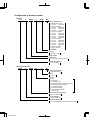
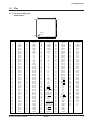
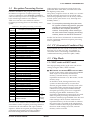
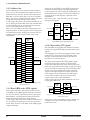
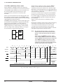
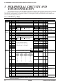
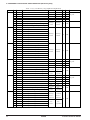
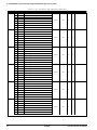
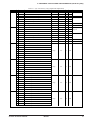
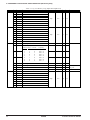
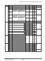
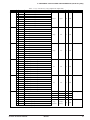
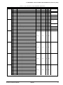
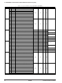
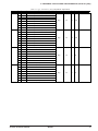
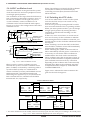
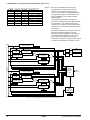
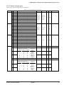
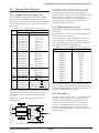
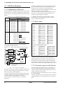
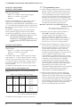
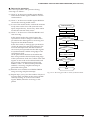
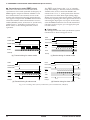
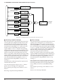
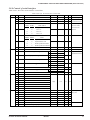
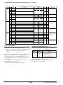
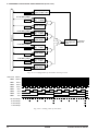
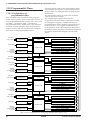
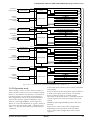
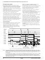
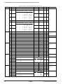
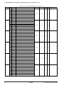
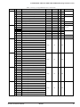
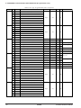
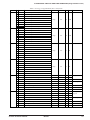
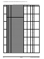
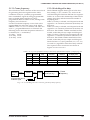
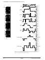
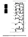
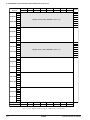
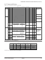
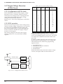
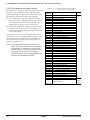
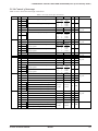
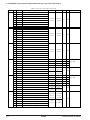
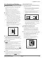
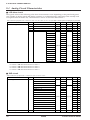
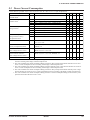
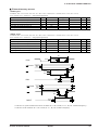
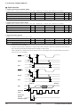
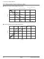
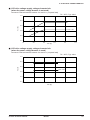
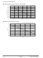
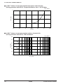
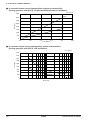
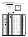
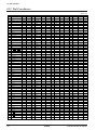
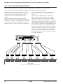
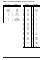
5 PERIPHERAL CIRCUITS AND THEIR OPERATION (Programmable Timer)
[8-bit mode]
[16-bit mode]
8-bit data
Low-order 8-bit data
Timer 0
input clock
Timer 0
Interrupt request
TOUT output
Timer 0
input clock
Timer 0
Timer 1
input clock
Timer 1
Interrupt request
TOUT output
Timer 0
underflow
signal
Timer 1
8-bit data
Interrupt request
TOUT output
High-order 8-bit data
Fig. 5.10.2.1 Counter configuration in 8- and 16-bit mode (example of Timers 0 and 1)
Table 5.10.2.1(a) Control registers in 8-bit mode (example of Timers 0 and 1)
Address Bit Name
00FF30 D7 MODE16_A
D6 PTNREN_A
D5 –
D4 –
D3 PTOUT0
D2 PTRUN0
D1 PSET0
D0 CKSEL0
Function
PTM0–1 8/16-bit mode selection
External clock 0 noise rejecter selection
–
R/W register
PTM0 clock output control
PTM0 Run/Stop control
PTM0 preset
PTM0 input clock selection
00FF31 D7
D6
D5
D4
D3
D2
D1
D0
–
–
–
R/W register
PTM1 clock output control
PTM1 Run/Stop control
PTM1 preset
PTM1 input clock selection
–
–
–
–
PTOUT1
PTRUN1
PSET1
CKSEL1
1
0
16-bit x 1
8-bit x 2
SR
0
0
Enable
Disable
–
–
–
0
1
0
0
On
Off
0
Run
Stop
Preset
No operation 0
External clock Internal clock 0
–
–
–
–
–
–
1
0
On
Off
Run
Stop
Preset
No operation
External clock Internal clock
–
–
–
0
0
0
0
0
R/W
R/W
R/W
Comment
"0" when being read
R/W Reserved register
R/W
R/W
W "0" when being read
R/W
Constantly "0" when
being read
R/W Reserved register
R/W
R/W
W "0" when being read
R/W
Table 5.10.2.1(b) Control registers in 16-bit mode (example of Timers 0 and 1)
Address Bit Name
00FF30 D7 MODE16_A
D6 PTNREN_A
D5 –
D4 –
D3 PTOUT0
D2 PTRUN0
D1 PSET0
D0 CKSEL0
Function
PTM0–1 8/16-bit mode selection
External clock 0 noise rejecter selection
–
R/W register
Invalid (fixed at "0")
PTM0 Run/Stop control
PTM0 preset
PTM0 input clock selection
00FF31 D7
D6
D5
D4
D3
D2
D1
D0
–
–
–
R/W register
PTM1 clock output control
Invalid (fixed at "0")
Invalid (fixed at "0")
Invalid (fixed at "0")
–
–
–
–
PTOUT1
PTRUN1
PSET1
CKSEL1
1
0
16-bit x 1
8-bit x 2
SR
0
0
Enable
Disable
–
–
–
0
1
0
0
Invalid
Fixed at "0"
0
Run
Stop
Preset
No operation 0
External clock Internal clock 0
–
–
–
–
–
–
–
–
–
0
1
0
0
On
Off
0
Invalid
Fixed at "0"
0
Invalid
Fixed at "0"
0
Invalid
Fixed at "0"
R/W
R/W
R/W
Comment
"0" when being read
R/W Reserved register
R/W
R/W
W "0" when being read
R/W
Constantly "0" when
being read
R/W Reserved register
R/W
R/W
W "0" when being read
R/W
Note: The register names contain a timer number (0–7) to identify the timer to which the register belongs.
The following explanation uses "x" instead of the timer number except when it is required. For
example, PTRUNx represents PTRUN0 through PTRUN7. Furthermore, a pair of timers are
described as Timer(L) and Timer(H) in explanations for 16-bit mode.
Timer(L) = Timer 0, Timer 2, Timer 4 or Timer 6
Timer(H) = Timer 1, Timer 3, Timer 5 or Timer 7
This is used for register names.
88
EPSON
S1C88650 TECHNICAL MANUAL