1
APPENDIX A S5U1C88000P1&S5U1C88649P2 MANUAL (Peripheral Circuit Board for S1C88650)
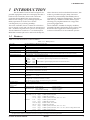
Oscillation circuit
• The OSC1 crystal oscillation frequency is fixed
at 32.768 kHz.
• The OSC1 CR oscillation frequency can be
adjusted in the range of approx. 20 kHz to 500
kHz using the control on the S5U1C88000P1
front panel. Note that the actual IC does not
operate with all of these frequencies; refer to
Chapter 8, "ELECTRICAL CHARACTERISTICS" to select the appropriate operating
frequency.
• The OSC3 crystal oscillation frequency is fixed
at 4.9152 MHz.
• The OSC3 CR oscillation frequency can be
adjusted in the range of approx. 100 kHz to 8
MHz using the control on the S5U1C88000P1
front panel. Note that the actual IC does not
operate with all of these frequencies; refer to
Chapter 8, "ELECTRICAL CHARACTERISTICS" to select the appropriate operating
frequency.
Reset circuit
Keep in mind that the operation sequence from
when the ICE with this board installed is
powered on until the time at which the
program starts running differs from the
sequence of the actual IC. This is because this
board becomes capable of operating as a
debugging system after the user program and
optional data are downloaded.
Internal power supply circuit
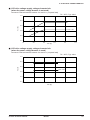
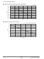
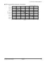
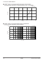
The LCD drive voltage on this board is
different from that on the actual IC.
Size of the Kanji-font ROM
The actual IC contains 896K bytes of Kanji-font
memory (address 010000H to 0EFFFFH). The
memory size implemented in the ICE is 448K
bytes.
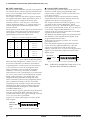
• The S5U1C88000P1&S5U1C88649P2 does not
include the OSC3 ceramic oscillation circuit.
When ceramic oscillation circuit is selected by
mask option, the S5U1C88649P2 uses the onboard crystal oscillation circuit.
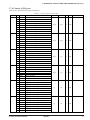
• When using an external clock, adjust the
external clock (amplitude: 3.3 V ±5%, duty:
50% ±10%) and input to the OSC1 or OSC3
terminal with VSS as GND.
• This board can operate normally even when the
CPU clock is switched to OSC3 (CLKCHG = "1")
immediately after the OSC3 oscillation control
circuit is turned on (SOSC3 = "1") without a wait
time inserted. In the actual IC, an oscillation
stability wait time is required before switching
the CPU clock after the OSC3 oscillation is
turned on. Refer to Chapter 8, "ELECTRICAL
CHARACTERISTICS" when setting the appropriate wait time for the actual IC.
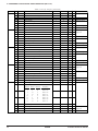
• Use separate instructions to switch the clock
from OSC3 to OSC1 and to turn off the OSC3
oscillation circuit. If executed simultaneously
with a single instruction, these operations,
although good with this board, may not
function properly with the actual IC.
• This board contains oscillation circuits for
OSC1 and OSC3. Keep in mind that even
though the actual IC may not have a resonator
connected to its OSC3, this board can operate
with the OSC3 circuit.
• Because the logic level of the oscillation circuit
is high, the timing at which the oscillation
starts on this board differs from that of
theactual IC.
S1C88650 TECHNICAL MANUAL
Access to undefined address space
If any undefined space in the S1C88650's
internal ROM/RAM or I/O is accessed for
data read or write operations, the read/written
value is indeterminate. Additionally, it is
important to remain aware that the indeterminate state differs between this board and the
actual IC.
Function option
• Input interface level
The actual IC allows selection of the input
interface level either COMS level or CMOS
Schmitt level by a function option. This board
supports CMOS level only and selection of the
function option using Winfog does not affect
the interface level of this board.
(4) Notes on model support
Parameter file
The ROM, RAM and I/O spaces in the ICE with
this board installed are configured when the
debugger on the personal computer starts up
using the parameter file (88650.par) provided for
each model.
The parameter file allows the user to modify its
contents according to the ROM and RAM spaces
actually used. Do not configure areas other than
below when using the IC in single chip maximum mode.
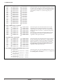
ROM area: 0000H to BFFFH
10000H to EFFFFH
RAM area: D800H to F7FFH
Stack area: D800H to F7FFH
Access disable area
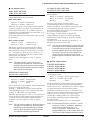
When using this board for development of an
S1C88650 application, be sure not to read and
write from/to I/O memory addresses FF16H
and FF90H to FFADH.
Furthermore, do not change the initial values
when writing to bit D4 of address FF17H, bits D6
and D7 of address FF21H, bit D7 of address
FF22H, and bit D7 of address FF26H.
EPSON
167