1
5 PERIPHERAL CIRCUITS AND THEIR OPERATION (Serial Interface)
S1C88650
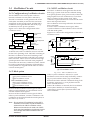
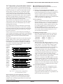
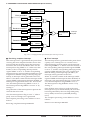
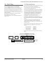
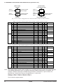
External
serial device
SIN(P10)
Data input
SOUT(P11)
Data output
SCLK(P12)
CLOCK input
Input port(Kxx)
READY output
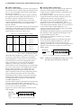
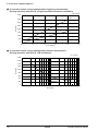
(a) Clock synchronous master mode
S1C88650
External
serial device
SIN(P10)
Data input
SOUT(P11)
Data output
SCLK(P12)
CLOCK output
SRDY(P13)
READY input
(b) Clock synchronous slave mode
S1C88650
External
serial device
SIN(P10)
Data input
SOUT(P11)
Data output
(c) Asynchronous 7-bit/8-bit mode
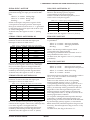
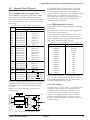
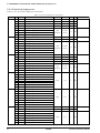
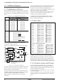
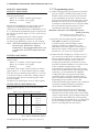
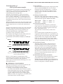
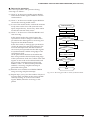
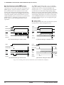
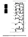
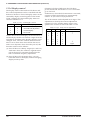
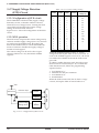
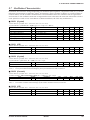
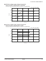
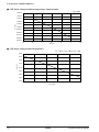
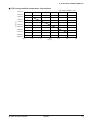
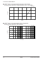
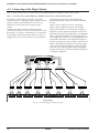
Fig. 5.8.3.1 Connection examples of serial interface I/O terminals
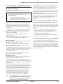
5.8.4 Clock source
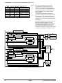
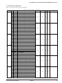
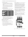
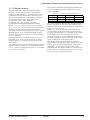
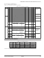
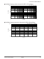
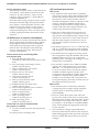
There are four clock sources and selection is made
by setting the two bits of the clock source selection
register SCS0 and SCS1 as shown in table below.
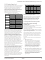
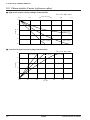
Table 5.8.4.1 Clock source
SCS1
1
SCS0
1
1
0
0
1
0
0
Clock source
Programmable timer
fOSC3 / 4
fOSC3 / 8
fOSC3 / 16
This register setting is invalid in clock synchronous
slave
_________mode and the external clock input from the
SCLK terminal is used.
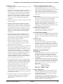
When the "programmable timer" is selected, the
programmable timer 1 underflow signal is divided
by 2 and this signal is used as the clock source.
With respect to the transfer rate setting, see "5.10
Programmable Timer".
At initial reset, the synchronous clock is set to
"fOSC3/16".
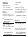
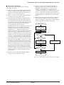
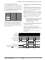
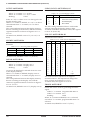
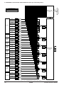
Whichever clock is selected, the signal is further
divided by 16 and then used as the synchronous
clock.
Furthermore, external clock input is used as is for
_________
SCLK in clock synchronous slave mode.
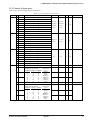
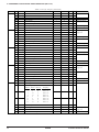
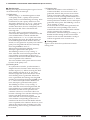
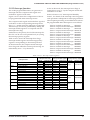
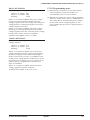
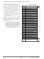
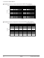
Table 5.8.4.2 shows an examples of transfer rates and
OSC3 oscillation frequencies when the clock source
is set to programmable timer.
When the demultiplied signal of the OSC3 oscillation circuit is made the clock source, it is necessary
to turn the OSC3 oscillation ON, prior to using the
serial interface.
A time interval of several msec to several 10 msec,
from the turning ON of the OSC3 oscillation circuit
to until the oscillation stabilizes, is necessary, due to
the oscillation element that is used. Consequently,
you should allow an adequate waiting time after
turning ON of the OSC3 oscillation, before starting
transmitting/receiving of serial interface. (The
oscillation start time will vary somewhat depending
on the oscillator and on the externally attached parts.
Refer to the oscillation start time example indicated
in Chapter 8, "ELECTRICAL CHARACTERISTICS".)
At initial reset, the OSC3 oscillation circuit is set to
ON status.
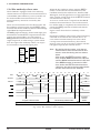
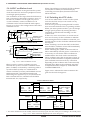
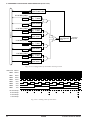
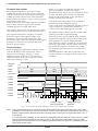
1/4
OSC3
fOSC3
1/8
oscillation
Divider
1/16
circuit
Programmable timer 1
Fig. 5.8.4.1 underflow signal
Division of the synchronous clock
SCLK
Selector
1/16
Selector
Synchronous clock
1/2
(Clock synchronous slave mode)
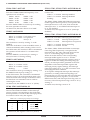
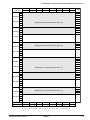
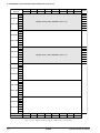
Table 5.8.4.2 OSC3 oscillation frequencies and transfer rates
OSC3 oscillation frequency / Programmable timer settings
Transfer rate
fOSC3 = 2.4756 MHz fOSC3 = 3.0720 MHz fOSC3 = 3.6864 MHz
(bps)
PST1X
RDR1X
PST1X
RDR1X
PST1X
RDR1X
19,200
00H
03H
00H
04H
00H
05H
9,600
00H
07H
00H
09H
00H
0BH
4,800
00H
0FH
00H
13H
00H
17H
2,400
00H
1FH
00H
27H
00H
2FH
1,200
00H
3FH
00H
4FH
00H
5FH
600
00H
7FH
00H
9FH
00H
BFH
300
02H
1FH
03H
09H
01H
BFH
150
02H
3FH
03H
13H
02H
5FH
∗ Since the underflow signal only is used as the clock source, the
CDR1X register value does not affect the transfer rates.
S1C88650 TECHNICAL MANUAL
EPSON
63