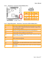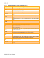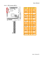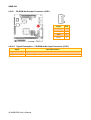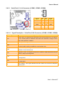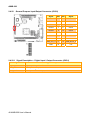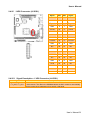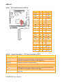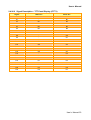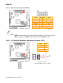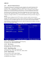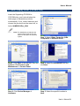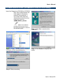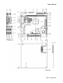
1
ALX-800 Series AMD Geode LX800 @ 09 W with 128K L2 Cache or 64K L1 Cache Mini ITX Main Board with VGA, LVDS, Audio, Dual LAN, CF, PCI, Mini PCI, 4 COM & 4 USB 2.0 User’s Manual 2007 March AIMB-220 FCC Statement THIS DEVICE COMPLIES WITH PART 15 FCC RULES. OPERATION IS SUBJECT TO THE FOLLOWING TWO CONDITIONS: (1) THIS DEVICE MAY NOT CAUSE HARMFUL INTERFERENCE. (2) THIS DEVICE MUST ACCEPT ANY INTERFERENCE RECEIVED INCLUDING INTERFERENCE THAT MAY CAUSE UNDESIRED OPERATION. THIS EQUIPMENT HAS BEEN TESTED AND FOUND TO COMPLY WITH THE LIMITS FOR A CLASS "A" DIGITAL DEVICE, PURSUANT TO PART 15 OF THE FCC RULES. THESE LIMITS ARE DESIGNED TO PROVIDE REASONABLE PROTECTION AGAINST HARMFUL INTERFERENCE WHEN THE EQUIPMENT IS OPERATED IN A COMMERCIAL ENVIRONMENT. THIS EQUIPMENT GENERATES, USES, AND CAN RADIATE RADIO FREQUENCY ENERGY AND, IF NOT INSTATLLED AND USED IN ACCORDANCE WITH THE INSTRUCTION MANUAL, MAY CAUSE HARMFUL INTERFERENCE TO RADIO COMMUNICATIONS. OPERATION OF THIS EQUIPMENT IN A RESIDENTIAL AREA IS LIKELY TO CAUSE HARMFUL INTERFERENCE IN WHICH CASE THE USER WILL BE REQUIRED TO CORRECT THE INTERFERENCE AT HIS OWN EXPENSE. Notice This guide is designed for experienced users to setup the system within the shortest time. For detailed information, please always refer to the electronic user's manual. Copyright Notice Copyright © 2005-2006 Advantech Corp., ALL RIGHTS RESERVED. No part of this document may be reproduced, copied, translated, or transmitted in any form or by any means, electronic or mechanical, for any purpose, without the prior written permission of the original manufacturer. Trademark Acknowledgement Brand and product names are trademarks or registered trademarks of their respective owners. 2 AIMB-220 User’s Manual User’s Manual Disclaimer Advantech Corp. reserves the right to make changes, without notice, to any product, including circuits and/or software described or contained in this manual in order to improve design and/or performance. Advantech Corp. assumes no responsibility or liability for the use of the described product(s), conveys no license or title under any patent, copyright, or masks work rights to these products, and makes no representations or warranties that these products are free from patent, copyright, or mask work right infringement, unless otherwise specified. Applications that are described in this manual are for illustration purposes only. Advantech Corp. makes no representation or warranty that such application will be suitable for the specified use without further testing or modification. Life Support Policy ADVANTECH CORP. PRODUCTS ARE NOT FOR USE AS CRITICAL COMPONENTS IN LIFE SUPPORT DEVICES OR SYSTEMS WITHOUT THE PRIOR WRITTEN APPROVAL OF ADVANTECH CORP.. As used herein: 1. Life support devices or systems are devices or systems which, (a) are intended for surgical implant into body, or (b) support or sustain life and whose failure to perform, when properly used in accordance with instructions for use provided in the labeling, can be reasonably expected to result in significant injury to the user. 2. A critical component is any component of a life support device or system whose failure to perform can be reasonably expected to cause the failure of the life support device or system, or to affect its safety or effectiveness. A Message to the Customer Advantech Customer Services Each and every Advantech product is built to the most exacting specifications to ensure reliable performance in the harsh and demanding conditions typical of industrial environments. Whether your new Advantech device is destined for the laboratory or the factory floor, you can be assured that your product will provide the reliability and ease of operation for which the name Advantech has come to be known. Your satisfaction is our primary concern. Here is a guide to Advantech customer services. To ensure you get the full benefit of our services, please follow the instructions below carefully. User’s Manual 3 AIMB-220 Technical Support We want you to get the maximum performance from your products. So if you run into technical difficulties, we are here to help. For the most frequently asked questions, you can easily find answers in your product documentation. These answers are normally a lot more detailed than the ones we can give over the phone. So please consult the user’s manual first. To receive the latest version of the user’s manual; please visit our Web site at: http://www.Advantech.com.tw/ If you still cannot find the answer, gather all the information or questions that apply to your problem, and with the product close at hand, call your dealer. Our dealers are well trained and ready to give you the support you need to get the most from your Advantech products. In fact, most problems reported are minor and are able to be easily solved over the phone. In addition, free technical support is available from Advantech engineers every business day. We are always ready to give advice on application requirements or specific information on the installation and operation of any of our products. Please do not hesitate to call or e-mail us. Headquarters Advantech Corp. No.1 Alley 20, Lane 26, Rueiguang Road, Neihu District, Taipei 114, Taiwan Tel : +886-2-2792-7818 Fax : +886-2-2794-7306 http://www.Advantech.com.tw E-mail: [email protected] 4 AIMB-220 User’s Manual User’s Manual Product Warranty Advantech warrants to you, the original purchaser, that each of its products will be free from defects in materials and workmanship for two years from the date of purchase. This warranty does not apply to any products which have been repaired or altered by persons other than repair personnel authorized by Advantech, or which have been subject to misuse, abuse, accident or improper installation. Advantech assumes no liability under the terms of this warranty as a consequence of such events. Because of Advantech high quality-control standards and rigorous testing, most of our customers never need to use our repair service. If any of Advantech products is defective, it will be repaired or replaced at no charge during the warranty period. For out-of-warranty repairs, you will be billed according to the cost of replacement materials, service time, and freight. Please consult your dealer for more details. If you think you have a defective product, follow these steps: 1. Collect all the information about the problem encountered. (For example, CPU type and speed, Advantech products / model name, hardware & BIOS revision number, other hardware and software used, etc.) Note anything abnormal and list any on-screen messages you get when the problem occurs. 2. Call your dealer and describe the problem. Please have your manual, product, and any helpful information available. 3. If your product is diagnosed as defective, obtain an RMA (return material authorization) number from your dealer. This allows us to process your good return more quickly. 4. Carefully pack the defective product, a complete Repair and Replacement Order Card and a photocopy proof of purchase date (such as your sales receipt) in a shippable container. A product returned without proof of the purchase date is not eligible for warranty service. 5. Write the RMA number visibly on the outside of the package and ship it prepaid to your dealer. User’s Manual 5 AIMB-220 Contents 1. Getting Started............................................................................................................9 1.1 Safety Precautions ....................................................................................................9 1.2 Packing List...............................................................................................................9 1.3 Document Amendment History ...............................................................................10 1.4 Manual Objectives...................................................................................................11 1.5 System Specifications .............................................................................................12 1.6 Architecture Overview .............................................................................................14 1.6.1 Block Diagram ................................................................................................................................ 14 1.6.2 AMD Geode GX3 & CS5536.......................................................................................................... 15 1.6.3 Realtek ALC203 Audio Codec ....................................................................................................... 19 1.6.4 Ethernet.......................................................................................................................................... 20 1.6.5 Winbond W83627HF-AW LPC Super I/O ...................................................................................... 21 1.6.6 NS DS90C385 LVDS Transmitter .................................................................................................. 21 1.6.7 Fintek F81216D LPC to 4UART..................................................................................................... 22 2. Hardware Configuration...........................................................................................23 2.1 Product Overview....................................................................................................24 2.2 Installation Procedure .............................................................................................25 2.2.1 2.3 2.4 Main Memory.................................................................................................................................. 26 Jumper and Connector List .....................................................................................28 Setting Jumpers & Connectors ...............................................................................30 2.4.1 Clear CMOS (JBAT1)..................................................................................................................... 30 2.4.2 COM1 RS-232/422/485 Select (JP1, JP3)..................................................................................... 30 2.4.3 COM1 Pin 9 Signal Select (JP2) .................................................................................................... 31 2.4.4 CF Master/Slave Mode Select (JP4).............................................................................................. 31 2.4.5 ATX Power Used (JS3V2).............................................................................................................. 32 2.4.6 4/5/8-wire Touch Screen Select (SW1) (Optional)......................................................................... 32 2.4.7 Micro DOC Select (SW2) ............................................................................................................... 33 2.4.8 CPU/Memory Frequency Select (SW3) ......................................................................................... 34 2.4.9 ATX Power Connector (ATXPWR1)............................................................................................... 35 2.4.10 Parallel Port Connector & VGA Connector (CN1) ..................................................................... 36 2.4.11 Serial Port 1 Connector in RS-232 Mode (CN1)........................................................................ 37 2.4.12 Serial Port 1 Connector in RS-422 Mode (CN1)........................................................................ 38 2.4.13 Serial Port 1 Connector in RS-485 Mode (CN1)........................................................................ 39 2.4.14 Audio Connector (CN2).............................................................................................................. 40 2.4.15 RJ-45 Ethernet / USB 3, 4, 1 & 2 Connectors (CN3, CN4) ....................................................... 40 2.4.16 4/5/8-Wire Touch Screen Connector (CN5) (Optional).............................................................. 40 2.4.17 Floppy Connector (FLP1)........................................................................................................... 41 6 AIMB-220 User’s Manual User’s Manual 2.4.18 IDE Connector (IDE_1) .............................................................................................................. 43 2.4.19 LCD Inverter Connector (JBKL1)............................................................................................... 45 2.4.20 CD-ROM Audio Input Connector (JCD1)................................................................................... 46 2.4.21 Serial Port 2, 3 & 4 Connector (JCOM2, JCOM3, JCOM4)....................................................... 47 2.4.22 General Purpose Input/Output Connector (JDIO1) ................................................................... 48 2.4.23 Front Panel Connector (JFP1) ................................................................................................... 49 2.4.24 IrDA Connector (JIR1) ............................................................................................................... 50 2.4.25 LVDS Connector (JLVDS1) ....................................................................................................... 51 2.4.26 TFT Panel Connector (JTFT1)................................................................................................... 52 2.4.27 Micro DOC Connector (JUSB1) ................................................................................................. 54 2.4.28 LCD Backlight Brightness Adjustment Connector (JVR1) ......................................................... 54 3. BIOS Setup................................................................................................................55 3.1 Starting Setup .........................................................................................................56 3.2 Using Setup ............................................................................................................57 3.3 Getting Help ............................................................................................................58 3.4 In Case of Problems................................................................................................58 3.5 Main Menu ..............................................................................................................59 3.5.1 Standard CMOS Features.............................................................................................................. 60 3.5.2 Advanced BIOS Features .............................................................................................................. 62 3.5.3 Advanced Chipset Features........................................................................................................... 66 3.5.4 Integrated Peripherals .................................................................................................................... 68 3.5.5 Power Management Setup............................................................................................................. 70 3.5.6 PnP / PCI Configuration ................................................................................................................. 71 3.5.7 PC Health Status............................................................................................................................ 72 3.5.8 Load Fail-Safe Defaults.................................................................................................................. 72 3.5.9 Load Optimized Defaults ................................................................................................................ 73 3.5.10 Set Supervisor / User Password................................................................................................ 73 3.5.11 Save & Exit Setup ...................................................................................................................... 75 3.5.12 Exit Without Save....................................................................................................................... 75 4. Drivers Installation ...................................................................................................76 4.1 Install Chipset Driver (For AMD GX3) .....................................................................77 4.2 Install Audio Driver (For AMD GX3) ........................................................................79 4.3 Install Display Driver (For AMD GX3)......................................................................81 4.4 Install Ethernet Driver (For Realtek RTL810x, RTL813x Family) ............................83 5. Measurement Drawing .............................................................................................84 Appendix A: AWARD BIOS POST Messages ................................................................86 Overview............................................................................................................................87 Post Beep ..........................................................................................................................87 Error Messages .................................................................................................................87 1. CMOS BATTERY HAS FAILED ......................................................................................................... 87 User’s Manual 7 AIMB-220 2. CMOS CHECKSUM ERROR ............................................................................................................. 87 3. DISK BOOT FAILURE, INSERT SYSTEM DISK AND PRESS ENTER ............................................ 87 4. DISKETTE DRIVES OR TYPES MISMATCH ERROR - RUN SETUP.............................................. 87 5. DISPLAY SWITCH IS SET INCORRECTLY...................................................................................... 88 6. DISPLAY TYPE HAS CHANGED SINCE LAST BOOT ..................................................................... 88 7. EISA Configuration Checksum Error PLEASE RUN EISA CONFIGURATION UTILITY................... 88 8. EISA Configuration Is Not Complete PLEASE RUN EISA CONFIGURATION UTILITY ................... 88 9. ERROR ENCOUNTERED INITIALIZING HARD DRIVE.................................................................... 88 10. ERROR INITIALIZING HARD DISK CONTROLLER ..................................................................... 88 11. FLOPPY DISK CNTRLR ERROR OR NO CNTRLR PRESENT ................................................... 88 12. Invalid EISA Configuration PLEASE RUN EISA CONFIGURATION UTILITY .............................. 89 13. KEYBOARD ERROR OR NO KEYBOARD PRESENT ................................................................. 89 14. Memory Address Error at ... ........................................................................................................... 89 15. Memory parity Error at ................................................................................................................... 89 16. MEMORY SIZE HAS CHANGED SINCE LAST BOOT ................................................................. 89 17. Memory Verify Error at ... ............................................................................................................... 89 18. OFFENDING ADDRESS NOT FOUND ......................................................................................... 89 19. OFFENDING SEGMENT: .............................................................................................................. 89 20. PRESS A KEY TO REBOOT ......................................................................................................... 90 21. PRESS F1 TO DISABLE NMI, F2 TO REBOOT ........................................................................... 90 22. RAM PARITY ERROR - CHECKING FOR SEGMENT ... ............................................................. 90 23. Should Be Empty But EISA Board Found PLEASE RUN EISA CONFIGURATION UTILITY....... 90 24. Should Have EISA Board But Not Found PLEASE RUN EISA CONFIGURATION UTILITY ....... 90 25. Slot Not Empty ............................................................................................................................... 90 26. SYSTEM HALTED, (CTRL-ALT-DEL) TO REBOOT ... ................................................................. 90 27. Wrong Board In Slot PLEASE RUN EISA CONFIGURATION UTILITY........................................ 91 28. FLOPPY DISK(S) fail (80) → Unable to reset floppy subsystem................................................... 91 29. FLOPPY DISK(S) fail (40) → Floppy Type dismatch..................................................................... 91 30. Hard Disk(s) fail (80) → HDD reset failed.................................................................................... 91 31. Hard Disk(s) fail (40) → HDD controller diagnostics failed.......................................................... 91 32. Hard Disk(s) fail (20) → HDD initialization error.......................................................................... 91 33. Hard Disk(s) fail (10) → Unable to recalibrate fixed disk............................................................. 91 34. Hard Disk(s) fail (08) → Sector Verify failed................................................................................ 91 35. Keyboard is locked out - Unlock the key. ....................................................................................... 91 36. Keyboard error or no keyboard present. ........................................................................................ 91 37. Manufacturing POST loop.............................................................................................................. 91 38. BIOS ROM checksum error - System halted. ................................................................................ 91 39. Memory test fail. ............................................................................................................................. 91 40. POST Codes .................................................................................................................................. 92 8 AIMB-220 User’s Manual User’s Manual 1. Getting Started 1.1 Safety Precautions Warning! Always completely disconnect the power cord from your chassis whenever you work with the hardware. Do not make connections while the power is on. Sensitive electronic components can be damaged by sudden power surges. Only experienced electronics personnel should open the PC chassis. Caution! Always ground yourself to remove any static charge before touching the CPU card. Modern electronic devices are very sensitive to static electric charges. As a safety precaution, use a grounding wrist strap at all times. Place all electronic components in a static-dissipative surface or static-shielded bag when they are not in the chassis. 1.2 Packing List Before you begin installing your single board, please make sure that the following materials have been shipped: z 1 x AIMB-220 AMD Geode LX800 Mini ITX Motherboard Board z 1 x Quick Installation Guide z 1 x CD-ROM or DVD-ROM contains the followings: z — User’s Manual (this manual in PDF file) — Ethernet driver and utilities — VGA drivers and utilities — Audio drivers and utilities 1 x Cable set contains the followings: — — — — — — 1 x IDE HDD cable (40-pin, pitch 2.54mm) 1 x FDD cable (34-pin, pitch 2.54mm) 3 x Serial port cable (10-pin, pitch 2.54mm) 1 x I/O Bracket 1 x Startup Manual 1 x Warranty Card User’s Manual 9 AIMB-220 1.3 Document Amendment History Revision st 1 Date March, 2006 Initial Release 10 AIMB-220 User’s Manual Comment User’s Manual 1.4 Manual Objectives This manual describes in detail the Advantech AIMB-220 Single Board. We have tried to include as much information as possible but we have not duplicated information that is provided in the standard IBM Technical References, unless it proved to be necessary to aid in the understanding of this board. We strongly recommend that you study this manual carefully before attempting to interface with AIMB-220 series or change the standard configurations. Whilst all the necessary information is available in this manual we would recommend that unless you are confident, you contact your supplier for guidance. Please be aware that it is possible to create configurations within the CMOS RAM that make booting impossible. If this should happen, clear the CMOS settings, (see the description of the Jumper Settings for details). If you have any suggestions or find any errors concerning this manual and want to inform us of these, please contact our Customer Service department with the relevant details. User’s Manual 11 AIMB-220 1.5 System Specifications System Onboard AMD Geode [email protected] with 128K L2 Cache & 64K L1 CPU Cache CPU BIOS Award 512 KB Flash BIOS System Chipset AMD Geode LX series/CS5536 I/O Chip Winbond W83627HG-AW System Memory One 184-pin DIMM socket supports up to 1GB DDR 266/333 SDRAM SSD One CompactFlash Type I/II socket Watchdog Timer Reset: 1 sec.~255 min. and 1 sec. or 1 min./step H/W Status Monitor Monitoring CPU temperature, voltage Expansion One PCI slot (PCI Rev. 2.2 compliant), One Mini PCI Slot I/O 2 x EIDE (Ultra DMA 100), 1 x FDD, 1 x LPT, 3 x RS-232, MIO 1 x RS-232/422/485, 1 x K/B, 1 x Mouse IrDA 115k bps, IrDA 1.0 compliant USB 4 x USB 2.0 ports DIO 16-bit General Purpose I/O for DI and DO Display Chipset AMD Geode LX800 with integrated graphics engine Display Memory 8/16 MB frame buffer using system memory CRT mode: 1920 x 1440 @ 32 bpp (85 Hz) Resolution LCD mode: 1600 x 1200 @ 32 bpp (60 Hz) VGA/LCD Interface Supports 18/24-bit TFT panel LVDS Single channel 24-bit LVDS Audio Chipset AMD Geode CS5536 AC97 Codec Relteck ALC203 supports 2CH Audio Interface Mic in, Line in, CD Audio in, Line out 12 AIMB-220 User’s Manual User’s Manual Ethernet LAN Dual Realtek RTL8100C Ethernet Interface 100Base-Tx Fast Ethernet compatible Mechanical & Environmental +5 V @ 0.84 A, +12 V @ 0.06 A, +3.3 V @ 0.37 A, 5 Vsb @ 0.02 A (with Power Requirement AMD LX800 433 MHz & 512 MB DDR SDRAM) Power Type ATX Operation Temperature 0~60oC (32~140o F) Operating Humidity 0%~90% relative humidity, non-condensing Size ( L x W ) 6.69" x 6.69" (17 mm x 17 mm) Weight 0.88 lbs (0.4 Kg) User’s Manual 13 AIMB-220 1.6 Architecture Overview 1.6.1 Block Diagram The following block diagram shows the architecture and main components of AIMB-220. The following sections provide detail information about the functions provided onboard. 14 AIMB-220 User’s Manual User’s Manual 1.6.2 AMD Geode GX3 & CS5536 The AMD Geode™ GX3 processors are integrated x86 processors specifically designed to power embedded devices for entertainment, education, and business. Serving the needs of consumers and business professionals alike, it’s an excellent solution for embedded applications, such as thin clients, interactive set-top boxes, single board computers, and mobile computing devices. LX Processor General Features: • • • • • • • • • • • • • • • 0.13 micron process 481-Terminal BGU (Ball Grid Array Cavity Up) with internal heatspreader x86/x87-compatible CPU core Processor frequency: up to 500 MHz Dhrystone 2.1 MIPs: 150 to 450 Split I/D cache/TLB (Translation Look-aside Buffer): 64 KB I-cache/64 KB D-cache 128 KB L2 cache configurable as I-cache, D-cache, or both Efficient pre-fetch and branch prediction Integrated FPU that supports the MMX® and AMD 3DNow!™ instruction sets Fully pipelined single precision FPU hardware with microcode support for higher precisions JTAG interface: ATPG, Full Scan, BIST on all arrays 1149.1 Boundary Scan compliant ICE (in-circuit emulator) interface Reset and clock control Designed for improved software debug methods and performance analysis Power Management: Thermal Design Power (TDP) 2.4W, 1.6W typical @ 500 MHz max power (projected) GeodeLink active hardware power management Hardware support for standard ACPI software power management I/O companion SUSP/SUSPA power controls Lower power I/O Wakeup on SMI/INTR User’s Manual 15 AIMB-220 GeodeLink™ Memory Controller • High bandwidth packetized uni-directional bus for internal peripherals • Standardized protocol to allow variants of products to be developed by adding or removing modules • GeodeLink Control Processor (GLCP) for diagnostics and scan control • Dual GeodeLink Interface Units (GLIUs) for device interconnect GeodeLink™ Memory Controller • Integrated memory controller for low latency to CPU and on-chip peripherals • 64-bit wide DDR SDRAM bus operating frequency: 200 MHz, 400 MT/S • Supports unbuffered DDR DIMMS using up to 1 GB • DRAM technology • Supports up to 2 DIMMS (32 devices max) 2D Graphics Processor • High performance 2D graphics controller • Alpha BLT • Microsoft® Windows® GDI GUI acceleration: Hardware support for all Microsoft RDP codes • Command buffer interface for asynchronous BLTs • Second pattern channel support • Hardware screen rotation Display Controller • Hardware frame buffer compression improves Unified • Memory Architecture (UMA) memory efficiency • CRT resolutions supported: Supports up to 1920x1440x32 bpp at 85 Hz Supports up to 1600x1200x32 bpp at 100 Hz • Supports up to 1600x1200x32 bpp at 60 Hz for TFT • Standard Definition (SD) resolution for Video Output Port (VOP): 720x482 at 59.94 Hz interlaced for NTSC 768x576 at 50 Hz interlaced for PAL • High Definition (HD) resolution for Video Output Port (VOP): Up to 1920x1080 at 30 Hz interlaced (1080i HD) (74.25 MHz) Up to 1280x720 at 60 Hz progressive (720p HD) (74.25 MHz) • Supports down to 7.652 MHz Dot Clock (320x240 QVGA) • Hardware VGA • Hardware supported 48x64 32-bit cursor with alpha blending 16 AIMB-220 User’s Manual User’s Manual Video Processor Supports video scaling, mixing and VOP • Hardware video up/down scalar • Graphics/video alpha blending and color key muxing • Digital VOP (SD and HD) or TFT outputs • Legacy RGB mode • VOP supports SD and HD 480p, 480i, 720p, and 1080i • VESA 1.1, 2.0 and BT.601 24-bit (out only), BT.656 compliant GeodeLink™ PCI Bridge • PCI 2.2 compliant • 3.3V signaling and 3.3V I/Os • 33 to 66 MHz operation • 32-bit interface • Supports virtual PCI headers for GeodeLink devices Video Input Port (VIP) • VESA 1.1 and 2.0 compliant, 8 or 16-bit • Video Blanking Interval (VBI) support • 8 or 16-bit 80 MHz SD or HD capable • Security Block • Serial EEPROM interface for 2K bit unique ID and AES • (Advanced Encryption Standard) hidden key storage • (EEPROM optional inside package) • Electronic Code Book (ECB) or Cipher Block Chaining (CBC)128-bit AES hardware support • True random number generator (TRNG) The AMD Geode™ CS5536 companion device is designed to work with an integrated processor North Bridge component such as the AMD Geode™ LX processor. Together, the Geode LX processor and Geode CS5536 companion device provide a system-level solution well suited for the high-performance and low-power needs of a host of embedded devices including digital set-top boxes, mobile computing devices, thin client applications, and single board computers. The internal architecture uses a single, high-performance modular structure based on GeodeLink™ architecture. This architecture yields high internal speed (over 4 GB/s) data movement and extremely versatile internal power management. The GeodeLink architecture is transparent to application software. Communication with the Geode Geode LX processor is over a 33/66 MHz PCI bus. • User’s Manual 17 AIMB-220 The Geode CS5536 companion device incorporates many I/O functions, including some found in typical superI/O chips, simplifying many system designs. Since the graphics subsystem is entirely contained in the Geode GX3 processor, system interconnect is simplified. The device contains state-of-the-art power management that enables systems, especially battery powered systems, to significantly reduce power consumption. Audio is supported by an internal controller, designed to connect to multiple AC97 compatible codecs. An IR (infrared) port supports all popular IR communication protocols. The IR port is shared with one of two industry-standard serial ports that can reach speeds of 115.2 kbps. An LPC (low pin count) port is provided to facilitate connections to a superI/O should additional expansion, such as a floppy drive, be necessary, and/or to an LPC ROM for the system BIOS. The hard disk controller is compatible to the ATA-6 specification. The bus mastering IDE controller includes support for two ATA-compliant devices on one channel. The CS5536 companion device provides four Universal Serial Bus (USB) 2.0 compliant ports, supporting low speed, full speed, and high speed connections. All four ports are individually automatically associated with either the Open Host Controller Interface (OHCI) or the Enhanced Host Controller Interface (EHCI) depending on the attached device type. A battery-backed real-time clock (RTC) keeps track of time and provides calendar functions. A suite of 82xx devices provides the legacy PC functionality required by most designs, including two PICs (programmable interrupt controllers), one PIT (programmable interval timer) with three channels, and DMA (direct memory access) functions. The CS5536 companion device contains eight MFGPTs (multi-function general purpose timers) that can be used for a variety of functions. A number of GPIOs (general purpose input/outputs) are provided, and are assigned to system functions on power-up (i.e., LPC port). State-of-the-art power management features are attained with the division of the device into two internal power domains. The GPIOs and multi-function timers are distributed into each domain allowing them to act as wakeup sources for the device. The device provides full ACPI (Advanced Configuration Power Interface) compliance and supports industry-standard Wakeup and Sleep modes. For implementation details and suggestions for this device, see the supporting documentation (i.e., application notes, schematics, etc.) on the AMD Alchemy™ and Geode™ Developer Support web site. 18 AIMB-220 User’s Manual User’s Manual 1.6.3 Realtek ALC203 Audio Codec The ALC203 is a 20-bit DAC and 18-bit ADC full-duplex AC'97 2.3 compatible stereo audio CODEC designed for PC multimedia systems, including host/soft audio, and AMR/CNR based designs. The ALC203 incorporates proprietary converter technology to achieve a high SNR (greater than 100 dB), sensing logics for device reporting, and a Universal Audio Jack® for improved user convenience. The ALC203 AC'97 CODEC supports multiple CODEC extensions with independent variable sampling rates and built-in 3D effects. The ALC203 CODEC provides two pairs of stereo outputs with independent volume controls, a mono output, multiple stereo and mono inputs, along with flexible mixing, gain, and mute functions to provide a complete integrated audio solution for PCs. The circuitry of the ALC203 CODEC operates from a 3.3V digital and 3.3V/5V analog power supply with EAPD (External Amplifier Power Down) control for use in notebook and PC applications. The ALC203 integrates a 50mW/20Ohm headset audio amplifier into the CODEC, saving BOM costs. The ALC203 also supports the S/PDIF out function (complies with AC'97 2.3) that offers easy connection of PCs to consumer electronic products, such as AC3 decoders/speakers and mini disk devices. The ALC203 CODEC supports host/soft audio from Intel ICHx chipsets as well as audio controller based VIA/SIS/ALI/AMD/nVIDIA/ATI chipsets. Bundled Windows series drivers (Win98/ME/NT/2000/XP, EAX/Direct Sound 3D/I3DL2/A3D compatible sound effect utilities (supporting Karaoke, 26-kinds of environment sound emulation, 10-band equalizer), HRTF 3D positional audio and Sensaura™ 3D (optional) provide an excellent entertainment package and game experience for PC users. An internal 14.318MHz -> 24.576MHz PLL circuit generates required timing signals, eliminating the need for external crystal, whilst a built-in PCBEEP generator removes the need for an external buzzer. User’s Manual 19 AIMB-220 1.6.4 Ethernet 1.6.4.1 Realtek RTL8100C Ethernet Controller The Realtek RTL8100C(L) is enhanced with an ACPI (Advanced Configuration Power Interface) management function for PCI in order to provide efficient power management for advanced operating systems with OSPM (Operating System Directed Power Management). It also supports remote wake-up (including AMD Magic Packet™ and Microsoft® Wake-up frame) to increase cost-efficiency in network maintenance and management. • 128-pin PQFP/LQFP (PQFP package pin-to-pin compatible with Realtek RTL8110S-32 Single-Chip Gigabit Ethernet Controller) • Supports PCI/mini-PCI interfaces • Integrates Fast Ethernet MAC, physical chip, and transceiver onto a single chip • 10Mbps and 100Mbps operation supporting N-way auto-negotiation • Supports 25MHz Crystal or 25MHz OSC as the internal clock source • Complies with PC99/PC2001 standards • Supports ACPI power management • Provides PCI bus master data transfer • Provides PCI memory space or I/O space mapped data transfer • Supports PCI clock speed of 16.75MHz-40MHz • Advanced power saving mode • Supports Wake-on-LAN and remote wake-up (AMD Magic Packet™, Link Change, and Microsoft® Wake-up frame) • Half/Full duplex capability • Supports Full Duplex Flow Control (IEEE 802.3x) • Provides interface to 93C46 EEPROM to store resource configuration and ID parameters • Provides PCI clock run pin • Provides LED pins for network operation status indication • 2.5/3.3V power supply with 5V tolerant I/Os • 0.25µm CMOS process 1.6.4.2 LAN (RJ-45) Port This port allows Gigabit connection to a Local Area Network (LAN) through a network hub. Refer to the table below for the LAN port LED indications. 20 AIMB-220 User’s Manual User’s Manual 1.6.5 Winbond W83627HF-AW LPC Super I/O The Winbond W83627F/HF is made to fully comply with Microsoft PC98 and PC99 Hardware Design Guide. Moreover, W83627F/HF is made to meet the specification of PC98/PC99’s requirement in the power management: ACPI and DPM (Device Power Management). Super I/O chip provides features as the following: • • • • • • • • Meet LPC Spec. 1.0 Support LDRQ# (LPC DMA), SERIRQ (serial IRQ) Include all features of Winbond I/O W83977TF and W83977EF Integrate Hardware Monitor functions Compliant with Microsoft PC98/PC99 Hardware Design Guide. Support DPM (Device Power Management), ACPI Programmable configuration settings Single 24 or 48 MHz clock input 1.6.6 NS DS90C385 LVDS Transmitter The DS90C385 transmitter converts 28 bits of LVCMOS/LVTTL data into four LVDS (Low Voltage Differential Signaling) data streams. A phase-locked transmit clock is transmitted in parallel with the data streams over a fifth LVDS link. Every cycle of the transmit clock 28 bits of input data are sampled and transmitted. At a transmit clock frequency of 85 MHz, 24 bits of RGB data and 3 bits of LCD timing and control data (FPLINE, FPFRAME, DRDY) are transmitted at a rate of 595 Mbps per LVDS data channel. Using a 85 MHz clock, the data throughput is 297.5 Mbytes/sec. Also available is the DS90C365 that converts 21 bits of LVCMOS/LVTTL data into three LVDS (Low Voltage Differential Signaling) data streams. Both transmitters can be programmed for Rising edge strobe or Falling edge strobe through a dedicated pin. A Rising edge or Falling edge strobe transmitter will interoperate with a Falling edge strobe Receiver (DS90CF386/DS90CF366) without any translation logic. User’s Manual 21 AIMB-220 1.6.7 Fintek F81216D LPC to 4UART The F81216D mainly provides 3 pure UART ports and one UART+ IR port through LPC. Each UART includes 16-byte send/receive FIFO, a programmable baud rate generator, complete modem control capability and an interrupt system. One watch dog timer is provided for system controlling and the time interval can be programmed by register or hardware power on setting pin. One clock 24/48MHz input is necessary, and default is 24MHz. Powered by 3.3V voltage, the F81216D is in the small 48pin LQFP package (7mm x 7mm). • • • • • • • • Supports LPC interface Totally provides 4 UART (16550 asynchronous) ports 3 Pure UART 1 UART+IR 1 watch dog timer with WDTOUT# signal 1 frequency input 24/48MHz Powered by 3Vcc 48-LQFP(7mm x 7mm) 22 AIMB-220 User’s Manual User’s Manual 2. Hardware Configuration User’s Manual 23 AIMB-220 2.1 Product Overview 24 AIMB-220 User’s Manual User’s Manual 2.2 Installation Procedure This chapter explains you the instructions of how to setup your system. 1. Turn off the power supply. 2. Insert the DIMM module (be careful with the orientation). 3. Insert all external cables for hard disk, floppy, keyboard, mouse, USB etc. except for flat panel. A CRT monitor must be connected in order to change CMOS settings to support flat panel. 4. Connect power supply to the board via the ATXPWR. 5. Turn on the power. 6. Enter the BIOS setup by pressing the delete key during boot up. Use the “LOAD BIOS DEFAULTS” feature. The Integrated Peripheral Setup and the Standard CMOS Setup Window must be entered and configured correctly to match the particular system configuration. 7. If TFT panel display is to be utilized, make sure the panel voltage is correctly set before connecting the display cable and turning on the power. User’s Manual 25 AIMB-220 2.2.1 Main Memory AIMB-220 provides one 184-pin DIMM socket to support DDR SDRAM. The total maximum memory size is 1GB. DIMM1 Make sure to unplug the power supply before adding or removing DIMMs or other system components. Failure to do so may cause severe damage to both the board and the components. 26 AIMB-220 User’s Manual User’s Manual • • • • Locate the DIMM slot on the board. Hold two edges of the DIMM module carefully. Keep away of touching its connectors. Align the notch key on the module with the rib on the slot. Firmly press the modules into the slot automatically snaps into the mounting notch. Do not force the DIMM module in with extra force as the DIMM module only fit in one direction. • To remove the DIMM module, push the two ejector tabs on the slot outward simultaneously, and then pull out the DIMM module. Note: (1) Please do not change any DDR SDRAM parameter in BIOS setup to increase your system’s performance without acquiring technical information in advance. (2) Static electricity can damage the electronic components of the computer or optional boards. Before starting these procedures, ensure that you are discharged of static electricity by touching a grounded metal object briefly. User’s Manual 27 AIMB-220 2.3 Jumper and Connector List You can configure your board to match the needs of your application by setting jumpers. A jumper is the simplest kind of electric switch. It consists of two metal pins and a small metal clip (often protected by a plastic cover) that slides over the pins to connect them. To “close” a jumper you connect the pins with the clip. To “open” a jumper you remove the clip. Sometimes a jumper will have three pins, labeled 1, 2, and 3. In this case, you would connect either two pins. The jumper settings are schematically depicted in this manual as follows: A pair of needle-nose pliers may be helpful when working with jumpers. Connectors on the board are linked to external devices such as hard disk drives, a keyboard, or floppy drives. In addition, the board has a number of jumpers that allow you to configure your system to suit your application. If you have any doubts about the best hardware configuration for your application, contact your local distributor or sales representative before you make any changes. The following tables list the function of each of the board's jumpers and connectors. Jumpers Label Function Note JBAT1 Clear CMOS 3 x 1 header, pitch 2.54mm JP1, JP3 COM1 RS-232/422/485 select 3 x 2 header, pitch 2.54mm 4 x 3 header, pitch 2.54mm JP2 COM1 pin 9 signal select 3 x 2 header, pitch 2.54mm JP4 CF master/slave mode select 2 x 1 header, pitch 2.54mm JS3V2 ATX power used 2 x 2 header, pitch 2.54mm SW1 4/5/8-wire touch screen select (Optional) Switch SW2 Micro DOC select Switch SW3 CPU/Memory frequency select Switch 28 AIMB-220 User’s Manual User’s Manual Connectors Label Function Note ATXPWR1 ATX Power connector CN1 Parallel port connector Serial port 1 connector VGA connector D-sub 25-pin, female D-sub 9-pin, male D-sub 15-pin, female CN2 Audio connector Phone Jack X 3 CN3 RJ-45 Ethernet / USB 2 & 3 connector CN4 RJ-45 Ethernet / USB 0 & 1 connector CN5 4/5/8-wire touch screen connector (Optional) DIMM1 184-pin DDR SDRAM DIMM socket FAN1 System fan connector 1 3 x 1 wafer, pitch 2.54mm FAN2 System fan connector 2 3 x 1 wafer, pitch 2.54mm FLP1 Floppy connector 17 x 2 header, pitch 2.54mm IDE1 Primary IDE connector 20 x 2 header, pitch 2.54mm JBKL1 LCD inverter connector 5 x 1 wafer, pitch 2.0mm JCD1 CD-ROM audio input connector 4 x 1 wafer, pitch 2.0mm JCOM2 Serial port 2 connector 5 x 2 header, pitch 2.54mm JCOM3 Serial port 3 connector 5 x 2 header, pitch 2.54mm JCOM4 Serial port 4 connector 5 x 2 header, pitch 2.54mm JDIO1 General purpose input/output connector 10 x 2 header, pitch 2.54mm JFP1 Front panel connector 8 x 2 header, pitch 2.54mm JIR1 IrDA connector 5 x 1 header, pitch 2.54mm JLVDS1 LVDS connector HIROSE DF13-40DP-1.25V JTFT1 TFT panel connector HIROSE DF13-40DP-1.25V JUSB1 Micro DOC connector 5 x 2 header, pitch 2.54mm JVR1 LCD backlight brightness adjustment connector 3 x 1 header, pitch 2.54mm KB_MS1 PS/2 Keyboard & mouse connector 6-pin Mini-DIN x 2 MPCI1 Mini PCI slot PCI1 PCI slot SN1 CompactFlash card connector 9 x 1 wafer, pitch 2.0 mm User’s Manual 29 AIMB-220 2.4 Setting Jumpers & Connectors 2.4.1 Clear CMOS (JBAT1) Protect* Clear CMOS * Default 2.4.2 COM1 RS-232/422/485 Select (JP1, JP3) (JP1) RS-232* (JP3) RS-232* RS-422 RS-422 RS-485 RS-485 JP1 JP3 * Default 30 AIMB-220 User’s Manual User’s Manual 2.4.3 COM1 Pin 9 Signal Select (JP2) +5V Ring* +12V * Default 2.4.4 CF Master/Slave Mode Select (JP4) Master Slave* * Default User’s Manual 31 AIMB-220 2.4.5 ATX Power Used (JS3V2) Note: JS3V2 is set for ATX power used, please do not remove the jumpers of 1-2, 3-4 while using. 2.4.6 4/5/8-wire Touch Screen Select (SW1) (Optional) * Default 32 AIMB-220 User’s Manual Wire BIT1 BIT2 * 4, 8 OFF ON 5 ON OFF User’s Manual 2.4.7 Micro DOC Select (SW2) Default* Micro DOC * Default Note: JUSB1 (Micro DOC connector) uses the same port with the USB connector 3 (the bottom deck of CN3), and SW2 is to select the USB connector 3 or Micro DOC function. The default setting of SW2 is for USB connector 3 used. User’s Manual 33 AIMB-220 2.4.8 CPU/Memory Frequency Select (SW3) * Default LX800 (CPU @ 500 MHz) 266 MHz* Memory 34 AIMB-220 User’s Manual 333 MHz Memory 400 MHz Memory User’s Manual 2.4.9 ATX Power Connector (ATXPWR1) Signal PIN PIN Signal +12V 10 20 +5V VCCSB 9 19 +5V PWROK 8 18 -5V GND 7 17 GND +5V 6 16 GND GND 5 15 GND +5V 4 14 PS_ON GND 3 13 GND +3.3V 2 12 -12V +3.3V 1 11 +3.3V User’s Manual 35 AIMB-220 2.4.10 Parallel Port Connector & VGA Connector (CN1) Port Parallel Parallel VGA Description Connects a parallel printer, a scanner, or other devices. For pointing devices or other COM serial devices VGA COM Signal RED PIN Signal 6 GND 1 11 7 GREEN 2 GND 12 8 BLUE 3 13 4 5 HSYNC VCC 14 10 GND DAT GND 9 NC NC VSYNC GND 15 DCK 2.4.10.1 Signal Description – VGA Connector (CN1) Signal Signal Description HSYNC CRT horizontal synchronisation output. VSYNC CRT vertical synchronisation output. DCK DAT RED GREEN BLUE Display Data Channel Clock. Used as clock signal to/from monitors with DDC interface. Display Data Channel Data. Used as data signal to/from monitors with DDC interface. Analog output carrying the red colour signal to the CRT. For 75 Ω cable impedance. Analog output carrying the green colour signal to the CRT. For 75 Ω cable impedance. Analog output carrying the blue colour signal to the CRT. For 75 Ω cable impedance. 36 AIMB-220 User’s Manual User’s Manual 2.4.11 Serial Port 1 Connector in RS-232 Mode (CN1) Signal PIN PIN Signal DCD 1 2 RxD TxD 3 4 DTR GND 5 6 DSR RTS 7 8 CTS RI/+5V/+12V 9 10 NC 2.4.11.1 Signal Description – Serial Port 1 Connector in RS-232 Mode (CN1) Signal Signal Description Serial output. This signal sends serial data to the communication link. The signal is TxD set to a marking state on hardware reset when the transmitter is empty or when loop mode operation is initiated. RxD DTR DSR RTS CTS DCD RI Serial input. This signal receives serial data from the communication link. Data Terminal Ready. This signal indicates to the modem or data set that the on-board UART is ready to establish a communication link. Data Set Ready. This signal indicates that the modem or data set is ready to establish a communication link. Request To Send. This signal indicates to the modem or data set that the on-board UART is ready to exchange data. Clear To Send. This signal indicates that the modem or data set is ready to exchange data. Data Carrier Detect. This signal indicates that the modem or data set has detected the data carrier. Ring Indicator. This signal indicates that the modem has received a telephone ringing signal. User’s Manual 37 AIMB-220 2.4.12 Serial Port 1 Connector in RS-422 Mode (CN1) Signal PIN PIN Signal TxD- 1 2 RxD+ TxD+ 3 4 RxD- GND 5 6 NC NC 7 8 NC NC 9 10 NC 2.4.12.1 Signal Description – Serial Port 1 Connector in RS-422 Mode (CN1) Signal Signal Description Serial output. This differential signal pair sends serial data to the communication TxD+/- link. Data is transferred from Serial Port 2 Transmit Buffer Register to the communication link, if the RTS register of the Serial Port 2 is set to LOW. Serial input. This differential signal pair receives serial data from the RxD+/- communication link. Received data is available in Serial Port 2 Receiver Buffer Register. 38 AIMB-220 User’s Manual User’s Manual 2.4.13 Serial Port 1 Connector in RS-485 Mode (CN1) Signal PIN PIN Signal DATA- 1 2 NC DATA+ 3 4 NC GND 5 6 NC NC 7 8 NC NC 9 10 NC 2.4.13.1 Signal Description – Serial Port 1 Connector in RS-485 Mode (CN1) Signal Signal Description This differential signal pair sends and receives serial data to the communication DATA+/- link. The mode of this differential signal pair is controlled through the RTS register of Serial Port 2. Set the RTS register of the Serial Port 2 to LOW for transmitting, HIGH for receiving. Do not select a mode different from the one used by the connected peripheral, as this may damage CPU board and/or peripheral. The transmitter drivers in the port are short circuit protected by a thermal protection circuit. The circuit disables the drivers when the die temperature reaches 150 °C. RS-422 mode is typically used in point to point communication. Data and control signal pairs should be terminated in the receiver end with a resistor matching the cable impedance (typical 100-120 Ω). The resistors could be placed in the connector housing. RS-485 mode is typically used in multi drop applications, where more than 2 units are communicating. The data and control signal pairs should be terminated in each end of the communication line with a resistor matching the cable impedance (typical 100-120 Ω). Stubs to substations should be avoided. User’s Manual 39 AIMB-220 2.4.14 Audio Connector (CN2) Port Audio-In Description Connects a tape player or Audio-In other audio sources. Audio-Out Connects a headphone or a Audio-Out Microphone 2.4.15 Microphone Connects a microphone. RJ-45 Ethernet / USB 3, 4, 1 & 2 Connectors (CN3, CN4) Port CN3 Description Allows connection to a Local RJ-45 Area Network (LAN) through CN4 a network hub. For connecting USB port 3, USB 2.0 2.4.16 speaker. 4 (CN3), 1, 2 (CN4) 4/5/8-Wire Touch Screen Connector (CN5) (Optional) 40 AIMB-220 User’s Manual PIN 4-Wire 5-Wire 8-Wire 1 NA NA Right Sense 2 NA NA Left Sense 3 NA NA Bottom Sense 4 NA Sense Top Sense 5 Right LR Right Excite 6 Left LL Left Excite 7 Bottom UR Bottom Excite 8 Top UL Top Excite 9 GND GND GND User’s Manual 2.4.17 Floppy Connector (FLP1) Signal PIN PIN Signal GND 1 2 REDWC GND 3 4 NC GND 5 6 NC GND 7 8 INDEX GND 9 10 MOTSA GND 11 12 DRVSB GND 13 14 DRVSA GND 15 16 MOTEB GND 17 18 DIR GND 19 20 STEP GND 21 22 WDATA GND 23 24 WGATE GND 25 26 TK00 GND 27 28 WPT GND 29 30 RDATA GND 31 32 SIDE1 GND 33 34 DSKCHG User’s Manual 41 AIMB-220 2.4.17.1 Signal Description – Floppy Connector (FLP1) Signal RDATA WDATA WGATE MOATSA MOTEB DRVSA DRVSB SIDE1 Signal Description The read data input signal from the FDD. Write data. This logic low open drain writes pre-compensation serial data to the selected FDD. An open drain output. Write enable. An open drain output. Motor A On. When set to 0, this pin enables disk drive 0. This is an open drain output. Motor B On. When set to 0, this pin enables disk drive 1. This is an open drain output. Drive Select A. When set to 0, this pin enables disk drive A. This is an open drain output. Drive Select B. When set to 0, this pin enables disk drive B. This is an open drain output. This output signal selects side of the disk in the selected drive. Direction of the head step motor. An open drain output DIR Logic 1 = outward motion Logic 0 = inward motion STEP REDWC TK00 INDEX WPT DSKCHG Step output pulses. This active low open drain output produces a pulse to move the head to another track. This output indicates whether a low drive density (250/300kbps at low level) or a high drive density (500/1000kbps at high level) has been selected. Track 0. This Schmitt-triggered input from the disk drive is active low when the head is positioned over the outermost track. This Schmitt-triggered input from the disk drive is active low when the head is positioned over the beginning of a track marked by an index hole. Write protected. This active low Schmitt input from the disk drive indicates that the diskette is write-protected. Diskette change. This signal is active low at power on and whenever the diskette is removed. 42 AIMB-220 User’s Manual User’s Manual 2.4.18 IDE Connector (IDE_1) Signal PIN PIN Signal RESET# 1 2 GND PDD7 3 4 PDD8 PDD6 5 6 PDD9 PDD5 7 8 PDD10 PDD4 9 10 PDD11 PDD3 11 12 PDD12 PDD2 13 14 PDD13 PDD1 15 16 PDD14 PDD0 17 18 PDD15 GND 19 20 NC PDREQ 21 22 GND PDIOW# 23 24 GND PDIOR# 25 26 GND PIORDY 27 28 GND PDDACK# 29 30 GND IRQ14 31 32 NC PDA1 33 34 PATADET PDA0 35 36 PDA2 PDCS1# 37 38 PDCS3# IDEACTP# 39 40 GND User’s Manual 43 AIMB-220 2.4.18.1 Signal Description – IDE Connector (IDE_1) The IDE interface supports PIO modes 0 to 4 and Bus Master IDE. Data transfer rates up to 100 MB/Sec is possible. Signal DA [2:0] DCS1#, DCS3# D [15:0] IOR# IOW# IORDY Signal Description IDE Address Bits. These address bits are used to access a register or data port in a device on the IDE bus. IDE Chip Selects. The chip select signals are used to select the command block registers in an IDE device. DCS1# selects the primary hard disk. IDE Data Lines. D [15:0] transfers data to/from the IDE devices. IDE I/O Read. Signal is asserted on read accesses to the corresponding IDE port addresses. IDE I/O Write. Each signal is asserted on write accesses to corresponding the IDE port addresses. When deasserted, these signals extend the transfer cycle of any host register access when the device is not ready to respond to the data transfer request. RESET# IDE Reset. This signal resets all the devices that are attached to the IDE interface. IRQ14 Interrupt line from hard disk. Connected directly to PC-AT bus. DREQ DACK# DACT# PATADET, SATADET The DREQ is used to request a DMA transfer from the South Bridge. The direction of the transfers is determined by the IOR#/IOW# signals. DMA Acknowledge. The DACK# acknowledges the DREQ request to initiate DMA transfers. Signal from hard disk indicating hard disk activity. The signal level depends on the hard disk type, normally active low. The signal is routed directly to the LED1. Primary/Secondary IDE detected. 44 AIMB-220 User’s Manual User’s Manual 2.4.19 LCD Inverter Connector (JBKL1) Signal PIN +12V 1 GND 2 ENBKL 3 VR 4 +5V 5 Note: For inverters with adjustable Backlight function, it is possible to control the LCD brightness through the VR signal controlled by JVR1. Please see the JVR1 section for detailed circuitry information. 2.4.19.1 Signal Description – LCD Inverter Connector (JBKL1) Signal Signal Description VR Vadj = 0.75V ~ 4.25V (Recommended: 4.7KΩ, >1/16W) ENBKL LCD backlight ON/OFF control signal User’s Manual 45 AIMB-220 2.4.20 CD-ROM Audio Input Connector (JCD1) Signal PIN NC 1 CD_L 2 GND 3 CD_R 4 2.4.20.1 Signal Description – CD-ROM Audio Input Connector (JCD1) Signal Signal Description CD_R Right CD-IN signal CD_L Left CD-IN signal 46 AIMB-220 User’s Manual User’s Manual 2.4.21 Serial Port 2, 3 & 4 Connector (JCOM2, JCOM3, JCOM4) JCOM3 JCOM4 JCOM2 Signal PIN PIN Signal DCD 1 2 RxD TxD 3 4 DTR GND 5 6 DSR RTS 7 8 CTS RI 9 10 NC 2.4.21.1 Signal Description – Serial Port 2/3/4 Connector (JCOM2, JCOM3, JCOM4) Signal Signal Description Serial output. This signal sends serial data to the communication link. The signal is TxD set to a marking state on hardware reset when the transmitter is empty or when loop mode operation is initiated. RxD DTR DSR RTS CTS DCD RI Serial input. This signal receives serial data from the communication link. Data Terminal Ready. This signal indicates to the modem or data set that the on-board UART is ready to establish a communication link. Data Set Ready. This signal indicates that the modem or data set is ready to establish a communication link. Request To Send. This signal indicates to the modem or data set that the on-board UART is ready to exchange data. Clear To Send. This signal indicates that the modem or data set is ready to exchange data. Data Carrier Detect. This signal indicates that the modem or data set has detected the data carrier. Ring Indicator. This signal indicates that the modem has received a telephone ringing signal. User’s Manual 47 AIMB-220 2.4.22 General Purpose Input/Output Connector (JDIO1) Signal PIN PIN Signal GPO20 1 2 GPI10 GPO21 3 4 GPI11 GPO22 5 6 GPI12 GPO23 7 8 GPI13 GPO30 9 10 GPI14 GPO31 11 12 GPI15 GPO32 13 14 GPI16 GPO33 15 16 GPI17 SMB_CLK_S 17 18 SMB_DATA_S GND 19 20 +5V 2.4.22.1 Signal Description – Digital Input / Output Connector (JDIO1) Signal Signal Description DI [0:17] Digital Input/Output Data Bit 0 to Bit 17 SMB_CLK Data input for I2C input, 5V tolerant SMB_DATA Data input for I2C serial input, 5V tolerant 48 AIMB-220 User’s Manual User’s Manual 2.4.23 Front Panel Connector (JFP1) Signal PIN PIN Signal RESET 1 2 SYS_LED+ GND 3 4 SYS_LED- HDD_LED+ 5 6 PWR_LED+ HDD_LED- 7 8 PWR_LED- GND 9 10 SUS_LED+ PWR_BUT 11 12 SUS_LED- SUS_BUT 13 14 SPK+ GND 15 16 SPK- 2.4.23.1 Signal Description – Front Panel Connecter (JFP1) PIN No. Description 1, 3 Reset SW 2, 4 System LED 5, 7 HDD LED 6, 8 Power-On LED 9, 11 Power SW 10, 12 Suspend LED 13, 15 Suspend SW 14, 16 Speaker User’s Manual 49 AIMB-220 2.4.24 IrDA Connector (JIR1) Signal PIN +5V 1 NC 2 IRRX 3 GND 4 IRTX 5 2.4.24.1 Signal Description – IrDA Connecter (JIR1) Signal Signal Description IRRX Infrared Receiver input IRTX Infrared Transmitter output 50 AIMB-220 User’s Manual User’s Manual 2.4.25 LVDS Connector (JLVDS1) Signal PIN PIN Signal +5V 2 1 +3.3V +5V 4 3 2 +3.3V 2 I C_DAT 6 5 I C_CLK GND 8 7 GND Txout0 10 9 Txout1 Txout0# 12 11 Txout1# GND 14 13 GND Txout2 16 15 Txout3 Txout2# 18 17 Txout3# GND 20 19 GND NC 22 21 NC NC 24 23 NC GND 26 25 GND NC 28 27 NC NC 30 29 NC GND 32 31 GND Txclk 34 33 NC Txclk# 36 35 NC GND 38 37 GND +12V 40 39 +12V 2.4.25.1 Signal Description – LVDS Connector (JLVDS1) Signal Description 2 I2C_DAT, I2C_CLK I C interface for panel parameter EEPROM. This EERPOM is mounted on the LVDS receiver. The data in the EEPROM allows the EXT module to automatically set the proper timing parameters for a specific LCD panel. User’s Manual 51 AIMB-220 2.4.26 TFT Panel Connector (JTFT1) Signal PIN PIN Signal +5V 2 1 +5V GND 4 3 GND +3.3V 6 5 +3.3V GND 8 7 NC P1 10 9 P0 P3 12 11 P2 P5 14 13 P4 P7 16 15 P6 P9 18 17 P8 P11 20 19 P10 P13 22 21 P12 P15 24 23 P14 P17 26 25 P16 P19 28 27 P18 P21 30 29 P20 P23 32 31 P22 GND 34 33 GND FLM 36 35 SHFCLK LP 38 37 M NC 40 39 ENBKL 2.4.26.1 Signal Description – TFT Panel Connector (JTFT1) Signal Description P [0:23] Flat panel data output for 18/24 bit TFT flat panels. Refer to table below for configurations for various panel types. The flat panel data and control outputs are all on-board controlled for secure power-on/off sequencing SHFCLK Shift Clock. Pixel clock for flat panel data LP Flat panel equivalent of HSYNC (horizontal synchronization) FLM Flat panel equivalent of VSYNC (vertical synchronization) M Multipurpose signal, function depends on panel type. May be used as AC drive control signal or as BLANK# or Display Enable signal ENBKL Enable backlight signal. This signal is controlled as a part of the panel power sequencing 52 AIMB-220 User’s Manual User’s Manual 2.4.26.2 Signal Description – TFT Panel Display (JTFT1) Signal 18-bit TFT 24-bit TFT P0 - B0 P1 - B1 P2 B0 B2 P3 B1 B3 P4 B2 B4 P5 B3 B5 P6 B4 B6 P7 B5 B7 P8 - G0 P9 - G1 P10 G0 G2 P11 G1 G3 P12 G2 G4 P13 G3 G5 P14 G4 G6 P15 G5 G7 P16 - R0 P17 - R1 P18 R0 R2 P19 R1 R3 P20 R2 R4 P21 R3 R5 P22 R4 R6 P23 R5 R7 User’s Manual 53 AIMB-220 2.4.27 Micro DOC Connector (JUSB1) Signal PIN PIN Signal +5V 1 2 NC ISUSB3- 3 4 NC ISUSB3+ 5 6 NC GND 7 8 NC NC 9 10 NC Note: JUSB1 uses the same port with the USB connector 3 (the bottom deck of CN3), so please set SW2 to Micro DOC mode if JUSB1 is used. 2.4.28 LCD Backlight Brightness Adjustment Connector (JVR1) JVR1 Signal PIN +5V 1 VR 2 GND 3 VCC 1 JBKL1 pin 4 2 3 Variation Resistor (Recommended: 4.7KΩ, >1/16W) 54 AIMB-220 User’s Manual User’s Manual 3. BIOS Setup User’s Manual 55 AIMB-220 3.1 Starting Setup The AwardBIOS™ is immediately activated when you first power on the computer. The BIOS reads the system information contained in the CMOS and begins the process of checking out the system and configuring it. When it finishes, the BIOS will seek an operating system on one of the disks and then launch and turn control over to the operating system. While the BIOS is in control, the Setup program can be activated in one of two ways: By pressing <Del> immediately after switching the system on, or By pressing the <Del> key when the following message appears briefly at the bottom of the screen during the POST (Power On Self Test). Press DEL to enter SETUP If the message disappears before you respond and you still wish to enter Setup, restart the system to try again by turning it OFF then ON or pressing the "RESET" button on the system case. You may also restart by simultaneously pressing <Ctrl>, <Alt>, and <Delete> keys. If you do not press the keys at the correct time and the system does not boot, an error message will be displayed and you will again be asked to. Press F1 to Continue, DEL to enter SETUP 56 AIMB-220 User’s Manual User’s Manual 3.2 Using Setup In general, you use the arrow keys to highlight items, press <Enter> to select, use the PageUp and PageDown keys to change entries, press <F1> for help and press <Esc> to quit. The following table provides more detail about how to navigate in the Setup program using the keyboard. Button ↑ Description Move to previous item ↓ Move to next item ← Move to the item in the left hand → PgUp key Move to the item in the right hand Main Menu -- Quit and not save changes into CMOS Status Page Setup Menu and Option Page Setup Menu -- Exit current page and return to Main Menu Increase the numeric value or make changes PgDn key Decrease the numeric value or make changes + key Increase the numeric value or make changes - key Decrease the numeric value or make changes F1 key General help, only for Status Page Setup Menu and Option Page Setup Menu (Shift) F2 key Change color from total 16 colors. F2 to select color forward, (Shift) F2 to select color backward F3 key Calendar, only for Status Page Setup Menu F4 key Reserved F5 key Restore the previous CMOS value from CMOS, only for Option Page Setup Menu F6 key Load the default CMOS value from BIOS default table, only for Option Page Setup Menu F7 key Load the default F8 key Reserved F9 key Reserved F10 key Save all the CMOS changes, only for Main Menu Esc key • Navigating Through The Menu Bar Use the left and right arrow keys to choose the menu you want to be in. Note: Some of the navigation keys differ from one screen to another. User’s Manual 57 AIMB-220 • To Display a Sub Menu Use the arrow keys to move the cursor to the sub menu you want. Then press <Enter>. A “¾” pointer marks all sub menus. 3.3 Getting Help Press F1 to pop up a small help window that describes the appropriate keys to use and the possible selections for the highlighted item. To exit the Help Window press <Esc> or the F1 key again. 3.4 In Case of Problems If, after making and saving system changes with Setup, you discover that your computer no longer is able to boot, the AwardBIOS™ supports an override to the CMOS settings which resets your system to its defaults. The best advice is to only alter settings which you thoroughly understand. To this end, we strongly recommend that you avoid making any changes to the chipset defaults. These defaults have been carefully chosen by both Award and your systems manufacturer to provide the absolute maximum performance and reliability. Even a seemingly small change to the chipset setup has the potential for causing you to use the override. 58 AIMB-220 User’s Manual User’s Manual 3.5 Main Menu Once you enter the AwardBIOS™ CMOS Setup Utility, the Main Menu will appear on the screen. The Main Menu allows you to select from several setup functions and two exit choices. Use the arrow keys to select among the items and press <Enter> to accept and enter the sub-menu. Note that a brief description of each highlighted selection appears at the bottom of the screen. Note: The BIOS setup screens shown in this chapter are for reference purposes only, and may not exactly match what you see on your screen. Visit the Advantech website (www.Advantech.com.tw) to download the latest product and BIOS information. User’s Manual 59 AIMB-220 3.5.1 Standard CMOS Features The items in Standard CMOS Setup Menu are divided into few categories. Each category includes no, one or more than one setup items. Use the arrow keys to highlight the item and then use the <PgUp> or <PgDn> keys to select the value you want in each item. 3.5.1.1 Main Menu Selection This reference table shows the selections that you may make on the Main Menu. Item Time IDE Primary Master IDE Primary Slave Options HH : MM : SS Options are in 3.5.1.2 Drive A Drive B Video Halt On 60 AIMB-220 User’s Manual None 360K, 5.25 in 1.2M, 5.25 in 720K, 3.5 in 1.44M, 3.5 in 2.88M, 3.5 in EGA/VGA CGA 40 CGA 80 MONO All Errors No Errors All, but Keyboard All, but Diskette All, but Disk/Key Description Set the system time Press <Enter> to enter the sub menu of detailed options Select the type of floppy disk drive installed in your system Select the default video device Select the situation in which you want the BIOS to stop the POST process and notify you User’s Manual 3.5.1.2 IDE Adapter Setup The IDE adapters control the hard disk drive. Use a separate sub menu to configure each hard disk drive. The below Figure will shows the IDE primary master sub menu. Item Options IDE HDD Auto-detection Press Enter IDE Primary Master IDE Primary Slave, None Auto Manual Description Press Enter to auto-detect the HDD on this channel. If detection is successful, it fills the remaining fields on this menu. Selecting ‘manual’ lets you set the remaining fields on this screen. Selects the type of fixed disk. "User Type" will let you select the number of cylinders, heads, etc. Note: PRECOMP=65535 means NONE ! Choose the access mode for this hard disk CHS LBA Access Mode Large Auto The following options are selectable only if the ‘IDE Channel …’ item is set to ‘Manual’ Min = 0 Set the number of cylinders for this Cylinder Max = 65535 hard disk. Min = 0 Head Set the number of read/write heads Max = 255 Min = 0 **** Warning: Setting a value of 65535 Precomp Max = 65535 means no hard disk Min = 0 Landing zone **** Max = 65535 Min = 0 Sector Number of sectors per track Max = 255 User’s Manual 61 AIMB-220 3.5.2 Advanced BIOS Features This section allows you to configure your system for basic operation. You have the opportunity to select the system’s default speed, boot-up sequence, keyboard operation, shadowing and security. 3.5.2.1 Virus Warning Allows you to choose the VIRUS Warning feature for IDE Hard Disk boot sector protection. If this function is enabled and someone attempt to write data into this area, BIOS will show a warning message on screen and alarm beep. Item Enabled Disabled Description Activates automatically when the system boots up causing a warning message to appear when anything attempts to access the boot sector or hard disk partition table. No warning message will appear when anything attempts to access the boot sector or hard disk partition table. 3.5.2.2 CPU Internal Cache This category speeds up memory access. However, it depends on CPU/chipset design. The default value is en able. Item Enabled Disabled Description Enable cache Disable cache 3.5.2.3 Quick Power On Self Test This category speeds up Power On Self Test (POST) after you power up the computer. If it is set to Enable, BIOS will shorten or skip some check items during POST. Item Enabled Disabled Description Enable quick POST Normal POST 62 AIMB-220 User’s Manual User’s Manual 3.5.2.4 First/Second/Third/Other Boot Device The BIOS attempts to load the operating system from the devices in the sequence selected in these items. Item Floppy LS120 HDD-0~1 SCSI CDROM ZIP100 USB-FDD USB-ZIP USB-CDROM USB-HDD LAN Disabled Description Floppy Device LS120 Device Hard Disk Device 0~1 SCSI Device CDROM Device ZIP-100 Device USB Floppy Device USB ZIP Device USB CDROM Device USB Hard Disk Network Device Disabled any boot device 3.5.2.5 Swap Floppy Drive While system has two floppy drivers installed, this item will be affected. This function is to assign physical drive B to logical drive A. Item Enabled Disabled Description Assign physical drive B to logical drive A No change 3.5.2.6 Boot Up Floppy Seek Select whether the system seeks for a floppy driver every time the system boots. Item Enabled Disabled Description Seek for a floppy driver Skip driver seeking 3.5.2.7 Boot Up NumLock Status Select power on state for NumLock. Item On Off Description Enable NumLock Disable NumLock 3.5.2.8 Gate A20 Option Select if chipset or keyboard controller should control Gate A20. Item Normal Fast Description A pin in the keyboard controller controls Gate A20 Lets chipset control Gate A20 3.5.2.9 Typematic Rate Setting Key strokes repeat at a rate determined by the keyboard controller. When enabled, the typematic rate and typematic delay can be selected. Item Enabled Disabled Description Enable typematic rate/delay setting Disable typematic rate/delay setting User’s Manual 63 AIMB-220 3.5.2.10 Security Option Select whether the password is required every time the system boots or only when you enter setup. Item System Setup Description The system will not boot and access to Setup will be denied if the correct password is not entered at the prompt. The system will boot, but access to Setup will be denied if the correct password is not entered at the prompt. Note: To disable security, select PASSWORD SETTING at Main Menu and then you will be asked to enter password. Do not type anything and just press <Enter>, it will disable security. Once the security is disabled, the system will boot and you can enter Setup freely. 3.5.2.11 OS Select for DRAM > 64MB Select the operating system that is running with greater than 64MB of RAM on the system. Item Non-OS2 OS2 Description Disable OS for over 64 MB DRAM Enable OS for over 64 MB DRAM 3.5.2.12 Full Screen LOGO Show If the BIOS had the full screen logo in it, this item could allow enable/ disable the full screen logo show on display. Item Enable Disable Description Enable full screen logo show Disable full screen logo show 3.5.2.13 Small Logo (EPA) Show This item allows you enabled/disabled the small EPA logo show on screen at the POST step. Item Enabled Disabled Description EPA Logo show is enabled EPA Logo show is disabled 64 AIMB-220 User’s Manual User’s Manual 3.5.2.14 Onboard Lan Boot ROM This item allows to boot over the network when system POST and shorten the booting time by set disabled Item Enabled Disabled Description Enable Onboard LAN boot. Disabled Onboard LAN boot. User’s Manual 65 AIMB-220 3.5.3 Advanced Chipset Features This section allows you to configure the system based on the specific features of the installed chipset. This chipset manages bus speeds and access to system memory resources, such as DRAM and the external cache. It also coordinates communications between the conventional ISA bus and the PCI bus. It must be stated that these items should never need to be altered. The default settings have been chosen because they provide the best operating conditions for your system. The only time you might consider making any changes would be if you discovered that data was being lost while using your system. The first chipset settings deal with CPU access to dynamic random access memory (DRAM). The default timings have been carefully chosen and should only be altered if data is being lost. Such a scenario might well occur if your system had mixed speed DRAM chips installed so that greater delays may be required to preserve the integrity of the data held in the slower memory chips. 3.5.3.1 CPU Frequency This item allows to select CPU/Memory/PCI frequency. The choices: Auto, 200/333/400/433/500 3.5.3.2 CAS Latency This item allows to select CAS Latency. The choices: Auto, 1.5, 2.0, 2.5, 3.0, 3.5. 3.5.3.3 Video Memory Size This item allows to select video memory size. The choices: None , 8 M, 16M, 32 M, 64 M, 128 M, 254 M. 3.5.3.4 Output display This item allows to select output display. The choices: Flat Panel, CRT, Panel & CRT. 66 AIMB-220 User’s Manual User’s Manual 3.5.3.5 Flat Panel Configuration Item Options Flat Panel Type TFT Resolution Data Bus Type Refresh Rate HSYNC Polarity VSYNC Polarity Active SHFCLK Active Period LP Active Period Description This item allows to select the flat panel type. 320x240, 640x480, 800x600, This item allows to select the 1024x768, 1152x864, resolution. 1280x1024, 1600x1200 This item allows to select the data bus 9-24 bits, 1ppc type This refresh rate is only the number of 60Hz, 65Hz, 70Hz, time the image is being refreshed on 72Hz, 75Hz, 85Hz the monitor screen. High, Low Select polarity of HSYNC signals. Set the polarity of VSYNC signals High, Low active. Active only, Shift clock or pixel clock for the flat Free running panel data. Active running Latch Pulse is the line pulse or latch Free running pulse for the flat panel data. 3.5.3.6 Onboard Audio This item allows you to enable the onboard audio function. The choices: Enabled, Disabled. User’s Manual 67 AIMB-220 3.5.4 Integrated Peripherals Use this menu to specify your settings for integrated peripherals. Item On-Chip IDE Channel 1 Options Enabled Disabled Master Drive PIO Mode Slave Drive PIO Mode Auto Mode 0 Mode 1 Mode 2 Mode 3 Mode 4 IDE Primary Master UDMA IDE Primary Slave UDMA Auto Disabled IDE DMA Transfer IDE HDD Block Mode 68 AIMB-220 User’s Manual Description This item allows to enable On-chip IDE channel. The IDE PIO (Programmed Input/Output) fields let you set a PIO mode (0-4) for each of the four IDE devices that the onboard IDE interface supports. Modes 0 through 4 provide successively increased performance. In Auto mode, the system automatically determines the best mode for each device. Ultra DMA implementation is possible only if your IDE hard drive supports it and the operating environment includes a DMA driver (Windows 95 OSR2 or a third-party IDE bus master driver). If the hard drive and the system software both support Ultra DMA, select Auto to enable BIOS support. Enabled Disabled This feature allows you to enable or disable DMA (Direct Memory Access) support for all IDE devices. If you disable this BIOS feature, the BIOS will disable DMA transfers for all IDE drives. They will revert to PIO mode transfers. If you enable this BIOS feature, the BIOS will enable DMA transfers for all IDE drives. The proper DMA mode will be detected at boot-up. If the drive does not support DMA transfers, then it will use PIO mode instead. Enabled Disabled Block mode is also called block transfer, multiple commands, or multiple sector read/write. If the IDE hard drive supports block mode (most new drives do), select Enabled for automatic detection of the optimal number of block read/writes per sector the drive can support. User’s Manual Item Options Onboard FDC Controller Enabled Disabled Onboard Serial Port 1 Onboard Serial Port 2 Disable 3F8/IRQ4 2F8/IRQ3 3E8/IRQ4 2E8/IRQ3 Select an address and corresponding interrupt for the first and second serial ports. UART Mode Select IrDA ASKIR Normal Select UART2 mode as standard serial port or IR port. RxD , TxD Active Hi,Hi Hi,Lo Lo,Hi Lo,Lo This item allows you to determine the active of RxD, TxD level. IR Transmission Delay Enabled Disabled UR2 Duplex Mode Half Full Use IR Pins RxD2,TxD2 IR-Rx2Tx2 Onboard Parallel Port Disabled 378/IRQ7 278/IRQ5 3BC/IRQ7 Parallel Port Mode EPP Mode Select ECP Mode Use DMA Watch Dog Timer Select Onboard Serial Port 3 Onboard Serial Port 4 SPP EPP ECP ECP+EPP Normal EPP1.9 EPP1.7 1 3 Description Select Enabled if your system has a floppy disk controller (FDC) installed on the system board and you wish to use it. If you are not going to use FDC or the system has no floppy drive, select Disabled in this field. This item allows you to enable/disable the IR Transmission Delay. Select the value required by the IR device connected to the IR port. Full-duplex mode permits simultaneous two-direction transmission. Half-duplex mode permits transmission in one direction only at a time. This item allows you to determine the pin definition. Select a matching address and interrupt for the physical parallel (printer) port. Select an operating mode for the onboard parallel port. Select Compatible or Extended unless you are certain both your hardware and software support EPP or ECP mode. Select EPP port type 1.7 or 1.9. Select a DMA channel for the port. Disabled, This option will determine watch dog timer 10, 20, 30, 40 Sec. 1, 2, 4 Min. Disable Select an address and corresponding interrupt 3F8/2F8/3E8/2E8 for the third and fourth serial ports. IRQ5/IRQ7/IRQ10/IRQ11 User’s Manual 69 AIMB-220 3.5.5 Power Management Setup The Power Management Setup allows you to configure you system to most effectively save energy while operating in a manner consistent with your own style of computer use. 3.5.5.1 ACPI Suspend Type This item will set which ACPI suspend type will be used. The choice: S1(POS), S3(STR). 3.5.5.2 Power Management This category allows you to select the type (or degree) of power saving. The choices: Disabled, Legacy, APM, ACPI. 3.5.5.3 MODEM Use IRQ This determines the IRQ in which the MODEM can use. The choices: NA, 3, 4, 5, 7, 9, 10, 11. 3.5.5.4 Soft-Off by PWR-BTTN Pressing the power button for more than 4 seconds forces the system to enter the Soft-Off state when the system has “hung”.(Only could working on ATX Power supply) The choices: Delay 4 Sec, Instant-Off. 70 AIMB-220 User’s Manual User’s Manual 3.5.6 PnP / PCI Configuration This section describes configuring the PCI bus system. PCI, or Personal Computer Interconnect, is a system which allows I/O devices to operate at speeds nearing the speed the CPU itself uses when communicating with its own special components. This section covers some very technical items and it is strongly recommended that only experienced users should make any changes to the default settings. 3.5.6.1 PNP OS Installed The operation system environment is Plug-and-Play aware sets “YES” The choices: Yes, No. 3.5.6.2 Init Display First This item allows you to decide to active whether PCI Slot or AGP first. The choices: PCI Slot, Onboard. 3.5.6.3 Reset Configuration Data Normally, you leave this field Disabled. Select Enabled to reset Extended System Configuration Data (ESCD) when you exit Setup if you have installed a new add-on and the system reconfiguration has caused such a serious conflict that the operating system cannot boot. The choices: Enabled, Disabled. 3.5.6.4 Resources Controlled By The Award Plug and Play BIOS has the capacity to automatically configure all of the boot and Plug and Play compatible devices. However, this capability means absolutely nothing unless you are using a Plug and Play operating system such as Windows®95. If you set this field to “manual” choose specific resources by going into each of the sub menu that follows this field (a sub menu is preceded by a “¾”). The choices: Auto(ESCD), Manual. User’s Manual 71 AIMB-220 3.5.6.5 PCI/VGA Palette Snoop This item is to set non-standard VGA display adapters such as graphics accelerators or MPEG video cards showing colors properly. The choices: Enabled, Disabled. 3.5.7 PC Health Status This section shows the status of your CPU, Fan & System. 3.5.8 Load Fail-Safe Defaults Use this menu to load the BIOS default values for the minimal/stable performance for your system to operate. Press <Y> to load the BIOS default values for the most stable, minimal-performance system operations. 72 AIMB-220 User’s Manual User’s Manual 3.5.9 Load Optimized Defaults Use this menu to load the BIOS default values that are factory settings for optimal performance system operations. While Award has designed the custom BIOS to maximize performance, the factory has the right to change these defaults to meet their needs. Press <Y> to load the default values setting for optimal performance system operations. 3.5.10 Set Supervisor / User Password You can set either supervisor or user password, or both of them. Supervisor Password: able to enter/change the options of setup menus. User’s Manual 73 AIMB-220 User Password: able to enter but no right to change the options of setup menus. Type the password, up to eight characters in length, and press <Enter>. The password typed now will clear any previously entered password from CMOS memory. You will be asked to confirm the password. Type the password again and press <Enter>. You may also press <Esc> to abort the selection and not enter a password. To disable a password, just press <Enter> when you are prompted to enter the password. A message will confirm the password will be disabled. Once the password is disabled, the system will boot and you can enter Setup freely. PASSWORD DISABLED. When a password has been enabled, you will be prompted to enter it every time you try to enter Setup. This prevents an unauthorized person from changing any part of your system configuration. Additionally, when a password is enabled, you can also require the BIOS to request a password every time your system is rebooted. This would prevent unauthorized use of your computer. You determine when the password is required within the BIOS Features Setup Menu and its Security option (see Section 3). If the Security option is set to “System”, the password will be required both at boot and at entry to Setup. If set to “Setup”, prompting only occurs when trying to enter Setup 74 AIMB-220 User’s Manual User’s Manual 3.5.11 Save & Exit Setup Save CMOS value changes to CMOS and exit setup. Enter <Y> to store the selection made in the menus in CMOS, a special section in memory that stays on after turning the system off. The BIOS configures the system according to the Setup selection stored in CMOS when boot the computer next time. The system is restarted after saving the values. 3.5.12 Exit Without Save Abandon all CMOS value changes and exit setup, and the system is restarted after exiting. User’s Manual 75 AIMB-220 4. Drivers Installation Note: Installation procedures and screen shots in this section are for your reference and may not be exactly the same as shown on your screen. 76 AIMB-220 User’s Manual User’s Manual 4.1 Install Chipset Driver (For AMD GX3) Insert the Supporting CD-ROM to CD-ROM drive, and it should show the index page of Advantech’s products automatically. If not, locate Index.htm and choose the product from the menu left, or link to \AIMB-220\Drv_AMD GX3 Note: The installation procedures and screen shots in this section are based on Windows XP operation system. Step 3. Select Entertainment… to Reinstall Driver. Step1. Click Start of the task bar, then the System of Performance and Maintenance in Control Panel. Step 4. Select the Advanced item and click Next. Step 2. Click Device Manager of Hardware. Step 5. Select the specific location to Next. User’s Manual 77 AIMB-220 Step6. The setup will install automatically. Step7. Click Finish to complete the setup. 78 AIMB-220 User’s Manual User’s Manual 4.2 Install Audio Driver (For AMD GX3) Insert the Supporting CD-ROM to CD-ROM drive, and it should show the index page of Advantech’s products automatically. If not, locate Index.htm and choose the product from the menu left, or link to \AIMB-220\Drv_Audio. Note: The installation procedures and screen shots in this section are based on Windows XP operation system. Step 3. Select Multimedia Audio Controller to Reinstall Driver. Step1. Click Start of the task bar, then the System of Performance and Maintenance in Control Panel. Step 4. Select the Advanced item and click Next. Step 2. Click Device Manager of Hardware. Step 5. Select the specific location to Next. User’s Manual 79 AIMB-220 Step6. Click Continue Anyway to run the installation. Step7. Click Finish to complete the setup. 80 AIMB-220 User’s Manual User’s Manual 4.3 Install Display Driver (For AMD GX3) Insert the Supporting CD-ROM to CD-ROM drive, and it should show the index page of Advantech products automatically. If not, locate Index.htm and choose the product from the menu left, or link to \AIMB-220\Drv_VGA. Note: The installation procedures and screen shots in this section are based on Windows XP operation system. Step 3. Select Video Controller (VGA Compatible to Reinstall Driver. Step1. Click Start of the task bar, then the System of Performance and Maintenance in Control Panel. Step 4. Select the Advanced item and click Next. Step 2. Click Device Manager of Hardware. Step 5. Select the specific location to Next. User’s Manual 81 AIMB-220 Step6. Click Continue Anyway to run the installation. Step7. Click Finish to complete the setup. 82 AIMB-220 User’s Manual User’s Manual 4.4 Install Ethernet Driver (For Realtek RTL810x, RTL813x Family) Insert the Supporting CD-ROM to CD-ROM drive, and it should show the index page of Advantech products automatically. If not, locate Index.htm and choose the product from the menu left, or link to \AIMB-220\Drv_Netwo Note: The installation procedures and screen shots in this section are based on Windows XP operation system. Step 1. Locate 「\Driver_Network\Realtek\ RTL810x_813X Family\Setup.exe」. Step 3. Click Yes to continue the installation. Step 4. Click Finish to complete the setup. Step 2. Setup executing. User’s Manual 83 AIMB-220 5. Measurement Drawing 84 AIMB-220 User’s Manual User’s Manual (Unit: mm) User’s Manual 85 AIMB-220 Appendix A: AWARD BIOS POST Messages 86 AIMB-220 User’s Manual User’s Manual Overview During the Power On Self-Test (POST), if the BIOS detects an error requiring you to do something to fix, it will either sound a beep code or display a message. If a message is displayed, it will be accompanied by: PRESS F1 TO CONTINUE OR PRESS DEL TO ENTER SETUP Post Beep Currently there are two kinds of beep codes in BIOS. This code indicates that a video error has occurred and the BIOS cannot initialize the video screen to display any additional information. This beep code consists of a single long beep followed by two short beeps. The other code indicates that your DRAM error has occurred. This beep code consists of a single long beep repeatedly. Error Messages The following messages are examples of messages including errors detected by the BIOS during POST and a description of what they mean and/or what you may do to correct the error. 1. CMOS BATTERY HAS FAILED CMOS battery is no longer functional. It should be replaced. 2. CMOS CHECKSUM ERROR Checksum of CMOS is incorrect. This can indicate that CMOS has become corrupt. This error may have been caused by a weak battery. Check the battery and replace if necessary. 3. DISK BOOT FAILURE, INSERT SYSTEM DISK AND PRESS ENTER No boot device was found. This could mean that either a boot drive was not detected or the drive does not contain proper system boot files. Insert a system disk into Drive A: and press <Enter>. If you assumed the system would boot from the hard drive, make sure the controller is inserted correctly and all cables are properly attached. Also be sure the disk is formatted as a boot device. Then reboot the system. 4. DISKETTE DRIVES OR TYPES MISMATCH ERROR - RUN SETUP Type of diskette drive installed in the system is different from the CMOS definition. Run Setup to reconfigure the drive type correctly. User’s Manual 87 AIMB-220 5. DISPLAY SWITCH IS SET INCORRECTLY Display switch on the motherboard can be set to either monochrome or color. This indicates the switch is set to a different setting than indicated in Setup. Determine which setting is correct, and then either turn off the system and change the jumper, or enter Setup and change the VIDEO selection. 6. DISPLAY TYPE HAS CHANGED SINCE LAST BOOT Since last powering off the system, the display adapter has been changed. You must configure the system for the new display type. 7. EISA Configuration Checksum Error PLEASE RUN EISA CONFIGURATION UTILITY The EISA non-volatile RAM checksum is incorrect or cannot correctly read the EISA slot. This can indicate either the EISA non-volatile memory has become corrupt or the slot has been configured incorrectly. Also be sure the card is installed firmly in the slot. 8. EISA Configuration Is Not Complete PLEASE RUN EISA CONFIGURATION UTILITY The slot configuration information stored in the EISA non-volatile memory is incomplete. Note: When either of these errors appears, the system will boot in ISA mode, which allows you to run the EISA Configuration Utility. 9. ERROR ENCOUNTERED INITIALIZING HARD DRIVE Hard drive cannot be initialized. Be sure the adapter is installed correctly and all cables are correctly and firmly attached. Also be sure the correct hard drive type is selected in Setup. 10. ERROR INITIALIZING HARD DISK CONTROLLER Cannot initialize controller. Make sure the cord is correctly and firmly installed in the bus. Be sure the correct hard drive type is selected in Setup. Also check to see if any jumper needs to be set correctly on the hard drive. 11. FLOPPY DISK CNTRLR ERROR OR NO CNTRLR PRESENT Cannot find or initialize the floppy drive controller. Make sure the controller is installed correctly and firmly. If there are no floppy drives installed, be sure the Diskette Drive selection in Setup is set to NONE. 88 AIMB-220 User’s Manual User’s Manual 12. Invalid EISA Configuration PLEASE RUN EISA CONFIGURATION UTILITY The non-volatile memory containing EISA configuration information was programmed incorrectly or has become corrupt. Re-run EISA configuration utility to correctly program the memory. Note: When either of these errors appears, the system will boot in ISA mode, which allows you to run the EISA Configuration Utility. 13. KEYBOARD ERROR OR NO KEYBOARD PRESENT Cannot initialize the keyboard. Make sure the keyboard is attached correctly and no keys are being pressed during the boot. If you are purposely configuring the system without a keyboard, set the error halt condition in Setup to HALT ON ALL, BUT KEYBOARD. This will cause the BIOS to ignore the missing keyboard and continue the boot. 14. Memory Address Error at ... Indicates a memory address error at a specific location. You can use this location along with the memory map for your system to find and replace the bad memory chips. 15. Memory parity Error at ... Indicates a memory parity error at a specific location. You can use this location along with the memory map for your system to find and replace the bad memory chips. 16. MEMORY SIZE HAS CHANGED SINCE LAST BOOT Memory has been added or removed since the last boot. In EISA mode use Configuration Utility to reconfigure the memory configuration. In ISA mode enter Setup and enter the new memory size in the memory fields. 17. Memory Verify Error at ... Indicates an error verifying a value already written to memory. Use the location along with your system's memory map to locate the bad chip. 18. OFFENDING ADDRESS NOT FOUND This message is used in conjunction with the I/O CHANNEL CHECK and RAM PARITY ERROR messages when the segment that has caused the problem cannot be isolated. 19. OFFENDING SEGMENT: This message is used in conjunction with the I/O CHANNEL CHECK and RAM PARITY ERROR messages when the segment that has caused the problem has been isolated. User’s Manual 89 AIMB-220 20. PRESS A KEY TO REBOOT This will be displayed at the bottom screen when an error occurs that requires you to reboot. Press any key and the system will reboot. 21. PRESS F1 TO DISABLE NMI, F2 TO REBOOT When BIOS detects a Non-maskable Interrupt condition during boot, this will allow you to disable the NMI and continue to boot, or you can reboot the system with the NMI enabled. 22. RAM PARITY ERROR - CHECKING FOR SEGMENT ... Indicates a parity error in Random Access Memory. 23. Should Be Empty But EISA Board Found PLEASE RUN EISA CONFIGURATION UTILITY A valid board ID was found in a slot that was configured as having no board ID. Note: When either of these errors appears, the system will boot in ISA mode, which allows you to run the EISA Configuration Utility. 24. Should Have EISA Board But Not Found PLEASE RUN EISA CONFIGURATION UTILITY The board installed is not responding to the ID request, or no board ID has been found in the indicated slot. Note: When either of these errors appears, the system will boot in ISA mode, which allows you to run the EISA Configuration Utility. 25. Slot Not Empty Indicates that a slot designated as empty by the EISA Configuration Utility actually contains a board. Note: When either of these errors appears, the system will boot in ISA mode, which allows you to run the EISA Configuration Utility. 26. SYSTEM HALTED, (CTRL-ALT-DEL) TO REBOOT ... Indicates the present boot attempt has been aborted and the system must be rebooted. Press and hold down the CTRL and ALT keys and press DEL. 90 AIMB-220 User’s Manual User’s Manual 27. Wrong Board In Slot PLEASE RUN EISA CONFIGURATION UTILITY The board ID does not match the ID stored in the EISA non-volatile memory. Note: When either of these errors appears, the system will boot in ISA mode, which allows you to run the EISA Configuration Utility. 28. FLOPPY DISK(S) fail (80) → Unable to reset floppy subsystem. 29. FLOPPY DISK(S) fail (40) → Floppy Type dismatch. 30. Hard Disk(s) fail (80) → HDD reset failed. 31. Hard Disk(s) fail (40) → HDD controller diagnostics failed. 32. Hard Disk(s) fail (20) → HDD initialization error. 33. Hard Disk(s) fail (10) → Unable to recalibrate fixed disk. 34. Hard Disk(s) fail (08) → Sector Verify failed. 35. Keyboard is locked out - Unlock the key. BIOS detect the keyboard is locked. P17 of keyboard controller is pulled low. 36. Keyboard error or no keyboard present. Cannot initialize the keyboard. Make sure the keyboard is attached correctly and no keys are being pressed during the boot. 37. Manufacturing POST loop. System will repeat POST procedure infinitely while the P15 of keyboard controller is pull low. This is also used for M/B burn in test. 38. BIOS ROM checksum error - System halted. The checksum of ROM address F0000H-FFFFFH is bad. 39. Memory test fail. BIOS reports the memory test fail if the onboard memory is tested error. User’s Manual 91 AIMB-220 40. POST Codes Please take reference to Phoenix-Award website for the latest post codes. http://www.phoenix.com/en/Customer+Services/BIOS/AwardBIOS/Award+Error+Codes.ht m 40.1 Normal POST Code Note: EISA POST codes are typically output to port address 300h. ISA POST codes are output to port address 80h. Code (hex) Name Description C0 Turn Off Chipset and OEM Specific-Cache control cache CPU test Processor Status (1FLAGS) Verification. Tests the following processor status flags: Carry, zero, sign, overflow, the BIOS sets each flag, verifies They are set, then turns each flag off and verifies it is off. Read/Write/Verify all CPU registers except SS, SP, and BP with data pattern FF and 00. RAM must be periodically refreshed to keep the memory from decaying. This function ensures that the memory refresh function is working properly. C1 Memory Presence First block memory detect OEM Specific-Test to size on-board memory. Early chip set initialization Memory presence test OEM chip set routines clear low 64K of memory Test first 64K memory. C2 Early Memory OEM Specific- Board Initialization Initialization C3 Extend Memory DRAM OEM Specific- Turn on extended memory Initialization select Cyrix CPU initialization, Cache initialization Special Display OEM Specific- Display/Video Switch handling so that switch Handling handling display switch errors never occurs C5 Early Shadow OEM specific- Early shadow enable for fast boot C6 Cache presence test External cache size detection CF CMOS Check CMOS checkup B0 Spurious If interrupt occurs in protected mode. B1 Unclaimed NMI If unmasked NMI occurs, display Press F1 to disable NMI, F2 C4 reboot. BF Program Chip Set To program chipset from defaults values E1-EF Setup Pages E1- Page 1, E2 - Page 2, etc. 1 Force load Default to Chipset defaults program chipset 2 Reserved 92 AIMB-220 User’s Manual User’s Manual Code (hex) Name Description 3 Early Superio Init Early Initialized the super IO 4 Reserved 5 Blank video 6 Reserved 7 Init KBC Keyboard controller init 8 KB test Test the Keyboard 9 Reserved A Mouse Init Initialized the mouse B Onboard Audio init Onboard audio controller initialize if exist C Reserved D Reserved E CheckSum Check F Reserved 10 Auto detec EEPROM Reset Video controller Check the intergraty of the ROM, BIOS and message Check Flash type and copy flash write/erase routines to 0F000h segments 11 Reserved 12 Cmos Check 13 Reserved 14 Chipset Default load 15 Reserved 16 Clock Init 17 Reserved 18 Identify the CPU 19 Reserved 1A Reserved 1B Setup Interrupt Vector Initialize first 120 interrupt vectors with SPURIOUS_INT_HDLR Table and initialize INT 00h-1Fh according to INT_TBL Check Cmos Circuitry and reset CMOS Program the chipset registers with CMOS values Init onboard clock generator Check the CPU ID and init L1/L2 cache 1C Reserved 1D Early PM Init 1E Reserved 1F Re-initial KB 20 Reserved 21 HPM init 22 Reserved 23 Test CMOS Interface Verifies CMOS is working correctly, detects bad battery. If failed, and battery Status load CMOS defaults and load into chipset 24 First step initialize if single CPU onboard Re-init KB If support HPM, HPM get initialized here Reserved User’s Manual 93 AIMB-220 Code (hex) Name 25 Reserved 26 Reserved 27 KBC final Init 28 Reserved 29 Initialize Video Interface Description Final Initial KBC and setup BIOS data area Read CMOS location 14h to find out type of video in use. Detect and Initialize Video Adapter. 2A Reserved 2B Reserved 2C Reserved 2D Video memory test Test video memory, write sign-on message to screen. Setup shadow RAM - Enable shadow according to Setup. 2E Reserved 2F Reserved 30 Reserved 31 Reserved 32 Reserved 33 PS2 Mouse setup 34 Reserved 35 Test DMA Controller 0 36 Reserved 37 Test DMA Controller 1 38 Reserved 39 Test DMA Page Setup PS2 Mouse and reset KB Test DMA Controller 0 Test DMA Controller 1 Test DMA Page Registers. Registers 3A Reserved 3B Reserved 3C Test Timer Counter 2 3D Reserved 3E Test 8259-1 Mask Bits Test 8254 Timer 0 Counter 2. Verify 8259 Channel 1 masked interrupts by alternately turning off and on the interrupt lines. 3F Reserved 40 Test 8259-2 Mask Bits Verify 8259 Channel 2 masked interrupts by alternately turning off and on the interrupt lines. 41 Reserved 42 Reserved 94 AIMB-220 User’s Manual User’s Manual Code (hex) Name Description 43 Test Stuck 8259's Turn off interrupts then verify no interrupt mask register is on. Interrupt Bits Test 8259 Interrupt Force an interrupt and verify the interrupt occurred. Functionality 44 Reserved 45 Reserved 46 Reserved 47 Set EISA Mode If EISA non-volatile memory checksum is good, execute EISA initialization. If not, execute ISA tests an clear EISA mode flag. 48 Reserved 49 Size Base and Size base memory from 256K to 640K and extended memory Extended Memory above 1MB. 4A Reserved 4B Reserved 4C Reserved 4D Reserved 4E Test Base and Test base memory from 256K to 640K and extended memory Extended Memory above 1MB using various patterns. NOTE: This test is skipped in EISA mode and can be skipped with ESC key in ISA mode. 4F Reserved 50 USB init 51 Reserved 52 Memory Test Initialize USB controller Test all memory of memory above 1MB using Virtual 8086 mode, page mode and clear the memory 53 Reserved 54 Reserved 55 CPU display Detect CPU speed and display CPU vendor specific version string and turn on all necessary CPU features 56 Reserved 57 PnP Init 58 Reserved 59 Setup Virus Protect 5A Reserved 5B Awdflash Load 5C Reserved 5D Onboard I/O Init Display PnP logo and PnP early init Setup virus protect according to Setup If required, will auto load Awdflash.exe in POST Initializing onboard superIO User’s Manual 95 AIMB-220 Code (hex) Name 5E Reserved 5F Reserved 60 Setup enable 61 Reserved 62 Reserved 63 Initialize & Install Detect if mouse is present, initialize mouse, install interrupt Mouse vectors. 64 Reserved 65 PS2 Mouse special 66 Reserved 67 ACPI init 68 Reserved 69 Setup Cache Controller 6A Reserved 6B Setup Entering 6C Reserved 6D Initialize Floppy Drive & Description Display setup message and enable setup functions Special treatment to PS2 Mouse port ACPI sub-system initializing Initialize cache controller. Enter setup check and auto- configuration check up Initialize floppy disk drive controller and any drives. Controller 6E Reserved 6F FDD install 70 Reserved 71 Reserved 72 Reserved 73 Initialize Hard Drive & Install FDD and setup BIOS data area parameters Initialize hard drive controller and any drives. Controller 74 Reserved 75 Install HDD 76 Reserved 77 Detect & Initialize IDE device detection and install Initialize any serial and parallel ports (also game port). Serial/Parallel Port 78 Reserved 79 Reserved 7A Detect & Initialize Math Initialize math coprocessor. Coprocessor 7B Reserved 7C HDD Check for Write protection 96 AIMB-220 User’s Manual HDD check out User’s Manual Code (hex) Name Description 7D Reserved 7E Reserved 7F POST error check 80 Reserved 81 Reserved 82 Security Check Ask password security (optional). 83 Write CMOS Write all CMOS values back to RAM and clear screen. 84 Pre-boot Enable Enable parity checker. Enable NMI, Enable cache before boot. 85 Initialize Option ROMs Initialize any option ROMs present from C8000h to EFFFFh. Check POST error and display them and ask for user intervention NOTE: When FSCAN option is enabled, ROMs initialize from C8000h to F7FFFh. 86 Reserved 87 Reserved 88 Reserved 89 Reserved 8A Reserved 8B Reserved 8C Reserved 8D Reserved 8E Reserved 8F Reserved 90 Reserved 91 Reserved 92 Reserved 93 Boot Medium detection Read and store boot partition head and cylinders values in RAM 94 Final Init Final init for last micro details before boot 95 Special KBC patch Set system speed for boot. Setup NumLock status according to Setup 96 Boot Attempt FF Boot Set low stack Boot via INT 19h. User’s Manual 97 AIMB-220 40.2 Quick POST Codes Code (hex) Name Description 65 Init onboard device Early Initialized the super IO. Reset Video controller. Keyboard controller init Test the Keyboard Initialized the mouse Onboard audio controller initialize if exist. Check the intergraty of the ROM, BIOS and message Check Flash type and copy flash write/erase routines to 0F000h segments Check Cmos Circuitry and reset CMOS Program the chipset registers with CMOS values Init onboard clock generator 66 Early Sytem setup Check the CPU ID and init L1/L2 cache. Initialize first 120 interrupt vectors with SPURIOUS_INT_HDLR and 10 initialize INT 00h-1Fh according to INT_TBL First step initialize if single CPU onboard. Re-init KB If support HPM, HPM get initialized here. 67 KBC and CMOS Init Verifies CMOS is working correctly, detects bad battery. If failed, load CMOS defaults and load into chipset. Final Initial KBC and setup BIOS data area. 68 Video Init Read CMOS location 14h to find out type of video in use. Detect and Initialize Video Adapter. Test video memory, write sign-on message to screen. Setup shadow RAM - Enable shadow according to Setup. 69 8259 Init Init 8259 channel 1 and mask IRQ 9 6A Memory test Quick Memory Test 6B CPU Detect and IO init CPU vendor specific version string and turn on all necessary CPU features Display PnP logo and PnP early init Setup virus protect according to Setup. If required, will auto load Awdflash.exe in POST Initializing onboard superIO 6C Reserved 6D Reserved 6E Reserved 6F Reserved 70 Setup Init Display setup message and enable setup functions Detect if mouse is present, initialize mouse, install interrupt vectors. Special treatment to PS2 Mouse port ACPI sub-system initializing 71 Setup Cache Controller 98 AIMB-220 User’s Manual Initialize cache controller. User’s Manual Code (hex) Name Description 72 Install FDD Enter setup check and auto11 configuration check up Initialize floppy disk drive controller and any drives. Install FDD and setup BIOS data area parameters 73 Install FDD Initialize hard drive controller and any drives. IDE device detection and install Initialize any serial and parallel ports (also game port). 74 Detect & Initialize Math Initialize math coprocessor. Coprocessor 75 HDD Check for Write HDD check out protection 76 Reserved 77 Display POST error Check POST error and display them and ask for user intervention Ask password security (optional). 78 CMOS and Option Write all CMOS values back to RAM and clear screen. Enable ROM Init parity checker Enable NMI, Enable cache before boot. Initialize any option ROMs present from C8000h to EFFFFh. NOTE: When FSCAN option is enabled, ROMs initialize from C8000h to F7FFFh. 79 Reserved 7A Reserved 7B Reserved 7C Reserved 7D Boot Medium detection Read and store boot partition head and cylinders values in RAM 7E Final Init Final init for last micro details before boot 7F Special KBC patch Set system speed for boot. Setup NumLock status according to Setup. 80 Boot Attempt FF Boot Set low stack Boot via INT 19h. User’s Manual 99 AIMB-220 40.3 S4 POST Codes Code (hex) Name Description 5A Early Chipset Init Early Initialized the super IO. Reset Video controller. Keyboard controller init. Test the Keyboard Initilized the mouse 5B Cmos Check Check Cmos Circuitry and reset CMOS 5C Chipset default Prog Program the chipset registers with CMOS values. Init onboard clock generator 5D Identify the CPU Check the CPU ID and init L1/L2 cache Initialize first 120 interrupt vectors with SPURIOUS_INT_HDLR and INT 00h-1Fh according to INT_TBL. First step initialize if single CPU Onboard. Re-init KB If support HPM, HPM get initialized Here. 5E Setup Interrupt Vector Initialize first 120 interrupt vectors with SPURIOUS_INT_HDLR Table and INT 00h-1Fh according to INT_TBL. First step initialize if single CPU Onboard. Re-init KB If support HPM, HPM get initialized here. 5F Test CMOS Interface Verifies CMOS is working correctly, detects bad battery. If failed, and Battery status load CMOS defaults and load into chipset. 60 KBC final Init Final Initial KBC and setup BIOS data area 61 Initialize Video Interface Read CMOS location 14h to find out type of video in use. Detect and Initialize Video Adapter. 62 Video memory test Test video memory, write sign-on Test video memory, write sign-on message to screen. Setup shadow RAM - Enable shadow according to Setup. 63 Setup PS2 mouse and Setup PS2 Mouse and reset KB Test DMA channel 0 test DMA 64 Test 8259 Test 8259 channel 1 and mask IRQ 9 65 Init Boot Device Detect if mouse is present, initialize mouse, install interrupt vectors. Special treatment to PS2 Mouse port ACPI sub-system initializing Initialize cache controller. 66 Install Boot Devices Enter setup check and auto-configuration check up Initialize floppy disk drive controller and any drives. Install FDD and setup BIOS data area Parameters Initialize hard drive controller and any drives. IDE device detection and install 67 Cache Init Cache init and USB init 68 PM init PM initialization 69 PM final Init and issue Final init Before resume SMI FF Full on 100 AIMB-220 User’s Manual User’s Manual 40.4 BootBlock POST Codes Code (hex) Name Description 1 Base memory test Clear base memory area (0000:0000--9000:ffffh) 5 KB init Initialized KBC 12 Install interrupt vectors Install int. vector (0-77), and initialized 00-1fh to their proper place 0D Init Video Video initializing 41 Init FDD Scan floppy and media capacity for onboard superIO FF Boot Load boot sector User’s Manual101