1
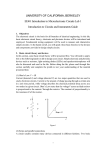
YOUR NAME: EE40/43/100 Spring 2012 YOUR PARTNER’S NAME: Lab 1: Resistive Circuits YOUR SID: V. Lee, T. Dear, T. Takahashi YOUR PARTNER’S SID: Pre-Lab: ___/10 Lab: ___/90 Total: ____/100 Resistive Circuits Lab 1: Resistive Circuits ELECTRICAL ENGINEERING 43/100 INTRODUCTION TO DIGITAL ELECTRONICS Department of Electrical Engineering and Computer Sciences Professor Ali Niknejad Lab Contents I. II. Lab Objectives Pre-‐Lab a. Pre-‐Lab Assignment b. Resistor Color Codes III. Lab Section a. A Word of Caution b. Lab Equipment i. The Digital Multimeter ii. The Programmable Power Supply iii. Solderless Protoboard (Breadboard) c. Resistive Networks d. Resistor Voltage Divider e. Introducing the myDAQ i. Basic Functions ii. Pin Outs iii. DMM IV. Lab Submissions a. Image Citations 1 Lab 1: Resistive Circuits EE43/100 Spring 2012 V. Lee, T. Dear, T. Takahashi Lab Objectives The lab is intended to introduce you to basic electrical components, and to help you become familiar with electronic equipment that you will use to design, build, and test circuits. In this lab, we will start by analyzing resistive circuits, and then later analyzing potentiometers. There is no post-‐lab section for this lab or any of the following labs; however, you are expected to complete all questions in these documents and turn it in as your lab report. You have two sections to complete this lab. These labs must be completed in pairs, but only one lab report per team is required. When you make measurements, where appropriate, please use at least 2 to 3 decimal places and include units. This is meant to be a two-‐week lab, so as to give you two sections to get used to the equipment and techniques used. In the first week, your GSI will mainly be discussing how to use each piece of equipment and showing demos. You are also encouraged to follow the videos on your own lab bench. Afterward, you will do the actual lab by following the instructions on this lab document and turning in the requested work. Pre-‐Lab Assignment 1. Make sure to have read the document for Lab 0 (just as an introduction). 2. Read the following section on Resistor Color Codes and complete the exercises. 3. Familiarize yourself with the rest of this document before arriving in lab! In addition, we recommend that you take a look at some documentation to learn the basics before you get started. Below are also links to some useful tutorials… Some guides on the various equipment: http://rfic.eecs.berkeley.edu/ee100/refs.html The EECS department has produced some nice videos walking you through the usage of the equipment: http://rfic.eecs.berkeley.edu/ee100/refs.html 2 Lab 1: Resistive Circuits EE40/43/100 Spring 2012 V. Lee, T. Dear, T. Takahashi Resistor Codes In every lab we will be using a lot of resistors, specifically many resistors of different values. So, how do we tell resistors apart? Every resistor has a series of color markings or bands that indicate the value of the resistor by the resistor color code. For most resistors, three closely-‐spaced color bands are followed by a fourth color band. The first two bands represent the first two significant figures of the resistor value, the third band corresponds to the multiplier as a power of ten, and the fourth band determines the resistor tolerance as a measure of possible resistor values within a certain range. Occasionally, there is a fifth band that indicates the quality in terms of the percentage of resistors that fail every 1000 hours. To calculate the value of the resistor, we interpret these color codes by using the following equation: c ab x 10 Ohms where a = the number corresponding to the first color band b = the number corresponding to the second color band c = the number corresponding to the third color bad Below is a table of corresponding numbers to each color in the resistor: Black Brown Red Orange Yellow Green Blue Violet Grey White 0 1 2 3 4 5 6 7 8 9 Ask your local circuits GSI if you need a mnemonic to remember this… For example, in Figure 1 we have the color band sequence blue-‐grey-‐brown-‐gold, which is read in that order. The blue band corresponds to 6 and the grey band corresponds to 8, which gives us 68. Combining this with the multiplier value of 1, we get 68×10! = 680Ω. The gold band corresponds to 5% tolerance, so the value of the resistor falls within the range 680 − .05 680 Ω and 680 + .05 680 Ω. i Figure 1 3 ii Figure 2 Lab 1: Resistive Circuits EE43/100 Spring 2012 V. Lee, T. Dear, T. Takahashi Now it’s your turn, given the color band sequence orange-‐orange-‐red-‐gold in Figure 2, what is the value of this resistor R? (Make sure to include units!) R = (2 pts) Given that the resistor tolerance band gold corresponds to 5% tolerance, what are the largest and smallest values this resistor can have (4 pts each)? (Ideally if the manufacturer did a good job, every resistor would be manufactured to have the same value.) Largest value = Smallest value = Public Service Announcement: PLEASE RETURN YOUR RESISTORS TO THE CORRECT BIN AFTER YOU FINISH THE LAB. IF YOU DON’T BAD THINGS MAY HAPPEN 4 Lab 1: Resistive Circuits EE40/43/100 Spring 2012 V. Lee, T. Dear, T. Takahashi Lab Section In our labs we will be working with electronic equipment to supply power. Before proceeding with the rest of this lab, please read the next section carefully… A Word of Caution In these labs you will be working with electronic equipment which supply power to your circuits. The labs in this course are designed to operate on voltages less than 25𝑉. These voltages level are not harmful and do not deliver sufficient energy to cause bodily harm (the resistance of your body is on the order of 300 to 1000Ω ). However, the equipment we are using is capable of generating higher voltages, which is powered by the high household power grid operating at 110 to 240𝑉. This can potentially be harmful. Another hazard in these labs is hot circuit components. At one point or another in these labs, you may connect something incorrectly and the component may get really hot. Be careful not to get burned! To avoid these hazards we highly recommend exercising the following precautions when working in the lab: 1. Turn off all power supplies when modifying a laboratory setup or performing manipulations that could potentially expose you to high iii voltage . 2. Set a current and voltage limit on any power supplies you use. We will discuss this later in the lab, but for now, be aware that current and voltage limits prevent electrical risks and protect your IC from going up in smoke. 3. Exercise extreme caution before touching a laboratory setup. Can you feel heat radiating from you circuit iv component? Consult your lab GSI if you’re not sure . 5 Lab 1: Resistive Circuits EE43/100 Spring 2012 V. Lee, T. Dear, T. Takahashi Lab Equipment: Digital Multimeter (DMM), Power Supply, and Solderless Protoboards All electronic gadgets need power to operate (or else they wouldn’t be “electronic”). Most systems require a specific supply voltage in order for the device to operate. For example, the “power brick” for a conventional laptop must supply 20V. You can usually find operating voltages on the labels of your electronic devices. Generally, power supplies and digital multimeters are the most common tools used for powering circuits and ensuring that circuits are functioning correctly. We will be using these tools for the majority of our labs. Download and read the instructions from the course web on how to operate the programmable laboratory supply and the digital multimeter. The link to the instructions can be found here. If you still do not understand how to operate the equipment, download the user’s manual or consult your lab GSI. The Digital Multimeter (DMM) v Agilent DMM 34401A The digital multimeter measures a number of different quantities, from capacitance and resistance, to frequency. In this lab, we are most interested in voltage and current. We will use the DMM not only to check the output of the circuits we design, but also to verify our setup. Some of the questions you should consider when using the DMM are: Does the voltage supplied to the circuit have the correct value? Is the supply current in the expected range (i.e. not something like 10kAmps)? Performing sanity checks like these will make your life much easier in the lab. The Programmable Power Supply In many applications, electronic equipment is powered by batteries. However, prototyping circuits that are battery powered is problematic because discharged batteries are always a hazard. The power supply eliminates this problem. 6 Lab 1: Resistive Circuits EE40/43/100 Spring 2012 V. Lee, T. Dear, T. Takahashi vi Agilent E3631 Programmable Power Supply The programmable power supply also helps us avoid inconsistencies in powering our circuits by delivering a constant voltage, which you can set by changing the output voltage. Most laboratory supplies also have a current limit feature that you can use to set the maximum current the supply will deliver regardless of what voltage you specify. Why should we set the current limit? vii Your new IC chip Suppose you are testing a new circuit with your brand new $1 million chip. You expect your new chip to nominally draw 100𝑚𝐴. But unfortunately for you, you wired something wrong and instead of drawing 100𝑚𝐴 your chip draws 1𝑘𝐴 (10! times what you expected it to draw!). Your basic physics class in high school taught you that power is proportional to voltage times current (𝑃 = 𝐼𝑉). Even if voltage is set at 1V, your brand new $1 million chip has dissipated a lot of power in the form of wasted heat. Now, your brand new $1 million chip is fried or your programmable power supply needs a new fuse. The current limit is designed to prevent exactly this. The current limit will prevent the output current from exceeding a certain value so that excessive current flow will not destroy your setup. We usually set the current limit at a small margin above nominal draw. (Usually 100mA to 200mA is usually a good start). 7 Lab 1: Resistive Circuits EE43/100 Spring 2012 V. Lee, T. Dear, T. Takahashi Now for a few quick questions… Suppose you have designed a new audio amplifier and are now ready to test it in the laboratory. According to the design, the circuit can be modeled as a 1𝑘Ω resistor and we need to apply a voltage 𝑉!! across it. To ensure that your circuit does not go up in smoke like the $1 million chip in the previous example, we set the current limit to 𝐼!"# . For the following values of 𝑉!! and 𝐼!"# what voltage and current will your power supply actually provide in this setup? (Hint: given the resistance, determine if the circuit draws more current that the current limit) Let 𝑉!! = 5𝑉 and 𝐼!"# = 10𝑚𝐴 as your values. _________________ (2 pts each) What if 𝑉!! = 10𝑉 and 𝐼!"# = 5𝑚𝐴 are your values? (2 pts each) Solderless Protoboards (Breadboards) In the following exercises, you will be using the solderless protoboard, known affectionately as the breadboard. The breadboard is a convenient set of traces that help you prototype your circuit by providing sets of pre-‐made connections. A series of wire or metal contacts within the breadboard allow current and voltage to flow through the prototyped circuit. The figure below indicates which holes on the breadboard are connected. viii A typical breadboard and its traces Notice that the breadboard at your station looks slightly different but the connections follow the same pattern. Also note that there are designated banana plug connectors on the breadboard. Be aware that these connectors do not connect to any other part of the board by themselves. In order to use the banana plug connectors, you have to wire them to appropriate traces on the board. Also notice the red and blue traces are longer than the traces in the middle of the board. These red and blue traces are usually designated as power traces. There you should hook up your positive and negative supplies. It is strongly recommended that you connect your supplies to your power traces as opposed to some random trace on the breadboard, so that it allows convenient access and organization to the supplies and ground connections. 8 Lab 1: Resistive Circuits EE40/43/100 Spring 2012 V. Lee, T. Dear, T. Takahashi Resistive Networks Now let’s move on to a resistive network problem. Your first task will be to calculate the voltage value at Node2 in the figure below. And the next thing will be to build the circuit on the protoboard. Using the DMM, measure the value of the voltage at Node 2 of the circuit and compare it to the value you get in the calculation. If you don’t know how to connect the DMM correctly, ask your GSI for help. By now you should have gotten some values from your hand calculation as to what the voltage is at each node of the circuit. In the space provided below, record your voltage measurements for Node 2. It should not match the simulator value exactly. Explain why this is the case. Score: __/7 9 Lab 1: Resistive Circuits EE43/100 Spring 2012 V. Lee, T. Dear, T. Takahashi Now let’s examine the behavior of resistors. You already have learned that when we put resistors in series the equivalent resistance 𝑅!" of a series of n resistors is equal to: ! 𝑅!" = R ! 𝐸𝑞𝑢𝑖𝑣𝑎𝑙𝑒𝑛𝑡 𝑅𝑒𝑠𝑖𝑠𝑡𝑎𝑛𝑐𝑒 𝑖𝑛 𝑆𝑒𝑟𝑖𝑒𝑠 !!! 1 Figure 2-‐17: In a single-‐loop circuit, 𝑅!" is equal to the sum of the resistors. And for a network of 𝒏 parallel resistors, the equivalent resistance 𝑅!" is equal to: ! 𝑅!" = !!! 1 𝑅! !! 𝐸𝑞𝑢𝑖𝑣𝑎𝑙𝑒𝑛𝑡 𝑅𝑒𝑠𝑖𝑠𝑡𝑎𝑛𝑐𝑒 𝑖𝑛 𝑃𝑎𝑟𝑎𝑙𝑙𝑒𝑙 In a relatively simple resistive network, we can use these rules to implement another rule: the voltage divider. The voltage divider equation allows you to calculate the voltage across certain resistor configurations Figure 2-‐21: Voltage source connected to a parallel combination of 2 three resistors. 1 Ulaby and Maharbiz. Circuits, Figure 2-17 10 Lab 1: Resistive Circuits EE40/43/100 Spring 2012 V. Lee, T. Dear, T. Takahashi Resistor Voltage Divider Sometimes you just can’t get you what you need to power your device properly. You have a 9V battery but your circuit runs on 2 AA batteries (3V). So what do you do? A rather primitive solution is to use a voltage divider to step down a higher voltage to a lower one. Suppose we have a voltage source VS and we want to use that to deliver a certain voltage VL to a device (assume 𝑉! < 𝑉! ). In addition, we want to accomplish this using only resistors and the voltage source using voltage division. Let’s do some calculations to figure out what resistor values to use. The circuit in consideration looks like the following: The resistance XL of a practical load (the device) will vary, so we will not be able to get the exact desired load voltage at all times. Instead, we will compromise with an acceptable range for VL. Suppose that VL must range between VL,min and VL,max. Then the allowable change in VL is ΔVL = VL,max -‐ VL,min. In addition, we want to minimize unnecessary power dissipation by limiting the amount of current in the circuit to avoid burning out components. Therefore, we need to make sure iL will not exceed some current limit iL,max. Considering these constraints, we want to solve for optimal R1 and R2 in terms of VS, VL,max, ΔVL, and iL,max. It is easier to calculate by first expressing the above circuit as this equivalent circuit: 2 Ulaby and Maharbiz. Circuits, Figure 2-21 11 Lab 1: Resistive Circuits EE43/100 Spring 2012 Show that the follow relationships hold: 𝑉!! = 𝑉! 𝑅 ! = V. Lee, T. Dear, T. Takahashi 𝑅! 𝑅! + 𝑅! 𝑅! 𝑅! 𝑅! + 𝑅! Score: _ / 10 By looking at the equivalent circuit we see that we need to achieve a balance: we want R’ to be small enough so that ΔVL is small, but we also want R’ to be large enough so the current stays under iL,max. 1. The highest output voltage VL,max occurs when XL ∞, in other words, when the load acts like a open circuit. What is VL,max in terms of VS’ and R’? _______________________________________ (2 pts) 2. VL,min occurs when iL = iL,max. Express VL,min in terms of VS’, R’, and iL,max. _______________________________________ (2 pts) 3. Find ΔVL from parts 1 and 2. _______________________________________ (2 pts) 12 Lab 1: Resistive Circuits EE40/43/100 Spring 2012 V. Lee, T. Dear, T. Takahashi Solve the equations from parts 1 and 3 simultaneously to find R1 and R2 in terms of VS, VL,max, ΔVL, and iL,max. Score: _ / 15 R1 = R2 = Now that you’ve derived the formulas for the resistances satisfying the parameters, let’s actually build the circuit. Supposed we want to use our circuit to step down a supply voltage of 𝑉! = 9𝑉 to power a load with that requires a supply voltage 𝑉! = 3𝑉 ± 25% to operate. We also want the maximum current running through the load to be 𝑖!"# = 10𝑚𝐴. 13 Lab 1: Resistive Circuits EE43/100 Spring 2012 V. Lee, T. Dear, T. Takahashi What are values of 𝑅! and 𝑅! should you use? (2 pts each) 𝑅! = 𝑅! = For our prototype we will be using a variable resistor or a potentiometer to change the load to the circuit. The symbol for a potentiometer is shown in the figure to the 3 left. To simulate the variable load, we will be connecting the A and W terminals of the potentiometer as our 𝑋! load. Once you have built your circuit, adjust the potentiometer and verify that the output voltage across the load stays within the range specified by the parameters. For loads close to zero, obviously we will not be able to satisfy the parameters so don’t worry about those loads when you adjust the potentiometer. The potentiometer has three pins. The two outer pins will always have the same resistance across them. The resistance between the middle and each of the outer pins will vary as you turn the knob. Finally, the resistance between the first outer pin and the middle pin, plus the resistance of the second outer pin and the middle pin, should add up to the resistance between the two outer pins at all times. Show this setup to your GSI for check off, but don’t take it apart just yet… Your GSI Signs Here (20 pts) Introducing the myDAQ Device In this last section, we will be introducing a new tool called the myDAQ that you may find useful at home for your labs. This section is a bit of literature but it’s better than reading a manual. If you prefer reading the manual, it can be found here . Notice how all the equipment on your lab bench is pretty heavy-‐duty? That’s inconvenient, since you’re pretty much forced to come to the lab to do your work. Not so if you have the myDAQ. This portable little device combines all the functionality of each piece of equipment into one little box. All you need are some cables, some wires, and your computer, and you are good to go. Take a look at the diagram of the myDAQ device below… 3Ulaby and Maharbiz. Circuits, Figure 2-3 (b) 14 Lab 1: Resistive Circuits ix EE40/43/100 Spring 2012 V. Lee, T. Dear, T. Takahashi Using Basic Functions of myDAQ On your computer under Programs, you should find the software for the myDAQ under National Instruments -‐> NI ELVISmx for NI ELVIS & NI myDAQ. Under NI ELVISmx for NI ELVIS & NI myDAQ, you will find the NI ELVISmx Instrument Launcher. Opening this program should launch the toolbar shown below: Each icon on this toolbar is a virtual instrument that you can run on your computer. The virtual instrument will use input from the myDAQ to perform measurements. Our myDAQ comes with the following virtual instruments: -‐ -‐ -‐ -‐ -‐ DMM – Digital Mulitimeter Scope – Your good old oscilloscope Bode – Bode plotter DSA – Dynamic Signal Analyzer ARB -‐ Arbitrary Waveform Generator 15 Lab 1: Resistive Circuits -‐ -‐ EE43/100 Spring 2012 V. Lee, T. Dear, T. Takahashi DigIn – Digital Reader DigOut – Digital Writer We won’t be using most of these instruments. We are only interested in the DMM, Scope, and FGEN instruments since those are the ones you are familiar with. In addition, don’t worry about the instruments that you cannot access. These instruments are intended for use on another device. You might be wondering where the power supplies are. The myDAQ does not come with a programmable power supply but comes with several constant supplies which will be discussed in the next section. Pin Outs on the myDAQ You will notice that on the side of the myDAQ there are a set of 20 pins with various labels on them. Some of these pins are power sources and others are digital/analog I/Os. For most of the labs, we will not be using the I/O pins too much since this is primary a circuits course, not a programming course. The first set of pins we want you to take note off are the left most 3 pins labeled +𝟏𝟓𝑽, −𝟏𝟓𝑽, and 𝑨𝑮𝑵𝑫. These correspond to your positive and negative voltage supplies with common ground. The second set of pins we want you to note are on the right side of the myDAQ. These pins are labeled 𝐷𝐺𝑁𝐷 and 5𝑉. These two pins correspond with your positive 5 volt supply and ground. In addition to these power supplies, you will notice that there are a set of analog output pins AO, analog input pins AI(±10𝑉), and digital input/output pins DIO on the myDAQ. Each set of pins is grouped together with an arrow. The pins that fall under the arrow are all linked to the ground pin that the arrow point to. We will be using these pin outs as our sources when you are building circuits outside of the lab. The Digital Mulitimeter (DMM) Now let’s take a look at the DMM. On the ELVISmx Instrument Launcher, launch the DMM program. The following window should appear: 16 Lab 1: Resistive Circuits EE40/43/100 Spring 2012 V. Lee, T. Dear, T. Takahashi You will notice that there is a diagram showing the Banana Jack Connections. Make sure to plug in the probes that came with the myDAQ to the correct inputs. To run the instrument, hit the “Run” button. This will initialize the virtual instrument and you are now set to make measurements. By default, the instrument will initialize to measure voltage. Try measuring a battery or something with a voltage 4 potential to test if your myDAQ is working. If you want to change the quantity that is being measured, simply toggle the Measurement Setting to the desired 5 quantity. Using the same resistive divider and potentiometer circuit from the last part, replace the power supply with the myDAQ’s 15-‐V supply. Use the built-‐in DMM to measure the voltage across the potentiometer and show the setup to your GSI for check off. Your GSI Signs Here (20 pts) Once you finish, feel free to play around with the other equipment and the myDAQ. You will be learning about them soon enough! 4 NEVER PROBE THE OUTPUT OF A WALL SOCKET. THIS IS POTENTIALLY VERY HARMFUL SINCE THE LINE OPERATES AT 120 VAC. 5 Note that for measurements such as current, you will have to change the connector the high (red) probe is connected to. 17 Lab 1: Resistive Circuits EE43/100 Spring 2012 V. Lee, T. Dear, T. Takahashi Lab Report Submissions This lab is at the beginning of the lab section. Make sure you have completed all questions and drawn all the diagrams for this lab. In addition, attach any loose papers specified by the lab and submit them with this document. These labs are designed to be completed in groups of two. Only one person in your team is required to submit the lab report. Make sure the names and student IDs of BOTH team members are on this document (preferably on the front). Image Citations Textbook Images are courtesy of Fawwaz T. Ulaby and Michel M. Maharbiz and National Technology and Science Press. Fawwaz T. Ulaby and Michel M. Maharbiz, Circuits © 2009 National Technology and Science Press Additional Citations www.parts.digikey.es www.ca.digikey.com iii www.constructionstore.co.uk iv www.speedysigns.com v home.agilent.com vi www.triosmartcal.com.au vii www.octopart.com viii www.engr.astate.edu ix http://www.ni.com/mydaq/specifications.htm i ii 18