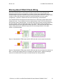
1
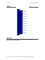
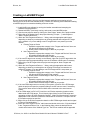
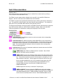
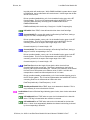
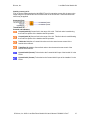
Low-Side Driver Module Kit User’s Manual D000030 Rev F January 2009 Drivven ,Inc. • 12001 Network Blvd, Bldg E, Suite 110 • San Antonio, Texas 78249 • USA Phone : 210.248.9308 Web : www.drivven.com , E-mail : [email protected] Drivven, Inc. Low-Side Driver Module Kit Contents Introduction ...................................................................................................................................... 3 Pinout............................................................................................................................................... 4 Hardware ......................................................................................................................................... 4 Powering the Module ....................................................................................................................... 5 Platform Compatibility ...................................................................................................................... 6 Low-Side Drivers ............................................................................................................................. 7 Software Installer ............................................................................................................................. 9 Creating a LabVIEW Project.......................................................................................................... 10 Sub VI Documentation ................................................................................................................... 12 Warning About FPGA I/O Node Wiring ......................................................................................... 16 © Drivven, Inc. 2009 • Low-Side Driver Module Kit User’s Manual • D000030 • Rev F 2 Drivven, Inc. Low-Side Driver Module Kit Introduction The Low-Side Driver Module Kit provides a CompactRIO (cRIO) module for driving general purpose automotive solenoid valves. The kit includes a LabVIEW FPGA VI for controlling all driver channels independently. Each general purpose low-side solenoid driver is PWM controlled, capable of 0-100% duty cycle operation. Channels 5-8 are capable of driving low impedance solenoids with a programmable peak-hold current profile. The high and low current limits may be set independently for each channel. Features: ¾ 8-channel general purpose low-side solenoid driver o 1.2A continuous duty (channels 1-4) o 2A continuous duty (channels 5-8) o Individual dual current limit profiles for channels 5-8 50mA to 4A high current limit range (during peak time) 50mA to 2A low current limit range 2 mA current limit resolution o PWM controlled with 0-100% duty cycle operation o Open/short circuit detection and reporting with short circuit disable ¾ External power supply of 6-32V Note: Channels 5 & 6 have a combined current rating of 3A continuous. Note: Channels 7 & 8 have a combined current rating of 3A continuous. © Drivven, Inc. 2009 • Low-Side Driver Module Kit User’s Manual • D000030 • Rev F 3 Drivven, Inc. Low-Side Driver Module Kit Pinout Hardware The Low-Side Driver Module Kit provides eight general purpose low-side solenoid drivers in a National Instruments CompactRIO module. © Drivven, Inc. 2009 • Low-Side Driver Module Kit User’s Manual • D000030 • Rev F 4 Drivven, Inc. Low-Side Driver Module Kit Powering the Module The Low-Side Driver module requires power from two different sources. One source is from the CompactRIO backplane male high density D-Sub 15-pin (HD15) connector which mates with the module’s female HD15 connector. This power source provides a regulated 5 volts and ground to various digital logic functions within the module. The CompactRIO 5V source is active whenever the CompactRIO or R-Series Expansion Chassis is properly powered. The module should only be powered at the HD15 connector by plugging it into a CompactRIO or R-Series Expansion Chassis. The module’s HD15 connector should not be connected to any other device. Another required power connection is at the external screw terminal connector. The terminals are labeled BATT (0) and GND (9). Typical power sources will be from automotive 12V or 24V battery systems. However, the module can accept power from a range of 6V to 32V. With all channels disabled, the module requires up to 100mA from the external supply. However, the external supply must be capable of powering the actuators connected to the module. Therefore a battery or power supply capable of 10A may be necessary under full load. The external battery power ground is completely isolated, within the module, from the CompactRIO 5V supply ground. However, the external battery ground and the CompactRIO ground may be connected externally. In order for the module to be recognized by the Drivven FPGA sub VI, it must be powered by the external supply. Warning: The external battery supply input terminals are not reverse voltage polarity protected. Connecting power to the module in reverse polarity will damage the module. This event is not covered by the warranty. Please refer to the DrivvenReverseBatteryNotice.pdf document (available on the website) for a recommended solution for protecting a system from reverse battery polarity. © Drivven, Inc. 2009 • Low-Side Driver Module Kit User’s Manual • D000030 • Rev F 5 Drivven, Inc. Low-Side Driver Module Kit Platform Compatibility CompactRIO modules from Drivven are compatible within two different platforms from National Instruments. One platform is CompactRIO, consisting of a CompactRIO controller and CompactRIO chassis as shown in Figure 1a below. Figure 1a. CompactRIO platform compatible with Drivven CompactRIO modules. The other platform is National Instruments PXI which consists of any National Instruments PXI chassis along with a PXI RT controller and PXI-78xxR R-Series FPGA card. An R-Series expansion chassis must be connected to the PXI FPGA card via a SHC68-68-RDIO cable. The CompactRIO modules insert into the R-Series expansion chassis. This platform is shown in Figure 1b below. Figure 1b. PXI platform compatible with Drivven CompactRIO modules. Drivven CompactRIO modules are not compatible with the National Instruments CompactDAQ chassis. Drivven CompactRIO modules REQUIRE one of the hardware support systems described above in order to function. The modules may not be used by themselves and/or interfaced to third party devices at the backplane HD15 connector. These efforts cannot be supported by Drivven or National Instruments. © Drivven, Inc. 2009 • Low-Side Driver Module Kit User’s Manual • D000030 • Rev F 6 Drivven, Inc. Low-Side Driver Module Kit Low-Side Drivers The low-side drivers are capable of driving a wide variety of automotive relays and actuators. Examples of actuators include EGR valves, turbo wastegate valves, fuel pressure regulators, and transmission solenoid actuators. Channels 1-4 are low-side switches for inductive loads which can drive up to 1.2 amps. Channels 5-8 are programmable current-limited drivers which can drive up to 4 amps during PeakTime and 2 amps in continuous hold mode. These channels are useful for low-impedance solenoids. Channels 5-8 operate identically to PFI channels 1-4 of the PFI driver module. One useful application of these channels would be for typical low impedance fuel injector valves which need to be operated according to duty cycle as opposed to crankshaft position. They may also be used for common rail fuel pressure regulator valves which often require current drives from 0 to 2A. WARNING: Do not attempt to drive low impedance injectors or solenoids with the general purpose low-side driver channels 1-4. Channels 1-4 are only rated for 1.2 amps continuous. When using channels 1-4, if a solenoid requires greater than 1.2A current drive, channels 1-4 can be connected to a single solenoid in parallel. In order to control the parallel channels in sync, connect the lowside FPGA VI channel controls to the same control parameters within the FPGA. For example, to drive a solenoid with up to 3.6A, PWMEnable1, PWMEnable2 and PWMEnable3 can be controlled by a single enable Boolean at the FPGA level. A similar parallel connection should also be made for PWMPeriod and PWMPulseWidth. This method should not be applied to channels 5-8. Each channel is independently controlled within the module via pulse-width modulation (PWM). PWM duty cycle from 0 to 100% is possible. Software on the RIO FPGA device communicates several parameters for each channel to operate. Those parameters are Enable, Period and PulseWidth. All parameters are communicated serially at 200 usec intervals. Each PWM controller utilizes a 20-bit timer operating at 2 MHz. This provides a resolution of 500 nsec and a minimum PWM frequency of 1.9 Hz. Since 0% and 100% duty cycles are possible, relays and actuators may be controlled in continuous on or off states. Each low-side driver channel automatically tests for open circuit conditions. When the low-side switch is commanded open, the circuit is tested for an open condition. Upon detection of an open circuit, an open circuit error flag will be reported. The open circuit flag is automatically cleared when the condition is removed. Each low-side driver channel automatically protects itself from an accidental short circuit to battery. When the low-side switch is commanded closed, the circuit is tested for a short. Upon detection of a short, a short circuit error flag will be reported for the channel and the channel will be disabled until software clears the error flag. The short circuit error flag for each channel will not be cleared while the switch is being commanded closed. It is strongly recommended that the user not continually clear the short circuit error flags, as this may lead to driver circuit damage in the event of an actual short circuit. Even though the short circuit detection and disable feature is present, it is strongly recommended that the wiring harness include a 7 amp fuse for four solenoids as shown in Figure 2. © Drivven, Inc. 2009 • Low-Side Driver Module Kit User’s Manual • D000030 • Rev F 7 Drivven, Inc. Low-Side Driver Module Kit Battery or Power Supply (12V Typical @ >5A) + 0 1 2 3 4 5 6 7 8 9 Lowside Module Connector Automotive 5A Fuse Relay or Actuator Relay or Actuator Relay or Actuator Relay or Actuator Figure 2. Connecting general purpose solenoids to the low-side driver channels Current Limit Features of Channels 5-8 Channels 5-8 have the ability to limit the current according to programmable current setpoints. Each channel has a high and low current limit. The high current limit is effective when the drive pulse starts and extends for the time period specified by PeakTime for each channel. After the peak time expires, the low current limit setting takes effect until the pulse ends. The high current limit setting has a useful range of 50mA to 4A and will be in effect for the time specified by the PeakTime parameter. The low current limit setting has a useful range of 50mA to 2A and will be in effect for the remainder of the PWM command pulse. The current ranges must not be exceeded or damage could occur to the channel. When driving solenoids which do not required peak/hold current profiles, it is recommended to set the high current limit value equal to the low current limit value and set PeakTime to a minimum of 50 usec. Warning: Channels 5 and 6 have a combined total continuous current limit of 3A. Channels 7 and 8 have a combined total continuous current limit of 3A. During normal operation, channels 5-8 will disable the channel when a short circuit is detected and will also set a short circuit flag in software. However, when current limit settings are below 700mA, the channels will falsely report a short circuit and disable the channel until the short circuit flag is cleared. When current limits are desired below 700mA then the ShortReportDisableX Boolean must be set to TRUE so that short circuits will not be reported and the channel will not be disabled. However, the channel is still protected from short circuits because the current limit control feature is fast enough to prevent excessive currents. © Drivven, Inc. 2009 • Low-Side Driver Module Kit User’s Manual • D000030 • Rev F 8 Drivven, Inc. Low-Side Driver Module Kit Software Installer The Low-Side Driver Module Kit is provided with an installer package which may be downloaded from Drivven’s Sharepoint website after obtaining login access from Drivven. User’s may go to http://portal.drivven.com/SoftwareDownload and enter the provided username and password to gain access to the specific product installer packages which have been purchased. The installer packages are executables which should be run on the intended development computer, having LabVIEW development tools installed. After installing the package, a “Start->Programs->Drivven>ProductRelease” menu item will be added to the desktop. The specific product will have an example LabVIEW project appear under the “Examples” menu and the user manual will appear under the “Manuals” menu. User’s may copy and open the example project to experiment with the module or use as a starting point for a new application. All software files, example projects and documentation are installed to: C:\Program Files\National Instruments\LabVIEW X.X\vi.lib\addons\DrivvenProductRelease\. When working with block diagrams, user’s will notice a “Drivven” function palette added to the standard LabVIEW palette, specific for the RT or FPGA target. VIs for a specific Drivven product will be categorized according to product name. Also, some Drivven products will install RT and FPGA VIs under a “General” function palette which is intended to be used across multiple products. Requirements The Drivven VIs require: ¾ LabVIEW 8.5 Full Development or later ¾ LabVIEW RT Module 8.5 or later ¾ LabVIEW FPGA Module 8.5 or later ¾ NI-RIO 2.4 or later The Low-Side Driver Module Kit is provided with a LabVIEW FPGA VI for commanding each lowside switch individually via PWM. Figure 3. lowside_revx.vi icon with leads. The FPGA VI must be placed within a Single Cycle Loop (SCL) of a LabVIEW FPGA block diagram. The SCL must execute at the default clock rate of 40 MHz. The FPGA VI requires a pre-synthesized netlist file having a matching name and an extension of .ngc. The netlist file must be located in the same directory as the matching VI. The installer will place this file in the LabVIEW addons directory along with the FPGA VI. © Drivven, Inc. 2009 • Low-Side Driver Module Kit User’s Manual • D000030 • Rev F 9 Drivven, Inc. Low-Side Driver Module Kit Creating a LabVIEW Project Drivven recommends working from the provided example application as a starting point for learning the use of the Drivven software blocks. However, the following section describes starting a LabVIEW project from scratch and adding a Drivven module. 1.) Install the Drivven software by running the installer executable and accepting the software license agreement. 2.) Restart LabVIEW, if previously running, and create a new LabVIEW project. 3.) Give the new project a name by clicking the “Save Project” button on the project toolbar. 4.) Right click on the highest item in the project hierarchy (“Project:…”) and navigate to “New->Targets and Devices…” 5.) Within the “Add Targets and Devices…” dialog, select the appropriate radio button, depending on whether you already have an existing powered and configured RT target on the network or if you are adding a new RT target which is not present yet on the network. a. Existing Target or Device i. Expand the appropriate category in the “Targets and Devices” list to see the discovered targets in that category. ii. Double-click the desired target to add it to your project. b. New Target or Device i. Expand the appropriate category in the “Targets and Devices” list to see all possible targets within that category. ii. Double-click the desired target to add it to your project. 6.) If the new RT target is not currently on the network, right-click on the RT target within the project and open the properties dialog to set the IP address or DNS name if necessary. 7.) Right-click on the RT target within the project and navigate to “New->Targets and Devices…” 8.) Within the “Add Targets and Devices…” dialog, select the appropriate radio button, depending on whether you already have an existing FPGA target connected to an existing RT target or if you are adding a new FPGA target which is not present yet. a. Existing Target or Device i. Expand the appropriate category in the “Targets and Devices” list to see the discovered FPGA targets in that category. ii. Double-click the desired target to add it to your project. b. New Target or Device i. Expand the appropriate category in the “Targets and Devices” list to see all possible targets within that category ii. Double-click the desired target to add it to your project. 9.) If the new FPGA target was not currently in the system, right-click on the FPGA target within the project and open the properties dialog to set the resource name if necessary. The resource name can be found from MAX when connected to the actual remote system. 10.) If the FPGA target is a PXI or PCI card, then an R Series expansion chassis must be added under the FPGA target. This is done by right-clicking on the FPGA target and navigating to “New->R Series Expansion Chassis”. Within the following dialog, select the appropriate FPGA connector to which the chassis will be connected. A unique name for the chassis may also be specified. 11.) Right click on the R-Series expansion chassis or cRIO FPGA target chassis and navigate to “New->C Series Modules…” 12.) Select the “New Target or Device” radio button and double-click on the “C Series Module” in the “Targets and Devices” list. In the following dialog, select the desired Drivven module at the bottom of the “Module Type” list. The Drivven modules will be appended © Drivven, Inc. 2009 • Low-Side Driver Module Kit User’s Manual • D000030 • Rev F 10 Drivven, Inc. Low-Side Driver Module Kit there if any Drivven module software has been installed. Select the appropriate module location. Finally, specify an appropriate name for the module, which will later appear in the FPGA I/O nodes in the FPGA block diagram. Having meaningful module names is important for preventing coding mistakes. 13.) After adding a module to the project, a folder will automatically be added to the project having the same module name given in the module configuration dialog. The folder will contain the FPGA I/O pins for the module slot. These I/O pins can be selected in the block diagram when connecting the module VI PinInput and PinOutput clusters to FPGA I/O nodes. The example application, discussed below, should be consulted for further details about connecting the PinInput and PinOutput clusters to FPGA I/O nodes. Within the example projects, notice the FPGA I/O node elements having module name prefixes. 14.) Some Drivven modules can be automatically recognized by LabVIEW when adding cRIO modules to the project. However, Drivven does not recommend using this feature because the module names, which are automatically assigned, are not meaningful (Mod1, Mod2, etc) and can lead to coding mistakes when wiring the Drivven FPGA VIs to the I/O nodes. Adding the modules to the project manually, as described above, is still the recommended method. © Drivven, Inc. 2009 • Low-Side Driver Module Kit User’s Manual • D000030 • Rev F 11 Drivven, Inc. Low-Side Driver Module Kit Sub VI Documentation lowside_revf.vi This VI is for interfacing directly with the Drivven LowSide Driver module and for providing a control interface to the LabVIEW RT level. The FPGA VI must be placed within a Single Cycle Loop (SCL) of a LabVIEW FPGA block diagram. The SCL must execute at the default clock rate of 40 MHz. The FPGA VI requires a pre-synthesized netlist file having a matching name and an extension of .ngc. The netlist file must be located in the same directory as the matching VI. The installer will place this file in the LabVIEW addons directory along with the FPGA VI. The PinInput and PinOutput clusters are wired to LabVIEW FPGA I/O nodes which are configured for a cRIO controller chassis or a cRIO R-Series expansion chassis. Refer to the LabVIEW FPGA documentation for details about creating and configuring FPGA I/O nodes. Connector Pane Controls and Indicators LowSidePinInput These Boolean controls must be connected to their corresponding FPGA I/O Node input item. LowSidePinOutput The Boolean indicator named IDSelectEn must be connected to a Set Output Enable method of an FPGA I/O Method Node. The Boolean indicator named IDSelectOut must be connected to a Set Output Data method of an FPGA I/O Method Node. The remaining Boolean indicators must be connected to their corresponding FPGA I/O Node output item. LowSideControl This cluster of parameters enable each channel and control the PWM action to the lowside switches. PWMEnableX When TRUE, the PWM controller is enabled. When FALSE (default), the PWM controller is disabled. PWMPeriodX The time period between leading edges of low-side switch closure. PWMPeriod is entered in terms of 2 MHz clock ticks and is internally limited to 20 bits. This provide a maximum period of 0.524 seconds or a frequency of 1.9 Hz, and a resolution of 500 nsec. Values larger than 20 bits will roll over from zero. Drivven provides lowside2ticks_revf.vi in the lowside function group in the RT function palette. This VI can be implemented at the LabVIEW RT level for converting PWM frequency and duty cycle to PWMPeriod ticks and PWMPulseWidth ticks. PWMPeriod(uint32 clock ticks) = 2,000,000 / Frequency(Hz) PWMPulseWidthX The time during each PWMPeriod in which the low-side switch is closed. The low-side switch is closed from the beginning of PWMPeriod until PWMPulseWidth expires. PWMPulseWidth is entered in terms of 2 MHz clock ticks and is internally limited to 20 bits. While PWMPulseWidth is 0 the © Drivven, Inc. 2009 • Low-Side Driver Module Kit User’s Manual • D000030 • Rev F 12 Drivven, Inc. Low-Side Driver Module Kit low-side switch will remain open. While PWMPulseWidth is greater than or equal to PWMPeriod, the low-side switch will remain closed. Values larger than 20 bits will roll over from zero. Drivven provides lowside2ticks_revf.vi in the lowside function group in the RT function palette. This VI can be implemented at the LabVIEW RT level for converting PWM frequency and duty cycle to PWMPeriod ticks and PWMPulseWidth ticks. PWMPulseWidth(uint32 clock ticks) = DutyCycle * 20,000 / Frequency(Hz) LSFaultClr When TRUE, clears all low-side driver short circuit fault flags. CurrentLimitXH The current limit setting in effect during PeakTimeX, having a range of 0 to 1900, corresponding to 0 to 4A. Drivven provides lowside_current_ctrl.vi in the lowside function group in the RT function palette. This VI can be implemented at the LabVIEW RT level for converting current limit in amps to the integer range of 0 to 1900. CurrentLimit(uint16) = CurrentLimit(A) * 475 CurrentLimitXL The current limit setting in effect during PeakTimeX, having a range of 0 to 950, corresponding to 0 to 2A. Drivven provides lowside_current_ctrl.vi in the lowside function group in the RT function palette. This VI can be implemented at the LabVIEW RT level for converting current limit in amps to the integer range of 0 to 1900. CurrentLimit(uint16) = CurrentLimit(A) * 475 PeakTime Determines the length of time that the driver circuit will use CurrentLimitXH as the current limit. PeakTime is entered as a uint8 value in terms of 2 MHz clock ticks divided by 64. Therefore, the maximum value entered for PeakTime of 255 equates to an effective value of 16320. At 2 MHz this corresponds to a maximum delivered peak time of 8.16 msec. Drivven provides lowside_peaktime2ticks_revf.vi in the lowside function group in the RT function palette. This VI can be implemented at the LabVIEW RT level for converting PeakTime in milliseconds to 2 MHz clock ticks. PeakTime(uint8 ticks) = PeakTime(msec) * 31.25 ShortReportDisableX When TRUE, short circuit detection is disabled. This is only necessary for current limits below 700mA. LowSideData Cluster of Boolean flags indicating open circuits, short circuits and module present. LSFaultOpenX Set to TRUE when an open circuit is detected for the low-side driver. The flag is cleared when the condition is removed. LSFaultShortX Set to TRUE when a short circuit is detected for the low-side driver. A short circuit automatically disables the channel until the flag is cleared by the corresponding LSFaultClr. © Drivven, Inc. 2009 • Low-Side Driver Module Kit User’s Manual • D000030 • Rev F 13 Drivven, Inc. Low-Side Driver Module Kit ModulePresent Indicates that the module is externally powered, inserted in the configured cRIO slot and recognized by the lowside FPGA VI. lowside2ticks_revf.vi Converts frequency and duty cycle to 2MHz clock ticks to be wired to the PWMPeriod and PWMPulseWidth inputs of the lowside FPGA VI. Connector Pane Controls and Indicators Frequency (Hz) PWM Frequency specified to the lowside channel. DutyCycle (%) PWM Duty Cycle specified to the lowside channel. LSPeriodTicks PWM period in 2MHz clock ticks. LSPulseWidthTicks PWM pulse width in 2MHz clock ticks. lowside_peaktime2ticks_revf.vi Converts time in milliseconds to clock ticks. The output of this VI should be wired to the PeakTime input of the lowside VI in the FPGA. PeakTime(uint8 ticks) = PeakTime(msec) * 31.25 Connector Pane Controls and Indicators PeakTime (msec) Peak time for the lowside channel in milliseconds. Ticks Peak time for the lowside channel in clock ticks. © Drivven, Inc. 2009 • Low-Side Driver Module Kit User’s Manual • D000030 • Rev F 14 Drivven, Inc. Low-Side Driver Module Kit lowside_current_ctrl.vi \This VI can be implemented at the LabVIEW RT level for converting current limit in amps to the integer range for CurrentLimitXH and CurrentLimitXL at the FPGA level. Scalar and offset trim values may be applied. Connector Pane Controls and Indicators CurrentLimitH (A) Current limit in the range of 0 to 4A. This limit value is used during the PeakTime portion of the lowside channel operation. CurrentLimitL (A) Current limit in the range of 0 to 2A. This limit value is used following the PeakTime portion of the lowside channel operation. TrimScalar Multiplier to CurrentLimit value to trim the actual current control of the lowside driver channel. TrimOffset (A) Added to CurrentLimit value to trim the actual current control of the lowside driver channel. CurrentLimitH (Counts) To be wired to the CurrentLimitXH input of the lowside VI in the FPGA. CurrentLimitL (Counts) To be wired to the CurrentLimitXL input of the lowside VI in the FPGA. © Drivven, Inc. 2009 • Low-Side Driver Module Kit User’s Manual • D000030 • Rev F 15 Drivven, Inc. Low-Side Driver Module Kit Warning About FPGA I/O Node Wiring Great care should be taken to ensure that I/O nodes are wired to the correct PinInput and PinOutput clusters of the correct module VI. If wired incorrectly, then undefined behavior or module damage could result. LabVIEW FPGA does not yet provide a method for 3rd party module vendors to hide the DIO pins behind module VIs and still be portable to various system configurations. Therefore, a double-check of the I/O node wiring is recommended. Two LabVIEW FPGA code snippets are shown below from an ADCombo implementation which illustrate this issue. Figure 4 shows the correct implementation of the FPGA I/O node block for the PinOutput cluster of the ADCombo. On the other hand, figure 5 shows a coding mistake that should be avoided. Notice the ADCombo output items where a Spark module output item is selected instead of the correct ADCombo module output item. This means that the Spark (DIO5) output is being driven by the ADCombo logic and will cause strange behavior of the spark module, or possible damage. Figure 4. Representative FPGA output node for ADCombo with correct output item selection. Figure 5. Representative FPGA output node for ADCombo with incorrect output item selection for DIO5. This will cause strange behavior or damage to the spark module. Applying meaningful names to the modules within the project can help identify these coding mistakes. © Drivven, Inc. 2009 • Low-Side Driver Module Kit User’s Manual • D000030 • Rev F 16