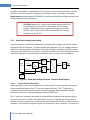
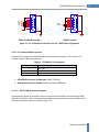
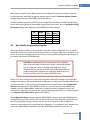
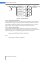
1
Active Front End (AFE) Controller User’s Manual UM-0021 11 Continental Blvd Merrimack NH 03054 v. (603) 546-0090 f. (603)386-6366 oztekcorp.com About Oztek Oztek Corp. is proven innovator of power, control, and instrumentation solutions for the most demanding industrial applications. Oztek products include variable motor drives, grid tie inverters, frequency converters, stand alone inverters, DC/DC converters, and DSP based control boards for power control applications. Trademarks OZDSP3000 is a trademark of Oztek Corp. Other trademarks, registered trademarks, and product names are the property of their respective owners and are used herein for identification purposes only. Notice of Copyright Oztek AFE User’s Manual © December 2010 Oztek Corp. All rights reserved. Exclusion for Documentation UNLESS SPECIFICALLY AGREED TO IN WRITING, Oztek Corp. (“Oztek”) (A) MAKES NO WARRANTY AS TO THE ACCURACY, SUFFICIENCY OR SUITABILITY OF ANY TECHNICAL OR OTHER INFORMATION PROVIDED IN ITS MANUALS OR OTHER DOCUMENTATION. (B) ASSUMES NO RESPONSIBILITY OR LIABILITY FOR LOSSES, DAMAGES, COSTS OR EXPENSES, WHETHER SPECIAL, DIRECT, INDIRECT, CONSEQUENTIAL OR INCIDENTAL, WHICH MIGHT ARISE OUT OF THE USE OF SUCH INFORMATION. THE USE OF ANY SUCH INFORMATION WILL BE ENTIRELY AT THE USER’S RISK. (C) IF THIS MANUAL IS IN ANY LANGUAGE OTHER THAN ENGLISH, ALTHOUGH STEPS HAVE BEEN TAKEN TO MAINTAIN THE ACCURACY OF THE TRANSLATION, THE ACCURACY CANNOT BE GUARANTEED. APPROVED OZTEK CONTENT IS CONTAINED WITH THE ENGLISH LANGUAGE VERSION WHICH IS POSTED AT WWW.OZTEKCORP.COM. Date and Revision October 2013 Rev N Part Number UM-0021 Contact Information USA Telephone: 603-546-0090 Fax: 603-386-6366 Email [email protected] Table of Contents Table of Contents 1. Introduction .................................................................................................................... 1 1.1 1.2 Referenced Documents ............................................................................................................... 1 Definitions ................................................................................................................................... 1 2. Functional Description ..................................................................................................... 2 2.1 Typical Hardware Implementation .............................................................................................. 4 2.1.1 Power Module ......................................................................................................................... 4 2.1.2 Isolation Transformer and Line Filter ...................................................................................... 4 2.1.3 Pre-Charge Circuit ................................................................................................................... 4 2.1.4 Control Board .......................................................................................................................... 5 2.2 Description of Operation ............................................................................................................. 5 2.2.1 DC Link and Current Control Modes ....................................................................................... 5 2.2.2 Operating Modes .................................................................................................................... 5 2.2.3 Stand Alone Voltage Control Mode ........................................................................................ 6 2.2.3.1 Current Overload Protection .......................................................................................... 6 2.3 Dual Interleaved Inverter Operation ........................................................................................... 8 2.4 State Sequencing ......................................................................................................................... 9 2.4.1 Initialize ................................................................................................................................. 10 2.4.2 Calibrate ................................................................................................................................ 11 2.4.3 Precharge .............................................................................................................................. 11 2.4.4 Charge ................................................................................................................................... 11 2.4.5 Idle ......................................................................................................................................... 11 2.4.6 On .......................................................................................................................................... 11 2.4.7 Turn Off ................................................................................................................................. 11 2.4.8 Low DC Link ........................................................................................................................... 11 2.5 Fault and Warning Conditions ................................................................................................... 12 2.5.1 Warnings ............................................................................................................................... 12 2.5.1.1 Inverter High Temperature........................................................................................... 12 2.5.1.2 DC Link High Voltage .................................................................................................... 12 2.5.1.3 DC Link Low Voltage ..................................................................................................... 12 2.5.1.4 PLL Not Locked ............................................................................................................. 12 2.5.1.5 High Inverter Current ................................................................................................... 13 2.5.1.6 Grid Frequency Out of Tolerance ................................................................................. 13 2.5.1.7 Grid Voltage Out of Tolerance ...................................................................................... 13 2.5.1.8 Auxiliary High Temperature.......................................................................................... 13 2.5.1.9 Local Bias Supply Tolerance Warnings ......................................................................... 13 2.5.2 Faults ..................................................................................................................................... 13 2.5.2.1 Inverter Hardware Over-Temperature ......................................................................... 14 2.5.2.2 Inverter IGBT Error ....................................................................................................... 14 2.5.2.3 Precharge Timeout Error .............................................................................................. 14 2.5.2.4 Precharge Contactor Error............................................................................................ 14 2.5.2.5 Grid Contactor Error ..................................................................................................... 14 2.5.2.6 Relay Driver Hardware Error ........................................................................................ 14 2.5.2.7 Communications Timeout ............................................................................................ 15 2.5.2.8 Configuration Memory Error ........................................................................................ 15 2.5.2.9 Software Inverter Over-Temperature .......................................................................... 15 2.5.2.10 Software DC Link Over-Voltage .................................................................................... 15 2.5.2.11 Software DC Link Under-Voltage .................................................................................. 15 Publication UM-0021 i ii Table of Contents 2.5.2.12 2.5.2.13 2.5.2.14 2.5.2.15 2.5.2.16 2.5.2.17 PLL Lost Lock ................................................................................................................. 16 Software Inverter Over-Current ................................................................................... 16 Grid Frequency Fault .................................................................................................... 16 Grid Voltage Fault ......................................................................................................... 16 Software Auxiliary Over-Temperature ......................................................................... 16 Calibration Error ........................................................................................................... 16 3. OZDSP3000 Hardware Interfacing .................................................................................. 16 3.1 Application Interfaces................................................................................................................ 17 3.1.1 J11: SKiiP Power Module Interface – Inverter A ................................................................... 17 3.1.2 Custom Driver Interface Considerations ............................................................................... 18 3.1.2.1 Power............................................................................................................................ 19 3.1.2.2 Switch Commands ........................................................................................................ 19 3.1.2.3 Error Inputs ................................................................................................................... 19 3.1.2.4 DC Link Voltage Sensing ............................................................................................... 19 3.1.2.5 DC Link Hardware Over-Voltage Protection ................................................................. 19 3.1.2.6 Hardware Over-Current and Desaturation Protection ................................................. 19 3.1.2.7 Current Sense Signals ................................................................................................... 19 3.1.2.8 Temperature Sense Signals .......................................................................................... 20 3.1.3 J13: SKiiP Power Module Interface – Inverter B (optional) ................................................... 20 3.1.4 J8: Relay Driver Interface ...................................................................................................... 20 3.1.5 J9: Isolated Digital Inputs ...................................................................................................... 21 3.1.6 J10: Isolated Digital Outputs ................................................................................................. 21 3.1.7 J23: High Voltage Line Feedback ........................................................................................... 22 3.1.8 J25: Bias Power Input ............................................................................................................ 23 3.1.9 J4: External Temperature Input ............................................................................................ 23 3.1.10 P1: Isolated Serial Interface .................................................................................................. 24 3.1.10.1 RS232 Configuration ..................................................................................................... 24 3.1.10.2 RS422/485 Configuration ............................................................................................. 24 3.1.11 P2: Isolated CAN Bus Interface.............................................................................................. 25 3.1.11.1 J18/19 CAN Termination Jumpers ................................................................................ 25 3.2 Electrical Interfaces ................................................................................................................... 27 3.3 Mechanical Interface ................................................................................................................. 28 4. Parameter Register Interface ......................................................................................... 29 4.1 Register Properties .................................................................................................................... 29 4.1.1 Parameter ID ......................................................................................................................... 29 4.1.2 Data Types ............................................................................................................................. 29 4.1.2.1 Specifying Fixed-Point Parameters ............................................................................... 29 4.1.3 Access Level........................................................................................................................... 30 4.2 Volatile Registers ....................................................................................................................... 30 4.2.1 Command Registers .............................................................................................................. 30 4.2.1.1 On/Off Control .............................................................................................................. 30 4.2.1.2 Mode Control ............................................................................................................... 30 4.2.1.3 DC Link Voltage Setpoint .............................................................................................. 31 4.2.1.4 Grid Current Setpoint - Real ......................................................................................... 31 4.2.1.5 Grid Current Setpoint - Reactive .................................................................................. 31 4.2.1.6 Power Factor Setpoint .................................................................................................. 31 4.2.1.7 Fault Reset .................................................................................................................... 32 4.2.1.8 Configuration Password ............................................................................................... 32 4.2.1.9 Configuration Reset ...................................................................................................... 32 AFE Controller User’s Manual Table of Contents 4.2.1.10 Configuration Reload .................................................................................................... 33 4.2.1.11 Stand Alone Voltage Setpoint....................................................................................... 33 4.2.1.12 Isolated Digital Output Control .................................................................................... 33 4.2.2 Instrumentation Registers..................................................................................................... 34 4.2.2.1 AFE Operating State ..................................................................................................... 34 4.2.2.2 AFE Operating Mode .................................................................................................... 35 4.2.2.3 DC Link Voltage ............................................................................................................. 35 4.2.2.4 AC Line Voltage ............................................................................................................. 35 4.2.2.5 Grid Current .................................................................................................................. 35 4.2.2.6 AC Line Frequency ........................................................................................................ 35 4.2.2.7 Power Factor ................................................................................................................ 35 4.2.2.8 PLL Status...................................................................................................................... 35 4.2.2.9 Inverter A Temperature................................................................................................ 35 4.2.2.10 Auxiliary Temperature .................................................................................................. 36 4.2.2.11 Contactor Status ........................................................................................................... 36 4.2.2.12 Warning Status ............................................................................................................. 36 4.2.2.13 Fault Status ................................................................................................................... 36 4.2.2.14 Register Operation Status ............................................................................................ 37 4.2.2.15 DSP Software Revision – Major/Minor ......................................................................... 38 4.2.2.16 FPGA Firmware Revision – Major/Minor ..................................................................... 38 4.2.2.17 Board Hardware Revision ............................................................................................. 38 4.2.2.18 Inverter A/B Current ..................................................................................................... 38 4.2.2.19 Inverter B Temperature ................................................................................................ 38 4.2.2.20 Fault Status2 ................................................................................................................. 38 4.2.2.21 Isolated Digital Input Status ......................................................................................... 38 4.3 Non-Volatile Configuration Registers ........................................................................................ 39 4.3.1 Configuration Control Parameters ........................................................................................ 40 4.3.1.1 EEPROM Header ........................................................................................................... 40 4.3.1.2 Factory Configuration Revision – Major ....................................................................... 41 4.3.1.3 Factory Configuration Revision – Minor ....................................................................... 41 4.3.1.4 Application Configuration Data Revision...................................................................... 41 4.3.1.5 Hardware Configuration ............................................................................................... 41 4.3.1.6 User Configuration Revision ......................................................................................... 41 4.3.1.7 Configuration Password ............................................................................................... 42 4.3.2 CAN Interface Parameters..................................................................................................... 42 4.3.2.1 CAN Automatic Alarm Transmit Enable........................................................................ 42 4.3.2.2 CAN Timeout................................................................................................................. 43 4.3.2.3 CAN Group ID................................................................................................................ 43 4.3.2.4 CAN Module ID ............................................................................................................. 43 4.3.2.5 CAN Baud Rate.............................................................................................................. 43 4.3.2.6 CAN Status Destination Group ID ................................................................................. 43 4.3.2.7 CAN Status Destination Module ID............................................................................... 43 4.3.2.8 CAN Update Rate – DC Link Status Message ................................................................ 44 4.3.2.9 CAN Update Rate – Grid Voltage Status Message ........................................................ 44 4.3.2.10 CAN Update Rate – Inverter Current Status Message.................................................. 44 4.3.2.11 CAN Update Rate – Grid Status Message ..................................................................... 44 4.3.2.12 CAN Update Rate – System Status Message ................................................................ 44 4.3.2.13 CAN Update Rate - Alarm Status Message ................................................................... 44 Publication UM-0021 iii iv Table of Contents 4.3.2.14 CAN Broadcast Message Receive Enable ..................................................................... 44 4.3.2.15 CAN Update Rate - Alarm 2 Status Message ................................................................ 45 4.3.3 System Measurement Scaling Parameters ........................................................................... 45 4.3.3.1 DC Link Voltage Measurement – Full Scale .................................................................. 45 4.3.3.2 Line Voltage Measurement – Full Scale ....................................................................... 45 4.3.3.3 Inverter Current Measurement – Full Scale ................................................................. 45 4.3.3.4 Inverter Current Measurement – Polarity Select ......................................................... 46 4.3.3.5 Inverter Current Measurement Auto Calibration......................................................... 46 4.3.4 Default Operating Parameters .............................................................................................. 46 4.3.4.1 Default Control Mode................................................................................................... 46 4.3.4.2 Default Voltage Setpoint .............................................................................................. 46 4.3.4.3 Default Real Current Setpoint ...................................................................................... 47 4.3.4.4 Default Reactive Current Setpoint................................................................................ 47 4.3.4.5 Voltage Mode Current Limit Max ................................................................................. 47 4.3.4.6 Voltage Mode Current Limit Min.................................................................................. 47 4.3.4.7 Default Power Factor Setpoint ..................................................................................... 47 4.3.4.8 Default Stand Alone Voltage Setpoint .......................................................................... 48 4.3.5 Grid Monitor and Protection Parameters ............................................................................. 48 4.3.5.1 Grid Fast/Slow Over/Under Voltage Thresholds and Clear Times ............................... 48 4.3.5.2 Grid Fast/Slow Over/Under Frequency Thresholds and Clear Times ........................... 49 4.3.5.3 Grid Reconnect Delay Time .......................................................................................... 49 4.3.6 Fault and Warning Parameters ............................................................................................. 49 4.3.6.1 DC Link Over-Voltage Fault Threshold.......................................................................... 49 4.3.6.2 DC Link Over-Voltage Warning Threshold .................................................................... 50 4.3.6.3 DC Link Over-Voltage Recover Threshold..................................................................... 50 4.3.6.4 Grid Over-Current Fault Threshold ............................................................................... 50 4.3.6.5 Grid Over-Current Warning Threshold ......................................................................... 50 4.3.6.6 Grid Over-Current Recover Threshold.......................................................................... 50 4.3.6.7 Inverter Temperature Fault Threshold ......................................................................... 50 4.3.6.8 Inverter Temperature Warning Threshold ................................................................... 50 4.3.6.9 Inverter Temperature Recover Threshold .................................................................... 51 4.3.6.10 Auxiliary Temperature Fault Threshold ........................................................................ 51 4.3.6.11 Auxiliary Temperature Warning Threshold .................................................................. 51 4.3.6.12 Auxiliary Temperature Recover Threshold ................................................................... 51 4.3.6.13 Inverter Error Pin Active High ....................................................................................... 51 4.3.6.14 Inverter Over Temp Pin Active High ............................................................................. 51 4.3.6.15 DC Link Under-Voltage Fault Threshold ....................................................................... 51 4.3.6.16 DC Link Under-Voltage Warning Threshold.................................................................. 51 4.3.6.17 DC Link Under-Voltage Recover Threshold .................................................................. 51 4.3.7 Converter Control Parameters .............................................................................................. 52 4.3.7.1 Pulse Width Modulation Frequency ............................................................................. 52 4.3.7.2 Pulse Width Modulation Deadband Enable ................................................................. 52 4.3.7.3 Pulse Width Modulation Deadband Time .................................................................... 52 4.3.7.4 Pulse Width Modulation Max/Min Duty Cycle ............................................................. 52 4.3.7.5 Pulse Width Modulation Action ................................................................................... 53 4.3.7.6 Grid Voltage Line Sensing Select .................................................................................. 53 4.3.7.7 Automatic Grid Fault Recovery..................................................................................... 53 4.3.7.8 Use Power Factor Setpoint ........................................................................................... 54 AFE Controller User’s Manual Table of Contents 4.3.7.9 Total Line Filter Inductance .......................................................................................... 54 4.3.7.10 Nominal Grid Frequency............................................................................................... 54 4.3.7.11 Inverter Power Stage Dead Time.................................................................................. 54 4.3.7.12 Output Modulation Type .............................................................................................. 54 4.3.7.13 Hardware On/Off Pin Control ....................................................................................... 55 4.3.8 Inverter Temperature Monitor Parameters .......................................................................... 55 4.3.8.1 Inverter Temp Coefficients (C0 through C3)................................................................. 55 4.3.9 Auxiliary Temperature Monitor Parameters ......................................................................... 56 4.3.9.1 Auxiliary Temperature Sensor Enable .......................................................................... 56 4.3.9.2 Auxiliary Temp Coefficients (C0 through C3)................................................................ 56 4.3.10 Voltage Regulator Parameters .............................................................................................. 57 4.3.10.1 Voltage Command Slew Limit....................................................................................... 57 4.3.10.2 Voltage Controller Gain Constants (Kp, Ki)................................................................... 57 4.3.10.3 Voltage Droop Control Gain (Kdroop) .............................................................................. 58 4.3.11 Current Regulator Parameters .............................................................................................. 58 4.3.11.1 Current Command Slew Rate ....................................................................................... 58 4.3.11.2 Current Controller Gain Constants (Kp, Ki)................................................................... 59 4.3.11.3 Turn Off Current Slew Rate .......................................................................................... 59 4.3.11.4 Iq Current Command Offset ......................................................................................... 59 4.3.11.5 Nominal DC Link ........................................................................................................... 60 4.3.12 Phase Lock Loop (PLL) Parameters ........................................................................................ 60 4.3.12.1 PLL Controller Gain Constants (Kp/Ki, Locked/Unlocked) ............................................ 60 4.3.12.2 PLL Output Range ......................................................................................................... 61 4.3.12.3 PLL Phase Detector Error Threshold ............................................................................. 61 4.3.12.4 PLL Lock Indicator AC Line Count ................................................................................. 61 4.3.12.5 PLL Unlock Indicator AC Line Count.............................................................................. 61 4.3.12.6 PLL Phase Lag Adjustment ............................................................................................ 61 4.3.12.7 PLL Phase Error LPF Cutoff Frequency .......................................................................... 61 4.3.12.8 PLL Auto Gain Control Filter Constant .......................................................................... 61 4.3.12.9 PLL Capacitor Sensing Adjustment ............................................................................... 61 4.3.13 Pre-charge Parameters.......................................................................................................... 62 4.3.13.1 DC Link Pre-charge Enable ............................................................................................ 62 4.3.13.2 DC Link Pre-charge Threshold ...................................................................................... 62 4.3.13.3 Contactor Debounce..................................................................................................... 62 4.3.13.4 Contactor Close Time ................................................................................................... 62 4.3.13.5 Precharge Timeout Threshold ...................................................................................... 62 4.3.13.6 Contactor Monitor Enables .......................................................................................... 63 4.3.13.7 Grid Contactor Enable .................................................................................................. 63 4.3.14 Instrumentation Parameters ................................................................................................. 63 4.3.14.1 Instrumentation Interrupt Rate .................................................................................... 63 4.3.14.2 Low Pass Cutoff Freq – V DC Link Instrumentation ...................................................... 64 4.3.14.3 Low Pass Cutoff Freq – V DC Link Feedback ................................................................. 64 4.3.14.4 Low Pass Cutoff Freq – Grid Voltage ............................................................................ 64 4.3.14.5 Low Pass Cutoff Freq – Grid Current ............................................................................ 64 4.3.14.6 Low Pass Cutoff Freq – Grid Frequency........................................................................ 64 4.3.14.7 Low Pass Cutoff Freq – Temperatures.......................................................................... 64 4.3.14.8 Low Pass Cutoff Freq – Grid Voltage Feedforward ...................................................... 64 4.3.15 Dual Interleaved Inverter Parameters .................................................................................. 64 Publication UM-0021 v vi Table of Contents 4.3.15.1 Dual Interleaved Inverter Enable.................................................................................. 64 4.3.15.2 Zero Sequence Current Control Enable ........................................................................ 65 4.3.15.3 Zero Sequence Current Controller Gain Constants (Kp, Ki) .......................................... 65 4.3.16 Modbus Parameters .............................................................................................................. 66 4.3.16.1 Modbus Address ........................................................................................................... 66 4.3.16.2 Modbus Baud Rate ....................................................................................................... 66 4.3.16.3 Modbus Parity .............................................................................................................. 66 4.3.17 Stand Alone Voltage Regulator Parameters.......................................................................... 67 4.3.17.1 Voltage Resonant Controller Gain & Phase Constants ................................................. 67 4.3.17.2 Voltage Command Slew Limit....................................................................................... 68 4.3.17.3 High Pass Filter Coefficients ......................................................................................... 68 4.3.18 Current Overload Protection Parameters ............................................................................. 69 4.3.18.1 Rated RMS Current ....................................................................................................... 69 4.3.18.2 I2T Trip Time.................................................................................................................. 69 4.3.18.3 10-100% RMS Overload Trip Times .............................................................................. 69 5. Oztek PCC Tool............................................................................................................... 70 6. Maintenance and Upgrade ............................................................................................. 70 7. APPENDIX A – 100kW Reference Design and Performance Data...................................... 71 7.1 7.2 7.3 Overview .................................................................................................................................... 74 Current Mode Performance ...................................................................................................... 74 Voltage Mode Performance ...................................................................................................... 76 Warranty and Product Information ...................................................................................... 78 Return Material Authorization Policy ................................................................................... 80 AFE Controller User’s Manual Table of Contents Table of Figures Figure 1 – Typical Renewable Energy PV Solar Application .......................................................................... 3 Figure 2 – Typical Regenerative Motor Drive Application ............................................................................ 3 Figure 3 – Typical Turbo-Alternator Application with Stand Alone Voltage Mode Capability ..................... 3 Figure 4 – Typical AFE Electrical System Schematic ...................................................................................... 4 Figure 5 – AFE Controller Functional Block Diagram .................................................................................... 5 Figure 6 – Stand Alone Voltage Controller Functional Block Diagram.......................................................... 6 Figure 7 – Stand Alone Mode I2∙T Protection Characteristic ........................................................................ 7 Figure 8 – Stand Alone Mode RMS Protection Characteristic ...................................................................... 7 Figure 9 – Typical Interleaved AFE Electrical System Schematic .................................................................. 8 Figure 10 – Interleaved AFE Controller Functional Block Diagram ............................................................... 9 Figure 11 – System State Machine.............................................................................................................. 10 Figure 12 – OZDSP3000 AFE Application Electrical Connections ................................................................ 17 Figure 13 – P1: Isolated Serial Interface Pin-out - RS232 Configuration .................................................... 24 Figure 14 – P1: Isolated Serial Interface Pin-out - RS422/485 Configuration ............................................. 25 Figure 15 – Multi-Node CAN Network Configuration ................................................................................. 26 Figure 16 – CAN Interface Circuit ................................................................................................................ 26 Figure 17 – Approximate Connector, Jumper, LED, and Test Hook Locations............................................ 27 Figure 18 – OZDSP3000 Mechanical Dimensions ....................................................................................... 28 Figure 19 – Voltage Control PI Regulator.................................................................................................... 57 Figure 20 – Current Control PI Regulators .................................................................................................. 59 Figure 21 – Zero Sequence PI Regulator ..................................................................................................... 65 Figure 22 – Resonant Controller ................................................................................................................. 68 Figure 23 – Current Mode Normal Operation, 120A .................................................................................. 75 Figure 24 – Current Mode Turn-On, Islew = 300A/s (left) and 1200A/s (right) ............................................ 75 Figure 25 – Voltage Mode Turn-On, Vslew = 1500V/s (left) and 5000V/s (right) ......................................... 76 Figure 26 – Voltage Mode Transient Response .......................................................................................... 77 Figure 27 – Voltage Mode Transient Response (Faster) ............................................................................. 77 Publication UM-0021 vii viii Table of Contents Table of Tables Table 1 – J11 SKiiP Power Module Pin Assignment .................................................................................... 18 Table 2 – J11 Current Sense Pin Assignment .............................................................................................. 20 Table 3 – J8 Relay Drive Pin Assignment ..................................................................................................... 20 Table 4 – J9 Isolated Digital Input Pin Assignment ..................................................................................... 21 Table 5 – J10 Isolated Digital Output Pin Assignment ................................................................................ 22 Table 6 – J23 High Voltage Sense Pin Assignment ...................................................................................... 22 Table 7 – J12 RS-485 Pin Assignment.......................................................................................................... 23 Table 8 – J4 Pin Assignment ........................................................................................................................ 23 Table 9 – J15 RS422/485 Configuration Jumper Settings ........................................................................... 24 Table 10 – P2 CAN Bus Pin Assignment ...................................................................................................... 25 Table 11 – Command Register Set .............................................................................................................. 30 Table 12 – Instrumentation Register Set .................................................................................................... 34 Table 13 – Configuration Control Parameter Summary ............................................................................. 40 Table 14 – CAN Interface Parameter Summary .......................................................................................... 42 Table 15 – System Measurement Scaling Parameter Summary ................................................................. 45 Table 16 – Default Operating Parameter Summary ................................................................................... 46 Table 17 – Fault and Warning Parameter Summary ................................................................................... 48 Table 18 – Fault and Warning Parameter Summary ................................................................................... 49 Table 19 – Converter Control Parameter Summary ................................................................................... 52 Table 20 – Inverter Temperature Parameter Summary ............................................................................. 55 Table 21 – Auxiliary Temperature Parameter Summary ............................................................................ 56 Table 22 – Voltage Regulator Parameter Summary ................................................................................... 57 Table 23 – Current Regulator Parameter Summary ................................................................................... 58 Table 24 – PLL Control Parameter Summary .............................................................................................. 60 Table 25 – Pre-charge Parameter Summary ............................................................................................... 62 Table 26 – Instrumentation Parameter Summary ...................................................................................... 63 Table 27 – Instrumentation Parameter Summary ...................................................................................... 64 Table 28 – Modbus Parameter Summary ................................................................................................... 66 Table 29 – Stand Alone Voltage Regulator Parameter Summary ............................................................... 67 Table 30 – Current Overload Protection Parameter Summary .................................................................. 69 Table 31 – Current Mode THD .................................................................................................................... 74 Table 32 – Voltage Mode THD .................................................................................................................... 76 AFE Controller User’s Manual Introduction 1. Introduction This document is intended to provide instruction on how to employ the Oztek AFE firmware application on a standard Oztek OZDSP3000 controller in an actual hardware system. It describes the electrical connections as well as the scaling of the various signals required by the control firmware. 1.1 Referenced Documents Ref. Document Description [1] [2] [3] [4] [5] [6] UM-0018 FS-0046 FS-0047 FS-0053 UM-0015 UM-0036 OZDSP3000 Users Manual OzCan Protocol Function Specification OzCan AFE Device Profile Modbus Protocol Functional Specification Oztek TMS28x CAN Bootloader Users Manual Power Control Center GUI User’s Manual 1.2 Definitions AFE CAN DSP EEPROM EMC EMI GND GTI GUI HMI IPM N.C. PCB PCC PI PLC PLL POR PWM SVM Active Front End Controller Area Network Digital signal processor Electrically Erasable Programmable Read Only Memory Electro-magnetic compatibility Electro-magnetic interference Ground, low side of input power supply Grid Tied Inverter Graphical User Interface Human Machine Interface Intelligent Power Module Not connected Printed Circuit Board Power Control Center Proportional and Integral Compensator Programmable Logic Controller Phase Locked Loop Power On Reset Pulse width modulation Space Vector Modulator Publication UM-0021 1 2 Functional Description 2. Functional Description An Active Front End (AFE) is used to transfer power between an AC power input and an intermediate DC circuit or Link. It generally has the ability to transfer power in both directions, operating as a rectifier when transferring power from the AC line to the DC link and as an inverter in the opposite direction. AFEs provide very low current distortion (THDI) when compared to other front end rectifier solutions. Advantages of the OzAFE solutions include: Low AC Input Harmonics – The OzAFE controller provides low harmonic distortion to meet IEEE-519 at the AC line inputs. Improved Power Factor – The OzAFE controller provides power factor correction resulting in unity power factor operation for energy savings and system efficiency. Voltage Boost Capability – The pulse width modulated control scheme behaves as a boost regulator, providing regulated DC voltages higher than the rectified AC line. This isolates the load electronics from the effects of AC line voltage sags. Regenerative Capability – OzAFE based applications achieve considerable savings in terms of power savings and the related costs. The ability to transfer power from the DC link to the AC line provides a direct interface with regenerative loads, transforming the kinetic energy of the inertial loads into electrical energy. This eliminates the need for braking resistors and saves the wasted energy, instead returning it to the line to be used by other equipment. Stand-Alone Voltage Mode Capability – The OzAFE controller also provides the ability to operate the converter in “Stand Alone” Voltage Mode. In this mode the inverter can be configured to produce a controlled AC output voltage. This is useful in grid tie applications that require the converter to be able to produce “standby” power when the utility is down. ATTENTION: While the AFE can be used for voltage boost, it cannot be used to lower the DC link voltage. The minimum DC link voltage is limited by the rectified AC line voltage AFE Controller User’s Manual Functional Description Typical AFE applications include renewable energy systems as well as power systems with high inertial loads such as centrifuges, test benches, rolling systems, high power servo systems, mixers etc. OzBoost 3-Phase 480VAC OzAFE DC+ DC+ DC+ DC- DC- DC- L1 PV L2 L3 Figure 1 – Typical Renewable Energy PV Solar Application 3-Phase 480VAC OzAFE L1 DC+ L2 DC- L3 - + - + Inverter 1 Inverter 2 M - + Inverter 3 M M Figure 2 – Typical Regenerative Motor Drive Application OzAFE L1 A Switch Gear OzAFE DC+ DC+ DC- DC- 3-Phase 480VAC L1 L2 L2 L3 L3 Loads Figure 3 – Typical Turbo-Alternator Application with Stand Alone Voltage Mode Capability Publication UM-0021 3 4 Functional Description 2.1 Typical Hardware Implementation Figure 4 illustrates a typical AFE electrical system implementation. While component values will vary from application to application depending on line voltage and power level, the overall system configuration will generally remain the same. Pre-Charge Circuitry K1 DC+ K2 EMI Filter DC- 480VAC Grid 24V Relay Power Stage Interface 24V Relay Precharge Relay Drive Line Interface Relay Drive 24V DC Precharge RelayStatus Line Interface Relay Status Control Board CAN Line Voltage Phase A Line Voltage Phase B Line Voltage Phase C Figure 4 – Typical AFE Electrical System Schematic 2.1.1 Power Module The power module is a three phase semiconductor bridge which controls the power transfer from the AC Line to the DC link and vice versa. Oztek control boards are designed to interface directly with Semikron SKiiP power modules. In addition to the power devices, these modules provide current sensing, DC link voltage sensing, temperature sensing, and protection features including over voltage, over current, and de-saturation protection. 2.1.2 Isolation Transformer and Line Filter An isolation transformer is used to provide isolation between the AFE and the utility. In addition, it is usually included in the design of the line filter used to remove the high frequency switching harmonics from the line current. An L-C-L filter architecture is typically employed with damping provided by series resistive elements. 2.1.3 Pre-Charge Circuit A pre-charge circuit is used to limit the inrush current associated with charging the DC link capacitance when applying line voltage to the AFE. Lack of a pre-charge circuit can result in extremely high, potentially damaging inrush currents. AFE Controller User’s Manual Functional Description 2.1.4 Control Board The control board is used to generate the gating signals to the power switches in order to control either line current or DC link voltage. The control board also provides instrumentation and user control functions. 2.2 Description of Operation 2.2.1 DC Link and Current Control Modes Figure 5 presents a simplified block diagram of the control scheme employed in the AFE firmware. The DC link voltage controller is a PI type regulator whose reference sets the value of the DC link voltage to be maintained. This reference is compared to the measured DC link voltage providing the DC voltage error input to the PI regulator. The output of the DC link voltage controller serves as the active current reference while the reactive current reference is used to maintain power factor. PI regulators are used to control both the active and reactive current components using current feedback calculated from the three phase current measurements (ILa, ILb, ILc). The current regulators are implemented in the voltage-oriented synchronous DQ reference frame. A digital phase locked loop (PLL) provides synchronization with the AC line voltage. The outputs of the active and reactive PI regulators are then used to control a space vector modulator (SVM) which generates the gating commands to the power switches. Space vector operation may optionally be disabled and replaced with sine wave modulation (see PID 0x806C). Iref OpMode Current Controller Vref Vdc Iactive PI dq iLabc Voltage Controller abc Ireactive id PI v*d abc v*abc iq PI SVM PWM v*q dq q PLL vLabc Figure 5 – AFE Controller Functional Block Diagram 2.2.2 Operating Modes Typically, an AFE is used to regulate the DC link voltage as previously described. In order to maintain the desired DC link voltage, the voltage regulator will “command” an active current either into or out of the AC line as necessary. In certain applications, there may be a separate Publication UM-0021 5 6 Functional Description controller responsible for regulating the DC link, in which case it may be desirable to operate the AFE as a current controller as opposed to a voltage controller. By properly setting the Mode Control command register (PID 0x0001), the user may disable the voltage controller and directly command the active current. CAUTION: Operation in current control mode assumes there is an external means to control the DC link voltage. DC link voltage control is absolutely necessary when commanding currents into the AFE. Lack of control can result in catastrophic over voltage conditions on the DC link. 2.2.3 Stand Alone Voltage Control Mode Figure 6 presents a simplified block diagram of the stand alone voltage mode control scheme employed in the AFE firmware. A reference angle and quadrature (), AC voltage reference waveforms are generated by the software. The output voltage is sensed by the A/D converter and converted to quadrature () format. Resonant controllers are then employed to provide closed loop regulation by controlling the modulation index of a space vector modulator. Valpha Sine Gen VLabc abc Vbeta V Resonant Controller v* abc v*abc V Resonant Controller v* SVM PWM q Angle Generator Figure 6 – Stand Alone Voltage Controller Functional Block Diagram 2.2.3.1 Current Overload Protection When operating in stand-alone voltage control mode the AFE firmware provides two types of current overload protection, fast I2∙T limit and a slower RMS limit. The I2∙T algorithm is intended to protect the inverter for gross overloads exceeding 200% rated while the RMS protection functions for overloads between rated and 200% rated. The I2∙T algorithm integrates the sample by sample difference between the absolute value of the current waveform and the overload threshold. As such it integrates up during the time when the current is greater than the threshold and down while the waveform is lower than the threshold. If the function integrates beyond a trip threshold, a fault is asserted. The function is AFE Controller User’s Manual Functional Description configured by setting the desired trip time for a 110% overload, i.e. 210% rated output current. The following figure illustrates the time to trip as a function of % overload. Figure 7 – Stand Alone Mode I2∙T Protection Characteristic The RMS algorithm works similarly in that it integrates the difference between the RMS load current and the rated output current. If the function integrates beyond a trip threshold, a fault is asserted. The function is configured by setting the desired trip time for ten overload conditions, 10, 20, 30, 30, 50, 60, 70, 80, 90, and 100% overload. The following figure illustrates the time to trip as a function of % overload. Figure 8 – Stand Alone Mode RMS Protection Characteristic Publication UM-0021 7 8 Functional Description 2.3 Dual Interleaved Inverter Operation The AFE controller provides support for an optional second inverter interface to be used when driving a dual interleaved inverter power stage. Note that this option is not available if the controller is intended to be operated in Stand Alone voltage mode. This system would look very similar to the single inverter system shown in Figure 4 with the addition of a second IGBT bridge and inverter-side filter inductors as shown in the figure below. DC+ Pre-Charge Circuitry K1 Power Stage Interface A K2 EMI Filter 480VAC Grid 24V Relay DC- 24V Relay Power Stage Interface B Precharge Relay Drive Line Interface Relay Drive 24V DC Precharge RelayStatus Line Interface Relay Status Control Board CAN Line Voltage Phase A Line Voltage Phase B Line Voltage Phase C Figure 9 – Typical Interleaved AFE Electrical System Schematic From a control perspective, when operating in dual interleaved inverter mode the OzAFE controller uses the same control scheme as with a single inverter with the addition of a second current controller and PWM modulator. The commanded current is generated the same as the single inverter mode and is then divided by two and sent to each of the two internal current controllers. With this scheme each inverter is handling 50% of the overall load. The PWM pulses on the second inverter use the exact same frequency as the main inverter but are phase shifted by 180 degrees to achieve the desired current ripple cancellation benefit provided by the interleaved system. Additionally, to prevent a circulating DC current from developing between the two inverters, the controller also uses a PI compensator to regulate the DC current to zero in each inverter. This interleaved control scheme is illustrated in the following figure. AFE Controller User’s Manual Functional Description Current Controller B 0 Iref Vref Vdc OpMode Σ Iactive iz 1/2 PI dq iLabc Voltage Controller id PI PI iq Σ dq iz id SVM Σ SVM PWM - INVB v*q dq PI PI v*z v*d abc v*abc A abc Σ Current Controller A 0 iq PI 1/2 abc v*abc PI Ireactive v*d B abc iLabc v*z PWM - INVA v*q dq q PLL vLabc Figure 10 – Interleaved AFE Controller Functional Block Diagram 2.4 State Sequencing A state machine is used to provide deterministic control and sequencing of the AFE hardware. If a fault is detected in any of the operating states, the hardware is placed into a safe condition and the state machine is latched into the Fault state. Figure 11 illustrates the operating states as well as the transition logic employed in the system state machine. Publication UM-0021 9 10 Functional Description POR Initialize Fault Detected Initialization Complete Fault Detected Calibrate Fault Reset & Cal Not Complete Cal Complete Line out of Spec Fault Reset & Cal Complete PreCharge Fault Detected Fault Detected Fault Line OK Charge Fault Detected Fault Detected DC Link Charged Line out of Spec or Mode Change from Stand Alone Stand Alone Mode On Command On Idle Off Command (voltage or stand alone mode) Low DC Link Mode Change from Stand Alone (standalone mode) Off Command (current mode) Fault Detected Turn Off Current Reaches Zero Good DC Link Low DC Link Fault Detected Figure 11 – System State Machine 2.4.1 Initialize The state machine resets to the Initialize state following a power-on-reset (POR) event. While in this state the power hardware is not operable; the firmware is initializing hardware peripherals, configuring variables, and performing self health tests. Upon successful initialization the state machine will auto-transition to the Calibrate state. AFE Controller User’s Manual Functional Description 2.4.2 Calibrate The Calibrate state is used to calibrate system hardware as applicable. Power hardware is not operable while in the Calibrate state. Following successful calibration, the state machine will auto-transition to the Precharge state. 2.4.3 Precharge The Precharge state is used to wait for a valid AC line interface before attempting to begin the DC link charging process. As long as the operating mode is not stand alone voltage mode, the state machine will remain in the Precharge state indefinitely, transitioning either on a fault or upon detecting a valid AC line. Power hardware is not operable while in the Precharge state. If stand alone voltage mode is selected, the state machine will transition directly to the Idle state. 2.4.4 Charge The Charge state is used to charge the DC link capacitance in a controlled manner before directly connecting to the AC line. Once the DC link is charged, the state machine will sequence to the Idle state. Power hardware is not operable while in the Charge state. 2.4.5 Idle Once in the Idle state the AFE is ready for use. The state machine will remain in the Idle state indefinitely, transitioning either on a fault, a turn-on command, or upon detecting an invalid AC line. If the operating mode is switched from stand alone to either DC Link voltage regulation mode or current regulation mode the state machine will transition back to the Precharge state. 2.4.6 On While in the On state the AFE is processing power and controlling either the AC line current or the DC link voltage, depending on the configuration. The state machine will remain in the On state indefinitely, transitioning either on a fault or a turn-off command. When a turn-off command is received, the state machine will immediately go to the Idle state if in voltage regulation mode or to the Turn Off state if in current regulation mode. 2.4.7 Turn Off The Turn Off state is only used when the AFE is operating in current regulation mode and was commanded to turn off. This state is used to wait for the current to ramp down to zero based on the user-specified rate set in the Turn Off Current Slew Rate configuration register (PID 0x8093). Once the current reaches zero the state machine will then transition to the Idle state. 2.4.8 Low DC Link If the controller is in the Idle state and configured for stand alone operation, the state machine will transition to this Low DC Link state if the measured DC link voltage falls below the value Publication UM-0021 11 12 Functional Description specified in the DC Link Under-Voltage Fault Threshold configuration register (PID 0x8111). It will wait in this state until the DC link rises above this fault threshold, at which point it will transition back to the Idle state. If the mode is changed from stand alone to grid tie operation, the state machine will transition back to the Precharge to wait for a valid AC line and to perform DC link precharge if necessary. 2.5 Fault and Warning Conditions The AFE provides warning indicators and fault protection in the event of conditions that may cause damage to the equipment or injure personnel. The various conditions that are monitored by the AFE are listed and described in the following sections. 2.5.1 Warnings The AFE provides the warning indicators listed below. These warning conditions do not prohibit operation of the AFE; they are merely reported for informational purposes only. Each warning condition described below is reported in the Warning Status instrumentation register (PID 0x400F) and also reported on the CAN bus in the Alarm Status CAN message. 2.5.1.1 Inverter High Temperature The AFE firmware monitors the main Inverter A temperature and will set a warning flag if it exceeds the Inverter Temperature Warning Threshold configuration parameter (PID 0x8057). If the Dual Interleaved Inverters Enable configuration parameter (PID 0x80D0) is set to TRUE, the AFE firmware will also monitor the secondary Inverter B temperature and compare this to the same warning threshold value. These flags will remain set until the temperature(s) falls below the Inverter Temperature Recover Threshold configuration parameter (PID 0x8058). 2.5.1.2 DC Link High Voltage The AFE firmware monitors the DC link voltage and will set a warning flag if it exceeds the DC Link Over-Voltage Warning Threshold configuration parameter (PID 0x8051). This flag will remain set until the voltage falls below the DC Link Over-Voltage Recover Threshold configuration parameter (PID 0x8052). 2.5.1.3 DC Link Low Voltage The AFE firmware monitors the DC link voltage and will set a warning flag if it falls below the DC Link Under-Voltage Warning Threshold configuration parameter (PID 0x8112). This flag will remain set until the voltage rises above the DC Link Under-Voltage Recover Threshold configuration parameter (PID 0x8113). 2.5.1.4 PLL Not Locked The AFE firmware monitors the status of the phase lock loop (PLL) module that is providing synchronization to the AC line. The AFE will set a warning flag if the PLL is not locked. This flag is cleared when the PLL regains lock. AFE Controller User’s Manual Functional Description 2.5.1.5 High Inverter Current The AFE firmware monitors the RMS inverter currents for each of the three phases and will set a flag (one per phase) if the current exceeds the Grid Over-Current Warning Threshold configuration parameter (PID 0x8054). It does this for both the main Inverter A and the secondary Inverter B if the Dual Interleaved Inverters Enable configuration parameter (PID 0x80D0) is set to TRUE. These flags remain set until the respective current falls below the Grid Over-Current Recover Threshold configuration parameter (PID 0x8055). 2.5.1.6 Grid Frequency Out of Tolerance The AFE monitors the AC line and will set a warning flag if the frequency is not within the tolerances described in section 4.3.5.2. This is considered a warning condition only if the AFE is presently not ON. The warning flag will be cleared once the grid frequency is within the required limits. 2.5.1.7 Grid Voltage Out of Tolerance The AFE firmware monitors the three RMS Phase-to-Phase Voltages of the utility grid. It will set a warning flag (one per phase-to-phase voltage) if the voltage is not within the tolerances described in section 4.3.5.1. This is considered a warning condition only if the AFE is presently not ON. The warning flags are cleared once the associated voltage is within the required limits. 2.5.1.8 Auxiliary High Temperature If the Auxiliary Temperature Sensor Enable parameter (PID 0x8078) is set to TRUE, the AFE firmware will monitor the external temperature sensor and will set a warning flag if the temperature exceeds the Auxiliary Temperature Warning Threshold configuration parameter (PID 0x805A). This flag will remain set until the temperature falls below the Auxiliary Temperature Recover Threshold configuration parameter (PID 0x805B). 2.5.1.9 Local Bias Supply Tolerance Warnings The AFE firmware monitors the local bias supplies (24V, 15V, 5V, 3.3V, and -15V) on the control board and will set a warning flag if the corresponding supply voltage is not within the range required by the on-board hardware. The various warning flags will remain set while the supply voltages are out of tolerance and will be cleared when the supply is found to be within the required limits. 2.5.2 Faults The AFE provides the fault protection listed below. Whenever a fault occurs the AFE will automatically turn the converter OFF, open the main line contactor and transition to the FAULT state. Each fault condition is latched and reported in the Fault Status instrumentation register (PID 0x4010) and also reported on the CAN bus in the Alarm Status CAN message. The controller remains in the FAULT state and the latched fault flags remain set until explicitly reset with a Fault Reset command (PID 0x0006). This is true even if the source(s) of the fault(s) are no longer active. Upon receiving the Fault Reset command, the AFE will attempt to clear all latched fault bits. It then examines the sources of all fault conditions and if none are active the Publication UM-0021 13 14 Functional Description AFE controller will transition to the Precharge state and attempt to reconnect to the grid. If upon re-examination any sources of faults are still active, their respective fault flags are latched again and the AFE will remain in the FAULT state. The AFE may be optionally configured to automatically recover from grid voltage and frequency faults and turn back ON (if previously enabled) as described in section 4.3.5. 2.5.2.1 Inverter Hardware Over-Temperature The AFE firmware provides a means to recognize a hardware-based over-temperature error signal from the main Inverter A interface (as is present on a typical Semikron SKiiP interface). If the Dual Interleaved Inverters Enable configuration parameter (PID 0x80D0) is set to TRUE, the AFE firmware will also monitor the over-temperature signal from the secondary Inverter B interface. 2.5.2.2 Inverter IGBT Error The AFE firmware provides a means to recognize a hardware-based IGBT error signal from the main Inverter A interface (as is present on a typical Semikron SKiiP interface). ). If the Dual Interleaved Inverters Enable configuration parameter (PID 0x80D0) is set to TRUE, the AFE firmware will also monitor the error signal from the secondary Inverter B interface. 2.5.2.3 Precharge Timeout Error The AFE Firmware monitors the amount of time spent in the CHARGE State. A fault will be asserted if the DC Link Precharge Enable configuration parameter (PID 0x80B0) is set to TRUE (i.e. the AFE is controlling the precharge function) and the elapsed time exceeds the Precharge Timeout Threshold configuration parameter (PID 0x80B4). 2.5.2.4 Precharge Contactor Error The AFE monitors the status of the precharge contactor feedback signal if the precharge contactor monitor is enabled in the Contactor Monitor Enables configuration parameter (PID 0x80B5). If, after the time specified in the Contactor Debounce Time configuration parameter (PID 0x80B2) has passed, the precharge contactor is not in the state commanded by the AFE, a fault will be asserted. 2.5.2.5 Grid Contactor Error The AFE monitors the status of the main grid contactor feedback signal if the grid contactor monitor is enabled in the Contactor Monitor Enables configuration parameter (PID 0x80B5). If, after the time specified in the Contactor Debounce Time configuration parameter (PID 0x80B2) has passed, this contactor is not in the state commanded by the AFE, a fault will be asserted. 2.5.2.6 Relay Driver Hardware Error The AFE monitors the status of the relay drive circuit on the control board that is used to drive the precharge and main line contactors. This hardware circuit provides the ability to detect open load, short circuit, over-voltage and over-current conditions. A fault is asserted if any of these conditions are reported. AFE Controller User’s Manual Functional Description 2.5.2.7 Communications Timeout If the CAN bus interface is used and the CAN Timeout configuration parameter (PID 0x8011) is set to a non-zero value, the AFE will monitor the amount of time elapsed between received CAN messages. A fault will be asserted if the specified timeout threshold is exceeded. 2.5.2.8 Configuration Memory Error This fault occurs any time a read from the configuration memory is performed and the CRC for the block being read does not match the CRC stored in the memory. This may occur if the data was corrupted in transmission during the read or this may occur if the data stored in memory was corrupted. Unlike all other fault sources, this fault condition is not cleared with the Fault Reset command (PID 0x0006) as the fault condition indicates the possibility that the control parameters are not as intended. Instead, this fault is considered a major system fault and needs to be addressed as follows: 1. Attempt to reload the system configuration using the Configuration Reload command (PID 0x0009) or cycle power to the control board. Either of these actions will reset the CPU on the control board which then forces a re-initialization of the application, including reading the configuration parameters from the external configuration memory. If this completes without error, this implies the previous error occurred while the data was being read. 2. If after executing step 1 above a configuration error is still present, this may indicate bad data in the configuration memory. In this case, the memory will need to be reset to the factory defaults using the Configuration Reset command (PID 0x0008). Once the memory contents have been reset and any values changed to their customized settings, step 1 above should be executed to force a reload of the system variables. 3. If neither of the above result in clearing the configuration error, then there is likely an issue with the control board hardware. At this point the board should be sent back to the factory for diagnosing and repairing of any defects (see the RMA process described at the end of this document). 2.5.2.9 Software Inverter Over-Temperature The AFE monitors the main Inverter A temperature and will assert a fault if it exceeds the Inverter Temperature Fault Threshold configuration parameter (PID 0x8056). ). If the Dual Interleaved Inverters Enable configuration parameter (PID 0x80D0) is set to TRUE, the AFE firmware will also monitor the temperature from the secondary Inverter B interface and check this against the same fault threshold value. 2.5.2.10 Software DC Link Over-Voltage The AFE firmware monitors the DC link voltage and will assert a fault if it exceeds the DC Link Over-Voltage Fault Threshold configuration parameter (PID 0x8050). 2.5.2.11 Software DC Link Under-Voltage The AFE firmware monitors the DC link voltage and will assert a fault if it drops below the DC Link Under-Voltage Fault Threshold configuration parameter (PID 0x8011), while it is ON and operating in Stand Alone voltage mode. Publication UM-0021 15 16 OZDSP3000 Hardware Interfacing 2.5.2.12 PLL Lost Lock The AFE firmware monitors the status of the phase lock loop (PLL) module that is providing synchronization to the AC line. A fault is asserted if the AFE is in the ON state the PLL loses lock. This fault only occurs when the AFE is ON or if an attempt is made to turn the AFE ON when the PLL is not locked. 2.5.2.13 Software Inverter Over-Current The AFE firmware monitors the RMS current for each of the three phases on the main Inverter A and asserts a fault if any phase exceeds the Grid Over-Current Fault Threshold configuration parameter (PID 0x8053). ). If the Dual Interleaved Inverters Enable configuration parameter (PID 0x80D0) is set to TRUE, the AFE firmware will also monitor the currents from the secondary Inverter B interface and check these against the same fault threshold value. 2.5.2.14 Grid Frequency Fault The AFE will assert a fault the measured AC line frequency is not within the tolerances described in section 4.3.5.2. This fault only occurs when the AFE is ON or if an attempt is made to turn the AFE ON. Otherwise this is only reported as a warning condition. 2.5.2.15 Grid Voltage Fault The AFE firmware monitors the three RMS Phase-to-Phase Voltages of the utility grid. A fault is asserted if any of these voltages are not within the tolerances described in section 4.3.5.1. This fault only occurs when the AFE is ON or if an attempt is made to turn the AFE ON. Otherwise this is only reported as a warning condition. 2.5.2.16 Software Auxiliary Over-Temperature If the Auxiliary Temperature Sensor Enable configuration parameter (PID 0x8078) is set to TRUE, the AFE will monitor the external temperature sensor and assert a fault if the temperature exceeds the Auxiliary Temperature Fault Threshold configuration parameter (PID 0x8059). 2.5.2.17 Calibration Error When first powering up the control board the AFE software attempts to calibrate the controller’s internal ADC. This error is asserted if the controller is unable to perform the required calibration. There is likely an issue with the control board hardware if this error occurs, in which case the board should be sent back to the factory for diagnosing and repairing of any defects (see the RMA process described at the end of this document). 3. OZDSP3000 Hardware Interfacing The OZDSP3000 is a highly integrated DSP control solution for power control applications. Typical applications include voltage output inverters, grid-tie inverters, AC induction motor controllers, brushless DC motor controllers, and Active Front-End regulators. This section describes how to utilize the OZDSP3000 along with the AFE control firmware in a typical AFE system application. AFE Controller User’s Manual OZDSP3000 Hardware Interfacing 3.1 Application Interfaces J11 26 pin Ribbon Cable Interface SKiiP Power Module – Inverter A J25 24 VDC 24V RTN 1 5 CANH CANL GND 7 2 3 J13 26 pin Ribbon Cable Interface SKiiP Power Module – Inverter B P2 (optional) L1 J8 L2 L3 3 24VDC 7 J10 FAULT Optional Open-Collector Output Pins DOUT2 DOUT1 DOUT0 24V RTN 8 4 7 3 6 2 5 1 To Inverter Filter OZDSP3000 L1 L2 L3 4 24VDC 8 To Precharge 24VDC Optional Hardware Control Pins On/Off Fault Reset 24V RTN J9 4 8 3 7 J4 External Temp J9 1 2 1 5 2 6 24V RTN 1 4 7 Vline A Vline B Vline C J23 Figure 12 – OZDSP3000 AFE Application Electrical Connections 3.1.1 J11: SKiiP Power Module Interface – Inverter A Connector J11 provides an interface to SKiiP style Semikron power modules. This interface complies with Semikron’s required specifications. The OZDSP3000 supplies 24V power to the power module via pins 14 and 15. PWM commands (15V logic level) are supplied to the top and bottom switches of each of the three half bridges via signals INV_TOP_U(V,W) and INV_BOT_U(V,W) respectively. Feedback of phase currents, temperature, and DC link voltage are provided on INV_IOUT_U(V,W), INV_TEMP, INV_UDC signals respectively. Error signals from the module are similarly provided via INV_ERR_U(V,W) and INV_OVT. Please refer to the Semikron datasheet for the particular module being used for more information. Publication UM-0021 17 18 OZDSP3000 Hardware Interfacing Table 1 – J11 SKiiP Power Module Pin Assignment Pin # 1 2 3 4 5 6 7 8 9 10 11 12 13 14 15 16 17 18 19 20 21 22 23 24 25 26 Description Ground INV_BOT_U (Phase A) INV_ERR_U (Phase A) INV_TOP_U (Phase A) INV_BOT_V (Phase B) INV_ERR_V (Phase B) INV_TOP_V (Phase B) INV_BOT_W (Phase C) INV_ERR_W (Phase C) INV_TOP_W (Phase C) INV_OVR_TEMP n/c INV_UDC 24V 24V n/c n/c Ground Ground INV_TEMP INV_IOUT_U_RTN (Phase A) INV_IOUT_U (Phase A) INV_IOUT_V_RTN (Phase B) INV_IOUT_V (Phase B) INV_IOUT_W_RTN (Phase C) INV_IOUT_W (Phase C) OZDSP3000 Connector Part Number: (AMP) 499922-6 Mating Connector Part Number: (AMP) 1658621-6 Power: 24V @ 1.5A 3.1.2 Custom Driver Interface Considerations When attempting to use the OZDSP3000 AFE controller with a custom designed power stage the hardware must be designed to provide the appropriate signals expected at the J11 interface. Generally some sort of custom printed circuit board will be required to interface the J11 signals to the gate drivers, current sensors, etc. AFE Controller User’s Manual OZDSP3000 Hardware Interfacing 3.1.2.1 Power The OZDSP3000 supplies 24V on J11, pins 14 & 15. This 24Vmay be used to power the electronics on the interface board. The supply is capable of providing 1.5A. 3.1.2.2 Switch Commands The six switching commands are provided on pins 2, 4, 5, 7, 8, and 10. These switch command signals are driven off of the OZDSP3000 at 15V logic level using MC14504B level shifting devices. 3.1.2.3 Error Inputs The OZDSP3000 expects three logic level, error inputs; one associated with each phase, on pins 3, 6, and 9. When active, these inputs cause the AFE firmware to latch the system off into the Fault state. Pull-ups to 3.3V are provided on board and the signals are active high. Depending on the features provided in the custom design, these signals can be used to interface single error sources, multiple protection circuits, or none at all. The custom interface board should drive the pin with an open-collector style circuit. In the case where no protection is provided, the pins should be grounded to disable the faults. 3.1.2.4 DC Link Voltage Sensing The OZDSP3000 expects a signal proportional to DC link voltage to be provided on J11, pin 13 with respect to pins 18 and 19. This signal should be scaled such that 0-10 V represents the measurable DC link voltage range. 3.1.2.5 DC Link Hardware Over-Voltage Protection When designing a custom interface it is highly recommended that hardware over voltage protection be implemented. This can be implemented with a comparator using the DC link voltage sense output. The output of this comparator can be used to gate off the switch commands as well as assert the Error inputs on each phase. 3.1.2.6 Hardware Over-Current and Desaturation Protection Semikron SKiiP power modules provide fast hardware over current and desaturation protection. When designing a custom power solution, these additional protection features should also be considered. When including over current, desaturation, and over voltage protection into the design, the fault flags must be logically OR’d together and reported using the open collector Error signal inputs to the OZDSP3000. 3.1.2.7 Current Sense Signals The OZDSP3000 expects to receive a current sense signal for each half bridge phase output. This should be a bipolar signal where +/-10V corresponds to the full scale current range. The current sense signals should be provided on the following pins: Publication UM-0021 19 20 OZDSP3000 Hardware Interfacing Table 2 – J11 Current Sense Pin Assignment J11 Pin # 22 21 24 23 26 25 Description Current Phase A (U) Gnd Reference for Current Phase A (U) Current Phase B (V) Gnd Reference for Current Phase B (V) Current Phase C (W) Gnd Reference for Current Phase C (W) 3.1.2.8 Temperature Sense Signals The OZDSP3000 expects to receive a 0-10V temperature signal on pin 20 that corresponds to the hot spot temperature of the power devices. 3.1.3 J13: SKiiP Power Module Interface – Inverter B (optional) Connector J13 provides a second interface to SKiiP style Semikron power modules. This interface is identical to the J11 interface described in the previous section. This is an optional interface that is only used if the OZDSP3000 AFE controller is configured to drive a dual interleaved inverter power stage (if the Dual Interleaved Inverters Enable configuration parameter PID 0x80D0 is set to TRUE). When this second inverter interface is enabled, all of the J13 signals are used with the exception of the DC link voltage sense input (INV_UDC, pin 13). For dual interleaved inverter operation, both inverters must be tied to the same DC link and therefore only the voltage sense input from Inverter A is used. The J13 interface is not used when the second inverter interface is not enabled. In this case it is safe to leave connector J13 unconnected. 3.1.4 J8: Relay Driver Interface The AFE firmware automatically controls both a pre-charge relay as well as a line interface relay, intended to drive the coils of higher power contactors. Table 3 – J8 Relay Drive Pin Assignment Pin # 3 7 4 8 Description Line interface relay 24V drive Line interface relay drive return Pre-charge relay 24V drive Pre-charge relay drive return OZDSP3000 Connector Part Number: (Molex) Micro-Fit 2x4 Header: 43045-0824 AFE Controller User’s Manual OZDSP3000 Hardware Interfacing Mating Connector Part Number: (Molex) Micro-Fit 2x4 Receptacle: 43025-0800 Output Range: 24V, 2A continuous, 5A inrush 3.1.5 J9: Isolated Digital Inputs The AFE controller may be configured to use the isolated digital inputs for monitoring contactor status or for optional hardware On/Off and Fault Reset control of the inverter. When configured to monitor contactor status (see parameter 0x80B5, Contactor Monitor Enables), the AFE firmware expects switch closure feedback from the pre-charge and/or the line interface contactors. These switch closure status feedback signals should be wired to the optically isolated inputs on J9, as illustrated in Figure 12. When the configured for hardware On/Off and Fault Reset control (see parameter 0x806D, Hardware On/Off Pin Control), the AFE is turned On/Off and faults are cleared using the pin assignments below and also shown in Figure 12. Table 4 – J9 Isolated Digital Input Pin Assignment Pin # 1 5 2 6 3 7 4 8 Description Pre-charge contactor status (switched 24V) 24V Return Line contactor status (switched 24V) 24V Return Fault Reset (0V to 24V transition clears faults) 24V Return On/Off Control (0V = Off, 24V = On) 24V Return OZDSP3000 Connector Part Number: (Molex) Micro-Fit 2x4 Header: 43045-0824 Mating Connector Part Number: (Molex) Micro-Fit 2x4 Receptacle: 43025-0800 Input Range: 0V – 25V 3.1.6 J10: Isolated Digital Outputs The AFE controller provides 3 general purpose isolated output pins (DOUT0, DOUT1, and DOUT2) that can be controlled using the Isolated Digital Output Control command register (PID 0x000B). The controller also reports the AFE fault status using a 4 th isolated output pin (FAULT) on this connector. These pins are open-collector optically isolated outputs. For the FAULT output, a high impedance output (i.e. open-collector output is off) indicates that no fault conditions are Publication UM-0021 21 22 OZDSP3000 Hardware Interfacing present. When a fault occurs and the AFE controller is driven to the Fault state, this output will be asserted (i.e. 0V from collector to emitter). The specific output pin assignments are shown in the table below as well as in Figure 12. Table 5 – J10 Isolated Digital Output Pin Assignment Pin # 1 5 2 6 3 7 4 8 Description DOUT0 – Emitter (GND reference) DOUT0 – Collector (signal output) DOUT1 – Emitter (GND reference) DOUT1 – Collector (signal output) DOUT2 – Emitter (GND reference) DOUT2 – Collector (signal output) FAULT – Emitter (GND reference) FAULT – Collector (signal output) OZDSP3000 Connector Part Number: (Molex) Micro-Fit 2x4 Header: 43045-0824 Mating Connector Part Number: (Molex) Micro-Fit 2x4 Receptacle: 43025-0800 Input Range: Logic high: 0V or floating. Logic low: 3V – 25V 3.1.7 J23: High Voltage Line Feedback The AFE firmware expects to sense AC line voltage for the purposes of line synchronization on J23. The standard hardware variant is designed to accept 480VAC voltages directly. Interfacing to other AC voltages may require a modification to the gain of the sense amplifier (consult Oztek for more information). Table 6 – J23 High Voltage Sense Pin Assignment Pin # 1 4 7 10 Description Line Voltage Phase A Line Voltage Phase B Line Voltage Phase C Neutral (leave unconnected for 3-phase systems) OZDSP3000 Connector Part Number: (Waldom/Molex) 26-60-4100 Mating Connector Part Number: (Tyco) 4-644465-0 AFE Controller User’s Manual OZDSP3000 Hardware Interfacing 3.1.8 J25: Bias Power Input The OZDSP3000 requires 24VDC power input on terminal block J25. Note that there are two redundant connections for both 24V and 24V Return (only one of each needs to be connected for the controller to operate). Note that Pin 3 is used for SPI boot enable; it should be left floating or connected to ground for normal Flash Boot operation. Alternatively, this pin can be tied to 24V to enable the on-board SPI boot loader, which facilitates in-system firmware updates over the CAN interface at power up. Table 7 – J12 RS-485 Pin Assignment Pin # 1 2 3 4 5 Description 24 VDC 24 VDC SPI Boot Enable 24V Return 24V Return OZDSP3000 Connector Part Number: (Phoenix Contact) 1733606 Mating Connector Part Number: n/a (terminal block style) Voltage: 24V nominal, 18V min, 28V max Current: 4.5A maximum (Inrush current while powering three SKiiP modules) 3.1.9 J4: External Temperature Input Connector J4 may optionally be used by the user to connect an external temperature sensor for monitoring purposes (such as a cabinet’s internal ambient temperature). This interface provides connections for a typical 10kΩ thermistor. Table 8 – J4 Pin Assignment Pin # 1 2 Description Temperature input (pulled up to +3.0V through 2kΩ). Ground (24V Return) OZDSP3000 Connector Part Number: (Molex) Micro-Fit 2 Position Header: 43650-0215 Mating Connector Part Number: (Molex) Micro-Fit 2 Position Receptacle: 43645-0200 Publication UM-0021 23 24 OZDSP3000 Hardware Interfacing 3.1.10 P1: Isolated Serial Interface Connector P1 provides an isolated, configurable, serial communications interface. Depending on the population variant of the OZDSP3000, this port may be configured one of two ways: RS232 mode, or RS422/485 mode. OZDSP3000 Connector Part Number: (AMP) 747844-5 Mating Connector Part Number: Industry Standard DB9 Male 3.1.10.1 RS232 Configuration When supplied in the RS232 configuration, the RS232 transceiver device, U22, will be populated while the RS422/485 transceiver device, U42, will be unpopulated. In RS232 mode all jumpers should be removed from jumper block J15. Figure 13 illustrates the pin-out of the connector in the RS232 configuration. Figure 13 – P1: Isolated Serial Interface Pin-out - RS232 Configuration 3.1.10.2 RS422/485 Configuration When supplied in the RS422/485 configuration, the RS422/485 transceiver device, U38, will be populated while the RS232 transceiver device, U18, will be unpopulated. In RS422/485 mode jumper block J15 is used to select between the two protocols and configure termination if desired as detailed in Table 9. Figure 14 illustrates the pin-out of the connector in the RS422/485 configuration. Table 9 – J15 RS422/485 Configuration Jumper Settings Mode Jumper 1-2 Jumper 3-4 Jumper 5-6 Jumper 7-8 RS422 TX Termination RX Termination DNP DNP RS485 Four-Wire TX Termination RX Termination DNP DNP RS485 Two-Wire Termination DNP Connect TX to RX Connect TX to RX AFE Controller User’s Manual OZDSP3000 Hardware Interfacing P1 P1 11 11 5 9 4 8 3 7 2 6 1 RXDRXD+ TXD+ TXD- 5 9 4 8 3 7 2 6 1 TX/RXD+ TX/RXD- 10 10 ISO1 ISO1 ISO1 RS422 and RS485 Four-Wire ISO1 RS485 Two-Wire Figure 14 – P1: Isolated Serial Interface Pin-out - RS422/485 Configuration 3.1.11 P2: Isolated CAN Bus Interface Connector P2 provides an isolated CAN Bus communications interface. The interface is a shielded, female, DB9 style connector. Table 10 – P2 CAN Bus Pin Assignment Pin # 2 3 7 Description CAN Low CAN Ground (Isolated) CAN High OZDSP3000 Connector Part Number: (AMP) 747844-5 Mating Connector Part Number: Industry Standard DB9 Male 3.1.11.1 J18/19 CAN Termination Jumpers Jumper blocks J18 and J19 provide a means to terminate the CAN bus lines CAN high (CANH) and CAN low (CANL). Note that termination should only be placed at the end terminals of the CAN communication network, reference Figure 15. Publication UM-0021 25 26 OZDSP3000 Hardware Interfacing Controller 1 Controller 4 CANH CAN XCVR CAN XCVR CANL CAN XCVR Controller 2 CAN XCVR Controller 3 Figure 15 – Multi-Node CAN Network Configuration Standard 0.1” jumpers should be installed on both J18 and J19 to enable the termination. With no jumpers installed, the lines remain un-terminated. Refer to Figure 16 for the applicable interface circuit. Figure 16 – CAN Interface Circuit AFE Controller User’s Manual OZDSP3000 Hardware Interfacing 3.2 Electrical Interfaces The approximate location of the connectors, jumper blocks, LEDs, and test hooks are illustrated in Figure 17. Figure 17 – Approximate Connector, Jumper, LED, and Test Hook Locations Publication UM-0021 27 28 OZDSP3000 Hardware Interfacing 3.3 Mechanical Interface Figure 18 – OZDSP3000 Mechanical Dimensions AFE Controller User’s Manual Parameter Register Interface 4. Parameter Register Interface The AFE is controlled, monitored, and configured via a parameter register set. This register set can be accessed through several different interfaces including RS-485 and CAN bus serial communication links. 4.1 Register Properties 4.1.1 Parameter ID The Parameter ID (PID) listed in the tables below represents a numerical identifier for each parameter. 4.1.2 Data Types The actual parameters are stored internally as either 16-bit or 32-bit quantities and are treated as either signed or unsigned entities. The tables below indicate this information using the following abbreviations for the Data Type: U16 – Parameter is an unsigned 16-bit entity U32 – Parameter is an unsigned 32-bit entity S16 – Parameter is a signed 16-bit entity S32 – Parameter is a signed 32-bit entity Parameters that are specified as Boolean are stored as 16-bit entities – a value of all zeros indicates FALSE and any non-zero value indicates TRUE. Unless otherwise specified in the parameter description, the parameters are stored and treated as 16-bit unsigned values. 4.1.2.1 Specifying Fixed-Point Parameters Some parameters listed in the following sections are specified as 32-bit signed numbers with the units specified as Qxx. To represent a floating point number in Qxx format, simply multiply the floating point number by 2 raised to the Q power, and round to the nearest integer. The result is a 32 bit integer value. For example: 10.25 Q16 format: multiply 10.25 * 2^16 = 671,744 or hex 0x000A4000. Q24 format: multiply 10.25 * 2^24 = 171.966464E6 or hex 0x0A400000. For example: 0.00212 Q16 format: multiply 0.00212* 2^16 = 138.936 (round to 139) or hex 0x0000008B. Q24 format: multiply 0.00212* 2^24 = 35,567.698 (round to 35,568) or hex 0x00008AF0. Publication UM-0021 29 30 Parameter Register Interface 4.1.3 Access Level The access level for each register is defined as follows: 4.2 W (writeable) – the parameter is writable by the user R (readable) – the parameter is readable by the user P (password-protected) – the parameter may only be accessed by supplying a password Volatile Registers 4.2.1 Command Registers Table 11 – Command Register Set PID Data Type 0x0000 0x0001 0x0002 0x0003 0x0004 0x0005 0x0006 0x0007 0x0008 0x0009 0x000A 0x000B U16 U16 S16 S16 S16 S16 U16 U16 U16 U16 S16 U16 Description Units Min Max Access Level On/Off Control Mode Control DC Link Voltage Setpoint Grid Current Setpoint, Real Grid Current Setpoint, Reactive Power Factor Setpoint Fault Reset Configuration Password Configuration Reset Configuration Reload Stand Alone Voltage Setpoint Isolated Digital Output Control ENUM ENUM 0.1 V 0.1 Arms 0.1 Arms 0.1 % ENUM n/a ENUM ENUM 0.1 Vrms ENUM 0 0 0 -32768 -32768 -1000 0 0 0 0 0 0 1 2 32767 32767 32767 1000 1 65535 1 1 32767 7 R/W R/W R/W R/W R/W R/W R/W R/W R/W/P R/W R/W R/W 4.2.1.1 On/Off Control This register is used to turn the AFE ON or OFF as follows: 0 – OFF: This turns the AFE OFF 1 – ON: This turns the AFE ON 2 to 255 – Not Supported If the Hardware On/Off Pin Control configuration parameter (PID 0x806D) is enabled, this command register will be ignored. Instead, the AFE is turned ON or OFF using a digital input pin as specified in section 3.1.5. 4.2.1.2 Mode Control This register is used to indicate the desired operating mode. The default mode following a power-on reset is specified in the configuration memory (see Section 4.3.3.3 for details). The mode may not be changed while the AFE is ON. AFE Controller User’s Manual Parameter Register Interface 0 – DC Voltage Control: In this mode the DC link voltage is regulated 1 – Current Control: In this mode the grid current is regulated 1 – Standalone Mode: In this mode the AC output voltage is regulated 3 to 255 – Not Supported 4.2.1.3 DC Link Voltage Setpoint This register is used to adjust the desired DC link voltage set point when the AFE is operating in voltage control mode. The default voltage following a power-on reset is specified in the configuration memory (see Section 4.3.3.3 for details). The value sent in this command does not change the default voltage stored in the configuration memory, rather it merely provides a dynamic and temporary override from the default value. 4.2.1.4 Grid Current Setpoint - Real This register is used to adjust the desired real grid current set point while the AFE is operating in current control mode. The default real current set point used when turning on the AFE is specified in the configuration memory (see Section 4.3.3.3 for details). The value sent in this command does not change the turn-on value stored in the configuration memory; rather it merely provides a dynamic and temporary override while the converter is on. 4.2.1.5 Grid Current Setpoint - Reactive This register is used to adjust the desired reactive grid current set point while the AFE is operating in current control mode. The default reactive current set point used when turning on the AFE is specified in the configuration memory (see Section 4.3.3.3 for details). The value sent in this command does not change the turn-on value stored in the configuration memory; rather it merely provides a dynamic and temporary override while the converter is on. Explicit reactive current set point control is only supported when the Use Power Factor Setpoint configuration parameter (PID 0x8068) is set to FALSE. When the Use Power Factor Setpoint configuration parameter is set to TRUE, the reactive current is controlled based on the Grid Current Setpoint - Real command and the Power Factor Setpoint command. 4.2.1.6 Power Factor Setpoint CAUTION: Care should be taken when commanding low power factors. Lowering the power factor will increase the total current in or out of the AFE which could eventually result in an over current fault condition. This register is used to indicate the desired power factor set point when the AFE is operated in voltage control mode. This set point is also optionally used in current control mode if the Use Power Factor Setpoint configuration parameter (PID 0x8068) is set to TRUE. The default power factor following a power-on reset is specified in the configuration memory (see Section 4.3.3.3 for details). The value sent in this command does not change the default value stored in the Publication UM-0021 31 32 Parameter Register Interface configuration memory; rather it merely provides a dynamic and temporary override from the default value. As indicated in the table above, the power factor is commanded in units of 0.1 %. For example, a power factor of 0.95 would be entered as 950 (decimal), or 0x03B6 (hexadecimal). A power factor of -0.98 would be entered as -980 (decimal), or 0xFC2C (hexadecimal). A positive number less than 100% indicates grid currents lagging grid voltage (i.e. inductive load); a negative number indicates grid currents leading grid voltage (i.e. capacitive load). 4.2.1.7 Fault Reset This register is used to reset any latched fault conditions and to return the controller to the STANDBY state if no further faults exist. 0 – NOP: No reset action requested 1 – RESET: Request to attempt a fault reset (register is auto cleared to 0) 2 to 255 – Not Supported 4.2.1.8 Configuration Password This register is used to supply a password for those configuration operations that are password protected. The password is cleared to zero at the end of the next parameter read or write operation. 4.2.1.9 Configuration Reset This register causes the system to restore its non-volatile configuration memory to the factory default configuration. 0 – NOP: No reset action requested 1 – RESET: Request to reset the configuration (register is auto cleared to 0) 2 to 255 – Not Supported Successful execution of this command requires the following conditions be met: The Configuration Password register (PID 0x0007) must have been previously loaded with the correct password The system must be in a non-operation state, i.e. the AFE must be ‘OFF’ CAUTION: Upon execution, all currently stored configuration data will be permanently destroyed and over written with the factory default configuration data. AFE Controller User’s Manual Parameter Register Interface 4.2.1.10 Configuration Reload This register causes any modifications to the configuration register space to be loaded from the non-volatile configuration space. 0 – NOP: No reload action requested 1 – RELOAD: Reload the operational parameters from the configuration space (register is auto cleared to 0) 2 to 255 – Not Supported Successful execution of this command requires the following conditions be met: The system must be in a non-operation state, i.e. the AFE must be ‘OFF’ CAUTION: Either execution of this command or a Power-On Reset (POR) is required before changes to the configuration space are used for operation. 4.2.1.11 Stand Alone Voltage Setpoint This register is used to adjust the desired RMS phase-to-phase AC output voltage set point when the AFE is operating in Stand Alone voltage control mode. The default voltage following a power-on reset is specified in the configuration memory (see Section 4.3.3.3 for details). The value sent in this command does not change the default voltage stored in the configuration memory, rather it merely provides a dynamic and temporary override from the default value. 4.2.1.12 Isolated Digital Output Control This register is used to set the output state for three general-purpose open-collector digital outputs located on connector J10. The three output pins are controlled using the lower 3 bits in this register as shown in the table below. Writing a ‘0’ to a particular bit will result in a high impedance output (i.e. open-collector output is off). Writing a ‘1’ to a particular bit will result in the open-collector output being asserted (i.e. 0V from collector to emitter). Bit Output 0 1 DOUT0 DOUT1 DOUT2 J10 Pin # Collector 5 6 7 J10 Pin # Emitter 1 2 3 Publication UM-0021 33 34 Parameter Register Interface 4.2.2 Instrumentation Registers Table 12 – Instrumentation Register Set PID Data Type 0x4000 0x4001 0x4002 0x4003 0x4004 0x4005 0x4006 0x4007 0x4008 0x4009 0x400A 0x400B 0x400C 0x400D 0x400E 0x400F 0x4010 0x4011 0x4012 0x4013 0x4014 0x4015 0x4016 0x4017 0x4018 0x4019 0x401A 0x401B 0x401C 0x401D 0x401E 0x401F U16 U16 S16 S16 S16 S16 S16 S16 S16 S16 S16 U16 S16 S16 U16 U32 U32 U16 U16 U16 U16 U16 U16 S16 S16 S16 S16 S16 S16 S16 U32 U16 Description Units Access Level AFE Operating State AFE Operating Mode DC Link Voltage AC Line Voltage, Phase A to B AC Line Voltage, Phase B to C AC Line Voltage, Phase C to A Grid Current, Phase A Grid Current, Phase B Grid Current, Phase C AC Line Frequency Power Factor PLL Status Inverter A Temperature Auxiliary Temperature Contactor Status Warning Status Fault Status Register Operation Status DSP Software Revision – Major DSP Software Revision – Minor FPGA Revision – Major FPGA Revision – Minor PCB Hardware Revision Inverter A Current, Phase A Inverter A Current, Phase B Inverter A Current, Phase C Inverter B Current, Phase A Inverter B Current, Phase B Inverter B Current, Phase C Inverter B Temperature Fault Status 2 Isolated Digital Input Status ENUM ENUM 0.1 V 0.1 Vrms 0.1 Vrms 0.1 Vrms 0.1 Arms 0.1 Arms 0.1 Arms 0.1 Hz 0.1 % ENUM 1 DegC 1 DegC ENUM n/a n/a ENUM Integer Integer Integer Integer Integer 0.1 Arms 0.1 Arms 0.1 Arms 0.1 Arms 0.1 Arms 0.1 Arms 1 DegC n/a ENUM R R R R R R R R R R R R R R R R R R R R R R R R R R R R R R R R 4.2.2.1 AFE Operating State The present AFE operating state is enumerated as shown in the table below. See section 2.2.3 for details on each of these operating states. Value 0 1 2 3 4 5 AFE Controller User’s Manual State Initializing Calibrating Pre-Charge Charge Wait Idle On Parameter Register Interface Value 6 7 8 9 10-255 State Fault Turning Off Unknown Low DC Link Reserved for future use 4.2.2.2 AFE Operating Mode The present AFE operating mode is enumerated as follows: Value 0 1 2 2-255 State DC Link Voltage Regulation Current Regulation Stand-Alone Mode Reserved for future use 4.2.2.3 DC Link Voltage This register reports the measured voltage on the DC link. 4.2.2.4 AC Line Voltage These registers report the three measured RMS phase-to-phase voltages. 4.2.2.5 Grid Current These registers report the three RMS AC grid currents. The currents are the sum of all enabled inverter currents. If single inverter operation is enabled these registers will report the current from the main inverter A. If dual interleaved inverter operation is enabled, these registers will report the sum of the currents from both inverter A and inverter B. Note that the sensors used to measure the AC currents are located on the inverter-side of the grid interface filter (i.e. between the power switches and the output filter). 4.2.2.6 AC Line Frequency This register reports the measured line frequency. 4.2.2.7 Power Factor This register reports the measured power factor. Note that the power factor is calculated using the inverter-side current sensors. 4.2.2.8 PLL Status The PLL status is enumerated as follows: Bit 0 1-15 Status Lock status: 0 = not locked, 1 = locked Reserved for future use 4.2.2.9 Inverter A Temperature This register reports the measured temperature reported by the main Inverter A power module. Publication UM-0021 35 36 Parameter Register Interface 4.2.2.10 Auxiliary Temperature This register reports the measured auxiliary temperature input (if enabled, see section 4.3.9). This register will return zero when an external temperature sensor is not used. 4.2.2.11 Contactor Status The Pre-charge and AC Line contactors open/closed status bits are mapped as follows: Bit 0 1 2-15 Status AC Line Contactor: 0 = Open, 1 = Closed Pre-Charge Contactor: 0 = Open, 1 = Closed Reserved for future use 4.2.2.12 Warning Status Warning bits are active when set to ‘1’, and not present when set to ‘0’. See section 2.4.7 for details on each warning. The warning bits are mapped into the register as follows. Bit 0-6 7 8 9 10 11 12 13 14 15 16 17 18 19 20 21 22 23-26 27 28 29 30 31 Warning Reserved DC Link Under Voltage Inverter A High Temperature DC Link High Voltage PLL not locked Inverter A Phase A High Current Inverter A Phase B High Current Inverter A Phase C High Current Grid Frequency Out of Tolerance Grid Voltage A-to-B Out of Tolerance Grid Voltage B-to-C Out of Tolerance Grid Voltage C-to-A Out of Tolerance Auxiliary High Temperature Inverter B High Temperature Inverter B Phase A High Current Inverter B Phase B High Current Inverter B Phase C High Current Reserved 24V Supply Out of Tolerance 15V Supply Out of Tolerance 5V Supply Out of Tolerance 3.3V Supply Out of Tolerance -15V Supply Out of Tolerance 4.2.2.13 Fault Status Fault bits are active when set to a ‘1’ and not present when set to a ‘0’. If a fault occurs, the corresponding bit is set to a ‘1’ and remains set until a “1” is written to the Fault Reset command register (PID 0x0006). When a fault occurs, the controller will go to the FAULT state and the AFE will stop operating. The controller will stay in the FAULT state until the Fault Reset command is received. See section 2.4.7 for details on each fault condition. The fault bits are mapped as follows: AFE Controller User’s Manual Parameter Register Interface Bit 0 1 2 3 4 5 6 7 8 9 10 11 12 13 14 15 16 17 18 19 20 21 22 23 24 25 26 27-31 Fault Inverter A Hardware Over Temperature Inverter A IGBT Error Pre-Charge Timeout Pre-Charge Contactor Error Grid Contactor Error Relay Driver Hardware Error Communications Timeout Configuration Memory Error Inverter A S/W Inverter Over Temperature S/W DC Link Over Voltage PLL Lost Lock Inverter A S/W Phase A Over Current Inverter A S/W Phase B Over Current Inverter A S/W Phase C Over Current Grid Line Frequency Grid Voltage, Phase A-to-B Grid Voltage, Phase B-to-C Grid Voltage, Phase C-to-A S/W Auxiliary Over Temperature Calibration Error Inverter B Hardware Over Temperature Inverter B IGBT Error Inverter B S/W Over Temperature Inverter B S/W Phase A Over Current Inverter B S/W Phase B Over Current Inverter B S/W Phase C Over Current S/W DC Link Under Voltage Reserved for future use 4.2.2.14 Register Operation Status This register is updated after every parameter read or write operation and indicates whether the operation was completed successfully. The status is enumerated as follows: Value 0 1 2 3 4 5 6 7 8 9-255 State Operation completed successfully Error – Illegal/unsupported Parameter ID was supplied by the user Error – A write was attempted to a Read-Only Parameter Error – A read was attempted from a Write-Only Parameter Error – User-provided data is not within legal range Error – Configuration Memory Hardware Error Error – Configuration Memory CRC Mismatch Error – Invalid password provided for operation Error – Operation not allowed when the AFE is “ON” Unknown: Reserved for future use Publication UM-0021 37 38 Parameter Register Interface 4.2.2.15 DSP Software Revision – Major/Minor These values represent the major and minor revisions of the DSP Software stored in FLASH and actively running. 4.2.2.16 FPGA Firmware Revision – Major/Minor These values represent the major and minor revisions of the FPGA on the DSP control board. 4.2.2.17 Board Hardware Revision This value represents the hardware revision of the DSP control board running the application. 4.2.2.18 Inverter A/B Current These registers report the three measured RMS AC currents as reported by each inverter interface. For single inverter operation, the Inverter A currents will match the reported Grid Current and the Inverter B currents will return all zeros. For dual interleaved inverter operation, each inverter’s currents are reported separated in their respective registers. Note that the sensors used to measure the AC inverter currents are located on the inverter-side of the grid interface filter (i.e. between the power switches and the output filter). 4.2.2.19 Inverter B Temperature This register reports the measured temperature reported by the optional secondary interleaved inverter B power module. If dual interleaved inverter operation is disabled, this register will return zero. 4.2.2.20 Fault Status2 Fault bits are active when set to a ‘1’ and not present when set to a ‘0’. If a fault occurs, the corresponding bit is set to a ‘1’ and remains set until a “1” is written to the Fault Reset command register (PID 0x0006). When a fault occurs, the controller will go to the FAULT state and the AFE will stop operating. The controller will stay in the FAULT state until the Fault Reset command is received. See section 2.4.7 for details on each fault condition. The fault bits are mapped as follows: Bit 0 1 2 3 4 5 6-31 Fault Inverter A RMS Current Overload Phase A Inverter A RMS Current Overload Phase B Inverter A RMS Current Overload Phase C Inverter A I2T Current Overload Phase A Inverter A I2T Current Overload Phase B Inverter A I2T Current Overload Phase C Reserved for future use 4.2.2.21 Isolated Digital Input Status This register reports the state of the four isolated digital inputs located on connector J9. The input state for each pin is mapped to the lower 4 bits in this register according to the table below. When a voltage is applied across the input pins, the corresponding bit in this register will return a ‘1’. When 0V is applied across the input (i.e. the optically isolated input is OFF), the corresponding bit in this register will return a ‘0’. AFE Controller User’s Manual Parameter Register Interface Note that the isolated inputs IN0 and IN1 may be configured to monitor contactor state and may therefore be unavailable as general purpose inputs. See the Contactor Monitor Enables configuration parameter (PID 0x80B5) for further details. Similarly, isolated inputs IN2 and IN3 may be configured for hardware On/Off and Fault Reset control and may therefore be unavailable as general purpose inputs. See the Hardware On/Off Pin Control configuration parameter (PID 0x806D) for further details. 4.3 Bit Output 0 1 2 3 IN0 IN1 IN2 IN3 J9 Pin # Input 1 2 3 4 J9 Pin # Return 5 6 7 8 Non-Volatile Configuration Registers Many operating parameters in this application have been made configurable so as to support the various Active Front End product variants as well as to support other similar products in the future. As such, the software contains provisions for storing these configuration parameters in an external non-volatile EEPROM device. CAUTION: EEPROM devices have limited write cycle capability. While they can handle 1 million write cycles, care should be taken not to continuously write to Configuration Registers. Poorly designed HMI and master controller applications that needlessly update configuration registers in a continuous fashion serve no purpose and will result in premature EEPROM failure. Once one or more configuration parameters have been updated by writing to the applicable configuration register, the actual operating configuration variables remain unaffected until one of two events occur: either the user cycles power on the control board or the Configuration Reload command register (PID 0x0009) is written to. In the second case, the reload is only allowed if the AFE is not enabled. Attempts to reload the system configuration while the converter is in operation will result in the command being ignored and an error being reported in the Register Operation Status register (PID 0x4011). The Configuration Reset command register (PID 0x0008) is used to reset the EEPROM back to the original factory default values. The user should take care when using this command as any custom configuration settings will be lost when the entire contents of the configuration memory is overwritten with the specified factory defaults. This command is only allowed if the converter is not enabled. Attempts to reset the EEPROM data while the converter is in Publication UM-0021 39 40 Parameter Register Interface operation will result in the command being ignored and an error being reported in the Register Operation Status register. There are multiple scenarios in which the firmware may automatically program the configuration memory at startup with the factory default values. First, when the drive boots following a reset, it attempts to read a predefined read-only header stored in the EEPROM. If the header does not match the expected value, the memory is considered uninitialized and the firmware will automatically write the default factory configuration values into the memory. This would be the case if a control board were just being loaded with the firmware and operated for the first time, in which case the configuration memory wouldn’t contain valid data. The second scenario in which the firmware will automatically update the configuration memory occurs when the firmware has been updated on the control board and its associated configuration memory map is not compatible with the previously programmed version of the firmware. The configuration memory contains two factory revision values; a major and a minor revision. At startup the firmware will read the major revision value and compare it against the default major revision for that particular build of the firmware. If the two do not match, the firmware will automatically reset the configuration memory to the factory defaults. Differences in the minor revision will not cause the memory to be reset. Using this factory configuration revision scheme, the minor revision number is expected to change for minor changes that do not change the layout and format of the data in the configuration memory (i.e. a simple change to a default value for a particular parameter or its legal data range). The major revision number is required to change any time new parameters are added or parameter locations or formats are changed. The user must take care when updating the firmware to understand whether or not the configuration memory will be reset so as not to lose any custom settings previously stored. The present factory revision of the configuration memory is stored in the Factory Configuration Revision registers (PIDs 0x8001 – 0x8002). 4.3.1 Configuration Control Parameters Table 13 – Configuration Control Parameter Summary 0x8000 Data Type U16 EEPROM Header Integer Factory Default 0x1AFE 0 0xFFFF Access Level R 0x8001 U16 Factory Configuration Revision – Major Integer 8 0 0xFFFF R 0x8002 U16 Factory Configuration Revision – Minor Integer 0 0 0xFFFF R 0x8003 U16 Application Configuration Data Revision Integer 0 0 0xFFFF RWP 0x8004 U16 Hardware Configuration ENUM 0 0 0xFFFF R 0x8005 U16 User Configuration Revision Integer 0 0 0xFFFF RW 0x8006 U16 Configuration Password Integer 0x1111 0 0xFFFF RWP PID Description Units Min Max 4.3.1.1 EEPROM Header This is a read-only header word that is used to indicate whether or not the configuration memory contains valid configuration data. This header word is a fixed constant and is not AFE Controller User’s Manual Parameter Register Interface expected to change for any revision of the converter firmware. At startup the firmware attempts to read this value and if it does not match the expected value the firmware assumes the configuration memory does not contain valid configuration data (i.e. not previously programmed). If this is the case, the firmware will automatically reset the contents of the configuration memory to the factory defaults. 4.3.1.2 Factory Configuration Revision – Major This is a read-only value that represents the major revision of the factory configuration stored in the configuration memory. Major revision changes to the default factory configuration are those that are not compatible with previous configurations, such as when new parameters are added to the memory that are required for proper converter operation, or if existing parameters change locations or formats. At startup the firmware will read this value from the memory and compare it against the factory default for the present build of the firmware. If the two values do not match, the firmware will automatically reset the memory to the factory default values. Updates to the major factory revision value are expected to increment the previous value by +1. 4.3.1.3 Factory Configuration Revision – Minor This is a read-only value that represents the minor revision of the factory configuration stored in the configuration memory. Minor revisions are those that do not require reloading the memory to the factory default values. This could be a result of a minor value change to the default value for a particular parameter or the addition of a new parameter that is not needed for proper converter operation. Updates to the minor factory revision value are expected to increment the previous value by +1. 4.3.1.4 Application Configuration Data Revision This value is used to represent the revision of the application-specific configuration data as programmed by the factory. This field is meant to store the revision of any custom configuration settings programmed at the factory for a specific end-user application. The factory default (prior to customization) for this field is zero, indicating that no custom settings have been made to the configuration memory. Application-specific updates to the configuration data are expected to increment this parameter by +1. This parameter is password protected to prevent accidental modification by the end-user. 4.3.1.5 Hardware Configuration This read-only register is provided for future use only. It is presently not used by the AFE application and will return a value of zero when read. 4.3.1.6 User Configuration Revision This is a generic parameter that is provided to allow the user or a higher-level controller to maintain revision information for custom settings to the configuration memory. The firmware does not use this value. The protocol for numbering and maintaining custom configurations is left up to the user. Publication UM-0021 41 42 Parameter Register Interface 4.3.1.7 Configuration Password This parameter defines the configuration password stored in the configuration memory. To access any parameter that is marked as “password-protected”, the user must provide a password that matches the value stored in this parameter. See the Parameter Read/Write messages described in FS-0047 (OzCan AFE Device Profile) for further details on providing this password value. Note that this parameter is password protected as well. The firmware has its own unpublished “master password” that can be used to override the password stored in this register. In the event that the password is changed from the factory default listed then subsequently lost, contact Oztek for the “master password” or for other alternatives to reset the value in the configuration memory. 4.3.2 CAN Interface Parameters The following set of parameters are provided to allow for customizing the CAN interface for the end-user’s application. Table 14 – CAN Interface Parameter Summary 0x8010 Data Type U16 CAN Automatic Alarm Transmit Enable Boolean Factory Default TRUE 0x8011 0x8012 0x8013 0x8014 U16 U16 U16 U16 CAN Timeout CAN Group ID CAN Module ID CAN Baud Rate 1 ms Integer Integer ENUM 0 2 1 250kbps 10 1 1 50kbps 65535 15 31 1Mbps RW RW RW RW 0x8015 0x8016 0x8017 0x8018 0x8019 0x801A U16 U16 U16 U16 U16 U16 CAN Status Destination Group ID CAN Status Destination Module ID CAN Update Rate – DC Link Status CAN Update Rate – Grid Voltage Status CAN Update Rate – Inverter Current Status CAN Update Rate – Grid Status Integer Integer 1 ms 1 ms 1 ms 1 ms 1 1 100 100 100 100 0 0 0 0 0 0 15 31 65535 65535 65535 65535 RW RW RW RW RW RW 0x801B 0x801C 0x801D 0x801E U16 U16 U16 U16 CAN Update Rate – System Status CAN Update Rate – Alarm Status CAN Broadcast Message Receive Enable CAN Update Rate – Alarm2 Status 1 ms 1 ms ENUM 1ms 100 100 0 100 0 0 0 0 65535 65.535 3 65535 RW RW RW RW PID Description Units Min Max FALSE TRUE Access Level RW 4.3.2.1 CAN Automatic Alarm Transmit Enable This is a Boolean parameter that is used to enable automatic transmission of the Alarm Status message upon a change of value of any warning or fault bit. Note that when enabled (parameter is set to true), the checks for whether or not an automatic transmission should be sent occur on 1ms boundaries, so there may be up to 1ms of latency between when the offending event occurs and when the Alarm message is sent. When disabled (parameter is set AFE Controller User’s Manual Parameter Register Interface to false), a change in any warning or fault bit does not cause an automatic transmission of the Alarm Status message. 4.3.2.2 CAN Timeout This parameter specifies the timeout period to use when checking for CAN communications errors. This value specifies the timeout period in terms of milliseconds. Setting this parameter to zero disables checking for CAN communications timeouts. When CAN timeout checking is enabled (parameter is set to a legal non-zero value), a timeout counter is used to time the period of inactivity on the CAN bus. This timer is reset upon the receipt of any of the valid receive messages supported by this application. 4.3.2.3 CAN Group ID This parameter specifies the Group ID used by the firmware. For more information see FS-0047. 4.3.2.4 CAN Module ID This parameter specifies the Module ID used by the firmware. For more information see FS0047. 4.3.2.5 CAN Baud Rate This parameter is used to configure the serial baud rate for the CAN interface. The legal values are as follows: 0 = 1 Mbps 1 = 500 kbps 2 = 250 kbps 3 = 125 kbps 4 = 100 kbps 5 = 50 kbps 4.3.2.6 CAN Status Destination Group ID This parameter specifies the Destination Group ID that this firmware will use when sending the Status messages. Note that the Illegal CAN Message and Configuration Response messages use the Group/Module information from the sending device as the Destination Group/Module when responding, so this parameter is not used for those messages. For more information see FS-0047. 4.3.2.7 CAN Status Destination Module ID This parameter specifies the Destination Module ID that this firmware will use when sending the Status messages. Note that the Illegal CAN Message and Configuration Response messages use the Group/Module information from the sending device as the Destination Group/Module when responding, so this parameter is not used for those messages. For more information see FS-0047. Publication UM-0021 43 44 Parameter Register Interface 4.3.2.8 CAN Update Rate – DC Link Status Message This parameter specifies the rate at which DC Link Status CAN messages will be automatically transmitted by the firmware. This value specifies the period between message transmissions in terms of milliseconds. Setting this parameter to zero disables automatic/periodic transmission of this message. All other values (1ms – 65,535ms) are valid. 4.3.2.9 CAN Update Rate – Grid Voltage Status Message This parameter specifies the rate at which Grid Voltage Status CAN messages will be automatically transmitted by the firmware. This value specifies the period between message transmissions in terms of milliseconds. Setting this parameter to zero disables automatic/periodic transmission of this message. All other values (1ms – 65,535ms) are valid. 4.3.2.10 CAN Update Rate – Inverter Current Status Message This parameter specifies the rate at which Inverter A and Inverter B Current Status CAN messages will be automatically transmitted by the firmware. This value specifies the period between message transmissions in terms of milliseconds. Setting this parameter to zero disables automatic/periodic transmission of this message. All other values (1ms – 65,535ms) are valid. 4.3.2.11 CAN Update Rate – Grid Status Message This parameter specifies the rate at which Grid Status CAN messages will be automatically transmitted by the firmware. This value specifies the period between message transmissions in terms of milliseconds. Setting this parameter to zero disables automatic/periodic transmission of this message. All other values (1ms – 65,535ms) are valid. 4.3.2.12 CAN Update Rate – System Status Message This parameter specifies the rate at which System Status CAN messages will be automatically transmitted by the firmware. This value specifies the period between message transmissions in terms of milliseconds. Setting this parameter to zero disables automatic/periodic transmission of this message. All other values (1ms – 65,535ms) are valid. 4.3.2.13 CAN Update Rate - Alarm Status Message This parameter specifies the rate at which Alarm Status CAN messages will be automatically transmitted by the firmware. This value specifies the period between message transmissions in terms of milliseconds. Setting this parameter to zero disables automatic/periodic transmission of this message. All other values (1ms – 65,535ms) are valid. 4.3.2.14 CAN Broadcast Message Receive Enable This parameter determines whether or not the AFE controller will accept broadcast messages from the host controller. See reference document FS-0046 (“OzCan Protocol Function Specification”) for more details on the use of broadcast messages. The legal values for this parameter are encoded as follows: 0 = Do Not Accept Broadcast Messages 1 = Accept Group-wide Broadcast Messages (Module ID = 0) AFE Controller User’s Manual Parameter Register Interface 2 = Accept System-wide Broadcast Messages (Group ID = 0) 3 = Accept both Group-wide and System-Wide Broadcast Messages 4.3.2.15 CAN Update Rate - Alarm 2 Status Message This parameter specifies the rate at which Alarm 2 Status CAN messages will be automatically transmitted by the firmware. This value specifies the period between message transmissions in terms of milliseconds. Setting this parameter to zero disables automatic/periodic transmission of this message. All other values (1ms – 65,535ms) are valid. 4.3.3 System Measurement Scaling Parameters Table 15 – System Measurement Scaling Parameter Summary 0x8020 Data Type U16 0x8021 U16 Line Voltage Measurement – Full Scale 0.1 V 10005 0 65535 RW 0x8022 U16 Inverter Current Measurement – Full Scale 0.1 A 6250 0 65535 RW 0x8023 U16 ENUM 0 0 1 RW 0x8024 U16 Inverter Current Measurement Polarity Inverter Current Measurement Auto Calibration Boolean TRUE FALSE TRUE RW PID Description Units DC Link Voltage Measurement – Full Scale 0.1 V Factory Default 10109 Min Max 0 65535 Access Level RW 4.3.3.1 DC Link Voltage Measurement – Full Scale This parameter defines the full scale value of the voltage sensor used to measure the DC link voltage. This full scale value is relative to the signal at the DSP’s ADC input that would cause a full scale ADC reading (i.e. ADC reading of 0xFFF). 4.3.3.2 Line Voltage Measurement – Full Scale This parameter defines the full scale value of the 3 line voltage measurements. This full scale value is relative to the signal at the isolated high voltage ADC input that would cause a full scale ADC reading (i.e. ADC reading of 0xFFF). If the Grid Voltage Line Sensing Select configuration parameter (PID 0x8066) is set to “Line-toLine” voltage sensing by the hardware, then this full scale measurement parameter should be set to the peak (not peak-to-peak) line-to-line voltage that would result in a full scale ADC reading. If the Grid Voltage Line Sensing Select configuration parameter is set to “Line-to-Neutral” voltage sensing by the hardware, then this full scale measurement parameter should be set to the peak-to-peak line-to-neutral voltage, or in other words twice the peak line-to-neutral voltage that would result in a full scale ADC reading. 4.3.3.3 Inverter Current Measurement – Full Scale This parameter defines the full scale value of the 3 inverter current sense measurements. This full scale value is relative to the signal at the DSP’s ADC input that would cause a full scale ADC reading (i.e. ADC reading of 0xFFF). Publication UM-0021 45 46 Parameter Register Interface 4.3.3.4 Inverter Current Measurement – Polarity Select This parameter defines the polarity of the measured inverter currents. A value of zero (0) indicates that current flowing from the power switches to the AC line is positive. A value of one (1) indicates that current flowing from the power switches to the AC line is negative. 4.3.3.5 Inverter Current Measurement Auto Calibration This parameter is used to determine whether the AFE controller should attempt to calibrate the AC current sensor offset errors at startup. If enabled, the AFE controller will measure the current sensor values at startup and store these as the sensor offset correction values. All subsequent current measurements will be corrected by this offset amount. This assumes that no current can be flowing through the IGBTs at startup (i.e. if a main grid contactor is provided the AFE controller will remain disconnected during this calibration operation). This parameter should be set to false for those systems where the IGBT currents are not guaranteed to be zero when the controller is powered on. 4.3.4 Default Operating Parameters Table 16 – Default Operating Parameter Summary PID Data Type Description 0x8030 0x8031 0x8032 0x8033 0x8034 0x8035 0x8036 0x8037 U16 U16 S16 S16 S16 S16 S16 U16 Default Control Mode Default Voltage Setpoint Default Real Current Setpoint Default Reactive Current Setpoint Voltage Mode Current Limit Max Voltage Mode Current Limit Min Default Power Factor Setpoint Default Stand Alone Voltage Setpoint Units Factory Default Min Max Access Level ENUM 0.1 V 0.1 Arms 0.1 Arms 0.1 Arms 0.1 Arms 0.1 % 0.1 Vrms 0 8000 0 0 2500 -2500 1000 4800 0 0 -32768 -32768 0 -32768 -1000 0 2 65535 32767 32767 32767 0 1000 65535 RW RW RW RW RW RW RW RW 4.3.4.1 Default Control Mode This parameter defines the default power-on control mode for the converter. The legal values are as follows: 0 = DC Link Voltage Control Mode 1 = Grid Current Control Mode 2 = Standalone AC Output Voltage Control Mode 4.3.4.2 Default Voltage Setpoint This parameter defines the default voltage set point to use when turning on in output voltage control mode following a power-on-reset (POR) of the control board. This value is used if the DC Link Voltage Setpoint command (PID 0x0002) has not been issued following a power-on-reset of the control board. Writing the DC Link Voltage Setpoint command register with a legal value will override the default value stored in this register. AFE Controller User’s Manual Parameter Register Interface 4.3.4.3 Default Real Current Setpoint This parameter defines the default real output current set point to use when turning on in output current control mode. Once “ON”, the real current set point can be modified by writing to the Grid Current Setpoint – Real command register (PID 0x0003). 4.3.4.4 Default Reactive Current Setpoint This parameter defines the default reactive output current set point to use when turning on in output current control mode. Once “ON”, the reactive current set point can be modified by writing to the Grid Current Setpoint – Reactive command register (PID 0x0004). Explicit reactive current set point control is only supported when the Use Power Factor Setpoint configuration parameter (PID 0x8068) is set to FALSE. When the Use Power Factor Setpoint configuration parameter is set to TRUE, the reactive current is controlled based on the real current command and the commanded power factor. 4.3.4.5 Voltage Mode Current Limit Max This parameter defines the maximum current commanded by the voltage regulator when in voltage control mode. 4.3.4.6 Voltage Mode Current Limit Min This parameter defines the minimum current commanded by the voltage regulator when in voltage control mode. 4.3.4.7 Default Power Factor Setpoint This parameter defines the default power factor set point to use when turning on in output voltage control mode following a power-on-reset (POR) of the control board. This parameter is also optionally used in current control mode following a power-on-reset (POR) if the Use Power Factor Set Point parameter (PID 0x8068) is set to TRUE. This value is used if the Power Factor Setpoint command (PID 0x0005) has not been issued following a power-on-reset of the control board. Writing the Power Factor Setpoint command register with a legal value will override the default value stored in this register. As indicated in the table above, the power factor is commanded in units of 0.1 %. For example, a power factor of 0.95 would be entered as 950 (decimal), or 0x03B6 (hexadecimal). A power factor of -0.98 would be entered as -980 (decimal), or 0xFC2C (hexadecimal). A positive number less than 100% indicates grid currents lagging grid voltage (i.e. inductive load); a negative number indicates grid currents leading grid voltage (i.e. capacitive load). CAUTION: Care should be taken when using a low power factor setpoint. Lowering the power factor will increase the total current in or out of the AFE which could eventually result in an over current fault condition. Publication UM-0021 47 48 Parameter Register Interface 4.3.4.8 Default Stand Alone Voltage Setpoint This parameter defines the default RMS phase-to-phase voltage set point to use when turning on in Stand Alone output voltage control mode following a power-on-reset (POR) of the control board. This value is used if the Stand Alone Voltage Setpoint command (PID 0x000A) has not been issued following a power-on-reset of the control board. Writing the Stand Alone Voltage Setpoint command register with a legal value will override the default value stored in this register. 4.3.5 Grid Monitor and Protection Parameters Table 17 – Fault and Warning Parameter Summary PID 0x8040 0x8041 0x8042 0x8043 0x8044 0x8045 0x8046 0x8047 0x8048 0x8049 0x804A 0x804B 0x804C 0x804D 0x804E Data Type U16 U16 U16 U16 U16 U16 U16 U16 U16 U16 U16 U16 U16 U16 U16 Description Grid Fast Under-Voltage Threshold Grid Slow Under-Voltage Threshold Grid Fast Over-Voltage Threshold Grid Slow Over-Voltage Threshold Grid Fast Under-Frequency Threshold Grid Slow Under-Frequency Threshold Grid Over-Frequency Threshold Grid Fast Under-Voltage Clear Time Grid Slow Under-Voltage Clear Time Grid Fast Over-Voltage Clear Time Grid Slow Over-Voltage Clear Time Grid Fast Under-Frequency Clear Time Grid Slow Under-Frequency Clear Time Grid Over-Frequency Clear Time Grid Reconnect Delay Time Units 0.1 Vrms 0.1 Vrms 0.1 Vrms 0.1 Vrms 0.1 Hz 0.1 Hz 0.1 Hz 1 ms 1 ms 1 ms 1 ms 1 ms 1 ms 1 ms 1 sec Factory Default 2400 4224 5760 5280 570 593 605 16 2000 16 1000 16 16 16 1 Min Max 0 0 0 0 400 400 400 1 1 1 1 1 1 1 1 65535 65535 65535 65535 4500 4500 4500 65535 65535 65535 65535 65535 65535 65535 1000 Access Level RW RW RW RW RW RW RW RW RW RW RW RW RW RW RW 4.3.5.1 Grid Fast/Slow Over/Under Voltage Thresholds and Clear Times These parameters define the allowable grid voltage thresholds. When the grid voltage exceeds a particular parameter, the corresponding “clear time” parameter is used to define a period of time to wait prior to declaring a grid voltage fault condition. The “slow” voltage thresholds and clear times are intended to be used to check for moderate voltage deviations from the nominal grid voltage and to define an appropriately “slow” time to wait prior to declaring a fault. The “fast” voltage thresholds and clear times are intended to be used for checking for gross voltage deviations from the nominal grid voltage and to define a relatively “fast” fault assertion time. Grid voltage fault conditions are only asserted when the AFE is “ON” or an attempt is made to turn the AFE “ON”. If the AFE is “OFF” and a voltage threshold has been exceeded, a warning bit(s) will be asserted corresponding to the violating phase voltage measurement. If the AFE is AFE Controller User’s Manual Parameter Register Interface “ON” and a voltage threshold has been exceeded and the corresponding clear time has not yet been met, a warning bit(s) will be asserted for the violating phase. 4.3.5.2 Grid Fast/Slow Over/Under Frequency Thresholds and Clear Times These parameters are similar to the voltage thresholds described above except that they pertain to the measured grid frequency. Grid frequency faults are only asserted when the AFE is “ON”, otherwise when the grid frequency exceeds one or more of the thresholds, an associated warning bit will be asserted. 4.3.5.3 Grid Reconnect Delay Time This parameter is used to define the period of time to wait when automatically reconnecting to the grid and turning “ON” following a grid voltage or frequency fault. This parameter is only used if the Automatic Grid Fault Recovery configuration parameter (PID 0x8067) is set to TRUE and the AFE was previously turned on using the On/Off Control command register (PID 0x0000). 4.3.6 Fault and Warning Parameters Table 18 – Fault and Warning Parameter Summary 0x8050 0x8051 0x8052 0x8053 0x8054 0x8055 0x8056 0x8057 Data Type U16 U16 U16 U16 U16 U16 U16 U16 0x8058 0x8059 0x805A 0x805B 0x805C 0x805D U16 U16 U16 U16 U16 U16 Inverter Temperature Recover Threshold Auxiliary Temperature Fault Threshold Auxiliary Temperature Warning Threshold Auxiliary Temperature Recover Threshold Inverter Error Pin Active High Inverter Over Temp Pin Active High Boolean Boolean 70 85 75 70 TRUE TRUE 0x8111 0x8112 0x8113 U16 U16 U16 DC Link Under-Voltage Fault Threshold DC Link Under-Voltage Warning Threshold DC Link Under-Voltage Recover Threshold 0.1 V 0.1 V 0.1 V 5800 6000 6100 PID Description DC Link Over-Voltage Fault Threshold DC Link Over-Voltage Warning Threshold DC Link Over-Voltage Recover Threshold Grid Over-Current Fault Threshold Grid Over-Current Warning Threshold Grid Over-Current Recover Threshold Inverter Temperature Fault Threshold Inverter Temperature Warning Threshold Units 0.1 V 0.1 V 0.1 V 0.1 Arms 0.1 Arms 0.1 Arms °C °C °C °C °C °C Factory Default 8750 8600 8500 2500 2350 2250 85 75 Min Max 0 0 0 0 0 0 20 20 65535 65535 65535 65535 65535 65535 150 150 Access Level RW RW RW RW RW RW RW RW 20 20 20 20 FALSE FALSE 150 150 150 150 TRUE TRUE RW RW RW RW RW RW 1 1 1 65535 65535 65535 RW RW RW 4.3.6.1 DC Link Over-Voltage Fault Threshold This parameter defines the DC link over voltage fault threshold. If the DC link voltage rises above this value the application will automatically transition to the FAULT state and operation of the inverter will be disabled (and forced OFF). Publication UM-0021 49 50 Parameter Register Interface 4.3.6.2 DC Link Over-Voltage Warning Threshold This parameter defines the DC link voltage threshold above which the firmware will report a high voltage warning. Once above this warning threshold, the voltage must drop below the corresponding recover threshold before the firmware will clear the high voltage warning. 4.3.6.3 DC Link Over-Voltage Recover Threshold See warning threshold description above. 4.3.6.4 Grid Over-Current Fault Threshold This parameter defines the grid over current fault threshold. If the current rises above this value the converter will automatically transition to the FAULT state and operation of the application will be disabled (and forced OFF). For dual interleaved inverter operation, this value is divided in half and used by each inverter’s current controller. If either inverter exceeds 50% of the value stored in this register the controller will transition to the FAULT state. The inverter over-current fault condition is latched and reported separately for each inverter in the Fault Status instrumentation register (PID 0x4010). 4.3.6.5 Grid Over-Current Warning Threshold This parameter defines the grid current threshold above which the firmware will report a high grid current warning. Once above this warning threshold, the grid current must fall below the corresponding recover threshold before the firmware will clear the high grid current warning. For dual interleaved inverter operation, this value is divided in half and used by each inverter’s current controller. If either inverter exceeds 50% of the value stored in this register the controller will indicate a warning condition for the corresponding inverter. The inverter overcurrent warning condition is reported separately for each inverter in the Warning Status instrumentation register (PID 0x400F). 4.3.6.6 Grid Over-Current Recover Threshold See warning threshold description above. 4.3.6.7 Inverter Temperature Fault Threshold This parameter defines the inverter temperature fault threshold. If the temperature rises above this value the converter will automatically transition to the FAULT state and operation of the application will be disabled (and forced OFF). 4.3.6.8 Inverter Temperature Warning Threshold This parameter defines the inverter temperature threshold above which the firmware will report a high temperature warning. Once above this warning threshold, the temperature must fall below the corresponding recover threshold before the firmware will clear the high temperature warning. AFE Controller User’s Manual Parameter Register Interface 4.3.6.9 Inverter Temperature Recover Threshold See warning threshold description above. 4.3.6.10 Auxiliary Temperature Fault Threshold This parameter defines the auxiliary temperature fault threshold. If the Auxiliary Temperature Sensor Enable configuration parameter (PID 0x8078) is set to TRUE and the temperature rises above this value the converter will automatically transition to the FAULT state and operation of the application will be disabled (and forced OFF). 4.3.6.11 Auxiliary Temperature Warning Threshold This parameter defines the auxiliary temperature threshold above which the firmware will report a high temperature warning (if the Auxiliary Temperature Sensor Enable configuration parameter is set to TRUE). Once above this warning threshold, the temperature must fall below the corresponding recover threshold before the firmware will clear the high temperature warning. 4.3.6.12 Auxiliary Temperature Recover Threshold See warning threshold description above. 4.3.6.13 Inverter Error Pin Active High This parameter determines the polarity of the hardware error input pins from the power module interface (“INV_ERR_U/V/W” listed in section 3.1.1). When this parameter is set to TRUE, the input pins are treated as active high, meaning a high input is considered a fault condition. 4.3.6.14 Inverter Over Temp Pin Active High This parameter determines the polarity of the hardware over temperature input pin from the power module interface (“INV_OVR_TEMP” listed in section 3.1.1). When this parameter is set to TRUE, the input pin is treated as active high, meaning a high input is considered a fault condition. 4.3.6.15 DC Link Under-Voltage Fault Threshold This parameter defines the DC link under voltage fault threshold. If the DC link voltage falls below this value while operating in Stand Alone voltage source mode, the application will automatically transition to the FAULT state and operation of the inverter will be disabled (and forced OFF). 4.3.6.16 DC Link Under-Voltage Warning Threshold This parameter defines the DC link voltage threshold below which the firmware will report a low voltage warning. Once below this warning threshold, the voltage must rise above the corresponding recover threshold before the firmware will clear the low voltage warning. 4.3.6.17 DC Link Under-Voltage Recover Threshold See warning threshold description above. Publication UM-0021 51 52 Parameter Register Interface 4.3.7 Converter Control Parameters Table 19 – Converter Control Parameter Summary PID Data Type Description Units Factory Default Min Max Access Level 0x8060 U16 Pulse Width Modulation Frequency 1 Hz 10 kHz 1 kHz 25 kHz RW 0x8061 U16 Pulse Width Modulation Deadband Enable Boolean TRUE FALSE TRUE RW 0x8062 U16 Pulse Width Modulation Deadband Time 1 ns 1000 0 65535 RW 0x8063 S32 Pulse Width Modulation Max Duty Cycle Q16 0.95 0 0.9999 RW 0x8064 S32 Pulse Width Modulation Min Duty Cycle Q16 -0.95 -1 0 RW 0x8065 U16 Pulse Width Modulation Action ENUM 0 0 1 RW 0x8066 U16 Grid Voltage Line Sensing Select ENUM 0 0 1 RW 0x8067 U16 Automatic Grid Fault Recovery Boolean FALSE FALSE TRUE RW 0x8068 U16 Use Power Factor Setpoint Boolean FALSE FALSE TRUE RW 0x8069 U32 Total Line Filter Inductance 1 nH 0 0 1E+09 RW 0x806A U16 Nominal Grid Frequency 1 Hz 60 30 500 RW 0x806B U16 Inverter Power Stage Dead Time 1 ns 0 0 65535 RW 0x806C U16 Output Modulation Type ENUM 0 0 1 RW 0x806D U16 Hardware On/Off Pin Control Boolean FALSE FALSE TRUE RW 4.3.7.1 Pulse Width Modulation Frequency This parameter defines the frequency at which the control ISR will be executed. This parameter also sets the PWM switching rate for the AFE application. 4.3.7.2 Pulse Width Modulation Deadband Enable This parameter enables software deadband for the inverter half bridges. The deadband is implemented as a turn on delay when turning on the power device after having just turned off its complement. 4.3.7.3 Pulse Width Modulation Deadband Time This parameter defines the amount of dead band time to use between switching the complementary top and bottom switches in the half bridges (i.e. the time that both PWM outputs are OFF). This parameter is only used if the Pulse Width Modulation Deadband Enable parameter (PID 0x8061) is set to TRUE. 4.3.7.4 Pulse Width Modulation Max/Min Duty Cycle These parameters specify the minimum and maximum duty cycles allowed on the PWM outputs to the power switches. The AFE controller will clamp the PWM pulses to these values, preventing any pulses narrower than the minimum specified value or greater than the maximum specified value. These parameters can be used to guarantee minimum pulse widths if required by the power switches. The dead band time (either enforced by the power module hardware or by the AFE software parameter) should be taken into account when setting these parameters. AFE Controller User’s Manual Parameter Register Interface The duty cycle is encoded such that -1.0 is equivalent to 0% duty cycle, 0.0 is equivalent to 50% duty cycle, and +1.0 is equivalent to 100% duty cycle. For example, setting the max duty cycle parameter to 0.95 would be equivalent to clamping the duty cycle to be no greater than 97.5%. 4.3.7.5 Pulse Width Modulation Action This parameter determines whether the AFE controller is controlling and modulating the PWM A or PWM B output signal as follows: 0 = Modulate channel A, set channel B to the complement of A 1 = Modulate channel B, set channel A to the complement of B The AFE application uses active high PWM outputs. As such, when the inverter is off, all PWM output pins are held low. When the inverter wants to connect a particular switch, it will drive the corresponding PWM output pin high. For typical applications, PWM output channel A is used to drive the top switch in a dual-switch IGBT, and likewise channel B is used to drive the bottom switch. For this configuration, the user would set this parameter to “0”. If the user’s system application is wired such that PWM output channel A drives the lower switch in a dual-switch IGBT, then this parameter should be set to “1” to indicate to the controller that output channel B is tied to the top switch. 4.3.7.6 Grid Voltage Line Sensing Select This parameter determines whether the AFE controller hardware is configured to measure the Line-to-Neutral grid voltage or the Line-to-Line grid voltage as follows: 0 = Line-to-Neutral Grid Sense 1 = Line-to-Line Grid Sense 4.3.7.7 Automatic Grid Fault Recovery This parameter determines how the AFE will respond to grid voltage and frequency faults while operating in the ON state. If the inverter is ON and any grid voltage or frequency fault occurs, the AFE controller will transition to the FAULT state and force the inverter OFF. If this parameter is set to TRUE, once the grid voltage and frequency have been within tolerance for the period specified by the Grid Reconnect Delay Time configuration parameter (PID 0x804E), the controller will automatically clear the associated grid fault bits and transition back into the ON state. This is only true if no other fault conditions exist and if the converter was left ON (i.e. the last On/Off Control command (PID 0x0000) sent was the ‘ON’ command). If this parameter is set to FALSE, then any grid voltage or frequency related faults will be latched and the AFE controller will remain in the FAULT state with the converter OFF until the faults are explicitly cleared using the Fault Reset command (PID 0x0006). Publication UM-0021 53 54 Parameter Register Interface 4.3.7.8 Use Power Factor Setpoint This parameter determines whether or not the Power Factor Setpoint command (PID 0x0005) will be used when the AFE is operating in current control mode. If this parameter is set to FALSE, the Power Factor Setpoint command will be ignored when operating in current mode. Instead, the real and reactive current levels are explicitly set according to the corresponding Grid Current Setpoint - Real/Reactive commands (PIDs 0x0003 – 0x0004). If this parameter is set to TRUE, the Grid Current Setpoint - Reactive command will be ignored. Instead, the reactive current will be set based on the Grid Current Setpoint - Real and the Power Factor Setpoint commands. This parameter is not used when operating in voltage control mode. Instead, the output of the voltage controller will always control the real current command to the inner current loop and the reactive current level will be based on the real current command from the voltage controller and the Power Factor Setpoint command. 4.3.7.9 Total Line Filter Inductance This parameter is used to specify the total line filter inductance. For the recommended LCL filter topology, this parameter should be set to the sum of the inverter-side and grid-side inductor values. 4.3.7.10 Nominal Grid Frequency This parameter is used to specify the expected nominal grid frequency. This parameter is normally set to 60Hz or 50Hz depending on where the AFE is deployed. 4.3.7.11 Inverter Power Stage Dead Time This parameter is used to specify the interlock dead time enforced by the inverter’s power stage drivers. This is the time between turning off one switch and turning on the complementary switch in the same half bridge. In some systems, particularly those with high PWM switching rates, this hardware-enforced dead time may add a small but noticeable distortion to the inverter’s current waveforms. The AFE controller provides a dead time compensator that adds a correction to the PWM output signals to remove these distortions. For proper operation, the value programmed in this register must match the actual dead time enforced by the power stage driver hardware. For systems where the dead time distortion is not an issue or to otherwise disable the compensator in the AFE controller, simply set this parameter to zero. 4.3.7.12 Output Modulation Type This parameter determines whether the AFE controller uses space vector modulation (SVM) or sine wave modulation on the PWM outputs as follows: 0 = Space Vector Modulation 1 = Sine Wave Modulation AFE Controller User’s Manual Parameter Register Interface 4.3.7.13 Hardware On/Off Pin Control When this parameter is set to TRUE, the AFE is turned ON and OFF using the isolated digital input pin located at connector J9 pins 4 (input) and 8 (signal return). This input is an optically isolated input that may be driven with +24V. The AFE will be turned ON when this input is driven high (24V) and will be turned OFF when this input is low (0V) or not connected. Additionally, when using hardware On/Off control (i.e. this parameter is TRUE), a second isolated digital input pin located at connector J9 pins 3 (input) and 8 (signal return) may be used for resetting any fault conditions that may have turned the AFE off and caused the controller to go to the Fault state. An attempt will be made to clear all faults when this input is transitioned from a low input (0V or not connected) to a high input (24V). When using hardware On/Off pin control, the On/Off Control command register (PID 0x0000) and the On/Off Control CAN command message are not used and will have no effect. When this parameter is set to FALSE, the On/Off and Fault Reset digital input pins are not used and will have no effect. 4.3.8 Inverter Temperature Monitor Parameters Table 20 – Inverter Temperature Parameter Summary PID Data Type Description Units Factory Default Min Max Access Level 0x8070 S32 Inverter Temperature Coefficient C0 Q16 18.515 -32768 32767 RW 0x8071 S32 Inverter Temperature Coefficient C1 Q16 119.94 -32768 32767 RW 0x8072 S32 Inverter Temperature Coefficient C2 Q16 -27.232 -32768 32767 RW 0x8073 S32 Inverter Temperature Coefficient C3 Q16 5.9997 -32768 32767 RW 4.3.8.1 Inverter Temp Coefficients (C0 through C3) These parameters define the coefficients used by the 3rd order polynomial fitting routine within the firmware to convert raw ADC readings to degrees C. The temperature is calculated using the normalized ADC measurements (values in the range of 0 to 1, corresponding to the 12-bit ADC input range of 0x000 to 0xFFF) and the coefficient parameters as follows: Temperature = C3·X3 + C2·X2 + C1·X + C0 Where: X is the normalized ADC reading in the range of 0 – 1 C0 – C3 are the coefficient parameters The factory default values for these coefficients are based on the temperature sensors contained within a typical Semikron SKiiP power module. When non-SKiiP based temperature sensing is employed, it is left up to the user to generate these coefficients for the specific sensor’s temperature-to-voltage transfer function. As was previously mentioned, the inverter temperature input to the control board is expected to be a 0 to 10V signal (see section 3.1.2.8). The temperature transfer function can be derived using a common tool like Microsoft Excel in Publication UM-0021 55 56 Parameter Register Interface which the temperature vs. voltage data from the device’s datasheet are entered, any scaling performed based on the analog signal conditioning prior to the control board connection, and then normalizing the resulting voltage by diving by the 10V input range. The resulting ADC-totemperature curve can be plotted and a 3rd order polynomial trend line can be generated to match the curve. 4.3.9 Auxiliary Temperature Monitor Parameters Table 21 – Auxiliary Temperature Parameter Summary 0x8078 Data Type U16 Auxiliary Temperature Sensor Enable Boolean Factory Default FALSE 0x8079 S32 Auxiliary Temperature Coefficient C0 Q16 0 -32768 32767 RW 0x807A S32 Auxiliary Temperature Coefficient C1 Q16 0 -32768 32767 RW 0x807B S32 Auxiliary Temperature Coefficient C2 Q16 0 -32768 32767 RW 0x807C S32 Auxiliary Temperature Coefficient C3 Q16 0 -32768 32767 RW PID Description Units Min Max FALSE TRUE Access Level RW 4.3.9.1 Auxiliary Temperature Sensor Enable This Boolean parameter is used to determine if the AFE should monitor an external temperature sensor provided by the user (see section 3.1.9 for connection details). This parameter should be set to FALSE if an external temperature sensor is not used. When set to TRUE, the temperature is calculated according to the user-provided temperature coefficients (see next section) and is also monitored for possible over-temperature conditions according to the Auxiliary Temperature Fault/Warning Threshold configuration parameters (PIDs 0x8059 – 0x805B). 4.3.9.2 Auxiliary Temp Coefficients (C0 through C3) The auxiliary temperature is calculated using the same techniques as the inverter temperature as described in the previous section. It is left up to the user to generate these coefficients for the specific sensor’s resistance-tovoltage transfer function. As described section 3.1.9, the thermistor is treated as the lower resistor in a resistor divider with an upper resistor of 2kΩ tied to a 3.0V reference. The temperature transfer function can be derived using a common tool like Microsoft Excel in which the thermistor resistance vs. temperature data is entered, the resulting voltage from the resistor divider is calculated, and then normalized by diving by the ADC’s 3.0V reference. The resulting ADC-to-temperature curve can be plotted and a 3rd order polynomial trend line can be generated to match the curve. AFE Controller User’s Manual Parameter Register Interface 4.3.10 Voltage Regulator Parameters Table 22 – Voltage Regulator Parameter Summary 0x8080 Data Type U16 0x8081 S32 Kp – Voltage Controller Q16 1.8 0 32767.99 RW 0x8082 S32 Ki – Voltage Controller Q16 33.5 0 32767.99 RW 0x8083 S32 Voltage Droop Control Gain Q16 0 0 32767.99 RW PID Description Units Voltage Command Slew Limit 1 V/s Factory Default 100 Min Max 1 65535 Access Level RW 4.3.10.1 Voltage Command Slew Limit This parameter defines the slew rate to use when operating in voltage control mode and the commanded output voltage is changed. This slew rate is used both at initial turn-on when the output voltage is changed from the present value to the programmed set point or when the programmed set point is changed after the converter has already been turned on. 4.3.10.2 Voltage Controller Gain Constants (Kp, Ki) Up Kp I lim max max Vdc setpoint error Ki ò Ireal command Ui min Ireal measured K droop Vdc measured I lim min Figure 19 – Voltage Control PI Regulator These parameters define the gain constants for the PI controller that is regulating the output DC link voltage when the converter is operating in voltage control mode. The integral gain (Ki) parameter should be entered as the continuous gain (or sometimes referred to as the “analog” gain). The firmware handles converting this to the discretized gain by automatically dividing this by the sample frequency at which the controller is updated (specified by the Pulse Width Modulation Frequency parameter – PID 0x8060). As Figure 19 above illustrates, the PI topology used by the AFE application sums the proportional and integral correction terms and then clamps the output to the specified current limits based on the Voltage Mode Current Limit Min/Max configuration parameters (PIDs 0x8034 – 0x8035). It is important to note that the voltage setpoint and measured feedback voltage used in the AFE application software are actually normalized relative to the full scale measureable value specified by the DC Link Voltage Measurement – Full Scale configuration parameter (PID Publication UM-0021 57 58 Parameter Register Interface 0x8020). Similarly, the resulting current command output is also a normalized current relative to the full scale inverter current specified by the Inverter Current Measurement – Full Scale configuration parameter (PID 0x8022). The Kp and Ki gain constants should be scaled appropriately based on this normalization. 4.3.10.3 Voltage Droop Control Gain (Kdroop) This parameter is used to simulate a higher impedance on the regulated DC link voltage output. As the figure above shows, the droop control is achieved by multiplying the measured current, in this case, the real grid-side current Id, by this gain (Kdroop) and then adding this offset to the DC link voltage feedback. The affect of doing this is that as the load current goes up, the regulated voltage will decrease slightly. For example, if the user wants a 2% drop on a DC link of 800V (or 16V) at a rated load of 100Arms, this parameter would be set to (800 * 0.02) / 100 = 0.16. This feature is useful for assisting in load balancing between multiple voltage-mode AFEs operating in parallel. This feature is disabled by setting the Kdroop gain to the factory default value of zero. 4.3.11 Current Regulator Parameters Table 23 – Current Regulator Parameter Summary PID Data Type Description 0x8090 U16 Current Command Slew Rate 0x8091 S32 0x8092 0x8093 1 Arms/s Factory Default 300 Kp – Current Controller Q16 1.5 0.0 32767.99 RW S32 Ki – Current Controller Q16 0.6 0.0 32767.99 RW U16 Turn Off Current Slew Rate 1 Arms/s 300 1 65535 RW 0x8094 S16 Iq Current Command Offset 1 Arms/s 0 -32768 32767 RW 0x8095 U16 Nominal DC Link Voltage 0.1V 8000 0 65535 RW Units Min Max 1 65535 Access Level RW 4.3.11.1 Current Command Slew Rate This parameter defines the slew rate to use when operating in current control mode and the commanded real or reactive current is changed. This slew rate is used both at initial turn-on when the current is ramped from 0A to the configured default turn-on value or when the programmed set point is changed after the converter has already been turned on. AFE Controller User’s Manual Parameter Register Interface 4.3.11.2 Current Controller Gain Constants (Kp, Ki) Up Kp Ireal command error Ki ò Ui Vd command Id measured Up Kp Ireactive command error Ki ò Ui Vq command Iq measured Figure 20 – Current Control PI Regulators These parameters define the gain constants for the PI controllers that are used to regulate the average real and reactive currents when the control loops are updated. The integral gain (Ki) parameter should be entered as the continuous gain (or sometimes referred to as the “analog” gain). The firmware handles converting this to the discrete-time gain by automatically dividing this by the sample frequency at which the controller is updated. The PI topology used by the current controllers is similar to that used by the voltage controller in that the proportional and integral correction terms are summed together (see Figure 20 above). There are actually two separate PI blocks, one used to regulate the real (Id) current and one to regulate the reactive (Iq) current. The real and reactive current commands are either commanded by the user when operating in current control mode or commanded by the outer voltage loop when operating in voltage control mode. In both cases, the current commands and current feedback terms are again normalized relative to the full scale inverter current specified by the Inverter Current Measurement – Full Scale configuration parameter (PID 0x8022). The output of each PI block is then used to command an appropriate V d/Vq applied voltage command to the Space Vector Modulator (as shown earlier in this document in Figure 5). 4.3.11.3 Turn Off Current Slew Rate This parameter defines the slew rate to use when ramping the current down to zero following an OFF command in current control mode. To turn off immediately regardless of the present operating current, set this parameter to the maximum value of 65535. 4.3.11.4 Iq Current Command Offset This parameter is used to command a fixed reactive current offset. Its purpose is to correct for the reactive current that flows through the capacitor when an LCL grid interface filter is used and inverter current is used for feedback as opposed to grid current. By setting this parameter Publication UM-0021 59 60 Parameter Register Interface equal to the capacitor current, the resulting grid side current and power factor will better correspond to the commands. 4.3.11.5 Nominal DC Link This parameter defines the nominal DC link voltage for which the control loop compensation has been designed. It is used to perform DC Link voltage feed-forward correction. 4.3.12 Phase Lock Loop (PLL) Parameters The table below summarizes the configuration parameters that affect the operation of the AFE’s phase lock loop (PLL) module that is used to synchronize the AFE output to the utility line. The factory default values have been carefully chosen to optimize the performance of the AFE for low THD and robust immunity to grid voltage disturbances. CAUTION: It is highly recommended that the user not adjust the default PLL parameters listed below. These parameters are provided for flexibility when the AFE is employed in atypical non-utility based systems. Contact Oztek for further information regarding possible modifications to these PLL settings. Table 24 – PLL Control Parameter Summary PID Data Type Description Units 0x80A0 S32 Kp – Phase Locked Loop, Unlocked Q16 Factory Default 0.03 0x80A1 S32 Ki – Phase Locked Loop, Unlocked Q16 0x80A2 S32 Kp – Phase Locked Loop, Locked 0x80A3 S32 Ki – Phase Locked Loop, Locked 0x80A4 U16 PLL Output Range 0x80A5 U16 PLL Phase Detector Error Threshold 0x80A6 U16 0x80A7 Min Max 0.0 32767.99 Access Level RW 6.0 0.0 32767.99 RW Q16 0.003 0.0 32767.99 RW Q16 0.6 0.0 32767.99 RW % 200 105 10000 RW % 20 1 95 RW PLL Lock Indicator AC Line Count 0.01 800 1 10000 RW U16 PLL Unlock Indicator AC Line Count 0.01 25 1 10000 RW 0x80A8 S16 PLL Phase Lag Adjustment 0.01 ° 0 -18000 18000 RW 0x80A9 U16 PLL Phase Error LPF Cutoff Frequency 120 1 1000 RW 0x80AA S32 PLL Auto Gain Control Filter Constant 1 Hz Q16 500.0 0.0 32767.99 RW 0x80AB S32 PLL Capacitor Sensing Adjustment Q24 0.0 0.0 127.99 RW 4.3.12.1 PLL Controller Gain Constants (Kp/Ki, Locked/Unlocked) These parameters define the gain constants for the PI controller that is used to regulate the phase locked loop. Separate gains are provided for the cases when the PLL is unlocked and locked, allowing for faster time to lock and improved performance when lock is achieved. AFE Controller User’s Manual Parameter Register Interface 4.3.12.2 PLL Output Range This parameter specifies the maximum output range of the PLL relative to the expected grid frequency. For example, a parameter value of 200% for a 60Hz system would result in a PLL dynamic range of 120Hz. 4.3.12.3 PLL Phase Detector Error Threshold This parameter determines the phase error threshold used by the PLL’s lock detector. This parameter is specified in units of % (i.e. 20% is equivalent to a phase error of 360° x 0.2 or 72°). 4.3.12.4 PLL Lock Indicator AC Line Count This parameter defines the number of AC line cycles that the phase error needs to be less than the error threshold before the PLL will indicate that it is locked. 4.3.12.5 PLL Unlock Indicator AC Line Count This parameter defines the number of AC line cycles that the phase error needs to be greater than the error threshold before the PLL will indicate that it is no longer locked. 4.3.12.6 PLL Phase Lag Adjustment This parameter is used to compensate for any phase delay in the AFE system between the point in which the grid voltage is sampled and the output current is injected into the grid. 4.3.12.7 PLL Phase Error LPF Cutoff Frequency This parameter sets the cutoff frequency for the low pass digital filter used within the PLL to filter the calculated phase error. 4.3.12.8 PLL Auto Gain Control Filter Constant This parameter defines the filter constant for the tracking filter used in the PLL’s auto gain control front end. The auto gain control block is used by the PLL to normalize the line sense input prior to being used by the phase detect logic. 4.3.12.9 PLL Capacitor Sensing Adjustment This parameter defines an adjustment to the PLL output angle as a function of output current. It can be used to null out the phase error that occurs as a function of load when line sensing is performed at the capacitors rather than the grid, when using an LCL filter configuration. Note that the units of this parameter are degrees/Amp. Publication UM-0021 61 62 Parameter Register Interface 4.3.13 Pre-charge Parameters Table 25 – Pre-charge Parameter Summary 0x80B0 0x80B1 0x80B2 Data Type U16 U16 U16 0x80B3 0x80B4 0x80B5 0x80B6 U16 U16 U16 U16 PID DC Link Pre-charge Enable DC Link Pre-charge Threshold Contactor Debounce Time Boolean % 1 ms Factory Default TRUE 90 10 Contactor Close Time Pre-charge Timeout Threshold Contactor Monitor Enables Grid Contactor Enable 1 ms 1 ms ENUM Boolean 500 20000 3 TRUE Description Units Min Max FALSE 0 1 TRUE 100 10000 Access Level RW RW RW 1 10 0 FALSE 10000 65535 3 TRUE RW RW RW RW 4.3.13.1 DC Link Pre-charge Enable This Boolean parameter enables the use of the precharge contactor control in the AFE. If this parameter is set to FALSE, it is assumed that the precharge function is performed by another piece of equipment attached to the same DC link as the AFE. In this case, the AFE will not attempt to close the pre-charge contactor when first starting up. Instead, it simply monitors the DC link voltage and waits for it to reach the configured DC Link Pre-charge Threshold (see below) before it will transition from the CHARGE state to the IDLE state. If this parameter is set to TRUE, the AFE will attempt to close the precharge contactor prior to entering the CHARGE state and will then open the contactor when the precharge operation is complete. 4.3.13.2 DC Link Pre-charge Threshold This parameter defines the DC link voltage threshold to charge to. This value is specified as a percentage of the nominal rectified voltage of the measured AC line voltage. 4.3.13.3 Contactor Debounce This parameter is used to specify the debounce time for both the main grid connect contactor and the precharge contactor. This field is used to delay reporting a change of state in the contactor prior to considering the change valid. 4.3.13.4 Contactor Close Time This parameter is used to specify the actuation time for both the main grid connect contactor and the precharge contactor. This field should be set to the longest expected delay from when the contactor is driven open/closed by the software to when the contactor has mechanically changed state (including all expected debounce time). 4.3.13.5 Precharge Timeout Threshold This parameter specifies the maximum amount of time to wait before reporting a precharge timeout fault. If the DC link has not charged to the DC Link Pre-charge Threshold (see above) within this amount of time, the AFE will transition to the FAULT state. This parameter is only used if the DC Link Pre-charge Enable parameter (see above) is set to TRUE (i.e. the AFE is AFE Controller User’s Manual Parameter Register Interface controlling the precharge function). If the DC Link Pre-charge Enable parameter is set to FALSE, the AFE will simply wait indefinitely for the DC link voltage to rise above the DC Link Pre-Charge Threshold. 4.3.13.6 Contactor Monitor Enables This parameter is used to determine if contactor feedback monitors are enabled. The enumerated values for this parameter are as follows: 0 = No monitoring (i.e. no contactor feedback is provided or checked) 1 = Monitor Precharge Contactor only 2 = Monitor Grid Contactor only 3 = Monitor Both Contactors 4.3.13.7 Grid Contactor Enable This Boolean parameter is used to enable control for a main grid contactor. This parameter defaults to TRUE - the AFE controller will attempt to close the main contactor when connecting to the grid and open the contactor when entering the FAULT state or when the grid voltages fall out of tolerance. This parameter should be set to FALSE for those systems in which there is no main grid contactor or if the AFE is not responsible for controlling this contactor. 4.3.14 Instrumentation Parameters The table below summarizes the filter cutoff values for the various measurements reported to the user, as well as the rate at which these measurements are updated by the AFE controller. Unless a clear need exists, it is recommended that the user not change these values from the factory default values. Table 26 – Instrumentation Parameter Summary 0x80C0 0x80C1 0x80C2 Data Type U16 U16 U16 0x80C3 0x80C4 0x80C5 0x80C6 0x80C7 U16 U16 U16 U16 U16 PID Description Units Instrumentation Interrupt Rate Low Pass Cutoff Freq - V DC Link Instrumentation Low Pass Cutoff Freq - V DC Link Feedback 1 Hz 1 Hz 1 Hz Factory Default 2000 2 1000 Low Pass Cutoff Freq - Grid Voltage Low Pass Cutoff Freq - Grid Current Low Pass Cutoff Freq - Grid Frequency Low Pass Cutoff Freq - Temperatures Low Pass Cutoff Freq - Grid Voltage Feedforward 1 Hz 1 Hz 1 Hz 1 Hz 1 Hz 5 5 10 2 5 Min Max 500 1 1 5000 10000 10000 Access Level RW RW RW 1 1 1 1 1 10000 10000 10000 10000 10000 RW RW RW RW RW 4.3.14.1 Instrumentation Interrupt Rate This parameter specifies the rate at which the instrumentation interrupt is executed in the AFE controller. This is the rate that the various measurements are read and filtered by the AFE software. Publication UM-0021 63 64 Parameter Register Interface 4.3.14.2 Low Pass Cutoff Freq – V DC Link Instrumentation This parameter defines the cutoff frequency for the digital low pass filter used to calculate the DC link voltage for instrumentation purposes. 4.3.14.3 Low Pass Cutoff Freq – V DC Link Feedback This parameter defines the cutoff frequency for the digital low pass filter used to calculate the DC link voltage for feedback in Voltage Control mode. 4.3.14.4 Low Pass Cutoff Freq – Grid Voltage This parameter defines the cutoff frequency for the digital low pass filter used to calculate the RMS phase-to-phase grid voltages. 4.3.14.5 Low Pass Cutoff Freq – Grid Current This parameter defines the cutoff frequency for the digital low pass filter used to calculate the RMS grid phase currents. 4.3.14.6 Low Pass Cutoff Freq – Grid Frequency This parameter defines the cutoff frequency for the digital low pass filter used to calculate the grid frequency. 4.3.14.7 Low Pass Cutoff Freq – Temperatures This parameter defines the cutoff frequency for the digital low pass filter used to calculate the inverter and auxiliary temperatures. 4.3.14.8 Low Pass Cutoff Freq – Grid Voltage Feedforward This parameter defines the cutoff frequency for the digital low pass filter used on the measured grid voltage used in the feed forward path on the output of the current controller. 4.3.15 Dual Interleaved Inverter Parameters Table 27 – Instrumentation Parameter Summary PID 0x80D0 0x80D1 0x80D2 0x80D3 Data Type U16 U16 S32 S32 Description Dual Interleaved Inverter Enable Zero Sequence Current Control Enable Kp – Zero Sequence Current Controller Ki – Zero Sequence Current Controller Units Boolean ENUM Q16 Q16 Factory Default FALSE 0 1.5 0.6 Min Max FALSE 0 0.0 0.0 TRUE 3 32767.99 32767.99 Access Level RW RW RW RW 4.3.15.1 Dual Interleaved Inverter Enable When set to TRUE, this parameter enables controls for a second inverter in parallel with the main inverter for use in a dual inverter interleaved power stage. When set to FALSE, the AFE controller will only drive one inverter interface and all other parameters in this section are ignored. AFE Controller User’s Manual Parameter Register Interface 4.3.15.2 Zero Sequence Current Control Enable This parameter is used to enable a PI regulator to be used to force the zero sequence current to zero on one or both of the inverters as follows: 0 = zero sequence control disabled for both inverters 1 = zero sequence control enabled only for inverter A 2 = zero sequence control enabled only for inverter B 3 = zero sequence control enabled for both inverters The zero sequence controllers are intended to prevent a DC current offset from developing and circulating when running multiple inverters in parallel. 4.3.15.3 Zero Sequence Current Controller Gain Constants (Kp, Ki) Up Kp 0 error 1/3 Ki ò Ui VA,B,C Offset IA measured IB measured IC measured Figure 21 – Zero Sequence PI Regulator These parameters define the gain constants for the PI controller that is used to regulate the zero sequence current. The integral gain (Ki) parameter should be entered as the continuous gain (or sometimes referred to as the “analog” gain). The firmware handles converting this to the discrete-time gain by automatically dividing this by the sample frequency at which the controller is updated. The PI topology used by the zero sequence current controller is the same as that used by the real/reactive current controllers in that the proportional and integral correction terms are summed together (see the figure above). The output of the PI block is then summed into the PWM modulator outputs, effectively acting as a DC offset to the commanded VA,B,C voltage waveforms. The current feedback signals (IA,B,C in the figure above) are normalized relative to the full scale inverter current specified by the Inverter Current Measurement – Full Scale configuration parameter (PID 0x8022). The output of the PI controller is added to the PWM duty cycle commands, effectively increasing or decreasing the overall PWM modulation index. The Kp and Ki gain constants should be scaled appropriately based on this normalization. In general these gains can be set to the same values as the main Id/Iq current loops; these parameters are provided to increase system-level tuning flexibility. Publication UM-0021 65 66 Parameter Register Interface 4.3.16 Modbus Parameters Table 28 – Modbus Parameter Summary PID 0x80F0 0x80F1 0x80F2 Data Type U16 U16 U16 Description Units Modbus Device Address Modbus Baud Rate Modbus Parity Integer ENUM ENUM Factory Default 10 2 0 4.3.16.1 Modbus Address This parameter defines the device address for Modbus messaging. 4.3.16.2 Modbus Baud Rate The serial baud rate values are enumerated as follows: Value 0 1 2 3 4 5 6-255 Baud rate – bit per sec (bps) 2400 bps 4800 bps 19200 bps 38400 bps 57600 bps 115200 bps Unknown: Reserved for future use 4.3.16.3 Modbus Parity The parity values are enumerated as follows: Value 0 1 2 3-255 AFE Controller User’s Manual Parity None Odd Even Unknown: Reserved for future use Min Max 1 0 0 257 5 2 Access Level RW RW RW Parameter Register Interface 4.3.17 Stand Alone Voltage Regulator Parameters Table 29 – Stand Alone Voltage Regulator Parameter Summary PID 0x8100 0x8101 0x8102 0x8103 0x8104 0x8105 0x8106 0x8107 0x8108 0x8109 0x810A 0x810B 0x810C 0x810D 0x810E 0x810F 0x8110 0x8114 0x8115 0x8116 0x8117 0x8118 0x8119 Data Type U16 U16 S16 S16 Min Max 1 1 Deg 0.001 0.001 Factory Default 250 20 999 -999 0 0 0 -999 65535 65535 999 0 Access Level R/W R/W R/W R/W 3rd Harmonic Controller Gain 3rd Harmonic Controller Phase 3rd Harmonic Controller Max 3rd Harmonic Controller Min 5th Harmonic Controller Gain 5th Harmonic Controller Phase 1 1 Deg 0.001 0.001 1 1 Deg 100 54 999 -999 100 80 0 0 0 -999 0 0 65535 65535 999 0 65535 65535 R/W R/W R/W R/W R/W R/W S16 S16 U16 U16 S16 S16 5th Harmonic Controller Max 5th Harmonic Controller Min 7th Harmonic Controller Gain 7th Harmonic Controller Phase 7th Harmonic Controller Max 7th Harmonic Controller Min 0.001 0.001 1 1 Deg 0.001 0.001 999 -999 250 112 999 -999 0 -999 0 0 0 -999 999 0 65535 65535 999 0 R/W R/W R/W R/W R/W R/W U16 S32 S32 S32 S32 S32 Voltage Command Slew Limit Hi-Pass Filter Coefficient A0 Hi-Pass Filter Coefficient A1 Hi-Pass Filter Coefficient A2 Hi-Pass Filter Coefficient B0 Hi-Pass Filter Coefficient B1 1 Vrms/s Q24 Q24 Q24 Q24 Q24 200 1.0 -1.9888 0.988954 1.0 -2.0 1 0 0 0 0 0 65535 127.99 127.99 127.99 127.99 127.99 R/W R/W R/W R/W R/W R/W S32 Hi-Pass Filter Coefficient B2 Q24 1.0 0 127.99 R/W Description Units Fundamental Controller Gain Fundamental Controller Phase Fundamental Controller Max Fundamental Controller Min U16 U16 S16 S16 U16 U16 4.3.17.1 Voltage Resonant Controller Gain & Phase Constants These parameters define the gain and phase corrections for the resonant controller used to regulate the output voltage. The resonant controller is comprised of a Fundamental controller as well as 3rd, 5th, and 7th harmonic controllers. Figure 22 provides a block diagram of the Resonant Controller architecture. Publication UM-0021 67 68 Parameter Register Interface max Vref High Pass Filter Fundamental Resonant Controller DC Link Feedforward min V()cmd max 3rd Harmonic Resonant Controller min Vfeedback max 5th Harmonic Resonant Controller min max 7th Harmonic Resonant Controller min Figure 22 – Resonant Controller 4.3.17.2 Voltage Command Slew Limit This parameter defines the slew rate to use when operating in voltage control mode and the commanded output voltage is changed. This slew rate is used both at initial turn-on when the output voltage is changed from the present value to the programmed set point or when the programmed set point is changed after the converter has already been turned on. 4.3.17.3 High Pass Filter Coefficients These parameters configure the digital high pass filter used to remove DC offsets from the voltage controller. The filter is implemented as a Second Order, Direct Form II, Infinite Impulse Response (IIR) digital filter. The difference equations are implemented as follows: Output = y[n] = B0*v[n] + B1*v[n-1] + B2*v[n-2] where: v[n] = A0*x[n] - A1*v[n-1] - A2*v[n-2] AFE Controller User’s Manual Parameter Register Interface 4.3.18 Current Overload Protection Parameters Table 30 – Current Overload Protection Parameter Summary PID 0x8120 0x8121 0x8122 Data Type U16 U16 Description Rated RMS Output Current I2T Trip Time Amps 0.1 msec Factory Default 90 1000 Units Min Max 1 1 65535 65535 Access Level R/W R/W U32 10% RMS Overload Trip Time msec 240000 1 3600000 R/W 0x8123 0x8124 0x8125 0x8126 0x8127 0x8128 U32 U32 U32 U32 U32 U32 20% RMS Overload Trip Time 30% RMS Overload Trip Time 40% RMS Overload Trip Time 50% RMS Overload Trip Time 60% RMS Overload Trip Time 70% RMS Overload Trip Time msec msec msec msec msec msec 200000 67000 34000 10000 8300 6700 1 1 1 1 1 1 3600000 3600000 3600000 3600000 3600000 3600000 R/W R/W R/W R/W R/W R/W 0x8129 0x812A 0x812B U32 U32 U32 80% RMS Overload Trip Time 90% RMS Overload Trip Time 100% RMS Overload Trip Time msec msec msec 5000 4000 3300 1 1 1 3600000 3600000 3600000 R/W R/W R/W 4.3.18.1 Rated RMS Current This parameter is the maximum continuous output current rating of the inverter. 4.3.18.2 I2T Trip Time This parameter defines the time for which the inverter should operate with a 110% overload condition. For more detailed information please reference Section 2.2.3.1 Current Overload Protection. 4.3.18.3 10-100% RMS Overload Trip Times These parameters define the times for which the inverter should operate with 10% to 100% overload conditions. For more detailed information please reference Section 2.2.3.1 Current Overload Protection. Publication UM-0021 69 70 Oztek PCC Tool 5. Oztek PCC Tool The Oztek Power Control Center (PCC) is a Microsoft Windows based Graphical User Interface (GUI) that provides the user a simple graphical interface for interacting with Oztek’s embedded Power Control products. The PCC provides the ability to control, monitor, and configure the AFE. For detailed information and operating instructions, please refer to UM-0036 – Power Control Center GUI User’s Manual. 6. Maintenance and Upgrade The firmware image on the OZDSP3000 can be upgraded in-system using the resident CAN bootloader. For detailed information on how to upgrade the firmware or directly interface with the bootloader, please reference UM-0015 Oztek TMS28x CAN Bootloader Users Manual. AFE Controller User’s Manual APPENDIX A – 100kW Reference Design and Performance Data 7. APPENDIX A – 100kW Reference Design and Performance Data Publication UM-0021 71 72 APPENDIX A – 100kW Reference Design and Performance Data AFE Controller User’s Manual APPENDIX A – 100kW Reference Design and Performance Data Publication UM-0021 73 74 APPENDIX A – 100kW Reference Design and Performance Data 7.1 Overview Oztek has developed and tested the 100kW AFE reference design shown in the schematics in the previous section. The line filter for this design was carefully chosen based on the 100kW power level and switching rate of 11.7 kHz. For testing purposes, two of these AFEs were assembled and wired back-to-back to support fullload testing under various transient conditions. The sections below provide some highlights of performance data measured with this reference design. 7.2 Current Mode Performance The table below lists the total harmonic distortion (THD) and the total demand distortion (TDD = THD multiplied by the ratio of the commanded current to the rated current of 120A rms) measured when operating the 100kW AFE in current mode. These THD values were measured using a FLUKE 434 Power Quality Analyzer. As the table illustrates, at full load the THD is significantly lower than the typical value of 5% required by most industry standards such as IEEE-519, UL1741, and IEEE-1547. Table 31 – Current Mode THD Current Level (Arms) 10 20 30 40 50 60 70 80 90 100 110 120 THD (%) 8.0 4.9 4.1 3.4 3.0 2.7 2.4 2.2 2.0 1.8 1.7 1.5 TDD (%) 0.7 0.8 1.0 1.1 1.3 1.4 1.4 1.5 1.5 1.5 1.6 1.5 During the period of time that the above current mode THD measurements were made, the measured voltage THD from the grid when the AFE was OFF was 2.6%. Figure 23 below shows the current waveform when operating the AFE at the rated current of 120ARMS. Although not obvious, the power factor was set to 1.0 and the phase difference between the current and voltage waveforms are due to the fact that the voltage is measured line-to-line. AFE Controller User’s Manual APPENDIX A – 100kW Reference Design and Performance Data Figure 23 – Current Mode Normal Operation, 120A The figure below shows the turn-on behavior of the AFE in current mode. As the figure shows, when turning on the AFE the controller firsts starts up with a 0A turn-on current and then increases the current to the user’s defined turn-on current level (60Arms in these plots). The plots show the measured grid current on the output of the AFE (i.e. on the grid side of the line filter). The initial current shown on the left portion of each plot is the filter current (roughly 5 Arms) when the inverter is off. The AFE is then turned on right at the point that the current begins to increase. The user can configure the desired current slew rate depending on their particular system needs. This is demonstrated in the plots below with two different user-configured slew rates. This same slew rate is used when changing the current command on-the-fly while the AFE is already on. Figure 24 – Current Mode Turn-On, Islew = 300A/s (left) and 1200A/s (right) Publication UM-0021 75 76 APPENDIX A – 100kW Reference Design and Performance Data 7.3 Voltage Mode Performance Table 32 shows the measured THD and TDD when the AFE is operated in voltage mode and regulating the DC link. Similar to the current mode performance above, when operating in voltage mode at full load the THD is noticeably less than the typical requirement of 5%. For the configuration tested, the voltage loop tuning was optimized for the best load transient response. For systems with less stringent load transient response requirements, the voltage loop bandwidth can be reduced to significantly reduce the overall THD by more than 50% from the data shown in this table. Table 32 – Voltage Mode THD Current Level (Arms) 60 80 100 120 THD (%) 7.4 5.7 4.7 3.7 TDD (%) 3.7 3.8 3.9 3.7 During the period of time that the above voltage mode THD measurements were made, the measured voltage THD from the grid when the AFE was OFF was 2.6%. The figure below shows the turn on behavior of the AFE when starting up in voltage mode. The blue trace (Ch2) shows the DC link voltage with an offset of -850V. As the figure shows, the AFE first turns on with a DC link voltage equal to the rectified grid voltage, or about 695V in this case. The voltage is then increased to the user’s configured setpoint (850V as shown in these plots). Like current mode, the user can configure the slew rate for changing voltages, and this is illustrated in the plots below with two different slew rate settings. This same slew rate setting is used when changing the voltage command on-the-fly while the AFE is already on. Figure 25 – Voltage Mode Turn-On, Vslew = 1500V/s (left) and 5000V/s (right) AFE Controller User’s Manual APPENDIX A – 100kW Reference Design and Performance Data The next set of plots (Figure 26) shows the transient load response when operating in voltage mode. For this test case the DC voltage was set to 800V and the load was changed from 100 Arms to 0 Arms and vice versa. As can be seen in the plots, the load was programmed to change across three AC line cycles. In this case the overall voltage deviation was less than about 10V. Figure 26 – Voltage Mode Transient Response The next figure shows the response for a faster load change, this time in less than one line cycle. In this case the resulting DC link voltage variation was approximately 15V. Figure 27 – Voltage Mode Transient Response (Faster) Publication UM-0021 77 78 Warranty and Return Warranty and Product Information Limited Warranty What does this warranty cover and how long does it last? This Limited Warranty is provided by Oztek Corp. ("Oztek") and covers defects in workmanship and materials in your OZDSP3000 controller. This Warranty Period lasts for 18 months from the date of purchase at the point of sale to you, the original end user customer, unless otherwise agreed in writing. You will be required to demonstrate proof of purchase to make warranty claims. This Limited Warranty is transferable to subsequent owners but only for the unexpired portion of the Warranty Period. Subsequent owners also require original proof of purchase as described in "What proof of purchase is required?" What will Oztek do? During the Warranty Period Oztek will, at its option, repair the product (if economically feasible) or replace the defective product free of charge, provided that you notify Oztek of the product defect within the Warranty Period, and provided that through inspection Oztek establishes the existence of such a defect and that it is covered by this Limited Warranty. Oztek will, at its option, use new and/or reconditioned parts in performing warranty repair and building replacement products. Oztek reserves the right to use parts or products of original or improved design in the repair or replacement. If Oztek repairs or replaces a product, its warranty continues for the remaining portion of the original Warranty Period or 90 days from the date of the return shipment to the customer, whichever is greater. All replaced products and all parts removed from repaired products become the property of Oztek. Oztek covers both parts and labor necessary to repair the product, and return shipment to the customer via an Oztek-selected non-expedited surface freight within the contiguous United States and Canada. Alaska, Hawaii and locations outside of the United States and Canada are excluded. Contact Oztek Customer Service for details on freight policy for return shipments from excluded areas. How do you get service? If your product requires troubleshooting or warranty service, contact your merchant. If you are unable to contact your merchant, or the merchant is unable to provide service, contact Oztek directly at: USA Telephone: 603-546-0090 Fax: 603-386-6366 Email [email protected] Direct returns may be performed according to the Oztek Return Material Authorization Policy described in your product manual. What proof of purchase is required? In any warranty claim, dated proof of purchase must accompany the product and the product must not have been disassembled or modified without prior written authorization by Oztek. Proof of purchase may be in any one of the following forms: • The dated purchase receipt from the original purchase of the product at point of sale to the end user • The dated dealer invoice or purchase receipt showing original equipment manufacturer (OEM) status • The dated invoice or purchase receipt showing the product exchanged under warranty AFE Controller User’s Manual Warranty and Return What does this warranty not cover? Claims are limited to repair and replacement, or if in Oztek's discretion that is not possible, reimbursement up to the purchase price paid for the product. Oztek will be liable to you only for direct damages suffered by you and only up to a maximum amount equal to the purchase price of the product. This Limited Warranty does not warrant uninterrupted or error-free operation of the product or cover normal wear and tear of the product or costs related to the removal, installation, or troubleshooting of the customer's electrical systems. This warranty does not apply to and Oztek will not be responsible for any defect in or damage to: a) The product if it has been misused, neglected, improperly installed, physically damaged or altered, either internally or externally, or damaged from improper use or use in an unsuitable environment b) The product if it has been subjected to fire, water, generalized corrosion, biological infestations, or input voltage that creates operating conditions beyond the maximum or minimum limits listed in the Oztek product specifications including high input voltage from generators and lightning strikes c) The product if repairs have been done to it other than by Oztek or its authorized service centers (hereafter "ASCs") d) The product if it is used as a component part of a product expressly warranted by another manufacturer e) The product if its original identification (trade-mark, serial number) markings have been defaced, altered, or removed f) The product if it is located outside of the country where it was purchased g) Any consequential losses that are attributable to the product losing power whether by product malfunction, installation error or misuse. Disclaimer Product THIS LIMITED WARRANTY IS THE SOLE AND EXCLUSIVE WARRANTY PROVIDED BY OZTEK IN CONNECTION WITH YOUR OZTEK PRODUCT AND IS, WHERE PERMITTED BY LAW, IN LIEU OF ALL OTHER WARRANTIES, CONDITIONS, GUARANTEES, REPRESENTATIONS, OBLIGATIONS AND LIABILITIES, EXPRESS OR IMPLIED, STATUTORY OR OTHERWISE IN CONNECTION WITH THE PRODUCT, HOWEVER ARISING (WHETHER BY CONTRACT, TORT, NEGLIGENCE, PRINCIPLES OF MANUFACTURER'S LIABILITY, OPERATION OF LAW, CONDUCT, STATEMENT OR OTHERWISE), INCLUDING WITHOUT RESTRICTION ANY IMPLIED WARRANTY OR CONDITION OF QUALITY, MERCHANTABILITY OR FITNESS FOR A PARTICULAR PURPOSE. ANY IMPLIED WARRANTY OF MERCHANTABILITY OR FITNESS FOR A PARTICULAR PURPOSE TO THE EXTENT REQUIRED UNDER APPLICABLE LAW TO APPLY TO THE PRODUCT SHALL BE LIMITED IN DURATION TO THE PERIOD STIPULATED UNDER THIS LIMITED WARRANTY. IN NO EVENT WILL OZTEK BE LIABLE FOR: (a) ANY SPECIAL, INDIRECT, INCIDENTAL OR CONSEQUENTIAL DAMAGES, INCLUDING LOST PROFITS, LOST REVENUES, FAILURE TO REALIZE EXPECTED SAVINGS, OR OTHER COMMERCIAL OR ECONOMIC LOSSES OF ANY KIND, EVEN IF OZTEK HAS BEEN ADVISED, OR HAD REASON TO KNOW, OF THE POSSIBILITY OF SUCH DAMAGE, (b) ANY LIABILITY ARISING IN TORT, WHETHER OR NOT ARISING OUT OF OZTEK'S NEGLIGENCE, AND ALL LOSSES OR DAMAGES TO ANY PROPERTY OR FOR ANY PERSONAL INJURY OR ECONOMIC LOSS OR DAMAGE CAUSED BY THE CONNECTION OF A PRODUCT TO ANY OTHER DEVICE OR SYSTEM, AND (c) ANY DAMAGE OR INJURY ARISING FROM OR AS A RESULT OF MISUSE OR ABUSE, OR THE INCORRECT INSTALLATION, INTEGRATION OR OPERATION OF THE PRODUCT. IF YOU ARE A CONSUMER (RATHER THAN A PURCHASER OF THE PRODUCT IN THE COURSE OF A BUSINESS) AND PURCHASED THE PRODUCT IN A MEMBER STATE OF THE EUROPEAN UNION, THIS LIMITED WARRANTY SHALL BE SUBJECT TO YOUR STATUTORY RIGHTS AS A CONSUMER UNDER THE EUROPEAN UNION PRODUCT WARRANTY DIRECTIVE 1999/44/EC AND AS SUCH DIRECTIVE HAS BEEN IMPLEMENTED IN THE EUROPEAN UNION MEMBER STATE WHERE YOU PURCHASED THE PRODUCT. FURTHER, WHILE THIS LIMITED WARRANTY GIVES YOU SPECIFIC LEGAL RIGHTS, YOU MAY HAVE OTHER RIGHTS WHICH MAY VARY FROM EU MEMBER STATE TO EU MEMBER STATE OR, IF YOU DID NOT PURCHASE THE PRODUCT IN AN EU MEMBER STATE, IN THE COUNTRY YOU PURCHASED THE PRODUCT WHICH MAY VARY FROM COUNTRY TO COUNTRY AND JURISDICTION TO JURISDICTION. Publication UM-0021 79 80 Warranty and Return Return Material Authorization Policy Before returning a product directly to Oztek you must obtain a Return Material Authorization (RMA) number and the correct factory "Ship To" address. Products must also be shipped prepaid. Product shipments will be refused and returned at your expense if they are unauthorized, returned without an RMA number clearly marked on the outside of the shipping box, if they are shipped collect, or if they are shipped to the wrong location. When you contact Oztek to obtain service, please have your instruction manual ready for reference and be prepared to supply: • The serial number of your product • Information about the installation and use of the unit • Information about the failure and/or reason for the return • A copy of your dated proof of purchase Return Procedure Package the unit safely, preferably using the original box and packing materials. Please ensure that your product is shipped fully insured in the original packaging or equivalent. This warranty will not apply where the product is damaged due to improper packaging. Include the following: • The RMA number supplied by Oztek clearly marked on the outside of the box. • A return address where the unit can be shipped. Post office boxes are not acceptable. • A contact telephone number where you can be reached during work hours. • A brief description of the problem. Ship the unit prepaid to the address provided by your Oztek customer service representative. If you are returning a product from outside of the USA or Canada - In addition to the above, you MUST include return freight funds and you are fully responsible for all documents, duties, tariffs, and deposits. Out of Warranty Service If the warranty period for your product has expired, if the unit was damaged by misuse or incorrect installation, if other conditions of the warranty have not been met, or if no dated proof of purchase is available, your unit may be serviced or replaced for a flat fee. If a unit cannot be serviced due to damage beyond salvation or because the repair is not economically feasible, a labor fee may still be incurred for the time spent making this determination. To return your product for out of warranty service, contact Oztek Customer Service for a Return Material Authorization (RMA) number and follow the other steps outlined in "Return Procedure". Payment options such as credit card or money order will be explained by the Customer Service Representative. In cases where the minimum flat fee does not apply, as with incomplete units or units with excessive damage, an additional fee will be charged. If applicable, you will be contacted by Customer Service once your unit has been received. AFE Controller User’s Manual