1
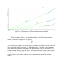
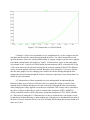
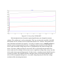
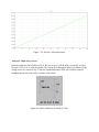
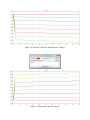
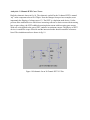
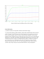
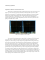
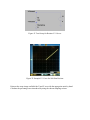
EE320L Electronics I
Laboratory
Laboratory Exercise #6
Current-Voltage Characteristics of Electronic Devices
By
Angsuman Roy
Department of Electrical and Computer Engineering
University of Nevada, Las Vegas
Objective:
The purpose of this lab is to understand current-voltage characteristics of various passive and
active electronic components and how to interpret these characteristics for the design of
electronic circuits.
Equipment Used:
Dual Output Power Supply
Oscilloscope with X-Y Capability
Breadboard
Jumper Wires
Resistors, Capacitors
Small Signal diodes (1N418 or equivalent)
NPN and PNP transistors (2N3904/2N3906 or similar)
N-Channel MOSFETs (ZVN3306A or similar)
N-Type JFET (J310 or whatever low-cost small signal JFET is available at hand)
1x Scope Probes (If available)
Background:
The first two words that come to mind when one thinks of electronics are voltage and
current. Every electrical phenomenon can be described in some form based on these two
fundamental properties. Despite this, much of electrical engineering devolves away from these
fundamentals and understanding is obscured by adding layers upon the foundation of voltage and
current. The question that needs to be asked of any electronic component is how the voltage is
related to the current. This understanding brings powerful insight into the design of electronic
circuits.
The simplest electronic component is the resistor. The resistor has a simple relationship
between voltage and current. The current flowing through a resistor is the voltage across the
resistor divided by the resistance of the resistor. The equations below show all the relationships
between voltage, current and resistance.
𝑅=
𝑉
𝑉
→𝑉 =𝐼∗𝑅 →𝐼 =
𝐼
𝑅
The value of a resistor can be determined by applying a known voltage across it and measuring
the current flowing through it. If this was to be plotted on the X-Y plane, it follows that voltage
should be on the X axis since it is the independent variable and current should be plotted on the
Y axis since it is the dependent variable. This could be reversed but generally due to the ease of
creating variable voltage sources this was the convention adopted. The plot in fig. 1 created
using LTSpice shows three resistor values and their current-voltage or I-V characteristics. It is
tempting to think of resistance as slope but in this plot the slope is really the reciprocal of
resistance, or conductance. Thus for the 0.5 ohm resistor at 10V the current is equal to
1
1
𝐼 = 𝑉 ∗ 𝑅 = 10 ∗ 0.5 = 20 𝐴. It is important to always be aware of the orientation of the axes.
Sometimes I-V plots are flipped in order to make certain data more clear. For this lab the plots
will always be shown with voltage on the X axis and current on the Y axis.
Figure 1 I-V Characteristics of 0.5Ω, 1Ω and 2Ω resistors
One may wonder what the value of plotting the I-V characteristics of resistors is, since it
is simply a straight line. In reality most resistors have some form of voltage coefficient, that is,
their value changes with the voltage applied across the resistor. This change is generally
nonlinear and can be quite complex to describe mathematically. Figure 2 shows the I-V
characteristics of the resistors with deviation from the ideal highlighted in blue. This graph is by
no means typical of resistors; its sole purpose is to show that resistors aren’t always linear
devices. Generally this consideration is reserved for niche applications such as power electronics.
In this lab the focus will be on more widespread nonlinear devices such as diodes and transistors.
Figure 2 I-V Characteristics of non-ideal 0.5Ω, 1Ω and 2Ω resistors
The semiconductor diode is a two terminal nonlinear device. The current through the
diode as a function of voltage across it is given by,
𝑉𝐷
𝐼 = 𝐼𝑆 (𝑒 𝑛𝑉𝑇 − 1)
The derivation of this equation and the meaning of its variables are outside the scope of this lab
and the interested reader is referred to the “additional resources” section. It is obvious that the
current follows an exponential relationship to the applied voltage. The I-V characteristics of a
1N4148 switching diode are shown in figure 3. The exponential shape is clearly visible, however
it straightens out around 0.9V. This is because of a series resistance that is part of the diode’s
package. A larger diode would continue to display an exponential characteristic at higher
voltages.
Figure 3 I-V Characteristic of a 1N4148 Diode
Creating I-V plots of two terminal devices is straightforward; vary the voltage across the
terminals and measure the current flowing through the device. For a three terminal device the
question becomes what to do with the third terminal. A stepped voltage or current can be applied
to the third terminal which will result in a “family” of characteristic curves on the same graph.
An example of an I-V plot for a 2N3904 bipolar junction transistor (BJT) is shown below in fig.
4. The traces shown are the currents flowing into the collector terminal of the BJT for different
values of current applied at the base terminal. Basically, many different I-V curves are laid out
onto the same graph to see how changing one variable, the current flowing through the base
changes the current flowing through the collector. Each trace represents a base current from 0 to
100uA in 25uA increments.
I-V characteristics of three terminal devices are indispensable in understanding the
behavior of these types of devices. The basic idea is to change the voltage or current at one
terminal, hold it constant and then see how the current flows through the other two terminals
while changing the voltage applied across those two terminals. This concept can be extended to
any three (or more) terminal device such as vacuum tubes, transistors, JFETs, MOSFETs,
silicon-controlled rectifiers (SCRs), thyristors, unijunction transistors (UJTs), IGBTs, HEMTs,
etc. The beauty of testing the I-V characteristics of a device is that the user can design a circuit
for that device without knowing or understanding any of the physics or fundamental operation of
the device. If a new electronic device were to be invented, the first thing the inventor would do is
make an I-V plot.
Figure 4 I-V Curves for a 2N3904 BJT
Most instruments in an electronics engineering laboratory are designed to measure
voltages. The oscilloscope is such an instrument. There are current probes available, both Hall
Effect based for DC currents as well as transformer based for AC currents. These probes have
many limitations and tend to be expensive. As such it is common to use a sampling resistor to
measure currents in many practical circuits. A sampling resistor is placed in series with the
device under test and the voltage drop across it is proportional to the current flowing in the
device. Of course, adding a resistor in series with a device will modify the operation of the
device under test. For example, if the resistor causes a significant voltage drop, it may cause the
device under test to stop working properly. For this reason, a sampling resistor should always be
as small as possible. The limitation for how small the resistor can be usually depends on the
noise of the test equipment being used; a very small voltage drop may be below the voltage
resolution of the measuring instrument.
Prelab:
Analysis 1: Resistor Curve Trace
The most basic I-V plot is that of a resistor. Draft the schematic shown below in fig. 5.
Figure 5 LTSpice Schematic for Resistor I-V Plot
Next, edit the simulation command and select the “DC sweep” tab and enter the values as shown
below in fig. 6. All other simulations in this lab will be of the DC sweep type. A DC sweep tells
LTSpice to sweep a voltage or current source from one value to another in the given increment.
The entered values tell LTSpice to sweep the source “V1” from 0 to 10V in increments of 10mV.
10mV was chosen as an increment to give a smooth looking curve. Larger or smaller increments
can be used as needed based on the situation.
Figure 6 DC Sweep
Figure 7 I-V Plot for a 100 ohm Resistor
Analysis 2: Diode Curve Trace:
Draft the schematic shown below in fig. 8. Be sure to use a 1N4148 diode. Set the DC sweep to
be from 0.4V to 1.8V in 10m increments. The current flow through the diode as a function of the
voltage across it is shown in fig. 9. Note the exponential nature of the curve and the eventual
straightening out due to the series resistance in the diode.
Figure 8 LTSpice Schematic for Diode I-V Plot
Figure 9 I-V Plot for a 1N4148 Diode
Analysis 3: NPN BJT Curve Trace:
Since a BJT is a three terminal device, the procedure for the DC sweep will change from the
previous examples. Draft the schematic shown below in fig. 10. The two resistors are not
necessary for simulation but they will provide a result that is more similar to actual lab
experiments. To get an accurate characterization of the BJT, the voltage source should be
directly connected to the base and the emitter resistor omitted.
Figure 10 LTSpice Schematic for NPN BJT I-V Plot
Edit the simulation command to match the values shown in fig. 11. Note that a second source
needs to be swept as well. The second source is the voltage applied to the base. Note that the
number of steps for the second source is the number of curves that will appear in the final plot.
One can use as many steps as desired but if the steps are too close together the plot will appear
too busy. It is better to pick a few key points. The second source is stepped from 0 to 2V in
increments of 0.2V resulting in 10 curves. Plotting the current through the collector gives the
result shown in fig. 12.
Figure 11 DC Sweep for BJT I-V Plots
Figure 12 Collector Current for Different Base Voltages
Analysis 4: PNP BJT Curve Trace:
For a PNP device, the schematic needs to be modified in order to get a result that is similar to the
NPN BJT. Draft the schematic shown below in fig. 13. The PNP is flipped so that the emitter is
the most positive terminal. The base bias voltage is referenced to the positive supply instead of
ground. The values for the DC sweep do not change from the previous example. That is the main
reason for using this configuration. There are a few alternate ways to create I-V plots for a PNP
BJT with the end result being the same after proper manipulation of the curves. Fig. 14 shows
the plot of the collector current. The plot can be flipped by right-clicking on the trace label for
“Ic(Q2)” and adding a minus sign to the expression as shown in fig. 15. This procedure (or some
other variation) needs to be done for P-type MOSFETs or JFETs as well in order to match the
polarities of N-type devices.
Figure 13 Schematic for PNP BJT I-V Plot
Figure 14 Collector Current for Different Base Voltages
Figure 15 Flipping the Collector Current
Analysis 5: N Channel MOSFET Curve Trace:
Draft the schematic shown in fig. 16. Note the changes in the DC sweep values from the
previous examples. The 100k resistor to ground is not needed for simulation but is needed in a
practical lab in order to prevent stray voltages from appearing on the gate of the MOSFET when
the voltage source is disconnected, or if, for some reason, the gate is coupled with a capacitor to
the voltage source. The 10 ohm resistor is not needed either, but the voltage drop through this
resistor will translate to current flow in our lab experiment.
Figure 16 Schematic for an NMOS I-V Plot
Figure 17 Drain Current for Different Gate Voltages
Analysis 6: N Channel JFET Curve Trace:
Draft the schematic shown in fig. 18. The schematic symbol for the N channel JFET is named
“njf” in the component selector in LTSpice. Note the changes from previous examples, most
importantly the flipping of voltage source V2. The JFET is a depletion mode device. Unlike
previous three terminal devices which have increasing collector or drain current with increasing
base or gate voltage, the JFET exhibits decreasing drain current with increasing gate current.
With zero volts applied to the gate a JFET conducts its maximum current. The physics of JFET
devices is outside the scope of this lab and the interested reader should consult the references
listed. The simulation results are shown in fig. 19.
Figure 18 Schematic for an N Channel JFET I-V Plot
Figure 19 Drain Current for Different Values of Gate Voltage
Prelab Deliverables:
1). Submit screenshots of each prelab’s schematic and simulation output.
2). You must also include an Altium schematic, Altium netlist, and PCB layout for the circuits in
prelabs 1 through 5. Each PCB layout must include footprints for all components used and can
be auto routed or manually routed. You may use either thru-hole footprints or surface mount
footprints for each component. (For the voltage and current sources just put a two pin header and
label them VCC and GND.) Also include a grounding plane and make sure your traces are wide
enough for the increase in current. To determine the trace width use a PCB trace calculator. If
you are unsure how to use Altium please click on the Lab Equipment, Learning, Tutorials,
Manuals, Downloads link on the UNLV EE Labs homepage and read the Altium tutorial or
watch the videos. https://faculty.unlv.edu/eelabs/index.html?navi=main_labequipment
Laboratory Experiments:
Experiment 1: Resistor I-V Characteristic Curves
Measure the I-V characteristics of the 100 ohm resistor in fig 5. First set the scope to X-Y
mode. If you are unsure how to do this consult the user manual for the scope since it will be
different for every scope. In X-Y mode there is no time axis. Both axes are in terms of voltage.
Apply a known voltage to both channels and verify which channel represents which axis.
Generally channel one is X and channel two is Y. Fig. 20 below shows what happens if 5V is
applied to the X input and the Y input independently. Note the scale factors. Spend some time
getting comfortable with X-Y mode.
Figure 20 5V applied to X and Y inputs
Next, set up the function generator to output a fairly low frequency (20-100Hz) triangle
wave. This will serve as the linear voltage sweep just like in LTSpice simulations. Set the
amplitude to a value of about 5V. If the voltage is set too high then the function generator may
not be able to drive the load. This will vary between different instruments. A schematic of the
test set-up is shown below in fig. 21. The voltage sweep is connected to the X-input and the
junction between the main resistor and the sampling resistor connects to the Y-input. It is up to
you to pick the value of the sampling resistor. Ideally the resistor should be as small as possible
since this reduces error but the noise of the scope may not make the measurement meaningful.
The reason for using 1X probes is to reduce the noise as well. You will have to adjust the scale
factors in order to see the desired slope. Otherwise the X-Y plot may look like a straight line. An
example of a resistor I-V plot on a scope is shown in fig. 22. Note the difference in scale factors.
If you understand the concepts presented in this lab, then it will be simple to figure out the value
of the sampling resistor used based on the scope picture.
Figure 21 Test-Set-up for Resistor I-V Curves
Figure 22 Example I-V Curve for 100 Ohm Resistor
Print out the scope image and label the X and Y axes with the appropriate units by hand.
Calculate the percentage error introduced by using the chosen sampling resistor.
Experiment 2: Diode I-V Characteristic Curves
Measure the I-V characteristics for the 1N4148 diode. An example test set-up is shown
below in fig. 23. The procedure is the same as for the resistor. However, keep in mind that the
diode’s voltage range of interest is fairly low around 0-1.5V. At high voltages there will be
significant current flow and it may be excessive for the function generator.
Figure 23 Test-Set-up for Diode I-V Curves
Print out the scope image and label the X and Y axes with the appropriate units by hand. Since
the diode is a non-linear device it is difficult to really define a single value of error. Instead,
comment on if you can see the straigthening out of the diode’s I-V curve and to what degree the
sampling resistor is affecting it.
Experiment 3: NPN BJT I-V Characteristic Curves
For a three terminal device such as an NPN transistor we need to hold the voltage applied
at the control terminal (base or gate) constant while sweeping the voltage applied to the collector
or drain terminal. Build the test set-up shown below in fig 24. In this set-up a DC voltage supply
is connected to the base through a 10k or similar value resistor. When the voltage applied is zero
then the I-V characteristics should just be a horizontal line. As the voltage is raised the curve
should take the shape shown in fig. 25. Repeat this for a few values of base voltage.
Figure 24 Test-Set-up for NPN BJT I-V Curves
Figure 25 Example I-V Curve for an NPN BJT at a Particular Base Voltage
Save each image and then combine onto one graph by hand. If you have a scope with high
memory depth and infinite persistence then you may be able to plot all the curves on the same
screen. Label all axes appropriately. Furthermore, label the value of the base voltage applied to
each curve in your graph.
Experiment 4: PNP BJT I-V Characteristic Curves
The test set-up needs to be changed for a PNP transistor to reflect differences in polarities
required. Build the test set-up shown in fig. 26. Follow the same procedure as the previous
experiment.
Figure 26 Test Set-up for PNP BJT I-V Curves
Experiment 5: N-Channel MOSFET I-V Characteristic Curves
Adapt the schematic shown in figure 16 to create your own test set-up. Do not omit the
resistor from the gate to ground otherwise you may get unusual results based on stored charges
on a floating gate. Create a family of curves as in the BJT examples.
Experiment 6: N-Type JFET I-V Characteristic Curves
Adapt the schematic shown in figure 18 to create your own test set-up. Do not omit the resistor
from the gate to ground otherwise you may get unusual results based on stored charges on a
floating gate. Create a family of curves as in the BJT examples.
Postlab Deliverables:
1. All images, graphs and percent error calculations indicated in the experiment
descriptions.
2. Questions:
a. What is the name of a dedicated instrument that creates I-V characteristics? How
does this instrument work? (Hint: there are two different types of instruments that
do this function. One of them is not in use anymore.)
b. Why did we always place our sampling resistor between our device under test and
ground? What would happen if instead the sampling resistor was placed between
the voltage source (function generator in this lab) and the device under test? How
would the I-V characteristics change? (hint: think about offset voltages and BJT
saturation)
c. If there was a situation where one had to insert a current sampling resistor in a
circuit and one side could not be grounded, what can be to get an accurate current
reading? (hint: look up differential measurements)
d. What are two other methods of measuring current in a circuit using an
oscilloscope? These methods both involve using two types of specialized probes,
one of which can only measure AC and the other can measure AC and DC.
This is a picture of diode I-V characteristics done on a scope with low noise. The sampling
resistor is 0.1 ohm. Knowing the ability of your test equipment is important.