1
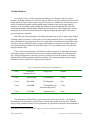
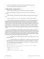
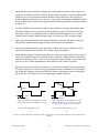
Experience of PrimeTime STA Signoff
Jason Chen
Senior CAD Engineer
Silicon Integrated Systems Corp.
No. 16, Creation Rd. I, Science-based Industrial Park
Hsin Chu, 300
Taiwan, R.O.C
[email protected]
ABSTRACT
PrimeTime is a successful and de facto static timing analysis (STA) signoff tool. We have used
PrimeTime to signoff several chips. It does have many advantages to help designers to find timing
violations both in pre-layout and post-layout stage. It also can find inconsistency between input data,
and it has capability to handle large designs and constraints. In this paper, we want to share the
experience of using PrimeTime successfully to verify timing issues of designs and hope all of you
could benefit from it. The following topics will be included: capacity and performance of PrimeTime,
design guidelines leading to PrimeTime success, tips to debug timing violations, STA issues such as
the impact of non-clocked designs and register feedback path.
1.0 Introduction
As we know STA is a really important methodology in IC design because we need to
guarantee all timing constrains are met before tape out. Until now we have used PrimeTime to verify
timing both in pre-layout and post-layout stage and it shows us a reliable tool. The facts have been
proven: it has helped designers to find potential timing violations in pre-layout stage, hand off
complete set of constraints to APR, identify the consistence between input data (RC file, SDF,
constraints and netlist), and find timing violations in post-layout phase. The designers also used its
timing reports to predict the maximum speed of chip and compare to online speed. The result of
speed comparison is matched.
PrimeTime has many advantages. It has high performance and is able to analyze large designs.
Its timing analysis is accurate. It is also able to create timing model for IP core. It is equipped with
many commands to help designers to check the completeness and consistence of input data, and to
report the coverage of timing analysis. It supports the method to emulate the real clock scheme in
pre-layout and includes clock tree in post-layout stage. It is also possible to report all paths if the
designers intend to do it.
Table 1 shows the performance of PrimeTime with four design cases. PrimeTime does quite
well in large designs. It only takes about 6 hours to complete timing analysis for a 5M gatecount
chip. The high performance is necessary because we always have several iterations to do timing
analysis before cleaning constraints and fixing violations. If an iteration of timing analysis requires
more than 10 hours, typically the designers cannot endure it.
Table 1: Performance of PrimeTime in four design cases
Cases
Gatecount /
constraints file size
Design entry
Runtime1
Case1
250K/300KB
RTL/Synthesis
15mins
Case2
5M/14MB
RTL/Synthesis
6hrs
Case3
2.7M/2MB
RTL/Synthesis and
Schematic entry mixed
Case4
1.8M/3MB
Schematic entry
3.5hrs
10hrs
The performance of PrimeTime is not always good for each case in Table 1. We found an
interesting fact: the performance of PrimeTime is related to the method of design entry. When the
design is fully synthesized from RTL, the performance is proportional to the gatecount and amount of
1
Full chip STA, and the runtime includes to report all violations with full path information.
SNUG Taiwan 2001
2
Experience of PrimeTime STA Signoff
the constraints. We can see this trend in case1 and case2. When design entry is mixed with
RTL/synthesis and schematic entry, or fully schematic entry, the examples are case3 and case4, the
performance turns worse.
Until now we still don’t know the reason causes performance of PrimeTime worse. What we
only know is, when the design is created from RTL/synthesis flow, this kind of designs is very
suitable for STA.
1.1 STA Policies in SiS
The STA policies what we discuss here are the general STA rules and we had better to
follow2. The STA policies includes:
1. Central delay calculator: we like to use only one delay calculator to create SDF
from RC files. All verification tools include simulation and STA then use the same delay. Doing
this to avoid inconsistency delay from multiple delay calculators.
2. Full chip STA: it is easier to build up STA for full chip than to build up for each subblock. And sub-block timing analysis usually results in inaccuracy of boundary timing
constraints.
3. Use On-Chip-Variation analysis mode in PT: in on-chip-variation mode, PT will
analyze timing by using max delay in data path and min delay in clock path to check setup time,
min delay in data path and max delay in clock path to check hold time. In this way we get more
accurate analysis result.
1.2 SiS STA Flow
The STA flow shown in Figure 1 is quite formal. We extract parasitics (RC) and use a delay
calculator to calculate parasitics into two SDF file, both worst and best case, and then back
annotate these SDF files into PT to check setup and hold time issues respectively.
2
Depending on your requirement, you may have different STA policy.
SNUG Taiwan 2001
3
Experience of PrimeTime STA Signoff
dspf (RC)
worst and best
Synopsys library
delay calculator
worst and best
SDF
constraint
verilog
PrimeTime
reports
Figure 1. PrimeTime STA Flow
2.0 Design Guidelines leading to STA success
To get the success of STA, from our experience, there are five essential guidelines we need to
follow. They are synchronous design, design by RTL to synthesis flow, full-constrained design,
reliable RC model and timing library, reports to perform complete analysis. Below I give brief
comments on each guideline:
1. Synchronous design: STA is suitable for synchronous design. We strongly
recommend our designers to follow this unquestionable motto.
2. Design by RTL to synthesis flow: we have revealed this claim by showing the
performance of five designs in Table 1. More than one thing needs to be mentioned, use the
designs use RTL to synthesis flow could smoothly transfer all design data to PT because both
synthesis and PT load the same data: netlist and timing constraints. To create constraints and
well verify in synthesis phase, almost we don’t need change anything before starting PT.
3. Full-constrained design: the judgement of this condition is quite easy! PT can’t
analyze the designs without constraints and its timing result will be non-predicable.
4. Reliable RC model and timing library: the accuracy of all timing reports of PT is
based on the degree of timing value. The incorrect RC model and timing library will get invalid
timing report, even we are very careful and work hard on each steps of STA!
5. Reports to perform complete analysis: we need the verification tool has one ultimate
ability ─ if tool reports no problem, then the design should be no problem and could be tape
out Cheer! Currently PT provides full set of reports to achieve this ability. By carefully
SNUG Taiwan 2001
4
Experience of PrimeTime STA Signoff
checking reports, the designers could feel confidence that their STA works are no
questionable. I will elaborate this guideline in next section.
3.0 High quality of timing analysis
We have a question when we use PT or similar STA tool to analyze our designs:
How could we make sure all design has been analyzed and all input data are no
problem?
In this section I hope I could answer this question. This question could be issued in the other
way:
Which kind of reports we need to check to guarantee no timing problem in design?
Usually the designers want to know how good his timing analysis is. He want a high quality of
analysis to make sure chips will work after tape out. What is the exactly definition of quality for
timing analysis? Here is my definition: the version of input files is correct, input files are consistent
between each other, completely link your design to correct library (no black box exist), delay is fully
backannotated, fully constrain design, how many abnormal in design that let PT hard to do timing
analysis, and the most important, how many constraint in your design and how many are violated
(analysis coverage). I believe each designer who uses PT should have the similar checklist to explore
reports.
It is easy to check the quality of timing analysis because PT has provided log/reports for us. I
will elaborate these helpful log and reports, and show possible mistakes you might encounter. Before
doing that I need make a clarification: PT can’t tell you the version of input files is correct or not, you
must check by yourself. But from the report or log you could get a chance to check the version of
input files. The sequence of log and reports are discussed below almost coincides with the sequence
of execution in PT user flow, from reading design to reporting timing.
1. Read netlist (read_verilog): the frequency mistakes are missed file, incorrect version,
and syntax error.
2. Link design (link_design): To check if there is any unresolved reference (unexpected
black box), and it is successful or not to link design, correct version of libraries are loaded or
not. You must make sure no unexpected black box after linking, or the paths related to black
box are not analyzed. Here is a sly example.
Linking design TOP...
Warning: Unable to resolve reference to 'BUFX1' in 'TOP'. (LNK-005)
Creating black box for B1/BUFX1...
Designs used to link TOP:
<None>
Libraries used to link TOP:
ptlib
Design 'TOP' was successfully linked.
1
SNUG Taiwan 2001
5
Experience of PrimeTime STA Signoff
3.
Back annotation (‘read_sdf’, in conjunction with reports of
‘report_annotated_delay’ and ‘report_annotated_delay’): to make sure SDF files are no
problem and all delay arcs are annotated. These log and reports could tell you the answer. The
log file of read_sdf shows the errors when delay can’t be back annotated to design. Below are
some occasional errors.
Error: Cannot find instance 'L1'. All delays related to that instance
are ignored. (SDF-011)
Error: No net timing arc from pin 'RI7/Z' to pin 'U345/A'. (PTE-014)
Error: Net delay from pin 'UCLKBUF/U1725/Z' to pin 'UA/GRSTN_C1/A'
cannot be annotated because of a timing assertion on hierarchical pin
'UCLKBUF/GRSTN'. (PTE-015)
Usually the first two errors are occurred from the fact that the netlist and SDF are inconsistent.
Check your netlist and SDF version and recover this kind of errors. The third error is due to the
path being disabled by command ‘set_disable_timing’, and this forbid PT to annotate SDF net
delay. This is not a symptom of inconsistency and we can avoid it by changing the sequence of
‘read_sdf’ and ‘set_disable_timing’, i.e. read SDF before disable timing.
The commands ‘report_annoated_delay’ and ‘report_annotated_check’ with option –
list_not_annotated could show messages to tell us that the expected delays are not annotated.
Below is an example of ‘report_annotated_delay –list_not_annotated’.
Non backannotated cell delays:
-----------------------------1. U2/A -> U2/Z (sense: positive_unate)
Non backannotated internal NET delays:
-------------------------------------1. U2/Z -> DL2/D
|
|
|
NOT
|
Delay type
|
Total | Annotated | Annotated |
-----------------------------+-----------+-----------+-----------+
cell arcs
|
6 |
5 |
1 |
internal net arcs
|
6 |
5 |
1 |
net arcs from primary inputs |
2 |
2 |
0 |
net arcs to primary outputs |
1 |
1 |
0 |
-----------------------------+-----------+-----------+-----------+
|
15 |
13 |
2 |
Again, this kind of warnings also warns us the possible inconsistent between netlist and SDF.
Another possible reason is something wrong in the SDF file. If some nets are broken in APR,
the delay calculator can’t, of course, calculates parasitics to delay. Figure 2 shows this case.
Check your APR database to find this possible issue and recover it. Or, the final possible
reason is, the buggy delay calculator creates incorrect SDF.
SNUG Taiwan 2001
6
Experience of PrimeTime STA Signoff
U1
U2
U3
broken
U4
*|DSPF 1.0
*
*|DIVIDER /
*|DELIMITER :
*|
*|NET NET3 6.682e+00ff
*|I (U1:Z N1I296 Z I 0.0)
*|I (U2:A N1I296 A O 0.0)
*|I (U3:A N1I459 A I 0.0)
*|I (U4:A N1I459 A I 0.0)
CG53 U1:Z 0 2.571e+00ff
CG54 U2:A 0 1.213e+00ff
CG55 U3:A 0 1.343e+00ff
CG56 U4:A 0 1.274e+00ff
CG57 NET3:110 0 1.466e-01ff
CG58 NET3:111 0 1.324e-01ff
R45 U1:A NET3:110 2.722e+01
R46 NET3:110 U2:A 1.070e+01
R47 NET3:110 NET3:111 1.070e+01
Figure 2. A broken dspf net and its network
4. Apply constraints (source constraint files): the errors might be occurred when you
source constraints and we need to check and recover it. The possible errors are case
mismatch, invalid object in ‘–from/-to’, can’t find object in netlist, and assert hierarchical pin as
port. The command ‘current_design’ is frequently misused in PT script because it has different
behavior in DC and PT3. In DC we usually use this command to set to desired sub-design
when we include constraints. However, in PT we can only use one time to set top design
before linking the design. Using ‘current_design’ command to change current design will force
PT remove all constraint from design and re-link it again. Although this is not a true error, but a
frequent misuse even by a DC expert. You should be aware that PT doesn’t tell you the
exception is ignored when you apply constraints into design. You need to use the command
‘report_exception –ignored’ to get this message.
5. Check timing (‘check_timing’): this command is very powerful and we should be
very careful to check the report. It shows all abnormal design in netlist, abnormal constraint
and all unconstrained point for you. Abnormal cases are multiple clocks fan into register’s
clock pin, latch fanout, loops, no clock, ignored exceptions, w/o maximum constraints, input
port w/o input delay, and the invalid generated clock. In order to fully constrain deign, it
become essential to check the report of ‘check_timing’.
There is a warning message may always confuses PT user. That is ‘large common period
warning’. We only are warned that the performance of PT will be affected heavily by this
warning but don’t know why and where and then don’t know how to fix it. The command
‘check_timing’ should be improved to tell user the reason. Currently the only strategy to
prevent it is to define false path to all unrelated clocks4.
3
The article SYNTH-482056.html in SolvNET also gives a clarification about misuse of current_design in PT.
SolvNET article Static_Timing-199.html gives another tip to avoid clock period expansion, which is to define all
input port delay.
4
SNUG Taiwan 2001
7
Experience of PrimeTime STA Signoff
Report clock information (‘report_clock’): maybe not all clocks are created in
command ‘create_clock’. We can check it in log of create_clock, and also in report of
command report_clock. We also need to make sure the waveform and period of clocks are
correct or not. An example that clock can’t be created is clock source doesn’t existed in netlist.
This is occurred that the definition point of clock created in pre-layout netlist is disappeared in
post-layout netlist. Figure 3 shows this case.
6.
Post-layout Netlist
Pre-layout Netlist
D
D
Q
D
Q
D
C3
Q
PLL
PLL
C1
Q
CLK1_BUF_1 CLK1_BUF_2
Q
C2
Q
CLK2_BUF_1 CLK2_BUF_2
Q
create_clock -name {CLK1} -period 10
-waveform [list 0.0 5.00] [get_pins
{C2/Z}]
create_clock -name {CLK2} -period 10
-waveform [list 0.0 5.00] [get_pins
{C3/Z}]
Q
create_clock -name {CLK1} -period
10 -waveform [list 0.0 5.00] [get_pins
{CLK1_BUF_1/Z}]
create_clock -name {CLK2} -period
10 -waveform [list 0.0 5.00] [get_pins
{CLK2_BUF_1/Z}]
Figure 3. Clock source disappear in port-layout netlist
7. Report analysis coverage (‘report_analysis_coverage’): when we need to answer
the question of how many violations in STA, we do check this report. This report directly
shows you the quality of timing analysis in number. It tells you how many constraints in design,
how many of them are met or violated. Further, it can show you which constrain is not
analyzed due to a specific reason by adding an option -status_details {untested}. The
command ‘check_timing’ also could tell you the similar untested information but without
reason.
SNUG Taiwan 2001
8
Experience of PrimeTime STA Signoff
Report exception information (‘report_exception’): if we want to display the ignored
exceptions, we use command ‘report_exception –ignored’. The same information is also shown
in the report of command ‘check_timing’. However, both of these two commands don’t show
the ignored reasons. The possible reasons cause exceptions ignored are incorrect object,
unconstrained path, and unchanged constraint.
Another reason that may cause exceptions to be ignored is the exception precedence rule. This
usually confuses the designers. Figure 4 shows an example of exception precedence rule. In this
example, even we set three cycle path after mcp 2, PT does apply mcp 2.
Apply incorrect exception is the fault of designers, but if PT can give warning message for the
exception precedence rule, it would be better. However, the command ‘report_exception’ as
well as ‘check_timing’ don’t report this information.
8.
D
Q
Q
D
U2
Q
U3
Q
U1
U4
according to exception
precedence rule, mcp = 2
script to set mcp for path U1/CK to U4/D:
set_multicycle_path 2 -setup -through [get_pins {U3/Z}]
set_multicycle_path 3 -setup -through [get_pins {U2/B}]
Figure 4. An example shows exception precedence rule
9. Reports timing and constraints (‘report_constraint’ and ‘report_timing’): finally,
when we wander how the paths are violated, we can use these two commands. At first you
must check whether the right options are used. The frequent misuse is missing ‘–delay_type
min’ when you want to check hold time issue. Second, when you analyze post-layout STA,
you must check all clocks and generated clocks are set to be propagated, i.e., include the
delay of clock tree in timing analysis. Use ‘set_propagated_clock [all_clocks]’ to turn ideal
clocks to propagated clocks.
4.0 Tips to debug and fix timing violations
When we complete report_timing and find violations in report, the next jobs is to debug and fix
violations. Designers need equip themselves with some prerequisite knowledge to help them find the
reason of violation. In this section the possible reasons that cause timing violations are shown.
1.
Large loading and large transition cause setup time violation: both of these two factors are large
result in large delay and causes setup time violation. To fix it, common strategies are decrease
loading by inserting buffer, size cell, or re-optimize design.
SNUG Taiwan 2001
9
Experience of PrimeTime STA Signoff
2.
Small path delay causes hold time violation: this usually happens in back-to-back register, for
example, scan path from FF1/Q to FF2/SI. Another kind of example is register feedback path,
which also easy to have hold time violation. But this is false path because our registers are
usually designed as hold time free for this case. Check with circuit designer or datasheet. If this
is true, set false path to all this kind of paths. Register feedback path will be discussed in details
in section 5.3.
3.
Long net in P&R cause setup time violation: in deep submicron net delay will dominate path
delay if the length of net is too long, or net goes through too many via. This kind of net may
have delay exceed 2 ns. If routing tool can’t control of maximum length of net, it is a quite
common cause of timing violation in today design. The only way to fix it is change routing.
4.
Large clock skew and transition cause setup and hold time violation: add option –path_type
full_clock in command report_timing to check with clock skew and transition.
5.
Large delay/constraint in library cause setup time violation: when you see this kind of cause,
check your timing and spec of library cell. Confirm with circuit designer.
6.
Multi-frequency paths: PT will find critical slack in all edges of common period of two clocks if
clocks are in different frequency. Usually this causes setup time violation (another side effect is
make PT performance worse). To fix it, set it as multicycle path if possible, or set as false path
if we don’t care it. Utilize synchronizer for data transfer between clocks if possible.
7.
Phase lag clocks cause setup time violation: Figure 5 shows the example of phase lag and how
PT checks setup time. We need to study why designer creates a destination clock with phase
lag. If possible, change to in phase and add clock latency to destination clock to model phase
lag. In this way, PT will use one cycle as path budget to check setup time.
Setup
Setup
Phase
Lag
Clock
Latency
create_clock -period 10 -waveform {0 5} CK1
create_clock -period 10 -waveform {0 5} CK2
set_clock_latency 1 [get_clocks {CLK2}]
create_clock -period 10 -waveform {0 5} CK1
create_clock -period 10 -waveform {1 6} CK1
==> PT checks setup time at 1 ns.
==> PT checks setup time at 5+1=6 ns.
(a)
(b)
Figure 5. (a) Setup check in a phase lag clocks, which is easy to cause setup violation. (b) use clock latency
instead.
SNUG Taiwan 2001
10
Experience of PrimeTime STA Signoff
8.
Bidirection paths cause false violation: normally we don’t need to verify timing of bidirection
path because it is a functional false path. See Figure 6. If cell lead to bidirection port is defined
as tristate, we could set variable “timing_disable_bidirection_path” to true to force PT don’t
analyze these paths. One condition escapes from this variable, that is, when cell leading to
bidirection path is not defined as tristate. The only one method to fix it is to set false path on this
path.
It is a trouble if these kind of false paths are numerous. Use Tcl to set false path in one
command might be possible if these cells and the paths are the same. Below is a Tcl command:
set_false_path -through [get_pins -of_objects \
[get_cells * -hierarchical -filter "ref_name == GTLOBPA0"]
-filter "lib_pin_name == Z”] \
-through [get_pins -of_objects [get_cells * -hierarchical\
-filter "ref_name == MUX21X1"] -filter "lib_pin_name == A”]
Tristate
Buffer
Bidirection
Port
Ordinary
Buffer
(a)
Bidirection
Port
(b)
Figure 6. Path to and from Bidirection port (a) derives false path from tristate buffer (b) PT can’t derive false path
from ordinary buffer and false violation might be reported
9.
Inverse clock shortens budget of path delay and cause setup time violation: this case is occurred
when the source and destination of clocks are inverse. Figure 7shows one example of this kind
of netlist and its setup check waveform. Usually we can’t change design to avoid inverse clock
so that the possible strategy is to decrease path delay.
SNUG Taiwan 2001
11
Experience of PrimeTime STA Signoff
D
Q
D
Q
Q
Q
U1
U2
CLK
U1/CK = CLK
Se
tup
U2/CK = CLK'
Figure 7. Inverse clock in destination clock path and the waveform to show setup check
10. Input ports w/o input delay and variable “timing_input_port_default_clock = true” easy to cause
hold time violation: because of without input delay, delay of path from input port usually is quite
small and cause hold time violation. This should be false violation because input delay is
impossible to be zero. To fix it, set input delay to input port, or set variable
“timing_input_port_default_clock” to false to force PT to leave input port path unconstrained.
5.0 STA Issuses with PrimeTime
5.1 Impact of non-clocked register
The term of non-clocked register is talk about a register, its clock pin has no clock source, but
controlled by other signals. A STA tool need clock for all registers, it is true in PrimeTime. A simple
example is shown in Figure 8.
IN
D
D
Q
Q
CLK
D
Q
Q
Q
U2
CLK
Q
U3
U1
Figure 8. A non-clocked register U2.
SNUG Taiwan 2001
12
Experience of PrimeTime STA Signoff
The register U2 has no clock. For this abnormal PrimeTime shows a warning in the report of
check_timing:
Warning: There is 1 register clock pin with no clock.
Clock Pin
-----------------------------------------------------------U2/CK
We must create clock for non-clocked register, or PrimeTime doesn’t analyze related paths.
Command report_analysis_coverage -status_details {untested } shows these untested paths:
Constrained Related
Check
Pin
Pin
Type
Slack Reason
-------------------------------------------------------------U2/D
CK(rise) setup
untested no_endpoint_clock
U2/D
CK(rise) hold
untested no_endpoint_clock
U3/D
CK(rise) setup
untested no_startpoint_clock
U3/D
CK(rise) hold
untested no_startpoint_clock
The timing reports to U2/D and to U3/D are
Startpoint: IN (input port clocked by CLK)
Endpoint: U2 (rising edge-triggered flip-flop)
Path Group: (none)
Path Type: max
Point
Incr
Path
-------------------------------------------------------------input external delay
1.00
1.00 r
IN (in)
0.00
1.00 r
U2/D (FD1X1)
0.00
1.00 r
data arrival time
1.00
-------------------------------------------------------------(Path is unconstrained)
Startpoint: U2 (rising edge-triggered flip-flop)
Endpoint: U3 (rising edge-triggered flip-flop clocked by CLK)
Path Group: (none)
Path Type: max
Point
Incr
Path
-------------------------------------------------------------U2/CK (FD1X1)
0.00
0.00 r
U2/Q (FD1X1)
0.41
0.41 r
U3/D (FD1X1)
0.00
0.41 r
data arrival time
0.41
-------------------------------------------------------------(Path is unconstrained)
To constrain U2 and related paths, use command create_generated_clock to create a clock on
pin U1/Q:
create_generated_clock -divide_by 1 -source CLK [get_pins U1/Q]
SNUG Taiwan 2001
13
Experience of PrimeTime STA Signoff
DATA1
READY1
D
Q
G
Q
D
CLK
DATAn
READYn
D
Q
G
Q
Q
D
Q
Q
D
Q
Q
D
Q
Q
(b)
(a)
generated_clock
D
D
D
Q
Q
Q
Q
G
Q
U2_n
D
Q
Q
G
Q
U2
Q
D
U3
Q
D
D
Q
U1
Q
D
CLK_div16
Q
U4
Q
Q
U5
Q
Q
(C)
(d)
Figure 9. Four tricky non-clocked designs (a) use latches to latch input data, trig signal is also from outside, (b)
ripple counter, (c) composite clock source, (d) generated clock at the start of path to U5/D.
Not all the cases of non-clocked registers are easy to deal. In Figure 9(a), a considerable
number of registers are used to latch input data from the outside. Note that all signals connecting to
clock pins are not clocks. Even we want to create clocks for them, it is hard to give period and
waveform. Furthermore, we need creates clocks for each one. In Figure 9(b), a ripple counter is
used to generate clock with long period. It need to create N clocks if there are N registers in a
counter. In Figure 9(c), there are multiple source to compose the clock of U2/CK. How to create
clock for it? The last case in Figure 9(d) is interesting. We need a generated clock on U1/Q for latch
U2/G, … , and U2_n/G, which is no problem. But PT gives the following timing report for the path
to U5/D:
Startpoint: U1/Q (clock source 'U1/Q')
Endpoint: U5 (rising edge-triggered flip-flop clocked by CLK)
Path Group: CLK
Path Type: max
Point
Incr
Path
--------------------------------------------------------------clock U1/Q (fall edge)
2.50
2.50
clock source latency
0.46
2.96
U1/Q (FD1X1)
0.00
2.96 f
U3/Z (AN2X1)
0.78
3.74 f
U4/Z (OR2X1)
1.45
5.19 f
U5/D (FD1X1)
0.00
5.19 f
data arrival time
5.19
clock CLK (rise edge)
SNUG Taiwan 2001
5.00
14
5.00
Experience of PrimeTime STA Signoff
clock network delay (ideal)
0.00
5.00
U5/CK (FD1X1)
5.00 r
library setup time
-0.27
4.73
data required time
4.73
--------------------------------------------------------------data required time
4.73
data arrival time
-5.19
--------------------------------------------------------------slack (VIOLATED)
-0.46
See, the startpoint is generated clock! And is fall edge! We only have half of one cycle in this
path and eventually setup violation is reported. Oops! Maybe it is not so surprised when we
understand generated clock overrides original signal. Generated clock has two transitions, rise at 0ns
and fall at 2.5ns. PT just follows the rule of timing check to select critical condition. In fact, there is a
simple solution for this problem: move generated clock from U1/Q to U2/G… U2_n/G. This time all
latches have clocks and report of U5/D is correct. But create so many generated clocks for them
become a trouble.
Consequently, we face a dilemma: to get correct report of U5/D, create N generated clocks
on the G pin of these latches. But it is a trouble. Or, create generated clock on U1/Q but get wrong
report of U5/D. What is your decision?
Non-clocked design truly reduces the analysis coverage and hard to recover it by only using
command create_generated_clock. All designers should be aware of this fact and own the duty to
avoid this design style.
5.2 Register self-feedback path
Figure 10 shows the examples of register self-feedback path. What is the problem within this
netlist? This kind of feedback path is easy to hold time violation in PT because path delay is smaller
than hold time of D pin. But circuit designer guarantee this kind of paths is hold time free. Therefore,
all hold violations of this kind of paths are false violation and we need a solution to avoid this
problem.
Z
U2
A
A
D
Q
D
Z
Q
D
Q
U2
Q
U1
(a)
Q
Q
U1
(b)
U1
(c)
Figure 10. (a) Directly feedback. (b) Feedback through a buffer. (c) Feedback through multiple gates.
SNUG Taiwan 2001
15
Experience of PrimeTime STA Signoff
In PT a variable timing_self_loops_no_skew is related to this problem. When it is set to false,
clock uncertainty is not eliminated from timing analysis. And set to true to eliminate clock
uncertainty. What we should be aware is that no matter this variable is set to true or false, it is still
hold time violation in register feedback path. The reason is the same. So we can’t use this variable to
solve problem.
Another available solution is use option ‘-ignore_register_feedback feedback_slack_cutoff’ in
command report_timing. We all think this should be the final answer of the register feedback path
problem, but we are wrong. After testing a simple netlist, in which there are some registers of
FD1X1, FD1SX1 and FD2QX1, we found that this option only works when register type is
FD1X1. That is, PT reports “No Paths” when register is FD1X1, and reports hold time violation
when the register is other type than FD1X1, like FD1SX1, no matter what value we set to
feedback_slack_cutoff. So, this is not the correct solution.
When we recognized the only method is to set false path, a Tcl script is created to achieve this
job:
foreach_in_collection reg [all_registers] {
set reg_name [get_attribute $reg full_name]
set_false_path -hold -from $reg_name -to $reg_name
}
The result of this Tcl script was met our expectation when we check pre-layout STA. But an
amazed result was encountered in post-layout STA: out of memory. When w realized it needs huge
memory to set false path to all register, no matter whether there is feedback path in a register, we
were not surprised no longer and tried to find another solution which have the same effect and also
save memory usage5. Fortunately, the solution does exist. Command set_disable_timing has the
same effect as command set_false_path, and it also saves memory. The command for the example in
Figure 10(a) is
# for case (a)
set_disable_timing – from CK – to D [get_cells {U1}]
# for case (b) & (c)
set_disable_timing – from A – to Z [get_cells {U2}]
For real case, we wrote a program to find all register feedback path and use
set_disable_timing to break them. In this way PT could both get rid of this kind of false violation and
save memory usage.
5.3 Signal Integrity problem
Today in deep submicron, the problem of signal integrity becomes more and more important. It
is touchy problem because until now we still don’t have an effective tool could help designers to
prevent it in APR, and detect it in timing verification. It is very bad to let the designer see signals
interfered by cross talk in oscilloscope.
5
Similar topic is discussed in SolvNET article “Static_Timing-56.html”
SNUG Taiwan 2001
16
Experience of PrimeTime STA Signoff
Good news is that Synopsys has announced PrimeTime-SI at April 2001. How to integrate it
into STA flow is the next mission in SiS.
6.0 Conclusion
PrimeTime does the good job on STA. it equips full set of reports to show how good of quality
in timing analysis. These reports help designer find and fix problems, and get high confidence in his
timing analysis. But still there are three problems stand in front of us:
1. Performance is worse in some chip. We don’t know why. The only one effective
strategy to avoid it is fully synthesizing design.
2. Non-clocked register design style is hard to do timing analysis in PrimeTime. We
have presented some examples to show the difficulty. We hope the performance of PrimeTime
could be not affected by this kind of design style. On the other hand we will continue train
designer not to use this design style.
3.
SI problem currently can’t be reflected on timing analysis. We expect PrimeTime-SI
could provide a solution for this problem.
7.0 References
1.
2.
3.
4.
PrimeTime 2000.11 User Manual
Synopsys SolvNET
Desmond A. Kirkpatrick, “The Deep Sub-micron Signal Integrity Challenge”, ISPD’99.
Synopsys, “Static Crosstalk Analysis”,
http://www.synopsys.com/products/primetime_si/ptsi_techbgr.html.
SNUG Taiwan 2001
17
Experience of PrimeTime STA Signoff