1
Page 215
nanometres and this can give a pattern generator resolution grid size with many
decimal places. In addition, if the grating is defined using the ctxt facility in
CATS, “resolve” may need to be set appropriately.
19.1.14.2.
Example 2
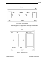
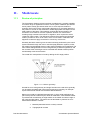
The second example pattern is an array of gates that has been designed on a
grid of 5 nm. The gate width is 100 nm and is the minimum dimension of the
pattern. The beam energy is to be 50 kV.
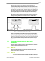
The pattern generator resolution should be set to 5 nm and the pattern generator
grid snapping mode should be set to “float” to ensure that the gate placement
accuracy is maximised. By choosing a value of B of 5 (equation 19.17) an
exposure grid of 20 nm is the result (VRU of 4) and the minimum dimension is an
integer multiple of this so an exposed gate width of exactly 100 nm can be
carried out.
Actually, more process latitude can be obtained using the technique described in
Section “Negative biasing”. All the features should have a total bias of -20 nm
applied and through an increase in the exposure dose, gate widths of 100 nm
can be obtained.
Alternatively, if less beam-on time is required and the clock frequency is at the
maximum 25 MHz, a larger beamstep will need to be used. The next available
VRU value is 8 giving a beamstep size of 40 nm, which is not a sub-multiple of
the 100 nm linewidth. One solution is to set the pattern generator grid-snapping
mode to “split_and_bury” in order to maintain the defined 100 nm linewidths.
Another solution is to apply the negative bias of –20 nm giving a defined width of
80 nm, which is a sub-multiple of the beamstep size.
19.1.14.3.
Example 3
The third example pattern is a 4 Gbit memory device. The design grid is 1 nm.
The minimum dimension is 180 nm. The beam energy is to be 50 kV.
If a pattern generator resolution grid of 1 nm is chosen to avoid grid snapping
then the maximum fieldsize for a 16-bit pattern generator will be only 65.536 µm.
This would mean a relatively large number of stage moves and an impractically
large job time. Therefore it is usual to set the pattern generator resolution grid to
be larger and accept some grid snapping. By inspection of the pattern (using for
example the “ongrid” command in the CATS converter) a grid can be found in the
range 5 to 12.5 nm for which the amount of grid snapping will be relatively small.
This may well be some integer such as 5 or 10 nm. In this example 5 nm will be
assumed to be optimal. The minimum dimension of 180 nm with B = 4 (Equation
19.14) implies an exposure grid of 45 nm. If the technique of negative biasing is
applied then biasing the pattern by -20 nm gives a minimum dimension of
160 nm and using a VRU of 8 means that the exposure grid size is 40 nm. The
minimum dimension is an exact multiple of the beamstep size which results in
these features being the correct size. Other larger features may be not be an
exact multiple of the beamstep size so either the pattern generator grid-snapping
mode should be set to “split_and_bury” or the beamstep parameter should be
defined at conversion time.
19.2.
Drift removal using ontime
The mechanical and electrical components of the VB are affected by changing
temperature and even 1°C change can have a large effect. This affects the
pattern placement accuracy for exposures that require several hours. The ontime
function can be used to remove the effects of this drift at regular intervals.
Part Number:878275
Vectorbeam Operator Manual