1
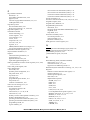
processing, 4-8
SRU (system register unit)
execution latencies, 6-40
execution timing, 6-31
overview, 1-12
Stage, definition, 6-3
Stall, definition, 6-3
Static branch prediction, 6-10, 6-26
stwcx., 4-13
Superscalar, definition, 6-3
Switching process, 4-13
sync, 4-13
Synchronization
context/execution synchronization, 2-45
control registers requirements, 2-46
execution of rfi, 4-13
memory synchronization instructions, 2-68, 2-69, A-55
SYSCLK (system clock) signal, 8-46
System
call exception, 4-23
linkage instructions, 2-65, 2-74
management interrupt, 4-26
reset exception, 4-15
System interface, see Bus interface unit (BIU)
System linkage instructions, A-56
System management interrupt, 10-2
System quiesce control signals (QACK/QREQ), 9-56
T
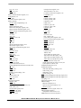
TA (transfer acknowledge) signal, 8-20, 8-36
Table search flow (primary and secondary), 5-33
TAU (thermal assist unit), 1-39, 10-6
TBEN (time base enable) signal, 2-69
TBEN (timebase enable) signal, 8-44
TBST (transfer burst) signal, 8-12, 8-28, 9-24
TCK (JTAG test clock) signal, 8-48
TCn (transfer code) signal, 8-21
TDI (JTAG test data input) signal, 8-48
TDO (JTAG test data output) signal, 8-48
TEA (transfer error acknowledge) signal, 8-20, 8-36, 9-27
Termination, address transfer, 9-20
Thermal assist unit (TAU), 1-39, 10-6
Thermal management
interrupt exception, 4-28
overview, 1-39
registers, 2-26
THRMn (thermal management) registers, 10-7
Throughput, definition, 6-3
Timing considerations, 6-9
Timing diagrams, interface
address transfer signals, 9-14
burst transfers with data delays, 9-34
L2 cache SRAM timing, 3-66
single-beat reads, 9-30
single-beat reads with data delays, 9-32
single-beat writes, 9-31
single-beat writes with data delays, 9-33
using DBWO, 9-28
using TEA, 9-35
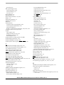
Timing, instruction
BPU execution timing, 6-22
branch timing example, 6-28
cache hit, 6-13
cache miss, 6-16
execution unit, 6-22
FPU execution timing, 6-29
instruction dispatch, 6-20
instruction flow, 6-9
instruction scheduling guidelines, 6-37
IU execution timing, 6-29
latency summary, 6-39
load/store unit execution timing, 6-30
overview, 6-3
SRU execution timing, 6-31
stage, definition, 6-3
TLB
description, 5-23
effect of a TLB miss, 6-36
invalidate (tlbie instruction), 5-25, 5-36
invalidate, description, 5-3, 5-25
LRU replacement, 5-24
management instructions, 2-78, A-58
organization for ITLB and DTLB, 5-23
TLB management instructions, 3-8
TLB miss and table search operation, 5-24, 5-31
TMS (JTAG test mode select) signal, 8-48
Trace exception, 4-23
Transient caches, 7-4
Transient instructions, 7-4
Trap instructions, 2-65
TRST (JTAG test reset) signal, 8-48
TS (transfer start) signal, 8-11, 8-27
TSIZn (transfer size) signals, 8-12, 8-28, 9-17, 9-41
TTn (transfer type) signals, 8-11, 8-27, 9-15, 9-41
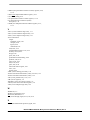
U
UBAMR (user breakpoint address mask register), 2-35
UISA (user instruction set architecture)
overview, 1-21
registers, 2-8
UISA instructions, 2-50
UMMCRn (user monitor mode control registers), 2-32–2-34,
11-8–11-10
MPC7410/MPC7400 RISC Microprocessor Reference Manual, Rev. 2
Freescale Semiconductor
Index-13