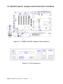
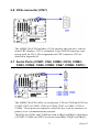
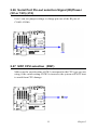
1
AIMB-740-6CB1
Socket 478
Intel® Pentium® 4/
Celeron-D
Industrial ATX Motherboard
with 6 Serial Ports
User’s Manual
Copyright Notice
This document is copyrighted, 2006, by Advantech Co., Ltd. All rights
are reserved. Advantech Co., Ltd. reserves the right to make improvements to the products described in this manual at any time without notice.
No part of this manual may be reproduced, copied, translated or transmitted in any form or by any means without the prior written permission of
Advantech Co., Ltd. Information provided in this manual is intended to
be accurate and reliable. However, Advantech Co., Ltd. assumes no
responsibility for its use, nor for any infringements upon the rights of
third parties which may result from its use.
Acknowledgements
• AWARD is a trademark of Phoenix Technologies Ltd.
• IBM and PC are trademarks of International Business Machines Corporation.
• Intel®, Pentium® 4, and Celeron® are trademarks of Intel Corporation.
• WinBond is a trademark of Winbond Corporation.
All other product names or trademarks are the properties of their respective owners.
AIMB-740-6CB1 User’s Manual
Part No. 2002C74000
1st. Edition
Printed in Taiwan
February 2006
ii
1.0.1 A Message to the Customer
Advantech customer services
Each and every Advantech product is built to the most exacting specifications to ensure reliable performance in the harsh and demanding conditions typical of industrial environments. Whether your new Advantech
equipment is destined for the laboratory or the factory floor, you can be
assured that your product will provide the reliability and ease of operation
for which the name Advantech has come to be known.
Your satisfaction is our primary concern. Here is a guide to Advantech’s
customer services. To ensure you get the full benefit of our services,
please follow the instructions below carefully.
Technical support
We want you to get the maximum performance from your products. So if
you run into technical difficulties, we are here to help. For the most frequently asked questions, you can easily find answers in your product documentation. These answers are normally a lot more detailed than the ones
we can give over the phone.
So please consult this manual first. If you still cannot find the answer,
gather all the information or questions that apply to your problem, and
with the product close at hand, call your dealer. Our dealers are well
trained and ready to give you the support you need to get the most from
your Advantech products. In fact, most problems reported are minor and
are able to be easily solved over the phone.
In addition, free technical support is available from Advantech engineers
every business day. We are always ready to give advice on application
requirements or specific information on the installation and operation of
any of our products.
FCC:
This device complies with the requirements in part 15 of the FCC rule.
Operation is subject to the following two conditions:
1. This device may not cause harmful interference, and
2. This device must accept any interference received,
including interference that may cause undesired operation.
CAUTION!!
Danger of explosion if battery is incorrectly replaced. The battery
does not need to be charged. Replace only with Advantech-specified batteries.
iii
Table 1.1: AIMB-740-6CB1
Model
AIMB-740VE-6CB1
CPU: Single socket 478 Intel® Pentium® 4/
Celeron-D/ Mobile Pentium® 4-M
Yes
Chipset
845GV
DDR SDRAM ECC support
No
Memory
DDR200/266/333
AGP 4X slot
No
VGA: Chipset integrated VGA
Yes
LAN 1: 10/100Base-T, Intel 82562
Yes
LAN 2: 10/100Base-TIntel 82551
No
LAN 1: 10/100/1000Base-T Intel 82541
No
AIMB-740-6CB1 User’s Manual
iv
Table 1.2: AIMB-740-6CB1 DDR memory compatibility table
Brand
Size
Speed
Type
ECC
Part #
Memory
Apacer
256MB
DDR266
DDR
N
77.10603.112
INFINEON
HYB25D25680BT-7
(32×8)
Kingston
512MB
DDR266
DDR
N
KVR266X64C2 KINGSTON
5/512
D328DL-60 (32×8)
Apacer
512MB
DDR333
DDR
N
77.10728.56G
MOSEL
V58C2256804SAT5B
DSL
256MB
DDR333
DDR
N
N/A
SAMSUNG
K4H560838FTCB3(32×8)
DSL
512MB
DDR333
DDR
N
N/A
SAMSUNG
K4H560838F-TCB3
DSL
1GB
DDR333
DDR
N
N/A
SAMSUNG
K4H510838B-TCB3
UG
512MB
DDR333
DDR
N
UG764D6688K ELPIDA
N-DH
DD2508AMTA
UG
1GB
DDR333
DDR
N
UG7128D6688 SAMSUNG
LP-DH
K4H510838B-TCB3
UG
1GB
DDR333
DDR
N
UG7128D6688 ELPIDA
LP-DH
DD5108ADTA-6B
Apacer
256MB
DDR400
DDR
N
77.10636.115
INFINEON
HYB25D256800BT-5
Apacer
256MB
DDR400
DDR
N
77.10636.465
SAMSUNG
K4H560838E-TCCC
Apacer
512MB
DDR400
DDR
N
77.10736.464
SAMSUNG
K4H560838E-TCCC
Apacer
1GB
DDR400
DDR
N
77.11136.464
SAMSUNG
K4H510838B-TCCC
Transcend
256MB
DDR400
DDR
N
TS32MLD64V
4F3
MOSEL
V58C2256804SAT5
(32×8)
Transcend
512MB
DDR400
DDR
N
TS64MLD64V
4F3
SAMSUNG
K4H560838F-TCCC
(32×8)
Transcend
1GB
DDR400
DDR
N
TS128MLD64
V4J
SAMSUNG
K4H510838B-TCCC
DSL
512MB
DDR400
DDR
N
N/A
SAMSUNG
K4H560838F-TCCC
(32×8)
DSL
256MB
DDR400
DDR
N
N/A
HYNIX
HY5DU56822BT-D43
UG
512MB
DDR400
DDR
N
UG764D6688K ELPIDA
P-GJ
DD2508AMTA
UG
1GB
DDR400
DDR
N
UG7128D6688 SAMSUNG
LP-GJ
K4H510838B-TCCC
v
1.0.2 Product warranty
Advantech warrants to you, the original purchaser, that each of its products will be free from defects in materials and workmanship for two years
from the date of purchase.
This warranty does not apply to any products which have been repaired or
altered by persons other than repair personnel authorized by Advantech,
or which have been subject to misuse, abuse, accident or improper installation. Advantech assumes no liability under the terms of this warranty as
a consequence of such events.
If an Advantech product is defective, it will be repaired or replaced at no
charge during the warranty period. For out-of-warranty repairs, you will
be billed according to the cost of replacement materials, service time and
freight. Please consult your dealer for more details.
If you think you have a defective product, follow these steps:
1.
Collect all the information about the problem encountered. (For
example, type of PC, CPU speed, Advantech products used, other
hardware and software used, etc.) Note anything abnormal and list
any on-screen messages you get when the problem occurs.
2.
Call your dealer and describe the problem. Please have your manual, product, and any helpful information readily available.
3.
If your product is diagnosed as defective, obtain an RMA (return
material authorization) number from your dealer. This allows us to
process your return more quickly.
4.
Carefully pack the defective product, a fully-completed Repair and
Replacement Order Card and a photocopy proof of purchase date
(such as your sales receipt) in a shippable container. A product
returned without proof of the purchase date is not eligible for warranty service.
5.
Write the RMA number visibly on the outside of the package and
ship it prepaid to your dealer.
AIMB-740-6CB1 User’s Manual
vi
1.0.3 Initial Inspection
Before you begin installing your motherboard, please make sure that the
following materials have been shipped:
• AIMB-740-6CB1 Pentium® 4/Celeron-D/Mobile Pentium 4-M processor-based industrial motherboard
• 1 FDD cable
P/N: 1700340640
• 1 Startup Manual
• 1 CD with driver and manual
• 2 Ultra ATA 100 HDD cables
P/N: 1701400452
• 1 Single COM port cable kit
P/N: 1701090401
• 2 Dual COM ports cable kit
P/N: 1701092300
• I/O port bracket
P/N: 1960004027
• Warranty certificate
P/N: 2190000902
• EMI sponge
P/N: 2130000037
If any of these items are missing or damaged, contact your distributor or
sales representative immediately. We have carefully inspected the AIMB740-6CB1 mechanically and electrically before shipment. It should be
free of marks and scratches and in perfect working order upon receipt.
As you unpack the AIMB-740-6CB1, check it for signs of shipping damage. (For example, damaged box, scratches, dents, etc.) If it is damaged
or it fails to meet the specifications, notify our service department or your
local sales representative immediately. Also notify the carrier. Retain the
shipping carton and packing material for inspection by the carrier. After
inspection, we will make arrangements to repair or replace the unit.
1.0.4 Release Note
Date
Revision Change
February
2006
1st. Ed
Initial Release
vii
AIMB-740-6CB1 User’s Manual
viii
Contents
Chapter
1 Hardware Configuration .................................2
1.1
1.2
1.3
1.4
Introduction ....................................................................... 2
Features ............................................................................. 3
Specifications .................................................................... 3
Jumpers and Connectors.................................................... 5
Table 1.1: Jumpers ....................................................... 5
Table 1.2: Connectors .................................................. 6
1.5
Board Layout: Jumper and Connector Locations.............. 8
Figure 1.1: AIMB-740-6CB1 Jumpers and Connectors 8
Figure 1.2: I/O Connectors ............................................ 8
1.6
AIMB-740-6CB1 Block Diagram..................................... 9
1.7
1.8
Safety Precautions .......................................................... 10
Jumper Settings ............................................................... 11
Figure 1.3: AIMB-740-6CB1 Block Diagram............... 9
Table 1.3: CMOS (J1) ................................................ 11
Table 1.4: Watchdog timer output (J2) ...................... 12
1.9
System Memory .............................................................. 14
Table 1.5: DIMM module allocation table................. 14
Table 1.6: DIMM mem capacity sample calculation . 14
1.10
1.11
1.12
1.13
Memory Installation Procedures ..................................... 14
Cache Memory ................................................................ 15
Processor Installation ...................................................... 15
PCI Bus Routing Table ................................................... 16
Table 1.7: PCIBus Routing Table: ............................. 16
Table 1.8: 1U PCI Riser Card Bus Routing Table ..... 16
Table 1.9: 2U PCI Riser Card Bus Routing Table ..... 16
Chapter
2 Connecting Peripherals .................................18
2.1
2.2
2.3
2.4
2.5
2.6
2.7
2.8
2.9
2.10
2.11
Introduction ..................................................................... 18
Primary and Secondary IDE connectors (CN1/2) .......... 18
Floppy Drive connector (CN3) ....................................... 19
Parallel Port (CN4).......................................................... 20
USB Ports (CN6)............................................................. 20
VGA connector (CN7) .................................................... 21
Serial Ports (COM1: CN9, COM2: CN10, COM3:
CN23, COM4: CN26, COM5: CN67, COM6: CN70 )... 21
PS/2 Keyboard and Mouse connector (CN11)................ 22
External Keyboard connector (CN12)............................. 23
CPU Fan connector (CN14) ............................................ 23
System FAN connector (CN15 and CN37)..................... 24
ix
2.12
Front Panel connector (CN16, 17, 18, 19, 21&29) ......... 24
2.13
2.14
2.15
2.16
2.17
2.18
2.19
2.20
2.21
2.22
2.23
2.24
2.25
2.26
H/W Monitor Alarm (CN22)........................................... 26
USB and LAN ports (CN31 and CN32).......................... 27
CF socket (CN44, optional) ............................................ 28
Line-out, Mic-in connector (CN55) ................................ 28
Audio Input from CD-ROM (CD IN; CN56).................. 29
Aux Line-In connector (AUX IN; CN57) ....................... 29
Modem-In connector (MDM IN; CN58) ........................ 30
Front Panel Audio connector (FP AUDIO; CN59)......... 30
8-pin Alarm Board connector (CN62) ............................ 31
Case Open connector (CN64) ......................................... 31
Connecting to SNMP-1000 Remote Manager ................ 32
Auxiliary 4-pin Power connector (ATX1) ...................... 32
RS 232/422/485 selection (J13 & J14)............................ 32
Serial Port Pin-out selection Signal (RI)/Power
(5V or 12V) (J15)............................................................ 33
SW1 CPU selection (SW1) ............................................ 33
Table 2.1: PS/2 or ATX power supply LED status .... 25
2.27
Chapter
3 Award BIOS Setup.........................................36
3.1
3.2
Introduction ..................................................................... 36
Entering Setup ................................................................. 37
3.3
Standard CMOS Setup .................................................... 37
3.4
Advanced BIOS Features ................................................ 38
3.5
Advanced Chipset Features............................................. 40
3.6
Integrated Peripherals...................................................... 43
Figure 3.1: Award BIOS Setup initial screen .............. 37
Figure 3.2: Standard CMOS features screen ............... 37
Figure 3.3: Advanced BIOS features screen................ 38
Figure 3.4: Advanced chipset features screen ............. 41
Figure 3.5: Integrated peripherals................................ 43
Table 3.1: COM Port IRQ Assignment ...................... 45
Table 3.2: COM Port I/O Address ............................. 45
3.7
Power Management Setup............................................... 47
Figure 3.6: Power management setup screen (1)......... 47
Figure 3.7: Power management setup screen (2)......... 49
3.8
PnP/PCI Configurations .................................................. 50
3.9
PC Health Status.............................................................. 51
3.10
Spread Spectrum Control ................................................ 52
3.11
Password Setting ............................................................. 52
Figure 3.8: PnP/PCI configurations screen.................. 50
Figure 3.9: PC health status screen.............................. 51
Figure 3.10:Spread Spectrum Control screen............... 52
AIMB-740-B/741-B User’s Manual
x
3.12
3.13
Chapter
4 Chipset Software Installation Utility............56
4.1
4.2
4.3
Chapter
Introduction ..................................................................... 76
Features ........................................................................... 76
Installation....................................................................... 76
8 Ultra ATA Storage Driver Setup ..................84
8.1
8.2
8.3
8.4
Chapter
Introduction ..................................................................... 70
Features ........................................................................... 70
Installation....................................................................... 71
Win XP Driver Setup (Intel 82562) ................................ 71
7 USB 2.0 Configuration...................................76
7.1
7.2
7.3
Chapter
Introduction ..................................................................... 62
Dynamic Video Memory Technology............................. 62
Windows XP Driver Setup.............................................. 63
6 LAN Configuration ........................................70
6.1
6.2
6.3
6.4
Chapter
Before you begin ............................................................. 56
Introduction ..................................................................... 56
Windows XP Driver Setup.............................................. 57
5 VGA Setup (for AIMB-740-6CB1) ...............62
5.1
5.2
5.3
Chapter
Save & Exit Setup ........................................................... 53
Exit Without Saving ........................................................ 53
Introduction ..................................................................... 84
Features ........................................................................... 84
Windows XP Driver Setup.............................................. 84
Displaying Driver Information........................................ 87
9 Onboard Security Setup ................................90
9.1
9.2
9.3
Introduction ..................................................................... 90
Windows XP Driver Setup.............................................. 90
Using the OBS Hardware Doctor Utility ........................ 93
Appendix A
Programming the watchdog timer...............98
A.1
Programming the Watchdog Timer................................. 98
Appendix B
Pin Assignments ..........................................108
B.1
IDE Hard Drive connector (CN1, CN2)........................ 108
B.2
Floppy Drive connector (CN3) ..................................... 109
B.3
Parallel Port connector (CN4) ....................................... 110
B.4
USB connector (CN6) ................................................... 111
Table B.1: IDE hard drive connector (CN1, CN2) ... 108
Table B.2: Floppy drive connector (CN3) ................ 109
Table B.3: Parallel port connector (CN4) ................. 110
Table B.4: USB1/USB2 connector (CN6) ................ 111
xi
B.5
VGA connector (CN7) .................................................. 111
B.6
COM1/COM2 RS-232 Serial Port (CN9, CN10).......... 112
B.7
Keyboard and Mouse connector (CN11) ...................... 113
B.8
External Keyboard connector (CN12)........................... 113
B.9
CPU/System Fan Power connector (CN14/15/37)........ 114
B.10
Power LED (CN16)....................................................... 114
B.11
External Speaker connector (CN17) ............................. 115
B.12
Reset connector (CN18) ................................................ 115
B.13
HDD LED connector (CN19) ....................................... 116
B.14
ATX Soft Power Switch (CN21)) ................................. 116
B.15
H/W Monitor Alarm (CN22)......................................... 117
B.16
SM Bus connector (CN29)............................................ 117
B.17
USB ports (CN31 and CN32......................................... 118
B.18
LAN ports (CN31 and CN32 ........................................ 118
B.19
CF socket (CN44) ......................................................... 119
B.20
B.21
Line Out, Mic IN connector (CN55)............................. 120
Audio input from CD-ROM (CD IN; CN56)................ 120
B.22
Aux Line-In connector (AUX IN; CN57) ..................... 121
B.23
Modem-In connector (MDM IN; CN58) ...................... 121
B.24
Front Panel audio connector (FP AUDIO; CN59) ........ 122
B.25
8-pin Alarm Board connector (CN62) .......................... 122
B.26
Case Open connector (CN64; only AIMB-740-6CB1). 123
Table B.5: VGA connector (CN7) ............................ 111
Table B.6: COM1/2 RS-232 serial port (CN9/10).... 112
Table B.7: Keyboard and mouse connector (CN11). 113
Table B.8: External keyboard connector (CN12) ..... 113
Table B.9: CPU/Sys. Fan Pow. con. (CN14/15/37).. 114
Table B.10: Power LED and keylock con. (CN16) .... 114
Table B.11: External Speaker connector (CN17) ....... 115
Table B.12: Reset connector (CN18).......................... 115
Table B.13: HDD LED connector (CN19) ................. 116
Table B.14: ATX soft power switch (CN21).............. 116
Table B.15: H/W monitor alarm (CN22) .................... 117
Table B.16: SM Bus connector (CN 29)..................... 117
Table B.17: USB port ................................................. 118
Table B.18: Ethernet 10/100Base-T RJ-45 port ......... 118
Table B.19: CF socket (CN44) ................................... 119
Table B.20: Audio-in from CD-ROM (CD IN;CN56) 120
Table B.21: Aux Line-In connector (AUX IN; CN57)121
Table B.22: Modem-In connector (MDM IN; CN58) 121
Table B.23: Front audio conn (FP AUDIO; CN59).... 122
Table B.24: 8-pin Alarm Board connector (CN62) .... 122
Table B.25: Case Open connector (CN64) ................. 123
AIMB-740-B/741-B User’s Manual
xii
B.27
Front Panel LAN LED connector (CN65) .................... 123
B.28
System I/O Ports............................................................ 124
B.29
DMA Channel Assignments.......................................... 125
B.30
Interrupt Assignments ................................................... 125
B.31
1st MB Memory Map.................................................... 126
B.32
PCI Bus Map ................................................................. 126
Table B.26: Front Panel LAN LED con. (CN65) ....... 123
Table B.27: System I/O ports...................................... 124
Table B.28: DMA channel assignments ..................... 125
Table B.29: Interrupt assignments .............................. 125
Table B.30: 1st MB memory map............................... 126
Table B.31: PCI bus map (for V/VE/E2 version; V upon
request) ........................................................... 126
Table B.32: PCI bus map (for VG/G2 version; G2 upon
request) ........................................................... 126
Appendix C
GPIO Programming Source Code .............128
xiii
AIMB-740-B/741-B User’s Manual
xiv
CHAPTER
1
General Information
1
Chapter 1 Hardware Configuration
1.1 Introduction
Advantech's AIMB-740-6CB1 series industrial motherboard is designed
based on the standard ATX form factor with additional industrial features
such as long product life, high reliability and manageability. It is flexible
in that it can be installed in a commercial PC chassis or in an industrial
grade rack mounting chassis. It meets the requirements of a variety of
applications where a commercial motherboard cannot fit.
The AIMB-740-6CB1 utilizes Intel 845GV and supports Socket 478 Pentium® 4/Celeron-D/Mobile Pentium® 4-M (FSB 400/533MHz) up to
3.06 GHz. In addition to a high-speed processor, it supports up to 2GB
DDR memory and has 2 DIMM sockets on board.
The AIMB-740-6CB1 comes with the 845GV integrated VGA controller
providing superior display performance. Intel 82562 10/100Base-T
Ethernet controller is available on the AIMB-740-6CB1 series. The high
reliability and excellent performance provided by Intel Ethernet controller are crucial for various network applications. AIMB-740-6CB1 features 6 serial ports and 2 x 8-bit GPIO.
A backup of CMOS data is stored in the Flash memory, which protects
BIOS setup data even after a battery failure. Also included is a 255-level
watchdog timer, which resets the CPU or generates an interrupt if a program cannot be executed normally. This enables reliable operation in
unattended environments. The remote management interface enables the
AIMB-740-6CB1 to be managed through Ethernet when it is connected
to the SNMP-1000 Remote HTTP/SNMP System Manager.
Note:
Some of the features mentioned above are not
available with all models. For more information
about the specifications of a particular model,
see Section 1.3: Specifications.
AIMB-740-B/741-B User’s Manual
2
1.2 Features
1.
Standard ATX form factor with industrial features: AIMB740-6CB1 provides industrial features like long product life, reliable operation under wide temperature range, watchdog timer,
CMOS backup functions, etc.
2.
6 Onboard serial ports: 2 of RS 232/422/485, 4 of RS 232.
3.
2 Onboard 8-bit GPIO: 2 on-board 8-bit GPIO headers.
4.
Supporting Intel Mobile Pentium 4-M CPU: The Intel Mobile
Pentium 4-M CPU is suitable for the applications that require high
performance and low power consumption.
5.
Healthy status monitoring and remote management: System
voltage levels, fan speed, CPU temperature are monitored to ensure
stable operation. The remote management interface allows the system to be managed through Ethernet when it is connected to the
SNMP-1000 Remote HTTP/SNMP System Manager.
6.
BIOS CMOS backup and restore: When BIOS CMOS setup has
been completed, data in the CMOS RAM is automatically backed
up to the Flash ROM. This is particularly useful in harsh environments which may cause setup data loss such as battery failure.
Upon such an error occurring, BIOS will check the data, and automatically restore the original data for booting.
7.
Automatically power on after power failure: It is often required
to have an unattended system come back to operation when power
resumes after a power failure. Advantech's industrial motherboard
allows users to set the system to power on automatically without
pushing the power on button.
1.3 Specifications
1.3.1 System
• CPU: AIMB-740-6CB1 supports CPU: Socket 478 for Pentium® 4/
Celeron-D/Mobile Pentium 4-M, FSB 400/533 MHz. up to 3.06 GHz,
FSB 400/533 MHz.
• L2 Cache: 256/512/1024 KB fullspeed L2 cache.
• BIOS: Award Flash BIOS (4Mb Flash Memory)
• System Chipset: Intel® 845GV
3
• EIDE hard disk drive interface: Supports up to four IDE hard disk
drives other enhanced IDE devices. Supports PIO mode 4 (16.67 MB/s
data transfer rate) and Ultra ATA 100/66/33 (100/66/33 MB/s data
transfer rate).
• Floppy disk drive interface: Supports up to two floppy disk drives,
5¼" (360 KB and 1.2 MB) and/or 3½" (720 KB, 1.44 MB). BIOS
enabled/disabled
1.3.2 Memory
• RAM: Up to 2GB in two 184-pin DIMM sockets. Supports DDR200/
266 SDRAM (AIMB-740-6CB1 supports DDR333).
• ECC: AIMB-740-6CB1: not supported, AIMB-740-6CB1: supported
1.3.3 Input/Output
• PCI Bus: 5 PCI slots, 32-bit, 33MHz. PCI 2.2 compliant
• GPIO: 2 on-board 8-bit GPIO headers.
• Enhanced parallel port: Configurable to LPT1, LPT2, LPT3, or disabled. Standard DB-25 female connector provided. Supports EPP/SPP/
ECP
• Serial ports: 6 serial ports, 2 of RS-232/422/485; 4 of RS 232.
• Keyboard and PS/2 mouse connector: Two 6-pin mini-DIN connector are located on the mounting bracket for easy connection to a keyboard and PS/2 mouse.
• USB port: Supports up to six USB 2.0 and transmission rate up to
480Mbps. (Six USB ports are available in AIMB-740-6CB1)
1.3.4 VGA interface
• Interface:
• Chipset integrated VGA controller, shared system memory 8 to 64 MB;
AIMB-740-6CB1 do not support AGP
1.3.5 Ethernet LAN
• Supports single 10/100Base-T
• Chipset: Intel® 82562 chipset for 10/100Base-T LAN
AIMB-740-B/741-B User’s Manual
4
1.3.6 Industrial features
• Watchdog timer: Can generate a system reset or IRQ11. The watchdog timer is programmable, with each unit equal to one second or one
minute (255 levels).
1.3.7 Mechanical and environmental specifications
• Operating temperature: 0° ~ 60° C (32° ~ 140° F, depending on
CPU)
• Storage temperature: -20° ~ 70° C (-4° ~ 158° F)
• Humidity: 20 ~ 95% non-condensing
• Power supply voltage: +5 V, ±12 V
• Power consumption: Typical : +3.3V:4.23A, +5V:1.35A ,
+12V:4.17A (Intel® Pentium® 4 2.4GHz, 512MB DDR 333)
• Board size: 304.8 x 228.6 mm (12" x 9")
• Board weight: 0.7 kg (1.68 lb)
1.4 Jumpers and Connectors
Connectors on the AIMB-740-6CB1 motherboard link it to external
devices such as hard disk drives and a keyboard. In addition, the board
has a number of jumpers used to configure your system for your application.
The tables below list the function of each of the board jumpers and connectors. Later sections in this chapter give instructions on setting jumpers. Chapter 2 gives instructions for connecting external devices to your
motherboard.
Table 1.1: Jumpers
Label
Function
J1
CMOS Clear
J2
Watchdog timer output selection
J13
RS 232/422/485 selection for CN10 (COM2)
J14
RS 232/422/485 selection for CN70 (COM6)
J15
Serial port pin-out selection signal (R1)
power (5V or 12V)
5
Table 1.2: Connectors
Label
Function
CN1
Primary IDE connector
CN2
Secondary IDE connector
CN3
Floppy drive connector
CN4
Parallel port
CN6
USB port 4, 5
CN7
VGA connector (only for AIMB-7406CB1)
CN9
Serial port: COM1
CN10
Serial port connector: COM2
CN10
Serial port connector: COM2 (RS 232/
422/485)
CN23
Serial port connector: COM3 (RS 232)
CN26
Serial port connector: COM4 (RS 232
CN67
Serial port connector: COM5 (RS 232)
CN70
Serial port connector: COM6 (RS 232/
422/285)
CN11
PS/2 keyboard and mouse connector
CN12
External keyboard connector
CN14
CPU FAN connector
CN15
System FAN connector 1
CN16
Power LED and Keyboard Lock
CN17
External speaker
CN18
Reset connector
CN19
HDD LED connector
CN21
ATX soft power switch (PS_ON)
CN22
HW Monitor Alarm
Close: Enable OBS Alarm
Open: Disable OBS Alarm
CN29
SM BUS Connector
PIN1: SMB_DATA
PIN2: SMB_CLOCK
AIMB-740-B/741-B User’s Manual
6
Table 1.2: Connectors
CN31
USB port 0, 1 & LAN1
CN32
USB port 2, 3 & LAN2
CN37
System FAN connector 2
CN44
CF socket (Optional)
CN55
Line Out, Mic IN connector
CN56
CD IN (Audio input from CD-ROM)
CN57
AUX IN connector
CN58
MDM IN connector
CN59
FP AUDIO connector
CN62
8-pin Alarm Board connector
CN64
Case Open connector
CN65
Front Panel LAN LED connector
(AIMB-741-B)
CN93
8-bit GPIO header
CN94
8-bit GPIO header
ATX1
ATX 12V Auxiliary power connector
ATX2
ATX power connector
7
1.5 Board Layout: Jumper and Connector Locations
Figure 1.1: AIMB-740-6CB1 Jumpers and Connectors
Figure 1.2: I/O Connectors
AIMB-740-B/741-B User’s Manual
8
1.6 AIMB-740-6CB1 Block Diagram
400/533
MHz FSB
Intel Pentium 4
Processor
DDR 200/266/333
Intel 82845GV
6 USB Ports
USB 2.0/1.1
Audio Codec
AC-97
F-LAN1 :
Intel 82562EZ
Intel 82801DB
ICH4
32bit/33MHz PCI Bus
DMA 33/66/100
LPC Bus
BIOS
Super IO
Winbond
W83627HF
Fintek
F81216D
COM3~COM6
Figure 1.3: AIMB-740-6CB1 Block Diagram
9
PCI1~5 Edge
Connector
2 ATA 100
ports
DDR 200/266/333
266MB/sec
Hub Link 1.5
VGA Port
1.7 Safety Precautions
Warning!
Always completely disconnect the power cord
from your chassis whenever you work with the
hardware. Do not make connections while the
power is on. Sensitive electronic components
can be damaged by sudden power surges. Only
experienced electronics personnel should open
the PC chassis.
Caution!
Always ground yourself to remove any static
charge before touching the motherboard. Modern electronic devices are very sensitive to
static electric charges. As a safety precaution,
use a grounding wrist strap at all times. Place
all electronic components on a static-dissipative
surface or in a static-shielded bag when they
are not in the chassis.
Caution!
The computer is provided with a battery-powered Real-time Clock circuit. There is a danger
of explosion if battery is incorrectly replaced.
Replace only with same or equivalent type recommended by the manufacturer. Discard used
batteries according to manufacturer's instructions.
AIMB-740-B/741-B User’s Manual
10
1.8 Jumper Settings
This section provides instructions on how to configure your motherboard
by setting the jumpers. It also includes the motherboards's default settings
and your options for each jumper.
1.8.1 How to set jumpers
You can configure your motherboard to match the needs of your application by setting the jumpers. A jumper is a metal bridge that closes an electrical circuit. It consists of two metal pins and a small metal clip (often
protected by a plastic cover) that slides over the pins to connect them. To
“close” (or turn ON) a jumper, you connect the pins with the clip. To
“open” (or turn OFF) a jumper, you remove the clip. Sometimes a jumper
consists of a set of three pins, labeled 1, 2, and 3. In this case you connect
either pins 1 and 2, or 2 and 3. A pair of needle-nose pliers may be useful
when setting jumpers.
1.8.2 CMOS clear (J1)
The AIMB-740-6CB1 motherboard contains a jumper that can erase
CMOS data and reset the system BIOS information. Normally this
jumper should be set with pins 1-2 closed. If you want to reset the CMOS
data, set J1 to 2-3 closed for just a few seconds, and then move the jumper
back to 1-2 closed. This procedure will reset the CMOS to its default setting.
Table 1.3: CMOS (J1)
Function
Jumper Setting
* Keep CMOS data
1-2 closed
Clear CMOS data
2-3 closed
* default setting
11
1.8.3 Watchdog timer output (J2)
The AIMB-740-6CB1 contains a watchdog timer that will reset the CPU
or send a signal to IRQ11 in the event the CPU stops processing. This feature means the AIMB-740-6CB1 will recover from a software failure or
an EMI problem. The J2 jumper settings control the outcome of what the
computer will do in the event the watchdog timer is tripped.
Table 1.4: Watchdog timer output (J2)
Function
Jumper Setting
IRQ11
1
1-2 closed
* Reset
1
2-3 closed
* default setting
Note:
The interrupt output of the watchdog timer is a
low level signal. It will be held low until the
watchdog timer is reset.
1.8.4 RS 232/422/485 Selection
AIMB-740-B/741-B User’s Manual
12
1.8.5 J15: Serial port pin out selection signal (RI)/power
(5V or 12V)
(User’s can use jumper settings to change pin outs of the RI pins of
COM1~COM6.)
1.8.6 SW1 CPU Type Selection
13
1.9 System Memory
The top-left edge of the AIMB-740-6CB1 contains two sockets for 184pin dual in-line memory modules (DIMMs). Both two sockets use 2.5 V
double-data-rate synchronous DRAMs (DDR SDRAM). DIMMs are
available in capacities of 64, 128, 256, 512 MB, or 1 GB. The sockets can
be filled in any combination with DIMMs of any size, giving your AIMB740-6CB1 single board computer between 64 MB and 2 GB of memory.
Use the following table to calculate the total DRAM memory within your
computer:
Table 1.5: DIMM module allocation table
Socket number
184-pin DIMM memory
1
2
64, 128, 256, 512 MB, or 1GB)
64, 128, 256, 512 MB, or 1GB)
1.9.1 Sample calculation: DIMM memory capacity
Suppose you install a 512 MB DIMM into your AIMB-740-6CB1’s
socket 1 and a 512 MB DIMM into sockets 2. Your total system memory
is 1 GB, calculated as follows:
Table 1.6: DIMM mem capacity sample calculation
Socket number
184-pin DIMM memory
Total Memory
1
2
512 MB x 1
512 MB x 1
512 MB
512 MB
Total memory
1 GB
1.10 Memory Installation Procedures
To install DIMMs, first make sure the two handles of the DIMM socket
are in the "open" position. i.e. The handles lean outward. Slowly slide the
DIMM module along the plastic guides on both ends of the socket. Then
press the DIMM module right down into the socket, until you hear a
click. This is when the two handles have automatically locked the memory module into the correct position of the DIMM socket. To remove the
memory module, just push both handles outward, and the memory module will be ejected by the mechanism in the socket.
AIMB-740-B/741-B User’s Manual
14
1.11 Cache Memory
Since the second-level (L2) cache has been embedded into the Intel®
socket 478 Pentium® 4//Celeron-D/Mobile Pentium® 4-M/Celeron®
processor, you do not have to take care of either SRAM chips or SRAM
modules. The built-in second-level cache in the processor yields much
higher performance than the external cache memories. The cache size in
the Intel ® Pentium ® 4 processor is 256/512 KB. In the Celeron-D/Celeron CPU, the cache size is 256/128KB. In the Mobile Pentium 4(R)-M
CPU, the cache size is 512KB.
1.12 Processor Installation
The AIMB-740-6CB1 is designed for Intel Pentium® 4//Celeron-D/
Mobile Pentium® 4-M/Celeron® (socket 478).
Note:
Slim Heatsink & Fan is available from Advantech. Please contact with Advantech's sales
representative if needed.
Step 1 : Lift the processor socket lever
Step 2 : Align the corner having the triangle marking on the processor
with the corner where the lever is attached to the socket
Step 3 : Lower the lever to its original position
15
1.13 PCI Bus Routing Table
Table 1.7: PCIBus Routing Table:
PCI Slot
ID SEL
PCI Interrupt
PCI1
AD31
INT B, C, D, A
PCI2
AD30
INT C, D, A, B
PCI3
AD29
INT D, A, B, C
PCI4
AD28
INT A, B, C, D
PCI5
AD27
INT B, C, D, A
Table 1.8: 1U PCI Riser Card Bus Routing Table
PCI Slot
ID SEL
PCI Interrupt
PCI1
AD31
INT B, C, D, A
Table 1.9: 2U PCI Riser Card Bus Routing Table
PCI Slot
ID SEL
PCI Interrupt
PCI1
AD31
INT B, C, D, A
PCI2
AD30
INT C, D, A, B
PCI3
AD29
INT D, A, B, C
AIMB-740-B/741-B User’s Manual
16
CHAPTER
2
Connecting
Peripherals
17
Chapter 2
Chapter 2 Connecting Peripherals
2.1 Introduction
You can access most of the connectors from the top of the board while it
is installed in the chassis. If you have a number of cards installed or have
a packed chassis, you may need to partially remove the card to make all
the connections.
2.2 Primary and Secondary IDE connectors (CN1/2)
You can attach up to four IDE (Integrated Drive Electronics) drives to the
AIMB-740-6CB1’s built-in controller. The primary (CN1) and secondary
(CN2) connectors can each accommodate two drives.
Wire number 1 on the cable is red or blue and the other wires are gray.
Connect one end to connector CN1 or CN2 on the motherboard. Make
sure that the red/blue wire corresponds to pin 1 on the connector (in the
upper right hand corner). See Chapter 1 for help finding the connector.
Unlike floppy drives, IDE hard drives can connect in either position on
the cable. If you install two drives to a single connector, you will need to
set one as the master and the other as the slave. You do this by setting the
jumpers on the drives. If you use just one drive per connector, you should
set each drive as the master. See the documentation that came with your
drive for more information.
AIMB-740-B/741-B User’s Manual
18
Connect the first hard drive to the other end of the cable. Wire 1 on the
cable should also connect to pin 1 on the hard drive connector, which is
labeled on the drive circuit board. Check the documentation that came
with the drive for more information.
Connect the second hard drive to the remaining connector (CN2 or CN1),
in the same way as described above. The secondary IDE shares the same
resource with CF (CompactFlash) socket.
CN61 is used to set CF as master mode or slave mode. While setting CF
as master, the other IDE device connected to secondary IDE can work as
a slave device only and vice versa.
2.3 Floppy Drive connector (CN3)
You can attach up to two floppy disk drives to the AIMB-740-6CB1's
onboard controller. You can use 3.5" (720 KB, 1.44 MB) drives.
The motherboard comes with a 34-pin daisy-chain drive connector cable.
On one end of the cable is a 34-pin flat-cable connector. On the other end
are two sets of 34-pin flat-cable connector (usually used for 3.5" drives).
The set on the end (after the twist in the cable) connects to the A: floppy
drive. The set in the middle connects to the B: floppy drive.
19
Chapter 2
2.4 Parallel Port (CN4)
The parallel port is normally used to connect the motherboard to a printer.
The AIMB-740-6CB1 includes an onboard parallel port, accessed
through a 26-pin flat-cable connector, CN4.
2.5 USB Ports (CN6)
The AIMB-740-6CB1's provides up to six ports of USB (Universal
Serial Bus) interface, which gives complete Plug & Play and hot swapping for up to 127 external devices.The USB interface complies with
USB Specification Rev. 2.0 support transmission rate up to 480 Mbps and
is fuse-protected. The USB interface can be disabled in the system BIOS
setup.
AIMB-740-B/741-B User’s Manual
20
2.6 VGA connector (CN7)
The AIMB-740-6CB1 includes a VGA interface that can drive conventional CRT displays. CN7 is a standard 15-pin D-SUB connector commonly used for VGA. Pin assignments for CRT connector CN7 are
detailed in Appendix B.
2.7 Serial Ports (COM1: CN9, COM2: CN10, COM3:
CN23, COM4: CN26, COM5: CN67, COM6: CN70 )
The AIMB-740-6CB1 offers six serial ports, CN9 as COM1 and CN10 as
COM2, CN23 as COM3, CN26 as COM4, CN67 as COM5, CN70 as
COM6.. These ports can connect to serial devices, such as a mouse or a
printer, or to a communications network.
The IRQs for COM1 and COM2 are fixed in IRQ3 and IRQ4, while those
of COM3~COM6 can ONLY be chosen from IRQ5, IRQ10 and IRQ11,
21
Chapter 2
using other IRQs may cause unexpected resource conflict. If you want to
disable the ports or change the parameters, you can do this in the system
BIOS setup.
Different devices implement the RS-232/422/485 standards in different
ways. If you are having problems with a serial device, be sure to check
the pin assignments for the connector.
2.8 PS/2 Keyboard and Mouse connector (CN11)
Two 6-pin mini-DIN connectors (CN11) on the motherboard provide
connection to a PS/2 keyboard and a PS/2 mouse, respectively.
AIMB-740-B/741-B User’s Manual
22
2.9 External Keyboard connector (CN12)
In addition to the PS/2 mouse/keyboard connector on the AIMB-7406CB1's rear plate, there is also an extra onboard external keyboard connector. This gives system integrators greater flexibility in designing their
systems.
2.10 CPU Fan connector (CN14)
If fan is used, this connector supports cooling fans of 500mA (6W) or
less.
23
Chapter 2
2.11 System FAN connector (CN15 and CN37)
If fan is used, this connector supports cooling fans of 500mA (6W) or less.
2.12 Front Panel connector (CN16, 17, 18, 19, 21&29)
There are several external switches to monitor and control the AIMB740-6CB1.
AIMB-740-B/741-B User’s Manual
24
2.12.1 Power LED and Keyboard Lock (CN16)
CN16 is a 5-pin connector for the power on LED. Refer to Appendix B
for detailed information on the pin assignments. If a PS/2 or ATX power
supply is used, the system's power LED status will be as indicated below:
Table 2.1: PS/2 or ATX power supply LED status
Power mode
System On
System Suspend
System Off
LED (PS/2 power)
ON
Fast flashes
OFF
LED (ATX power)
ON
Fast Flashes
Slow Flashes
2.12.2 External speaker (CN17)
CN17 is a 4-pin connector for an external speaker. If there is no external
speaker, the AIMB-740-6CB1 provides an onboard buzzer as an alternative. To enable the buzzer, set pins 3-4 as closed
2.12.3 Reset (CN18)
Many computer cases offer the convenience of a reset button. Connect the
wire from the reset button
1
2.12.4 HDD LED (CN19)
You can connect an LED to connector CN19 to indicate when the HDD is
active.
1
25
Chapter 2
2.12.5 ATX Soft Power switch (CN21)
If your computer case is equipped with an ATX power supply, you should
connect the power on/off button on your computer case to CN21. This
connection enables you to turn your computer on and off.
2.12.6 SM Bus connector (CN29)
This connector is reserved for Advantech's SNMP-1000 HTTP/SNMP
Remote System Manager. The SNMP-1000 allows users to monitor the
internal voltages, temperature and fans from a remote computer through
an Ethernet network.
CN29 can be connected to CN19 of SNMP-1000. Please be careful about
the pin assignments, pin 1 must be connected to pin 1 and pin2 to pin 2 on
both ends of cable.
2.13 H/W Monitor Alarm (CN22)
To enable or disable the function of buzzer.
AIMB-740-B/741-B User’s Manual
26
2.14 USB and LAN ports (CN31 and CN32)
The AIMB-740-6CB1 provides up to six USB (Universal Serial Bus)
ports, which gives complete Plug & Play and hot swapping for up to 127
external devices.The USB interface complies with USB Specification
Rev. 2.0 support transmission rate up to 480 Mbps and is fuse-protected.
The USB interface can be disabled in the system BIOS setup.
The AIMB-740-6CB1 is equipped with one or two high-performance
Ethernet interfaces, which are fully compliant with IEEE 802.3/u 10/100
Mbps CSMA/CD standards. Also, AIMB-740-6CB1 provides the option
of supporting single or dual 10/10/1000 Mbps Ethernet LANs. They are
supported by all major network operating systems. The RJ-45 jacks on
the rear plate provide convenient 10/100 Base-T or 10/100/1000 Base-T
RJ-45 operation.
27
Chapter 2
2.15 CF socket (CN44, optional)
The AIMB-740-6CB1 provides one optional CF socket, which is compatible with type I and type II CF cards. The CF socket shares the same
resource with secondary IDE interface. CF card is only available for master mode. While setting CF as master, the other IDE device connected to
secondary IDE can work as a slave device only.
2.16 Line-out, Mic-in connector (CN55)
The line out is to output the audio signal to external audio device, like
speakers or headphones. The Mic IN is to input the audio signal via
microphones.
AIMB-740-B/741-B User’s Manual
28
2.17 Audio Input from CD-ROM (CD IN; CN56)
The CD IN is a connector for CD-ROM to input the audio signal.
2.18 Aux Line-In connector (AUX IN; CN57)
The connector is for audio device with Line-in connector.
29
Chapter 2
2.19 Modem-In connector (MDM IN; CN58)
The connector is for modem with internal audio connector.
2.20 Front Panel Audio connector (FP AUDIO; CN59)
The FPAUDIO is a front panel audio connector compliant with Intel®
Front Panel I/O Connectivity Design Guide. To direct the audio signal
output to the rear audio ports, the 5 and 6 pins, 9 and 10 pins must be
shorted by jumper to activate the rear panel audio function.
AIMB-740-B/741-B User’s Manual
30
2.21 8-pin Alarm Board connector (CN62)
The 8-pin alarm board connector is for Advantech chassis with alarm
board.
2.22 Case Open connector (CN64)
The 2-pin case open connector is for chassis with case open censor. While
opening the case, the buzzer on motherboard will ring.
31
Chapter 2
2.23 Connecting to SNMP-1000 Remote Manager
Use the 6-pin to 8-pin cable to connect the motherboard to SNMP-1000.
This cable comes with the SNMP-1000.
2.24 Auxiliary 4-pin Power connector (ATX1)
To ensure the sufficiency of power supply for Pentium® 4 motherboard,
one auxiliary 4 pin power connector is available on AIMB-740-6CB1. It
is strongly suggested to use ATX1 while the system is unstable.
2.25 RS 232/422/485 selection (J13 & J14)
The COM2 (CN10) and COM6 (CN70) support RS 232/422/485 modes,
the user can select among these modes using J13 (for CN10) and J14 (for
CN70) jumper settings.
AIMB-740-B/741-B User’s Manual
32
2.26 Serial Port Pin-out selection Signal (RI)/Power
(5V or 12V) (J15)
User’s can use jumper settings to change pin outs of the RI pins of
COM1~COM6.
2.27 SW1 CPU selection (SW1)
Make sure the switch setting of SW1 correspond to the CPU type you are
using, if the switch setting of SW1 is incorrect, the system will NOT boot
to avoid from CPU damage.
33
Chapter 2
AIMB-740-B/741-B User’s Manual
34
CHAPTER
3
Award BIOS Setup
35
Chapter 3
Chapter 3 Award BIOS Setup
3.1 Introduction
Award’s BIOS ROM has a built-in setup program that allows users to
modify the basic system configuration. This type of information is stored
in battery-backed memory (CMOS RAM) so that it retains the setup
information when the power is turned off.
3.1.1 CMOS RAM Auto-backup and Restore
The CMOS RAM is powered by an onboard button cell battery. When
you finish BIOS setup, the data in CMOS RAM will be automatically
backed up to Flash ROM. If operation in harsh industrial environment
cause a soft error, BIOS will recheck the data in CMOS RAM and automatically restore the original data in Flash ROM to CMOS RAM for
booting.
Note:
If you intend to change the CMOS setting without restoring the previous backup, you have to
click on "DEL" within two seconds of the
"CMOS checksum error..." display screen message appearing. Then enter the "Setup" screen
to modify the data. If the "CMOS checksum
error..."message appears again and again,
please check to see if you need to replace the
battery in your system.
AIMB-740-B/741-B User’s Manual
36
3.2 Entering Setup
Turn on the computer and press <Del> to allow you to enter the BIOS
setup.
Figure 3.1: Award BIOS Setup initial screen
3.3 Standard CMOS Setup
Choose the “Standard CMOS Features” option from the “Initial Setup
Screen” menu, and the screen below will be displayed. This menu allows
users to configure system components such as date, time, hard disk drive,
floppy drive, display, and memory.
Figure 3.2: Standard CMOS features screen
37
Chapter 3
3.4 Advanced BIOS Features
The “Advanced BIOS Features” screen appears when choosing the
“Advanced BIOS Features” item from the “Initial Setup Screen” menu. It
allows the user to configure the AIMB-740-6CB1 according to his particular requirements. Below are some major items that are provided in the
Advanced BIOS Features screen. A quick booting function is provided
for your convenience. Simply enable the Quick Booting item to save
yourself valuable time
Figure 3.3: Advanced BIOS features screen
3.4.1 Virus Warning
Allows you to choose the VIRUS warming feature for IDE hard disk boot
sector protection. If this function is enabled and someone attempts to
write data into this area, BIOS will show a warning message on screen
and alarm beep. The commands are “Enabled” or “Disabled.”
3.4.2 CPU L1 & L2 Cache
Enabling this feature speeds up memory access. The commands are
“Enabled” or “Disabled.”
3.4.3 Hyper-Threading Technology
While using CPU with Hyper-Threading technology, you can select
"Enabled" to enable Hyper Threading Technology in OS which supports
Hyper-Threading Technology or select "Disabled" for other OS which do
not support HT technology.
AIMB-740-B/741-B User’s Manual
38
3.4.4 Quick Power On Self Test
Allows the system to skip certain tests while booting. This will decrease
the time needed to boot the system.
3.4.5 First/Second/Third Boot Device
The BIOS tries to load the OS with the devices in the sequence selected.
Choices are: "Floppy", "LS120", "HDD-0", "SCSI", "CDROM", "HDD1", "HDD-2", "HDD-3", "ZIP100", "USB-FDD", "USB-ZIP", "USBCDROM", "USB-HDD", "LAN", "Disabled".
3.4.6 Swap Floppy Drive
If the system has two floppy drives, choose "Enabled" to assign physical
drive B to logical drive A and vice-versa. The commands are “Enabled”
or “Disabled.”
3.4.7 Boot UP Floppy Seek
Selection of the command “Disabled” will speed the boot up. Selection of
“Enabled” searches disk drives during boot up.
3.4.8 Boot Up NumLock Status
This feature selects the “power on” state for NumLock. The commands
are “Enabled” or “Disabled.”
3.4.9 Gate A20 Option
"Normal":
A pin in the keyboard controller controls GateA20.
"Fast" (Default):
Lets chipset control GateA20.
3.4.10 Typematic Rate Setting
The typematic rate is the rate key strokes repeat as determined by the keyboard controller. The commands are “Enabled” or “Disabled.” Enabling
allows the typematic rate and delay to be selected.
3.4.11 Typematic Rate (Chars/Sec)
BIOS accepts the following input values (characters/second) for typematic rate: 6, 8, 10, 12, 15, 20, 24, 30.
3.4.12 Typematic Delay (msec)
Typematic delay is the time interval between the appearance of two consecutive characters, when holding down a key. The input values for this
category are: 250, 500, 750, 1000 (msec).
39
Chapter 3
3.4.13 Security Option
Select whether the password is required every time the system boots or
only when you enter setup.
"System"
The system will not boot, and access to Setup will be denied
if the correct password is not entered at the prompt.
"Setup"
The system will boot, but access to Setup will be denied if
the correct password is not entered at the prompt.
Note:
To disable security, select “PASSWORD SETTING” in the main menu. At this point, you will
be asked to enter a password. Simply press
<Enter> to disable security. When security is
disabled, the system will boot, and you can
enter Setup freely.
3.4.14 APIC Mode
This setting enables the APIC mode, the choice is “Disabled” or
“Enabled.”
3.4.15 MPS Version Control For OS
This reports if an FDD is available for Windows 95. The selections are
"1.1" or "1.4."
3.4.16 OS Select For DRAM > 64MB
Select OS2 only if you are running OS/2 operating system with greater
than 64MB of RAM on the system. Commands are “Non-OS2” or “OS2.”
3.5 Advanced Chipset Features
By choosing the “Advanced Chipset Features” option from the “Initial
Setup Screen” menu, the screen below will be displayed. This sample
screen contains the manufacturer’s default values for the AIMB-7406CB1, as shown in Figure 3-4:
Note:
DRAM default timings have been carefully chosen and should ONLY be changed if data is
being lost. Please first contact technical support.
AIMB-740-B/741-B User’s Manual
40
Figure 3.4: Advanced chipset features screen
3.5.1 DRAM Timing Selectable
This item allows you to control the DRAM speed. The selections are
"Manual" or "By SPD".
3.5.2 CAS Latency Time
This controls the latency between DDR RAM read command and the
time that the data actually becomes available. Leave this on the default
setting. The options are "1.5", "2", "2.5" or "3".
3.5.3 Active to Precharge Delay
This item allows you to select the value in this field, depending on
whether the board has paged DRAMs or EDO (extended data output)
DRAMs. The Choice: "7", "6" and "5".
3.5.4 DRAM RAS# to CAS# Delay
In order to improve performance, certain space in memory is reserved for
ISA cards. This memory must be mapped into the memory space below
16MB. The Choice: "3" and "2".
3.5.5 DRAM RAS# Precharge
This controls the idle clocks after issuing a precharge command to
DRAM. Leave this on the default setting. The choice : "3" and ''2".
3.5.6 Turbo Mode
The Choice : "Enabled" and "Disabled".
41
Chapter 3
3.5.7 Memory Frequency
To adjust the frequency of memory. The choice : "PC100", "PC133" and
"Auto".
3.5.8 System BIOS Cacheable
Selecting Enabled allows caching of the system BIOS ROM at F0000hFFFFFh, resulting in better system performance. However, if any program writes to this memory area, a system error may occur. The Choices:
"Enabled", "Disabled".
3.5.9 Video Bios Cacheable
Selecting Enabled allows caching of the video BIOS, resulting in better
system performance. However, if any program writes to this memory
area, a system error may occur. The Choices: "Enabled", "Disabled".
3.5.10 Memory Hole At 15M-16M
Enabling this feature reserves 15 MB to 16 MB memory address space
for ISA expansion cards that specifically require this setting. This makes
memory from 15 MB and up unavailable to the system. Expansion cards
can only access memory up to 16 MB. The default setting is “Disabled.”
3.5.11 Delayed Transaction
The chipset has an embedded 32-bit posted write buffer to support delay
transactions cycles. Select Enabled to support compliance with PCI specification version 2.1. The Choice: "Enabled", "Disabled".
3.5.12 Delay Prior to Thermal
Select Enabled if user wants to lower the CPU speed when CPU temperature is too high. The choice: "Enabled", "Disabled".
3.5.13 AGP Aperture Size (MB)
Select the size of Accelerated Graphics Port (AGP) aperture. The aperture is a portion of the PCI memory address range dedicated for graphics
memory address space. Host cycles that hit the aperture range are forwarded to the AGP without any translation. The Choice : 4, 8, 16, 32, 64,
128, 256.
3.5.14 On-Chip VGA
User can disable onboard VGA controller by selecting "Disabled"
3.5.15 On-Chip Frame Buffer Size
User can select frame buffer size. Option is "8MB" and "1MB".
AIMB-740-B/741-B User’s Manual
42
3.6 Integrated Peripherals
3.6.1 On-Chip Primary/Secondary PCI IDE
IDE Primary (Secondary) Master/Slave PIO/UDMA Mode (Auto) Each
channel (Primary and Secondary) has both a master and a slave, making
four IDE devices possible. Because each IDE device may have a different
Mode timing (0, 1, 2, 3, 4), it is necessary for these to be independent.
The default setting “Auto” will allow auto detection to ensure optimal
performance.
Figure 3.5: Integrated peripherals
3.6.2 USB Controller
Select Enabled if your system contains a Universal Serial Bus (USB) controller and you have USB peripherals. The choices: "Enabled", "Disabled". Choose "Enabled" to adjust "USB 2.0 Controller", "USB
Keyboard Support" and "USB Mouse Support".
3.6.3 USB 2.0 Controller
This entry is for disable/enable USB2.0 controller only. The BIOS itself
may/may not have high speed USB support. If the BIOS has high speed
USB support built in, the support will be automatically turn on when high
speed device were attached. The Choice : "Enabled" and "Disabled".
3.6.4 USB Keyboard/Mouse Support
Select Enabled if user plan to use an USB keyboard. The choice:
"Enabled", "Disabled".
43
Chapter 3
3.6.5 AC97 Audio
Select Disable if you do not want to use AC-97 audio. Option is "Auto",
"Disabled".
3.6.6 Init Display First
This item allows you to choose which one to activate first, PCI Slot or onchip VGA. The choices: "PCI Slot", "Onboard/AGP".
3.6.7 Onboard LAN1 Control
Options are "Enabled" and "Disabled" Select Disable if user does not
want to use onboard LAN controller1
3.6.8 Onboard LAN2 Control
Options are "Enabled" and "Disabled" Select Disable if user does not
want to use onboard LAN controller2
3.6.9 IDE HDD Block Mode
If your IDE hard drive supports block mode select Enabled for automatic
detection of the optimal number of block read/writes per sector the drive
can support.
3.6.10 Onboard LAN Boot ROM
Decide whether to invoke the boot ROM of the onboard LAN chip. The
Choice: "Disabled", "LAN1".
3.6.11 POWER ON Function
To select the method to power on the system. The Choice : Password, Hot
KEY, Any KEY, Button ONLY, Keyboard 98.
3.6.12 Hot Key Power ON
To setup which Hot Key has the Power ON function. The Choice : "CtrlF1", "Ctrl-F2", "Ctrl-F3", "Ctrl-F4", "Ctrl-F5", "Ctrl-F6", "Ctrl-F7",
"Ctrl-F8", "Ctrl-F9", "Ctrl-F10", "Ctrl-F11", "Ctrl-F12".
3.6.13 Onboard FDC Controller
When enabled, this field allows you to connect your floppy disk drives to
the onboard floppy disk drive connector instead of a separate controller
card. If you want to use a different controller card to connect the floppy
disk drives, set this field to Disabled.
AIMB-740-B/741-B User’s Manual
44
3.6.14 Onboard Serial Port 1 ~ 6
Please refer to the below COM port IRQ and I/O address assignment,
inappropriate assignment may cause unexpected resource conflict.
Table 3.1: COM Port IRQ Assignment
COM Port
COM 1
COM 2
COM 3
COM 4
COM 5
COM 6
IRQ
IRQ 3 / IRQ 4
IRQ 5 / IRQ 10 /
IRQ 11
Table 3.2: COM Port I/O Address
COM Port
COM 1
COM 2
COM 3
COM 4
COM 5
COM 6
I/O Address
3F8h / 3E8h /
2F8h / 2E8h
4F8h / 4E8h
3.6.15 UART Mode Select
This item allows you to select UART mode. The choices: "IrDA",
"ASKIR", "Normal".
3.6.16 RxD, TxD Active
This item allows you to determine the active of RxD, TxD. The Choices:
“Hi, Hi,” “Lo, Lo,” “Lo, Hi,” “Hi, Lo.”
3.6.17 IR Transmission Delay
This item allows you to enable/disable IR transmission delay. The
choices: "Enabled", "Disabled".
3.6.18 UR2 Duplex Mode
This item allows you to select the IR half/full duplex function. The
choices: "Half", "Full".
3.6.19 Use IR Pins
The Choice : "RxD2, TxD2", "IR-Rx2Tx2".
45
Chapter 3
3.6.20 Onboard Parallel Port
This field sets the address of the on-board parallel port connector. You
can select either "378/IRQ7", "278/IRQ5", "3BC/IRQ7", or "Disabled". If
you install an I/O card with a parallel port, make sure there is no conflict
in the address assignments. The single board computer can support up to
three parallel ports, as long as there are no conflicts for each port.
3.6.21 Parallel Port Mode
This field allows you to set the operation mode of the parallel port. The
setting “Normal” allows normal speed operation, but in one direction
only. “EPP” allows bidirectional parallel port operation at maximum
speed. “ECP” allows the parallel port to operate in bi-directional mode
and at a speed faster than the maximum data transfer rate. “ECP + EPP”
allows normal speed operation in a two-way mode.
3.6.22 EPP Mode Select
This field allows you to select EPP port type 1.7 or 1.9. The choices:
"EPP1.9", "EPP1.7".
3.6.23 ECP Mode Use DMA
This selection is available only if you select “ECP” or “ECP + EPP” in
the Parallel Port Mode field. In ECP Mode Use DMA, you can select
DMA channel 1, or DMA channel 3. Leave this field on the default setting.
3.6.24 PWRON After PWR-Fail
To setup the status of system after power fail. The "Off" will keep system
power off after power fail, the "On" will boot up the system after fail, and
the "Former-Sts" will return to the status before power fail.
AIMB-740-B/741-B User’s Manual
46
3.7 Power Management Setup
The power management setup controls the single board computer's
“green” features to save power. The following screen shows the manufacturer’s defaults:
Figure 3.6: Power management setup screen (1)
3.7.1 ACPI function
The choice: "Enabled", "Disabled".
3.7.2 ACPI Suspend Type
The Choice : "S1(POS)", and "S3(STR)". While selecting "S3(STR)", the
"Run VGABIOS if S3 Resume" and "Resume on USB from S3" will be
active for selection.
3.7.3 Power Management
This category allows you to select the type (or degree) of power saving
and is directly related to the following modes:
1. HDD Power Down
2. Suspend Mode
There are three selections for Power Management, and they have fixed
mode settings.
Min Saving
Minimum power management., Suspend Mode = 1 hr.,
and HDD Power Down = 15 min.
Max Saving
Maximum power management., Suspend Mode = 1 min.,
and HDD Power Down = 1 min.
47
Chapter 3
User Defined
(Default)
Allows you to set each mode individually. When not disabled, each of the ranges are from 1 min. to 1 hr. except
for HDD Power Down which ranges from 1 min. to 15 min.
and disable.
3.7.4 Video Off Method
To select the method to off the video. The Choice : "Blank Screen", "V/H
SYNC+ Blank", "DPMS".
3.7.5 Video Off In Suspend
When system is in suspend, video will turn off.
3.7.6 Suspend Type
The Choice: "Stop Grant", "PwrOn Suspend".
3.7.7 Modem Use IRQ
This determines the IRQ in which the MODEM can use.The choices: "3",
"4", "5", "7", "9", "10", "11", "NA".
3.7.8 Soft-Off by PWR-BTTN
If you choose “Instant-Off”, then pushing the ATX soft power switch button once will switch the system to “system off” power mode. You can
choose “Delay 4 sec.” If you do, then pushing the button for more than 4
seconds will turn off the system, whereas pushing the button momentarily
(for less than 4 seconds) will switch the system to “suspend” mode.
3.7.9 CPU THRM-Throttling
This field allows you to select the CPU THRM-Throttling rate. The
choices: "12.5%", "25.0%", "37.5%", "50.0%", "62.5%", "75.0%",
"87.5%".
3.7.10 Resume on LAN/PCI PME#
To enable or disable the function to wake up the system by PCI card. The
Choice : "Enabled", "Disabled".
3.7.11 Resume on Ring
This item allows you to wake up the system via COM port from the
remote host. The choices: "Enabled", "Disabled".
3.7.12 Resume on Alarm
The Choice : "Enabled", "Disabled".
3.7.13 Primary IDE 0 (1) and Secondary IDE 0 (1)
When Enabled, the system will resume from suspend mode if Primary
IDE 0 (1) or Secondary IDE 0 (1) is active. The choice: "Enabled", "Disabled".
AIMB-740-B/741-B User’s Manual
48
3.7.14 FDD, COM, LPT PORT
When Enabled, the system will resume from suspend mode if FDD, COM
port, or LPT port is active. The choice: "Enabled", "Disabled".
3.7.15 PCI PIRQ [A-D]#
When Enabled, the system will resume from suspend mode if interrupt
occurs. The choice: "Enabled", "Disabled".
Figure 3.7: Power management setup screen (2)
49
Chapter 3
3.8 PnP/PCI Configurations
Figure 3.8: PnP/PCI configurations screen
3.8.1 Reset Configuration Data
Default is Disable. Select Enable to reset Extended System Configuration Data (ESCD) if you have installed a new add-on and system configuration has caused such a conflict that OS cannot boot.
3.8.2 Resources Controlled By
The commands here are "Auto (ESCD)" or “Manual.” Choosing “manual” requires you to choose resources from each following sub-menu.
"Auto (ESCD)" automatically configures all of the boot and Plug and
Play devices but you must be using Windows 95 or above.
3.8.3 PCI/VGA Palette Snoop
This is left at “Disabled.”
AIMB-740-B/741-B User’s Manual
50
3.9 PC Health Status
3.9.1 CPU Warning Temperature
This item will prevent the CPU from overheating. The choices are: "Disabled", "50C/122F", "53C/127F", "56C/133F", "60C/140F", "63C/145F",
"66C/151F", "70C/158F".
Figure 3.9: PC health status screen
3.9.2 Current CPU Temperature
This shows you the current CPU temperature.
3.9.3 Current System FAN1/FAN2 Speed
This shows you the current System FAN1/FAN2 operating speed.
3.9.4 Current CPUFAN Speed
This shows you the current CPUFAN operating speed.
3.9.5 VCORE, +1.5V, VCC3, +5V, +12V, -12V, -5V,
VBAT(V), 5VSB(V)
This shows you the voltage of VCORE, +1.5V, VCC3, +5V, +12V, -12V,
-5V, VBAT(V), and 5VSB(V).
51
Chapter 3
3.10 Spread Spectrum Control
Figure 3.10: Spread Spectrum Control screen
3.10.1 CPU Clock Ratio
Key in a DEC number to setup the CPU Clock Ratio. (Min=8; Max=50).
This item only shows up under some special situations.
3.10.2 Spread Spectrum
To enable/disable the spread spectrum. The Choice : "Enabled", "Disabled".
3.11 Password Setting
To change the password:
1.
Choose the “Set Password” option from the “Initial Setup Screen”
menu and press <Enter>.
The screen will display the following message:
Please Enter Your Password
Press <Enter>.
2.
If the CMOS is good or if this option has been used to change the
default password, the user is asked for the password stored in the CMOS.
The screen will display the following message:
AIMB-740-B/741-B User’s Manual
52
Please Confirm Your Password
Enter the current password and press <Enter>.
3.
After pressing <Enter> (ROM password) or the current password
(user-defined), you can change the password stored in the CMOS. The
password must be no longer than eight (8) characters.
Remember, to enable the password setting feature, you must first select
either “Setup” or “System” from the “Advanced BIOS Features” menu.
3.12 Save & Exit Setup
If you select this and press <Enter>, the values entered in the setup utilities will be recorded in the CMOS memory of the chipset. The microprocessor will check this every time you turn your system on and compare
this to what it finds as it checks the system. This record is required for the
system to operate.
3.13 Exit Without Saving
Selecting this option and pressing <Enter> lets you exit the setup program
without recording any new values or changing old ones.
53
Chapter 3
AIMB-740-B/741-B User’s Manual
54
CHAPTER
4
Chipset Software
Installation Utility
55
Chapter 4
Chapter 4 Chipset Software Installation
Utility
4.1 Before you begin
To facilitate the installation of the enhanced display device drivers and
utility software, you should read the instructions in this chapter carefully
before you attempt installation. The device drivers for the AIMB-7406CB1 board are located on the software installation CD. The auto-run
function of the driver CD will guide and link you to the utilities and
device drivers under a Windows system. The Intel® Chipset Software
Installation Utility is not required on any systems running Windows NT
4.0. Updates are provided via Service Packs from Microsoft*.
Note:
The files on the software installation CD are
compressed. Do not attempt to install the drivers by copying the files manually. You must use
the supplied SETUP program to install the drivers.
Before you begin, it is important to note that most display drivers need to
have the relevant software application already installed in the system
prior to installing the enhanced display drivers. In addition, many of the
installation procedures assume that you are familiar with both the relevant software applications and operating system commands. Review the
relevant operating system commands and the pertinent sections of your
application software’s user’s manual before performing the installation.
4.2 Introduction
The Intel® Chipset Software Installation (CSI) utility installs to the target
system the Windows INF files that outline to the operating system how
the chipset components will be configured. This is needed for the proper
functioning of the following features:
• IDE Ultra ATA 100/66/33 interface support.
• USB 1.1 support (USB 2.0 driver needs to be installed separately)
• Identification of Intel ® chipset components in the Device Manager.
• Integrates superior video features. These include filtered sealing of
AIMB-740-B/741-B User’s Manual
56
720 pixel DVD content, and MPEG-2 motion compensation for software DVD
Note:
This utility is used for the following versions of
Windows system, and it has to be installed
before installing all the other drivers:
Windows 98SE
Windows 2000
Windows Me
Windows XP
4.3 Windows XP Driver Setup
1.
Insert the driver CD into your system's CD-ROM drive. In a few
seconds, the software installation main menu appears. Move the
mouse cursor over the "Auto" button under the "CSI UTILITY"
heading, a message pops up telling you to install the CSI utility
before other device drivers. Click on this button. Taking Windows
XP as example.
2.
Click "Next" when you see the following message
57
Chapter 4
3.
Click "Yes" when you see the following message.
4.
Click "Next" when you see the following message.
AIMB-740-B/741-B User’s Manual
58
5.
When the following message appears, click "Finish" to complete
the installation and restart Windows.
59
Chapter 4
AIMB-740-B/741-B User’s Manual
60
CHAPTER
5
VGA Setup
61
Chapter 5
Chapter 5 VGA Setup (for AIMB-7406CB1)
5.1 Introduction
The AIMB-740-6CB1 has VGA onboard, you need to install the VGA
driver to enable the function.
The Intel® 845GV Graphics Memory Controller Hub (the 845GV
GMCH) is Intel’s first memory controller hub with integrated graphics
for the Intel Pentium® 4 processor. The 845GV GMCH, with its new
architecture graphics engine, delivers not only high 2D/3D graphics performance, but also provides efficient, high bandwidth communication
channels connecting the processor, the memory, the I/O subsystem, and
other components together to deliver a stable mainstream desktop platform solution. The features include:
• Built-in 2D/3D VGA controller.
• Use Intel® Extreme Graphics Architecture
• Integrated 350MHz RAMDAC that can directly drive a progressive
scan analog monitor up to a resolution of 2048x1536 at 60MHz
• Up to 1600 x 1200 x 32 resolution at 85 Hz refresh.
• H/W motion compensation assistance for s/w MPEG 2 decoding.
• Software DVD at 30 fps Full Screen.
Note :
1. It is strongly suggested to install DirectX 8.1 or later version if your
operating system is Windows 98.
2. The AIMB-740-6CB1 is VGA integrated, the VGA driver will be
installed with the operating system. If you want to use an add-on VGA
card, you must remove theVGA driver first, then plug in the add-on
VGA card and install the driver for that.
5.2 Dynamic Video Memory Technology
The following is quoted from "Intel® 845GV Chipset Dynamic Video
Memory Technology" Rev. 1.2 June 2002”:
Dynamic Video Memory Technology (DVMT) is an enhancement of the
UMA concept, wherein the optimum amount of memory is allocated for
balanced graphics and system performance, through Direct AGP known
AIMB-740-B/741-B User’s Manual
62
as Non-Local Video Memory (NLVM), and a highly efficient memory
utilization scheme. DVMT ensures the most efficient use of available
memory regardless of frame buffer or main memory sizing for maximum
2D/3D Graphics performance. DVMT dynamically responds to system
requirements, and applications demands, by allocating the proper amount
of display, texturing and buffer memory after the operating system has
booted. For example, a 3D application when launched may require more
vertex buffer memory to enhance the complexity of objects, or more texture memory to enhance the richness of the 3D environment. The operating system views the integrated graphics driver as an application, which
uses Direct AGP to request allocation of additional memory for 3D applications, and returns the memory to the operating system when no longer
required.
The Intel Extreme Graphics Driver determines the size of the pre-allocated memory needed and will make additional Non-Local Video Memory requests to achieve the amount needed for the display and application
requirement. The video memory size in the Intel® 845GV chipset varies
and is determined using several factors. The key factors are system
resources and system activity. The maximum video memory is up to
64MB SDRAM
5.3 Windows XP Driver Setup
Note:
Before installing this driver, make sure the CSI
utility has been installed in your system. See
Chapter 4 for information on installing the CSI
utility
1.
Insert the driver CD into your system's CD-ROM drive. In a few
seconds, the software installation main menu appears, as shown in the
following figure. Under the "VGA DRIVERS" heading, click on one of
the buttons (labeled "W2K XP", "WIN9X ME", and "WIN NT" respectively) according to the operating system you are using. The following
63
Chapter 5
installation procedure is for Windows XP. For other operating systems,
please follow the on-screen installation guide
1.
Please click on "Next" to continue the installation
AIMB-740-B/741-B User’s Manual
64
2.
You will see a welcome window. Please chick on "Next" to continue the installation.
3.
Click "Yes" when you see the following message.
65
Chapter 5
4.
Click on "Yes" to continue the installation
5.
Click "Finish" to complete the installation and restart the computer
now or later.
AIMB-740-B/741-B User’s Manual
66
6.
When the following message appears, you can choose to restart the
computer now or later.
67
Chapter 5
AIMB-740-B/741-B User’s Manual
68
CHAPTER
6
LAN Configuration
69
Chapter 6
Chapter 6 LAN Configuration
6.1 Introduction
The AIMB-740-6CB1 features the 32-bit 10/100/1000 Mbps Ethernet
network interface. This interface supports bus mastering architecture and
auto-negotiation features. Therefore standard twisted-pair cabling, with
an RJ-45 connector for 10 Mbps and 100 Mbps connections, can be used.
Extensive driver support for commonly-used network systems is also provided.
6.2 Features
• Intel 82562 10/100Base-T Ethernet LAN controller.
• Supports Wake-on-LAN remote control function.
• PCI Bus Master complies with PCI Rev. 2.2.
• MAC & PHY (10/100 Mbps) interfaces.
• Complies with 100Base-TX, and 10Base-T applications.
• Fully supports 100Base-TX, and 10Base-T operation.
• Single RJ-45 connector gives auto-detection of 10 Mbps and 100 Mbps
network data transfer rates and connected cable types.
• Plug and Play.
• Enhancements on ACPI & APM.
• Complies with PCI Bus Power Management Interface Rev. 1.1.
• ACPI Rev. 2.0, and Device Class Power Management Rev. 1.0.
AIMB-740-B/741-B User’s Manual
70
6.3 Installation
Note:
Before installing the LAN drivers, make sure the
CSI utility has been installed in your system.
See Chapter 4 for information on installing the
CSI utility.
The AIMB-740-6CB1's onboard Ethernet interface supports all major
network operating systems. However, the installation procedure varies
with different operating systems. In the following sections, refer to the
one that provides driver setup procedure for the operating system you are
using.
6.4 Win XP Driver Setup (Intel 82562)
1.
Insert the driver CD into your system's CD-ROM drive. In a few
seconds, the software installation main menu appears, as shown in
the following figure. Under the "LAN Drivers" heading, click on
the "Manual" to open file manager, then click "SETUP.EXE" to
run the installation procedure.
2.
Select "I accept the terms in the license agreement" and click
"Next" to continue.
71
Chapter 6
3.
Select "Typical" and click "Next" to continue.
4.
Click "Install" to start the installation procedure.
AIMB-740-B/741-B User’s Manual
72
5.
Click "Finish" to complete the installation and show the results.
73
Chapter 6
AIMB-740-B/741-B User’s Manual
74
CHAPTER
7
USB 2.0 Configuration
75
Chapter 7
Chapter 7 USB 2.0 Configuration
7.1 Introduction
The AIMB-740-6CB1 is designed with Intel ICH4 which supports both
USB1.1 and USB 2.0 high-speed transmission. It still remains the standard with today's USB device. High-speed USB 2.0 provides data transfer
up to 480Mb/s which is 40 times faster than USB 1.1. It is ideal for
today's speed-demanding I/O peripherals.
7.2 Features
• Provides data transmission rate up to 480Mb/s
• Offer 40 greater bandwidth than USB 1.1
• Offers complete compatibility with current USB device
7.3 Installation
Note:
Before installing this driver, make sure the CSI
utility has been installed in your system. See
Chapter 4 for information on installing the CSI
utility.
Note:
USB 2.0 driver is not available for Windows
98SE/ME from AIMB-740-6CB1 driver CD.
Under these operating systems, the USB
device will operate at USB 1.1 speeds.
AIM-740-B/741-B User’s Manual
76
1.
1. From Windows 2000, select Start and click on Setting. In the
window of Setting, click on icon System.
2.
Choose the option "Hardware", and then click on "Device Manager"
77
Chapter 7
3.
In Device Manager, choose "USB Controller" and then double
click.
4.
Choose the option "Driver" and then click on "Update Driver".
AIM-740-B/741-B User’s Manual
78
5.
In Upgrade Device Driver Wizard, click on "Next".
6.
In Upgrade Device Wizard, choose "search for a suitable device
for my driver" and then click on " Next".
79
Chapter 7
7.
Tick "Specify a location" and click "Next"
8.
In the following windows, please specify the location
"D:\Drv_USB\w2k" and then click on "OK".
AIM-740-B/741-B User’s Manual
80
9.
In the following window, please click on "Finish" to complete USB
driver installation.
81
Chapter 7
AIM-740-B/741-B User’s Manual
82
CHAPTER
8
Ultra ATA Storage
Driver Setup
83
Chapter 8
Chapter 8 Ultra ATA Storage Driver
Setup
8.1 Introduction
This driver takes advantage of the latest Intel ® Ultra ATA controller features to improve both storage subsystem performance and overall system
performance. A useful diagnostic tool, Intel Ultra ATA Companion®,
shows technical information of the ATA subsystem.
8.2 Features
• The driver enables fast Ultra ATA transfers by default.
• Users no longer have to manually enable DMA transfers for each
ATA and/or ATAPI peripheral devices.
• Each ATA channel has independent device timings/transfers which
allows PIO-only and DMA-capable devices to share the same
ATA controller cable, where one is the master and the other the
slave, without restricting transfer mode to PIO-only for both
devices.
• Technical details of the ATA subsystem can be viewed via use of the
application.
• Drivers are optimized.
8.3 Windows XP Driver Setup
Note: Before installing this driver, make sure the CSI utility has
been installed in your system. See Chapter 4 for
information on installing the CSI utility.
1.
Insert the driver CD into your system's CD-ROM drive. In a few
seconds, the software installation main menu appears. Under the
"IDE DRIVERS" heading, click on the "Install" button.
AIMB-740-B/741-B User’s Manual
84
2.
Click on "Next" when you see the following message.
3.
When you see the following message, click on "Yes" to accept the
License Agreement.
85
Chapter 8
4.
Click on "Next" when you see the following message.
5.
Click on "Next" to continue.
AIMB-740-B/741-B User’s Manual
86
6.
When the following message appears, click "Finish" to complete
the installation and restart Windows.
8.4 Displaying Driver Information
1.
From the desktop of Windows, click on "Start" and select "Programs." Then select "Intel Ultra ATA Storage Driver" and then
"Companion."
87
Chapter 8
2.
Click on the "Device Parameters" or the "Storage Report" tab to
view related information.
AIMB-740-B/741-B User’s Manual
88
CHAPTER
9
Onboard Security
Setup
89
Chapter 9
Chapter 9 Onboard Security Setup
9.1 Introduction
The AIMB-740-6CB1's hardware monitor is designed with Winbond
W83627HF. Onboard security (OBS) functions monitor key hardware.
They help you maintain your system's stability and durability. The
AIMB-740-6CB1 can monitor 5 sets of system positive voltages, 2 sets of
system negative voltages, CPU cooling fan speed, and CPU temperature.
The positive system voltage sets which can be monitored include:
• CPU core voltage: 1.3 V ~ 3.3 V, according to Intel specifications
• Transmission voltage from CPU to chipset: typically 1.8 V
• Chipset voltage: typically 3.3.
• Main voltage: +5 V, +12 V
The negative system voltage sets which can be monitored include:
• Main voltage: -5 V, -12 V
9.2 Windows XP Driver Setup
1.
Insert the driver CD into your system's CD-ROM drive. In a few
seconds, the software installation main menu appears. Click on the
"Install" button under the "OBS DRIVERS" heading.
AIMB-740-B/741-B User’s Manual
90
2.
Click "Next" when you see the following message.
3.
Click "Next" when you see the following message.
91
Chapter 9
4.
Click "Next" when you see the following message.
5.
Click "Next" to continue.
AIMB-740-B/741-B User’s Manual
92
6.
Click "Finish" when you see the following message.
9.3 Using the OBS Hardware Doctor Utility
After completing the setup, all the OBS functions are permanently
enabled. When a monitored reading exceeds safe limits, a warning message will be displayed and an error beep tone will activate to attract your
attention.
OBS Hardware Doctor will show an icon on the right side of the bottom
window bar. This icon is the "Terminate and Stay Resident" (TSR) icon.
It will permanently remain in the bottom window bar, and will activate
warning signals when triggered by the onboard security
system.
You can view or change values for various OBS settings by running this
utility:
93
Chapter 9
1.
From the desktop of Windows, click on "Start" and select "Programs", select "Winbond HWDoctor" and click "HWDOCTOR."
2.
It is recommended that you load the default values for all the OBS
settings. However, if desired, you can establish new conditions for
voltage, fan speed, and temperature.
AIMB-740-B/741-B User’s Manual
94
95
Chapter 9
AIMB-740-B/741-B User’s Manual
96
Appendix
A
Programming the
Watchdog Timer
97
Appendix A
Appendix A Programming the watchdog
timer
A.1 Programming the Watchdog Timer
The AIMB-740-6CB1's watchdog timer can be used to monitor system
software operation and take corrective action if the software fails to function after the programmed period. This section describes the operation of
the watchdog timer and how to program it.
A.1.1 Watchdog timer overview
The watchdog timer is built-in the super I/O controller W83627HF. It
provides the following functions for user programming:
• Can be enabled and disabled by user's program
• Timer can be set from 1 to 255 seconds or 1 to 255 minutes
• Generates an interrupt or resets signal if the software fails to reset the
timer after time-out
A.1.2 Reset/ Interrupt selection
The J2 jumper is used to select reset or interrupt (IRQ 11) in the event the
watchdog timer is tripped. See Chapter 1 for detailed jumper settings.
Note: The interrupt output of the watchdog timer is a low level
signal. It will be held low until the watchdog timer is
reset.
A.1.3 Programming the Watchdog Timer
The I/O port address of the watchdog timer is 2E (hex) and 2F (hex).
2E (hex) is the address port. 2F (hex) is the data port.
You must first assign the address of register by writing address value
into address port 2E(hex), then write/read data to/from the assigned
register through data port 2F (hex).
AIMB-740-B/741-B User’s Manual
98
Unlock W83627H
Select register of
watchdog timer
Enable the function of
the watchdog timer
Use the function of
the watchdog timer
Lock W83627HF
99
Appendix A
Watchdog Timer Registers
Address of register (2E)
Attribute
Read/Write
Value (2F) and
description
87 (hex)
-----
Write this address to I/O
address port 2E (hex) twice
to unlock theW83627HF
07 (hex)
write
Write 08 (hex) to select register of watchdog timer.
30 (hex)
write
Write 01 (hex) to enable
the function of the watchdog timer. Disabled is set
as default.
F5 (hex)
write
Set seconds or minutes as
units for the timer.
write
0: stop timer [default]
01~FF (hex): The amount
of the count, in seconds or
minutes, depends on the
value set in register F5
(hex). This number decides
how long the watchdog
timer waits for strobe
before generating an interrupt or reset signal. Writing
a new value to this register
can reset the timer to count
with the new value.
Write 0 to bit 3: set second as counting unit.
[default]
Write 1 to bit 3: set
minute as counting unit
F6 (hex)
AIMB-740-B/741-B User’s Manual
100
F7 (hex)
read/write
Bit 6: Write 1 to enable keyboard to reset the timer, 0
to disable.[default]
Bit 5: Write 1 to generate a
timeout signal immediately
and automatically return to
0. [default=0]
Bit 4: Read status of watchdog timer, 1 means timer is
""time out""."
AA (hex)
-----
Write this address to I/O
port 2E (hex) to lock the
watchdog timer.2
Table A.1: Watchdog timer registers
A.1.4 Example Program
1.
Enable watchdog timer and set 10 sec. as timeout interval
;----------------------------------------------------------Mov dx,2eh
; Unlock W83627HF
Mov al,87h
Out dx,al
Out dx,al
;----------------------------------------------------------Mov al,07h
; Select registers of watchdog timer
Out dx,al
Inc
dx
Mov al,08h
Out dx,al
;----------------------------------------------------------Dec dx
; Enable the function of watchdog timer
Mov al,30h
Out dx,al
Inc
dx
Mov al,01h
Out dx,al
101
Appendix A
;----------------------------------------------------------Dec dx
; Set second as counting unit
Mov al,0f5h
Out dx,al
Inc
dx
In
al,dx
And al,not 08h
Out dx,al
;----------------------------------------------------------Dec dx
Mov al,0f6h
; Set timeout interval as 10 seconds and
start counting
Out dx,al
Inc
dx
Mov al,10
Out dx,al
;----------------------------------------------------------Dec dx
; lock W83627HF
Mov al,0aah
Out dx,al
2.
Enable watchdog timer and set 5 minutes as timeout interval
;----------------------------------------------------------Mov dx,2eh
; unlock W83627H
Mov al,87h
Out dx,al
Out dx,al
;----------------------------------------------------------Mov al,07h
; Select registers of watchdog timer
Out dx,al
Inc
dx
Mov al,08h
Out dx,al
AIMB-740-B/741-B User’s Manual
102
;----------------------------------------------------------Dec dx
; Enable the function of watchdog timer
Mov al,30h
Out dx,al
Inc
dx
Mov al,01h
Out dx,al
;----------------------------------------------------------Dec dx
; Set minute as counting unit
Mov al,0f5h
Out dx,al
Inc
dx
In
al,dx
Or al,08h
Out dx,al
;----------------------------------------------------------Dec dx
Mov al,0f6h
; Set timeout interval as 5 minutes and
start counting
Out dx,al
Inc
dx
Mov al,5
Out dx,al
;----------------------------------------------------------Dec dx
; lock W83627HF
Mov al,0aah
Out dx,al
3.
Enable watchdog timer to be reset by mouse
;----------------------------------------------------------Mov dx,2eh
; unlock W83627H
Mov al,87h
Out dx,al
103
Appendix A
Out dx,al
;----------------------------------------------------------Mov al,07h
; Select registers of watchdog timer
Out dx,al
Inc
dx
Mov al,08h
Out dx,al
;----------------------------------------------------------Dec dx
; Enable the function of watchdog timer
Mov al,30h
Out dx,al
Inc
dx
Mov al,01h
Out dx,al
;----------------------------------------------------------Dec dx
; Enable watchdog timer to be reset by mouse
Mov al,0f7h
Out dx,al
Inc
dx
In
al,dx
Or al,80h
Out dx,al
;----------------------------------------------------------Dec dx
; lock W83627HF
Mov al,0aah
Out dx,al
4.
Enable watchdog timer to be reset by keyboard
;----------------------------------------------------------Mov dx,2eh
; unlock W83627H
Mov al,87h
Out dx,al
AIMB-740-B/741-B User’s Manual
104
Out dx,al
;----------------------------------------------------------Mov al,07h
; Select registers of watchdog timer
Out dx,al
Inc
dx
Mov al,08h
Out dx,al
;----------------------------------------------------------Dec dx
; Enable the function of watchdog timer
Mov al,30h
Out dx,al
Inc
dx
Mov al,01h
Out dx,al
;----------------------------------------------------------Dec dx
Mov al,0f7h
; Enable watchdog timer to be strobed
reset by keyboard
Out dx,al
Inc
dx
In
al,dx
Or al,40h
Out dx,al
;----------------------------------------------------------Dec dx
; lock W83627HF
Mov al,0aah
Out dx,al
5.
Generate a time-out signal without timer counting
;----------------------------------------------------------Mov dx,2eh
; unlock W83627H
Mov al,87h
Out dx,al
105
Appendix A
Out dx,al
;----------------------------------------------------------Mov al,07h
; Select registers of watchdog timer
Out dx,al
Inc
dx
Mov al,08h
Out dx,al
;----------------------------------------------------------Dec dx
; Enable the function of watchdog timer
Mov al,30h
Out dx,al
Inc
dx
Mov al,01h
Out dx,al
;----------------------------------------------------------Dec dx
; Generate a time-out signal
Mov al,0f7h
Out dx,al
Inc
dx
In
al,dx
;Write 1 to bit 5 of F7 register
Or al,20h
Out dx,al
;----------------------------------------------------------Dec dx
; lock W83627HF
Mov al,0aah
Out dx,al
AIMB-740-B/741-B User’s Manual
106
Appendix
B
I/O Pin Assignments
107
Appendix B
Appendix B Pin Assignments
B.1 IDE Hard Drive connector (CN1, CN2)
Table B.1: IDE hard drive connector (CN1, CN2)
Pin
Signal
Pin Signal
1
IDE RESET*
2
GND
3
DATA 7
4
DATA 8
5
DATA 6
6
DATA 9
7
DATA 5
8
DATA 10
9
DATA 4
10
DATA 11
11
DATA 3
12
DATA 12
13
DATA 2
14
DATA 13
15
DATA 1
16
DATA 14
17
DATA 0
18
DATA 15
19
SIGNAL GND
20
N/C
21
DISK DMA REQUEST
22
GND
23
IO WRITE
24
GND
25
IO READ
26
GND
27
IO CHANNEL READY
28
CSEL
29
HDACKO*
30
GND
31
IRQ14
32
IDSC1633
ADDR 1
34
PDIAG
35
ADDR 0
36
ADDR 2
37
HARD DISK SELECT 0* 38
HARD DISK SELECT 1*
39
IDE ACTIVE*
40
GND
* low active
AIMB-740-B/741-B User’s Manual
108
B.2 Floppy Drive connector (CN3)
33 31
3 1
34 32
4 2
Table B.2: Floppy drive connector (CN3)
Pin
Signal
Pin
1
GND
2
3
GND
4
5
N/C
6
7
GND
8
9
GND
10
11
GND
12
13
GND
14
15
GND
16
17
GND
18
19
GND
20
21
GND
22
23
GND
24
25
GND
26
27
GND
28
29
GND
30
31
GND
32
33
GND
34
* low active
109
Signal
FDHDIN*
N/C
FDEDIN*
INDEX*
MOTOR 0*
DRIVE SELECT 1*
DRIVE SELECT 0*
MOTOR 1*
DIRECTION*
STEP*
WRITE DATA*
WRITE GATE*
TRACK 0*
WRITE PROTECT*
READ DATA*
HEAD SELECT*
DISK CHANGE*
Appendix B
B.3 Parallel Port connector (CN4)
Table B.3: Parallel port connector (CN4)
Pin
Signal
Pin
1
STROBE*
14
2
D0
15
3
D1
16
4
D2
17
5
D3
18
6
D4
19
7
D5
20
8
D6
21
9
D7
22
10
ACK*
23
11
BUSY
24
12
PE
25
13
SLCT
26
* low active
AIMB-740-B/741-B User’s Manual
110
Signal
AUTOFD*
ERR
INIT*
SLCTINI*
GND
GND
GND
GND
GND
GND
GND
GND
N/C
B.4 USB connector (CN6)
1
2
3
4
5
6
7
8
9
10
Table B.4: USB1/USB2 connector (CN6)
Pin
USB1 Signal
Pin
1
+5 V
6
2
UV7
3
UV+
8
4
GND
9
5
Chassis GND
10
USB2 Signal
+5 V
UVUV+
GND
N/CA
B.5 VGA connector (CN7)
5
1
10
6
15
11
Table B.5: VGA connector (CN7)
Pin
Signal
1
RED
2
GREEN
3
BLUE
4
N/C
5
GND
6
GND
7
GND
Pin
9
10
11
12
13
14
15
111
Signal
VCC
GND
N/C
SDT
H-SYNC
V-SYNC
SCK
Appendix B
B.6 COM1/COM2 RS-232 Serial Port (CN9, CN10)
Table B.6: COM1/2 RS-232 serial port (CN9/10)
Pin
Signal
1
DCD
2
RXD
3
TXD
4
DTR
5
GND
6
DSR
7
RTS
8
CTS
9
RI
AIMB-740-B/741-B User’s Manual
112
B.7 Keyboard and Mouse connector (CN11)
Table B.7: Keyboard and mouse connector (CN11)
Pin
Signal
1
KB DATA
2
N/C
3
GND
4
KB VCC
5
KB CLK
6
N/C
B.8 External Keyboard connector (CN12)
Table B.8: External keyboard connector (CN12)
Pin
Signal
1
CLK
2
DATA
3
NC
4
GND
5
VCC
113
Appendix B
B.9 CPU/System Fan Power connector (CN14/15/37)
Table B.9: CPU/System Fan Power Conn (CN14/15/37)
Pin
Signal
1
GND
2
+12V
3
Detect
B.10 Power LED (CN16)
You can use an LED to indicate when the motherboard is on. Pin 1 of
CN16 supplies the LED's power, and Pin 3 is the ground.
Table B.10: Power LED and keylock conn (CN16)
Pin
Function
1
LED power (+5 V)
2
NC
3
GND
4
NC
5
GND
AIMB-740-B/741-B User’s Manual
114
B.11 External Speaker connector (CN17)
The motherboard has its own buzzer. You can also connect it to the external speaker on your computer chassis.
Table B.11: External Speaker Connector (CN17)
Pin
Function
1
Buzzer
2
NC
3
Buzzer
4
Speaker out
B.12 Reset connector (CN18)
1
Table B.12: Reset connector (CN18)
Pin
Signal
1
RESET
2
GND
115
Appendix B
B.13 HDD LED connector (CN19)
1
Table B.13: HDD LED connector (CN19)
Pin
Signal
1
VCC (LED+)
2
IDE LED (LED-)
B.14 ATX Soft Power Switch (CN21))
1
Table B.14: ATX soft power switch (CN21)
Pin
Signal
1
5VSB
2
PWR-BTN
AIMB-740-B/741-B User’s Manual
116
B.15 H/W Monitor Alarm (CN22)
1
Table B.15: H/W monitor alarm (CN22)
Pin
Signal
1
Enable OBS alarm
2
Disable OBS alarm
B.16 SM Bus connector (CN29)
1
Table B.16: SM Bus connector (CN 29)
Pin
Signal
1
2
SMB_DATA
SMB_CLK
117
Appendix B
B.17 USB ports (CN31 and CN32
Table B.17: USB port
Pin
Signal
Pin
Signal
1
2
VCC
Data0-
3
4
Data0+
GND
B.18 LAN ports (CN31 and CN32
Table B.18: Ethernet 10/100Base-T RJ-45 port
Pin
Signal
Pin
Signal
1
2
3
4
XMT+
XMTRCV+
N/C
5
6
7
8
N/C
RCVN/C
N/C
AIMB-740-B/741-B User’s Manual
118
B.19 CF socket (CN44)
Table B.19: CF socket (CN44)
Pin
Signal
1
GND
2
D03
3
D04
4
D05
5
D06
6
D07
7
#CS1
8
A10
9
ATA SEL
10
A09
11
A08
12
A07
13
VCC
14
A06
15
A05
16
A04
17
A03
18
A02
19
A01
20
A00
21
D00
22
D01
23
D02
24
#IOIS16
25
#CD2
Pin
26
27
28
29
30
31
32
33
34
35
36
37
38
39
40
41
42
43
44
45
46
47
48
49
50
119
Signal
#CD1
D11
D12
D13
D14
D15
#CS1
#VS1
#IORD
#IOWR
#WE
INTRQ
VCC
#CSEL
#VS2
#RESET
IORDY
#INPACK
#REG
#DASP
#PDIAG
D08
D09
D10
GND
Appendix B
B.20 Line Out, Mic IN connector (CN55)
B.21 Audio input from CD-ROM (CD IN; CN56)
Table B.20: Audio in from CD-ROM (CD IN; CN56)
Pin
Signal
Pin
1
CD_L
3
2
GND
4
AIMB-740-B/741-B User’s Manual
120
Signal
GND
CD_R
B.22 Aux Line-In connector (AUX IN; CN57)
Table B.21: Aux Line-In connector (AUX IN; CN57)
Pin
Signal
Pin
Signal
1
2
AUX_L
GND
3
4
GND
AUX_R
B.23 Modem-In connector (MDM IN; CN58)
Table B.22: Modem-In connector (MDM IN; CN58)
Pin
Signal
Pin
1
PHONE_IN
3
2
GND
4
121
Signal
GND
MONOOUT
Appendix B
B.24 Front Panel audio connector (FP AUDIO; CN59)
Table B.23: Front audio conn (FP AUDIO; CN59)
Pin
Signal
Pin
1
MIC
6
2
GND
7
3
MIC_BIAS
8
4
VCC
9
5
LOUT_R
10
Signal
LOUT_RR
NC
NC
LOUT_L
LOUT_LL
B.25 8-pin Alarm Board connector (CN62)
Table B.24: 8-pin Alarm Board Connector (CN62)
Pin
Signal
Pin
1
5VSB
5
2
GND
6
3
GND
7
4
-5V
8
AIMB-740-B/741-B User’s Manual
122
Signal
VCC
VCC3
-12V
+12V
B.26 Case Open connector (CN64; only AIMB-7406CB1)
1
Table B.25: Case Open connector (CN64; only AIMB-740-6CB1)
Pin
Signal
1
2
CASEOP
GND
B.27 Front Panel LAN LED connector (CN65; only
AIMB-740-6CB1)
1
2
3
4
5
6
7
8
9
10
Table B.26: Front Panel LAN LED connector (CN65; only AIMB-740-6CB1)
Pin
USB1 Signal
Pin
USB2 Signal
1
LAN1_LINK
2
LAN2_LINK
3
LAN1_ACT
4
LAN2_LINK
5
LAN1_LINK1000 6
LAN2_LINK1000
7
LAN1_LINK100
8
LAN2_LINK100
9
3VDUAL
10
N/C
123
Appendix B
B.28 System I/O Ports
Table B.27: System I/O ports
Addr. range (Hex)
Device
000-01F
DMA controller
020-021
Interrupt controller 1, master
022-023
Chipset address
040-05F
8254 timer
060-06F
8042 (keyboard controller)
070-07F
Real-time clock, non-maskable interrupt (NMI)
mask
080-09F
DMA page register
0A0-0BF
Interrupt controller 2
0C0-0DF
DMA controller
0F0
Clear math co-processor
0F1
Reset math co-processor
0F8-0FF
Math co-processor
1F0-1F8
Fixed disk
200-207
Game I/O
278-27F
Parallel printer port 2 (LPT3)
290-297
On-board hardware monitor
2F8-2FF
Serial port 2
300-31F
Prototype card
360-36F
Reserved
378-37F
Parallel printer port 1 (LPT2)
380-38F
SDLC, bisynchronous 2
3A0-3AF
Bisynchronous 1
3B0-3BF
Monochrome display and printer adapter (LPT1)
3C0-3CF
Reserved
3D0-3DF
Color/graphics monitor adapter
3F0-3F7
Diskette controller
3F8-3FF
Serial port 1
AIMB-740-B/741-B User’s Manual
124
B.29 DMA Channel Assignments
Table B.28: DMA channel assignments
Channel
Function
0
Available
1
Available
2
Floppy disk (8-bit transfer)
3
Available
4
Cascade for DMA controller 1
5
Available
6
Available
7
Available
B.30 Interrupt Assignments
Table B.29: Interrupt assignments
Priority
Interrupt#
Interrupt source
1
NMI
Parity error detected
2
IRQ0
Interval timer
3
IRQ1
Keyboard
IRQ2
Interrupt from controller 2 (cascade)
4
IRQ8
Real-time clock
5
IRQ9
Cascaded to INT 0A (IRQ 2)
6
IRQ10
COM3~COM6
7
IRQ11
COM3~COM6
8
IRQ12
PS/2 mouse
9
IRQ13
INT from co-processor
10
IRQ14
Primary IDE Channel
11
IRQ15
Secondary IDE Channel
12
IRQ3
Serial communication port 2
13
IRQ4
Serial communication port 1
14
IRQ5
Parallel port 2
15
IRQ6
Diskette controller (FDC)
16
IRQ7
Parallel port 1 (print port)
125
Appendix B
B.31 1st MB Memory Map
Table B.30: 1st MB memory map
Addr. range (Hex)
E0000h - FFFFFh
CC000h - DFFFFh
C0000h - CBFFFh
A0000h - BFFFFh
00000h - 9FFFFh
Device
BIOS
Unused
VGA BIOS
Video Memory
Base memory
B.32 PCI Bus Map
Table B.31: PCI bus map (for V/VE/E2 version; V upon request)
Function Signals:
Device ID
INT# pin
GNT
Onboard LAN1
AD24
INT E
Onboard LAN2
AD20
INT H
GNT E
Bridge
AD22
GNT F
PCI slot 1
AD31
INT B, C, D, A GNT A
PCI slot 2
AD30
INT C, D, A, B GNT B
PCI slot 3
AD29
INT D, A, B, C GNT 1
PCI slot 4
AD28
INT A, B, C, D GNT 2
PCI slot 5
AD27
INT B, C, D, A GNT 3
Table B.32: PCI bus map (for VG/G2 version; G2 upon request)
Function Signals: Device ID
INT# pin
GNT
Onboard LAN1
AD21
INT G
GNT D
Onboard LAN2
AD20
INT H
GNT E
Bridge
AD22
GNT F
PCI slot 1
AD31
INT B, C, D, A GNT A
PCI slot 2
AD30
INT C, D, A, B GNT B
PCI slot 3
AD29
INT D, A, B, C GNT 1
PCI slot 4
AD28
INT A, B, C, D GNT 2
PCI slot 5
AD27
INT B, C, D, A GNT 3
AIMB-740-B/741-B User’s Manual
126
REQ
REQ E
REQ F
REQ A
REQ B
REQ 1
REQ 2
REQ 3
REQ
REQ D
REQ E
REQ F
REQ A
REQ B
REQ 1
REQ 2
REQ 3
Appendix
C
GPIO Programming
Source Code
127
Appendix C
Appendix C GPIO Programming Source
Code
.MODEL small,c
.486p
.DOSSEG
.STACK
.CONST
SMBus_PortEQU5000h
GPIO_AddressEQU9Ch
Control_RegEQU0
Output_RegEQU1
Input_RegEQU2
SEQ_LEN
EQU
8
.DATA
COUNT
DW
?
START_AXISDB?
GPO_AXISDB?
GPI_AXISDB ?
TEST1_GPODW?
TEST1_GPIDW?
GPI_STR
DB
'GPI $'
GPO_STR
DB
'GPO $'
STS_STR
DB
'STS $'
FAIL_STRDB 'Test Failed .. $'
PASS_STRDB 'Test Pass .... $'
CR_LF
DB
0Ah, 0Dh, '$'
SEQ_1
SEQ_2
DB
DB
0, 1, 2, 3, 8, 9, 10, 11
4, 5, 6, 7, 12, 13, 14, 15
;[]==========================================================[]
; CN93 GPIO0 GPIO1 GPIO2 GPIO3 GPIO4 GPIO5 GPIO6 GPIO7
; F75111 GPIO16 GPIO17 GPIO20 GPIO21 GPIO22 GPIO14 GPIO11 GPIO12
;
; CN94 GPIO8 GPIO9 GPIO10 GPIO11 GPIO12 GPIO13 GPIO14 GPIO15
; F75111 GPIO31 GPIO32 GPIO33 GPIO23 GPIO24 GPIO25 GPIO26 GPIO27
AIMB-740-B/741-B User’s Manual
128
;[]==========================================================[]
GPIO_TableDB16h, 17h, 20h, 21h, 22h, 14h, 11h, 12h
DB
31h, 32h, 33h, 23h, 24h, 25h, 26h, 27h
;[]==========================================================[]
; GPIO_1X at 10h, GPIO_2X at 20h, GPIO_3X at 40h
;[]==========================================================[]
REG_TableDB 10h, 20h, 40h
.CODE
;[]==========================================================[]
; MACRO
;[]==========================================================[]
PRINT MACRO String
push ax
push dx
ifnb <String>
lea dx, String
endif
mov ah,09h
int 21h
pop dx
pop ax
ENDM
P_CHAR MACRO One_Char
push ax
ifnb <One_Char>
mov al,One_Char
endif
mov ah,0eh
int 10h
pop ax
ENDM
GetKeyMACRO
xor
ah, ah
int
16h
129
Appendix C
ENDM
P_HEXMACROHEX_Num
pusha
xor
ah, ah
ifnb <HEX_Num>
mov
al, HEX_Num
endif
mov
bl, 10
div
bl
mov
shl
mov
dx, ax
eax, 16
ax, dx
mov
add
int
ah, 0Eh
al, '0'
10h
shr
mov
add
int
eax, 24
ah, 0Eh
al, '0'
10h
popa
ENDM
CLS
MACRO
pusha
mov
ah, 7
mov
al, 0
mov
cx, 0
mov
dx, 184fh
mov
bh, 7
int
10h
popa
ENDM
SET_CURSORMACROrow, col
push dx
AIMB-740-B/741-B User’s Manual
130
push
push
mov
mov
mov
mov
int
pop
pop
pop
ENDM
bx
ax
dh, row
dl, col
bx, 0
ah, 2
10h
ax
bx
dx
DELAY_MMACRO
push cx
mov
cx, 1000
@@:
NEWIODELAY
loop
short @B
pop
cx
ENDM
NEWIODELAYMACRO
out
0EBh, al
ENDM
.STARTUP
mov
mov
xor
ax, @DATA
ds, ax
ax, ax
;make the cursor disapper
mov
ah, 01
mov
ch, 20h
int
10h
mov
CLS
START_AXIS, 0
lea
ax, SEQ_1
131
Appendix C
lea
call
bx, SEQ_2
Do_Test1
mov
START_AXIS, 7
lea
lea
call
ax, SEQ_2
bx, SEQ_1
Do_Test1
;make the cursor default
mov
ah, 01
mov
ch, 0bh
mov
cl, 0ch
int
10h
mov
int
ah, 4Ch
21h
.EXIT
;[]==========================================================[]
;Input : AX - GPO sequence
;
BX - GPI sequence
;[]==========================================================[]
Do_Test1Proc Near
pusha
mov
mov
TEST1_GPO, ax
TEST1_GPI, bx
mov
mov
add
mov
mov
add
al, START_AXIS
GPO_AXIS, al
GPO_AXIS, 1
al, START_AXIS
GPI_AXIS, al
GPI_AXIS, 3
SET_CURSOR START_AXIS, 0
AIMB-740-B/741-B User’s Manual
132
PRINT GPO_STR
; print gpo info.
mov
bx, TEST1_GPO
mov
cx, SEQ_LEN
gpo_num:
mov
ax, cx
sub
ax, SEQ_LEN
neg
ax
xlat
P_HEX al
P_CHAR20h
loop
gpo_num
inc
START_AXIS
SET_CURSOR START_AXIS, 0
PRINT STS_STR
inc
START_AXIS
SET_CURSOR START_AXIS, 0
PRINT GPI_STR
; print gpi info.
mov
bx, TEST1_GPI
mov
cx, SEQ_LEN
gpi_num:
mov
ax, cx
sub
ax, SEQ_LEN
neg
ax
xlat
P_HEX al
P_CHAR20h
loop
gpi_num
inc
START_AXIS
SET_CURSOR START_AXIS, 0
PRINT STS_STR
; start test procedure
mov
cx, SEQ_LEN
run_test1:
133
Appendix C
mov
dx, cx
sub
dx, SEQ_LEN
neg
dx
mov
bx, TEST1_GPO
SET_CURSOR GPO_AXIS, 4
call
Belt_GPO_SEQ
SET_CURSOR GPI_AXIS, 4
mov
bx, TEST1_GPI
call
Dsp_GPI_SEQ
.IF
COUNT != (SEQ_LEN - 1)
jmp
fail_test
.ENDIF
DELAY_M
loop
jmp
run_test1
short ok_test
fail_test:
inc
START_AXIS
SET_CURSOR START_AXIS, 0
PRINT FAIL_STR
P_CHAR07h
DELAY_M
P_CHAR07h
DELAY_M
jmp
end_test
ok_test:
inc
START_AXIS
SET_CURSOR START_AXIS, 0
PRINT PASS_STR
end_test:
P_CHAR07h
popa
ret
Do_Test1EndP
;[]==========================================================[]
;Input : BX - GPO sequence Table offset
;
DX - set number of pin
AIMB-740-B/741-B User’s Manual
134
;[]==========================================================[]
Belt_GPO_SEQProcNear
pusha
mov
cx, SEQ_LEN
mov
sub
neg
xlat
xor
call
loop
ax, cx
ax, SEQ_LEN
ax
mov
cx, SEQ_LEN
reset_seq:
ah, ah
Set_GPO_Level
reset_seq
gpo_sts:
mov
ax, cx
sub
ax, SEQ_LEN
neg
ax
cmp
ax, dx
je
p_1
P_HEX 0
jmp
p_0
p_1:
P_HEX 1
p_0:
P_CHAR20h
loop
gpo_sts
mov
xlat
mov
call
ax, dx
ah, 1
Set_GPO_Level
popa
ret
Belt_GPO_SEQEndP
135
Appendix C
;[]==========================================================[]
;Input : BX - GPI sequence Table offset
;Output : COUNT - number of GPI Low
;[]==========================================================[]
Dsp_GPI_SEQProcNear
pusha
mov
COUNT, 0
mov
cx, SEQ_LEN
mov
sub
neg
xlat
call
ax, cx
ax, SEQ_LEN
ax
gpi_sts:
Get_GPI_Status
P_HEX al
P_CHAR20h
.IF
al == 0
inc COUNT
.ENDIF
loop
gpi_sts
popa
ret
Dsp_GPI_SEQEndP
;[]==========================================================[]
;Input : AL - GPIO number
;
For example, AL is 20 if use GPIO 20
;Output : AL - 1 = High
;
0 = Low
;[]==========================================================[]
Get_GPI_StatusProcNear
push dx
push bx
AIMB-740-B/741-B User’s Manual
136
push
cx
call
Get_GPIO_Info
mov
add
call
cl, bl
cl, Control_Reg
I2CReadByte
push
mov
add
not
and
call
pop
bx
cl, bl
cl, Control_Reg
bh
al, bh
I2CWriteByte
bx
mov
add
call
test
jnz
xor
jmp
cl, bl
cl, Input_Reg
I2CReadByte
al, bh
GPI_High
al, al
Get_End
mov
al, 1
pop
pop
pop
cx
bx
dx
GPI_High:
Get_End:
ret
Get_GPI_StatusEndp
;[]==========================================================[]
;Input : AL - GPIO number
;
For example, AL is 20 if use GPIO 20
;
AH - 1 = High
;
0 = Low
137
Appendix C
;[]==========================================================[]
Set_GPO_LevelProcNear
pusha
call
Get_GPIO_Info
; set output function
mov
cl, bl
add
cl, Control_Reg
call
I2CReadByte
mov
add
or
call
cl, bl
cl, Control_Reg
al, bh
I2CWriteByte
; output data
mov
cl, bl
add
cl, Output_Reg
call
I2CReadByte
or
jnz
not
and
jmp
ah, ah
Set_High
bh
al, bh
Write_Byte
or
al, bh
mov
add
call
cl, bl
cl, Output_Reg
I2CWriteByte
Set_High:
Write_Byte:
popa
ret
Set_GPO_LevelEndp
;[]==========================================================[]
;Input : AL - GPIO number
;
For example, AL is 20 if use GPIO 20
AIMB-740-B/741-B User’s Manual
138
;Output : BH - GPIO bit mask
;
BL - GPIO register index
;[]==========================================================[]
Get_GPIO_InfoProcNear
push
push
push
ax
cx
dx
;push ax to store ah
push
mov
mov
pop
ax
ax, @DATA
ds, ax
ax
lea
xlat
bx, GPIO_Table
mov
and
mov
cl, al
cl, 0F0h
bl, cl
; patch for F75111
cmp
bl, 30h
jne
Not_GPIO_3X
mov
bl, 40h
; GPIO3X at 40h
Not_GPIO_3X:
mov
and
mov
shl
mov
cl, al
cl, 0Fh
ax, 1
al, cl
bh, al
pop
pop
pop
dx
cx
ax
ret
139
Appendix C
Get_GPIO_InfoEndp
;[]==========================================================[]
;Input : CL - register index
;Output : AL - value read
;[]==========================================================[]
I2CReadByte ProcNear
push bx
push cx
push dx
mov
dx, SMBus_Port + 04h
mov
al, GPIO_Address + 1
out
dx, al
NEWIODELAY
NEWIODELAY
call
Chk_SMBus_Ready
mov
al, cl
mov
dx, SMBus_Port + 03h
out
dx, al
;index
NEWIODELAY
NEWIODELAY
mov
dx, SMBus_Port + 02h
mov
al, 48h
out
dx, al
;read data
NEWIODELAY
NEWIODELAY
mov
cx, 100h
@@:
NEWIODELAY
loop
short @B
call
Chk_SMBus_Ready
AIMB-740-B/741-B User’s Manual
140
mov
dx, SMBus_Port + 05h
in
al, dx
NEWIODELAY
NEWIODELAY
pop
pop
pop
dx
cx
bx
ret
I2CReadByte Endp
;[]==========================================================[]
;Input : CL - register index
;
AL - value to write
;[]==========================================================[]
I2CWriteByte ProcNear
pusha
push
ax
mov
dx, SMBus_Port + 04h
mov
al, GPIO_Address
out
dx, al
NEWIODELAY
NEWIODELAY
call
Chk_SMBus_Ready
mov
al, cl
mov
dx, SMBus_Port + 03h
out
dx, al
NEWIODELAY
NEWIODELAY
pop
ax
mov
dx, SMBus_Port + 05h
out
dx, al
NEWIODELAY
141
Appendix C
NEWIODELAY
mov
dx, SMBus_Port + 02h
mov
al, 48h
out
dx, al
NEWIODELAY
NEWIODELAY
mov
cx, 100h
@@:
NEWIODELAY
loop
short @B
call
Chk_SMBus_Ready
popa
ret
I2CWriteByte Endp
Chk_SMBus_ReadyProcNear
pusha
mov
dx, SMBus_Port + 0 ; status port
Chk_I2C_OK:
in
al, dx
NEWIODELAY
out
dx, al
NEWIODELAY
; get status
; clear status
test
jnz
al, 02h
; termination of command
short Clear_final
and
or
jz
al, NOT 40h ; mask INUSEbit
al, al
; status OK ?
short Clear_final
test
al, 04h
AIMB-740-B/741-B User’s Manual
; device error
142
jnz
short SMBus_Err
jmp
short Chk_I2C_OK
;SMBus error due to timeout
SMBus_Err:
Clear_final:
popa
ret
Chk_SMBus_ReadyEndp
END
143
Appendix C
AIMB-740-B/741-B User’s Manual
144