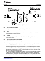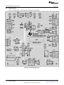
1
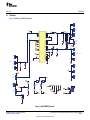
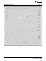
User's Guide
SLUUBB5A – April 2015 – Revised October 2015
User's Guide for WCSP-Packaged bq24261M 3-A Battery
Charger Evaluation Module
The bq24261M evaluation module is a complete charger module for evaluating compact, flexible, highefficiency, USB-friendly, switch-mode charge management solutions for single-cell, Li-ion and Li-polymer
batteries used in a wide range of portable applications.
1
2
3
4
Contents
Introduction ................................................................................................................... 2
1.1
bq24261M IC Features............................................................................................. 2
1.2
bq24261M EVM Features ......................................................................................... 2
1.3
Schematic ............................................................................................................ 3
1.4
I/O Description ...................................................................................................... 4
1.5
Test Points ........................................................................................................... 4
1.6
Control and Key Parameters Setting ............................................................................. 5
1.7
Recommended Operating Conditions ............................................................................ 5
Test Summary ................................................................................................................ 6
2.1
Definitions ............................................................................................................ 6
2.2
Recommended Test Equipment .................................................................................. 6
2.3
Recommended Test Equipment Setup .......................................................................... 8
2.4
Recommended Test Procedure ................................................................................. 10
Printed-Circuit Board Layout Guideline.................................................................................. 12
Bill of Materials and Board Layout ...................................................................................... 13
4.1
Bill of Materials .................................................................................................... 13
4.2
Board Layout ....................................................................................................... 14
List of Figures
1
bq24261MEVM Schematic ................................................................................................. 3
2
BAT_Load (PR1010) Schematic ........................................................................................... 7
3
Connections of HPA172 Kit
4
Original Test Setup for bq24261MEVM-691 ............................................................................. 9
5
Main Window of bq24261MSW Evaluation Software .................................................................. 10
6
Top Assembly Layer ....................................................................................................... 14
7
Top Layer
8
9
10
11
................................................................................................
...................................................................................................................
First Internal Layer .........................................................................................................
Second Internal Layer .....................................................................................................
Bottom Layer ................................................................................................................
Bottom Assembly Drawing ................................................................................................
8
15
16
17
18
19
List of Tables
1
Bill of Materials - bq24261MEVM-691
SLUUBB5A – April 2015 – Revised October 2015
Submit Documentation Feedback
..................................................................................
User's Guide for WCSP-Packaged bq24261M 3-A Battery Charger
Evaluation Module
Copyright © 2015, Texas Instruments Incorporated
13
1
Introduction
1
Introduction
1.1
bq24261M IC Features
www.ti.com
The bq24261M device integrates a synchronous PWM controller, power MOSFETs, input-current sensing,
high-accuracy current and voltage regulation, charge termination and power path management into a
small WCSP package. The charge parameters can be programmed through an I2C interface. Key IC
features include:
• High-efficiency, fully-integrated, NMOS-NMOS, synchronous buck charger with 1.5-MHz frequency
• Charge time optimizer
• Integrated power FETs for up to 3-A charge rate
• 5-V, 1-A OTG VBUS supply
• Power path management between battery and system voltages
For details, see the bq24261M data sheet (SLUSC09).
1.2
bq24261M EVM Features
The bq24261M evaluation module (EVM) on PCB PWR691 provide a complete charger module for
evaluating compact, flexible, high-efficiency, USB-friendly, switch-mode battery charge and power path
management solution for single-cell, Li-ion and Li-polymer battery-powered systems used in a wide range
of portable applications. Key EVM features include:
• Terminal blocks and standard headers for IN, SYS, BAT, TS
• Programmable battery voltage, charge current, input current, and status via I2C interface
• IN operating up to 10.5 V for bq24261M
• LED indication for status signals
• Test points for key signals available for testing purposes. Easy probe hook-up
2
User's Guide for WCSP-Packaged bq24261M 3-A Battery Charger
Evaluation Module
Copyright © 2015, Texas Instruments Incorporated
SLUUBB5A – April 2015 – Revised October 2015
Submit Documentation Feedback
Introduction
www.ti.com
1.3
Schematic
Figure 1 illustrates the bq24261M schematic.
SYS
J11
SYS
GND
U1
IN
C1
C2
C3
C4
L1
IN
IN
IN
IN
SW
SW
SW
SW
SW
SYS
SW
B2
B3
B4
B5
B6
ED555/2DS
J10
SPM4012T-1R5M
GND
R8
1.00M
C3
0.033µF
SDA
SCL
INT
STAT
PSEL
BGATE
SDA
SCL
E2
INT
E1
STAT
D4
PSEL
F2
BGATE
NC
B1
J4
PMID
1µF
GND
J1
IN
1
SYS
SYS
SYS
SYS
BAT
BAT
BAT
BAT
F3
F4
F5
F6
TS
D5
DRV
D6
PGND
PGND
PGND
PGND
PGND
PGND
GND
C6
E3
E4
E5
E6
AGND
C7
IN
GND
BOOT
D1
D2
D3
DM
up to 6V, 3A
CD
JP4
C5
22µF
2
GATE
Q1
CSD25402Q3A
GND
SYS (OFF)
BGATE
3
C5
BGATE
BAT
J13
BAT
TS
C4
1µF
DRV
BAT
GND
C2
1µF
A1
A2
A3
A4
A5
A6
J14
DNPC6
10µF
F1
GND
up to 4.44V, 3A
ED555/2DS
GND
J5
GND
GND
bq24261M
DNP C8
10µF
GND
GND
C1
1µF
ED555/2DS
J6
DRV
GND
GND
J8
GND
J7
GND
DRV
DRV
GND
ED555/2DS
1
DRV
J3
HIGH
CD
LOW
JP5
2
GND
DRV
JP3
3
JP2
GND
DRV
J9
R5
5.62k
GND
EXT TS
ED555/2DS
D1
GreenSTAT
GND
D2
Red INT
TP2
1
TP1
TP4
TP5
TP7
TP3
TP9
R6
12.4k
JP6
EXT
TS
SIM
J15
SW
TS
2
R3
R4
1.50k
1.50k
SCL
200
BAT
STAT
3
TP10
GND
GND
SYS
TP6
R2
IN
INT
SDA
R1
1
2
3
4
GND
22-05-3041
200 TP11
TP8
GND
R7
100k
GND
Figure 1. bq24261MEVM Schematic
SLUUBB5A – April 2015 – Revised October 2015
Submit Documentation Feedback
User's Guide for WCSP-Packaged bq24261M 3-A Battery Charger Evaluation
Module
Copyright © 2015, Texas Instruments Incorporated
3
Introduction
1.4
1.5
4
www.ti.com
I/O Description
Header/Terminal Block
Description
J1– IN/GND
Input power positive and negative terminal
J2 – Do not use
Do not use
J3 - GND
DRV linear regulator negative header
J4 - IN
Input power positive header
J5 - GND
Battery negative header
J6 - DRV
DRV linear regulator positive output
J7 - DRV/GND
DRV linear regulator positive and negative terminals
J8 - GND
Input power negative header
J9 - EXT TS/GND
External thermistor terminal
J10 - GND
SYS output negative header
J11 - SYS/GND
SYS output positive and negative terminal
J12 - SYS
SYS output positive header
J13 - BAT
Battery positive header
J14 - BAT/GND
Battery positive and negative header
J15 - USB-to-GPIO
USB-to-GPIO box keyed connector
Test Points
Test Point
Description
TP1
BAT
TP2
SW
TP3
GND
TP4
SYS
TP5
IN
TP6
STAT
TP7
GND
TP8
INT
TP9
TS
TP10
SCL
TP11
SDA
User's Guide for WCSP-Packaged bq24261M 3-A Battery Charger
Evaluation Module
Copyright © 2015, Texas Instruments Incorporated
SLUUBB5A – April 2015 – Revised October 2015
Submit Documentation Feedback
Introduction
www.ti.com
1.6
1.7
Control and Key Parameters Setting
Jumper
Description
Default Factory Setting
JP1
Leave jumper open
OPEN
JP2
Shorting jumper to connect DRV to anode of D1 STAT LED
SHORTED
JP3
Shorting jumper to connect DRV to anode of D1 INT LED
SHORTED
JP4
GATE = SYS: External PFET's gate tied to SYS and therefore disabled.
GATE = BGATE: External PFET's gate tied to BGATE pin and therefore controlled by
IC.
GATE=BGATE
JP5
CD = LO: Charge disable low for normal operation
CD = HI: Charge disable high to disable the buck converter and enter Hi-Z mode
CD = LO
JP6
TS = SIM: Connects a potentiometer to the TS pin so that the potentiometer can
simulator a thermistor. The potentiometer has been preset per R5 and R6 so that the
TS voltage is 0.5 x V (DRV).
TS = EXT: Connects the TS pin to an external thermistor through J9. The resistor
divider formed by R5 and R6 has been sized to accommodate a 10-kΩ thermistor. If a
different thermistor is used, R5 and R6 must be resized.
TS=SIM
JP7
PSEL = LO: Input current limit is set to 1.5 A until changed by I2C.
PSEL = HI: Input current limit is set to USB100 until changed by I2C.
PSEL = HI
Recommended Operating Conditions
Min
Typ
Max
Unit
Supply voltage, VIN
Input voltage from ac adapter
4.2
10.0
V
System voltage, VSYS
Voltage output at SYS terminal ; depends on VBAT voltage
and status of VINDPM)
3.4
VBATR
EG+3%
V
Battery voltage, VBAT
Voltage output at VBAT terminal (registers set via I2C
communication)
1.9
4.44
V
Supply current, IIN(MAX)
Maximum input current from ac adapter input (registers set
via I2C communication)
0.1
2.5
A
Fast charge current,
ICHRG(MAX)
Battery charge current (registers set via I2C communication)
0.500
3.0
A
-40
125
°C
Operating junction temperature range, TJ
SLUUBB5A – April 2015 – Revised October 2015
Submit Documentation Feedback
4.2
User's Guide for WCSP-Packaged bq24261M 3-A Battery Charger
Evaluation Module
Copyright © 2015, Texas Instruments Incorporated
5
Test Summary
2
www.ti.com
Test Summary
This procedure describes one test configuration of the bq24261MEVM-691 evaluation board for bench
evaluation.
2.1
Definitions
The following naming conventions are followed.
VXXX :
LOADW:
V(TPyyy):
V(Jxx):
V(TP(XXX)):
V(XXX, YYY):
I(JXX(YYY)):
Jxx(BBB):
JPx ON :
JPx OFF:
JPx (-YY-)
Measure: → A,B
Observe → A,B
External voltage supply name (VADP, VBT, VSBT)
External load name (LOAD1, LOAD2)
Voltage at internal test point TPyyy. For example, V(TP12) means the voltage at
TP12.
Voltage at header Jxx
Voltage at test point XXX. For example, V(ACDET) means the voltage at the test
point which is marked as ACDET.
Voltage across point XXX and YYY.
Current going out from the YYY terminal of header XX.
Terminal or pin BBB of header xx.
Internal jumper Jxx terminals are shorted.
Internal jumper Jxx terminals are open.
ON: Internal jumper Jxx adjacent terminals marked as YY are shorted.
Check specified parameters A, B. If measured values are not within specified limits,
the unit under test has failed.
Observe if A, B occur. If they do not occur, the unit under test has failed.
Assembly drawings have location for jumpers, test points, and individual components.
2.2
Recommended Test Equipment
2.2.1
Power Supplies
1. Power Supply #1 (PS #1) capable of supplying 6 V at 2 A is required.
2. If not using a battery as the load, then power supply #2 (PS #2) capable of supplying up to 5 V at 5 A
is required to power the circuit shown in Figure 2.
2.2.2
Load #1 Between BAT and GND
Testing with an actual battery is the best way to verify operation in the system. If a battery is not available,
then a circuit similar to the one shown in Figure 2 can simulate a battery when connected to a power
supply.
6
User's Guide for WCSP-Packaged bq24261M 3-A Battery Charger
Evaluation Module
Copyright © 2015, Texas Instruments Incorporated
SLUUBB5A – April 2015 – Revised October 2015
Submit Documentation Feedback
Test Summary
www.ti.com
Figure 2. BAT_Load (PR1010) Schematic
2.2.3
Load #2 Between SYS and GND
Although not required, a resistive load capable of sinking up to 3 A can be used.
2.2.4
Meters
Four equivalent voltage meters (VM #) and two equivalent current meters (CM #) are required. The current
meters must be able to measure 2-A current.
2.2.5
Computer
A computer with at least one USB port and a USB cable is required. The bq24261M evaluation software
must be properly installed.
2.2.6
HPA172 Communication Kit (USB TO GPIO)
An HPA172 USB-to-I2C communication kit is required.
2.2.7
Software
Download Battery Management Studio.zip from the charger's product folder, unzip the file, and doubleclick on the SETUP.EXE file. Follow the installation steps.
Because the bq24261M has the watchdog timers enabled, it is recommended that you set the software's
Reset Watchdog Timer to reset every 5 seconds. Otherwise, after 30 seconds of operation, the IC enters
Default mode. Note that the 27-minute safety timer is not reset by this function and eventually times out if
charging does not complete, unless the Safety Timer Time Limit is expanded or disabled via the GUI.
One way to reset the safety timer is to allow the 30-second watchdog timer to expire. See Figure 3 in the
data sheet for more information about the timers.
Also, it is generally helpful to activate the Write On Change functions, in the upper left of the GUI window,
to ON. The Write On Change function writes any changes to the GUI's check boxes, drop-down boxes,
and registers to the IC. Otherwise, the user must click the WRITE button to write changes to the software.
It is recommended that the user periodically click the READ button to find the IC's instantaneous status.
Alternatively, the AutoRead function can be activated to periodically update the GUI with the IC's status.
SLUUBB5A – April 2015 – Revised October 2015
Submit Documentation Feedback
User's Guide for WCSP-Packaged bq24261M 3-A Battery Charger
Evaluation Module
Copyright © 2015, Texas Instruments Incorporated
7
Test Summary
2.3
www.ti.com
Recommended Test Equipment Setup
1. For all power connections, use short, twisted-pair wires of appropriate gauge wire for the amount of the
current.
2. Set power supply #1 (PS #1) for 6-V, 2-A current limit and then turn off supply.
3. If BAT_Load as shown in Figure 1 is used, connect Power Supply #2 (PS #2) set to approximately 3.6
V to the input side (PS #2+/-) of BAT_Load, then turn off PS #2.
4. Connect the output side of the battery or BAT_Load in series with current meter (multimeter) #2 (CM
#2) to J2 and J6 or J3 (BAT, GND). Ensure that a voltage meter is connected across J2 or TP3 and J6
or TP9 (BAT, GND).
5. Connect VM #3 across J10 or TP7 and J14 or TP9 (SYS, GND).
6. Connect VM #4 across J15 or TP5 and J14 or TP9 (DRV, GND).
7. Connect J17 to EV2400 kit by the 4-pin ribbon cable. Connect the USB port of the EV2400 kit to the
USB port of the computer. The connections are shown in Figure 3.
Figure 3. Connections of HPA172 Kit
8. Ensure jumpers are at the default factory settings per Section 1.6.
9. After the preceding steps have been performed, the test setup for bq24261MEVM-691 is configured as
is shown in Figure 4.
8
User's Guide for WCSP-Packaged bq24261M 3-A Battery Charger
Evaluation Module
Copyright © 2015, Texas Instruments Incorporated
SLUUBB5A – April 2015 – Revised October 2015
Submit Documentation Feedback
Test Summary
www.ti.com
Figure 4. Original Test Setup for bq24261MEVM-691
10. Turn on the computer. Open the bq24261M evaluation software. The main window of the software is
shown in Figure 5.
SLUUBB5A – April 2015 – Revised October 2015
Submit Documentation Feedback
User's Guide for WCSP-Packaged bq24261M 3-A Battery Charger
Evaluation Module
Copyright © 2015, Texas Instruments Incorporated
9
Test Summary
www.ti.com
Figure 5. Main Window of bq24261MSW Evaluation Software
2.4
Recommended Test Procedure
The following test procedure may be useful for evaluating the charger IC outside of a real system, if no
battery is available to connect to the output and a simulated battery if needed.
2.4.1
Charge Voltage and Current Regulation of IN in HOST mode
1. Ensure that the Section 2.3 steps are followed.
2. Ensure that the shunts are installed as highlighted in yellow in Figure 4.
3. Connect the output of Power Supply #1 (PS #1), with at least a 4-A current limit setting, in series with
current meter (multimeter) #1 (CM #1) to J1 as shown in Figure 4.
4. Connect voltage meter 1 (VM #1) across J4 and J3 or TP5 and or TP7 (IN, GND).
5. Connect either a real single cell lithium ion battery or battery simulator across J14 or J13/J5 (BAT,
GND) with current meter #2 in series as shown in Figure 4. If using a battery simulator like the one
shown in Figure 2and referred to as BAT_LOAD in Figure 4, configure power supply #2 (PS#2) with at
least 4-A current limit for 3.4 V.
6. Install voltage meter #1 (VM #1) across J4 and J3 or TP5 and TP7 (IN and GND).
7. Install voltage meter #2 (VM #2) across J13 and J5 or TP1 and TP7 (BAT and GND).
8. Install voltage meter #3 (VM #3) across J12 and J10 or TP4 and TP7 (SYS and GND).
9. Voltage meter #4 is optional.
10. Turn on PS #1 and PS #2 if used.
11. Software setup:
• Press the READ button to obtain the current settings.
• Set Write On Change to ON if not already set.
• Set Reset Watchdog Timer to reset every 5 seconds.
• Uncheck Disable Charging if checked.
• Check Enable STAT/INT Outputs.
10
User's Guide for WCSP-Packaged bq24261M 3-A Battery Charger
Evaluation Module
Copyright © 2015, Texas Instruments Incorporated
SLUUBB5A – April 2015 – Revised October 2015
Submit Documentation Feedback
Test Summary
www.ti.com
• Set Battery Regulation Voltage to 4.20 V.
• Set Input Current Limit to 2.5 A.
• Set Charge Current to 2000 mA.
• Click the READ button at the top of the window and confirm that the previous settings remain.
12. To test charge current regulation, adjust the PS #1 power supply so that VM #1 still reads 5 V and
PS#2 so that the voltage measured by VM#2 is 3.6 V.
Measure on CM#2 → ICHRG = 2000 mA ±100 mA
Measure on CM#1 → IIN < 1600 mA.
13. To test input current limit, lower the software's Input Current Limit setting to 900 mA then readjust PS
#1 so that VM #1 reads 5 V and PS#2 reads 3.6 V.
Measure on CM#2 → ICHRG < 2000 mA.
Measure on CM#1 → IIN = 800 mA – 900 mA .
14. To test minimum system voltage and DPPM, return the software's Input Current Limit setting to 2500
mA then lower PS #2 until VM#2 reads 3.3 V. Add an external resistive or constant current load across
J13 and J5 that does not draw more than 2.5 A from SYS.
Measure on VM#3 → 3.44 V – 3.55 V.
Measure on CM#2 → ICHRG = 2000 mA ±100 mA minus the load current on SYS.
15. To test VINDPM function, remove the load on SYS, adjust PS#1 so that VM#1 reads 5 V, adjust PS# 2
so that VM#2 reads 3.6 V and then lower the current limit setting on PS#1 to below the software's
Charge Current setting.
Measure on VM#1 → VIN = software's V INDPM level (default of 4.2 V).
Measure on CM#2 → ICHRG < 2000 mA.
16. To test battery regulation and charge termination, return the PS#1 current limit to 4-A and confirm that
the software's Enable Termination box is checked then slowly increase PS#2 until VM#2 reaches 4.2
V.
Measure on CM#2 → ICHRG slowly tapers to the software's ITERM setting (default of 150 mA) and then
drops to zero.
Observe → LEDs turn off.
17. To test battery supplement mode, lower PS #2 until VM#2 reads 3.6 V. Add an external resistive or
constant current load across J13 and J5 that draws more than 2 A from SYS.
Measure on VM#4 → 3.6 V - IBATSUP × RDSON(BATFET).
Measure on #2 → ICHRG = - IBATSUP
18. Turn off PS #1 and PS #2.
2.4.2
Helpful Hints
1. The leads/cables to the various power supplies have resistance. The current meters also have series
resistance. Therefore, you must use voltmeters to measure the voltage as close to the IC pins as
possible instead of relying on the supplies digital readouts.
2. When using a sourcemeter that can source and sink current as your battery simulator, it is highly
recommended to add a large (1000 µF+) capacitor at the EVM BAT and GND connectors in order to
prevent oscillations at the BAT pin due to mismatched impedances of the charger output and
sourcemeter input within their respective regulation loop bandwidths. Configuring the sourcemeter for
4-wire sensing eliminates the need for a separate voltmeter to measure the voltage at the BAT pin.
When using 4-wire sensing, always ensure that the sensing leads are connected first in order to
prevent accidental overvoltage by the power leads.
3. For precise measurements of charge current and battery regulation near termination, the current meter
in series with the battery or battery simulator must be removed. An alternate method for measuring
charge current is to either use an oscilloscope with hall effect current probe or place a 1% or better,
thermally capable (for example, 0.010 Ω in 1206 or larger footprint) resistor in series between the BAT
pin and battery and measure the voltage across that resistor.
SLUUBB5A – April 2015 – Revised October 2015
Submit Documentation Feedback
User's Guide for WCSP-Packaged bq24261M 3-A Battery Charger
Evaluation Module
Copyright © 2015, Texas Instruments Incorporated
11
Printed-Circuit Board Layout Guideline
3
www.ti.com
Printed-Circuit Board Layout Guideline
1. To obtain optimal performance, the power input capacitors, connected from the PMID input to PGND,
must be placed as close as possible to the IC.
2. Place 4.7-µF input capacitor as close to PMID pin and PGND pin as possible to make the highfrequency current loop area as small as possible. Place 1-µF input capacitor GNDs as close to the
respective PMID capacitor GND and PGND pins as possible to minimize the ground difference
between the input and PMID.
3. The local bypass capacitor from SYS to GND must be connected between the SYS pin and PGND of
the IC. The intent is to minimize the current path loop area from the SW pin through the LC filter and
back to the PGND pin.
4. Place all decoupling capacitors close to their respective IC pins and as close as to PGND (do not place
components such that routing interrupts power stage currents). All small control signals must be routed
away from the high-current paths.
5. The PCB must have a ground plane (return) connected directly to the return of all components through
vias (two vias per capacitor for power-stage capacitors, one via per capacitor for small-signal
components). It is also recommended to put vias inside the PGND pads for the IC, if possible. A star
ground design approach is typically used to keep circuit block currents isolated (high-power/low-power
small-signal) which reduces noise-coupling and ground-bounce issues. A single ground plane for this
design gives good results. With this small layout and a single ground plane, no ground-bounce issue
exists, and having the components segregated minimizes coupling between signals.
6. The high-current charge paths into IN, USB, BAT, SYS, and from the SW pins must be sized
appropriately for the maximum charge current in order to avoid voltage drops in these traces. The
PGND pins must be connected to the ground plane to return current through the internal low-side FET.
7. For high-current applications, the balls for the power paths must be connected to as much copper in
the board as possible. This allows better thermal performance because the board conducts heat away
from the IC.
12
User's Guide for WCSP-Packaged bq24261M 3-A Battery Charger
Evaluation Module
Copyright © 2015, Texas Instruments Incorporated
SLUUBB5A – April 2015 – Revised October 2015
Submit Documentation Feedback
Bill of Materials and Board Layout
www.ti.com
4
Bill of Materials and Board Layout
4.1
Bill of Materials
Table 1 lists the bill of materials for this EVM.
Table 1. Bill of Materials - bq24261MEVM-691
Designator
Description
Manufacturer
PartNumber
Qty
!PCB
Printed Circuit Board
Any
PWR691
1
C1
CAP, CERM, 4.7 µF, 25 V, +/- 20%, X5R, 0402
MuRata
GRM155R61E475ME15
1
C2
CAP, CERM, 1 µF, 10 V, +/- 10%, X7S, 0402
TDK
C1005X7S1A105K050BC
1
C3
CAP, CERM, 0.033 µF, 25 V, +/- 10%, X7R, 0402
MuRata
GRM155R71E333KA88D
1
C4
CAP, CERM, 1 µF, 10 V, +/- 10%, X5R, 0402
MuRata
GRM155R61A105KE15D
1
C5
CAP, CERM, 22 µF, 10 V, +/- 20%, X5R, SMD, 2-Leads, Body 1.6x0.8mm
TDK
C1608X5R1A226M080AC
1
C9
CAP, CERM, 1 µF, 25 V, +/- 10%, X5R, 0402
TDK
C1005X5R1E105K050BC
1
D1
LED, Green, SMD
Lite-On
LTST-C190GKT
1
D2
LED, Red, SMD
Lite-On
LTST-C190CKT
1
J1, J7, J9, J11, J14
Terminal Block, 6A, 3.5mm Pitch, 2-Pos, TH
On-Shore Technology
ED555/2DS
5
J2
Connector, Receptacle, Micro-USB Type AB, R/A, Bottom Mount SMT
Molex
0475890001
1
J3, J4, J5, J6, J8, J10, J12, J13, JP1, JP2, JP3
Header, 100mil, 2x1, TH
Mill-Max
800-10-002-10-001000
11
J15
Header (friction lock), 100mil, 4x1, R/A, TH
Molex
22-05-3041
1
JP4, JP5
Header, 100mil, 3x1, TH
Mill-Max
800-10-003-10-001000
2
L1
Inductor, Wirewound, Metal Composite, 1.5 µH, 3.5 A, 0.07 ohm, SMD
TDK
SPM4012T-1R5M
1
LBL1
Thermal Transfer Printable Labels, 0.650" W x 0.200" H - 10,000 per roll
Brady
THT-14-423-10
1
Q1
MOSFET, P-CH, -20 V, -60 A, SON 3.3x3.3mm
Texas Instruments
CSD25401Q3
1
R1, R2
RES, 200 ohm, 1%, 0.1W, 0603
Vishay-Dale
CRCW0603200RFKEA
2
R3, R4
RES, 1.50k ohm, 1%, 0.1W, 0603
Yageo America
RC0603FR-071K5L
2
R5
RES, 5.62k ohm, 1%, 0.063W, 0402
Vishay-Dale
CRCW04025K62FKED
1
R6
RES, 12.4k ohm, 1%, 0.063W, 0402
Vishay-Dale
CRCW040212K4FKED
1
R7
Trimmer, 100k ohm, 0.25W, TH
Bourns
3266W-1-104LF
1
R8
RES, 1.00 M, 1%, 0.1 W, 0603
Vishay-Dale
CRCW06031M00FKEA
1
R9
RES, 0 ohm, 5%, 0.063W, 0402
Vishay-Dale
CRCW04020000Z0ED
1
SH-JP1, SH-JP2, SH-JP3, SH-JP4, SH-JP5
Shunt, 100mil, Gold plated, Black
3M
969102-0000-DA
5
TP1, TP5
Test Point, Miniature, Red, TH
Keystone
5000
2
TP2, TP4, TP6, TP8, TP9, TP10, TP11
Test Point, Miniature, White, TH
Keystone
5002
7
TP3, TP7
Test Point, Miniature, Black, TH
Keystone
5001
2
U1
3A, 30V, Host-Controlled Single-Input, Single Cell Switchmode Li-Ion Battery Charger
with Power Path Management and USB-OTG Support, YFF0036ADAD
Texas Instruments
bq24261MYFF
1
SLUUBB5A – April 2015 – Revised October 2015
Submit Documentation Feedback
User's Guide for WCSP-Packaged bq24261M 3-A Battery Charger Evaluation
Module
Copyright © 2015, Texas Instruments Incorporated
13
Bill of Materials and Board Layout
4.2
www.ti.com
Board Layout
Figure 6 through Figure 11 illustrate the PCB layouts for this EVM.
Figure 6. Top Assembly Layer
14
User's Guide for WCSP-Packaged bq24261M 3-A Battery Charger
Evaluation Module
Copyright © 2015, Texas Instruments Incorporated
SLUUBB5A – April 2015 – Revised October 2015
Submit Documentation Feedback
Bill of Materials and Board Layout
www.ti.com
Figure 7. Top Layer
SLUUBB5A – April 2015 – Revised October 2015
Submit Documentation Feedback
User's Guide for WCSP-Packaged bq24261M 3-A Battery Charger
Evaluation Module
Copyright © 2015, Texas Instruments Incorporated
15
Bill of Materials and Board Layout
www.ti.com
Figure 8. First Internal Layer
16
User's Guide for WCSP-Packaged bq24261M 3-A Battery Charger
Evaluation Module
Copyright © 2015, Texas Instruments Incorporated
SLUUBB5A – April 2015 – Revised October 2015
Submit Documentation Feedback
Bill of Materials and Board Layout
www.ti.com
Figure 9. Second Internal Layer
SLUUBB5A – April 2015 – Revised October 2015
Submit Documentation Feedback
User's Guide for WCSP-Packaged bq24261M 3-A Battery Charger
Evaluation Module
Copyright © 2015, Texas Instruments Incorporated
17
Bill of Materials and Board Layout
www.ti.com
Figure 10. Bottom Layer
18
User's Guide for WCSP-Packaged bq24261M 3-A Battery Charger
Evaluation Module
Copyright © 2015, Texas Instruments Incorporated
SLUUBB5A – April 2015 – Revised October 2015
Submit Documentation Feedback
Bill of Materials and Board Layout
www.ti.com
Figure 11. Bottom Assembly Drawing
SLUUBB5A – April 2015 – Revised October 2015
Submit Documentation Feedback
User's Guide for WCSP-Packaged bq24261M 3-A Battery Charger
Evaluation Module
Copyright © 2015, Texas Instruments Incorporated
19
Revision History
www.ti.com
Revision History
Changes from Original (April 2015) to A Revision .......................................................................................................... Page
•
•
•
Deleted text "USB connector for IN" from bq24261M EVM Features .............................................................. 2
Deleted the USB miniconnector from the schematic in Figure 1.................................................................... 3
Changed J2 – USB To: J2 – Do not use in Section 1.4.............................................................................. 4
NOTE: Page numbers for previous revisions may differ from page numbers in the current version.
20
Revision History
SLUUBB5A – April 2015 – Revised October 2015
Submit Documentation Feedback
Copyright © 2015, Texas Instruments Incorporated
STANDARD TERMS AND CONDITIONS FOR EVALUATION MODULES
1.
Delivery: TI delivers TI evaluation boards, kits, or modules, including any accompanying demonstration software, components, or
documentation (collectively, an “EVM” or “EVMs”) to the User (“User”) in accordance with the terms and conditions set forth herein.
Acceptance of the EVM is expressly subject to the following terms and conditions.
1.1 EVMs are intended solely for product or software developers for use in a research and development setting to facilitate feasibility
evaluation, experimentation, or scientific analysis of TI semiconductors products. EVMs have no direct function and are not
finished products. EVMs shall not be directly or indirectly assembled as a part or subassembly in any finished product. For
clarification, any software or software tools provided with the EVM (“Software”) shall not be subject to the terms and conditions
set forth herein but rather shall be subject to the applicable terms and conditions that accompany such Software
1.2 EVMs are not intended for consumer or household use. EVMs may not be sold, sublicensed, leased, rented, loaned, assigned,
or otherwise distributed for commercial purposes by Users, in whole or in part, or used in any finished product or production
system.
2
Limited Warranty and Related Remedies/Disclaimers:
2.1 These terms and conditions do not apply to Software. The warranty, if any, for Software is covered in the applicable Software
License Agreement.
2.2 TI warrants that the TI EVM will conform to TI's published specifications for ninety (90) days after the date TI delivers such EVM
to User. Notwithstanding the foregoing, TI shall not be liable for any defects that are caused by neglect, misuse or mistreatment
by an entity other than TI, including improper installation or testing, or for any EVMs that have been altered or modified in any
way by an entity other than TI. Moreover, TI shall not be liable for any defects that result from User's design, specifications or
instructions for such EVMs. Testing and other quality control techniques are used to the extent TI deems necessary or as
mandated by government requirements. TI does not test all parameters of each EVM.
2.3 If any EVM fails to conform to the warranty set forth above, TI's sole liability shall be at its option to repair or replace such EVM,
or credit User's account for such EVM. TI's liability under this warranty shall be limited to EVMs that are returned during the
warranty period to the address designated by TI and that are determined by TI not to conform to such warranty. If TI elects to
repair or replace such EVM, TI shall have a reasonable time to repair such EVM or provide replacements. Repaired EVMs shall
be warranted for the remainder of the original warranty period. Replaced EVMs shall be warranted for a new full ninety (90) day
warranty period.
3
Regulatory Notices:
3.1 United States
3.1.1
Notice applicable to EVMs not FCC-Approved:
This kit is designed to allow product developers to evaluate electronic components, circuitry, or software associated with the kit
to determine whether to incorporate such items in a finished product and software developers to write software applications for
use with the end product. This kit is not a finished product and when assembled may not be resold or otherwise marketed unless
all required FCC equipment authorizations are first obtained. Operation is subject to the condition that this product not cause
harmful interference to licensed radio stations and that this product accept harmful interference. Unless the assembled kit is
designed to operate under part 15, part 18 or part 95 of this chapter, the operator of the kit must operate under the authority of
an FCC license holder or must secure an experimental authorization under part 5 of this chapter.
3.1.2
For EVMs annotated as FCC – FEDERAL COMMUNICATIONS COMMISSION Part 15 Compliant:
CAUTION
This device complies with part 15 of the FCC Rules. Operation is subject to the following two conditions: (1) This device may not
cause harmful interference, and (2) this device must accept any interference received, including interference that may cause
undesired operation.
Changes or modifications not expressly approved by the party responsible for compliance could void the user's authority to
operate the equipment.
FCC Interference Statement for Class A EVM devices
NOTE: This equipment has been tested and found to comply with the limits for a Class A digital device, pursuant to part 15 of
the FCC Rules. These limits are designed to provide reasonable protection against harmful interference when the equipment is
operated in a commercial environment. This equipment generates, uses, and can radiate radio frequency energy and, if not
installed and used in accordance with the instruction manual, may cause harmful interference to radio communications.
Operation of this equipment in a residential area is likely to cause harmful interference in which case the user will be required to
correct the interference at his own expense.
SPACER
SPACER
SPACER
SPACER
SPACER
SPACER
SPACER
SPACER
FCC Interference Statement for Class B EVM devices
NOTE: This equipment has been tested and found to comply with the limits for a Class B digital device, pursuant to part 15 of
the FCC Rules. These limits are designed to provide reasonable protection against harmful interference in a residential
installation. This equipment generates, uses and can radiate radio frequency energy and, if not installed and used in accordance
with the instructions, may cause harmful interference to radio communications. However, there is no guarantee that interference
will not occur in a particular installation. If this equipment does cause harmful interference to radio or television reception, which
can be determined by turning the equipment off and on, the user is encouraged to try to correct the interference by one or more
of the following measures:
•
•
•
•
Reorient or relocate the receiving antenna.
Increase the separation between the equipment and receiver.
Connect the equipment into an outlet on a circuit different from that to which the receiver is connected.
Consult the dealer or an experienced radio/TV technician for help.
3.2 Canada
3.2.1
For EVMs issued with an Industry Canada Certificate of Conformance to RSS-210
Concerning EVMs Including Radio Transmitters:
This device complies with Industry Canada license-exempt RSS standard(s). Operation is subject to the following two conditions:
(1) this device may not cause interference, and (2) this device must accept any interference, including interference that may
cause undesired operation of the device.
Concernant les EVMs avec appareils radio:
Le présent appareil est conforme aux CNR d'Industrie Canada applicables aux appareils radio exempts de licence. L'exploitation
est autorisée aux deux conditions suivantes: (1) l'appareil ne doit pas produire de brouillage, et (2) l'utilisateur de l'appareil doit
accepter tout brouillage radioélectrique subi, même si le brouillage est susceptible d'en compromettre le fonctionnement.
Concerning EVMs Including Detachable Antennas:
Under Industry Canada regulations, this radio transmitter may only operate using an antenna of a type and maximum (or lesser)
gain approved for the transmitter by Industry Canada. To reduce potential radio interference to other users, the antenna type
and its gain should be so chosen that the equivalent isotropically radiated power (e.i.r.p.) is not more than that necessary for
successful communication. This radio transmitter has been approved by Industry Canada to operate with the antenna types
listed in the user guide with the maximum permissible gain and required antenna impedance for each antenna type indicated.
Antenna types not included in this list, having a gain greater than the maximum gain indicated for that type, are strictly prohibited
for use with this device.
Concernant les EVMs avec antennes détachables
Conformément à la réglementation d'Industrie Canada, le présent émetteur radio peut fonctionner avec une antenne d'un type et
d'un gain maximal (ou inférieur) approuvé pour l'émetteur par Industrie Canada. Dans le but de réduire les risques de brouillage
radioélectrique à l'intention des autres utilisateurs, il faut choisir le type d'antenne et son gain de sorte que la puissance isotrope
rayonnée équivalente (p.i.r.e.) ne dépasse pas l'intensité nécessaire à l'établissement d'une communication satisfaisante. Le
présent émetteur radio a été approuvé par Industrie Canada pour fonctionner avec les types d'antenne énumérés dans le
manuel d’usage et ayant un gain admissible maximal et l'impédance requise pour chaque type d'antenne. Les types d'antenne
non inclus dans cette liste, ou dont le gain est supérieur au gain maximal indiqué, sont strictement interdits pour l'exploitation de
l'émetteur
3.3 Japan
3.3.1
Notice for EVMs delivered in Japan: Please see http://www.tij.co.jp/lsds/ti_ja/general/eStore/notice_01.page 日本国内に
輸入される評価用キット、ボードについては、次のところをご覧ください。
http://www.tij.co.jp/lsds/ti_ja/general/eStore/notice_01.page
3.3.2
Notice for Users of EVMs Considered “Radio Frequency Products” in Japan: EVMs entering Japan may not be certified
by TI as conforming to Technical Regulations of Radio Law of Japan.
If User uses EVMs in Japan, not certified to Technical Regulations of Radio Law of Japan, User is required by Radio Law of
Japan to follow the instructions below with respect to EVMs:
1.
2.
3.
Use EVMs in a shielded room or any other test facility as defined in the notification #173 issued by Ministry of Internal
Affairs and Communications on March 28, 2006, based on Sub-section 1.1 of Article 6 of the Ministry’s Rule for
Enforcement of Radio Law of Japan,
Use EVMs only after User obtains the license of Test Radio Station as provided in Radio Law of Japan with respect to
EVMs, or
Use of EVMs only after User obtains the Technical Regulations Conformity Certification as provided in Radio Law of Japan
with respect to EVMs. Also, do not transfer EVMs, unless User gives the same notice above to the transferee. Please note
that if User does not follow the instructions above, User will be subject to penalties of Radio Law of Japan.
SPACER
SPACER
SPACER
SPACER
SPACER
【無線電波を送信する製品の開発キットをお使いになる際の注意事項】 開発キットの中には技術基準適合証明を受けて
いないものがあります。 技術適合証明を受けていないもののご使用に際しては、電波法遵守のため、以下のいずれかの
措置を取っていただく必要がありますのでご注意ください。
1.
2.
3.
電波法施行規則第6条第1項第1号に基づく平成18年3月28日総務省告示第173号で定められた電波暗室等の試験設備でご使用
いただく。
実験局の免許を取得後ご使用いただく。
技術基準適合証明を取得後ご使用いただく。
なお、本製品は、上記の「ご使用にあたっての注意」を譲渡先、移転先に通知しない限り、譲渡、移転できないものとします。
上記を遵守頂けない場合は、電波法の罰則が適用される可能性があることをご留意ください。 日本テキサス・イ
ンスツルメンツ株式会社
東京都新宿区西新宿6丁目24番1号
西新宿三井ビル
3.3.3
Notice for EVMs for Power Line Communication: Please see http://www.tij.co.jp/lsds/ti_ja/general/eStore/notice_02.page
電力線搬送波通信についての開発キットをお使いになる際の注意事項については、次のところをご覧くださ
い。http://www.tij.co.jp/lsds/ti_ja/general/eStore/notice_02.page
SPACER
4
EVM Use Restrictions and Warnings:
4.1 EVMS ARE NOT FOR USE IN FUNCTIONAL SAFETY AND/OR SAFETY CRITICAL EVALUATIONS, INCLUDING BUT NOT
LIMITED TO EVALUATIONS OF LIFE SUPPORT APPLICATIONS.
4.2 User must read and apply the user guide and other available documentation provided by TI regarding the EVM prior to handling
or using the EVM, including without limitation any warning or restriction notices. The notices contain important safety information
related to, for example, temperatures and voltages.
4.3 Safety-Related Warnings and Restrictions:
4.3.1
User shall operate the EVM within TI’s recommended specifications and environmental considerations stated in the user
guide, other available documentation provided by TI, and any other applicable requirements and employ reasonable and
customary safeguards. Exceeding the specified performance ratings and specifications (including but not limited to input
and output voltage, current, power, and environmental ranges) for the EVM may cause personal injury or death, or
property damage. If there are questions concerning performance ratings and specifications, User should contact a TI
field representative prior to connecting interface electronics including input power and intended loads. Any loads applied
outside of the specified output range may also result in unintended and/or inaccurate operation and/or possible
permanent damage to the EVM and/or interface electronics. Please consult the EVM user guide prior to connecting any
load to the EVM output. If there is uncertainty as to the load specification, please contact a TI field representative.
During normal operation, even with the inputs and outputs kept within the specified allowable ranges, some circuit
components may have elevated case temperatures. These components include but are not limited to linear regulators,
switching transistors, pass transistors, current sense resistors, and heat sinks, which can be identified using the
information in the associated documentation. When working with the EVM, please be aware that the EVM may become
very warm.
4.3.2
EVMs are intended solely for use by technically qualified, professional electronics experts who are familiar with the
dangers and application risks associated with handling electrical mechanical components, systems, and subsystems.
User assumes all responsibility and liability for proper and safe handling and use of the EVM by User or its employees,
affiliates, contractors or designees. User assumes all responsibility and liability to ensure that any interfaces (electronic
and/or mechanical) between the EVM and any human body are designed with suitable isolation and means to safely
limit accessible leakage currents to minimize the risk of electrical shock hazard. User assumes all responsibility and
liability for any improper or unsafe handling or use of the EVM by User or its employees, affiliates, contractors or
designees.
4.4 User assumes all responsibility and liability to determine whether the EVM is subject to any applicable international, federal,
state, or local laws and regulations related to User’s handling and use of the EVM and, if applicable, User assumes all
responsibility and liability for compliance in all respects with such laws and regulations. User assumes all responsibility and
liability for proper disposal and recycling of the EVM consistent with all applicable international, federal, state, and local
requirements.
5.
Accuracy of Information: To the extent TI provides information on the availability and function of EVMs, TI attempts to be as accurate
as possible. However, TI does not warrant the accuracy of EVM descriptions, EVM availability or other information on its websites as
accurate, complete, reliable, current, or error-free.
SPACER
SPACER
SPACER
SPACER
SPACER
SPACER
SPACER
6.
Disclaimers:
6.1 EXCEPT AS SET FORTH ABOVE, EVMS AND ANY WRITTEN DESIGN MATERIALS PROVIDED WITH THE EVM (AND THE
DESIGN OF THE EVM ITSELF) ARE PROVIDED "AS IS" AND "WITH ALL FAULTS." TI DISCLAIMS ALL OTHER
WARRANTIES, EXPRESS OR IMPLIED, REGARDING SUCH ITEMS, INCLUDING BUT NOT LIMITED TO ANY IMPLIED
WARRANTIES OF MERCHANTABILITY OR FITNESS FOR A PARTICULAR PURPOSE OR NON-INFRINGEMENT OF ANY
THIRD PARTY PATENTS, COPYRIGHTS, TRADE SECRETS OR OTHER INTELLECTUAL PROPERTY RIGHTS.
6.2 EXCEPT FOR THE LIMITED RIGHT TO USE THE EVM SET FORTH HEREIN, NOTHING IN THESE TERMS AND
CONDITIONS SHALL BE CONSTRUED AS GRANTING OR CONFERRING ANY RIGHTS BY LICENSE, PATENT, OR ANY
OTHER INDUSTRIAL OR INTELLECTUAL PROPERTY RIGHT OF TI, ITS SUPPLIERS/LICENSORS OR ANY OTHER THIRD
PARTY, TO USE THE EVM IN ANY FINISHED END-USER OR READY-TO-USE FINAL PRODUCT, OR FOR ANY
INVENTION, DISCOVERY OR IMPROVEMENT MADE, CONCEIVED OR ACQUIRED PRIOR TO OR AFTER DELIVERY OF
THE EVM.
7.
USER'S INDEMNITY OBLIGATIONS AND REPRESENTATIONS. USER WILL DEFEND, INDEMNIFY AND HOLD TI, ITS
LICENSORS AND THEIR REPRESENTATIVES HARMLESS FROM AND AGAINST ANY AND ALL CLAIMS, DAMAGES, LOSSES,
EXPENSES, COSTS AND LIABILITIES (COLLECTIVELY, "CLAIMS") ARISING OUT OF OR IN CONNECTION WITH ANY
HANDLING OR USE OF THE EVM THAT IS NOT IN ACCORDANCE WITH THESE TERMS AND CONDITIONS. THIS OBLIGATION
SHALL APPLY WHETHER CLAIMS ARISE UNDER STATUTE, REGULATION, OR THE LAW OF TORT, CONTRACT OR ANY
OTHER LEGAL THEORY, AND EVEN IF THE EVM FAILS TO PERFORM AS DESCRIBED OR EXPECTED.
8.
Limitations on Damages and Liability:
8.1 General Limitations. IN NO EVENT SHALL TI BE LIABLE FOR ANY SPECIAL, COLLATERAL, INDIRECT, PUNITIVE,
INCIDENTAL, CONSEQUENTIAL, OR EXEMPLARY DAMAGES IN CONNECTION WITH OR ARISING OUT OF THESE
TERMS ANDCONDITIONS OR THE USE OF THE EVMS PROVIDED HEREUNDER, REGARDLESS OF WHETHER TI HAS
BEEN ADVISED OF THE POSSIBILITY OF SUCH DAMAGES. EXCLUDED DAMAGES INCLUDE, BUT ARE NOT LIMITED
TO, COST OF REMOVAL OR REINSTALLATION, ANCILLARY COSTS TO THE PROCUREMENT OF SUBSTITUTE GOODS
OR SERVICES, RETESTING, OUTSIDE COMPUTER TIME, LABOR COSTS, LOSS OF GOODWILL, LOSS OF PROFITS,
LOSS OF SAVINGS, LOSS OF USE, LOSS OF DATA, OR BUSINESS INTERRUPTION. NO CLAIM, SUIT OR ACTION SHALL
BE BROUGHT AGAINST TI MORE THAN ONE YEAR AFTER THE RELATED CAUSE OF ACTION HAS OCCURRED.
8.2 Specific Limitations. IN NO EVENT SHALL TI'S AGGREGATE LIABILITY FROM ANY WARRANTY OR OTHER OBLIGATION
ARISING OUT OF OR IN CONNECTION WITH THESE TERMS AND CONDITIONS, OR ANY USE OF ANY TI EVM
PROVIDED HEREUNDER, EXCEED THE TOTAL AMOUNT PAID TO TI FOR THE PARTICULAR UNITS SOLD UNDER
THESE TERMS AND CONDITIONS WITH RESPECT TO WHICH LOSSES OR DAMAGES ARE CLAIMED. THE EXISTENCE
OF MORE THAN ONE CLAIM AGAINST THE PARTICULAR UNITS SOLD TO USER UNDER THESE TERMS AND
CONDITIONS SHALL NOT ENLARGE OR EXTEND THIS LIMIT.
9.
Return Policy. Except as otherwise provided, TI does not offer any refunds, returns, or exchanges. Furthermore, no return of EVM(s)
will be accepted if the package has been opened and no return of the EVM(s) will be accepted if they are damaged or otherwise not in
a resalable condition. If User feels it has been incorrectly charged for the EVM(s) it ordered or that delivery violates the applicable
order, User should contact TI. All refunds will be made in full within thirty (30) working days from the return of the components(s),
excluding any postage or packaging costs.
10. Governing Law: These terms and conditions shall be governed by and interpreted in accordance with the laws of the State of Texas,
without reference to conflict-of-laws principles. User agrees that non-exclusive jurisdiction for any dispute arising out of or relating to
these terms and conditions lies within courts located in the State of Texas and consents to venue in Dallas County, Texas.
Notwithstanding the foregoing, any judgment may be enforced in any United States or foreign court, and TI may seek injunctive relief
in any United States or foreign court.
Mailing Address: Texas Instruments, Post Office Box 655303, Dallas, Texas 75265
Copyright © 2015, Texas Instruments Incorporated
spacer
IMPORTANT NOTICE
Texas Instruments Incorporated and its subsidiaries (TI) reserve the right to make corrections, enhancements, improvements and other
changes to its semiconductor products and services per JESD46, latest issue, and to discontinue any product or service per JESD48, latest
issue. Buyers should obtain the latest relevant information before placing orders and should verify that such information is current and
complete. All semiconductor products (also referred to herein as “components”) are sold subject to TI’s terms and conditions of sale
supplied at the time of order acknowledgment.
TI warrants performance of its components to the specifications applicable at the time of sale, in accordance with the warranty in TI’s terms
and conditions of sale of semiconductor products. Testing and other quality control techniques are used to the extent TI deems necessary
to support this warranty. Except where mandated by applicable law, testing of all parameters of each component is not necessarily
performed.
TI assumes no liability for applications assistance or the design of Buyers’ products. Buyers are responsible for their products and
applications using TI components. To minimize the risks associated with Buyers’ products and applications, Buyers should provide
adequate design and operating safeguards.
TI does not warrant or represent that any license, either express or implied, is granted under any patent right, copyright, mask work right, or
other intellectual property right relating to any combination, machine, or process in which TI components or services are used. Information
published by TI regarding third-party products or services does not constitute a license to use such products or services or a warranty or
endorsement thereof. Use of such information may require a license from a third party under the patents or other intellectual property of the
third party, or a license from TI under the patents or other intellectual property of TI.
Reproduction of significant portions of TI information in TI data books or data sheets is permissible only if reproduction is without alteration
and is accompanied by all associated warranties, conditions, limitations, and notices. TI is not responsible or liable for such altered
documentation. Information of third parties may be subject to additional restrictions.
Resale of TI components or services with statements different from or beyond the parameters stated by TI for that component or service
voids all express and any implied warranties for the associated TI component or service and is an unfair and deceptive business practice.
TI is not responsible or liable for any such statements.
Buyer acknowledges and agrees that it is solely responsible for compliance with all legal, regulatory and safety-related requirements
concerning its products, and any use of TI components in its applications, notwithstanding any applications-related information or support
that may be provided by TI. Buyer represents and agrees that it has all the necessary expertise to create and implement safeguards which
anticipate dangerous consequences of failures, monitor failures and their consequences, lessen the likelihood of failures that might cause
harm and take appropriate remedial actions. Buyer will fully indemnify TI and its representatives against any damages arising out of the use
of any TI components in safety-critical applications.
In some cases, TI components may be promoted specifically to facilitate safety-related applications. With such components, TI’s goal is to
help enable customers to design and create their own end-product solutions that meet applicable functional safety standards and
requirements. Nonetheless, such components are subject to these terms.
No TI components are authorized for use in FDA Class III (or similar life-critical medical equipment) unless authorized officers of the parties
have executed a special agreement specifically governing such use.
Only those TI components which TI has specifically designated as military grade or “enhanced plastic” are designed and intended for use in
military/aerospace applications or environments. Buyer acknowledges and agrees that any military or aerospace use of TI components
which have not been so designated is solely at the Buyer's risk, and that Buyer is solely responsible for compliance with all legal and
regulatory requirements in connection with such use.
TI has specifically designated certain components as meeting ISO/TS16949 requirements, mainly for automotive use. In any case of use of
non-designated products, TI will not be responsible for any failure to meet ISO/TS16949.
Products
Applications
Audio
www.ti.com/audio
Automotive and Transportation
www.ti.com/automotive
Amplifiers
amplifier.ti.com
Communications and Telecom
www.ti.com/communications
Data Converters
dataconverter.ti.com
Computers and Peripherals
www.ti.com/computers
DLP® Products
www.dlp.com
Consumer Electronics
www.ti.com/consumer-apps
DSP
dsp.ti.com
Energy and Lighting
www.ti.com/energy
Clocks and Timers
www.ti.com/clocks
Industrial
www.ti.com/industrial
Interface
interface.ti.com
Medical
www.ti.com/medical
Logic
logic.ti.com
Security
www.ti.com/security
Power Mgmt
power.ti.com
Space, Avionics and Defense
www.ti.com/space-avionics-defense
Microcontrollers
microcontroller.ti.com
Video and Imaging
www.ti.com/video
RFID
www.ti-rfid.com
OMAP Applications Processors
www.ti.com/omap
TI E2E Community
e2e.ti.com
Wireless Connectivity
www.ti.com/wirelessconnectivity
Mailing Address: Texas Instruments, Post Office Box 655303, Dallas, Texas 75265
Copyright © 2015, Texas Instruments Incorporated