1
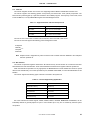
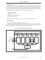
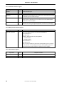
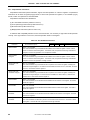
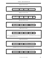
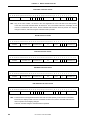
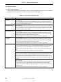
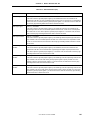
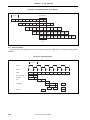
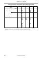
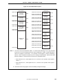
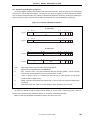
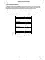
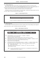
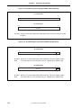
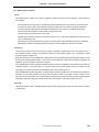
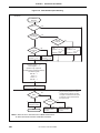
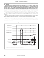
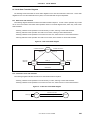
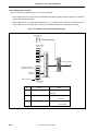
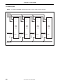
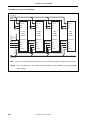
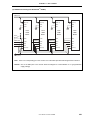
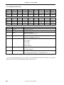
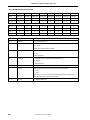
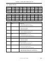
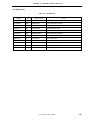
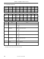
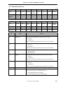
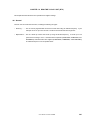
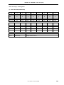
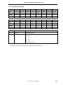
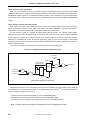
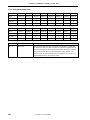
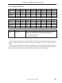
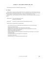
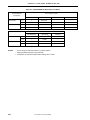
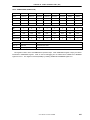
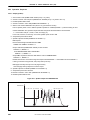
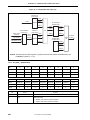
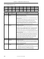
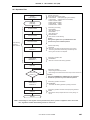
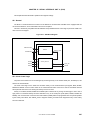
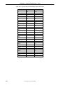
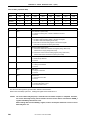
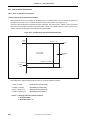
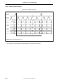
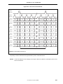
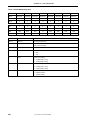
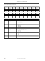
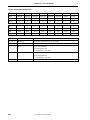
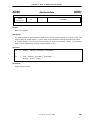
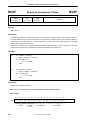
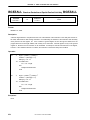
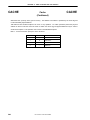
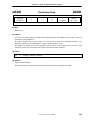
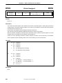
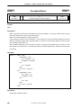
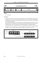
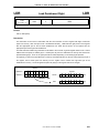
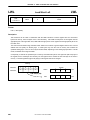
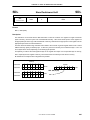
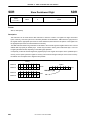
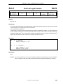
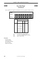
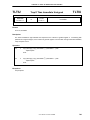
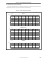
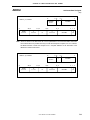
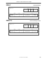
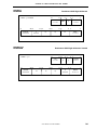
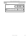
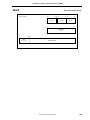
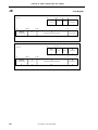
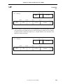
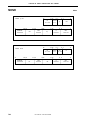
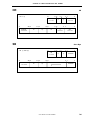
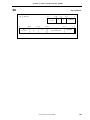
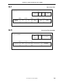
CHAPTER 6 MEMORY MANAGEMENT SYSTEM
6.4 System Control Coprocessor
The System Control Coprocessor (CP0) is implemented as an integral part of the CPU, and supports memory
management, address translation, exception handling, and other privileged operations.
The CP0 contains the
registers and a 32-entry TLB shown in Figure 6-9. The sections that follow describe how the processor uses each of
the memory management-related registers.
Remark
Each CP0 register has a unique number that identifies it; this number is referred to as the register
number. See Chapter 1 for details. Also see Chapter 7 for the CP0 functions and the relationships
between exception processing and registers.
Figure 6-9. CP0 Registers and the TLB
Used for memory management
EntryLo0
2*
EntryHi
10*
EntryLo1
3*
Used for exception processing
Index
0*
Context
4*
BadVAddr
8*
Random
1*
Count
9*
Compare
11*
PageMask
5*
Status
12*
Cause
13*
Wired
6*
EPC
14*
WatchLo
18*
PRId
15*
WatchHi
19*
XContext
20*
Config
16*
Parity Error
26*
Cache Error
27*
31
TLB
(Safe entries)
(See Random register for
TLB Wired boundary.)
0 127/255
LLAddr
17*
0
TagLo
28*
TagHi
29*
ErrorEPC
30*
Remark *: Register number
Caution
When accessing the CP0 register, some instructions require consideration of the interval time
until the next instruction is executed, because it takes a while from when the contents of the
CP0 register change to when this change is reflected on the CPU operation. This time lag is
called CP0 hazard. For details, see Chapter 29.
146
User’s Manual U14272EJ1V0UM00