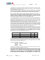
1
Technical
Information
Manual
Revision n. 11
22 February 2010
MOD. V1290 A/N
VX1290 A/N
NPO:
00104/03:V1X90.MUTx/11
32/16 CHANNEL
MULTIHIT TDCs
MANUAL REV.11
CAEN will repair or replace any product within the guarantee period if the Guarantor declares
that the product is defective due to workmanship or materials and has not been caused by
mishandling, negligence on behalf of the User, accident or any abnormal conditions or
operations.
CAEN declines all responsibility for damages or
injuries caused by an improper use of the Modules due
to negligence on behalf of the User. It is strongly
recommended to read thoroughly the CAEN User's
Manual before any kind of operation.
This product must be installed by qualified personnel; in order to be CE
compliant it requires 3-phase EMC filter type EPCOS B84143-A16-R105
on the mains supply cable; this filter does not support operation in
hostile areas (magnetic field).
CAEN reserves the right to change partially or entirely the contents of this Manual at any time
and without giving any notice.
Disposal of the Product
The product must never be dumped in the Municipal Waste. Please check your local
regulations for disposal of electronics products.
Document type:
User's Manual (MUT)
Title:
Mod. V1290-VX1290 A/N, 32/16 Ch. Multihit TDC
Revision date:
22/02/2010
Revision:
11
TABLE OF CONTENTS
1.
2.
GENERAL DESCRIPTION.......................................................................................................................10
1.1.
OVERVIEW .............................................................................................................................................10
1.2.
BLOCK DIAGRAM ...................................................................................................................................11
FUNCTIONAL DESCRIPTION................................................................................................................12
2.1. HPTDC OVERVIEW ................................................................................................................................12
2.1.1.
TDC chips architecture .................................................................................................................12
2.1.1.1.
Very High Resolution Mode ..................................................................................................................... 14
2.2.
OPERATING MODE SELECTION ................................................................................................................15
2.3.
CONTINUOUS STORAGE MODE ...............................................................................................................16
2.4. TRIGGER MATCHING MODE ...................................................................................................................16
2.4.1.
Timing constraints .........................................................................................................................19
2.5.
3.
INTEGRAL-NON-LINEARITY COMPENSATION ..........................................................................................20
TECHNICAL SPECIFICATIONS ............................................................................................................23
3.1.
PACKAGING ............................................................................................................................................23
3.2.
POWER REQUIREMENTS ..........................................................................................................................23
3.3.
FRONT PANEL.........................................................................................................................................24
3.4. EXTERNAL CONNECTORS ........................................................................................................................25
3.4.1.
INPUT connectors .........................................................................................................................25
3.4.2.
CONTROL connector ....................................................................................................................25
3.4.3.
EXTERNAL TRIGGER connectors................................................................................................26
3.5. OTHER FRONT PANEL COMPONENTS .......................................................................................................27
3.5.1.
Displays .........................................................................................................................................27
3.6. INTERNAL HARDWARE COMPONENTS .....................................................................................................27
3.6.1.
Switches .........................................................................................................................................27
3.7.
4.
TECHNICAL SPECIFICATIONS TABLE .......................................................................................................29
OPERATING MODES ...............................................................................................................................30
4.1.
INSTALLATION........................................................................................................................................30
4.2.
POWER ON SEQUENCE ...........................................................................................................................30
4.3.
POWER ON STATUS ................................................................................................................................31
4.4. ADDRESSING CAPABILITY.......................................................................................................................31
4.4.1.
Addressing via Base Address.........................................................................................................32
4.4.2.
Base addressing examples .............................................................................................................33
4.4.3.
MCST/CBLT addressing................................................................................................................33
4.4.4.
MCST/CBLT addressing examples ................................................................................................35
4.5. INTERRUPTER CAPABILITY .....................................................................................................................36
4.5.1.
Interrupt Status/ID.........................................................................................................................36
NPO:
00104/03:V1X90.MUTx/11
Filename:
V1290_REV11.DOC
Number of pages:
96
Page:
3
Document type:
User's Manual (MUT)
4.5.2.
4.5.3.
4.5.4.
Title:
Mod. V1290-VX1290 A/N, 32/16 Ch. Multihit TDC
Revision date:
22/02/2010
Revision:
11
Interrupt Level ...............................................................................................................................36
Interrupt Generation......................................................................................................................36
Interrupt Request Release..............................................................................................................36
4.6. TRIGGER MATCHING MODE DATA TRANSFER.........................................................................................37
4.6.1.
D32 OUTPUT BUFFER readout (Trigger Matching) .................................................................37
4.6.2.
BLT32/64 OUTPUT BUFFER readout with Bus Error and Event Aligned BLT disabled............37
4.6.3.
BLT32/64 OUTPUT BUFFER readout with Bus Error enabled ...................................................38
4.6.4.
BLT32/64 OUTPUT BUFFER readout with Event Aligned BLT enabled.....................................39
4.6.5.
BLT32/64 OUTPUT BUFFER readout with both Event Aligned BLT and Bus Error enabled.....40
4.6.6.
CBLT32/64 OUTPUT BUFFER readout.......................................................................................40
4.6.7.
D32 and BLT32/MBLT readout with Event FIFO enabled ...........................................................41
4.7. COUNTINUOUS STORAGE MODE DATA TRANSFER ..................................................................................42
4.7.1.
D32 OUTPUT BUFFER readout (Continuous Storage) ..............................................................42
4.7.2.
BLT32/64 OUTPUT BUFFER readout (Continuous Storage) ......................................................43
4.8. RESET LOGIC ..........................................................................................................................................43
4.8.1.
Software and Hardware CLEAR ...................................................................................................43
4.8.2.
Software RESET ............................................................................................................................44
4.8.3.
Hardware RESET ..........................................................................................................................44
4.8.4.
Software Event Count RESET........................................................................................................44
4.8.5.
Hardware Bunch Count RESET ....................................................................................................44
4.9.
5.
FIRMWARE UPGRADE..............................................................................................................................45
OPERATING CODES ................................................................................................................................46
5.1.
PROGRAMMING CAPABILITY ...................................................................................................................46
5.2. ACQUISITION MODE OPCODES ................................................................................................................49
5.2.1.
Set Trigger Matching Mode (CODE 00xx)....................................................................................49
5.2.2.
Set Continuous Storage Mode (CODE 01xx).................................................................................49
5.2.3.
Read acquisition mode (CODE 02xx)............................................................................................49
5.2.4.
Set keep_token (CODE 03xx) ........................................................................................................50
5.2.5.
Clear keep_token (CODE 04xx) ....................................................................................................50
5.2.6.
Load default configuration (CODE 05xx) .....................................................................................50
5.2.7.
Save User configuration (CODE 06xx) .........................................................................................50
5.2.8.
Load User configuration (CODE 07xx).........................................................................................50
5.2.9.
Set auto load User configuration (CODE 08xx)............................................................................51
5.2.10. Set auto load default configuration (CODE 09xx) ........................................................................51
5.3. TRIGGER OPCODES ..............................................................................................................................51
5.3.1.
Set window width (CODE 10xx) ....................................................................................................51
5.3.2.
Set window offset (CODE 11xx) ....................................................................................................51
5.3.3.
Set extra search margin (CODE 12xx) ..........................................................................................52
5.3.4.
Set reject margin (CODE 13xx).....................................................................................................52
5.3.5.
Enable subtraction of trigger time (CODE 14xx).........................................................................52
5.3.6.
Disable subtraction of trigger time (CODE 15xx).........................................................................52
5.3.7.
Read trigger configuration (CODE 16xx) .....................................................................................52
5.4. TDC EDGE DETECTION AND RESOLUTION OPCODES ............................................................................52
5.4.1.
Set edge detection configuration (CODE 22xx).............................................................................53
5.4.2.
Read edge detection configuration (CODE 23xx) .........................................................................53
5.4.3.
Set LSB of leading/trailing edge (CODE 24xx) .............................................................................53
5.4.4.
Set leading time and width resolution when pair10 (CODE 25xx) .................................................53
5.4.5.
Read resolution (CODE 26xx).......................................................................................................54
5.4.6.
Set channel dead time between hits (CODE 28xx) ........................................................................55
5.4.7.
Read channel dead time between hits (CODE 29xx) .....................................................................55
NPO:
00104/03:V1X90.MUTx/11
Filename:
V1290_REV11.DOC
Number of pages:
96
Page:
4
Document type:
User's Manual (MUT)
Title:
Mod. V1290-VX1290 A/N, 32/16 Ch. Multihit TDC
Revision date:
22/02/2010
Revision:
11
5.5. TDC READOUT OPCODES ....................................................................................................................56
5.5.1.
Enable TDC Header and Trailer in readout (CODE 30xx)...........................................................56
5.5.2.
Disable TDC Header and Trailer in readout (CODE 31xx) .........................................................56
5.5.3.
Read TDC Header and Trailer status (CODE 32xx)....................................................................56
5.5.4.
Set maximum number of hits per event (CODE 33xx) ...................................................................56
5.5.5.
Read maximum number of hits per event (CODE 34xx)................................................................57
5.5.6.
Enable TDC error mark (CODE 35xx)..........................................................................................57
5.5.7.
Disable TDC error mark (CODE 36xx) ........................................................................................57
5.5.8.
Enable bypass TDC if error (CODE 37xx)....................................................................................57
5.5.9.
Disable bypass TDC if error (CODE 38xx)...................................................................................57
5.5.10. Enable TDC internal error type (CODE 39xx)..............................................................................57
5.5.11. Read enabled TDC internal error type (CODE 3Axx)..................................................................58
5.5.12. Set effective size of readout FIFO (CODE3Bxx) ...........................................................................58
5.5.13. Read effective size of readout FIFO (CODE3Cxx)........................................................................58
5.6. CHANNEL ENABLE OPCODES ...............................................................................................................59
5.6.1.
Enable channel nn (CODE 40nn)..................................................................................................59
5.6.2.
Disable channel nn (CODE 41nn).................................................................................................59
5.6.3.
Enable all channels (CODE 42xx).................................................................................................59
5.6.4.
Disable all channels (CODE 43xx) ...............................................................................................59
5.6.5.
Write enable pattern (CODE 44xx) ...............................................................................................59
5.6.6.
Read enable pattern (CODE 45xx)................................................................................................60
5.6.7.
Write enable pattern 32 (CODE 460n)..........................................................................................60
5.6.8.
Read enable pattern 32 (CODE 470n) ..........................................................................................61
5.7. ADJUST OPCODES................................................................................................................................61
5.7.1.
Set global offset (CODE 50xx) ......................................................................................................61
5.7.2.
Read global offset (CODE 51xx) ...................................................................................................61
5.7.3.
Set channel nn adjust (CODE 52nn)..............................................................................................62
5.7.4.
Read channel nn adjust (CODE 53nn) ..........................................................................................62
5.7.5.
Set RC adjust of TDC n (CODE 540n) ..........................................................................................62
5.7.6.
Read RC adjust of TDC n (CODE 550n).......................................................................................62
5.7.7.
Save RC adjust on EEPROM (CODE 56xx) ..................................................................................63
5.8. MISCELLANEOUS ....................................................................................................................................63
5.8.1.
Read ID code of TDC n (CODE 600n) ..........................................................................................63
5.8.2.
Read firmaware rev. of microcontroller (CODE 61xx) .................................................................63
5.8.3.
Reset PLL and DLL (CODE 62xx) ................................................................................................63
5.9. ADVANCED ............................................................................................................................................64
5.9.1.
Write word nn into the Scan Path Setup (CODE 70nn).................................................................64
5.9.2.
Read word nn into the Scan Path Setup (CODE 71nn) .................................................................64
5.9.3.
Load the Scan Path Setup (CODE 72xx) .......................................................................................64
5.9.4.
Reload the default Scan Path Setup (CODE 73xx)........................................................................64
5.9.5.
Read errors in the TDC n status (CODE 740n)............................................................................64
5.9.6.
Read the DLL LOCK bit of the TDC n (CODE 750n) ...................................................................65
5.9.7.
Read the TDC n status (CODE 760n)...........................................................................................65
5.9.8.
Load the Scan Path Setup in the TDC n (CODE 770n) ................................................................65
5.10.
TEST AND DEBUG ...............................................................................................................................65
5.10.1. Write EEPROM (CODE C0xx)......................................................................................................65
5.10.2. Read EEPROM (CODE C1xx) ......................................................................................................66
5.10.3. Revision and Date Microcontroller firmware (CODE C2xx) ........................................................66
5.10.4. Write Spare (CODE C3xx) ............................................................................................................66
5.10.5. Read Spare (CODE C4xx) .............................................................................................................66
5.10.6. Enable Test Mode (CODE C5xx) ..................................................................................................66
5.10.7. Disable Test Mode (CODE C6xx) .................................................................................................67
5.10.8. Set TDC Test output (CODE C7xn)...............................................................................................67
NPO:
00104/03:V1X90.MUTx/11
Filename:
V1290_REV11.DOC
Number of pages:
96
Page:
5
Document type:
User's Manual (MUT)
Title:
Mod. V1290-VX1290 A/N, 32/16 Ch. Multihit TDC
Revision date:
22/02/2010
Revision:
11
5.10.9. Set DLL Clock (CODE C8xx) ........................................................................................................67
5.10.10.
Read TDC Setup Scan Path (CODE C9xn) ...............................................................................67
6.
VME INTERFACE .....................................................................................................................................68
6.1. REGISTER ADDRESS MAP ........................................................................................................................68
6.1.1.
Configuration ROM.......................................................................................................................69
6.2. OUTPUT BUFFER REGISTER ....................................................................................................................70
6.2.1.
Trigger Matching Mode.................................................................................................................70
6.2.1.1.
6.2.2.
6.2.3.
TDC Measurement ................................................................................................................................... 72
Continuous Storage Mode .............................................................................................................72
Filler ..............................................................................................................................................72
6.3.
CONTROL REGISTER ...............................................................................................................................73
6.4.
STATUS REGISTER ..................................................................................................................................75
6.5.
ADER 32 REGISTER (ONLY FOR VX1290 A/N)......................................................................................76
6.6.
ADER 24 REGISTER (ONLY FOR VX1290 A/N)......................................................................................77
6.7.
ENABLE ADER REGISTER (ONLY FOR VX1290 A/N) ..............................................................................77
6.8.
INTERRUPT LEVEL REGISTER .................................................................................................................77
6.9.
INTERRUPT VECTOR REGISTER...............................................................................................................78
6.10.
GEO ADDRESS REGISTER ..................................................................................................................78
6.11.
MCST BASE ADDRESS REGISTER ......................................................................................................78
6.12.
MCST/CBLT CONTROL REGISTER ....................................................................................................79
6.13.
MODULE RESET REGISTER .................................................................................................................79
6.14.
SOFTWARE CLEAR REGISTER .............................................................................................................79
6.15.
SOFTWARE EVENT RESET REGISTER ..................................................................................................79
6.16.
SOFTWARE TRIGGER REGISTER ..........................................................................................................80
6.17.
EVENT COUNTER REGISTER ...............................................................................................................80
6.18.
EVENT STORED REGISTER ..................................................................................................................80
6.19.
ALMOST FULL LEVEL REGISTER ........................................................................................................80
6.20.
BLT EVENT NUMBER REGISTER ........................................................................................................81
6.21.
FIRMWARE REVISION REGISTER .........................................................................................................81
6.22.
TESTREG REGISTER ............................................................................................................................81
6.23.
OUT_PROG CONTROL REGISTER .....................................................................................................82
6.24.
MICRO REGISTER ...............................................................................................................................82
6.25.
MICRO HANDSHAKE REGISTER ..........................................................................................................82
6.26.
DUMMY32 REGISTER .........................................................................................................................83
6.27.
DUMMY16 REGISTER .........................................................................................................................83
6.28.
SELECT FLASH REGISTER ...................................................................................................................83
6.29.
FLASH MEMORY.................................................................................................................................83
NPO:
00104/03:V1X90.MUTx/11
Filename:
V1290_REV11.DOC
Number of pages:
96
Page:
6
Document type:
User's Manual (MUT)
Title:
Mod. V1290-VX1290 A/N, 32/16 Ch. Multihit TDC
Revision date:
22/02/2010
Revision:
11
6.30.
COMPENSATION SRAM PAGE REGISTER .............................................................................................83
6.31.
EVENT FIFO.......................................................................................................................................84
6.32.
EVENT FIFO STORED REGISTER.........................................................................................................84
6.33.
EVENT FIFO STATUS REGISTER .........................................................................................................84
6.34.
COMPENSATION SRAM .......................................................................................................................85
APPENDIX A: FLASH MEMORY ACCESSES .............................................................................................86
APPENDIX B: OPERATION IN LOWER RESOLUTION MODES............................................................91
APPENDIX C: DEFAULT SET UP SCAN PATH...........................................................................................92
REFERENCES ....................................................................................................................................................96
LIST OF FIGURES
FIG. 1.1: MOD. V1290A BLOCK DIAGRAM ............................................................................................................11
FIG. 2.1: TDC SIMPLIFIED BLOCK DIAGRAM .........................................................................................................12
FIG. 2.2: PULSE DETECTION ....................................................................................................................................13
FIG. 2.3: R-C DELAY LINES IN VERY HIGH RESOLUTION MODE ..............................................................................15
FIG. 2.4: CONTINUOUS STORAGE ............................................................................................................................16
FIG. 2.5: MOD. V1290A/N TRIGGER MATCHING MODE TIMING DIAGRAM ............................................................17
FIG. 2.6: TRIGGER MATCHING WINDOWS OVERLAP ................................................................................................18
FIG. 2.7: STORAGE OF HITS OCCURRED PRIOR TRIGGERING ....................................................................................19
FIG. 2.8: STORAGE OF HITS WHICH MAY OCCUR AFTER TRIGGERING ......................................................................19
FIG. 2.9 INL I/O CHARACTERISTIC ........................................................................................................................20
FIG. 2.10 INL TRACE @ 100PS ...............................................................................................................................21
FIG. 2.11 RMS EXAMPLE AFTER INL COMPENSATION............................................................................................21
FIG. 2.12 INL AFTER COMPENSATION.....................................................................................................................22
FIG. 3.1: MODEL V1290 A/V1290 N FRONT PANELS ..............................................................................................24
FIG. 3.2: CONTROL CONNECTOR PIN ASSIGNMENT ..............................................................................................26
FIG. 3.3: COMPONENT LOCATION (V1290 A).........................................................................................................28
FIG. 4.1: BASE ADDRESSING: EXAMPLE 1 ..............................................................................................................33
FIG. 4.2: MCST/CBLT ADDRESSING EXAMPLE .....................................................................................................35
FIG. 4.3 EXAMPLE OF BLT DATA TRANSFER WITH BERR AND EVENT ALIGNED BLT DISABLED...........................38
FIG. 4.4 EXAMPLE OF BLT DATA CYCLE WITH BERR ENABLED AND EVENT ALIGNED BLT DISABLED .................38
FIG. 4.5 EXAMPLE OF BLT DATA CYCLE WITH BERR DISABLED AND EVENT ALIGNED BLT ENABLED .................39
FIG. 4.6 EXAMPLE OF BLT DATA TRANSFER WITH BERR AND EVENT ALIGNED BLT ENABLED ...........................40
FIG. 4.7 MEB READOUT WITH EVENT FIFO ENABLED...........................................................................................42
FIG. 5.1: MICRO REGISTER .....................................................................................................................................46
NPO:
00104/03:V1X90.MUTx/11
Filename:
V1290_REV11.DOC
Number of pages:
96
Page:
7
Document type:
User's Manual (MUT)
Title:
Mod. V1290-VX1290 A/N, 32/16 Ch. Multihit TDC
Revision date:
22/02/2010
Revision:
11
FIG. 5.2: OUTPUT BUFFER: THE TEST WORD ...........................................................................................................67
FIG. 6.1: OUTPUT BUFFER: THE GLOBAL HEADER..................................................................................................70
FIG. 6.2: OUTPUT BUFFER: THE TDC HEADER .......................................................................................................71
FIG. 6.3: OUTPUT BUFFER: THE TDC MEASUREMENT ............................................................................................71
FIG. 6.4: OUTPUT BUFFER: THE TDC TRAILER .......................................................................................................71
FIG. 6.5: OUTPUT BUFFER: THE TDC ERROR .........................................................................................................71
FIG. 6.6: OUTPUT BUFFER: THE EXTENDED TRIGGER TIME TAG ............................................................................71
FIG. 6.7: OUTPUT BUFFER: THE TRAILER ...............................................................................................................72
FIG. 6.8: OUTPUT BUFFER: THE FILLER ..................................................................................................................72
FIG. 6.9: CONTROL REGISTER.................................................................................................................................73
FIG. 6.10: STATUS REGISTER ..................................................................................................................................75
FIG. 6.11: ADER 32 REGISTER...............................................................................................................................76
FIG. 6.12: ADER 24 REGISTER...............................................................................................................................77
FIG. 6.13: ENABLE ADER REGISTER .....................................................................................................................77
FIG. 6.14: INTERRUPT LEVEL REGISTER .................................................................................................................77
FIG. 6.15: INTERRUPT VECTOR REGISTER ..............................................................................................................78
FIG. 6.16: GEOGRAPHICAL ADDRESS REGISTER ......................................................................................................78
FIG. 6.17: MCST/CBLT ADDRESS REGISTER .........................................................................................................79
FIG. 6.18: MCST/CBLT CONTROL REGISTER ........................................................................................................79
FIG. 6.19: TRIGGER COUNTER REGISTER................................................................................................................80
FIG. 6.20: EVENT STORED REGISTER ......................................................................................................................80
FIG. 6.21: ALMOST FULL LEVEL REGISTER ............................................................................................................80
FIG. 6.22: BLT EVENT NUMBER REGISTER ............................................................................................................81
FIG. 6.23 FIRMWARE REVISION REGISTER .............................................................................................................81
FIG. 6.24: TESTREG REGISTER ................................................................................................................................81
FIG. 6.25: OUT_PROG REGISTER ............................................................................................................................82
FIG. 6.26: MICRO REGISTER ...................................................................................................................................82
FIG. 6.27: MICRO HANDSHAKE REGISTER ..............................................................................................................82
FIG. 6.28: SELECT FLASH REGISTER .......................................................................................................................83
FIG. 6.29: COMPENSATION SRAM PAGE REGISTER .................................................................................................84
FIG. 6.30: EVENT FIFO REGISTER ..........................................................................................................................84
FIG. 6.31: EVENT FIFO STORED REGISTER .............................................................................................................84
FIG. 6.32: EVENT FIFO STATUS REGISTER .............................................................................................................85
FIG. 6.33: COMPENSATION SRAM ARCHITECTURE (V1290 A) ........................................................................85
FIG. A.1: FLASH ARCHITECTURE (V1290 A)........................................................................................................86
FIG. B.1: LOWER RESOLUTION MODES DATA FORMAT ............................................................................................91
NPO:
00104/03:V1X90.MUTx/11
Filename:
V1290_REV11.DOC
Number of pages:
96
Page:
8
Document type:
User's Manual (MUT)
Title:
Mod. V1290-VX1290 A/N, 32/16 Ch. Multihit TDC
Revision date:
22/02/2010
Revision:
11
LIST OF TABLES
TABLE 3.1: MODEL V1290 A/N POWER REQUIREMENTS ........................................................................................23
TABLE 3.2 : MODEL V1290 A/N TECHNICAL SPECIFICATIONS................................................................................29
TABLE 4.1: MODULE RECOGNISED ADDRESS MODIFIER.........................................................................................32
TABLE 4.2: CLEAR/RESET EFFECT ON THE MODEL V1290A/N REGISTERS.........................................................45
TABLE 5.1: OPERATING CODES LIST .......................................................................................................................47
TABLE 6.1: ADDRESS MAP FOR THE MODEL V1290A/N........................................................................................68
TABLE 6.2: ROM ADDRESS MAP FOR THE MODEL V1290A/N ..............................................................................69
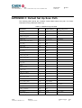
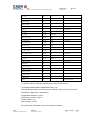
TABLE C.1: DEFAULT SET UP SCAN PATH .............................................................................................................92
NPO:
00104/03:V1X90.MUTx/11
Filename:
V1290_REV11.DOC
Number of pages:
96
Page:
9
Document type:
User's Manual (MUT)
Title:
Mod. V1290-VX1290 A/N, 32/16 Ch. Multihit TDC
Revision date:
22/02/2010
Revision:
11
1. General description
1.1. Overview
The Model V1290 A is a 1-unit wide VME 6U module that houses 32 independent
Multi-Hit/Multi-Event Time to Digital Conversion channels. The unit houses 4 High
Performance TDC chips, developed by CERN/ECP-MIC Division. Resolution is 25 ps (21
bit dynamics). The module accepts both ECL and LVDS inputs.
The Model V1290 N is a 1-unit wide VME 6U module that houses 16 independent
Multi-Hit/Multi-Event Time to Digital Conversion channels. The unit houses 2 High
Performance TDC chips and shares most of its features with the V1290 A. The module
accepts NIM inputs.
The VX1290 A and the VX1290 N are the VME64X mechanics versions of the Mod.
V1290 A and of the Mod. V1290 N respectively. They provide all the features of the std.
VME versions, moreover they support the GEOgraphical Address.
The CERN/ECP-MIC HPTDC is a General Purpose time-to-digital converter, with 32
channels per chip. The chips can be enabled to the detection of the rising and/or falling
edges.
The data acquisition can be programmed in "EVENTS" (“TRIGGER MATCHING MODE”
with a programmable time window: the so called match window) or in "CONTINUOUS
STORAGE MODE".
The board houses a 32 kwords deep Output Buffer, that can be readout via VME (as
single data, Block Transfer and Chained Block Transfer) in a completely independent
way from the acquisition itself.
The TDCs’ programming is performed via a microcontroller that implements a high-level
interface towards the User in order to mask the TDCs' hardware.
Both the Mod. V1290 A and the Mod. V1290 N fit into standard, V430 and VME64x
VMEbus crates.
The Mod. VX1290 A and the Mod. VX1290 N require VME64x VMEbus crates.
The unit accepts the following CONTROL signals (ECL differential, 110 Ω) in common to
all channels:
TRG: a common TRIGGER input;
CRST: allows the TDCs’ Bunch Count Reset (see § 4.8.5)1;
CLK: allows to provide an external Clock to the board;
CLR: erases data from the Output Buffer and performs TDCs global reset;
L2A/L2R: Level 2 Accept/Reject (2nd level trigger, not yet implemented);
AUX: auxiliary input (not yet implemented).
1
Refer also to [4] J. Christiansen, “HPTDC Version 2.1”, for details
NPO:
00104/03:V1X90.MUTx/11
Filename:
V1290_REV11.DOC
Number of pages:
96
Page:
10
Document type:
User's Manual (MUT)
Title:
Mod. V1290-VX1290 A/N, 32/16 Ch. Multihit TDC
Revision date:
22/02/2010
Revision:
11
The TRIGGER can be also sent as NIM signal on a double (bridged) LEMO00 connector.
An ECL output, OUT_PROG, whose function can be programmed (see § 6.23), is also
available on the CONTROL Bus.
Six front panel LEDs show the status of the unit:
- DTACK lights up each time the module generates the VME signal DTACK;
- PWR lights up when the module is correctly supplied
- TERM ON lights up when all the lines of the CONTROL bus are terminated;
- FULL lights up when the memory is full;
- ERROR lights up when a global error in the TDCs occurs;
- DATA READY lights up when the Event/Data Ready condition occurs (see § 6.4).
The module houses a VME INTERRUPTER [2]: the interrupt is generated as soon as the
buffer is almost full (programmable).
The module works in A24/A32 mode.
The internal registers are available in D16 or D32 mode, while the data buffer is available
in D32, BLT32 or MBLT64. The module supports also the Chained Block Transfer
mechanism (CBLT) and the Multicast commands (MCST), see § 4 for the module’s
addressing and data transfer details.
N.B.: in the present manual the “generic” term “V1290” refers to all versions;
“V1290 A” refers to both V1290 A and VX1290 A; “V1290 N” refers to both V1290 N
and VX1290 N; except as otherwise specified.
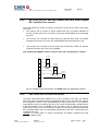
1.2. Block Diagram
FRONT PANEL
FLASH
AT45DB041B
4Mb
SRAM
IDT71V016
64Kx16
INL Compensation Table
SI SO SCK
µC
ATMEG
A16
JTAG
ACEX EP1K100
HITs
ECL/LVDS to
LVDS
Translators
CONTROL
ECL to TTL
Translators
TDCs
TDCs
TDCs
TDCs
32
Readout
Controller
32
VME
Interface
FIFO
IDT72V3690
32Kx32
VME BUS
8
VME TRANSCEIVERs
16
32
Fig. 1.1: Mod. V1290A Block Diagram
The function of each block will be explained in detail in the following sections.
NPO:
00104/03:V1X90.MUTx/11
Filename:
V1290_REV11.DOC
Number of pages:
96
Page:
11
Document type:
User's Manual (MUT)
Title:
Mod. V1290-VX1290 A/N, 32/16 Ch. Multihit TDC
Revision date:
22/02/2010
Revision:
11
2. Functional description
2.1. HPTDC overview
The V1290A/N modules are based on High Performance TDC chips, developed by
CERN/ECP-MIC Division [4].
In order to achieve a better use of the module, an overview of the TDC chips operation
will be shown in the following sections.
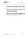
2.1.1.
TDC chips architecture
DLL
Coarse Counter
Clock
PLL
X4
Hit[31:0]
Hit register 0
Hit register 1
Hit
cont.
Hit register 2
Hit register 3
X8
L1 Buffer
Trigger
Interface
Trigger
Fifo
256
Readout
Fifo
- Programming
- Status
16
Trigger
Matching
control
Trigger
Matching
JTAG
Trigger
256
Readout
Interface
32
Tokin
Tokout
Fig. 2.1: TDC Simplified Block Diagram
The time base for the TDC measurements is a Delay Locked Loop (DLL) with 32 delay
elements and a clock synchronous counter (coarse counter), both driven from the same
clock reference. The clock reference can be taken directly from the clock input of the
TDC chip (40 MHz) or can come from an on-chip PLL; the PLL can be used as a filter to
NPO:
00104/03:V1X90.MUTx/11
Filename:
V1290_REV11.DOC
Number of pages:
96
Page:
12
Document type:
User's Manual (MUT)
Title:
Mod. V1290-VX1290 A/N, 32/16 Ch. Multihit TDC
Revision date:
22/02/2010
Revision:
11
remove jitter on the input clock (40 MHz) or can perform clock multiplication (160/320
MHz) to increase time resolution:
40 MHz (clock input or clock filtered) and DLL with 32 delay elements → 781 ps (800 ps)
160 MHz and DLL with 32 delay elements → 195 ps (200 ps)
320 MHz and DLL with 32 delay elements → 98 ps (100 ps)
A hit measurement is performed by storing the state of the DLL (fine/vernier counter) and
the coarse counter in one hit register when a hit is detected. The TDC can be
programmed to detect individual leading and/or trailing edges of the hit signal, or
alternatively to perform a paired measurement consisting of one leading edge and the
corresponding pulse width.
leading
trailing
leading and trailing
paired
Fig. 2.2: Pulse detection
Each channel can store 4 hit measurements before being written into a 256 words deep
buffer (L1 buffer) shared by a group of 8 channels.
The hit registers content is written into the L1 buffer together with a channel identifier. A 8
bit channel dependant offset programmable is added to the measurement before writing
it into the L1 buffer.
If the channel buffer is full, when a new hit arrives, it will be ignored.
The two operation modes will be described in detail in the relevant sections; at this point
we must remember that, when the module works in Continuous Storage mode (see
§ 2.3), measurements stored in the L1 buffer are passed directly to a common Readout
FIFO.
When the module works in Trigger Matching mode (see § 2.4) a trigger matching function
selects hits related to a trigger. The trigger information, consisting of a trigger time tag
(bunch id) and an event id, are stored temporarily in a 16 words deep Trigger FIFO. A
time window of programmable size is available for the trigger matching to accommodate
the time spread of hits related to the same event.
The read-out FIFO is 256 words deep and its main function is to enable data to be read
out while others are being processed. The effective size of the readout FIFO can be
“artificially” reduced via the programming.
The TDCs feature several readout interfaces (parallel, serial, via Jtag, byte wise).
The V1290 features a parallel readout with the FPGA like read-out controller and all
TDCs in the chain configured as slaves. The master sends the token (Tokin in Fig. 2.1) to
the first slave chip in the chain which then starts to send its data. The read-out of
individual words are controlled by a Data_ready / Get_data handshake. The token
(Tokout in Fig. 2.1) is then passed on to the following slave TDCs in the chain until it
finally arrives at the master.
NPO:
00104/03:V1X90.MUTx/11
Filename:
V1290_REV11.DOC
Number of pages:
96
Page:
13
Document type:
User's Manual (MUT)
Title:
Mod. V1290-VX1290 A/N, 32/16 Ch. Multihit TDC
Revision date:
22/02/2010
Revision:
11
In continuous storage a slave TDC can be programmed to keep token until no more data;
otherwise the TDC passes the token (after one datum has been transferred); in trigger
matching mode each slave must be programmed in order to keep the token until the end
of the event.
It is possible to configure the programmable features in the TDC via JTAG, and also to
get access to test facilities built into the TDC.
Programming of the device is separated into two scan path groups: setup scan path and
control scan path.
The JTAG setup scan path is used to load programming data that can not be changed
while the TDC is actively running. The JTAG setup scan path consists of a 646 bit
configuration sequence plus one parity bit; refer to [4], page 32 for a detailed description.
The JTAG control scan path is used to enable/disable channels which can be done while
the TDC is actively running. The JTAG control scan path is also used to initialize the PLL
and DLL after power up: it consists of a 38 bit configuration sequence plus one parity bit;
refer to [4], page 39 for a detailed description.
The setup/control scan paths have a parity bit which is continuously monitored for
potential parity errors caused by single event upsets. Any detected parity error will set the
respective error bit in the JTAG status register. Via JTAG it is possible to get access to
the status of the TDC at any time. to monitor the TDC error status and all internal buffers
occupancies (refer to [4], page 40).
On V1290 TDC programming and status monitoring is performed by an on board
microcontroller (see § 5).
The HPTDC features 3 types of reset (refer to [4], page 16):
Event count reset: loads the programmed event count offset into the event id counter
(useful in Trigger Matching mode only);
Bunch count reset: loads the programmed offsets into the coarse time counter, the trigger
time tag (bunch id) counter and the reject counter; pratically, it represents the T0 time
reference.
Global reset: clears all buffers in the TDC, initialises all internal state machines and
counters to their initial state and clears all detected error conditions.
See § 4.8 for details about the V1290A/N reset logic.
2.1.1.1.
Very High Resolution Mode
When the PLL is used to perform the clock multiplication up to 320 MHz and the DLL is
configured with 32 delay elements, the resolution is 100 ps, as described in the previous
section.
The time resolution can be improved furtherly, by performing multiple sampling of the
DLL signals, controlled from a precisely calibrated delay line.
On HPTDC this interpolation within a DLL cell is obtained by sampling the DLL signals
four times, equally spaced over the interval of a delay cell (using four cascaded TDC
channels in order to obtain one very high resolution channel). The sampling signals must
be generated with very small delays (25 ps) and high precision and stability. This is done
using a R-C delay line having very small dependencies on temperature and supply
voltage.
Both the R-C delay line adjustment and the DLL compensation are obtained via proper
default settings.
NPO:
00104/03:V1X90.MUTx/11
Filename:
V1290_REV11.DOC
Number of pages:
96
Page:
14
Document type:
User's Manual (MUT)
Title:
Mod. V1290-VX1290 A/N, 32/16 Ch. Multihit TDC
Revision date:
22/02/2010
Revision:
11
Fig. 2.3: R-C delay lines in Very High resolution mode
The time measurements from the four normal channels can still be considered as
individual time measurements; an on-chip interpolation can be performed over such
measurements in order to compress them into one single very high resolution time
measurement, thus obtaining a TDC chip with 8 very high resolution channels (estimated
resolution: 25 ps circa).
In very high resolution R-C mode the TDC can be programmed to detect individual
leading and/or trailing edges but the paired measurement is not available.
Because of the process variations of the R-C delay line, a calibration of its parameters is
required. The calibration constants per chip are limited to 4 x 3 bits used to control the
four sampling taps from the R-C delay line (see § 5.7.5 and § 5.7.6).
For the R-C delay line calibration a statistical code density test can be found. A code
density test consists of histogramming the occurrence of each interpolation point over a
set of random hits. This histogram (for a sufficiently large population of random hits) is a
direct measure of the time span of each tap of the RC delay chain. A flat histogram is the
ideal case where all time taps have equal size and covers uniformly the delay of one
delay cell in the DLL.
Also integral non-linearities in the DLL can be compensated for by small adjustable
delays on each signal tap from the DLL. For applications where a very precise integral
linearity is required these can be used to compensate for mismatches in the delay line of
the DLL.
2.2. Operating mode selection
Two different module setups are selectable via software for different acquisition
scenarios, namely:
NPO:
00104/03:V1X90.MUTx/11
Filename:
V1290_REV11.DOC
Number of pages:
96
Page:
15
Document type:
User's Manual (MUT)
Title:
Mod. V1290-VX1290 A/N, 32/16 Ch. Multihit TDC
−
Continuous Storage Mode
−
Trigger Matching Mode
Revision date:
22/02/2010
Revision:
11
It is possible to switch from one operation setup to the other by simply reprogramming:
the operating mode can be selected via the 00xx and 01xx OPCODES (see § 5.2).
N.B: with this operation the data in memory will be lost.
See § 6.2 for a full description of the data format.
2.3. Continuous Storage Mode
In this readout mode the data loaded into the L1 Buffer are straightly forwarded into the
Readout FIFO of the TDC, where they are readout (by the FPGA master) and then
loaded in the Output Buffer. All the hits received by the enabled channels are stored as
valid data into the Output Buffer. The Time Origin (Time Zero) is represented by the
latest RESET (see § 3.4.2).
0
1
2
3
4 5
HIT ch[0..127]
Reset
Fig. 2.4: Continuous storage
The storage of data in the Output Buffer never foresees the writing of the control words
(HEADER and TRAILER). The data are written in sequential order2, reflecting the time
evolution of the external signals:
DATUM #1HIT time(1)
DATUM #2HIT time(2)
DATUM #3HIT time(3)
DATUM #4HIT time(4)
DATUM #5HIT time(5)
DATUM #6HIT time(6)
If the total rate of HIT signals is higher than the transfer rate of the data from the TDCs to
the Output Buffer (or from the Output Buffer to the VME) an overflow condition will be
met:
OVERFLOW:
− Error word written into the FIFO
− Status register FULL bit set
In this case there will be a data loss.
2.4. Trigger Matching Mode
Trigger matching is performed as a time match between a trigger time tag and the
channel time measurements themselves. The trigger time tag is taken from the trigger
2
Hits closer than 25 ns might actually be misplaced.
NPO:
00104/03:V1X90.MUTx/11
Filename:
V1290_REV11.DOC
Number of pages:
96
Page:
16
Document type:
User's Manual (MUT)
Title:
Mod. V1290-VX1290 A/N, 32/16 Ch. Multihit TDC
Revision date:
22/02/2010
Revision:
11
FIFO and the time measurements are taken from the L1 buffer. Hits matching a trigger
are passed to the common TDC readout FIFO.
A match between a trigger and a hit is detected within a programmable time window.
The trigger matching control on the V1290 is handled through 4 programmable
3
parameters (see § 5.3.1 and § 5.3.4):
−
−
−
−
match window,
window offset,
extra search margin,
reject margin.
reject latency
reject
margin
(programmable)
match window width (programmable)
extra search
margin
(programmable)
trigger input
window offset (programmable)
search window
t
Fig. 2.5: Mod. V1290A/N Trigger Matching Mode timing diagram
The trigger is defined as the bunch ID when the event of interest occurred. The trigger
matching being based on the bunch ID means that the “resolution” of the trigger matching
is one clock cycle (25 ns) and the configuration parameters of the trigger matching mode
are also specified in steps of clock cycles.
The window offset is the temporal distance (with sign, see Fig. 2.5 and Fig. 2.7) between
the trigger and the start of the trigger matching window. A specific requirement of the
trigger matching function implemented in the HPTDC is that the trigger must be
subsequent to the match window. This is required to insure that all hits matching a trigger
are already in the L1 buffer when a trigger matching search is started.
On the V1290 it is possible also to program a match window straddling the trigger or
subsequently to the trigger (see § 2.4.1): this is possible because an artificial delay (40
clock cycle = 1 µs ) is induced on the trigger.
The search for hits matching a trigger is performed within an extended search window to
guarantee that all matching hits are found even when the hits have not been written into
the L1 buffer in strict temporal order. For normal applications it is sufficient to make the
search window eight clock cycles larger than the match window (default setting for the
V1290).
To prevent buffer overflows and to speed up the search time an automatic reject function
reject older hits, when no triggers are waiting in the trigger FIFO. A separate reject
counter runs with a programmable offset to detect hits to reject. The reject margin should
be set to be at least 1 clock cycle to insure that no hits of interest are rejected.
3
The parameters programmable on the V1290 are functions of other 4 parameters which define
the trigger matching function implemented in the HPTDC. The microcontroller translates the
parameters set by the User on the V1290 into the parameters required by the chips.
NPO:
00104/03:V1X90.MUTx/11
Filename:
V1290_REV11.DOC
Number of pages:
96
Page:
17
Document type:
User's Manual (MUT)
Title:
Mod. V1290-VX1290 A/N, 32/16 Ch. Multihit TDC
Revision date:
22/02/2010
Revision:
11
In trigger matching mode all data belonging to an event are written into the common
read-out FIFO between a TDC Header and a TDC Trailer. The TDC Header contains an
event id and a bunch id (trigger time tag) and the TDC Trailer contains the same event id
plus the event word count.
The stored data can represent an absolute time measurement (where time 0 is the latest
reset) or optionally all time measurements read out are referenced to the start of match
window (see § 5.3.5 and 5.3.6).
The trigger matching can be programmed to match a defined maximum number of hits to
each trigger. The hits assigned to an event is in this case done on a “first come first
served” basis. If the limiting function has rejected hits this will be signalled via an error
marking word in the end of the event.
In case an error condition (L1 buffer overflow, Trigger FIFO overflow, memory parity
error, limiting number of hits matched to event, etc.) has been detected during the trigger
matching a special word with error flags is generated.
A unique feature of the trigger matching in the HPTDC is its capability to assign hit
measurements to multiple triggers.
1
2
3
4
5
6
7
8
hits
9
overlap
window N+1
window N
trig N
trig N+1
Fig. 2.6: Trigger matching windows overlap
If the Fig 2.5 shows hits received by one TDC, the events have the following structure:
TDC header, event id N, trigger time tag N (if enabled)
DATUM Hit time 2
DATUM Hit time 3
DATUM Hit time 4
DATUM Hit time 5
DATUM Hit time 6
TDC trailer, event id N, number data 5 (if enabled)
TDC header, event id N+1, trigger time tag N+1 (if enabled)
DATUM Hit time 5
DATUM Hit time 6
DATUM Hit time 7
DATUM Hit time 8
TDC trailer, event id N+1, number data 4 (if enabled)
If Overflow occurs, the Global Trailer Full Bit is set to one.
NPO:
00104/03:V1X90.MUTx/11
Filename:
V1290_REV11.DOC
Number of pages:
96
Page:
18
Document type:
User's Manual (MUT)
Title:
Mod. V1290-VX1290 A/N, 32/16 Ch. Multihit TDC
2.4.1.
Revision date:
22/02/2010
Revision:
11
Timing constraints
The trigger matching related parameters must be programmed according to the following
constraints.
1st case: the trigger matching window precedes the trigger arrival:
Match window (programmed)
hit
hit hit
hit hit
Trigger
Window offset <0 (programmed)
Fig. 2.7: Storage of hits occurred prior triggering
The window width and the window offset are encoded on 12 bit (25 ns LSB):
Match window width < |window offset| ≤ 4095 clock cycle = 102375 ns
Note that in this case the window offset is negative.
2nd case: the trigger matching window is “straddling” the trigger or delayed with
respect to the trigger:
Match window (programmed)
hit
hit hit
hit hit
Trigger
window offset <0
(programmed)
hit
Trigger
hit hit
hit hit
window offset >0
(programmed)
Fig. 2.8: Storage of hits which may occur after triggering
As previously described, the HPTDC does not allow to program a trigger matching
window straddling the trigger or delayed with respect to the trigger; anyway this is
allowed in the V1290, by providing a 1 µs (40 clock cycles) delay on the trigger; the
allowed trigger matching windows must thus agree with the following constraint:
Match window width + window offset ≤ 40 clock cycles = 1000 ns
Note that in this case the Window offset can be either negative or positive, see Fig. 2.8.
NPO:
00104/03:V1X90.MUTx/11
Filename:
V1290_REV11.DOC
Number of pages:
96
Page:
19
Document type:
User's Manual (MUT)
Title:
Mod. V1290-VX1290 A/N, 32/16 Ch. Multihit TDC
Revision date:
22/02/2010
Revision:
11
2.5. Integral-non-linearity Compensation
The INL represents the error of the Input-Output characteristic t-D of the TDC with
respect to the ideal one which is given by the following function:
D(t) = int (t / LSB)
ideal characteristic
Where D is the output data, t is the input time, LSB is the bin size (25ps) and int(x)
represents the integer part of x.
NOTE: with analog circuit based TDCs, there is a variation of the LSB size due to the
variation of gain and offset of the analog parts; in this case, the ideal input-output
characteristic is given by the best-fit line calculated on the real input-output curve of the
TDC (the best fit line is that one which minimizes the RMS error); the INL is then
calculated as the difference between the curve and the best fit line. In the case of digital
TDC (like the V1290), the gain and the offset come from a clock and it is very precise, so
the ideal line can be calculated a priori without any interpolation (gain = 1/LSB, offset =
0). It must be noticed that the TDC chips feature an intrinsic INL, due to DNL, which has
a 25 ns period ( = TCLOCK).
DATA
6
5
INL(3)
4
INL(2)
3
2
1
BIN(0)
BIN(1)
BIN(2)
BIN(3)
BIN(4)
BIN(5)
time
INL
Fig. 2.9 INL I/O Characteristic
NPO:
00104/03:V1X90.MUTx/11
Filename:
V1290_REV11.DOC
Number of pages:
96
Page:
20
Document type:
User's Manual (MUT)
Title:
Mod. V1290-VX1290 A/N, 32/16 Ch. Multihit TDC
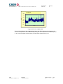
V1290A
V890 -INL
INL
Revision date:
22/02/2010
Revision:
11
25ps
20,00
LSB
15,00
10,00
5,00
0,00
-5,00
0
512
1024
Fig. 2.10 INL trace @ 100ps
The INL curve can be corrected using a compensation look-up table: the curve is periodic
so the LUT will cover only the BINs in a clock period . A sample which falls in a certain
BIN inside the clock period is corrected by the subtraction of the INL value for that BIN.
LSB = 25ps:
LUT[n] = round(INL[n]) n=[0:1023]
D’ = D - LUT[D & 0x3FF]
NOTE: after the compensation, some missing codes can appear on the histogram; in
fact, all the BINs are “scrambled” by the LUT and it is possible that BIN[x] is moved into
BIN[y] but no BIN[z] is moved into BIN[x] which remains empty.
Std Dev @ 25ps (σ=1.09 / RMS=27ps)
34
26
34
30
34
34
34
38
34
42
34
46
34
50
34
54
34
58
34
62
34
66
34
70
34
74
80000
70000
60000
50000
40000
30000
20000
10000
0
Fig. 2.11 RMS example after INL compensation
NPO:
00104/03:V1X90.MUTx/11
Filename:
V1290_REV11.DOC
Number of pages:
96
Page:
21
Document type:
User's Manual (MUT)
Title:
Mod. V1290-VX1290 A/N, 32/16 Ch. Multihit TDC
V1290AV890
INL
Revision date:
22/02/2010
Revision:
11
- INL 25ps
4,00
3,00
LSB
2,00
1,00
0,00
-1,00
-2,00
0
512
1024
Fig. 2.12 INL after compensation
The Lock-Up table was calculated and loaded into the Flash Memory (see Appendix A).
The INL compensation can be disabled by setting to 0 the compensation enable bit (bit 5)
in the Control Register (default setting: compensation enabled, see § 6.3).
NPO:
00104/03:V1X90.MUTx/11
Filename:
V1290_REV11.DOC
Number of pages:
96
Page:
22
Document type:
User's Manual (MUT)
Title:
Mod. V1290-VX1290 A/N, 32/16 Ch. Multihit TDC
Revision date:
22/02/2010
Revision:
11
3. Technical specifications
3.1. Packaging
The modules are housed in a 6U-high, 1U-wide VME unit. The boards host the VME P1,
and P2 connectors and fit into both VME standard and V430 backplanes.
3.2. Power requirements
The power requirements of the modules’ versions are as follows:
Table 3.1: Model V1290 A/N power requirements
NPO:
00104/03:V1X90.MUTx/11
Power supply
Mod. V1290A
Mod. V1290N
+5 V
2.80 A
1.50 A
Filename:
V1290_REV11.DOC
Number of pages:
96
Page:
23
Document type:
User's Manual (MUT)
Title:
Mod. V1290-VX1290 A/N, 32/16 Ch. Multihit TDC
Revision date:
22/02/2010
Revision:
11
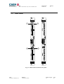
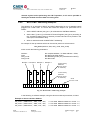
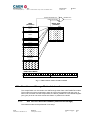
3.3. Front Panel
Mod.
V560E
Mod.
V560E
Mod. V1290A
Mod. V1290N
DTACK
-
DTACK
+
15
14
31
13
I
N
P
U
T
I
N
P
U
T
12
11
10
9
16
8
PWR
PWR
TERM
TERM
FULL
FULL
C
O
N
T
R
O
L
C
O
N
T
R
O
L
AUX
POUT
L2R
L2A
CLK
CLR
TRG
CRST
-
+
-
ERROR
+
ERROR
DRDY
DRDY
TRIGGER
TRIGGER
-
AUX
POUT
L2R
L2A
CLK
CLR
TRG
CRST
+
7
15
6
5
I
N
P
U
T
I
N
P
U
T
4
3
2
1
0
SCALE
R
32 CH
25 PS
MULTIHIT TDC
016
CH
SCALE
R
16 CH
25 PS
MULTIHIT TDC
Fig. 3.1: Model V1290 A/V1290 N front panels
NPO:
00104/03:V1X90.MUTx/11
Filename:
V1290_REV11.DOC
Number of pages:
96
Page:
24
Document type:
User's Manual (MUT)
Title:
Mod. V1290-VX1290 A/N, 32/16 Ch. Multihit TDC
Revision date:
22/02/2010
Revision:
11
3.4. External connectors
The location of the connectors is shown in Fig. 3.1.Their function and electro-mechanical
specifications are listed in the following subsections.
3.4.1.
INPUT connectors
Mod. V1290 A:
Mechanical specifications:
two 17+17-pin, 3M 3431-5202 Header-type connectors.
Electrical specifications:
ECL/LVDS input signals (see front panel for input polarity), 110 Ω impedance. The 17th
higher pair of pins of each connector is ground connected.
LOWER BLOCK INPUT:
input signals from channel 0 through channel 15.
HIGHER BLOCK INPUT:
input signals from channel 16 through channel 31.
Mod. V1290 N:
Mechanical specifications:
16 LEMO 00 connectors.
Electrical specifications:
NIM input signals, 50 Ω impedance.
LOWER BLOCK INPUT:
input signals from channel 0 through channel 7.
HIGHER BLOCK INPUT:
input signals from channel 8 through channel 15.
3.4.2.
CONTROL connector
Mechanical specifications:
two 8+8-pin, 3M 3408-5202 Header-type connectors.
-
AUX: not used.
OUT_PROG: differential ECL level, 110 Ω impedance.
L2_REJECT: not used.
L2_ACCEPT: not used.
CLOCK: Rising-edge active, differential ECL level, 110 Ω; 40 MHz max freq.
CLR: Active high, differential ECL level, 110 Ω impedance; min. width 25 ns.
TRIGGER: Rising-edge active, differential ECL level, 110 Ω; min. width 25 ns, double
Trigger resolution: 75 ns.
CRST: Rising-edge active, differential ECL level, 110 Ω; min. width 25 ns.
Pin assignment is shown in Fig. 3.2.
NPO:
00104/03:V1X90.MUTx/11
Filename:
V1290_REV11.DOC
Number of pages:
96
Page:
25
Document type:
User's Manual (MUT)
Title:
Mod. V1290-VX1290 A/N, 32/16 Ch. Multihit TDC
Revision date:
22/02/2010
Revision:
11
/AUX
AUX
/OUT_PROG
OUT_PROG
/L2_REJ
L2_REJ
/L2_A
L2_A
/CLK
CLK
/CLR
CLR
/TRG
3
TRG
/CRST
CRST
2
1
Fig. 3.2: CONTROL connector pin assignment
3.4.3.
EXTERNAL TRIGGER connectors
Mechanical specifications:
two 00-type LEMO connectors (bridged).
Electrical specifications:
Rising-edge active, NIM, high impedance; min. width 25 ns, double Trigger resolution:
75 ns
If this input is used, a 50 Ohm termination is required; in daisy chain configuration, the
termination must be inserted on the last board in the chain.
This signal is internally or-wired with the TRG signal on the Control Connector (see
§ 3.4.2)
NPO:
00104/03:V1X90.MUTx/11
Filename:
V1290_REV11.DOC
Number of pages:
96
Page:
26
Document type:
User's Manual (MUT)
Title:
Mod. V1290-VX1290 A/N, 32/16 Ch. Multihit TDC
Revision date:
22/02/2010
Revision:
11
3.5. Other front panel components
3.5.1.
Displays
The front panel (refer to Fig. 3.1) hosts the following LEDs:
DTACK:
Colour: green.
Function: it lights up green whenever a VME read/write
access to the board is performed.
PWR:
Colour: green/red.
Function: it lights up green when the board is inserted into the
crate and the crate is powered up; when it is red, it indicates
that there is an over-current status: in this case, remove the
overload source, switch the module off and then switch it on
again.
TERM:
Colour: green.
Function: it lights up green when the lines of the control bus
are terminated.
FULL:
Colour: red.
Function: it lights up when the Output Buffer is full.
ERROR:
Colour: red.
Function: it lights up to signal a TDC global error
DRDY:
Colour: yellow.
Function: it lights up when at least one event/data (depending
on acquisition mode, see § 6.4) is present in the Output
Buffer.
N.B.: FULL, ERROR and DRDY LEDs light up for a while at power ON to indicate
that the board is configuring.
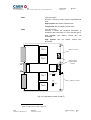
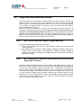
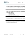
3.6. Internal hardware components
The V1290 A module is constituted by a motherboard with 2 piggy-back boards plugged
into it. The V1290 N has the input connectors on a piggy-back board. In the following
some hardware setting components, located on the boards, are listed. See Fig. 3.5 for
their exact location on the PCB and their settings.
3.6.1.
Switches
ROTARY SWITCHES:
NPO:
00104/03:V1X90.MUTx/11
Filename:
V1290_REV11.DOC
Type: 4 rotary switches.
Function: they allow to select the VME address of the
module. See Fig. 3.3 for their location.
Number of pages:
96
Page:
27
Document type:
User's Manual (MUT)
Title:
Mod. V1290-VX1290 A/N, 32/16 Ch. Multihit TDC
Revision date:
22/02/2010
Revision:
11
Type: DIP switch.
Function: it allows to switch from/to internal/external
clock
SW1:
Right position (dot visible): external clock;
Left position (dot not visible): internal clock.
Type: DIP switch.
Function: it allows the hardware termination (if
enabled) of the Control Bus on 110 Ω (see also § 6.3)
SW2:
Low position
terminated;
(dot
visible):
High position
terminated.
(dot
not
TDC3
Control
visible):
Bus
not
Control
Bus
VME P1 connector
TDC2
Rotary switches
for Base address
selection
BKP
J13
STD
SW1
TDC1
CLK
INT
CLK
EXT
TERM
ON
TDC0
VME P2 connector
SW2
TERM
OFF
Fig. 3.3: Component Location (V1290 A4)
4
Mod. V1290 N has two TDC chips only
NPO:
00104/03:V1X90.MUTx/11
Filename:
V1290_REV11.DOC
Number of pages:
96
Page:
28
Document type:
User's Manual (MUT)
Title:
Mod. V1290-VX1290 A/N, 32/16 Ch. Multihit TDC
Revision date:
22/02/2010
Revision:
11
3.7. Technical specifications table
Table 3.2 : Model V1290 A/N technical specifications
6U-high, 1U-wide VME unit
Refer to Table 3.1
V1290 A: 32 ECL / LVDS inputs, 110 Ω impedance
V1290 N: 16 NIM inputs, 50 Ω impedance
5 ns
Trigger Matching Mode; Continuous Storage Mode
Programmable (see § 5.3)
32 kwords deep Output Buffer
25 ps
52 µs
Packaging
Power requirements
Inputs
Double hit resolution
Acquisition modes
Match window
Built-in memory
LSB
Dynamic Range
RMS resolution
(with compensation5 enabled)
Integral non linearity
5
(with compensation enabled)
Max. differential non linearity
(with compensation5 disabled)
Interchannel Isolation
Offset spread
EXT TRIGGER input
Double Trigger resolution
Clock source
Control inputs
Control outputs
Displays
VME
35 ps (typical)
<2.5 LSB
<3 LSB
≤3 LSB
6
<2 ns
Two LEMO 00 bridged connectors, NIM signal, 50 Ω
75 ns
Internal (40 MHz) or External (on Control connector), dip switch
selectable
active-high, differential ECL input signals:
CLR: performs the Hardware CLEAR (min. width: 25 ns), see § 4.8.1
rising-edge active, differential ECL input signals:
CRST: performs the Bunch RESET (min. width: 25 ns), see § 4.8.5
CLK: external clock (max. freq.: 40 MHz)
TRG: trigger for the TDC latching (min. width: 25 ns)
differential ECL output signal:
OUT_PROG: control output signal, programmable via the
out prog control register (see § 6.23)
DTACK: green LED; lights up at each VME access.
PWR: green/red LED; green: power ON, red: failure status.
TERM: green LED; control bus termination ON.
FULL: red LED; memory full.
ERROR: red LED; TDC global error.
DRDY: yellow LED; at least one datum/event in the Output Buffer
Addressing modes: A24, A32, MCST
Data transfer modes: D16, D32, MBLT32, BLT64, CBLT32, CBLT64
Readout rate: 33 Mbyte/s
5
See § 2.5
6
It can be compensated via Offset Adjust, see § 5.7
NPO:
00104/03:V1X90.MUTx/11
Filename:
V1290_REV11.DOC
Number of pages:
96
Page:
29
Document type:
User's Manual (MUT)
Title:
Mod. V1290-VX1290 A/N, 32/16 Ch. Multihit TDC
Revision date:
22/02/2010
Revision:
11
4. Operating modes
4.1. Installation
The Mod. V1290A/N boards fit into both V430 VME 6U (JAUX dataway) and standard 6U
VME crates. Refer to § 1.1 for details on the various versions. The boards support live
insertion/extraction into/from the crate, i.e. it is possible to insert or extract them from the
crate without turning the crate off.
CAUTION: all cables connected to the front panel of the board must be removed
before extracting/inserting the board from/into the crate.
CAUTION
ALL CABLES MUST BE REMOVED FROM THE FRONT PANEL
BEFORE EXTRACTING THE BOARD FROM THE CRATE!
4.2. Power ON sequence
To power ON the board follow this procedure:
1. insert the V1290A/N board into the crate: as the board is inserted, the PWR
green LED (see § 3.5.1) lights up indicating that the board is powered;
2. after insertion, the TERM LED lights up green (if the TERM switch is ON), the
FULL LED and the ERROR LED become red and the DRDY LED becomes
yellow; this indicates that the board is turned on and is configuring;
3. after a few seconds, the FULL, the ERROR and the DRDY LEDs will light off: this
indicates that the board is ready to acquire data.
N.B.: if the PWR LED becomes red instead of being green, there is an overload and
the over-current protection is now running. In order to acquire data, it is necessary
to remove the overload source, then turn the board off and switch it on again.
Sometimes, it may happen that the PWR LED is red as soon as the board is
inserted in the crate: this is due to the fact that the board has been just misplaced
into the crate. In this case, extract the board and insert it again into the crate.
NPO:
00104/03:V1X90.MUTx/11
Filename:
V1290_REV11.DOC
Number of pages:
96
Page:
30
Document type:
User's Manual (MUT)
Title:
Mod. V1290-VX1290 A/N, 32/16 Ch. Multihit TDC
Revision date:
22/02/2010
Revision:
11
4.3. Power ON status
At power ON the module is in the following status:
•
the Output Buffer is cleared;
•
registers are set to their default configuration (see § 5 and § 6);
•
the TDCs are in the following status (see also § 5):
trigger matching
disabled
matching window width
500 ns (0x14)
matching window offset
-1 µs (0xFFD8)
extra search window
200 ns (0x8)
reject margin
100 ns (0x4)
keep token
set
subtraction trigger time
disabled
global offset
0
channel offset
0 (all channel)
edge detection
leading
trailing/leading resolution
25 ps
TDC header/Trailer
enabled
error mark
enabled
error bypass
disabled
error type
all enabled
dead time between hits
5 ns
TDC readout FIFO size
256
max number of hits per event
no limit
channels
all enabled
At power ON or after a hardware reset the module must thus be set to the desired
configuration.
4.4. Addressing capability
The module can be addressed in 2 different ways, specifically:
1. via Base Address;
2. via Multicast/Chained Block Transfer addressing mode.
NPO:
00104/03:V1X90.MUTx/11
Filename:
V1290_REV11.DOC
Number of pages:
96
Page:
31
Document type:
User's Manual (MUT)
4.4.1.
Title:
Mod. V1290-VX1290 A/N, 32/16 Ch. Multihit TDC
Revision date:
22/02/2010
Revision:
11
Addressing via Base Address
The module works in A24/A32 mode. This implies that the module’s address must be
specified in a word of 24 or 32 bit. The Address Modifier codes recognised by the module
are summarised in Table 4.1.
Table 4.1: Module recognised Address Modifier
A.M.
0x3F
0x3E
0x3D
0x3C
0x3B
0x3A
0x39
0x38
0x0F
0x0E
0x0D
0x0C
0x0B
0x0A
0x09
0x08
Description
A24 supervisory block transfer
A24 supervisory program access
A24 supervisory data access
A24 supervisory 64 bit block transfer
A24 non privileged block transfer
A24 non privileged program access
A24 non privileged User data access
A24 non privileged 64 bit block transfer
A32 supervisory block transfer
A32 supervisory program access
A32 supervisory data access
A32 supervisory 64 bit block transfer)
A32 non privileged block transfer
A32 non privileged program access
A32 non privileged data access
A32 non privileged 64 bit block transfer
The Base Address can be selected in the range:
0x000000
0x00000000
ÅÆ
ÅÆ
0xFF0000
0xFFFF0000
A24 mode
A32 mode
The Base Address of the module can be fixed through four rotary switches, housed on
two piggy-back boards plugged into the main printed circuit board (see § 3.6.1)
NPO:
00104/03:V1X90.MUTx/11
Filename:
V1290_REV11.DOC
Number of pages:
96
Page:
32
Document type:
User's Manual (MUT)
Title:
Mod. V1290-VX1290 A/N, 32/16 Ch. Multihit TDC
4.4.2.
Revision date:
22/02/2010
Revision:
11
Base addressing examples
The following is an example of Base Addressing for two boards inserted in a VME crate.
BOARD 1
BOARD 2
Upper Rotary
Switches
(Lower bytes
of Address)
00
11
Lower Rotary
Switches
(Upper bytes
of Address)
EE
1
2
3
4
5
6
Slots
in the crate
CC
7
8
9 10 11 12 13 14 15 16 17 18 19 20 21
Fig. 4.1: Base Addressing: Example 1
If the board 1 and board 2 are respectively with the rotary switches for VME Base
Addressing set as shown in the figure, the complete address of the registers of the two
boards will be as follows:
Board 1:
Base addressing A32:
Base addressing A24:
0xEE000000 + offset
0x000000 + offset
Board 2:
Base addressing A32:
Base addressing A24:
0xCC110000 + offset
0x110000 + offset
4.4.3.
MCST/CBLT addressing
When the Multicast/Chained Block Transfer addressing mode is adopted, the module
works in A32 mode only. The Address Modifiers codes recognised by the module are:
MCST:
CBLT:
NPO:
00104/03:V1X90.MUTx/11
0x0E
0x0D
0x0A
0x09
0x0F
0x0C
0x0B
0x08
A32 supervisory block transfer
A32 supervisory 64 bit block transfer
A32 non privileged block transfer
A32 non privileged 64 bit block transfer
A32 supervisory block transfer
A32 supervisory 64 bit block transfer
A32 non privileged block transfer
A32 non privileged 64 bit block transfer
Filename:
V1290_REV11.DOC
Number of pages:
96
Page:
33
Document type:
User's Manual (MUT)
Title:
Mod. V1290-VX1290 A/N, 32/16 Ch. Multihit TDC
Revision date:
22/02/2010
Revision:
11
The boards can be accessed in Multicast Commands mode (MCST mode, see [2]), that
allows to write in the registers of several boards at the same time by accessing the
MCST Base Address in A32 only once.
The boards can be accessed in Chained Block Transfer mode (CBLT mode, see [2]) that
allows to readout sequentially a certain number of contiguous boards in a VME crate.
This access is allowed in BLT32 and BLT64 modes only to the MCST Base Address.
N.B.: The Base Address used for MCST and CBLT operations is the same, i.e.
throughout this User's Manual the "MCST Base Address" identifies the same
Address, used both for MCST commands (in Write only, for the allowed registers)
and the CBLT Readout (in Read only, for the Output Buffer only).
The MCST Base Address must be set in a different way from the ordinary Base Address.
Its most significant byte (i.e. bits 31 through 24 of base address) must be written in the
MCST/CBLT Address Register (see § 6.11) and must be set in common to all boards
belonging to the MCST/CBLT chain (i.e. all boards must have the same setting of the
MCST/CBLT Base Address on bits 31 through 24). The default setting is 0xAA.
In CBLT/ MCST operations, the IACKIN/ IACKOUT daisy chain is used to pass a token
from one board to the following one. The board which has received the token
stores/sends the data from/to the master via MCST / CBLT access. No empty slots must
thus be left between the boards or, in alternative, empty slots can be left only in case
VME crates with automatic IACKIN/IACKOUT short-circuiting are used.
Once the addresses have been set, the first and last board in a chain must have,
respectively, only the FIRST_BOARD (F_B) and only the LAST_BOARD (L_B) bit set to
1 in the MCST Control Register (see § 6.12). On the contrary, all intermediate boards
must have both the FIRST_BOARD and the LAST_BOARD bits set to 1 (active,
intermediate) or both the FIRST_BOARD and the LAST_BOARD bits set to 0 (inactive).
By default these bits are set to 0 (the board is inactive).
Board status
Board position in the chain
F_B bit
L_B bit
inactive
active
active
active
last
first
intermediate
0
0
1
1
0
1
0
1
Please note that in a chain there must be one (and only one) first board (i.e. a board with
F_B bit set to 1 and the L_B bit set to 0) and one (and only one) last board (i.e. a board
with F_B bit set to 0 and the L_B bit set to 1).
The complete address in A32 mode is:
A [31:24]
A [23:16]
A [15:0]
MCST/CBLT Address
00
offset
In MCST/CBLT operation it is possible to define more chains in the same crate, but each
chain must have an address different from the other.
N.B.: In CBLT operation the data coming from different boards are tagged with the
HEADER and with the TRAILER words containing the GEO address in the 5 MSB
(see § 4.4.2). It is up to the User to write the GEO address in the GEO register
before executing the CBLT operation, since the V1290A/N are not enabled to pick
the GEO address from the VME Bus. If the GEO address is not written in the
NPO:
00104/03:V1X90.MUTx/11
Filename:
V1290_REV11.DOC
Number of pages:
96
Page:
34
Document type:
User's Manual (MUT)
Title:
Mod. V1290-VX1290 A/N, 32/16 Ch. Multihit TDC
Revision date:
22/02/2010
Revision:
11
relevant register before performing the CBLT operation, it will not be possible to
identify the module which the data are coming from.
4.4.4.
MCST/CBLT addressing examples
The following is an example of MCST and CBLT addressing for four V1290A/N boards
plugged into a VME crate. To access the boards the steps to be performed are as
follows:
1. Set the MCST address (see § 6.11) for all boards via VME Base Address;
2. Set the bits F_B and L_B of the MCST Control Register (see § 6.12) according to
the operational status (active or inactive) of each board and to its position in the
chain (first, intermediate or last);
3. Write or read the boards via MCST/CBLT addressing.
An example of User procedures which can be used to perform a write access is:
vme_write (address, data, addr_mode, data_mode)
which contain the following parameters:
the complete address, i.e. Base Address + offset;
the data to be either written;
the addressing mode (only A32 allowed in MCST);
the data mode.
Address:
Data:
Addr_mode:
Data_mode:
BOARD 1 BOARD 2 BOARD 3 BOARD 4
1
2
3
00
11
34
71
EE
CC
BC
DD
4
5
6
7
8
Upper Rotary
Switches
(Lower bytes
of Address)
Lower Rotary
Switches
(Upper bytes
of Address)
Slots
in the crate
9 10 11 12 13 14 15 16 17 18 19 20 21
Fig. 4.2: MCST/CBLT Addressing Example
In the following, a software example, using the above mentioned procedures, is listed:
Example of Access via Base Address
vme_write (0xEE001010, 0xAA, A32, D16)
vme_write (0xCC111010, 0xAA, A32, D16)
vme_write (0xBC341010, 0xAA, A32, D16)
NPO:
00104/03:V1X90.MUTx/11
Filename:
V1290_REV11.DOC
/* set MCST Address=0xAA for board 1 */
/* set MCST Address=0xAA for board 2 */
/* set MCST Address=0xAA for board 3 */
Number of pages:
96
Page:
35
Document type:
User's Manual (MUT)
vme_write
vme_write
vme_write
vme_write
vme_write
vme_write
Title:
Mod. V1290-VX1290 A/N, 32/16 Ch. Multihit TDC
(0xDD711010,
(0xEE001012,
(0xCC111012,
(0xBC341012,
(0xDD711012,
(0xAA001014,
0xAA,
0x02,
0x03,
0x00,
0x01,
0x00,
A32,
A32,
A32,
A32,
A32,
A32,
D16)
D16)
D16)
D16)
D16)
D16)
/*
/*
/*
/*
/*
/*
Revision date:
22/02/2010
Revision:
11
set MCST Address=0xAA for board 4 */
set board 1 = First */
set board 2 = Active */
set board 3 = Inactive */
set board 4 = Last */
send SOFTWARE RESET to all the boards */
N.B.: there must be always one (and only one) FIRST BOARD and one (and only one) LAST
BOARD.
4.5. Interrupter capability
The Mod. V1290A/N house a VME INTERRUPTER. The modules respond to D16
Interrupt Acknowledge cycles providing: a word whose 8 LSB are the STATUS/ID.
4.5.1.
Interrupt Status/ID
The interrupt STATUS/ID is 8-bit wide, and it is contained in the 8 LSB of the Interrupt
Vector Register (see § 6.9). The register is available at the VME address: Base Address
+ 0x100C.
4.5.2.
Interrupt Level
The module’s interrupter produces its request on one of the 7 IRQ lines. The interrupt
level is programmable via VME (see § 6.8).
4.5.3.
Interrupt Generation
An Interrupt is generated when the number of words stored in the memory equals the
value written in the Almost Full Level Register at the VME address: Base Address
+ 0x1022 (see § 6.19). If the value in Interrupt Level Register is set to 0 the interrupt is
disabled (default setting).
4.5.4.
Interrupt Request Release
The INTERRUPTER removes its Interrupt request when either a Read Access is
performed to the Output Buffer so that the number of events stored in the memory
decreases and becomes less than the value written in the Almost Full Level Register or
when a module’s clear is performed.
NPO:
00104/03:V1X90.MUTx/11
Filename:
V1290_REV11.DOC
Number of pages:
96
Page:
36
Document type:
User's Manual (MUT)
Title:
Mod. V1290-VX1290 A/N, 32/16 Ch. Multihit TDC
Revision date:
22/02/2010
Revision:
11
4.6. Trigger Matching Mode data transfer
The Output Buffer can be readout via VME through D32, BLT32, BLT64, CBLT32 and
CBLT64 modes. The module has to be programmed in order to work in the required
mode (see § 5.2.1), and some parameters have to be set in order to keep data aligned
(i.e. to transfer an integer number of events per cycle). In the following each readout
mode will be described in detail.
Nw is the number of words which compose an event (note that such number is not
constant but changes from event to event). It’s up to the user to verify the presence of
valid data in the Output Buffer before read out; this can be performed via the Status
Register read out (Data Ready Bit, see § 6.4). When a trigger signal occurs, an event is
loaded into the Output Buffer (see § 6.2). The DATA_READY bit in the Status Register is
set to one when at least one event is present in the buffer.
4.6.1.
D32 OUTPUT BUFFER readout (Trigger Matching)
This readout mode can be performed in two ways:
•
Wait for DATA_READY bit to be set, then readout the Nw words until the global
Trailer (TRAILER).
•
Start readout without waiting for DATA_READY: if BERR is disabled, fillers will be
readout until a global header is met (otherwise, if BERR is enabled, BERR is
signalled and no filler is transferred); then Nw words will be transferred until a global
TRAILER is readout.
4.6.2.
BLT32/64 OUTPUT BUFFER readout with Bus Error and Event
Aligned BLT disabled
BLT32/64 readout with BERR and Event Aligned BLT mode disabled does not permit to
collect one or more complete events since the number of bytes Nb which are transferred
in a BLT cycle has usually a “typical” value (256, 2048…) which rarely coincide with a
multiple of the number of bytes NB composing an event, i.e. NB=Nw·4 (note that Nw is
not constant but changes from event to event). It is more than likely that in a BLT cycle
an event could be partially read out and the remaining part would be read out in the
subsequent cycle. If the Output Buffer contains a number N of words smaller than Nb/4
(the number of words readout in one BLT cycle), the module transfers its memory
content, completed with (Nb/4)-N fillers.
NPO:
00104/03:V1X90.MUTx/11
Filename:
V1290_REV11.DOC
Number of pages:
96
Page:
37
Document type:
User's Manual (MUT)
Title:
Mod. V1290-VX1290 A/N, 32/16 Ch. Multihit TDC
Revision:
11
EV
1
EV
1
EV
2
1st BLT
CYCLE
EV
2
MEB
Revision date:
22/02/2010
2nd BLT
CYCLE
EV
4
EV
4
EV
3
EV
3
3rd BLT
CYCLE
FILLER
EV
5
EV
5
Fig. 4.3 Example of BLT data transfer with BERR and Event Aligned BLT disabled
4.6.3.
BLT32/64 OUTPUT BUFFER readout with Bus Error enabled
In this mode the module produces a BERR signal (see § 6.3) once the last data in the
Output Buffer has been transferred and no filler is added.
EV
1
EV
1
EV
2
1st BLT
CYCLE
EV
2
MEB
2nd BLT
CYCLE
EV
5
EV
4
EV
4
EV
3
EV
3
EV
5
3rd BLT
CYCLE
BERR
Fig. 4.4 Example of BLT data cycle with BERR enabled and Event Aligned BLT disabled
NPO:
00104/03:V1X90.MUTx/11
Filename:
V1290_REV11.DOC
Number of pages:
96
Page:
38
Document type:
User's Manual (MUT)
4.6.4.
Title:
Mod. V1290-VX1290 A/N, 32/16 Ch. Multihit TDC
Revision date:
22/02/2010
Revision:
11
BLT32/64 OUTPUT BUFFER readout with Event Aligned BLT
enabled
This mode allows to transfer an integer number Ne of events (in fig. 4.5 Ne = 2), set via
the BLT Event Number Register (see § 6.20). The default setting value of this register is
0, so this mode disabled. In order to enable the Event Aligned BLT the desired number of
events Ne must be written in the BLT event number register. This mode allows the
module to transfer a maximum number Ne of events; three cases may occur:
•
The memory has a number of events smaller than Ne: the module transfers its
memory content (with one or more BLT cycles) and completes the cycle adding
fillers (see § 6.2.3).
•
The memory has a number of events larger than Ne and Nb/4> ΣNw 7 (where Nb/4
is the number of words transferred in one BLT cycle): the module transfers Ne
events per cycle and eventually completes the cycle adding fillers.
•
The memory has a number of events larger than Ne and Nb/4< ΣNw: the transfer
requires more than one cycle to be completed, the last cycle eventually is completed
with fillers.
EV
1
EV1
EV2
1st BLT
CYCLE
EV
2
MEB
2nd BLT
CYCLE
EV
3
EV3
EV
4
EV4
filler
3rd BLT
CYCLE
EV5
EV
5
filler
filler
Fig. 4.5 Example of BLT data cycle with BERR disabled and Event Aligned BLT enabled
7
ΣNw = total number of words
NPO:
00104/03:V1X90.MUTx/11
Filename:
V1290_REV11.DOC
Number of pages:
96
Page:
39
Document type:
User's Manual (MUT)
4.6.5.
Title:
Mod. V1290-VX1290 A/N, 32/16 Ch. Multihit TDC
Revision date:
22/02/2010
Revision:
11
BLT32/64 OUTPUT BUFFER readout with both Event Aligned
BLT and Bus Error enabled
This mode allows the module to transfer a maximum number Ne of events; three cases
may occur:
•
The memory has a number of events smaller than Ne: the module transfers its
memory content (with one or more BLT cycles) then asserts BERR, thus terminating
the cycle.
•
The memory has a number of events larger than Ne and Nb/4> ΣNw: the module
transfers Ne events in one cycle, then asserts BERR thus terminating the cycle.
•
The memory has a number of events larger than Ne and Nb/4< ΣNw: the transfer
requires more than one cycle to be completed.
N.B.: Enabling the BERR is useful in order to save time, avoiding fillers’ transfer.
EV1
EV2
EV
3
EV3
EV
4
EV4
BERR
2nd BLT
CYCLE
EV
5
BERR
3rd BLT
CYCLE
EV5
EV
1
1st BLT
CYCLE
EV
2
MEB
BERR
Fig. 4.6 Example of BLT data transfer with BERR and Event Aligned BLT enabled
4.6.6.
CBLT32/64 OUTPUT BUFFER readout
The CBLT mode allows data readout from a set of modules in the crate. The readout
starts from the first module of the set: it transfers its first event, then passes the token to
the subsequent module via the IACKIN/IACKOUT daisy chain lines. If one module’s
Output Buffer is empty or Inactive (see § 6.12), the token is passed with no data transfer.
If the data transfer is not completed by the first CBLT cycle, a second one may be
attached to the first and so on until the last module in the set has transferred its last data:
then it asserts BERR, which is automatically enabled when the CBLT is performed, thus
completing the cycle.
CBLT64: if an odd number of words is transferred, the Board completes the event
transfer by adding a filler.
NPO:
00104/03:V1X90.MUTx/11
Filename:
V1290_REV11.DOC
Number of pages:
96
Page:
40
Document type:
User's Manual (MUT)
4.6.7.
Title:
Mod. V1290-VX1290 A/N, 32/16 Ch. Multihit TDC
Revision date:
22/02/2010
Revision:
11
D32 and BLT32/MBLT readout with Event FIFO enabled
The Event FIFO has been introduced in order to help the event readout from the Output
Buffer, since the events length is unknown a priori. If the Event FIFO is enabled when an
event is written in the Output Buffer, the FPGA writes in its internal FIFO (1 kword) a 32
bit word containing the event counter on 16 bit and the event number of words (see
§ 6.18).
This allows to acknowledge the number of words that compose the event, before starting
the event readout. If the Event FIFO is enabled the events are readout in the following
way:
− Readout one (or N) word frome the Event FIFO
− Calculate Nw (or ΣNw): number of words which compose the event (or N events)
− Readout Nw (or ΣNw) in D32 and BLT32/MBLT
Note that if the Event FIFO is enabled, for each event a 32 bit word is written into the
Event FIFO: if it is never readout, then the board would become FULL after 1024 events,
although the Output Buffer would be EMPTY (all the events were readout).
The Event FIFO Status Register and the Event FIFO Stored Register allow to know how
many words are written into the Event FIFO (that, if it is correctly readout as described,
correspond to the number of events stored into the Output Buffer).
NPO:
00104/03:V1X90.MUTx/11
Filename:
V1290_REV11.DOC
Number of pages:
96
Page:
41
Document type:
User's Manual (MUT)
Title:
Mod. V1290-VX1290 A/N, 32/16 Ch. Multihit TDC
Revision date:
22/02/2010
OUTPUT BUFFER FULL
EVENT FIFO FULL
Revision:
11
BOARD FULL
EVENT FIFO
(1Kx32bit)
MEB
(32Kx32bit)
global header
EV1
0
1
2
3
NWORD0
NWORD1
NWORD2
NWORD3
1023
NWORD1023
global trailer
global header
EV2
global trailer
global header
EV3
global trailer
global header
EV4
global trailer
global header
EV1023
global trailer
EVENT FIFO WORD
31 30 29 28 27 26 25 24 23 22 21 20 19 18 17 16 15 14 13 12 11 10
EVENT COUNT
9
8
7
6
5
4
3
2
1
0
WORD COUNT
Fig. 4.7 MEB readout with Event FIFO enabled
4.7. Countinuous Storage Mode data transfer
The Output Buffer can be readout via VME through either D32 or BLT32/BLT64 modes.
The module has to be programmed in order to work in the required mode (see § 5.2.2).
When hits are written into the Output Buffer; the DATA_READY bit in the Status Register
(see § 6.4) is set to one when at least one datum is present in the buffer.
4.7.1.
D32 OUTPUT BUFFER readout (Continuous Storage)
This readout mode can be performed in two ways:
NPO:
00104/03:V1X90.MUTx/11
Filename:
V1290_REV11.DOC
Number of pages:
96
Page:
42
Document type:
User's Manual (MUT)
Title:
Mod. V1290-VX1290 A/N, 32/16 Ch. Multihit TDC
Revision date:
22/02/2010
Revision:
11
•
Set the Almost Full Level to N (see § 6.19); wait until the Almost Full bit in the Status
Register is set to one then readout the N recorded words in D32 mode.
•
Readout continuously from the buffer, removing the “fillers” via software.
•
If BERR is enabled and the Output Buffer is empty, then the board asserts BERR
without filler transfer.
4.7.2.
BLT32/64 OUTPUT BUFFER readout (Continuous Storage)
•
If BERR is disabled and the Output Buffer contains a number N of words smaller
than Nb/4 (the number of words readout in one BLT cycle, being Nb the number of
bytes per cycle), the module transfers its memory content, completed with (Nb/4)-N
fillers.
•
If BERR is enabled the module produces a BERR signal once the last data in the
Output Buffer has been transferred and no filler is added.
4.8. Reset logic
Different types of CLEAR or RESET operations are foreseen, according to the effects
they have on the module and particularly on the registers. These are:
4.8.1.
•
Software CLEAR
•
Hardware CLEAR
•
Software RESET
•
Hardware RESET
•
Software EVENT COUNT RESET
•
Hardware BUNCH COUNT RESET
Software and Hardware CLEAR
The CLEAR (whether hardware or software) clears the data off the Output Buffer, the
event counter and performs a TDCs global reset, which does not erase the TDCs
programmation. A TDC global reset in fact clears all buffers in the TDCs, initialises all
internal state machines and counters to their initial state and clears all detected error
conditions.
The CLEAR can be forwarded in several ways:
1. Via software: Software Clear Register (see § 6.14)
2. When a write access to some Registers is performed (see table 4.2)
3. When a pulse is sent to the front panel CLR input.
4. When an OPCODE (see § 5) which foresees the TDC reprogrammation is executed
The module’s registers whose content is erased by a CLEAR are listed in Table 4.2.
NPO:
00104/03:V1X90.MUTx/11
Filename:
V1290_REV11.DOC
Number of pages:
96
Page:
43
Document type:
User's Manual (MUT)
4.8.2.
Title:
Mod. V1290-VX1290 A/N, 32/16 Ch. Multihit TDC
Revision date:
22/02/2010
Revision:
11
Software RESET
The Software Reset performs the same actions of the CLEAR, moreover it resets some
other registers and initializes the TDCs to the default configuration. This type of RESET
can be forwarded by performing a write access to the Single Shot Reset Register. All the
registers reset by a Software RESET are marked in the column SR (Software Reset) in
Table 4.2.
4.8.3.
Hardware RESET
The Hardware RESET performs the same actions as the Software RESET and,
moreover, it resets some other registers. All the registers reset by a Hardware RESET
are marked in the column HR (Hardware Reset) in Table 4.2.
This kind of RESET is performed:
1. at Power ON of the module;
2. via a VME RESET (SYS_RES).
After a reset (HW or SW) the module must thus be initialised.
4.8.4.
Software Event Count RESET
The Software Event Count RESET does not perform the board’s event counter reset but
it loads the programmed event count offset into the TDCs event id counter. The Event
Counter is also reset by the hardware Clear.
4.8.5.
Hardware Bunch Count RESET
The Hardware Bunch Count RESET loads the default values (see § 5.3); it is forwarded
by sending a pulse to the CRST front panel input.
NPO:
00104/03:V1X90.MUTx/11
Filename:
V1290_REV11.DOC
Number of pages:
96
Page:
44
Document type:
User's Manual (MUT)
Title:
Mod. V1290-VX1290 A/N, 32/16 Ch. Multihit TDC
Revision date:
22/02/2010
Revision:
11
Table 4.2: CLEAR/RESET effect on the Model V1290A/N registers
Register content
Output Buffer
Control Register (*)
Status Register
Interrupt Level
Interrupt Vector
GEO Address (*)
MCST Base Address (*)
MCST/CBLT Ctrl (*)
Module Reset
Software Clear
Software Event Reset
Software Trigger
Event Counter
Event Stored
Almost Full Level (*)
BLT Event Number
Firmware Revision
Testreg
Out Prog Control
Micro (**)
Micro Handshake
Sel Flash
Flash
Compensation SRAM Page
Event FIFO
Event FIFO Stored
Event FIFO Status
Dummy 32
Dummy 16
CLR
9
SR
9
9
HR
9
9
9
9
9
9
9
9
9
9
9
9
9
9
9
9
9
9
9
9
9
9
9
9
9
9
9
9
9
9
9
9
9
9
Address
0x0000÷0x0FFC
0x1000
0x1002
0x100A
0x100C
0x100E
0x1010
0x1012
0x1014
0x1016
0x1018
0x101A
0x101C
0x1020
0x1022
0x1024
0x1026
0x1028
0x102C
0x102E
0x1030
0x1032
0x1034
0x1036
0x1038
0x103C
0x103E
0x1200
0x1204
(*) A write access to these registers causes a module’s CLEAR.
(**) See the OPCODE Table (§ 5.1)
4.9. Firmware upgrade
The board can store two firmware versions, called STD and BKP respectively; at Power
On, a microcontroller reads the Flash Memory and programs the module with the
firmware version selected via the J13 jumper (see § 3.6), which can be placed either on
the STD position, or in the BKP position. It is possible to upgrade the board firmware via
VME, by writing the Flash: for this purpose, download the software package available at:
http://www.caen.it/nuclear/product.php?mod=V1290A
The package includes the new firmware release file and a text file with C program
examples which will guide the Usert through the development of the software necessary
in order to update the Flash Memory.
N.B.: it is strongly suggested to upgrade ONLY one of the stored firmware
revisions (generally the STD one): if both revision are simoultaneously updated,
and a failure occurs, it will not be possible to upload the firmware via VME again!
NPO:
00104/03:V1X90.MUTx/11
Filename:
V1290_REV11.DOC
Number of pages:
96
Page:
45
Document type:
User's Manual (MUT)
Title:
Mod. V1290-VX1290 A/N, 32/16 Ch. Multihit TDC
Revision date:
22/02/2010
Revision:
11
5. Operating codes
5.1. Programming capability
The module programming is performed by means of an on-board microcontroller. The
User sends and receives instructions and data to/from the microcontroller via 16-bit
OPCODE setup words. The handshake is the following:
Write Operation:
− the VME (master) tests the WRITE_OK bit in the Micro Handshake Register (see
§ 6.25); if the WO bit is set to 1, the VME can write a datum;
− the WO bit is automatically reset after the datum is written and will be set back to 1
when it will be possible to write another one;
− as soon as the WO bit is set back to 1, the VME can write another datum.
Read Operation:
− a valid datum can be read via VME only if the READ_OK (RO) bit in the Micro
Handshake Register is set to 1 (see § 6.25);
− the RO bit is automatically reset after the datum is read out and will be set back to 1
when it will be possible to read another one;
− as soon as the RO bit is set back to 1, the VME can read another datum.
The OPCODE setup words have the following format:
15 14 13 12 11 10 9
COMMAND
8
7
6
5
4
3
2
1
0
OBJECT
Fig. 5.1: Micro Register
The COMMAND field specifies the operation to perform, while the OBJECT field (when
required) specifies the object over which the operation must be performed (e.g. the
channel number). If the object refers to the channel number (for example OBJ = nn in
Table 5.1), it can vary from 0 to either 1F (V1290 A) or F (V1290 N); if it refers to the
HPTDC number (OBJ = 0n in Table 5.1), it can vary from 0 to either 3 (V1290A) or 1
(V1290 N).
When the operation does not foresee an object, the OBJECT field is meaningless.
The communication with the microcontroller begins always by sending an OPCODE; if no
operands are foreseen (nR = 0 and nW = 0) the cycle ends, otherwise the microcontroller
remains in a wait status until the User has read or written all the foreseen operands.
Some opcodes imply the setup registers reprogrammation when launched and thus a
data clear, others imply the control registers reprogrammation when launched (no data
clear).
NPO:
00104/03:V1X90.MUTx/11
Filename:
V1290_REV11.DOC
Number of pages:
96
Page:
46
Document type:
User's Manual (MUT)
Title:
Mod. V1290-VX1290 A/N, 32/16 Ch. Multihit TDC
Revision date:
22/02/2010
Revision:
11
The following Table 5.1 contains, for each OPCODE, the symbolic name, the performed
operation, the number of written and read operands, the number of significant bits and
the foreseen reprogrammations.
Table 5.1: Operating codes list
COM OBJ
CODE
SYMBOLIC
OPERATION
nW
nR
nbit PR8
ACQUISITION MODE
00
-
00xx
TRG_MATCH
set trigger matching
-
-
-
s
01
-
01xx
CONT_STOR
set continuous storage
-
-
-
s
02
-
02xx
READ_ACQ_MOD
read acquisition mode
-
1
1
-
03
-
03xx
SET_KEEP_TOKEN
set keep_token
-
-
-
s
04
-
04xx
CLEAR_KEEP_TOKEN
clear keep token
-
-
-
s
05
-
05xx
LOAD_DEF_CONFIG
load default configuration
-
-
-
s
06
-
06xx
SAVE_USER_CONFIG
save User configuration
-
-
-
-
07
-
07xx
LOAD_USER_CONFIG
load User configuration
-
-
-
s
08
-
08xx
AUTOLOAD_USER_CONFIG
set auto load User configuration
-
-
-
-
09
-
09xx
AUTOLOAD_DEF_CONFIG
set auto load default configuration
-
-
-
-
TRIGGER
10
-
10xx
SET_WIN_WIDTH
set window width
1
-
12
s
11
-
11xx
SET_WIN_OFFS
set window offset
1
-
12
s
12
-
12xx
SET_SW_MARGIN
set extra search margin
1
-
12
s
13
-
13xx
SET_REJ_MARGIN
set reject margin
1
-
12
s
14
-
14xx
EN_SUB_TRG
enable subtraction of trigger time
-
-
-
s
15
-
15xx
DIS_SUB_TRG
disable subtraction of trigger time
-
-
-
s
16
-
16xx
READ_TRG_CONF
read trigger configuration
-
5
49
-
TDC EDGE DETECTION & RESOLUTION
22
-
22xx
23
-
23xx
24
-
24xx
SET_TR_LEAD_LSB
25
-
25xx
26
-
28
29
SET DETECTION9
enable leading/ trailing edge
1
-
2
s
9
read edge detection configuration
-
1
2
-
9
set LSB of leading/trailing edge
1
-
2
s
SET_PAIR_RES9
set leading time and width res. when pair
1
-
16
s
26xx
READ_RES
read resolution
-
1
16
-
-
28xx
SET_DEAD_TIME
set channel dead time between hits
1
-
2
s
-
29xx
READ_ DEAD_TIME
read channel dead time between hits
-
1
2
-
READ_DETECTION
TDC READOUT
8
These opcodes imply the TDCs reprogrammation when launched; “s” means that the setup
registers will be reprogrammed, “c” means that the control registers will be reprogrammed.
9
Some features of these Opcodes are used for test purposes in lower resolution modes: see the
relevant sections.
NPO:
00104/03:V1X90.MUTx/11
Filename:
V1290_REV11.DOC
Number of pages:
96
Page:
47
Document type:
User's Manual (MUT)
Title:
Mod. V1290-VX1290 A/N, 32/16 Ch. Multihit TDC
Revision date:
22/02/2010
Revision:
11
30
-
30xx
EN_HEAD_TRAILER
enable TDC header and TRAILER
-
-
-
s
31
-
31xx
DIS_HEAD_TRAILER
disable TDC header and TRAILER
-
-
-
s
32
-
32xx
READ_HEAD_TRAILER
read status TDC header and TRAILER
-
1
1
-
33
-
33xx
SET_EVENT_SIZE
set maximum number of hits per event
1
-
-
s
34
-
34xx
READ_EVENT_SIZE
read maximum number of hits per event
-
1
1
-
35
-
35xx
EN_ERROR_MARK
enable TDC error mark
-
-
-
s
36
-
36xx
DIS_ERROR_MARK
disable TDC error mark
-
-
-
s
37
-
37xx
EN_ERROR_BYPASS
enable bypass TDC if error
-
-
-
s
38
-
38xx
DIS_ERROR_BYPASS
disable bypass TDC if error
-
-
-
s
39
-
39xx
SET_ERROR_TYPES
set TDC internal error type
1
-
11
s
3A
-
3Axx
READ_ERROR_TYPES
read TDC internal error type
-
1
11
-
3B
-
3Bxx
SET_FIFO_SIZE
set effective size of readout FIFO
1
-
3
s
3C
-
3Cxx
READ_FIFO_SIZE
read effective size of readout FIFO
-
1
3
-
40
nn
40nn
EN_CHANNEL
enable channel nn
-
-
-
c
41
nn
41nn
DIS_CHANNEL
disable channel nn
-
-
-
c
42
-
42xx
EN_ALL_CH
enable all channels
-
-
-
c
43
-
43xx
DIS_ALL_CH
disable all channels
-
-
-
c
44
-
44xx
WRITE_EN_PATTERN
write enable pattern for channels
8
-
128
c
45
-
45xx
READ_EN_PATTERN
read enable pattern for channels
-
8
128
-
46
-
46xx
WRITE_EN_PATTERN32
write 32 bit enable pattern for channels
2
-
32
c
47
-
47xx
READ_EN_PATTERN32
read 32 bit enable pattern for channels
-
2
32
-
CHANNEL ENABLE
ADJUST
50
-
50xx
SET_GLOB_OFFS
set global offset
2
-
17
s
51
-
51xx
READ_GLOB_OFFS
read global offset
-
2
17
-
52
nn
52nn
SET_ADJUST_CH
set channel nn adjust
1
-
8
s
53
nn
53nn
READ_ADJUST_CH
read channel nn adjust
-
1
8
-
54
-
54xn
SET_RC_ADJ
Set RC adjust of tdc 0n
1
-
12
s
55
-
55xn
READ_RC_ADJ
Read RC adjust of tdc 0n
-
1
12
-
56
-
56xn
SAVE_RC_ADJ
save RC adjust on EEPROM
-
-
-
-
MISCELLANEOUS
60
0n
600n
READ_TDC_ID
read programmed ID of TDC 0n
-
2
32
-
61
-
61xx
READ_MICRO_REV
read firmware revision of microcontroller
-
1
8
-
62
-
62xx
RESET_DLL_PLL
reset DLL and PLL
-
-
-
s/c
70
nn
70nn
WRITE_SETUP_REG
write word nn into the scan path setup
1
-
16
-
71
nn
71nn
READ_SETUP_REG
read word nn into the scan path setup
-
1
16
-
72
-
72xx
UPDATE_SETUP_REG
load the scan path setup
-
-
-
s
73
-
73xx
DEFAULT_SETUP_REG
reload the default scan path setup
-
-
-
s
Number of pages:
96
Page:
48
ADVANCED
NPO:
00104/03:V1X90.MUTx/11
Filename:
V1290_REV11.DOC
Document type:
User's Manual (MUT)
Title:
Mod. V1290-VX1290 A/N, 32/16 Ch. Multihit TDC
Revision date:
22/02/2010
Revision:
11
74
0n
740n
READ_ERROR_STATUS
read errors in the TDC 0n status
-
1
11
-
75
0n
750n
READ_DLL_LOCK
read the DLL LOCK bit of the TDC 0n
-
1
1
-
76
0n
760n
READ_STATUS_STREAM
read the TDC 0n status
-
4
62
-
77
nn
77nn
UPDATE_SETUP_TDC
load the scan path setup on TDC nn
-
-
-
-
DEBUG AND TEST
C0
-
C0xx
WRITE_EEPROM
write 1 byte into the EEPROM
2
-
16
-
C1
-
C1xx
READ_EEPROM
read 1 byte from the EEPROM
1
1
8+8
-
C2
-
C2xx
REV_DATE_MICRO_FW
read the µcontroller firmware revision/date
-
4
64
-
C3
-
C3xx
WRITE_SPARE
write a 16 bit spare variable
1
-
16
-
C4
-
C4xx
READ_SPARE
read a 16 bit spare variable
-
1
16
-
C5
-
C5xx
ENABLE_TEST_MODE
enable TDC test mode
2
-
24
s
C6
-
C6xx
DISABLE_TEST_MODE
disable TDC test mode
-
-
-
s
C7
0n
C70n
SET_TDC_TSET_OUTPUT
set TDC 0n signal test output
1
-
4
s
C8
-
C8xx
SET_DLL_CLOCK
set DLL clock source
1
-
2
s
C9
0n
C90n
READ _SETUP_SCANPATH
read all Setup Scan Path on TDC 0n
-
41
646
s
5.2. Acquisition mode opcodes
The following OPCODEs allow to select the acquisition mode (see § 2).
5.2.1.
Set Trigger Matching Mode (CODE 00xx)
It allows to select the Trigger Matching Mode, described in § 2.4. Automatic_Reject and
keep_token are automatically enabled (see § 5.2.4 and § 5.3.4).
5.2.2.
Set Continuous Storage Mode (CODE 01xx)
It allows to select the Continuous Storage Mode, described in § 2.3. Automatic_Reject
and trigger_time_subtraction are automatically disabled (see § 5.3.4 and § 5.3.5).
5.2.3.
Read acquisition mode (CODE 02xx)
It allows to read the status of the Acquisition Mode settings. After this OPCODE a word
must be read at the same location of the OPCODE itself. The microcontroller will remain
in a wait status until a 16-bit word is read out. The least significant bit of this word is
related to the Acquisition Mode according to the following:
- LSB = 1 ⇒ Trigger Matching Mode;
- LSB = 0 ⇒ Continuous Storage Mode.
NPO:
00104/03:V1X90.MUTx/11
Filename:
V1290_REV11.DOC
Number of pages:
96
Page:
49
Document type:
User's Manual (MUT)
5.2.4.
Title:
Mod. V1290-VX1290 A/N, 32/16 Ch. Multihit TDC
Revision date:
22/02/2010
Revision:
11
Set keep_token (CODE 03xx)
It allows to program each TDC to load the data into the Output Buffer until the end of the
event or until no more data are present. It is automatically enabled when using trigger
matching.
5.2.5.
Clear keep_token (CODE 04xx)
It allows to program each TDC to load the data into the Output Buffer one word at a time.
5.2.6.
Load default configuration (CODE 05xx)
It allows to load the TDC default configuration of the following parameters:
- Trigger Matching = disabled;
- Window Width = 500 ns;
- Window Offset = -1 µs;
- Reject margin = 100 ns;
- Extra search margin = 200 ns;
- All channels enabled.
If AUTO_LOAD is disabled (default) at Power-ON/Global Reset the module will be
programmed in the default operation mode (see § 5.2.10).
5.2.7.
Save User configuration (CODE 06xx)
It allows to save the current TDC user configuration that can be recalled at any time by
the User. This Configuration concerns:
-
Acquisition Mode;
Window Width;
Window Offset;
Reject margin;
Extra search margin;
Enabled channels pattern.
If AUTO_LOAD is enabled at Power-ON/Global Reset the module will be programmed in
the User operation mode (see § 5.2.9).
If the board is running a firmware revision < 0.3 then it is necessary to insert a delay
>10 ms after a writing into the EEPROM, in order to let the writing procedure work
properly.
5.2.8.
Load User configuration (CODE 07xx)
It allows to load a TDC configuration previously saved by the User (see § 5.2.7).
NPO:
00104/03:V1X90.MUTx/11
Filename:
V1290_REV11.DOC
Number of pages:
96
Page:
50
Document type:
User's Manual (MUT)
5.2.9.
Title:
Mod. V1290-VX1290 A/N, 32/16 Ch. Multihit TDC
Revision date:
22/02/2010
Revision:
11
Set auto load User configuration (CODE 08xx)
It allows to load automatically the TDC User configuration [AUTO_LOAD = 1] either at the
next Power-ON or at the next Global RESET (see § 4.8.1).
If the board is running a firmware revision < 0.3 then it is necessary to insert a delay
>10 ms after a writing into the EEPROM, in order to let the writing procedure work
properly.
5.2.10.
Set auto load default configuration (CODE 09xx)
It allows to load automatically the default configuration [AUTO_LOAD = 0] either at the
next Power-ON or at the next Global RESET.
If the board is running a firmware revision < 0.3 then it is necessary to insert a delay
>10 ms after a writing into the EEPROM, in order to let the writing procedure work
properly.
5.3. Trigger OPCODEs
The following OPCODEs allow to set or read some Trigger Matching Mode related
parameters.
5.3.1.
Set window width (CODE 10xx)
It allows to set the width of the match window. After this OPCODE is sent, a 16-bit word
must be written at the same location of the OPCODE itself. The microcontroller will
remain in a wait status until this 16-bit word is written. The value of the word can be set in
a range from 1 to 4095 (significant bits: [0;11]), or hex FFF, taking into account the
Timing Constraints (see § 2.4.1): the relevant window width is the word value times the
clock period (25 ns).
Default setting: 0x14 → 500 ns
5.3.2.
Set window offset (CODE 11xx)
It allows to set the offset of the match window with respect to the trigger itself, i.e. the
time difference (expressed in clock cycles, 1 cycle = 25 ns) between the start of the
match window and the trigger time. After this OPCODE is sent, a 16-bit word must be
written at the same location of the OPCODE itself (the window offset is a 12 bit signed
number; the transfer on the VME bus takes place on 16 bit, therefore the sign bit must be
extended to the full word in order to avoid mistakes). The microcontroller will remain in a
wait status until a 16-bit word is written. The window offset value must be set in the range
from –2048 (hex 0xF800) to +40 (hex 0x0028). The offset and width value must be set
according to the constraints described in § 2.4.1. The window offset is synchronised with
the clock cycle, thus there could be a jitter of one clock cycle in the actual offset position.
Default setting: 0xFFD8 → -1 µs
NPO:
00104/03:V1X90.MUTx/11
Filename:
V1290_REV11.DOC
Number of pages:
96
Page:
51
Document type:
User's Manual (MUT)
5.3.3.
Title:
Mod. V1290-VX1290 A/N, 32/16 Ch. Multihit TDC
Revision date:
22/02/2010
Revision:
11
Set extra search margin (CODE 12xx)
It allows to set the extra search field of the match window. After this OPCODE is sent, a
16-bit word must be written at the same location of the OPCODE itself. The
microcontroller will remain in a wait status until a 16-bit word is written. The margin value
(clock cycles) can be any 12 bit value (bits [12;15] are meaningless), though reasonable
values are not greater than 50.
Default setting: 0x08 → 200 ns
5.3.4.
Set reject margin (CODE 13xx)
It allows to set the reject margin, expressed in clock cycles. After this OPCODE is sent, a
16-bit word must be written at the same location of the OPCODE itself. The
microcontroller will remain in a wait status until a 16-bit word is written. The margin value
can be any 12 bit value (bits [12;15] are meaningless), 0 sets the margin at the beginning
of the match window; it is recommended to set the margin ≥ 1.
Default setting: 0x04 → 100 ns
5.3.5.
Enable subtraction of trigger time (CODE 14xx)
It allows to enable the trigger time tag subtraction: in this operating mode the time
measurements are referred to the beggining of the match window.
5.3.6.
Disable subtraction of trigger time (CODE 15xx)
It allows to disable the trigger time tag subtraction: in this operating mode the time
measurements are referred to the latest Bunch reset.
5.3.7.
Read trigger configuration (CODE 16xx)
It allows to readout the trigger configuration. After this OPCODE is sent, five 16-bit words
must be read at the MICRO register address. The microcontroller will remain in a wait
status until five 16-bit (12 significant bits) word are read. The first word represents the
Match Window Width, the second the window offset, the third the Extra Search Window
Width and the fourth the Reject Margin. The fifth word’s LSB has the following meaning:
LSB = 0 → trigger time subtraction disabled;
LSB = 1 → trigger time subtraction enabled.
5.4. TDC edge detection and resolution OPCODEs
These OPCODEs allow to set the measurement type on the TDC channels and their
resolution.
NPO:
00104/03:V1X90.MUTx/11
Filename:
V1290_REV11.DOC
Number of pages:
96
Page:
52
Document type:
User's Manual (MUT)
5.4.1.
Title:
Mod. V1290-VX1290 A/N, 32/16 Ch. Multihit TDC
Revision date:
22/02/2010
Revision:
11
Set edge detection configuration (CODE 22xx)
It allows to set the TDCs’ edge detection. After this OPCODE is sent, a 16-bit word must
be written at the MICRO register address. The microcontroller will remain in a wait status
until a 16 bit word is written. This word’s two LSBs have the following meaning:
00 → pair mode (available only in Lower resolutions modes,
see APPENDIX B: Operation in lower resolution modes);
01 → only trailing;
10 → only leading;
11 → trailing and leading.
5.4.2.
Read edge detection configuration (CODE 23xx)
It allows to readout the TDCs’ edge detection configuration. After this OPCODE is sent, a
16-bit word must be read at the MICRO register address. The microcontroller will remain
in a wait status until a 16 bit word is read. This word’s two LSBs have the following
meaning:
00 → pair mode (available only in Lower resolutions modes,
see APPENDIX B: Operation in lower resolution modes);
01 → only trailing;
10 → only leading;
11 → trailing and leading.
5.4.3.
Set LSB of leading/trailing edge (CODE 24xx)
It allows to set the LSB value in leading/trailing edge detection. After this OPCODE is
sent, a 16-bit word must be written at the MICRO register address. The microcontroller
will remain in a wait status until a 16 bit word is written. This word’s bit 0 and bit 1 have
the following meaning:
00 → 800 ps10;
01 → 200 ps10;
10 → 100 ps10;
11 → default: 25 ps .
5.4.4.
Set leading time and width resolution when pair10 (CODE 25xx)
It allows to set the resolution of the leading edge arrival time measurement and of the
pulse width in pair mode. After this OPCODE is sent, a 16-bit word must be written at the
MICRO register address. The microcontroller will remain in a wait status until a 16 bit
word is written. This word’s bits [0;2] and bits [8;11] have the following meaning:
bits [0;2] (resolution of the leading edge arrival time):
10
This module allows also operation in Lower resolutions modes, see APPENDIX B: Operation in
lower resolution modes
NPO:
00104/03:V1X90.MUTx/11
Filename:
V1290_REV11.DOC
Number of pages:
96
Page:
53
Document type:
User's Manual (MUT)
Title:
Mod. V1290-VX1290 A/N, 32/16 Ch. Multihit TDC
Revision date:
22/02/2010
Revision:
11
000 → 100ps (default)
001 → 200ps
010 → 400ps
011 → 800ps
100 → 1.6ns
101 → 3.12ns
110 → 6.25ns
111 → 12.5ns
bits [8;11] (resolution of the pulse width):
0000 → 100ps (default)
0001 → 200ps
0010 → 400ps
0011 → 800ps
0100 → 1.6ns
0101 → 3.2ns
0110 → 6.25ns
0111 → 12.5ns
1000 → 25ns
1001 → 50ns
1010 → 100ns
1011 → 200ns
1100 → 400ns
1101 → 800ns
1110 → not valid
1111 → not valid
This opcode works properly if the pair mode is enabled (see § 5.4.1).
5.4.5.
Read resolution (CODE 26xx)
It allows to readout the TDCs’ resolution.
In leading/trailing edge detection, after this OPCODE is sent, a 16-bit word must be read
at the MICRO register address. The microcontroller will remain in a wait status until a
16 bit word is read. This word’s bit 0 and bit 1 have the following meaning:
00 → 800 ps;
01 → 200 ps;
10 → 100 ps;
11 → 25 ps (default).
In pair mode11, after this OPCODE is sent, a 16-bit word must be read at the MICRO
register address. The microcontroller will remain in a wait status until a 16 bit word is
read. This word’s bits [0;2] and bits [8;11] have the following meaning:
bits [0;2] (resolution of the leading edge arrival time):
000 → 100ps
001 → 200ps
11
Available only in Lower resolutions modes, see APPENDIX B: Operation in lower resolution
modes
NPO:
00104/03:V1X90.MUTx/11
Filename:
V1290_REV11.DOC
Number of pages:
96
Page:
54
Document type:
User's Manual (MUT)
Title:
Mod. V1290-VX1290 A/N, 32/16 Ch. Multihit TDC
Revision date:
22/02/2010
Revision:
11
010 → 400ps
011 → 800ps
100 → 1.6ns
101 → 3.12ns
110 → 6.25ns
111 → 12.5ns
bits [8;11] (resolution of the pulse width):
0000 → 100ps
0001 → 200ps
0010 → 400ps
0011 → 800ps
0100 → 1.6ns
0101 → 3.2ns
0110 → 6.25ns
0111 → 12.5ns
1000 → 25ns
1001 → 50ns
1010 → 100ns
1011 → 200ns
1100 → 400ns
1101 → 800ns
1110 → not valid
1111 → not valid
5.4.6.
Set channel dead time between hits (CODE 28xx)
It allows to set the double hit resolution (i.e. the dead time between two subsequent hits).
After this OPCODE is sent, a 16-bit word must be written at the MICRO register address.
The microcontroller will remain in a wait status until this 16-bit word is written. This word’s
two LSBs allow the following settings:
00 → ~5ns (default);
01 → ~10ns;
10 → ~30ns;
11 → ~100ns.
5.4.7.
Read channel dead time between hits (CODE 29xx)
It allows to readout the double hit resolution (i.e. the dead time between two subsequent
hits). After this OPCODE is sent, a 16-bit word must be read at the MICRO register
address. The microcontroller will remain in a wait status until this 16-bit word is read. This
word’s two LSBs have the following meaning:
00 → ~5ns;
01 → ~10ns;
10 → ~30ns;
11 → ~100ns.
NPO:
00104/03:V1X90.MUTx/11
Filename:
V1290_REV11.DOC
Number of pages:
96
Page:
55
Document type:
User's Manual (MUT)
Title:
Mod. V1290-VX1290 A/N, 32/16 Ch. Multihit TDC
Revision date:
22/02/2010
Revision:
11
5.5. TDC Readout OPCODEs
The following OPCODEs allow some settings operating with the Trigger Matching Mode
(TDCs’ Header and Trailer, events’ composition).
5.5.1.
Enable TDC Header and Trailer in readout (CODE 30xx)
It allows to enable the TDCs’ Header and Trailer during data readout.
5.5.2.
Disable TDC Header and Trailer in readout (CODE 31xx)
It allows to disable the TDCs’ Header and Trailer during data readout.
5.5.3.
Read TDC Header and Trailer status (CODE 32xx)
It allows to readout whether the TDCs’ Header and Trailer are enabled or not. After this
OPCODE is sent, a 16-bit word must be read at the MICRO register address. The
microcontroller will remain in a wait status until this 16-bit word is read. This word’s LSB
has the following meaning:
LSB = 0 → TDC Header/ Trailer disabled;
LSB = 1 → TDC Header/ Trailer enabled.
5.5.4.
Set maximum number of hits per event (CODE 33xx)
It allows to set the maximum number of hits for each TDCs’ event (thus limiting the event
size). After this OPCODE is sent, a 16-bit word must be written at the MICRO register
address. The microcontroller will remain in a wait status until this 16-bit word is written.
This word’s four LSBs allow the following settings:
0000 → 0;
0001 → 1;
0010 → 2;
0011 → 4;
0100 → 8;
0101 → 16;
0110 → 32;
0111 → 64;
1000 → 128;
1001 → no limit (default);
1010÷1111 → meaningless.
If a number of hits larger than the allowed is arriving, then the TDC generates an error
word which is placed at the end of the event (before the Trailer, if enabled); in particular
the error flag value will be 0x1000 (which means “size limit exceeded”, see § 6.2.1 and
[4], page 22).
NPO:
00104/03:V1X90.MUTx/11
Filename:
V1290_REV11.DOC
Number of pages:
96
Page:
56
Document type:
User's Manual (MUT)
5.5.5.
Title:
Mod. V1290-VX1290 A/N, 32/16 Ch. Multihit TDC
Revision date:
22/02/2010
Revision:
11
Read maximum number of hits per event (CODE 34xx)
It allows to readout the maximum number of hits for each TDCs’ event (event size). After
this OPCODE is sent, a 16-bit word must be read at the MICRO register address. The
microcontroller will remain in a wait status until this 16-bit word is read. This word’s four
LSBs have the following meaning:
0000 → 0;
0001 → 1;
0010 → 2;
0011 → 4;
0100 → 8;
0101 → 16;
0110 → 32;
0111 → 64;
1000 → 128;
1001 → no limit;
1010÷1111 → meaningless.
5.5.6.
Enable TDC error mark (CODE 35xx)
It allows the TDCs to put an error mark into the events when a global error occurs
(default).
5.5.7.
Disable TDC error mark (CODE 36xx)
Does not allow the TDCs to put an error mark into the events when a global error occurs.
5.5.8.
Enable bypass TDC if error (CODE 37xx)
Enables the TDCs’ bypass when a global error occurs.
5.5.9.
Disable bypass TDC if error (CODE 38xx)
Disables the TDCs’ bypass when a global error occurs.
5.5.10.
Enable TDC internal error type (CODE 39xx)
It allows to enable the TDCs’ internal error types for the production of the global error
signal. After this OPCODE is sent, a 16-bit word must be written at the MICRO register
address. The microcontroller will remain in a wait status until this 16-bit word is written.
This word’s 11 LSB allow (each one independently) to enable one type of internal error
(bit set to one: error enabled). Refer to [4], page 33, for errors description.
NPO:
00104/03:V1X90.MUTx/11
Filename:
V1290_REV11.DOC
Number of pages:
96
Page:
57
Document type:
User's Manual (MUT)
Title:
Mod. V1290-VX1290 A/N, 32/16 Ch. Multihit TDC
Revision date:
22/02/2010
Revision:
11
5.5.11.
Coarse error (parity error on coarse count)
Vernier error (DLL unlocked or excessive jitter)
L1 buffer parity error
Channel select error (synchronisation error)
Trigger fifo parity error
Trigger matching error (state error)
Readout fifo parity error
Set up parity error
Readout state error
Control parity error
Jtag instruction parity error
15 14 13 12 11 10 9 8 7 6 5 4 3 2 1 0
Read enabled TDC internal error type (CODE 3Axx)
It allows to readout the TDCs’ enabled internal error types for the production of the global
error signal. After this OPCODE is sent, a 16-bit word must be read at the MICRO
register address. The microcontroller will remain in a wait status until this 16-bit word is
read. This word’s 11 LSB indicate (each one independently) whether the corresponding
errors are enabled or not. Refer to [4], page 33, for errors description.
5.5.12.
Set effective size of readout FIFO (CODE3Bxx)
It allows to set the actual size of the L1 buffer (see § 2.1.1). After this OPCODE is sent, a
16-bit word must be written at the MICRO register address. The microcontroller will
remain in a wait status until a 16 bit word is written. This word’s bits [0;2] have the
following meaning:
000 → 2 words
001 → 4 words
010 → 8 words
011 → 16 words
100 → 32 words
101 → 64 words
110 → 128 words
111 → 256 words (default)
5.5.13.
Read effective size of readout FIFO (CODE3Cxx)
It allows to read the actual size of the L1 buffer (see § 2.1.1). After this OPCODE is sent,
a 16-bit word must be read at the MICRO register address. The microcontroller will
remain in a wait status until a 16 bit word is read. This word’s bits [0;2] have the following
meaning:
NPO:
00104/03:V1X90.MUTx/11
Filename:
V1290_REV11.DOC
Number of pages:
96
Page:
58
Document type:
User's Manual (MUT)
Title:
Mod. V1290-VX1290 A/N, 32/16 Ch. Multihit TDC
Revision date:
22/02/2010
Revision:
11
000 → 2 words
001 → 4 words
010 → 8 words
011 → 16 words
100 → 32 words
101 → 64 words
110 → 128 words
111 → 256 words (default)
5.6. Channel enable OPCODES
The following OPCODEs allow either to enable or to disable individually the TDCs’
channels. These operations can be performed run time (i.e. even during TDCs’
operation).
5.6.1.
Enable channel nn (CODE 40nn)
It allows to enable the channel nn (in the range %00÷%1F, corresponding to 0÷31, for
the V1290 A; %00÷%0F, corresponding to 0÷15, for the V1290 N).
5.6.2.
Disable channel nn (CODE 41nn)
It allows to disable the channel nn (in the range %00÷%1F, corresponding to 0÷31, for
the V1290 A; %00÷%0F, corresponding to 0÷15, for the V1290 N).
5.6.3.
Enable all channels (CODE 42xx)
It allows to enable all the channels.
5.6.4.
Disable all channels (CODE 43xx)
It allows to disable all the channels.
5.6.5.
Write enable pattern (CODE 44xx)
It allows to write the channel enable pattern. After this OPCODE is sent, two 16-bit words
(one 16-bit words for Mod. V1290 N) must be written at the MICRO register address.
The microcontroller will remain in a wait status until these 16-bit words are written. These
words’ bits allows the following settings:
word 0: bit 0 ⇒ channel 0
word 0: bit 1 ⇒ channel 1
:
word 0: bit 15 ⇒ channel 15
NPO:
00104/03:V1X90.MUTx/11
Filename:
V1290_REV11.DOC
Number of pages:
96
Page:
59
Document type:
User's Manual (MUT)
Title:
Mod. V1290-VX1290 A/N, 32/16 Ch. Multihit TDC
Revision date:
22/02/2010
Revision:
11
word 1: bit 0 ⇒ channel 16
word 1: bit 1 ⇒ channel 17
:
word 1: bit 15 ⇒ channel 31
- bit n = 0 ⇒ channel n disabled;
- bit n = 1 ⇒ channel n enabled.
5.6.6.
Read enable pattern (CODE 45xx)
It allows to readout the channel enable pattern. After this OPCODE is sent, two 16-bit
words (one 16-bit words for Mod. V1290 N) will be read at the MICRO register address.
The microcontroller will remain in a wait status until these 16-bit words are read. These
words’ bits have the following meaning:
word 0: bit 0 ⇒ channel 0
word 0: bit 1 ⇒ channel 1
:
word 0: bit 15 ⇒ channel 15
word 1: bit 0 ⇒ channel 16
word 1: bit 1 ⇒ channel 17
:
word 1: bit 15 ⇒ channel 31
- bit n = 0 ⇒ channel n disabled;
- bit n = 1 ⇒ channel n enabled.
5.6.7.
Write enable pattern 32 (CODE 460n)
This Opcode should be used in Lower resolution modes, see APPENDIX B: Operation in
lower resolution modes. It allows to write the channel enable pattern of the TDC n (V1290
A → n: %0÷%3; V1290 N → n: %0÷%1); there are 32 channel per TDC. After this
OPCODE is sent, two 16-bit words must be written at the MICRO register address. The
microcontroller will remain in a wait status until these 16-bit words are written. These
words’ bits allows the following settings:
word 0: bit 0 → channel 0 of TDC n
word 0: bit 1 → channel 1 of TDC n
:
word 0: bit 15 → channel 15 of TDC n
word 1: bit 0 → channel 16 of TDC n
word 1: bit 1 → channel 17 of TDC n
:
word 1: bit 15 → channel 31 of TDC n
- bit n = 0 → channel n disabled;
- bit n = 1 → channel n enabled.
NPO:
00104/03:V1X90.MUTx/11
Filename:
V1290_REV11.DOC
Number of pages:
96
Page:
60
Document type:
User's Manual (MUT)
5.6.8.
Title:
Mod. V1290-VX1290 A/N, 32/16 Ch. Multihit TDC
Revision date:
22/02/2010
Revision:
11
Read enable pattern 32 (CODE 470n)
This Opcode should be used in Lower resolution modes, see APPENDIX B: Operation in
lower resolution modes. It allows to readout the channel enable pattern of the TDC n
(V1290 A → n: %0÷%3; V1290 N → n: %0÷%1); there are 32 channel per TDC. After this
OPCODE is readout, two 16-bit words will be read at the MICRO register address. The
microcontroller will remain in a wait status until these 16-bit words are read. These words’
bits have the following meaning:
word 0: bit 0 → channel 0 of TDC n
word 0: bit 1 → channel 1 of TDC n
:
word 0: bit 15 → channel 15 of TDC n
word 1: bit 0 → channel 16 of TDC n
word 1: bit 1 → channel 17 of TDC n
:
word 1: bit 15 → channel 31 of TDC n
- bit n = 0 → channel n disabled;
- bit n = 1 → channel n enabled.
5.7. Adjust OPCODES
The following OPCODEs allow to set or readout some adjustment offsets (fine counters)
and global offsets (coarse counters) of the TDCs’ channels.
5.7.1.
Set global offset (CODE 50xx)
It allows to add a global offset to the fine (vernier) and coarse counters. After this
OPCODE has been sent, two 16-it words must be written at the MICRO register address.
The microcontroller will remain in a wait status until these two 16-bit word are written.
The first word carries the coarse counter offset (11 significant bits), the second one
carries the fine counter offset (5 significant bits).
5.7.2.
Read global offset (CODE 51xx)
It allows to readout the global offset of the fine (vernier) and coarse counters. After this
OPCODE has been sent, two 16-bit words must be read at the MICRO register address.
The microcontroller will remain in a wait status until these two 16-bit word are read. The
first word carries the coarse counter offset (11 significant bits), the second one carries
the fine counter offset (5 significant bits).
NPO:
00104/03:V1X90.MUTx/11
Filename:
V1290_REV11.DOC
Number of pages:
96
Page:
61
Document type:
User's Manual (MUT)
5.7.3.
Title:
Mod. V1290-VX1290 A/N, 32/16 Ch. Multihit TDC
Revision date:
22/02/2010
Revision:
11
Set channel nn adjust (CODE 52nn)
It allows to add a positive offset to the channel nn (V1290 A → nn: %00÷%1F; V1290 N
→ nn: %00÷%0F). After this OPCODE has been sent, a 16-bit word must be written at
the MICRO register address. The microcontroller will remain in a wait status until this
16-bit word is written. The written value ranges from 0 to 255 LSBs (bits 8 to 15 are
meaningless).
5.7.4.
Read channel nn adjust (CODE 53nn)
It allows to read out the positive offset of the channel nn (V1290 A → nn: %00÷%1F;
V1290 N → nn: %00÷%0F). After this OPCODE has been sent, a 16-bit word must be
read at the MICRO register address. The microcontroller will remain in a wait status until
this 16-bit word is read. The read value ranges from 0 to 255 LSBs (bits 8 to 15 are
meaningless).
5.7.5.
Set RC adjust of TDC n (CODE 540n)
It allows to calibrate properly the RC delay line of the TDC n (V1290 A → n: %0÷%3;
V1290 N → n: %0÷%1) in Very High Resolution mode (default); for a more detailed
description, refer to [4], § 18, p.42. After this OPCODE has been sent, a 16-bit word must
be written at the MICRO register address. The microcontroller will remain in a wait status
until this 16-bit word is written. This word’s twelve LSBs allow the following settings:
b its
0
1
2
3
4
5
6
7
8
9
10
11
0 = c o n ta c t o p e n
1 = c o n ta c t c lo s e d
5.7.6.
Read RC adjust of TDC n (CODE 550n)
It allows to readout the RC delay line calibration of the TDC n (V1290 A → n: %0÷%3;
V1290 N → n: %0÷%1) in Very High Resolution mode (default). After this OPCODE has
been sent, a 16-bit word must be written at the MICRO register address. The
microcontroller will remain in a wait status until this 16-bit word is written. This word’s
twelve LSBs have the following meaning:
NPO:
00104/03:V1X90.MUTx/11
Filename:
V1290_REV11.DOC
Number of pages:
96
Page:
62
Document type:
User's Manual (MUT)
Title:
Mod. V1290-VX1290 A/N, 32/16 Ch. Multihit TDC
b its
0
1
2
Revision date:
22/02/2010
3
4
5
6
Revision:
11
7
8
9
10
11
0 = c o n ta c t o p e n
1 = c o n ta c t c lo s e d
5.7.7.
Save RC adjust on EEPROM (CODE 56xx)
It allows to save the RC adjustment into the TDCs’ EEPROM.
5.8. Miscellaneous
5.8.1.
Read ID code of TDC n (CODE 600n)
It allows to readout the TDC ID code for the TDC n (n: %0÷%3 for the V1290 A; n:
%0÷%1 for the V1290 N). After this OPCODE is sent, a 16-bit word must be read at the
MICRO register address. The microcontroller will remain in a wait status until this 16-bit
word is read. The ID code is 0x8470DACX, where X depends on the HPTDC revision: for
example X = E for the revision 1.3.
5.8.2.
Read firmaware rev. of microcontroller (CODE 61xx)
It allows to readout the firmware revision of the microcontroller. After this OPCODE is
sent, a 16-bit word must be read at the MICRO register address (bits 8 to 15 are
meaningless). The microcontroller will remain in a wait status until this 16-bit word is
read. If the present firmware release is 1.3, the readout word is 0x0013 [8 bit].
5.8.3.
Reset PLL and DLL (CODE 62xx)
It allows to reset the TDCs’ PLL (Phase Locked Loop) and DLL (Delay Locked Loop),
refer to 2.1.
NPO:
00104/03:V1X90.MUTx/11
Filename:
V1290_REV11.DOC
Number of pages:
96
Page:
63
Document type:
User's Manual (MUT)
Title:
Mod. V1290-VX1290 A/N, 32/16 Ch. Multihit TDC
Revision date:
22/02/2010
Revision:
11
5.9. Advanced
These OPCODEs refer to some tests and advanced modes. It must be noticed that the
setup scan path used for the HPTDC programming/configuration, composed by 646
significant bits plus one parity bit, is memorised into a 40 (16 bit) word array. For example
the Trigger Matching Mode is enabled by bit 639, which is bit 15 of word 39. These
OPCODEs allow to configure also parameters which are not handled by dedicated
OPCODEs; for further information, please refer to the TDCs’ handbook (“High
performance general purpose TDC specification”, J. Christiansen CERN/EP-MIC, [4]).
The parity bit must not be set by the User, since it is automatically set during the
programmation.
5.9.1.
Write word nn into the Scan Path Setup (CODE 70nn)
It allows to write the word nn (nn: %0÷%0x28) into the Scan Path Setup. After this
OPCODE is sent, a 16-bit word must be written at the MICRO register address. The
microcontroller will remain in a wait status until this 16-bit word is written. It must be
noticed that the new datum is memorised via this OPCODE but not actually loaded into
the HPTDC: the CODE 72xx must be used for this purpose.
5.9.2.
Read word nn into the Scan Path Setup (CODE 71nn)
It allows to read the word nn (nn: %0÷%0x28) from the Scan Path Setup. After this
OPCODE is sent, a 16-bit word must be read at the MICRO register address. The
microcontroller will remain in a wait status until this 16-bit word is read.
5.9.3.
Load the Scan Path Setup (CODE 72xx)
It allows to load into the TDCs the current Scan Path Setup.
5.9.4.
Reload the default Scan Path Setup (CODE 73xx)
It allows to load into the TDCs the default Scan Path Setup.
5.9.5.
Read errors in the TDC n status (CODE 740n)
It allows to read errors in the TDC n (n: %0÷%3 for the V1290 A; n: %0÷%1 for the
V1290 N). After this OPCODE is sent, a 16-bit word must be read at the MICRO register
address. The microcontroller will remain in a wait status until this 16-bit word is read. This
word’s 11 LSB are set to one if the corresponding internal error (see § 5.5.10) has
occurred, zero otherwise.
NPO:
00104/03:V1X90.MUTx/11
Filename:
V1290_REV11.DOC
Number of pages:
96
Page:
64
Document type:
User's Manual (MUT)
5.9.6.
Title:
Mod. V1290-VX1290 A/N, 32/16 Ch. Multihit TDC
Revision date:
22/02/2010
Revision:
11
Read the DLL LOCK bit of the TDC n (CODE 750n)
It allows to read DLL LOCK bit status in the TDC n (n: %0÷%3 for the V1290 A; n:
%0÷%1 for the V1290 N). After this OPCODE is sent, a 16-bit word must be read at the
MICRO register address. The microcontroller will remain in a wait status until this 16-bit
word is read. This word’s LSB indicates the DLL LOCK status:
LSB = 0 → DLL not in LOCK;
LSB = 1 → DLL in LOCK.
5.9.7.
Read the TDC n status (CODE 760n)
It allows to read the TDC n (n: %0÷%3 for the V1290 A; n: %0÷%1 for the V1290 N)
status. After this OPCODE is sent, 4 16-bit words must be read at the MICRO register
address. The microcontroller will remain in a wait status until four 16-bit words are read
(the TDC status is composed by 62 bit, see [4], page 40).
5.9.8.
Load the Scan Path Setup in the TDC n (CODE 770n)
It allows to load only into the TDC n the current Scan Path Setup.
5.10. Test and Debug
5.10.1.
Write EEPROM (CODE C0xx)
It allows to write one byte into the Microcontroller EEPROM (512 byte). After this
OPCODE is sent, two 16-bit words must be written at the MICRO register address. The
microcontroller will remain in a wait status until these two 16-bit word are written:
cycle 1: addressing;
cycle 2: datum [8 significant bits].
Part of the EEPROM is used for the storage of some configuration parameters [from 0x0
to 0x28]; write cycles at these addresses should be thus avoided.
Such addresses are assigned as follows:
ADDRESS
DATA
0x02
Flag EEPROM Not Empty
0x03
Board Version
0x04
Microcontroller Firmware Revision
0x05
Microcontroller Firmware Day
0x06
Microcontroller Firmware Month
0x07
Microcontroller Firmware Year
0x08
Autoload
0x09 : 0x0D
Reserved
0x0E : 0x11
Not used in this module
0x18 : 0x28
User Configuration
NPO:
00104/03:V1X90.MUTx/11
Filename:
V1290_REV11.DOC
Number of pages:
96
Page:
65
Document type:
User's Manual (MUT)
Title:
Mod. V1290-VX1290 A/N, 32/16 Ch. Multihit TDC
Revision date:
22/02/2010
Revision:
11
If the board is running a firmware revision < 0.3 then it is necessary to insert a delay
>10 ms after a writing into the EEPROM, in order to let the writing procedure work
properly.
5.10.2.
Read EEPROM (CODE C1xx)
It allows to read one byte from the Microcontroller EEPROM (512 byte).
After this code is sent the microcontroller expects one write cycle and one read cycle: a
16-bit word must be written at the MICRO register address: the microcontroller will
remain in a wait status until this 16-bit word is written; then a 16-bit word must be read at
the MICRO register address: the microcontroller will remain in a wait status until this
16-bit word is read.
cycle 1 (w) → addressing;
cycle 2 (r) → datum (8 significant bits, bits [8..15] are meaningless)
5.10.3.
Revision and Date Microcontroller firmware (CODE C2xx)
It allows to read the Microcontroller firmware revision and date: after this OPCODE is
sent, four 16-bit words must be read at the MICRO register address. The microcontroller
will remain in a wait status until these four 16-bit word are written. The words meaning is
respectively:
1st word → revision
2nd word → day
3rd word → month
4th word → year
5.10.4.
Write Spare (CODE C3xx)
It allows to write a 16 bit spare variable, for testing the correct communication with the
microcontroller: after this OPCODE is sent, one 16-bit word must be written at the
MICRO register address. The microcontroller will remain in a wait status until this 16-bit
word is written.
5.10.5.
Read Spare (CODE C4xx)
It allows to read a 16 bit spare variable, for testing the correct communication with the
microcontroller: after this OPCODE is sent, a 16-bit word must be read at the MICRO
register address. The microcontroller will remain in a wait status until this 16-bit word is
read (Default = 0x5555).
5.10.6.
Enable Test Mode (CODE C5xx)
It allows to enable the TDC test mode.The module must be operating in Trigger Matching
Mode; when a trigger arrives, a special test word is inserted in the event, between the
Header and the Trailer (if enabled), replacing the data. The number of test words is fixed
by the maximum number of hit per event (see § 5.5.4). After this OPCODE is sent, two
NPO:
00104/03:V1X90.MUTx/11
Filename:
V1290_REV11.DOC
Number of pages:
96
Page:
66
Document type:
User's Manual (MUT)
Title:
Mod. V1290-VX1290 A/N, 32/16 Ch. Multihit TDC
Revision date:
22/02/2010
Revision:
11
16-bit words must be written at the MICRO register address.The microcontroller will
remain in a wait status until these two 16-bit words are written. Such words represent the
24 LSBs of the test word:
1st write cycle: bits [15..0] of test word
2nd write cycle (8 significant bits): bits [23..16] of test word.
The test word format is the following:
31 30 29 28 27 26 25 24 23 22 21 20 19 18 17 16 15 14 13 12 11 10 9 8 7 6 5 4 3 2 1 0
0 0 1 0 0 0 TDC 23TEST_WORD_HIGH
22 21 20 19 18 17 16 15 14 13 12 11TEST_WORD_LOW
10 9 8 7 6 5 4 3 2 1 0
Fig. 5.2: Output Buffer: the Test word
5.10.7.
Disable Test Mode (CODE C6xx)
It allows to disable the TDC test mode.
5.10.8.
Set TDC Test output (CODE C7xn)
It allows to set TDC signal test output: after this code is sent, one 16-bit word must be
written at the MICRO register address (4 significant bits, default : 1110 = constant_low).
The microcontroller will remain in a wait status until this 16-bit word is written (4
significant bits):
default : 1110 → constant_low
Bits [4..15] are meaningless, see also [4], pag 27.
5.10.9.
Set DLL Clock (CODE C8xx)
It allows to set DLL clock source: after this code is sent, one 16-bit word must be written
at the MICRO register address. The microcontroller will remain in a wait status until this
16-bit word is written. Bits [0,1] have the following meaning:
00 → direct 40 MHz clock (low resolution)
01 → from PLL 40 MHz clock (low resolution)
10 → from PLL 160 MHz clock (medium resolution)
11 → from PLL 320 MHz clock (high resolution)
Bits [2..15] are meaningless.
5.10.10.
Read TDC Setup Scan Path (CODE C9xn)
It allows to read all Setup Scan Path on TDC n: after this code is sent, forty one 16-bit
words must be read at the MICRO register address. The microcontroller will remain in a
wait status until these forty one 16-bit words are read.
41 read cycles → 646 significant bits + 1 bit for the parity.
NPO:
00104/03:V1X90.MUTx/11
Filename:
V1290_REV11.DOC
Number of pages:
96
Page:
67
Document type:
User's Manual (MUT)
Title:
Mod. V1290-VX1290 A/N, 32/16 Ch. Multihit TDC
Revision date:
22/02/2010
Revision:
11
6. VME Interface
6.1. Register address map
The Address map for the Model V1290A/N is listed in Table 6.1. All register addresses
are referred to the Base Address of the board, i.e. the addresses reported in the Tables
are the offsets to be added to the board Base Address.
Table 6.1: Address Map for the Model V1290A/N
VX1290 A/N
only
ADDRESS
Base + %0000÷%0FFC
Base + %1000
Base + %1002
Base + %100A
Base + %100C
Base + %100E
Base + %1010
Base + %1012
Base + %1014
Base + %1016
Base + %1018
Base + %101A
Base + %101C
Base + %1020
Base + %1022
Base + %1024
Base + %1026
Base + %1028
Base + %102C
Base + %102E
Base + %1030
Base + %1032
Base + %1034
Base + %1036
Base + %1038
Base + %103C
Base + %103E
Base + %1200
Base + %1204
Base + %4000÷%41FE
Base + %8000÷%81FE
Base + %1004
Base + %1006
Base + %1008
REGISTER/CONTENT
Output Buffer (**)
Control Register (*)(***)
Status Register
Interrupt Level (*)
Interrupt Vector (*)
Geo Address_Register (***)
MCST Base Address(***)
MCST Control(***)
Module Reset (*)
Software Clear (*)
Software Event Reset (*)
Software Trigger (*)
Event Counter
Event Stored
Almost Full Level(*)(***)
BLT event number(*)
Firmware revision
Testreg(*)
Output prog control(*)
Micro(*)
Micro Handshake
Select Flash(****)
Flash memory(****)
Sram Page
Event FIFO
Event FIFO Stored
Event FIFO Status
Dummy32(*)
Dummy16(*)
Configuration ROM(****)
Compensation Sram(****)
ADER_32
ADER_24
Enable ADER
ADDR
A24/A32
A24/A32
A24/A32
A24/A32
A24/A32
A24/A32
A24/A32
A24/A32
A24/A32
A24/A32
A24/A32
A24/A32
A24/A32
A24/A32
A24/A32
A24/A32
A24/A32
A24/A32
A24/A32
A24/A32
A24/A32
A24/A32
A24/A32
A24/A32
A24/A32
A24/A32
A24/A32
A24/A32
A24/A32
A24/A32
A24/A32
A24/A32
A24/A32
A24/A32
DATA
D32
D16
D16
D16
D16
D16
D16
D16
D16
D16
D16
D16
D32
D16
D16
D16
D16
D32
D16
D16
D16
D16
D16
D16
D32
D16
D16
D32
D16
D16
D16
D16
D16
D16
R/W
read only
read/write
read only
read/write
read/write
read/write
read/write
read/write
write only
write only
write only
write only
read only
read only
read/write
read/write
read only
read/write
read/write
read/write
read only
read/write
read/write
read/write
read only
read only
read only
read/write
read/write
read only
read only
read/write
read/write
read/write
(*) MSCT access allowed.
(**) BLT/CBLT access allowed.
(***) A write access to these registers causes a module’s CLEAR.
(****) See Appendix A
NPO:
00104/03:V1X90.MUTx/11
Filename:
V1290_REV11.DOC
Number of pages:
96
Page:
68
Document type:
User's Manual (MUT)
6.1.1.
Title:
Mod. V1290-VX1290 A/N, 32/16 Ch. Multihit TDC
Revision date:
22/02/2010
Revision:
11
Configuration ROM
The following registers contain some module information as shown in table 6.2, they are
D16 accessible (read only):
•
OUI:
manufacturer identifier (IEEE OUI)
•
Version:
purchased version
•
Board ID:
Board identifier
•
Revision:
hardware revision identifier
•
Serial MSB:
serial number (MSB)
•
Serial LSB:
serial number (LSB)
Table 6.2: ROM Address Map for the Model V1290A/N
Description
Address Content
checksum
0x4000
0x09
checksum_length2
0x4004
0x00
checksum_length1
0x4008
0x00
checksum_length0
0x400C
0x20
constant2
0x4010
0x83
constant1
0x4014
0x84
constant0
0x4018
0x01
c_code
0x401C
0x43
r_code
0x4020
0x52
oui2
0x4024
0x00
oui1
0x4028
0x40
oui0
0x402C
0xE6
vers
0x4030
board2
0x4034
0x00
board1
0x4038
0x05
board0
0x403C
0x0A
revis3
0x4040
0x00
revis2
0x4044
0x00
revis1
0x4048
0x00
revis0
0x404C
0x01
sernum1
0x4080
0x00
sernum0
0x4084
0x16
A
N
0x00 0x02
These data are written into one Flash page; at Power ON the Flash content is loaded
into the Configuration ROM (see Appendix A). The values written in Italic changes from
module to module.
NPO:
00104/03:V1X90.MUTx/11
Filename:
V1290_REV11.DOC
Number of pages:
96
Page:
69
Document type:
User's Manual (MUT)
Title:
Mod. V1290-VX1290 A/N, 32/16 Ch. Multihit TDC
Revision date:
22/02/2010
Revision:
11
6.2. Output Buffer Register
(Base Address + 0x0000 ÷ 0x0FFC, read only, D32)
Settings upon the acquisition modes (i.e. the module’s programming) can be performed
as described in § 5.2.
6.2.1.
Trigger Matching Mode
Each time a trigger signal occurs, the hits accumulated by the enabled channels are
loaded into the Output Buffer where they are organised in events.
Each event consists of:
•
the Global Header (32 bit), that contains the geographical address and the event
counter (up to 22 bit);
•
the events collected by the four TDCs, each of them composed as follows:
-
a TDC Header (if enabled);
-
the TDC Measurements (caught inside the Trigger Matching Window);
-
the eventual TDC Errors (if enabled);
-
the TDC Trailer (if enabled);
•
the Trigger Time Tag (optional) which contains the trigger arrival time relatively
to the Count Reset (LSB = 800 ns).
•
the Trailer, which contains the geographical address, the event words counter
(16 bit), and a “status” (3 bit).
Bits [31,27] identify the word type:
01000→Global Header
10000→Global TRAILER
00xxx→TDC Data (TDC Header, TDC Measurement, TDC Error, TDC TRAILER)
10001→Global Trigger Time Tag
Bits [29÷27] identify the TDC Data type:
001→TDC Header
000→TDC Measurement
100→TDC Error
011→TDC TRAILER
31 30 29 28 27 26 25 24 23 22 21 20 19 18 17 16 15 14 13 12 11 10 9 8 7 6 5 4 3 2 1 0
0 1 0 0 0
EVENT COUNT
GEO
Fig. 6.1: Output Buffer: the Global Header
31 30 29 28 27 26 25 24 23 22 21 20 19 18 17 16 15 14 13 12 11 10 9
0
NPO:
00104/03:V1X90.MUTx/11
0
0
0
1
TDC
Filename:
V1290_REV11.DOC
EVENT ID
8
7
6
5
4
3
2
1
BUNCH ID
Number of pages:
96
Page:
70
0
Document type:
User's Manual (MUT)
Title:
Mod. V1290-VX1290 A/N, 32/16 Ch. Multihit TDC
Revision date:
22/02/2010
Revision:
11
31 30 29 28 27 26 25 24 23 22 21 20 19 18 17 16 15 14 13 12 11 10 9 8 7 6 5 4 3 2 1 0
0 0 0 0 0
CHANNEL
TDC MEASUREMENT
1: TRAILING MEASUREMENT
0: LEADING MEASUREMENT
Fig. 6.2: Output Buffer: the TDC Header
Fig. 6.3: Output Buffer: the TDC Measurement
31 30 29 28 27 26 25 24 23 22 21 20 19 18 17 16 15 14 13 12 11 10 9 8 7 6 5 4 3 2 1 0
0 0 0 1 1
TDC
EVENT ID
WORD COUNT
Fig. 6.4: Output Buffer: the TDC Trailer
31 30 29 28 27 26 25 24 23 22 21 20 19 18 17 16 15 14 13 12 11 10 9 8 7 6 5 4 3 2 1 0
0 0 1 0 0
TDC
ERROR FLAGS
Fig. 6.5: Output Buffer: the TDC Error
Error flags:
[0]: Hit lost in group 0 from read-out FIFO overflow.
[1]: Hit lost in group 0 from L1 buffer overflow
[2]: Hit error have been detected in group 0.
[3]: Hit lost in group 1 from read-out FIFO overflow.
[4]: Hit lost in group 1 from L1 buffer overflow
[5]: Hit error have been detected in group 1.
[6]: Hit data lost in group 2 from read-out FIFO overflow.
[7]: Hit lost in group 2 from L1 buffer overflow
[8]: Hit error have been detected in group 2.
[9]: Hit lost in group 3 from read-out FIFO overflow.
[10]: Hit lost in group 3 from L1 buffer overflow
[11]: Hit error have been detected in group 3.
[12]: Hits rejected because of programmed event size limit
[13]: Event lost (trigger FIFO overflow).
[14]: Internal fatal chip error has been detected.
31 30 29 28 27 26 25 24 23 22 21 20 19 18 17 16 15 14 13 12 11 10 9 8 7 6 5 4 3 2 1 0
1 0 0 0 1
EXTENDED TRIGGER TIME TAG
Fig. 6.6: Output Buffer: the Extended Trigger Time Tag
NPO:
00104/03:V1X90.MUTx/11
Filename:
V1290_REV11.DOC
Number of pages:
96
Page:
71
Document type:
User's Manual (MUT)
Title:
Mod. V1290-VX1290 A/N, 32/16 Ch. Multihit TDC
Revision date:
22/02/2010
31 30 29 28 27 26 25 24 23 22 21 20 19 18 17 16 15 14 13 12 11 10 9
1 0 0 0 0
8
7
6
5
4
3
WORD COUNT
Revision:
11
2
1
0
GEO
STATUS: TDC ERROR (0=ok, no error; 1=at least 1 TDC chip in error)
STATUS: OUTPUT BUFFER OVERFLOW (0=ok, no overflow; 1=buffer overflow, possible data loss)
STATUS: TRIGGER LOST (0=ok, no trigger; 1=at least 1 trigger->event lost)
Fig. 6.7: Output Buffer: the Trailer
6.2.1.1.
TDC Measurement
LEADING MEASUREMENT:
Single edge:
20 19 18 17 16 15 14 13 12 11 10 9
8
7
6
5
4
3
2
1
0
LEADING TIME
Leading time→the Leading Edge is measured with the programmed resolution
TRAILING MEASUREMENT:
20 19 18 17 16 15 14 13 12 11 10 9
8
7
6
5
4
3
2
1
0
TRAILING TIME
Trailing time→the Trailing Edge is measured with the programmed resolution
6.2.2.
Continuous Storage Mode
The digits of the output data have the structure depicted in Fig. 6.3.
6.2.3.
Filler
The Filler Data, used either to complete BLT transfers (see § 4.6) or when no data are
present in the buffer, are identified by Bit [31,27]→11000
31 30 29 28 27 26 25 24 23 22 21 20 19 18 17 16 15 14 13 12 11 10 9 8 7 6 5 4 3 2 1 0
1 1 0 0 0
Fig. 6.8: Output Buffer: the Filler
NPO:
00104/03:V1X90.MUTx/11
Filename:
V1290_REV11.DOC
Number of pages:
96
Page:
72
Document type:
User's Manual (MUT)
Title:
Mod. V1290-VX1290 A/N, 32/16 Ch. Multihit TDC
Revision date:
22/02/2010
Revision:
11
6.3. Control Register
(Base Address + 0x1000, read/write, D16)
This register allows performing some general settings of the module.
15 14 13 12 11 10
9
8
7
6
5
4
3
2
1
0
BERREN
TERM
TERM_SW
EMPTY EVENT
ALIGN64
COMPENSATION ENABLE
TEST FIFO ENABLE
READ COMPENSATION SRAM ENABLE
EVENT FIFO ENABLE
EXTENDED TRIGGER TIME TAG ENABLE
Fig. 6.9: Control Register
BERR EN:
Bus Error enable bit. Used in D32 and Block
Transfer mode.
=0
the module sends a DTACK signal
until the CPU inquires the module (default);
=1
the module is enabled either to
generate a Bus error to finish a block transfer
or during the empty buffer read out in D32
TERM:
Set the software termination status; it works
only if TERM SW = 1
=0
termination OFF;
=1
termination ON.
TERM SW:
Allows to select the termination mode
=0
termination via dip-switch;
=1
termination via software.
EMPTY EVENT:
Allows to choose if writing the Global Header
and the Global Trailer when there are no data
from the TDCs.
=0
when there are no data, nothing is
written in the Output Buffer (default).
=1
when there are no data, the Global
Header and the Trailer are anyway written in
the Output Buffer.
ALIGN 64:
Allows to add a 32 bit dummy-word (marked
as not valid datum) to an event which is made
up of an odd number of words during BLT32
and CBLT32 data readout. In fact some 64 bit
CPU’s cut off the last 32 bit word of a
NPO:
00104/03:V1X90.MUTx/11
Filename:
V1290_REV11.DOC
Number of pages:
96
Page:
73
Document type:
User's Manual (MUT)
Title:
Mod. V1290-VX1290 A/N, 32/16 Ch. Multihit TDC
Revision date:
22/02/2010
Revision:
11
transferred block if the number of words
composing such block is odd, so it is
necessary to add a dummy word (which will
be then eventually removed via software) in
order to avoid data loss. It is used in BLT32
and CBLT32.
=0
no dummy word added (default);
=1
dummy word added when the number
of words is odd.
COMPENSATION ENABLE :
0=
compensation of the INL disabled
1=
compensation of the INL enabled
(default)
(see § 2.5)
TEST FIFO ENABLE:
0=
Output Buffer test mode disabled
(default)
1=
Output Buffer test mode enabled
(see § 6.22)
READ COMPENSATION SRAM ENABLE: 0 =
the sram where the compensation
table is written cannot be readout (default)
1=
the sram where the compensation
table is written can be readout
(see § 4.8.5)
EVENT FIFO ENABLE:
if the event FIFO is enabled when an event is
written in the buffer, the FPGA writes in its
internal FIFO a 32 bit word containing the
event counter on 16 bit and the event number
of words:
0=
event FIFO disabled (default)
1=
event FIFO enabled
(see § 6.18)
EXTD. TRIGGER TIME TAG ENABLE:
0=
writing of the Extended Trigger Time
Tag in an event disabled (default)
1=
writing of the Extended Trigger Time
Tag in an event enabled
(see § 6.2.1)
NOTE: Control BUS termination
The 110 Ohm terminations of the Control Bus are realised with electronic switches.
When a reset is performed such switches are enabled through a mechanical switch on
the board (TERM_SW = 0): if this switch is on the TERM ON position the Control Bus is
terminated, if it is on TERM OFF the Control Bus is not terminated. In this case the
TERM bit of the CONTROL register is meaningless.
If the TERM_SW bit of the CONTROL register is set to 1 the electronic switches can be
enabled via software, by setting the TERM bit of the same register.
In both cases the termination status can be read out in the STATUS register (bit
TERM_ON).
Setting to 0 the TERM_SW bit the termination takes place via mechanical switch.
The last module in a chain controlled via the front panel CONTROL connector must have
these terminations ON, while all the others must have them OFF.
NPO:
00104/03:V1X90.MUTx/11
Filename:
V1290_REV11.DOC
Number of pages:
96
Page:
74
Document type:
User's Manual (MUT)
Title:
Mod. V1290-VX1290 A/N, 32/16 Ch. Multihit TDC
Revision date:
22/02/2010
Revision:
11
6.4. Status Register
(Base + 0x1002, read only, D16)
This register contains information on the status of the module. TERM ON refers to the
terminations of the CONTROL bus lines: The insertion or removal of the terminations is
performed either via hardware or via software (see § 3.6.1 and § 6.3).
15 14 13 12 11 10
9
8
7
6
5
4
3
2
1
0
DATA_READY
ALM_FULL
FULL
TRG_MATCH
HEADER_EN
TERM_ON
ERROR0
ERROR1
ERROR2
ERROR3
BERR FLAG
PURG
RES_0
RES_1
PAIR
TRIGGER LOST
Fig. 6.10: Status Register
DREADY:
Indicates that there are data (at least 1 event in trigger matching
mode) in the Output Buffer.
= 0 No Data Ready;
= 1 Event Ready (Trigger Matching); Data Ready (Continuous
Storage).
ALMOST FULL:
Indicates whether the Almost Full Level has been met or not
= 0 less words than the Almost Full Level number of words in the
Output Buffer;
= 1 There are at least Almost Full Level words in the Output
Buffer.
FULL:
Indicates that the Output Buffer is full. The Output Buffer is flagged
as FULL when it contains32kwords (Output Buffer size) minus
33words.
= 0 The Output Buffer is not FULL;
= 1 The Output Buffer is FULL.
TRG MATCH:
Indicates the selected operating mode
= 1 trigger matching mode;
= 0 continuous storage mode.
HEADER EN:
Indicates the enabling of the TDCs’ Header and TRAILER
= 0 TDCs’ Header and TRAILER disabled;
= 1 TDCs’ Header and TRAILER enabled.
NPO:
00104/03:V1X90.MUTx/11
Filename:
V1290_REV11.DOC
Number of pages:
96
Page:
75
Document type:
User's Manual (MUT)
Title:
Mod. V1290-VX1290 A/N, 32/16 Ch. Multihit TDC
Revision date:
22/02/2010
Revision:
11
TERM ON:
Termination ON/OFF bit
= 0 all Control Bus Terminations are OFF;
= 1 all Control Bus Terminations are ON.
ERROR i:
Indicates an error in the TDCi (V1290 A: i = 0÷3; V1290 N: i = 0÷1)
= 0 TDC i operated properly.
= 1 TDC i error has occurred.
BERR FLAG:
= 0 no Bus Error has occurred
= 1 a Bus Error has occurred (this bit is re-set after a status register
read out)
PURGED:
= 0 board not purged
= 1 board purged:
a) the board has no data;
b) if a CBLT is taking place, the board has already transferred all
its data: in this case, the board leaves purged status as soon as
the CBLT ends and the last board in the chain asserts BERR
RES[1,0]12:
11 = 25 ps (default)
00 = 800ps
01 = 200ps
10 = 100ps
PAIR MODE:
= 0 module not in pair mode
= 1 module in pair mode
TRIGGER LOST:
= 0 all trigger were sent to the TDCs
= 1 one trigger at least was not sent to the TDCs (this bit is reset
after a status register read out)
6.5. ADER 32 Register (only for VX1290 A/N)
(Base Address + 0x1004, read/write, D16)
This register contains the A31...A24 bits of the address of the module: it can be set via
VME for a relocation of the Base Address of the module. The register content is the
following:
15 14 13 12 11 10 9
8
7
6
5
4
3
2
1
0
A [31..24]
Fig. 6.11: ADER 32 Register
12
See APPENDIX B: Operation in lower resolution modes
NPO:
00104/03:V1X90.MUTx/11
Filename:
V1290_REV11.DOC
Number of pages:
96
Page:
76
Document type:
User's Manual (MUT)
Title:
Mod. V1290-VX1290 A/N, 32/16 Ch. Multihit TDC
Revision date:
22/02/2010
Revision:
11
6.6. ADER 24 Register (only for VX1290 A/N)
(Base Address + 0x1006 read/write, D16)
This register contains the A23...A16 bits of the address of the module: it can be set via
VME for a relocation of the Base Address of the module. The register content is the
following:
15 14 13 12 11 10 9
8
7
6
5
4
3
2
1
0
A [23..16]
Fig. 6.12: ADER 24 Register
6.7. Enable Ader Register (only for VX1290 A/N)
(Base Address + 0x1008, write only, D16)
This Register allows to activate the Base Address relocation. The GEO address is not
influenced by the relocation.
15 14 13 12 11 10
9
8
7
6
5
4
3
2
1
0
0 = ADER DISABLED
1 = ADER ENABLED
Fig. 6.13: Enable ADER Register
ENABLE ADDRESS:
Select Address bit.
=0
base address is selected via Rotary Switch (default);
=1
base address is selected via High and Low ADER
registers.
N.B.: this register determines the base address variation of the
module. Any VME accesses to the previous board’s base
address does not work.
6.8. Interrupt Level Register
(Base Address + 0x100A, read/write, D16)
The 3 LSB of this register contain the value of the interrupt level (Bits 3 to 15 are
meaningless). Default setting is 0x0. In this case interrupt generation is disabled.
15 14 13 12 11 10 9
8
7
6
5
4
3
2
1
0
LEVEL
Fig. 6.14: Interrupt Level Register
NPO:
00104/03:V1X90.MUTx/11
Filename:
V1290_REV11.DOC
Number of pages:
96
Page:
77
Document type:
User's Manual (MUT)
Title:
Mod. V1290-VX1290 A/N, 32/16 Ch. Multihit TDC
Revision date:
22/02/2010
Revision:
11
6.9. Interrupt Vector Register
(Base Address + 0x100C, read/write, D16)
This register contains the STATUS/ID that the V1290A/N places on the VME data bus
during the Interrupt Acknowledge cycle (Bits 8 to 15 are meaningless). Default setting is
0xDD.
15 14 13 12 11 10 9
8
7
6
5
4
3
2
1
0
STATUS/ID
Fig. 6.15: Interrupt Vector Register
6.10. GEO Address Register
(Base Address + 0x100E, read/write, D16)
The register content is the following:
15 14 13 12 11 10 9 8 7 6 5 4 3 2 1 0
GEO ADDR 0
GEO ADDR 1
GEO ADDR 2
GEO ADDR 3
GEO ADDR 4
Fig. 6.16: Geographical address register
GEO [4...0] corresponds to A23...A19 in the address space of the CR/CSR area.
The bits of the GEO Address register are set to 1 by default. It is up to the User to write
the correct GEO address of the module in this register before CBLT operation so that the
GEO address will be contained in the HEADER and the TRAILER words for data
identification.
N.B.: The VME std. versions (V1290 A/N) use this register ONLY for data
identification during CBLT operation (see § 4.4.3).
6.11. MCST Base Address Register
(Base Address + 0x1010, read/write, D16)
This register contains the most significant bits of the MCST/CBLT address of the module
set via VME, i.e. the address used in MCST/CBLT operations. Refer to § 4.4.3 for details
about MCST/CBLT addressing mode.
The register content is the following:
NPO:
00104/03:V1X90.MUTx/11
Filename:
V1290_REV11.DOC
Number of pages:
96
Page:
78
Document type:
User's Manual (MUT)
Title:
Mod. V1290-VX1290 A/N, 32/16 Ch. Multihit TDC
15 14 13 12 11 10
9
8
7
Revision date:
22/02/2010
6
5
4
3
2
1
Revision:
11
0
MCST_BA
Fig. 6.17: MCST/CBLT address register
Default setting (i.e. at power ON or after hardware reset) is 0xAA; this address should not
be set via rotary switches on other boards in the crate.
6.12. MCST/CBLT Control Register
(Base Address + 0x1012, read/write, D16)
This register allows performing the MCST/CBLT settings of the module (see § 4.4.3); the
status of the boards according to the bits’ value is the following:
15 14 13 12 11 10
Bit 1 Bit 0
0
0
1
0
0
1
1
1
9
8
7
6
5
4
3
2
1
0
Disabled
Active First
Active Last
Active intermediate
Fig. 6.18: MCST/CBLT Control Register
6.13. Module Reset Register
(Base Address + 0x1014 write only, D16)
A dummy access to this register allows to generate a single shot RESET of the module
(see also § 4.8).
6.14. Software Clear Register
(Base Address + 0x1016 write only, D16)
A write access to this location causes the following:
− the TDCs are cleared;
− the Output Buffer is cleared;
− the Event counter is set to 0;
− TDC Global Reset
See also § 4.8.
6.15. Software Event Reset Register
(Base Address + 0x1018 write only, D16)
A write access to this location allows to perform a TDCs’ software event reset (see also
§ 4.8).
NPO:
00104/03:V1X90.MUTx/11
Filename:
V1290_REV11.DOC
Number of pages:
96
Page:
79
Document type:
User's Manual (MUT)
Title:
Mod. V1290-VX1290 A/N, 32/16 Ch. Multihit TDC
Revision date:
22/02/2010
Revision:
11
6.16. Software Trigger Register
(Base Address + 0x101A write only, D16)
A write access to this location generates a trigger via software.
6.17. Event Counter Register
(Base Address + 0x101C, read only, D32)
This register contains the number of occurred triggers and thus of acquired events since
the latest module’s reset/clear; the counter works in trigger Matching Mode only.
31 30 29 28 27 26 25 24 23 22 21 20 19 18 17 16 15 14 13 12 11 10 9 8 7 6 5 4 3 2 1 0
EVENT COUNTER
Fig. 6.19: Trigger Counter Register
6.18. Event Stored register
(Base Address + 0x1020, read only, D16)
This register contains the number of events currently stored in the Output Buffer.
15 14 13 12 11 10 9
8
7
6
5
4
3
2
1
0
EVENT STORED
Fig. 6.20: Event Stored Register
6.19. Almost Full Level Register
(Base Address + 0x1022, read/write, D16)
This Register allows the User to set the Almost Full Level of the Output Buffer. When the
Output Buffer contains a number of words at least equal to the Almost Full Level, then an
Interrupt Request (IRQ) is generated (if enabled) and the corresponding bit in the Status
Register is set.
FIFO depth:
min AFL:
max AFL:
32Kwords
1
32735
15 14 13 12 11 10 9
8
7
6
5
4
3
2
1
0
ALMOST FULL LEVEL
Fig. 6.21: Almost Full Level Register
The default Almost Full Level is 64 words. This Register can be accessed in D16 mode.
MCST access is also allowed.
NPO:
00104/03:V1X90.MUTx/11
Filename:
V1290_REV11.DOC
Number of pages:
96
Page:
80
Document type:
User's Manual (MUT)
Title:
Mod. V1290-VX1290 A/N, 32/16 Ch. Multihit TDC
Revision date:
22/02/2010
Revision:
11
6.20. BLT Event Number Register
(Base Address + 0x1024, read/write, D16)
This register contains the number Ne of complete events which is desirable to transfer
via BLT. The number of events must be written in a 8 bit word. The Register’s default
setting is 0, which means that the Event Aligned BLT is disabled. This Register must be
accessed in D16 mode. MCST access is also allowed (see § 4.6).
15 14 13 12 11 10 9
8
7
6
5
4
3
2
1
0
BLT EVENT NUMBER
Fig. 6.22: BLT Event Number Register
6.21. Firmware Revision Register
(Base Address + 0x1026, read only, D16)
This register contains the firmware revision number coded on 8 bit. For example the
REV. 1.2 would feature:
15 14 13 12 11 10
9
8
7
6
5
4
3
2
1
0
0
0
0
1
0
0
1
0
0x1
0x2
Fig. 6.23 Firmware Revision Register
6.22. Testreg Register
(Base Address + 0x1028, read/write only, D32)
If TEST_FIFO is enabled in the Control Register (see § 6.3), whenever a 32 bit word is
written into the Testreg, such word is loaded into the Output Buffer (and it is ready to be
readout). When TEST_FIFO is enabled, eventual data from the TDCs are not loaded into
the Output Buffer.
31 30 29 28 27 26 25 24 23 22 21 20 19 18 17 16 15 14 13 12 11 10 9
8
7
6
5
4
3
2
1
TESTREG
Fig. 6.24: Testreg Register
NPO:
00104/03:V1X90.MUTx/11
Filename:
V1290_REV11.DOC
Number of pages:
96
Page:
81
0
Document type:
User's Manual (MUT)
Title:
Mod. V1290-VX1290 A/N, 32/16 Ch. Multihit TDC
Revision date:
22/02/2010
Revision:
11
6.23. OUT_PROG Control Register
(Base Address + 0x102C, read/write, D16)
This register allows to set the function of the OUT_PROG ECL output on the control
connector in the following way:
15 14 13 12 11 10
0
0
0
0
0
0
1
1
9
8
7
6
5
4
3
2
1
0
DATA_READY
FULL
ALM_FULL
ERROR
0
1
0
1
Fig. 6.25: Out_Prog Register
The OUT_PROG status corresponds to the correlated bits of the Status Register. See
§ 6.4 for details about DATA_READY, FULL, ALM_FULL and ERROR.
6.24. Micro Register
(Base Address + 0x102E, read/write, D16)
This register is used to send instructions to the microcontroller via 16-bit OPCODE setup
words. The usage of this register is fully described in § 5.1.
15 14 13 12 11 10 9 8 7 6 5 4 3 2 1 0
COMMAND
OBJECT
Fig. 6.26: Micro Register
6.25. Micro Handshake Register
(Base Address + 0x1030, read only, D16)
The Micro Handshake Register is used for the Handshake Protocol between the VME
and the microcontroller. It uses only 2 bits: READ OK and WRITE OK.
All read and write operations with the Micro Register can be performed, respectively,
when the bit RO or WO is set (see also § 5.1).
15 14 13 12 11 10
9
8
7
6
5
4
3
2
1
0
WRITE_OK
READ_OK
Fig. 6.27: Micro Handshake register
NPO:
00104/03:V1X90.MUTx/11
Filename:
V1290_REV11.DOC
Number of pages:
96
Page:
82
Document type:
User's Manual (MUT)
Title:
Mod. V1290-VX1290 A/N, 32/16 Ch. Multihit TDC
Revision date:
22/02/2010
Revision:
11
6.26. Dummy32 Register
(Base Address + 0x1200, D32, read/write)
This register allows to perform 32 bit test accesses for test purposes.
6.27. Dummy16 Register
(Base Address + 0x1204, D16, read/write)
This register allows to perform 16 bit test accesses for test purposes.
6.28. Select Flash Register
(Base Address + 0x1032, read/write, D16)
This register’s LSB corresponds to the chip select (/CS) of the Flash serial memory
(where are loaded the two firmware versions of the board, the configuration ROM and the
compensation tables; see Appendix A).
The Flash memory is selected when the /CS bit is low. When the device is not selected,
data will not be accepted on the input pin, and the output pin will remain in a highimpedance state. A high-to-low transition on the /CS bit is required to start an operation
on the flash and a low-to-high transition on the CS pin is required to end an operation.
SELECT FLASH
=0
=1
Flash memory selected
Flash memory not selected (default).
15 14 13 12 11 10
9
8
7
6
5
4
3
2
1
0
/CS
Fig. 6.28: Select Flash register
6.29. Flash Memory
(Base Address + 0x1034, read/write, D16)
The module features a Flash serial memory (2048 pages x 264 bytes; 256 bytes per
page actually used). A write access to this register is converted by the FPGA into a serial
8 bit writing. Instead, a read access causes a 8 bit serial readout from the Flash.
The content of the Flash, as well as the read/write accesses, are described in more detail
in Appendix A.
6.30. Compensation Sram Page Register
(Base Address + 0x1036, read/write, D16)
The 8 LSBs of this register are referred to the page address of the COMPENSATION
SRAM. The COMPENSATION SRAM can be readout for test purposes: the READ
COMPENSATION SRAM ENABLE bit of the Control Register must be set for this
NPO:
00104/03:V1X90.MUTx/11
Filename:
V1290_REV11.DOC
Number of pages:
96
Page:
83
Document type:
User's Manual (MUT)
Title:
Mod. V1290-VX1290 A/N, 32/16 Ch. Multihit TDC
Revision date:
22/02/2010
Revision:
11
purpose. The Sram page set in the COMPENSATION SRAM PAGE Register (default
PAGE 0) can be readout at the addresses listed in the COMPENSATION SRAM section
(256 pages X 256 bytes); see § 6.34.
15 14 13 12 11 10 9
8
7
6
5
4
3
2
1
0
SRAM PAGE
Fig. 6.29: Compensation Sram Page register
See Appendix A for more details.
6.31. Event FIFO
(Base Address + 0x1038, read only, D32)
The Event FIFO is introduced in order to help the event readout from the Output Buffer,
since the size of the events is unknown a priori: if the event FIFO is enabled (Bit EVENT
FIFO ENABLE of Control register = 1) every time an event is written in the Output Buffer,
a 32 bit word is written into a 1 kword deep FIFO housed in the module’s FPGA: such
word includes the Event Counter on bits [31..16] and the event’s words number:
31 30 29 28 27 26 25 24 23 22 21 20 19 18 17 16 15 14 13 12 11 10 9 8 7 6 5 4 3 2 1 0
EVENT COUNT
WORD COUNT
Fig. 6.30: Event FIFO register
Refer to § 4.6.7 for details about data readout with Event FIFO enabled.
6.32. Event FIFO Stored Register
(Base Address + 0x103C, read only, D16)
This register contains the number of word currently stored in the Event FIFO (if enabled).
15 14 13 12 11 10
9
8
7
6
5
4
3
2
1
0
EVENT FIFO STORED
Fig. 6.31: Event FIFO Stored register
If the Output Buffer readout with event FIFO enabled takes place correctly, as shown in
§ 4.6.7, this register’s content corresponds to the number of events correctly stored in the
Output Buffer (see § 6.18)
6.33. Event FIFO Status Register
(Base Address + 0x103E, read only, D16)
This register contains information on the status of the EVENT FIFO.
NPO:
00104/03:V1X90.MUTx/11
Filename:
V1290_REV11.DOC
Number of pages:
96
Page:
84
Document type:
User's Manual (MUT)
Title:
Mod. V1290-VX1290 A/N, 32/16 Ch. Multihit TDC
15 14 13 12 11 10
9
8
7
6
5
4
3
2
1
Revision date:
22/02/2010
Revision:
11
0
EV FIFO DATA_READY
EV FIFO FULL
Fig. 6.32: Event FIFO Status register
EV FIFO DREADY: Indicates that there are data in the Event FIFO.
= 0 No Data Ready in the Event FIFO;
= 1 Event FIFO Data ready.
FULL:
Indicates that the Event FIFO is full. (contains 1024 X 32 bit words)
= 0 The Event FIFO is not FULL;
= 1 The Event FIFO is FULL.
As shown in § 4.6.7, if the event FIFO is enabled, the board is Full (Bit FULL of Status
register = 1) whether the Ouput Buffer or the Event FIFO is Full.
6.34. Compensation Sram
(Base Address + 0x8000 ÷ 0x81FE, read only, D16)
If the READ COMPENSATION SRAM ENABLE bit of Control register is set to one, the
page of the COMPENSATION SRAM, selected via the COMPENSATION SRAM PAGE
register, can be read at Base Address + 0x8000 ÷ 0x81FE.
Fig. 6.30 shows the COMPENSATION SRAM content: since the TDCs NLI curve is
periodical (TNLI = TTDCCLOCK = 25 ns), the Lock Up table covers only one clock period
(i.e. 1024 entries) per channel.
COMPENSATION SRAM
ARCHITECTURE
25 ps
compensation tables
Bin 0
Bin 1023
1023 BYTES
PAGE 0 (CH0)
PAGE 1 (CH0)
PAGE 2 (CH0)
PAGE 3 (CH0)
PAGE 124 (CH31)
PAGE 125 (CH31)
PAGE 126 (CH31)
PAGE 127 (CH31)
Fig. 6.33: COMPENSATION SRAM Architecture (V1290 A)
See Appendix A for further details.
NPO:
00104/03:V1X90.MUTx/11
Filename:
V1290_REV11.DOC
Number of pages:
96
Page:
85
Document type:
User's Manual (MUT)
Title:
Mod. V1290-VX1290 A/N, 32/16 Ch. Multihit TDC
Revision date:
22/02/2010
Revision:
11
APPENDIX A: FLASH memory accesses
The module houses a serial FLASH where the NLI compensation tables are memorised
(see § 2.5); moreover the FLASH includes some board information (configuration ROM,
see also § 6.1.1) and the two Firmware versions of the FPGA (see § 4.9). Fig. A.1 shows
the FLASH content.
SRAM
IDT71V016
configuration RAM
tr ans
ferred
with p
ow er
cycle
compensation tables
256 pages
(128 used)
transferred with power cycle
1 page written
/cs
ACEX EP1K100
SCK
FL_SO
FL_SCK
FL_SI
FL_NCS
SI
SO
FLASH CONTENTS
FLASH
AT45DB041B
configuration ROM
512 pages avalables
FPGA firmware
rev. standard
640 pages
FPGA firmware
rev. backup
640 pages
Fig. A.1: FLASH Architecture (V1290 A)
At Power On:
- The microcontroller programs the FPGA with the Firmware revision selected via the
J13 Jumper (default position: STD).
- The FPGA reads the NLI compensation tables (V1290 A: 128 pages X 256 bytes;
V1290 N: 64 pages X 256 bytes) and loads them in a on board SRAM (see § 6.34).
The COMPENSATION SRAM can be readout via VME for test purposes.
- Then the FPGA reads one page containing the Configuration ROM and writes it in a
RAM inside the FPGA itself, which can be readout directly via VME (see § 6.1.1).
During TDC data acquisition, the FPGA corrects them through the LUT memorised in the
Compensation SRAM (if the compensation is enabled: compensation enable bit of
CONTROL register = 1).
If the User wishes either to update the FPGA firmware or to load new compensation
tables, the FLASH can be written/read via VME.
N.B.: FLASH accesses are suggested only to experienced Users.
NPO:
00104/03:V1X90.MUTx/11
Filename:
V1290_REV11.DOC
Number of pages:
96
Page:
86
Document type:
User's Manual (MUT)
Title:
Mod. V1290-VX1290 A/N, 32/16 Ch. Multihit TDC
Revision date:
22/02/2010
Revision:
11
Two VME read/write procedures referred to a page of the FLASH are shown in the
following:
/*****************************************************************************/
/* Company:
CAEN SpA - Viareggio – Italy
*/
/* Model:
V1290
*/
-
32 Channel Multihit TDC
/*****************************************************************************/
/*****************************************************************************/
/*
FLASH memory accesses adresses & opcodes
*/
/*****************************************************************************/
#define MAIN_MEM_PAGE_READ
0x00D2
#define MAIN_MEM_PAGE_PROG_TH_BUF1
0x0082
#define PAGE_ERASE
0x0081
#define SEL_FLASH
0x1032
#define FLASH_MEM
0x1034
unsigned long v1290_base_address;
/* base address of the board */
/*****************************************************************************/
/*
WRITE_FLASH_PAGE
*/
/*---------------------------------------------------------------------------*/
/* parameters
:
/*
pagenum: number of page to write
*/
page
*/
: page to write
/*---------------------------------------------------------------------------*/
/* write a flash page
*/
/*****************************************************************************/
void write_flash_page(unsigned char* page, unsigned long pagenum)
{
unsigned long
flash_addr,data;
unsigned char
addr0,addr1,addr2;
unsigned short i;
flash_addr = pagenum<<9;
NPO:
00104/03:V1X90.MUTx/11
Filename:
V1290_REV11.DOC
Number of pages:
96
Page:
87
Document type:
User's Manual (MUT)
Title:
Mod. V1290-VX1290 A/N, 32/16 Ch. Multihit TDC
Revision date:
22/02/2010
Revision:
11
addr0 = (unsigned char) flash_addr;
addr1 = (unsigned char)(flash_addr>>8);
addr2 = (unsigned char)(flash_addr>>16);
/* enable flash (NCS = 0) */
data = 0;
vme_write(v1290_base_address + SEL_FLASH, data, A32, D16);
/* write opcode */
data = MAIN_MEM_PAGE_PROG_TH_BUF1;
vme_write(v1290_base_address + FLASH_MEM, data, A32, D16);
/* write address */
data = addr2;
vme_write(v1290_base_address + FLASH_MEM, data, A32, D16);
data = addr1;
vme_write(v1290_base_address + FLASH_MEM, data, A32, D16);
data = addr0;
vme_write(v1290_base_address + FLASH_MEM, data, A32, D16);
/* write flash page (264 bytes for page, 256 used) */
for (i=0; i<264; i++)
{
data = page[i];
vme_write(v1290_base_address + FLASH_MEM, data, A32, D16);
}
/* disable flash (NCS = 1) */
data = 1;
vme_write(v1290_base_address + SEL_FLASH, data, A32, D16);
/* wait 20ms (max time required by the flash to complete the writing) */
delay(20);
}
NPO:
00104/03:V1X90.MUTx/11
Filename:
V1290_REV11.DOC
Number of pages:
96
Page:
88
Document type:
User's Manual (MUT)
Title:
Mod. V1290-VX1290 A/N, 32/16 Ch. Multihit TDC
Revision date:
22/02/2010
Revision:
11
/*****************************************************************************/
/*
READ_FLASH_PAGE
*/
/*---------------------------------------------------------------------------*/
/* parameters
:
/*
pagenum: number of page to read
*/
page
*/
: read page
/*---------------------------------------------------------------------------*/
/* read a flash page
*/
/*****************************************************************************/
void read_flash_page(unsigned char* page, unsigned long pagenum)
{
unsigned long
flash_addr,data;
unsigned char
addr0,addr1,addr2;
unsigned short i;
flash_addr = pagenum<<9;
addr0 = (unsigned char)flash_addr;
addr1 = (unsigned char)(flash_addr>>8);
addr2 = (unsigned char)(flash_addr>>16);
/* enable flash (NCS = 0) */
data = 0;
vme_write(v1290_base_address + SEL_FLASH, data, A32, D16);
/* write opcode */
data = MAIN_MEM_PAGE_READ;
vme_write(v1290_base_address + FLASH_MEM, data, A32, D16);
/* write address */
data = addr2;
vme_write(v1290_base_address + FLASH_MEM, data, A32, D16);
data = addr1;
vme_write(v1290_base_address + FLASH_MEM, data, A32, D16);
data = addr0;
vme_write(v1290_base_address + FLASH_MEM, data, A32, D16);
/* additional don't care bytes */
NPO:
00104/03:V1X90.MUTx/11
Filename:
V1290_REV11.DOC
Number of pages:
96
Page:
89
Document type:
User's Manual (MUT)
Title:
Mod. V1290-VX1290 A/N, 32/16 Ch. Multihit TDC
Revision date:
22/02/2010
Revision:
11
data = 0;
for (i=0; i<4; i++)
{
vme_write(v1290_base_address + FLASH_MEM, data, A32, D16);
}
/* read flash page (264 bytes for page, 256 used) */
for (i=0; i<264; i++)
{
vme_read_dt(v1290_base_address + FLASH_MEM, &data, A32, D32)
page[i] = data;
}
/* disable flash (NCS = 1) */
data = 1;
vme_write(v1290_base_address + SEL_FLASH, data, A32, D16);
}
NPO:
00104/03:V1X90.MUTx/11
Filename:
V1290_REV11.DOC
Number of pages:
96
Page:
90
Document type:
User's Manual (MUT)
Title:
Mod. V1290-VX1290 A/N, 32/16 Ch. Multihit TDC
Revision date:
22/02/2010
Revision:
11
APPENDIX B: Operation in lower resolution modes
The board is also suitable to lower resolution modes (100/200/800 ps), for test purposes
etc. In fact, when the TDC chips works in Very High resolution mode (25 ps), it has only 8
channels available (one measurement is performed by 4 cascaded channels); at lower
resolutions all the 32 channels of a TDC chip would be available, but only 8 receive the
board inputs: in order to reject hits due to jitter from disconnected channels, it is
necessary to disable them by using the Opcode 460n (see § 5.6.7). The required enable
battern is 0x11111111 (two write cycles with the 16 bit word: 0x1111); such pattern
enables channels 0, 4..28 (those connected to the board inputs) and disables the others.
The pattern can be readout through the Opcode 470n (see § 5.6.8).
When the board is used in lower resolution modes, the data format is as follows:
31 30 29 28 27 26 25 24 23 22 21 20 19 18 17 16 15 14 13 12 11 10 9 8 7 6 5 4 3 2 1 0
0 0 0 0 0
CHANNEL
1: TRAILING MEASUREMENT
0: LEADING MEASUREMENT
0 0
MEASUREMENT
17 bit @ 800 ps res
19 bit @ 200 ps res
19 bit @ 100 ps res
Fig. B.1: Lower resolution modes data format
When the module is used in lower resolution modes, pair measurements are also allowed
(see § 5.4.4).
NPO:
00104/03:V1X90.MUTx/11
Filename:
V1290_REV11.DOC
Number of pages:
96
Page:
91
Document type:
User's Manual (MUT)
Title:
Mod. V1290-VX1290 A/N, 32/16 Ch. Multihit TDC
Revision date:
22/02/2010
Revision:
11
APPENDIX C: Default Set Up Scan Path
The following table reports the complete V1290 default setup scan path. For further
information on the parameters refer to [4].
Table C.1: Default Set Up Scan Path
Parameter
bit
Value (binary)
test_select
3:0
1110
enable_error_mark
4
1
enable_error_bypass
5
0
enable_error
16:6
11111111111
readout_single_cycle_speed
19:17
00
serial_delay
23:20
0000
strobe_select
25:24
00
readout_speed_select
26
0
token_delay
30:27
0000
enable_local_trailer
31
1
enable_local_header
32
1
enable_global_trailer
33
0
enable_global_header
34
0
keep_token
35
1
master
36
0
enable_bytewise
37
0
enable_serial
38
0
enable_jtag_readout
39
0
tdc_id
43:40
00-01-10-11
select_bypass_inputs
44
0
readout_fifo_size
47:45
111
reject_counter_offset(2)
59:48
111111010001
search_window(2)
71:60
000000011011
[3] 0xBFD1
match_window(2)
83:72
000000010011
[4] 0x1301
leading_resolution(3)
86:84
000
fixed_pattern
114:87
0 (all)
enable_fixed_pattern
115
0
NPO:
00104/03:V1X90.MUTx/11
Filename:
V1290_REV11.DOC
Scan_path_word
[0] 0xFFDE
[1] 0x8001
[2] 0xE009(1)
[5-6] 0x0000
Number of pages:
96
Page:
92
Document type:
User's Manual (MUT)
Title:
Mod. V1290-VX1290 A/N, 32/16 Ch. Multihit TDC
Revision date:
22/02/2010
Revision:
11
max_event_size
119:116
1001
reject_readout_fifo_full
120
1
enable_readout_occupancy
121
0
enable_readout_separator
122
0
enable_overflow_detect
123
1
enable_relative
124
0
enable_automatic_reject
125
1
event_count_offset
137:126
0 (all)
[7] 0x2990
trigger_count_offset(2)
149:138
111111010101
[8] 0x5400
enable_set_counters_on_bunch_reset
150
1
enable_master_reset_code
151
0
enable_master_reset_on_event_reset
152
0
enable_reset_channel_buffer_when_se
153
0
enable_separator_on_event_reset
154
0
enable_separator_on_bunch_reset
155
0
enable_direct_event_reset
156
1
enable_direct_bunch_reset
157
1
enable_direct_trigger
158
1
Offset (31:0)
446:159
0 (all)
[9] 0x707F
coarse_count_offset
458:447
0
[10-27] 0x0000
dll_tap_adjust
554:459
dll_tap_adj[0-3]=0
[28] 0x0000
“
dll_tap_adj[4-7]=1
[29] 0x2480
“
dll_tap_adj[8-11]=2
[30] 0xA491
“
dll_tap_adj[12-15]=3
“
dll_tap_adj[16-19]=4
“
dll_tap_adj[20-23]=5
“
dll_tap_adj[24-27]=6
[32] 0xB6C9
“
dll_tap_adj[28-31]=7
[33] 0xEDB5
[34] 0xFFFF
parator
rc_adjust
569:555
00001111111111
low_power_mode (rc_adjust bit15)
570
1
width_select
574:571
0000
vernier_offset
579:575
0 (all)
dll_control
584:580
0001
dead_time
585:584
00
NPO:
00104/03:V1X90.MUTx/11
Filename:
V1290_REV11.DOC
[31] 0x236D
[35] 0x041F
Number of pages:
96
Page:
93
Document type:
User's Manual (MUT)
Title:
Mod. V1290-VX1290 A/N, 32/16 Ch. Multihit TDC
test_invert
586
0
test_mode
587
0
enable_trailing
588
0
enable_leading
589
1
mode_rc_compression
590
1
mode_rc
591
1
dll_mode(3)
593:592
10
pll_control
601:594
00000100
serial_clock_delay
605:602
0000
io_clock_delay
609:606
0000
core_clock_delay
613:610
0000
dll_clock_delay
617:614
0000
serial_clock_source
619:618
00
io_clock_ source
621:620
00
core_clock_ source
623:622
00
(3)
dll_clock_ source
626:624
011
roll_over
638:627
0xFFF
enable_matching
639
0
enable_pair
640
0
enable_ttl_serial
641
1
enable_ttl_ control
642
1
enable_ttl_reset
643
1
enable_ttl_clock
644
0
enable_ttl_hit
645
0
parity
646
-
Revision date:
22/02/2010
Revision:
11
[36] 0xE010
[37] 0x0012
[38] 0x0000
[39] 0x7FFB
[40] 0x0E or 0x4E
(1): 0xE009, 0xE109, 0xE209 or 0xE309 (as a function of the TDC-ID)
(2) TRIGGER MATCHING PARAMETERS (see § 2.4)
The selected parameters are transferred to the HPTDC chips by the microcontroller.
The default configuration is the following :
Trigger Match windows = 500 ns;
Extra search_window = 200 ns;
Window offset =-1 µs
Reject margin= 100 ns;
Such values are “translated” by the microcontroller as follows:
NPO:
00104/03:V1X90.MUTx/11
Filename:
V1290_REV11.DOC
Number of pages:
96
Page:
94
Document type:
User's Manual (MUT)
Title:
Mod. V1290-VX1290 A/N, 32/16 Ch. Multihit TDC
Revision date:
22/02/2010
Revision:
11
match_window = (500/25)-1 = 19 = 0x13;
extra search_window = match_window + 8 = 27 = 0x1B;
latency = -window offset=(1000/25) + 3 = 43 [the offset “3” is for compensating an
internal delay]
trigger_couter_offset = FFF(roll_over)-latency+1= 0xFD5;
reject_latency = latency+4 = 47;
reject_couter_offset = FFF(roll_over)-reject_latency+1= 0xFD1
(3) DLL clock and resolution
The resolution values are set through several interconnected fields:
Dll clock
dll_clock_source
dll_mode
leading_resolution
40 MHz PLL
001
00
001 (200 ps)
160 MHz
010
01
001 (200 ps)
320 MHz
011
10
000 (100 ps)
NPO:
00104/03:V1X90.MUTx/11
Filename:
V1290_REV11.DOC
Number of pages:
96
Page:
95
Document type:
User's Manual (MUT)
Title:
Mod. V1290-VX1290 A/N, 32/16 Ch. Multihit TDC
Revision date:
22/02/2010
Revision:
11
References
[1] G. Bianchetti et al., “Specification for VMEbus CRATE Type V430”, CERN-EP, January 1990.
[2] -VME64 extensions draft standard, Vita 1.1-199x, draft 1.8, June 13,1997.
[3] -VMEBus for Physics Application, Recommendations & Guidelines, Vita23-199x, draft 1.0, 22 May
1997.
[4] J. Christiansen, “HPTDC Version 2.1”, July 2002
NPO:
00104/03:V1X90.MUTx/11
Filename:
V1290_REV11.DOC
Number of pages:
96
Page:
96