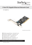
1
WAFER-8522 Motherboard
WAFER-8522 Motherboard
Page i
WAFER-8522otherboard
Revision
MODEL
WAFER-8522 Intel® Celeron® M Motherboard
Revision Number
Description
Date of Issue
1.0
Initial release
March 2007
Page ii
WAFER-8522 Motherboard
Copyright
COPYRIGHT NOTICE
The information in this document is subject to change without prior notice in order to
improve reliability, design and function and does not represent a commitment on the part
of the manufacturer.
In no event will the manufacturer be liable for direct, indirect, special, incidental, or
consequential damages arising out of the use or inability to use the product or
documentation, even if advised of the possibility of such damages.
This document contains proprietary information protected by copyright. All rights are
reserved. No part of this manual may be reproduced by any mechanical, electronic, or
other means in any form without prior written permission of the manufacturer.
TRADEMARKS
IBM PC is a registered trademark of International Business Machines Corporation. INTEL
is a registered trademark of INTEL Corporation. Other product names mentioned herein
are used for identification purposes only and may be trademarks and/or registered
trademarks of their respective owners.
Page iii
WAFER-8522otherboard
Packing List
NOTE:
If any of the components listed in the checklist below are missing,
please do not proceed with the installation. Contact the IEI reseller or
vendor you purchased the WAFER-8522 from or contact an IEI sales
representative directly. To contact an IEI sales representative, please
send an email to [email protected].
The items listed below should all be included in the WAFER-8522 package.
1 x WAFER-8522 single board computer
1 x Enclosure heat sink
1 x Audio cable
1 x IDE flat cable 44p/44p
1 x PS2 keyboard/mouse cable
1 x 4 COM port RS-232 cable
1 x Mini jumper pack
1 x Quick installation guide
1 x Utility CD
Images of the above items are shown in Chapter 3.
Page iv
WAFER-8522 Motherboard
Table of Contents
1
INTRODUCTION..................................................................................................... 3
1.1 WAFER-8522 OVERVIEW.......................................................................................... 4
1.1.1 WAFER-8522 Board Variations ......................................................................... 4
1.1.2 WAFER-8522 Applications ................................................................................ 4
1.1.3 WAFER-8522 Benefits........................................................................................ 4
1.1.4 WAFER-8522 Features ...................................................................................... 5
1.2 WAFER-8522 BOARD OVERVIEW ............................................................................. 6
1.2.1 WAFER-8522 Connectors .................................................................................. 7
1.2.2 Technical Specifications..................................................................................... 8
2
DETAILED SPECIFICATIONS ............................................................................11
2.1 OVERVIEW ............................................................................................................... 12
2.2 DIMENSIONS ............................................................................................................ 12
2.2.1 Board Dimensions............................................................................................ 12
2.2.2 External Interface Panel Dimensions .............................................................. 13
2.2.3 Enclosure Heat Sink Dimensions ..................................................................... 13
2.3 DATA FLOW .............................................................................................................. 15
2.4 COMPATIBLE PROCESSOR ......................................................................................... 16
2.4.1 CPU Overview ................................................................................................. 16
2.4.2 Intel® Celeron® M............................................................................................ 16
2.5 INTEL® 855GME CHIPSET GRAPHICS MEMORY CONTROLLER HUB ........................ 16
2.5.1 Intel® 852GM Overview................................................................................... 16
2.5.2 Intel® 852GM Memory Support....................................................................... 17
2.5.3 Intel® 852GM Internal Graphics Controller ................................................... 17
2.6 INTEL® 82801DB I/O CONTROLLER HUB (ICH4).................................................... 19
2.6.1 Intel® ICH4 Overview ...................................................................................... 19
2.6.2 Intel® ICH4 IDE Interface ............................................................................... 19
2.6.3 Intel® ICH4 Compact Flash Interface ............................................................. 20
2.6.4 Intel® ICH4 Audio Codec 97 (AC’97) Controller............................................ 20
2.6.5 Intel® ICH4 USB Controller ............................................................................ 21
2.6.6 Intel® ICH4 PCI Interface ............................................................................... 22
Page v
WAFER-8522otherboard
2.6.7 Intel® ICH4 Low Pin Count (LPC) Interface................................................... 22
2.6.8 BIOS................................................................................................................. 22
2.7 PCI BUS COMPONENTS ............................................................................................ 22
2.7.1 PCI Bus Overview............................................................................................ 22
2.7.2 GbE Ethernet ................................................................................................... 23
2.7.3 PCI-104 Slot..................................................................................................... 24
2.8 LPC BUS COMPONENTS ........................................................................................... 24
2.8.1 LPC Bus Overview........................................................................................... 24
2.8.2 BIOS Chipset.................................................................................................... 24
2.8.3 Super I/O Chipset............................................................................................. 24
2.8.3.1 Super I/O 16C550 UARTs ........................................................................ 25
2.8.3.2 Super I/O Keyboard Controller................................................................. 25
2.9 TPM MODULE ......................................................................................................... 25
2.10 ENVIRONMENTAL AND POWER SPECIFICATIONS ..................................................... 26
2.10.1 System Monitoring ......................................................................................... 26
2.10.2 Operating Temperature and Temperature Control......................................... 26
2.10.3 Power Consumption....................................................................................... 27
3
UNPACKING .......................................................................................................... 29
3.1 ANTI-STATIC PRECAUTIONS ...................................................................................... 30
3.2 UNPACKING.............................................................................................................. 30
3.2.1 Unpacking Precautions.................................................................................... 30
3.3 UNPACKING CHECKLIST ........................................................................................... 31
3.3.1 Package Contents............................................................................................. 31
4
CONNECTOR PINOUTS...................................................................................... 33
4.1 PERIPHERAL INTERFACE CONNECTORS .................................................................... 34
4.1.1 WAFER-8522 Layout ....................................................................................... 34
4.1.2 Peripheral Interface Connectors ..................................................................... 34
4.1.3 External Interface Panel Connectors............................................................... 35
4.2 INTERNAL PERIPHERAL CONNECTORS ...................................................................... 36
4.2.1 AT Power Connector........................................................................................ 36
4.2.2 ATX Power Connector ..................................................................................... 37
4.2.3 Audio Connector .............................................................................................. 38
4.2.4 Compact Flash Socket...................................................................................... 39
Page vi
WAFER-8522 Motherboard
4.2.5 IDE Connector ................................................................................................. 40
4.2.6 Inverter Power Connector ............................................................................... 42
4.2.7 Keyboard/Mouse Connector ............................................................................ 43
4.2.8 LED Connector ................................................................................................ 44
4.2.9 PCI-104 Slot..................................................................................................... 45
4.2.10 Power Button Connector................................................................................ 49
4.2.11 Reset Button Connector.................................................................................. 49
4.2.12 Serial Port Connector (RS-232/422/485) ...................................................... 50
4.2.13 Serial Port Connector (COM 3, COM 4, COM 5 and COM 6)..................... 51
4.2.14 TFT LCD LVDS Connector............................................................................ 53
4.2.15 Internal USB Connectors............................................................................... 54
4.3 EXTERNAL PERIPHERAL INTERFACE CONNECTORS .................................................. 55
4.3.1 External Peripheral Interface Connector Overview........................................ 55
4.3.2 RJ-45 Ethernet Connector ............................................................................... 56
4.3.3 Serial Port Connector (COM1) ....................................................................... 57
4.3.4 USB Combo Ports ............................................................................................ 58
4.3.5 VGA Connector ................................................................................................ 58
5
INSTALLATION .................................................................................................... 61
5.1 ANTI-STATIC PRECAUTIONS ...................................................................................... 62
5.2 INSTALLATION CONSIDERATIONS ............................................................................. 63
5.2.1 Installation Notices .......................................................................................... 63
5.2.2 Installation Checklist ....................................................................................... 64
5.3 SO-DIMM MODULE INSTALLATION AND CF CARD INSTALLATION ......................... 65
5.3.1 SO-DIMM Installation ..................................................................................... 65
5.3.2 CF Card Installation........................................................................................ 66
5.3.3 Mounting the WAFER-8522 Embedded Module .............................................. 67
5.4 JUMPER SETTINGS .................................................................................................... 69
5.4.1 CF Card Setup Jumper Settings....................................................................... 70
5.4.2 Clear CMOS Jumper........................................................................................ 71
5.4.3 COM Port Setting Jumper ............................................................................... 72
5.4.4 LCD Voltage Selection ..................................................................................... 73
5.4.5 LCD Resolution Selection ................................................................................ 74
5.5 CHASSIS INSTALLATION ........................................................................................... 76
5.5.1 Airflow.............................................................................................................. 76
Page vii
WAFER-8522otherboard
5.5.2 Motherboard Installation................................................................................. 76
5.6 INTERNAL PERIPHERAL DEVICE CONNECTIONS........................................................ 76
5.6.1 Peripheral Device Cables ................................................................................ 76
5.6.2 ATA Flat Cable Connection ............................................................................. 77
5.6.3 Audio Kit Installation....................................................................................... 78
5.6.4 Keyboard/Mouse Y-cable Connector ............................................................... 79
5.6.5 Four Serial Port Connector Cable .................................................................. 80
5.7 EXTERNAL PERIPHERAL INTERFACE CONNECTION ................................................... 81
6
AMI BIOS................................................................................................................ 83
6.1 INTRODUCTION ........................................................................................................ 84
6.1.1 Starting Setup................................................................................................... 84
6.1.2 Using Setup ...................................................................................................... 84
6.1.3 Getting Help..................................................................................................... 85
6.1.4 Unable to Reboot After Configuration Changes.............................................. 85
6.1.5 BIOS Menu Bar................................................................................................ 85
6.2 MAIN ....................................................................................................................... 86
6.3 ADVANCED ............................................................................................................... 87
6.3.1 CPU Configuration.......................................................................................... 88
6.3.2 IDE Configuration ........................................................................................... 90
6.3.2.1 IDE Master, IDE Slave ............................................................................. 93
6.3.3 Super IO Configuration.................................................................................... 97
6.3.4 Hardware Health Configuration.................................................................... 104
6.3.5 MPS Configuration ........................................................................................ 105
6.3.6 Trusted Computing......................................................................................... 106
6.3.7 USB Configuration......................................................................................... 106
6.3.7.1 USB Mass Storage Device Configuration............................................... 109
6.4 BOOT ......................................................................................................................110
6.4.1 Boot Settings Configuration............................................................................ 111
6.4.2 Boot Device Priority .......................................................................................113
6.4.3 Removable Drives ...........................................................................................114
6.5 SECURITY................................................................................................................115
6.6 CHIPSET ..................................................................................................................117
6.6.1 NorthBridge Configuration.............................................................................117
6.6.2 SouthBridge Configuration............................................................................ 123
Page viii
WAFER-8522 Motherboard
6.7 POWER KEY ........................................................................................................... 124
6.8 EXIT ....................................................................................................................... 126
7
SOFTWARE DRIVERS ....................................................................................... 129
7.1 AVAILABLE SOFTWARE DRIVERS ............................................................................ 130
7.2 CHIPSET DRIVER INSTALLATION............................................................................. 130
7.3 REALTEK AUDIO DRIVER INSTALLATION ............................................................... 133
7.4 INTEL GRAPHICS MEDIA ACCELERATOR DRIVER ................................................... 136
7.5 LAN DRIVER INSTALLATION ................................................................................. 138
A
BIOS OPTIONS .................................................................................................... 141
B
WATCHDOG TIMER .......................................................................................... 145
C
ADDRESS MAPPING.......................................................................................... 149
C.1 ADDRESS MAP ....................................................................................................... 150
C.2 1ST MB MEMORY ADDRESS MAP ......................................................................... 150
C.3 IRQ MAPPING TABLE ............................................................................................ 151
C.4 DMA CHANNEL ASSIGNMENTS ............................................................................. 151
D
EXTERNAL AC’97 AUDIO CODEC ................................................................. 153
D.1 INTRODUCTION ..................................................................................................... 154
D.1.1 Accessing the AC’97 CODEC ....................................................................... 154
D.1.2 Driver Installation......................................................................................... 154
D.2 SOUND EFFECT CONFIGURATION........................................................................... 154
D.2.1 Accessing the Sound Effects Manager .......................................................... 154
D.2.2 Sound Effect Manager Configuration Options ............................................. 156
INDEX............................................................................................................................ 159
Page ix
WAFER-8522otherboard
List of Figures
Figure 1-1: WAFER-8522 Overview .............................................................................6
Figure 1-2: WAFER-8522 Solder Side Overview ........................................................6
Figure 2-1: WAFER-8522 Dimensions (mm) .............................................................12
Figure 2-2: External Interface Panel Dimensions (mm)...........................................13
Figure 2-3: Enclosure Heat Sink Dimensions (mm).................................................14
Figure 2-4: Data Flow Block Diagram........................................................................15
Figure 4-1: Connector and Jumper Locations .........................................................34
Figure 4-2: AT Power Connector Location ...............................................................36
Figure 4-3: ATX Power Connector Location.............................................................37
Figure 4-4: Audio Connector Pinouts .......................................................................38
Figure 4-5: CF Card Socket Location ........................................................................39
Figure 4-6: IDE Device Connector Location .............................................................41
Figure 4-7: Inverter Connector Location...................................................................43
Figure 4-8: Keyboard/Mouse Connector Location...................................................44
Figure 4-9: LED Connector Locations.......................................................................45
Figure 4-10: PCI-104 Slot Location............................................................................48
Figure 4-11: Power Button Connector Location ......................................................49
Figure 4-12: Reset Button Connector Locations .....................................................50
Figure 4-13: Serial Port Connector Location............................................................51
Figure 4-14: RS-232 Serial Port Connector Location ..............................................52
Figure 4-15: TFT LCD LVDS Connector Pinout Locations......................................53
Figure 4-16: Internal USB Connector Location ........................................................55
Figure 4-17: WAFER-8522 On-board External Interface Connectors.....................56
Figure 4-18: LAN Connector ......................................................................................57
Figure 4-19: Serial Port Pinout Locations.................................................................58
Figure 4-20: VGA Connector ......................................................................................59
Figure 5-1: SO-DIMM Installation...............................................................................65
Page x
WAFER-8522 Motherboard
Figure 5-2: CF Card Installation.................................................................................67
Figure 5-3: Enclosure Heat Sink Retention Screws.................................................68
Figure 5-4: PCI-104 Module Installation (Hexagonal Copper Pillars).....................68
Figure 5-5: CF Card Setup Jumper Location............................................................71
Figure 5-6: JP2 Clear CMOS Jumper.........................................................................72
Figure 5-7: COM Port Setting Jumper Location.......................................................73
Figure 5-8: LCD Voltage Selection Jumper Location ..............................................74
Figure 5-9: LCD Resolution Jumper Location..........................................................75
Figure 5-10: IDE Cable Connection ...........................................................................77
Figure 5-11: IDE Cable Connection ...........................................................................78
Figure 5-12: Keyboard/mouse Y-cable Connection.................................................80
Figure 5-13: Four Serial Port Connector Cable Connection ...................................81
Figure 7-1: InstallShield Wizard Preparation Screen............................................ 131
Figure 7-2: Welcome Screen ................................................................................... 131
Figure 7-3: License Agreement............................................................................... 131
Figure 7-4: Readme Information ............................................................................. 132
Figure 7-5: Restart the Computer ........................................................................... 132
Figure 7-6: Audio Driver Install Shield Wizard Starting ....................................... 133
Figure 7-7: Audio Driver Setup Preparation .......................................................... 133
Figure 7-8: Audio Driver Welcome Screen ............................................................ 134
Figure 7-9: Audio Driver Software Configuration ................................................. 134
Figure 7-10: Audio Driver Digital Signal ................................................................ 135
Figure 7-11: Audio Driver Installation Begins ....................................................... 135
Figure 7-12: Audio Driver Installation Complete................................................... 136
Figure 7-13: GMA Driver Installation Welcome Screen ........................................ 137
Figure 7-14: GMA Driver License Agreement........................................................ 137
Figure 7-15: GMA Driver Installing Notice ............................................................. 138
Figure 7-16: GMA Driver Installation Complete .................................................... 138
Figure 7-17: LAN License Agreement .................................................................... 139
Figure 7-18: Select the Driver Directory ................................................................ 139
Figure 7-19: LAN Driver Configuration .................................................................. 140
Page xi
WAFER-8522otherboard
List of Tables
Table 1-1: WAFER-8522 Board Variations ..................................................................4
Table 1-2: Technical Specifications ............................................................................9
Table 2-1: Supported Processors..............................................................................16
Table 2-2: Supported HDD Specifications ................................................................20
Table 2-3: Power Consumption .................................................................................27
Table 3-1: Package List Contents..............................................................................32
Table 4-1: Peripheral Interface Connectors..............................................................35
Table 4-2: Rear Panel Connectors.............................................................................36
Table 4-3: AT Power Connector Pinouts ..................................................................37
Table 4-4: ATX Power Connector Pinouts ................................................................38
Table 4-5: Audio Connector Pinouts .........................................................................38
Table 4-6: CF Card Socket Pinouts ...........................................................................40
Table 4-7: IDE Connector Pinouts .............................................................................42
Table 4-8: Inverter Power Connector Pinouts ..........................................................43
Table 4-9: Keyboard/Mouse Connector Pinouts ......................................................44
Table 4-10: LED Connector Pinouts ..........................................................................45
Table 4-11: PCI-104 Slot Connector Pinouts ............................................................49
Table 4-12: Power Button Connector Pinouts..........................................................49
Table 4-13: Reset Button Connector Pinouts...........................................................50
Table 4-14: RS-232/422/485 Serial Port Connector Pinouts....................................51
Table 4-15: RS-232 Serial Port Connector Pinouts..................................................53
Table 4-16: TFT LCD LVDS Port Connector Pinouts ...............................................54
Table 4-17: Internal USB Connector Pinouts ...........................................................55
Table 4-18: RJ-45 Ethernet Connector Pinouts........................................................56
Table 4-19: RJ-45 Ethernet Connector LEDs............................................................57
Table 4-20: RS-232 Serial Port (COM 1) Pinouts ......................................................57
Table 4-21: USB Connector Pinouts..........................................................................58
Table 4-22: VGA Connector Pinouts .........................................................................59
Page xii
WAFER-8522 Motherboard
Table 5-1: Jumpers ....................................................................................................70
Table 5-2: CF Card Setup Jumper Settings ..............................................................70
Table 5-3: JP2 Clear CMOS Jumper Settings...........................................................71
Table 5-4: COM Port Setting Jumper Settings .........................................................72
Table 5-5: LCD Voltage Selection Jumper Settings.................................................74
Table 5-6: LCD Resolution Jumper Settings ............................................................75
Table 5-7: IEI Provided Cables...................................................................................76
Table 6-1: BIOS Navigation Keys...............................................................................85
Page xiii
WAFER-8522otherboard
BIOS Menus
Menu 1: Main
....................................................................................................86
Menu 2: Advanced ....................................................................................................88
Menu 3: CPU Configuration .......................................................................................89
Menu 4: IDE Configuration .........................................................................................90
Menu 5: IDE Master and IDE Slave Configuration ...................................................94
Menu 6: Super IO Configuration ................................................................................98
Menu 7: Hardware Health Configuration ............................................................... 104
Menu 8: MPS Configuration .................................................................................... 105
Menu 9: Trusted Computing ................................................................................... 106
Menu 10: USB Configuration .................................................................................. 107
Menu 11: USB Mass Storage Device Configuration.............................................. 109
Menu 12: Boot
................................................................................................. 111
Menu 13: Boot Settings Configuration................................................................... 112
Menu 14: Boot Device Priority Settings ................................................................. 114
Menu 15: Removable Drives ................................................................................... 115
Menu 16: Security
................................................................................................. 116
Menu 17: Chipset
................................................................................................. 117
Menu 18:NorthBridge Chipset Configuration........................................................ 118
Menu 19:SouthBridge Chipset Configuration ....................................................... 123
Menu 20:Power
................................................................................................. 124
Menu 21:Exit
................................................................................................. 126
Page xiv
WAFER-8522 Motherboard
Glossary
AC ’97
Audio Codec 97
IDE
Integrated Data Electronics
ACPI
Advanced Configuration and
I/O
Input/Output
Power Interface
ICH4
I/O Controller Hub 4
APM
Advanced Power Management
L1 Cache Level 1 Cache
ARMD
ATAPI Removable Media Device
L2 Cache Level 2 Cache
ASKIR
Shift Keyed Infrared
LCD
Liquid Crystal Display
ATA
Advanced Technology
LPT
Parallel Port Connector
Attachments
LVDS
Low Voltage Differential Signaling
BIOS
Basic Input/Output System
MAC
Media Access Controller
CFII
Compact Flash Type 2
OS
Operating System
CMOS
Complementary Metal Oxide
PCI
Peripheral Connect Interface
Semiconductor
PIO
Programmed Input Output
CPU
Central Processing Unit
PnP
Plug and Play
Codec
Compressor/Decompressor
POST
Power On Self Test
COM
Serial Port
RAM
Random Access Memory
DAC
Digital to Analog Converter
SATA
Serial ATA
DDR
Double Data Rate
S.M.A.R.T Self Monitoring Analysis and
DIMM
Dual Inline Memory Module
DIO
Digital Input/Output
SPD
Serial Presence Detect
DMA
Direct Memory Access
S/PDI
Sony/Philips Digital Interface
EIDE
Enhanced IDE
SDRAM
Synchronous Dynamic Random
EIST
Enhanced Intel SpeedStep
Reporting Technology
Access Memory
Technology
SIR
Serial Infrared
FFIO
Flexible File Input/Output
UART
Universal Asynchronous
FIFO
First In/First Out
FSB
Front Side Bus
USB
Universal Serial Bus
IrDA
Infrared Data Association
VGA
Video Graphics Adapter
HDD
Hard Disk Drive
Receiver-transmitter
Page xv
WAFER-8522 Motherboard
THIS PAGE IS INTENTIONALLY LEFT BLANK
Page 2
WAFER-8522 Motherboard
Chapter
1
1 Introduction
Page 3
WAFER-8522 Motherboard
1.1 WAFER-8522 Overview
The WAFER-8522 is a fanless single board computer using the Intel® Celeron® M
processor with high performance and low power consumption. The WAFER-8522 is
shipped with an enclosure heat sink for maximum heat dissipation. The WAFER-8522
also comes with an expansion PCI-104 slot which allows flexible implementations. The
WAFER-8522 supports various peripheral device interfaces, including Ethernet ports,
serial ports, USB 2.0 ports and VGA port. Multiple display support adds versatility to the
system enabling system integrators and designers increased flexibility in selecting
display panel options.
1.1.1 WAFER-8522 Board Variations
Four IEI WAFER-8522 models are available. The models are listed in Table 1-1.
WAFER-8522 CPU
Clock Speed—
Cashe
FSB
TPM
Ultra Low Voltage
-1GZ-R10
Intel Celeron M
1 GHz
Zero cache
400 MHz
No
-600-R10
Intel Celeron M
600 MHz
512 KB L2 cache
400 MHz
No
T-1GZ-R10
Intel Celeron M
1 GHz
Zero cache
400 MHz
Yes
T-600-R10
Intel Celeron M
600 MHz
512 KB L2 cache
400 MHz
Yes
Table 1-1: WAFER-8522 Board Variations
1.1.2 WAFER-8522 Applications
The WAFER-8522 is designed for applications in the following areas:
Kiosks and Point of Sales
Restaurants
Human Machine Interface (HMI) applications
Marine, GPS and transportation applications
Financial, retail and kiosk applications
1.1.3 WAFER-8522 Benefits
Some of the WAFER-8522 benefits include:
Page 4
WAFER-8522 Motherboard
Reduced hardware costs
Reduced software costs
Reduced maintenance costs
Client crash prevention
Central resource control
Security protection
1.1.4 WAFER-8522 Features
Some of the WAFER-8522 features are listed below:
3.5” form factor
RoHS compliant
Fanless design
ULV Intel® Celeron® M processor installed
Digital dual-independent display functionality
Two high performance gigabit Ethernet controllers on-board
CPU and chipset on the solder side for easy system thermal control
CompactFlash® card and PCI-104 slot solutions
Integrated audio
TPM v1.2 hardware security function supported
Page 5
WAFER-8522 Motherboard
1.2 WAFER-8522 Board Overview
Figure 1-1: WAFER-8522 Overview
Figure 1-2: WAFER-8522 Solder Side Overview
Page 6
WAFER-8522 Motherboard
1.2.1 WAFER-8522 Connectors
The WAFER-8522 has the following connectors on-board:
1 x AT power connector
1 x ATX power connector
1 x Audio connector
1 x Compact Flash (CF) connector
1 x IDE Interface connector
1 x Inverter connector
1 x Keyboard/mouse connector
1 x LED connector
1 x PCI-104 connector
1 x Power button connector
1 x Reset button connector
1 x RS-232/422/485 serial port connector
1 x RS-232 serial port connector (COM3~COM6)
1 x TFT LCD LVDS connector
1 x USB connector
The WAFER-8522 has the following connectors on the board rear panel:
1 x VGA connector
1 x Serial port connector
2 x USB 2.0 connectors
2 x LAN RJ-45 connectors
The WAFER-8522 has the following on-board jumpers:
Clear CMOS
CF Card Setup
COM Port Jumper Settings
LCD Voltage Setup
LCD Panel Resolution Setup
Page 7
WAFER-8522 Motherboard
1.2.2 Technical Specifications
WAFER-8522 technical specifications are listed in Table 1-2. Detailed descriptions of
each specification can be found in Chapter 2.
Specification
WAFER-8522
CPU (On-board)
Intel® Celeron M 600Mhz 512K cache / 1.0GHz zero cache
System Chipset
Intel® 852GM + ICH4
CRT integrated in Intel® 852GM
Display
Dual channel 18-bit LVDS
Memory
Supports one 200-pin DDR 266 SO-DIMM module up to 1GB
BIOS
AMI BIOS
SSD
CompactFlash® Type II
Audio
AC'97 Codec Realtek ALC655
LAN
Dual Realtek RTL8110SC GbE
Five RS-232 and
COM
One RS-232/RS-422/RS-485
USB2.0
Four USB 1.1 or USB 2.0 devices supported
IDE
One 44-pin IDE connects to two Ultra ATA33/66/100 devices
TPM
One TPM v1.2 module (SINOSUN SSX35) onboard
Watchdog Timer
Software programmable 1-255 sec. by supper I/O
IrDA
One IrDA connector
Expansion
One PCI-104 slot
Power Supply
AT/ATX power support
Page 8
WAFER-8522 Motherboard
Temperature
0ºC - 60ºC
Humidity (operating)
5%~95% non-condensing
Dimensions
146mm x 102mm
Weight (GW/NW)
700g/175g
Table 1-2: Technical Specifications
Page 9
WAFER-8522 Motherboard
THIS PAGE IS INTENTIONALLY LEFT BLANK
Page 10
WAFER-8522 Motherboard
Chapter
2
2 Detailed Specifications
Page 11
WAFER-8522 Motherboard
2.1 Overview
This chapter describes the specifications and on-board features of the WAFER-8522 in
detail.
2.2 Dimensions
2.2.1 Board Dimensions
The dimensions of the board are listed below:
Length:
146mm
Width:
102mm
Figure 2-1: WAFER-8522 Dimensions (mm)
Page 12
WAFER-8522 Motherboard
2.2.2 External Interface Panel Dimensions
External peripheral interface connector panel dimensions are shown in Figure 2-2.
Figure 2-2: External Interface Panel Dimensions (mm)
2.2.3 Enclosure Heat Sink Dimensions
The dimensions of the WAFER-8522 with the enclosure heat sink are shown in Figure
2-3.
Page 13
WAFER-8522 Motherboard
Figure 2-3: Enclosure Heat Sink Dimensions (mm)
Page 14
WAFER-8522 Motherboard
2.3 Data Flow
The WAFER-8522 motherboard comes with an Intel® Celeron M CPU. Figure 2-4 shows
the data flow between the system chipset, the CPU and other components installed on the
motherboard.
Figure 2-4: Data Flow Block Diagram
Page 15
WAFER-8522 Motherboard
2.4 Compatible Processor
2.4.1 CPU Overview
The ULV Intel® Celeron® M processor is installed on the WAFER-8522 motherboard.
Specifications for the processors are listed in Table 2-1 below:
Family
Architecture
Cache
Clock Speed
FSB
ULV Intel® Celeron® M
90 nm
512 KB L2
1.0 GHz
400 MHz
ULV Intel® Celeron® M
90 nm
512 KB L2
600 MHz
400 MHz
Table 2-1: Supported Processors
2.4.2 Intel® Celeron® M
The (ULV) Intel® Celeron® M processor comes with the following features:
Intel® Streaming SIMD Extensions accelerates 3D graphics performance,
video decoding/encoding, and speech recognition.
Advanced power management features
Compatible with IA-32 software.
Advanced branch prediction and data prefetch logic
2.5 Intel® 855GME Chipset Graphics Memory Controller Hub
2.5.1 Intel® 852GM Overview
The Intel® 852GM chipset comes with the following features:
Supports Intel® NetBurst® micro-architecture
400 MHz system bus delivers a high-bandwidth connection between the
processor and the platform
Supports integrated graphics utilizing Intel® Extreme Graphics 2 technology
Three USB host controllers provide high performance peripherals with 480
Mbps of bandwidth, while enabling support for up to six USB 2.0 ports.
The latest AC ’97 implementation delivers 20-bit audio for enhanced sound
quality and full surround-sound capability.
Page 16
WAFER-8522 Motherboard
LAN Connect Interface (LCI) provides flexible network solutions such as
10/100 Mbps Ethernet and 10/100 Mbps Ethernet with LAN manageability
Dual Ultra ATA/100 controllers, coupled with the Intel® Application Accelerator
supports faster IDE transfers to storage devices
Intel Application Accelerator software provides additional performance over
native ATA drivers by improving I/O transfer rates and enabling faster O/S
load time, resulting in accelerated boot times
2.5.2 Intel® 852GM Memory Support
The Intel® 852GM supports one DDR memory module with frequencies up to 266MHz.
The WAFER-8522 has one 200-pin DDR SDRAM SO-DIMM socket that supports one
200MHz or 266MHz DDR SO-DIMM memory module with a maximum capacity of 1GB.
2.5.3 Intel® 852GM Internal Graphics Controller
The Intel® Extreme Graphics 2 is integrated on the Intel® 852GM Northbridge chipset.
The Intel® Extreme Graphics 2 features are listed below.
Enhanced Rapid Pixel and Texel Rendering: Optimized visual quality and
performance from the addition of hardware to support of texel formatting,
bicubic filter, color blending accuracy, and video mixing render, resulting in
optimized visual quality and performance.
Zone Rendering 2 Technology: Enhances the performance of zone
rendering by using larger zones and new commands that improve graphics
pipeline efficiency.
Dynamic Video Memory Technology v2.0: Increases total system
performance by optimizing the efficiency of AGP dynamic video memory by
increasing its size of Video RAM allocation to 96 MB.
Enhanced Intelligent Memory Management: Improves memory bandwidth
efficiency and platform performance by improving the memory management
arbitration between CPU, system memory and graphics memory.
Intel® Extreme Graphics 2 specifications are listed below:
Enhanced 2D:
Page 17
WAFER-8522 Motherboard
o
o
o
o
o
o
o
o
o
o
256-bit internal path
8/16/32bpp
DirectDraw*, GDI, GDI+
Anti-aliased text support
Alpha blending
Alphas stretch blitter
Hardware alpha blended RGB cursor
Color space conversion
5x2 overlay support
Rotate, scale and translate operations
High-performance 3D:
o
o
o
o
o
o
o
o
o
o
256-bit internal path
32bpp/ 24ZorW/ 8 Stencil
DX7*/DX8*/OGL*1.1
DXTn texture compression
Up to 4 textures / pixel on a single pass
Cubic reflection map
Embossed/DOT3 bump mapping
Multi-texture
DOT3 bump-mapping
Point sprites
Video and Display:
o
o
o
o
o
o
DirectShow*/DirectVA*
Hardware motion compensation support for DVD playback
4x2 overlay filter
350 MHz DAC frequency
Maximum DVO pixel rate of up to 330MP/s
Flat panel monitors and TV-out support via AGP Digital Display (ADD)
cards
o
350 MHz DAC for 1800x1440 @ 85Hz max CRT resolution or
2048x1536@60Hz max FP resolution
o
o
o
Synchronous display for dual monitor capabilities
350MHz RAMDAC for up to QXGA analog monitor support
Dual DVO ports for up to QXGA digital display support
Multiple display types (LVDS, DVI, TV-out, CRT)
Page 18
WAFER-8522 Motherboard
2.6 Intel® 82801DB I/O Controller Hub (ICH4)
2.6.1 Intel® ICH4 Overview
The Intel® ICH4 I/O controller hub comes with the following features:
PCI Local Bus Specification, Revision 2.2-compliant with support for 33 MHz
PCI operations.
ACPI Power Management Logic Support
Enhanced DMA controller, Interrupt controller, and timer functions
Integrated IDE controller supports Ultra ATA100/66/33
USB host interface with support for 4 USB ports; 3 UHCI host controllers; 1
EHCI high-speed
USB 2.0 Host controller
Integrated LAN controller
System Management Bus (SMBus) Specification, Version 2.0 with additional
support for I2C devices
Supports Audio Codec ’97, Revision 2.3 specification
Low Pin Count (LPC) interface
Firmware Hub (FWH) interface support
Alert On LAN* (AOL) and Alert On LAN 2* (AOL2)
2.6.2 Intel® ICH4 IDE Interface
The single WAFER-8522 IDE connector supports two IDE hard disks and ATAPI devices.
PIO IDE transfers up to 16MB/s and Ultra ATA transfers of 100MB/s. The integrated IDE
interface is able to support the following IDE HDDs:
The onboard ATA-6 controller is able to support the following IDE HDDs:
Ultra ATA/100, with data transfer rates up to 100MB/s
Ultra ATA/66, with data transfer rates up to 66MB/s
Ultra ATA/33, with data transfer rates up to 33MB/s
Page 19
WAFER-8522 Motherboard
Specification
Ultra ATA/100
Ultra ATA/66
Ultra ATA/100
IDE devices
2
2
2
PIO Mode
0–4
0–4
0–4
PIO Max Transfer Rate
16.6 MB/s
16.6 MB/s
16.6 MB/s
DMA/UDMA designation
UDMA 3 - 4
UDMA 3 – 4
UDMA 2
DMA/UDMA Max Transfer
100MB/s
66MB/s
33MB/s
Controller Interface
5V
5V
5V
Table 2-2: Supported HDD Specifications
2.6.3 Intel® ICH4 Compact Flash Interface
The WAFER-8522 CompactFlash socket supports standard CF Type II cards. The chipset
flash interface is multiplexed with an IDE interface and can be connected to an array of
industry standard NAND Flash or NOR Flash devices.
2.6.4 Intel® ICH4 Audio Codec 97 (AC’97) Controller
The WAFER-8522 has an integrated REALTEK ALC655 CODEC. The ALC655 CODEC is
a 16-bit, full-duplex AC'97 Rev. 2.3 compatible six-channel audio CODEC designed for PC
multimedia systems, including host/soft audio and AMR/CNR-based designs. Some of the
features of the codec are listed below.
Meets performance requirements for audio on PC99/2001 systems
Meets Microsoft WHQL/WLP 2.0 audio requirements
16-bit Stereo full-duplex CODEC with 48KHz sampling rate
Compliant with AC'97 Rev 2.3 specifications
Front-Out, Surround-Out, MIC-In and LINE-In Jack Sensing
14.318MHz -> 24.576MHz PLL to eliminate crystal
12.288MHz BITCLK input
Integrated PCBEEP generator to save buzzer
Interrupt capability
Three analog line-level stereo inputs with 5-bit volume control, LINE_IN, CD,
Page 20
WAFER-8522 Motherboard
AUX
High-quality differential CD input
Two analog line-level mono inputs: PCBEEP, PHONE-IN
Two software selectable MIC inputs
Dedicated Front-MIC input for front panel applications (software selectable)
Boost preamplifier for MIC input
LINE input shared with surround output; MIC input shared with Center and
LFE output
Built-in 50mW/20ohm amplifier for both Front-out and Surround-Out
External Amplifier Power Down (EAPD) capability
Power management and enhanced power saving features
Supports Power-Off CD function
Adjustable VREFOUT control
Supports 48KHz S/PDIF output, complying with AC'97 Rev 2.3 specifications
Supports 32K/44.1K/48KHz S/PDIF input
Power support: Digital: 3.3V; Analog: 3.3V/5V
Standard 48-pin LQFP package
EAX™ 1.0 & 2.0 compatible
Direct Sound 3D™ compatible
A3D™ compatible
I3DL2 compatible
HRTF 3D positional audio
10-band software equalizer
Voice cancellation and key shifting in Karaoke mode
AVRack® Media Player
Configuration Panel for improved user convenience
2.6.5 Intel® ICH4 USB Controller
Two external USB ports on the WAFER-8522 board are interfaced to the chipset USB
controller. Four USB 1.1 or USB 2.0 devices can be connected simultaneously to the
WAFER-8522. The chipset USB controller has the following specifications:
4 USB ports
USB 1.1 and USB 2.0 compliant
Page 21
WAFER-8522 Motherboard
3 Universal Host Controller Interface (UHCI) controllers
High-speed, full-speed and low-speed capable
2.6.6 Intel® ICH4 PCI Interface
The PCI interface on the ICH4 is compliant with the PCI Revision 2.2 implementation.
Some of the features of the PCI interface are listed below.
PCI Revision 2.2 compliant
33MHz
5V tolerant PCI signals (except PME#)
Integrated PCI arbiter supports up to six PCI bus masters
2.6.7 Intel® ICH4 Low Pin Count (LPC) Interface
The ICH4 LPC interface complies with the LPC 1.0 specifications. The LPC bus from the
ICH4 is connected to the following components:
BIOS chipset
Super I/O chipset
2.6.8 BIOS
The BIOS flash memory chip on the WAFER-8522 has a licensed copy of AMI BIOS
loaded onto it. The BIOS flash memory chip is connected to the chipset via the LPC bus.
The flash BIOS features are listed below:
SMIBIOS (DMI) compliant
Console redirection function support
PXE (Pre-Boot Execution Environment) support
USB booting support
2.7 PCI Bus Components
2.7.1 PCI Bus Overview
Page 22
WAFER-8522 Motherboard
The PCI bus controller on the ICH4 is compliant with PCI Revision 2.2 specifications and
has a 33MHz PCI clock. The components listed below are all connected to the PCI bus:
PCI-104 socket
Realtek RTL8110SC GbE interface
2.7.2 GbE Ethernet
A highly integrated and cost-effective single-chip, fast RealTek RTL8110SC GbE Ethernet
controller is interfaced through first the PCI bus to the CPU and system chipset. The
RealTek RTL8110SC controller provides 10Mbps, 100Mbps or 1000Mbps Ethernet
connectivity to the WAFER-8522. Some of the features of the RealTek RTL8110SC are
listed below.
Integrated 10/100/1000 transceiver
Auto-Negotiation with Next Page capability
Supports PCI rev.2.3, 32-bit, 33/66MHz
Supports CLKRUNB and MiniPCI v1.0
Supports pair swap/polarity/skew correction
Crossover Detection & Auto-Correction
Wake-on-LAN and remote wake-up support
Microsoft® NDIS5 Checksum Offload (IP, TCP, UDP) and largesend offload
support
Supports Full Duplex flow control (IEEE 802.3x)
Fully compliant with IEEE 802.3, IEEE 802.3u, IEEE 802.3ab
Supports IEEE 802.1P Layer 2 Priority Encoding
Supports IEEE 802.1Q VLAN tagging
Serial EEPROM
3.3V signaling, 5V PCI I/O tolerant
Transmit/Receive FIFO (8K/64K) support
Supports power down/link down power saving
Supports PCI Message Signaled Interrupt (MSI)
Page 23
WAFER-8522 Motherboard
2.7.3 PCI-104 Slot
The PCI-104 socket supports PCI-104 modules that are compliant with PCI Specification,
Revision 1.0. The PCI-104 modules are easily installed into the socket. The standard
PCI-104 modules are 95.89mm wide, 90.17mm long.
2.8 LPC Bus Components
2.8.1 LPC Bus Overview
The LPC bus is connected to components listed below:
BIOS chipset
Super I/O chipset
2.8.2 BIOS Chipset
The BIOS chipset has a licensed copy of AMI BIOS installed on the chipset. Some of the
BIOS features are listed below:
AMI Flash BIOS
SMIBIOS (DMI) compliant
Console redirection function support
PXE (Pre-boot Execution Environment) support
USB booting support
2.8.3 Super I/O Chipset
The iTE IT8712F Super I/O chipset is connected to the ICH4 through the LPC bus. The
iTE IT8712F is an LPC interface-based Super I/O device that comes with Environment
Controller integration. Some of the features of the iTE IT8712F chipset are listed below:
LPC Interface
PC98/99/2001, ACPI and LANDesk Compliant
Enhanced Hardware Monitor
SmartGuardian Controller
Single +5V Power Supply
Page 24
WAFER-8522 Motherboard
Two 16C550 UARTs for serial port control
One IEEE 1284 Parallel Port
Keyboard Controller
Watchdog Timer
Serial IRQ Support
Vbat & Vcch Support
Single +5V Power Supply
Some of the Super I/O features are described in more detail below:
2.8.3.1 Super I/O 16C550 UARTs
The onboard Super I/O has two integrated 16C550 UARTs that can support the following:
Two standard serial ports (COM1 and COM2)
IrDa 1.0 and ASKIR protocols
Another chipset connected to the LPC bus provided connectivity to another four serial port
connectors (COM3, COM4, COM5 and COM6).
2.8.3.2 Super I/O Keyboard Controller
The Super I/O keyboard controller can execute the 8042 instruction set. Some of the
keyboard controller features are listed below:
The 8042 instruction is compatible with a PS/2 keyboard and PS/2 mouse
Gate A20 and Keyboard reset output
Supports multiple keyboard power on events
Supports mouse double-click and/or mouse move power on events
2.9 TPM Module
The WAFER-8522 has one SINOSUN SSX35 TPM v1.2 module on-board. Some of the
TPM module features are listed below:
Fully compatible with TCG v1.2 Specifications
SINOSUN 8-bit CPU core
Embedded 16KB secure data FLASH memory and 16KB RAM
Page 25
WAFER-8522 Motherboard
128KB program FLASH memory supporting online update of firmware
RSA engine supports up to 2048 bits RSA algorithm
Embedded SHA-1 algorithm engine
2.10 Environmental and Power Specifications
2.10.1 System Monitoring
Three thermal inputs on the WAFER-8522 Super I/O Enhanced Hardware Monitor monitor
the following temperatures:
System temperature
Temperature Sensor #1
Eight voltage inputs on the WAFER-8522 Super I/O Enhanced Hardware Monitor monitor
the following voltages:
CPU Core
VCC
+3.3V
+5.0V
+1.5V
VBAT
The WAFER-8522 Super I/O Enhanced Hardware Monitor also monitors the CPU fan
speeds.
2.10.2 Operating Temperature and Temperature Control
The maximum and minimum operating temperatures for the WAFER-8522 are listed
below.
Minimum Operating Temperature: 0ºC (32°F)
Maximum Operating Temperature: 60°C (140°F)
A cooling fan and heat sink must be installed on the CPU. Thermal paste must be
smeared on the lower side of the heat sink before it is mounted on the CPU. Heat sinks
Page 26
WAFER-8522 Motherboard
are also mounted on the northbridge and southbridge chipsets to ensure the operating
temperature of these chips remain low.
2.10.3 Power Consumption
Table 2-3 shows the power consumption parameters for the WAFER-8522 when an Intel®
Celeron® M 1.0GHz CPU is running with one 1GB 400MHz DDR SDRAM memory
module.
Voltage
Current
5V
3.43A
12V
0.13A
Table 2-3: Power Consumption
Page 27
WAFER-8522 Motherboard
THIS PAGE IS INTENTIONALLY LEFT BLANK
Page 28
WAFER-8522 Motherboard
Chapter
3
3 Unpacking
Page 29
WAFER-8522 Motherboard
3.1 Anti-static Precautions
WARNING:
Failure to take ESD precautions during the installation of the
WAFER-8522 may result in permanent damage to the WAFER-8522
and severe injury to the user.
Electrostatic discharge (ESD) can cause serious damage to electronic components,
including the WAFER-8522. Dry climates are especially susceptible to ESD. It is therefore
critical that whenever the WAFER-8522, or any other electrical component is handled, the
following anti-static precautions are strictly adhered to.
Wear an anti-static wristband: - Wearing a simple anti-static wristband can
help to prevent ESD from damaging the board.
Self-grounding:- Before handling the board touch any grounded conducting
material. During the time the board is handled, frequently touch any
conducting materials that are connected to the ground.
Use an anti-static pad: When configuring the WAFER-8522, place it on an
antic-static pad. This reduces the possibility of ESD damaging the
WAFER-8522.
Only handle the edges of the PCB:-: When handling the PCB, hold the PCB
by the edges.
3.2 Unpacking
3.2.1 Unpacking Precautions
When the WAFER-8522 is unpacked, please do the following:
Follow the anti-static precautions outlined in Section 3.1.
Make sure the packing box is facing upwards so the WAFER-8522 does not
fall out of the box.
Make sure all the components shown in Section 3.3 are present.
Page 30
WAFER-8522 Motherboard
3.3 Unpacking Checklist
NOTE:
If some of the components listed in the checklist below are missing,
please do not proceed with the installation. Contact the IEI reseller or
vendor you purchased the WAFER-8522 from or contact an IEI sales
representative directly. To contact an IEI sales representative, please
send an email to [email protected].
3.3.1 Package Contents
The WAFER-8522 is shipped with the following components:
Quantity
Item
1
WAFER-8522 single board computer
1
Enclosure heat sink
1
Audio cable
1
IDE flat cable 44p/44p
1
PS2 keyboard/mouse cable
Image
Page 31
WAFER-8522 Motherboard
1
4 COM port RS-232 cable
1
Mini jumper pack
1
Quick installation guide
1
Utility CD
Table 3-1: Package List Contents
Page 32
WAFER-8522 Motherboard
Chapter
4
4 Connector Pinouts
Page 33
WAFER-8522 Motherboard
4.1 Peripheral Interface Connectors
Section 4.1.2 shows peripheral interface connector locations. Section 4.1.2 lists all the
peripheral interface connectors seen in Section 4.1.2.
4.1.1 WAFER-8522 Layout
Figure 4-1 shows the on-board peripheral connectors, rear panel peripheral connectors
and on-board jumpers.
Figure 4-1: Connector and Jumper Locations
4.1.2 Peripheral Interface Connectors
Table 4-1 shows a list of the peripheral interface connectors on the WAFER-8522.
Detailed descriptions of these connectors can be found below.
Page 34
WAFER-8522 Motherboard
Connector
Type
Label
AT power connector
4-pin wafer connector
CN5
ATX power connector
3-pin wafer connector
CN8
Audio connector
10-pin box header
CN4
Compact Flash (CF) connector
50-pin CF slot
CF1
IDE Interface connector
44-pin box header
IDE1
Inverter connector
5-pin wafer connector
CN10
Keyboard/mouse connector
6-pin wafer connector
KB1
LED connector
6-pin header
CN3
PCI-104 connector
PCI-104 slot
J1
Power button connector
2-pin wafer connector
CN7
Reset button connector
2-pin wafer connector
CN6
RS-232/422/485 serial port connector
14-pin header
COM2
RS-232 serial port connector (COM3~COM6)
40-pin header
CN9
TFT LCD LVDS connector
30-pin crimp connector
LVDS1
USB connector
8-pin header
USB1
Table 4-1: Peripheral Interface Connectors
4.1.3 External Interface Panel Connectors
Table 4-2 lists the rear panel connectors on the WAFER-8522. Detailed descriptions of
these connectors can be found in Section 4.2.15 on page 54.
Connector
Type
Label
Ethernet connectors
RJ-45 connector
LAN1, LAN2
Page 35
WAFER-8522 Motherboard
RS-232 serial port connector
DB-9 connector
COM1
USB ports
USB port
J2
VGA port connector
15-pin female
VGA1
Table 4-2: Rear Panel Connectors
4.2 Internal Peripheral Connectors
Internal peripheral connectors are found on the motherboard and are only accessible
when the motherboard is outside of the chassis. This section has complete descriptions of
all the internal, peripheral connectors on the WAFER-8522.
4.2.1 AT Power Connector
CN Label:
CN5
CN Type:
4-pin wafer connector (1x4)
CN Location:
See Figure 4-2
CN Pinouts:
See Table 4-3
The 4-pin AT power connector is connected to an AT power supply.
Figure 4-2: AT Power Connector Location
Page 36
WAFER-8522 Motherboard
PIN NO.
DESCRIPTION
1
+12V
2
GROUND
3
GROUND
4
+5V
Table 4-3: AT Power Connector Pinouts
4.2.2 ATX Power Connector
CN Label:
CN8
CN Type:
3-pin wafer connector (1x3)
CN Location:
See Figure 4-3
CN Pinouts:
See Table 4-4
The 3-pin ATX power connector is connected to an ATX power supply.
Figure 4-3: ATX Power Connector Location
PIN NO.
DESCRIPTION
1
+5V_SB
2
GROUND
Page 37
WAFER-8522 Motherboard
3
PS_ON
Table 4-4: ATX Power Connector Pinouts
4.2.3 Audio Connector
CN Label:
CN4
CN Type:
10-pin box header (2x5)
CN Location:
See Figure 4-4
CN Pinouts:
See Table 4-5
The 10-pin audio connector is connected to speakers the output of audio signals from the
system.
Figure 4-4: Audio Connector Pinouts
PIN NO.
DESCRIPTION
PIN NO.
DESCRIPTION
1
LINEOUT_R
2
LINEIN_R
3
GROUND
4
GROUND
5
LINEOUT_L
6
LINEIN_L
7
GROUND
8
GROUND
9
MIC1IN
10
MIC2IN
Table 4-5: Audio Connector Pinouts
Page 38
WAFER-8522 Motherboard
4.2.4 Compact Flash Socket
CN Label:
CF1
CN Type:
50-pin CF slot (2x25)
CN Location:
See Figure 4-5
CN Pinouts:
See Table 4-6
A CF Type II memory card is inserted to the CF socket of the WAFER-8522.
Figure 4-5: CF Card Socket Location
PIN NO.
1
DESCRIPTION
GROUND
PIN NO.
26
DESCRIPTION
GROUND
Page 39
WAFER-8522 Motherboard
2
D3
27
D11
3
D4
28
D12
4
D5
29
D13
5
D6
30
D14
6
D7
31
D15
7
CS1#
32
CS3#
8
N/C
33
N/C
9
GROUND
34
IOR#
10
N/C
35
IOW#
11
N/C
36
VCC
12
N/C
37
IRQ15
13
VCC
38
VCC
14
N/C
39
MASTER/SLAVE
15
N/C
40
N/C
16
N/C
41
RESET#
17
N/C
42
IORDY
18
A2
43
DMARQ
19
A1
44
DMACK#
20
A0
45
ACTIVE#
21
D0
46
PDIAG#
22
D1
47
D8
23
D2
48
D9
24
N/C
49
D10
25
GROUND
50
GROUND
Table 4-6: CF Card Socket Pinouts
4.2.5 IDE Connector
CN Label:
IDE1
CN Type:
44-pin box header (2x22)
CN Location:
See Figure 4-6
CN Pinouts:
See Table 4-7
Page 40
WAFER-8522 Motherboard
One 44-pin IDE device connector on the WAFER-8522 supports connectivity to two hard
disk drives.
Figure 4-6: IDE Device Connector Location
PIN NO.
DESCRIPTION
PIN NO.
DESCRIPTION
1
RESET#
2
GROUND
3
DATA 7
4
DATA 8
5
DATA 6
6
DATA 9
7
DATA 5
8
DATA 10
9
DATA 4
10
DATA 11
11
DATA 3
12
DATA 12
Page 41
WAFER-8522 Motherboard
13
DATA 2
14
DATA 13
15
DATA 1
16
DATA 14
17
DATA 0
18
DATA 15
19
GROUND
20
N/C
21
DMARQ
22
GROUND
23
IOW#
24
GROUND
25
IOR#
26
GROUND
27
IORDY
28
BALE
29
DMACK#
30
GROUND
31
INTERRUPT
32
N/C
33
SA1
34
PDIAG
35
SA0
36
SA2
37
HDC CS0#
38
HDC CS1#
39
HDD ACTIVE#
40
GROUND
41
+5V
42
+5V
43
GROUND
44
N/C
Table 4-7: IDE Connector Pinouts
4.2.6 Inverter Power Connector
CN Label:
CN10
CN Type:
5-pin wafer connector (1x5)
CN Location:
See Figure 4-7
CN Pinouts:
See Table 4-8
The inverter connector is connected to the LCD backlight.
Page 42
WAFER-8522 Motherboard
Figure 4-7: Inverter Connector Location
PIN NO.
DESCRIPTION
1
INV_ADJ
2
GND
3
+12V
4
GND
5
(H)ON/OFF(L)
Table 4-8: Inverter Power Connector Pinouts
4.2.7 Keyboard/Mouse Connector
CN Label:
KB1
CN Type:
6-pin wafer connector (1x6)
CN Location:
See Figure 4-8
CN Pinouts:
See Table 4-9
The keyboard/mouse connector can be connected to a standard PS/2 cable or PS/2 cable
to add keyboard and mouse functionality to the system.
Page 43
WAFER-8522 Motherboard
Figure 4-8: Keyboard/Mouse Connector Location
PIN NO.
DESCRIPTION
1
+5V
2
MS DATA
3
MS CLK
4
KB DATA
5
KB CLK
6
GROUND
Table 4-9: Keyboard/Mouse Connector Pinouts
4.2.8 LED Connector
CN Label:
CN3
CN Type:
6-pin header (1x6)
CN Location:
See Figure 4-9
CN Pinouts:
See Table 4-10
The LED connector connects to an HDD indicator LED and a power LED on the system
chassis to inform the user about HDD activity and the power on/off status of the system.
Page 44
WAFER-8522 Motherboard
Figure 4-9: LED Connector Locations
PIN NO.
DESCRIPTION
1
+5V
2
GROUND
3
+5V
4
GROUND
5
HDLED+
6
HDLED-
Table 4-10: LED Connector Pinouts
4.2.9 PCI-104 Slot
CN Label:
J1
CN Type:
120-pin PCI-104 slot
CN Location:
See Figure 4-10
CN Pinouts:
See Table 4-11
The PCI-104 slot enables a PCI-104 compatible expansion module to be connected to the
board.
Page 45
WAFER-8522 Motherboard
Page 46
WAFER-8522 Motherboard
Page 47
WAFER-8522 Motherboard
Figure 4-10: PCI-104 Slot Location
Pin No.
Column A
Column B
Column C
Column D
1
GND/5V
TBD1
5V
AD00
2
VI/O1
AD02
AD01
+5V
3
AD05
GND
AD04
AD03
4
C/BE0#
AD07
GND
AD06
5
GND
AD09
AD08
GND
6
AD11
VI/O2
AD10
M66EN
7
AD14
AD13
GND
AD12
8
+3.3V
C/BE1#
AD15
+3.3V
9
SERR#
GND
SB0#
PAR
10
GND
PERR#
+3.3V
SDONE
11
STOP#
+3.3V
LOCK#
GND
12
+3.3V
TRDY#
GND
DEVSEL#
13
FRAME#
GND
IRDY#
+3.3V
14
GND
AD16
+3.3V
C/BE2#
15
AD18
+3.3V
AD17
GND
16
AD21
AD20
GND
AD19
17
+3.3V
AD23
AD22
+3.3V
18
IDSEL0
GND
IDSEL1
IDSEL2
19
AD24
C/BE3#
VI/O1
IDSEL3
20
GND
AD26
AD25
GND
21
AD29
+5V
AD28
AD27
22
+5V
AD30
GND
AD31
23
REQ0#
GND
REQ1#
VI/O2
24
GND
REQ2#
+5V
GNT0#
25
GNT1#
VI/O3
GNT2#
GND
26
+5V
CLK0
GND
CLK1
27
CLK2
+5V
CLK3
GND
Page 48
WAFER-8522 Motherboard
28
GND
INTD#
+5V
RST#
29
+12V
INTA#
INTB#
INTC#
30
-12V
TBD2
TBD
GND/3.3V
Table 4-11: PCI-104 Slot Connector Pinouts
4.2.10 Power Button Connector
CN Label:
CN7
CN Type:
2-pin wafer connector (1x2)
CN Location:
See Figure 4-11
CN Pinouts:
See Table 4-12
The power button connector is connected to a power switch on the system chassis to
enable users to turn the system on and off.
Figure 4-11: Power Button Connector Location
PIN NO.
DESCRIPTION
1
Button+
2
Button-
Table 4-12: Power Button Connector Pinouts
4.2.11 Reset Button Connector
Page 49
WAFER-8522 Motherboard
CN Label:
CN6
CN Type:
2-pin wafer connector (1x2)
CN Location:
See Figure 4-12
CN Pinouts:
See Table 4-13
The reset button connector is connected to a reset switch on the system chassis to enable
users to reboot the system when the system is turned on.
Figure 4-12: Reset Button Connector Locations
PIN NO.
DESCRIPTION
1
RESET#
2
GROUND
Table 4-13: Reset Button Connector Pinouts
4.2.12 Serial Port Connector (RS-232/422/485)
CN Label:
COM2
CN Type:
14-pin header (2x7)
CN Location:
See Figure 4-13
CN Pinouts:
See Table 4-14
The serial port connectors connect to RS-232, RS-422 or RS-485 serial port device.
Page 50
WAFER-8522 Motherboard
Figure 4-13: Serial Port Connector Location
PIN NO. DESCRIPTION
PIN NO. DESCRIPTION
1
DCD
2
DSR
3
RXD
4
RTS
5
TXD
6
CTS
7
DTR
8
RI
9
GND
10
GND
11
(RS422/485) TX+
12
(RS422/485) TX-
13
(RS422) RX+
14
(RS422) RX-
Table 4-14: RS-232/422/485 Serial Port Connector Pinouts
4.2.13 Serial Port Connector (COM 3, COM 4, COM 5 and COM 6)
CN Label:
CN9
CN Type:
40-pin header (2x20)
CN Location:
See Figure 4-14
CN Pinouts:
See Table 4-15
The 40-pin serial port connector contains the following four serial ports, COM 3, COM 4,
COM 5 and COM 6. All four serial ports are RS-232 serial communications channels. The
serial port locations are specified below.
COM 3 is located on pin 1 to pin 10
Page 51
WAFER-8522 Motherboard
COM 4 is located on pin 11 to pin 20
COM 5 is located on pin 21 to pin 30
COM 6 is located on pin 31 to pin 40
Figure 4-14: RS-232 Serial Port Connector Location
PIN NO. DESCRIPTION
PIN NO. DESCRIPTION
1
DCD_COM3
2
DSR_COM3
3
RXD_COM3
4
RTS_COM3
5
TXD_COM3
6
CTS_COM3
7
DTR_COM3
8
RI_COM3
9
GND
10
GND
11
DCD_COM4
12
DSR_COM4
13
RXD_COM4
14
RTS_COM4
15
TXD_COM4
16
CTS_COM4
17
DTR_COM4
18
RI_COM4
19
GND
20
GND
21
DCD_COM5
22
DSR_COM5
23
RXD_COM5
24
RTS_COM5
25
TXD_COM5
26
CTS_COM5
27
DTR_COM5
28
RI_COM5
29
GND
30
GND
Page 52
WAFER-8522 Motherboard
31
DCD_COM6
32
DSR_COM6
33
RXD_COM6
34
RTS_COM6
35
TXD_COM6
36
CTS_COM6
37
DTR_COM6
38
RI_COM6
39
GND
40
GND
Table 4-15: RS-232 Serial Port Connector Pinouts
4.2.14 TFT LCD LVDS Connector
CN Label:
J3
CN Type:
30-pin crimp connector (2x15)
CN Location:
See Figure 4-15
CN Pinouts:
See Table 4-16
The 30-pin TFT LCD LVDS can be connected to a TFT LCD screen directly.
Figure 4-15: TFT LCD LVDS Connector Pinout Locations
PIN NO. DESCRIPTION
1
GND
PIN NO. DESCRIPTION
2
GND
Page 53
WAFER-8522 Motherboard
3
Rin0+
4
Rin0-
5
Rin1+
6
Rin1-
7
Rin2+
8
Rin2-
9
CLK1+
10
CLK1-
11
Rin3+
12
Rin3-
13
GND
14
GND
15
Rin4+
16
Rin4-
17
Rin5+
18
Rin5-
19
Rin6+
20
Rin6-
21
CLK2+
22
CLK2-
23
Rin7+
24
Rin7-
25
GND
26
GND
27
LCD_VDD
28
LCD_VDD
29
LCD_VDD
30
LCD_VDD
Table 4-16: TFT LCD LVDS Port Connector Pinouts
4.2.15 Internal USB Connectors
CN Label:
USB1
CN Type:
8-pin header (2x4)
CN Location:
See Figure 4-16
CN Pinouts:
See Table 4-17
One 2x4 pin connector provides connectivity to two USB 2.0 ports. The USB ports are
used for I/O bus expansion.
Page 54
WAFER-8522 Motherboard
Figure 4-16: Internal USB Connector Location
PIN NO. DESCRIPTION PIN NO. DESCRIPTION
1
VCC
2
GROUND
3
DATA0-
4
DATA0+
5
DATA0+
6
DATA0-
7
GROUND
8
VCC
Table 4-17: Internal USB Connector Pinouts
4.3 External Peripheral Interface Connectors
4.3.1 External Peripheral Interface Connector Overview
The WAFER-8522 external peripheral interface connectors are listed below and shown in
Figure 4-17:
2 x RJ-45 Ethernet connector
1 x Serial communications port
2 x USB combo ports
1 x VGA port
Page 55
WAFER-8522 Motherboard
Figure 4-17: WAFER-8522 On-board External Interface Connectors
4.3.2 RJ-45 Ethernet Connector
CN Label:
LAN1 and LAN2
CN Type:
RJ-45
CN Location:
See Figure 4-17
CN Pinouts:
See Table 4-18
The RJ-45 Ethernet connector on the WAFER-8522 provides connectivity to a GbE
Ethernet connection between the WAFER-8522 and a Local Area Network (LAN) through
a network hub.
PIN NO.
DESCRIPTION
PIN NO.
DESCRIPTION
1
TX0+
5
TX2-
2
TX0-
6
TX1-
3
TX1+
7
TX3+
4
TX2+
8
TX3-
Table 4-18: RJ-45 Ethernet Connector Pinouts
Page 56
WAFER-8522 Motherboard
Figure 4-18: LAN Connector
The RJ-45 Ethernet connector has two status LEDs, one green and one yellow. The green
LED indicates activity on the port and the yellow LED indicates the port is linked. See
Table 4-19.
SPEED LED
STATUS
ACT/LINK LED
DESCRIPTION
STATUS
DESCRIPTION
OFF
10Mbps connection
OFF
No link
ORANGE
100Mbps connection
YELLOW
Linked
GREEN
1Gbps connection
BLINKING
Data Activity
Table 4-19: RJ-45 Ethernet Connector LEDs
4.3.3 Serial Port Connector (COM1)
CN Label:
COM1
CN Type:
DB-9 connector
CN Location:
See Figure 4-17
CN Pinouts:
See Table 4-20 and Figure 4-19
The 9-pin DB-9 COM 1 serial port connector is connected to RS-232 serial
communications devices.
PIN NO. DESCRIPTION
PIN NO. DESCRIPTION
1
DCD
6
DSR
2
RXD
7
RTS
3
TXD
8
CTX
4
DTR
9
RI
5
GND
Table 4-20: RS-232 Serial Port (COM 1) Pinouts
Page 57
WAFER-8522 Motherboard
Figure 4-19: Serial Port Pinout Locations
4.3.4 USB Combo Ports
CN Label:
J2
CN Type:
USB Combo port
CN Location:
See Figure 4-17
CN Pinouts:
See Table 4-21
The two USB combo ports provide connectivity to USB devices. The USB port support
both USB 1.1 and USB 2.0.
PIN NO. DESCRIPTION PIN NO. DESCRIPTION
1
USBVCC0
5
USBVCC1
2
USBP0-
6
USBP1-
3
USBP0+
7
USBP1+
4
USBGND0
8
USBGND1
Table 4-21: USB Connector Pinouts
4.3.5 VGA Connector
CN Label:
VGA1
CN Type:
DB15
CN Location:
See Figure 4-17
Page 58
WAFER-8522 Motherboard
CN Pinouts:
See Figure 4-20 and Table 4-22
The standard 15-pin female DB15 VGA connector connects to a CRT or LCD monitor
directly.
PIN
DESCRIPTION
PIN
DESCRIPTION
1
RED
9
+5V
2
GREEN
10
GROUND
3
BLUE
11
NC
4
NC
12
DDCDAT
5
GROUND
13
HSYNC
6
+5V
14
VSYNC
7
GROUND
15
DDCCLK
8
GROUND
Table 4-22: VGA Connector Pinouts
Figure 4-20: VGA Connector
Page 59
WAFER-8522 Motherboard
THIS PAGE IS INTENTIONALLY LEFT BLANK
Page 60
WAFER-8522 Motherboard
Chapter
5
5 Installation
Page 61
WAFER-8522 Motherboard
5.1 Anti-static Precautions
WARNING:
Failure to take ESD precautions during the installation of the
WAFER-8522 may result in permanent damage to the WAFER-8522
and severe injury to the user.
Electrostatic discharge (ESD) can cause serious damage to electronic components,
including the WAFER-8522. Dry climates are especially susceptible to ESD. It is therefore
critical that whenever the WAFER-8522, or any other electrical component is handled, the
following anti-static precautions are strictly adhered to.
Wear an anti-static wristband: - Wearing a simple anti-static wristband can
help to prevent ESD from damaging the board.
Self-grounding:- Before handling the board touch any grounded conducting
material. During the time the board is handled, frequently touch any
conducting materials that are connected to the ground.
Use an anti-static pad: When configuring the WAFER-8522, place it on an
antic-static pad. This reduces the possibility of ESD damaging the
WAFER-8522.
Only handle the edges of the PCB:-: When handling the PCB, hold the PCB
by the edges.
Page 62
WAFER-8522 Motherboard
5.2 Installation Considerations
NOTE:
The following installation notices and installation considerations should be
read and understood before the WAFER-8522 is installed. All installation
notices pertaining to the installation of the WAFER-8522 should be strictly
adhered to. Failing to adhere to these precautions may lead to severe
damage of the WAFER-8522 and injury to the person installing the
motherboard.
5.2.1 Installation Notices
WARNING:
The installation instructions described in this manual should be carefully
followed in order to prevent damage to the WAFER-8522, WAFER-8522
components and injury to the user.
Before and during the installation please DO the following:
Read the user manual:
o
The user manual provides a complete description of the WAFER-8522
installation instructions and configuration options.
Wear an electrostatic discharge cuff (ESD):
o
Electronic components are easily damaged by ESD. Wearing an ESD cuff
removes ESD from the body and helps prevent ESD damage.
Place the WAFER-8522 on an antistatic pad:
o
When installing or configuring the motherboard, place it on an antistatic
pad. This helps to prevent potential ESD damage.
Turn all power to the WAFER-8522 off:
Page 63
WAFER-8522 Motherboard
o
When working with the WAFER-8522, make sure that it is disconnected
from all power supplies and that no electricity is being fed into the system.
Before and during the installation of the WAFER-8522 DO NOT:
Remove any of the stickers on the PCB board. These stickers are required for
warranty validation.
Use the product before verifying all the cables and power connectors are
properly connected.
Allow screws to come in contact with the PCB circuit, connector pins, or its
components.
5.2.2 Installation Checklist
The following checklist is provided to ensure the WAFER-8522 is properly installed.
All the items in the packing list are present (see Chapter 4)
A compatible memory module is properly inserted into the slot (see Chapter
2)
The CF Type II card is properly installed into the CF socket
The jumpers have been properly configured
The WAFER-8522 is installed into a chassis with adequate ventilation
The correct power supply is being used
The following devices are properly connected
o
o
o
Audio kit
Power supply
Serial port cables
The following external peripheral devices are properly connected to the
chassis:
o
o
o
Page 64
VGA screen
RS-232 serial communications device
USB devices
WAFER-8522 Motherboard
5.3 SO-DIMM Module Installation and CF Card Installation
5.3.1 SO-DIMM Installation
WARNING:
Using incorrectly specified SO-DIMM may cause permanently damage
the WAFER-8522. Please make sure the purchased SO-DIMM
complies with the memory specifications of the WAFER-8522.
SO-DIMM specifications compliant with the WAFER-8522 are listed in
Chapter 2.
To install a SO-DIMM into a SO-DIMM socket, please follow the steps below and refer to
Figure 5-1.
Figure 5-1: SO-DIMM Installation
Step 1: Locate the SO-DIMM socket. Place the WAFER-8522 on an anti-static pad with
the solder side facing up.
Step 2: Align the SO-DIMM with the socket. The SO-DIMM must be oriented in such a
way that the notch in the middle of the SO-DIMM must be aligned with the
plastic bridge in the socket.
Step 3: Insert the SO-DIMM. Push the SO-DIMM chip into the socket at an angle. (See
Page 65
WAFER-8522 Motherboard
Figure 5-1)
Step 4: Open the SO-DIMM socket arms. Gently pull the arms of the SO-DIMM socket
out and push the rear of the SO-DIMM down. (See Figure 5-1)
Step 5: Secure the SO-DIMM. Release the arms on the SO-DIMM socket. They clip into
place and secure the SO-DIMM in the socket.Step 0:
5.3.2 CF Card Installation
NOTE:
The WAFER-8522 can support CF Type II cards. For the complete
specifications of the supported CF cards please refer to Chapter 2.
To install a CF Type II card onto the WAFER-8522, please follow the steps below:
Step 1: Locate the CF card socket. Place the WAFER-8522 on an anti-static pad and
locate the CF card.
Step 2: Align the CF card. Make sure the CF card is properly aligned with the CF
socket.
Step 3: Insert the CF card. Gently insert the CF card into the socket making sure the
socket pins are properly inserted into the socket. See Figure 5-2. Step 0:
Page 66
WAFER-8522 Motherboard
Figure 5-2: CF Card Installation
5.3.3 Mounting the WAFER-8522 Embedded Module
The WAFER-8522 embedded module has a standard PCI-104 connector on the front side.
Baseboards can be designed by the end user, customized by IEI, or purchased from IEI.
For more information visit the IEI webstie (www.ieiworld.com) or contact an IEI sales
representative.
To install the module, follow the instructions below.
Step 1: Remove the four retention screws that secure the WAFER-8522 to the
enclosure heat sink.
Page 67
WAFER-8522 Motherboard
Figure 5-3: Enclosure Heat Sink Retention Screws
Step 2: Insert four hexagonal copper pillars (M3*25mm) to the retention screw holes.
Figure 5-4: PCI-104 Module Installation (Hexagonal Copper Pillars)
Step 3: Align the PCI-104 connector with the corresponding connector on a compatible
module.
Page 68
WAFER-8522 Motherboard
Step 4: Gently push the embedded module down to ensure the connectors are properly
connected. Align the retention screw holes in the PCI-104 module with the
copper pillars.
Step 5: Re-insert the four previously removed retention screws into the PCI-104 module.
Step 0:
5.4 Jumper Settings
NOTE:
A jumper is a metal bridge that is used to
close an electrical circuit. It consists of
two metal pins and a small metal clip
(often protected by a plastic cover) that
slides over the pins to connect them.
To CLOSE/SHORT a jumper means
connecting the pins of the jumper with
Jumper
the plastic clip and to OPEN a jumper
means removing the plastic clip from a
jumper.
Before the WAFER-8522 is installed in the system, the jumpers must be set in accordance
with the desired configuration. The jumpers on the WAFER-8522 are listed in Table 5-1.
Description
Label
Type
CF card setup
JP3
2-pin header
Clear CMOS
JP2
2-pin header
COM port select
JP4
3-pin header
LCD voltage select
JP5
3-pin header
LCD panel resolution select
JP1
8-pin header
Page 69
WAFER-8522 Motherboard
Table 5-1: Jumpers
5.4.1 CF Card Setup Jumper Settings
Jumper Label:
JP3
Jumper Type:
2-pin header
Jumper Settings:
See Table 5-2
Jumper Location:
See Figure 5-5
The CF Card Setup jumper sets the compact flash card as either the slave device or the
master device. Make the necessary jumper setting in accordance with the settings shown
in Table 5-2.
CF Card Setup
Description
Short
Master
Open
Slave
Default
Table 5-2: CF Card Setup Jumper Settings
The location of the CF Card Setup jumper is shown in Figure 5-5 below.
Page 70
WAFER-8522 Motherboard
Figure 5-5: CF Card Setup Jumper Location
5.4.2 Clear CMOS Jumper
Jumper Label:
JP2
Jumper Type:
2-pin header
Jumper Settings:
See Table 5-3
Jumper Location:
See Figure 5-6
If the WAFER-8522 fails to boot due to improper BIOS settings, the CMOS can be cleared
using the battery connector. Disconnect the battery from the connector for a few seconds
then reconnect the battery. The CMOS should be cleared.
If the “CMOS Settings Wrong” message is displayed during the boot up process, the fault
may be corrected by pressing the F1 to enter the CMOS Setup menu. Do one of the
following:
Enter the correct CMOS setting
Load Optimal Defaults
Load Failsafe Defaults.
After having done one of the above, save the changes and exit the CMOS Setup menu.
The clear CMOS jumper settings are shown in Table 5-3.
Clear CMOS
Description
Open
Keep CMOS Setup
Short
Clear CMOS Setup
Default
Table 5-3: JP2 Clear CMOS Jumper Settings
The location of the clear CMOS jumper is shown in Figure 5-6 below.
Page 71
WAFER-8522 Motherboard
Figure 5-6: JP2 Clear CMOS Jumper
5.4.3 COM Port Setting Jumper
Jumper Label:
JP4
Jumper Type:
3-pin header
Jumper Settings:
See Table 5-4
Jumper Location:
See Figure 5-7
The JP4 jumper sets the communication protocol used by the second serial
communications port (COM 2) as RS-232, RS-422 or RS-485. The COM Port Setting
jumper selection options are shown in Table 5-4.
JP4
Description
Short 1-2
RS-232
Short 2-3
RS-422/485
Default
Table 5-4: COM Port Setting Jumper Settings
The COM Port Setting jumper location is shown in Figure 5-7 below.
Page 72
WAFER-8522 Motherboard
Figure 5-7: COM Port Setting Jumper Location
5.4.4 LCD Voltage Selection
WARNING:
Permanent damage to the screen and WAFER-8522 may occur if the
wrong voltage is selected with this jumper. Please refer to the user
guide that came with the monitor to select the correct voltage.
Jumper Label:
JP5
Jumper Type:
3-pin header
Jumper Settings:
See Table 5-5
Jumper Location:
See Figure 5-8
The LCD Voltage Selection jumper allows the LCD screen voltage to be set. The LCD
Voltage Selection jumper settings are shown in Table 5-5.
AT Power Select
Description
Short 1-2
+5V LVDS
Short 2-3
+3.3V LVDS
Default
Page 73
WAFER-8522 Motherboard
Table 5-5: LCD Voltage Selection Jumper Settings
The LCD Voltage Selection jumper location is shown in Figure 5-8.
Figure 5-8: LCD Voltage Selection Jumper Location
5.4.5 LCD Resolution Selection
Jumper Label:
JP1
Jumper Type:
8-pin header
Jumper Settings:
See Table 5-6
Jumper Location:
See Figure 5-9
Use the LCD Resolution jumper to select the resolution of the LCD. The LCD Resolution
settings are shown in Table 5-6.
PIN NO.
Description
7-8
5-6
3-4
1-2
Open
Open
Open
Open
For BIOS Setting
Open
Open
Open
Short
Type 0: 640x480 18-bit
Open
Open
Short
Open
Type 1: 800x600 18-bit
Open
Open
Short
Short
Type 2: 1024x768 18-bit
Open
Short
Open
Open
Type 3: 1280x1024 48-bit
Open
Short
Open
Short
Type 4: 1400x1050 48-bit
Page 74
WAFER-8522 Motherboard
Open
Short
Short
Open
Type 5: 1400x1050 36-bit
Open
Short
Short
Short
Type 6: 1600x1200 48-bit
Short
Open
Open
Open
Type 7: 1280x768 18-bit
Short
Open
Open
Short
Type 8: 1600x1050 48-bit
Short
Open
Short
Open
Type 9: 1920x1200 36-bit
Short
Open
Short
Short
Type 10: 1024x768 24-bit
Short
Short
Open
Open
Type 11: Reserved
Short
Short
Open
Short
Type 12: Reserved
Short
Short
Short
Open
Type 13: Reserved
Short
Short
Short
Short
Type 14: Reserved
Table 5-6: LCD Resolution Jumper Settings
The LCD resolution jumper location is shown in Figure 5-9.
Figure 5-9: LCD Resolution Jumper Location
Page 75
WAFER-8522 Motherboard
5.5 Chassis Installation
5.5.1 Airflow
WARNING:
Airflow is critical to the cooling of the CPU and other onboard
components. The chassis in which the WAFER-8522 must have air
vents to allow cool air to move into the system and hot air to move out.
The WAFER-8522 must be installed in a chassis with ventilation holes on the sides
allowing airflow to travel through the heat sink surface. In a system with an individual
power supply unit, the cooling fan of a power supply can also help generate airflow
through the board surface.
5.5.2 Motherboard Installation
To install the WAFER-8522 motherboard into the chassis please refer to the reference
material that came with the chassis.
5.6 Internal Peripheral Device Connections
5.6.1 Peripheral Device Cables
The cables listed in Table 5-7 are shipped with the WAFER-8522.
Quantity
Type
1
Audio cable
1
IDE flat cable 44p/44p
1
4 COM port RS-232 cable
1
PS2 Keyboard/Mouse cable
Table 5-7: IEI Provided Cables
Page 76
WAFER-8522 Motherboard
5.6.2 ATA Flat Cable Connection
The IDE flat cable connects to the WAFER-8522 to one or two IDE devices. To connect an
IDE HDD to the WAFER-8522 please follow the instructions below.
Step 1: Locate the IDE connector. The location/s of the IDE device connector/s is/are
shown in Chapter 3.
Step 2: Insert the connector. Connect the IDE cable connector to the onboard
connector. See Figure 5-10. A key on the front of the cable connector ensures it
can only be inserted in one direction.
Figure 5-10: IDE Cable Connection
Step 3: Connect the cable to an IDE device. Connect the two connectors on the other
side of the cable to one or two IDE devices. Make sure that pin 1 on the cable
corresponds to pin 1 on the connector.Step 0:
Page 77
WAFER-8522 Motherboard
5.6.3 Audio Kit Installation
The Audio Kit that came with the WAFER-8522 connects to the 10-pin audio connector on
the WAFER-8522. The audio kit consists of three audio jacks. One audio jack, Mic In,
connects to a microphone. The remaining two audio jacks, Line-In and Line-Out, connect
to two speakers. To install the audio kit, please refer to the steps below:
Step 1: Locate the audio connector. The location of the 10-pin audio connector is
shown in Chapter 3.
Step 2: Align pin 1. Align pin 1 on the onboard connector with pin 1 on the audio kit
connector. Pin 1 on the audio kit connector is indicated with a white dot. See
Figure 5-11.
Figure 5-11: IDE Cable Connection
Step 3: Connect the audio devices. Connect one speaker to the line-in audio jack, one
speaker to the line-out audio jack and a microphone to the mic-in audio jack.
Step 0:
Page 78
WAFER-8522 Motherboard
5.6.4 Keyboard/Mouse Y-cable Connector
The WAFER-8522 is shipped with a keyboard/mouse Y-cable connector. The
keyboard/mouse Y-cable connector connects to a keyboard/mouse connector on the
WAFER-8522 and branches into two cables that are each connected to a PS/2 connector,
one for a mouse and one for a keyboard. To connect the keyboard/mouse Y-cable
connector please follow the steps below.
Step 1: Locate the connector. The location of the keyboard/mouse Y-cable connector
is shown in Chapter 3.
Step 2: Align the connectors. Correctly align pin 1 on the cable connector with pin 1 on
the WAFER-8522 keyboard/mouse connector. See Figure 5-12.
Step 3: Insert the cable connectors. Once the cable connector is properly aligned with
the keyboard/mouse connector on the WAFER-8522, connect the cable
connector to the onboard connectors. See Figure 5-12.
Page 79
WAFER-8522 Motherboard
Figure 5-12: Keyboard/mouse Y-cable Connection
Step 4: Attach PS/2 connectors to the chassis. The keyboard/mouse Y-cable
connector is connected to two PS/2 connectors. To secure the PS/2 connectors
to the chassis please refer to the installation instructions that came with the
chassis.
Step 5: Connect the keyboard and mouse. Once the PS/2 connectors are connected
to the chassis, a keyboard and mouse can each be connected to one of the
PS/2 connectors. The keyboard PS/2 connector and mouse PS/2 connector are
both marked. Please make sure the keyboard and mouse are connected to the
correct PS/2 connector. Step 0:
5.6.5 Four Serial Port Connector Cable
The WAFER-8522 is shipped with one four serial port connector cable. The four serial port
connector cable connects four serial port connectors on the cable to the 40-pin serial port
connectors on the WAFER-8522. To connect the four serial port connector cable please
follow the steps below.
Step 1: Locate the serial port connector. The location of the 40-pin serial port
connector is shown in Chapter 3.
Step 2: Align the connectors. Correctly align pin 1 on the cable connector with pin 1 on
the WAFER-8522 40-pin serial port connector. See Figure 5-12.
Step 3: Insert the cable connectors. Once the cable connector is properly aligned with
the 40-pin serial port connector on the WAFER-8522, connect the cable
connector to the onboard connectors. See Figure 5-12.
Page 80
WAFER-8522 Motherboard
Figure 5-13: Four Serial Port Connector Cable Connection
Step 4: Attach DB-9 serial port connectors to the chassis. The four DB-9 serial port
connectors can be inserted into four preformed holes in the chassis. Once,
inserted the DB-9 connectors should be secured to the chassis with the
retention screws.Step 0:
5.7 External Peripheral Interface Connection
The following external peripheral devices can be connected to the external peripheral
interface connectors.
RJ-45 Ethernet cable connectors
Serial port devices
USB devices
VGA monitors
To install these devices, connect the corresponding cable connector from the actual
device to the corresponding WAFER-8522 external peripheral interface connector making
sure the pins are properly aligned.
Page 81
WAFER-8522 Motherboard
THIS PAGE IS INTENTIONALLY LEFT BLANK
Page 82
WAFER-8522 Motherboard
Chapter
6
6 AMI BIOS
Page 83
WAFER-8522 Motherboard
6.1 Introduction
A licensed copy of AMI BIOS is preprogrammed into the ROM BIOS. The BIOS setup
program allows users to modify the basic system configuration. This chapter describes
how to access the BIOS setup program and the configuration options that may be
changed.
6.1.1 Starting Setup
The AMI BIOS is activated when the computer is turned on. The setup program can be
activated in one of two ways.
1. Press the DELETE key as soon as the system is turned on or
2. Press the DELETE key when the “Press Del to enter SETUP” message
appears on the screen. 0.
If the message disappears before the DELETE key is pressed, restart the computer and try
again.
6.1.2 Using Setup
Use the arrow keys to highlight items, press ENTER to select, use the PageUp and
PageDown keys to change entries, press F1 for help and press ESC to quit. Navigation
keys are shown in.
Key
Function
Up arrow
Move to previous item
Down arrow
Move to next item
Left arrow
Move to the item on the left hand side
Right arrow
Move to the item on the right hand side
Esc key
Main Menu – Quit and not save changes into CMOS
Status Page Setup Menu and Option Page Setup Menu -Exit current page and return to Main Menu
“+” key
Page 84
Increase the numeric value or make changes
WAFER-8522 Motherboard
“-“ key
Decrease the numeric value or make changes
F1 key
General help, only for Status Page Setup Menu and Option
Page Setup Menu
F2 /F3 key
Change color from total 16 colors. F2 to select color
forward.
F10 key
Save all the CMOS changes, only for Main Menu
Table 6-1: BIOS Navigation Keys
6.1.3 Getting Help
When F1 is pressed a small help window describing the appropriate keys to use and the
possible selections for the highlighted item appears. To exit the Help Window press ESC or
the F1 key again.
6.1.4 Unable to Reboot After Configuration Changes
If the computer cannot boot after changes to the system configuration is made, CMOS
defaults. Use the jumper described in Chapter 5, Section 5.4.2.
6.1.5 BIOS Menu Bar
The menu bar on top of the BIOS screen has the following main items:
Main Changes the basic system configuration.
Advanced Changes the advanced system settings.
PCIPnP Changes the advanced PCI/PnP Settings
Boot Changes the system boot configuration.
Security Sets User and Supervisor Passwords.
Chipset Changes the chipset settings.
Power Changes power management settings.
Exit Selects exit options and loads default settings
The following sections completely describe the configuration options found in the menu
items at the top of the BIOS screen and listed above.
Page 85
WAFER-8522 Motherboard
6.2 Main
The Main BIOS menu (BIOS Menu 1) appears when the BIOS Setup program is entered.
The Main menu gives an overview of the basic system information.
BIOS Menu 1: Main
System Overview
The System Overview lists a brief summary of different system components. The fields in
System Overview cannot be changed. The items shown in the system overview include:
AMI BIOS: Displays auto-detected BIOS information
o
o
o
Version:
Current BIOS version
Build Date: Date the current BIOS version was made
ID:
Installed BIOS ID
Processor: Displays auto-detected CPU specifications
Page 86
WAFER-8522 Motherboard
o
o
o
Type: Names the currently installed processor
Speed: Lists the processor speed
Count: The number of CPUs on the motherboard
System Memory: Displays the auto-detected system memory.
o
Size:
Lists memory size
The System Overview field also has two user configurable fields:
System Time [xx:xx:xx]
Use the System Time option to set the system time. Manually enter the hours, minutes
and seconds.
System Date [xx/xx/xx]
Use the System Date option to set the system date. Manually enter the day, month and
year.
6.3 Advanced
Use the Advanced menu (BIOS Menu 2) to configure the CPU and peripheral devices
through the following sub-menus:
WARNING:
Setting the wrong values in the sections below may cause the system to
malfunction. Make sure that the settings made are compatible with the
hardware.
CPU Configuration (see Section 6.3.1)
IDE Configuration (see Section 6.3.2)
SuperIO Configuration (see Section 6.3.3)
Hardware Health Configuration (see Section 0)
MPS Configuration (see Section 6.3.5)
Page 87
WAFER-8522 Motherboard
Trusted Computing (see Section 0)
USB Configuration (see Section 6.3.7)
BIOS Menu 2: Advanced
6.3.1 CPU Configuration
Use the CPU Configuration menu (BIOS Menu 3) to view detailed CPU specifications and
configure the CPU.
Page 88
WAFER-8522 Motherboard
BIOS Menu 3: CPU Configuration
The CPU Configuration menu (BIOS Menu 3) lists the following CPU details:
Manufacturer: Lists the name of the CPU manufacturer
Brand String: Lists the brand name of the CPU being used
Frequency: Lists the CPU processing speed
FSB Speed: Lists the FSB speed
Cache L1: Lists the CPU L1 cache size
Cache L2: Lists the CPU L2 cache size
The following CPU Configuration menu item can be configured.
Execute Disable Bit
Intel® SpeedStep™ tech
Execute Bit Disable [Enabled]
Page 89
WAFER-8522 Motherboard
Use the Execute Bit Disable BIOS function to protect the system from buffer overflow
attacks.
Code can be executed in any memory area.
Disabled
Enabled
DEFAULT
Code execution in data-only memory pages is
prohibited.
6.3.2 IDE Configuration
Use the IDE Configuration menu (BIOS Menu 4) to change and/or set the configuration
of the IDE devices installed in the system.
BIOS Menu 4: IDE Configuration
OnBoard PCI IDE Controller [Both]
Page 90
WAFER-8522 Motherboard
Use the OnBoard PCI IDE Controller BIOS option to specify the IDE channels used by
the onboard PCI IDE controller. The following configuration options are available.
Prevents the system from using the onboard IDE
Disabled
controller
Only allows the system to detect the Primary IDE
Primary
channel, including both the Primary Master and the
Primary Slave
Only allows the system to detect the Secondary IDE
Secondary
channel, including both the Secondary Master and
Secondary Slave
Both
DEFAULT
Allows the system to detect both the Primary and
Secondary IDE channels including the Primary Master,
Primary Slave, Secondary Master and Secondary
Slave.
Onboard PCI IDE Operate Mode [Legacy Mode]
Use the Onboard PCI IDE Operate Mode BIOS option to set the running mode for the
PCI IDE.
Legacy Mode
DEFAULT
The PCI IDE mode is the same as the IDE mode
The PCI IDE mode is the native mode
Native Mode
Hard Disk Write Protect [Disabled]
The Hard Disk Write Protect BIOS option protects the hard disks from being overwritten.
This menu item is only effective if the device is accessed through the BIOS.
Disabled
DEFAULT
Allows hard disks to be overwritten
Page 91
WAFER-8522 Motherboard
Enabled
Prevents hard disks from being overwritten
IDE Detect Time Out (Sec) [35]
The IDE Detect Time Out (Sec) BIOS option specifies the maximum time (in seconds) the
AMI BIOS will search for IDE devices. This allows fine-tunes the settings to allow for faster
boot times. The following configuration options are available.
0 seconds
5 seconds
10 seconds
15 seconds
20 seconds
25 seconds
30 seconds
35 seconds (Default)
The best setting to use if the onboard IDE controllers are set to a specific IDE disk drive in
the AMI BIOS is “0 seconds” and a large majority of ultra ATA hard disk drives can be
detected well within “35 seconds” (the default setting).
ATA (PI) 80Pin Cable Detection [Host & Device]
When an Ultra ATA/66, an Ultra ATA/100 or an Ultra ATA/133 IDE hard disk drive is used,
an 80-conductor ATA cable must be used. The 80-conductor ATA cable is plug compatible
with the standard 40-conductor ATA cable. The system must detect the presence of
correct cable so that the AMIBIOS can instruct the drive to run at the correct speed for the
cable type detected.
The ATA (PI) 80Pin Cable Detection BIOS option determines how the IDE cable will be
detected.
Page 92
WAFER-8522 Motherboard
Host & Device
DEFAULT
Both the motherboard onboard IDE controller and
IDE disk drive are used to detect the type of IDE
cable used.
Host
The motherboard onboard IDE controller detects
the type of IDE cable used.
Device
The IDE disk drive to detects the type of IDE cable
used.
IDE Master and IDE Slave
When entering setup, BIOS auto detects the presence of IDE devices. BIOS displays the
status of the auto detected IDE devices. The following IDE devices are detected and are
shown in the IDE Configuration menu:
Primary IDE Master
Primary IDE Slave
Secondary IDE Master
Secondary IDE Slave
The IDE Configuration menu (BIOS Menu 4) allows changes to the configurations for the
IDE devices installed in the system. If an IDE device is detected, and one of the above
listed four BIOS configuration options are selected, the IDE configuration options shown in
Section 6.3.2.1 appear.
6.3.2.1 IDE Master, IDE Slave
Use the IDE Master and IDE Slave configuration menu to view both primary and
secondary IDE device details and configure the IDE devices connected to the system.
Page 93
WAFER-8522 Motherboard
BIOS Menu 5: IDE Master and IDE Slave Configuration
Auto-Detected Drive Parameters
The “grayed-out” items in the left frame are IDE disk drive parameters automatically
detected from the firmware of the selected IDE disk drive. The drive parameters are listed
as follows:
Type: Lists the device type (e.g. hard disk, CD-ROM etc.)
LBA Mode: Indicates whether the LBA (Logical Block Addressing) is a
method of addressing data on a disk drive is supported or not.
Block Mode: Block mode boosts IDE drive performance by increasing the
amount of data transferred. Only 512 bytes of data can be transferred per
interrupt if block mode is not used. Block mode allows transfers of up to 64 KB
per interrupt.
PIO Mode: Indicates the PIO mode of the installed device.
DMA Mode: Indicates the highest Asynchronous DMA Mode that is
supported.
Page 94
WAFER-8522 Motherboard
S.M.A.R.T.: Indicates whether or not the Self-Monitoring Analysis and
Reporting Technology protocol is supported.
Type [Auto]
Use the Type BIOS option select the type of device the AMIBIOS attempts to boot from
after the Power-On Self-Test (POST) is complete.
BIOS is prevented from searching for an IDE disk
Not Installed
drive on the specified channel.
Auto
DEFAULT
The BIOS auto detects the IDE disk drive type
attached to the specified channel. This setting should
be used if an IDE hard disk drive is attached to the
specified channel.
The CD/DVD option specifies that an IDE CD-ROM
CD/DVD
drive is attached to the specified IDE channel. The
BIOS does not attempt to search for other types of
IDE disk drives on the specified channel.
This option specifies an ATAPI Removable Media
ARMD
Device. These include, but are not limited to:
ZIP
LS-120
LBA/Large Mode [Auto]
Use the LBA/Large Mode option to disable or enable BIOS to auto detects LBA (Logical
Block Addressing). LBA is a method of addressing data on a disk drive. In LBA mode, the
maximum drive capacity is 137 GB.
Disabled
BIOS is prevented from using the LBA mode control on
Page 95
WAFER-8522 Motherboard
the specified channel.
Auto
DEFAULT
BIOS auto detects the LBA mode control on the specified
channel.
Block (Multi Sector Transfer) [Auto]
Use the Block (Multi Sector Transfer) to disable or enable BIOS to auto detect if the
device supports multi-sector transfers.
BIOS is prevented from using Multi-Sector Transfer on the
Disabled
specified channel. The data to and from the device occurs
one sector at a time.
Auto
DEFAULT
BIOS auto detects Multi-Sector Transfer support on the
drive on the specified channel. If supported the data
transfer to and from the device occurs multiple sectors at
a time.
PIO Mode [Auto]
Use the PIO Mode option to select the IDE PIO (Programmable I/O) mode program timing
cycles between the IDE drive and the programmable IDE controller. As the PIO mode
increases, the cycle time decreases.
Auto
DEFAULT
BIOS auto detects the PIO mode. Use this value if the IDE disk
drive support cannot be determined.
Page 96
0
PIO mode 0 selected with a maximum transfer rate of 3.3MBps
1
PIO mode 1 selected with a maximum transfer rate of 5.2MBps
2
PIO mode 2 selected with a maximum transfer rate of 8.3MBps
3
PIO mode 3 selected with a maximum transfer rate of 11.1MBps
WAFER-8522 Motherboard
PIO mode 4 selected with a maximum transfer rate of 16.6MBps
4
(This setting generally works with all hard disk drives
manufactured after 1999. For other disk drives, such as IDE
CD-ROM drives, check the specifications of the drive.)
DMA Mode [Auto]
Use the DMA Mode BIOS selection to adjust the DMA mode options.
Auto
DEFAULT
BIOS auto detects the DMA mode. Use this value if the IDE
disk drive support cannot be determined.
S.M.A.R.T [Auto]
Use the S.M.A.R.T option to auto-detect, disable or enable Self-Monitoring Analysis and
Reporting Technology (SMART) on the drive on the specified channel. S.M.A.R.T predicts
impending drive failures. The S.M.A.R.T BIOS option enables or disables this function.
Auto
DEFAULT
BIOS auto detects HDD SMART support.
Disabled
Prevents BIOS from using the HDD SMART feature.
Enabled
Allows BIOS to use the HDD SMART feature
32Bit Data Transfer [Disabled]
Use the 32Bit Data Transfer BIOS option to enables or disable 32-bit data transfers.
Disabled
Enabled
DEFAULT
Prevents the BIOS from using 32-bit data transfers.
Allows BIOS to use 32-bit data transfers on supported
hard disk drives.
6.3.3 Super IO Configuration
Page 97
WAFER-8522 Motherboard
Use the Super IO Configuration menu (BIOS Menu 6) to set or change the
configurations for the FDD controllers, parallel ports and serial ports.
BIOS Menu 6: Super IO Configuration
Serial Port1 Address [3F8/IRQ4]
Use the Serial Port1 Address option to select the Serial Port 1 base address.
No base address is assigned to Serial Port 1
Disabled
3F8/IRQ4
DEFAULT
Serial Port 1 I/O port address is 3F8 and the interrupt
address is IRQ4
3E8/IRQ4
Serial Port 1 I/O port address is 3E8 and the interrupt
address is IRQ4
2E8/IRQ3
Serial Port 1 I/O port address is 2E8 and the interrupt
address is IRQ3
Page 98
WAFER-8522 Motherboard
Serial Port1 Mode [Normal]
Use the Serial Port1 Mode option to select the transmitting and receiving mode for the
first serial port.
Normal
(Default)
Serial Port 1 mode is normal
IrDA
Serial Port 1 mode is IrDA
ASK IR
Serial Port 1 mode is ASK IR
Serial Port2 Address [2F8/IRQ3]
Use the Serial Port2 Address option to select the Serial Port 2 base address.
No base address is assigned to Serial Port 2
Disabled
2F8/IRQ3
DEFAULT
Serial Port 2 I/O port address is 3F8 and the interrupt
address is IRQ3
Serial Port 2 I/O port address is 3E8 and the interrupt
3E8/IRQ4
address is IRQ4
Serial Port 2 I/O port address is 2E8 and the interrupt
2E8/IRQ3
address is IRQ3
Serial Port2 Mode [Normal]
Use the Serial Port2 Mode option to select the Serial Port2 operational mode.
Normal
DEFAULT
Serial Port 2 mode is normal
IrDA
Serial Port 2 mode is IrDA
ASK IR
Serial Port 2 mode is ASK IR
Restore on AC Power Loss [Power On]
Page 99
WAFER-8522 Motherboard
The Restore on AC Power Loss BIOS option specifies what state the system returns to if
there is a sudden loss of power to the system.
The system remains turned off
Power Off
Power On
DEFAULT
The system turns on
The system returns to its previous state. If it was on, it
Last State
turns itself on. If it was off, it remains off.
Serial Port3 Address [3E8]
Use the Serial Port3 Address option to select the base addresses for serial port 3
No base address is assigned to serial port 3
Disabled
3E8
DEFAULT
Serial port 3 I/O port address is 3E8
2F8
Serial port 3 I/O port address is 2F8
3E8
Serial port 3 I/O port address is 3E8
2E8
Serial port 3 I/O port address is 2E8
2F0
Serial port 3 I/O port address is 2F0
2E0
Serial port 3 I/O port address is 2E0
Serial Port3 IRQ [11]
Use the Serial Port3 IRQ option to select the interrupt address for serial port 3.
4
Serial port 3 IRQ address is 4
9
Serial port 3 IRQ address is 9
10
Serial port 3 IRQ address is 10
11
Page 100
DEFAULT
Serial port 3 IRQ address is 11
WAFER-8522 Motherboard
Serial Port4 Address [2E8]
Use the Serial Port4 IRQ option to select the interrupt address for serial port 4.
Disabled
No base address is assigned to serial port 3
3F8
Serial port 4 I/O port address is 3F8
2F8
Serial port 4 I/O port address is 2F8
3E8
Serial port 4 I/O port address is 3E8
2E8
DEFAULT
Serial port 4 I/O port address is 2E8
2F0
Serial port 4 I/O port address is 2F0
2E0
Serial port 4 I/O port address is 2E0
Serial Port4 IRQ [10]
Use the Serial Port4 IRQ option to select the interrupt address for serial port 4.
3
Serial port 4 IRQ address is 3
9
Serial port 4 IRQ address is 9
10
DEFAULT
Serial port 4 IRQ address is 10
Serial port 4 IRQ address is 11
11
Serial Port5 Address [2F0]
Use the Serial Port5 IRQ option to select the interrupt address for serial port 5.
Disabled
No base address is assigned to serial port 3
3E8
Serial port 5 I/O port address is 3E8
2E8
Serial port 5 I/O port address is 2E8
2F0
DEFAULT
Serial port 5 I/O port address is 2F0
Page 101
WAFER-8522 Motherboard
2E0
Serial port 5 I/O port address is 2E0
2D8
Serial port 5 I/O port address is 2D8
2D0
Serial port 5 I/O port address is 2D0
Serial Port5 IRQ [11]
Use the Serial Port5 IRQ option to select the interrupt address for serial port 5.
3
Serial port 4 IRQ address is 3
9
Serial port 4 IRQ address is 9
10
Serial port 4 IRQ address is 10
11
DEFAULT
Serial port 4 IRQ address is 11
Serial Port6 Address [2E0]
Use the Serial Port6 IRQ option to select the interrupt address for serial port6.
Disabled
No base address is assigned to serial port 3
3E8
Serial port 6 I/O port address is 3E8
2E8
Serial port 6 I/O port address is 2E8
2F0
Serial port 6 I/O port address is 2F0
2E0
DEFAULT
Serial port 6 I/O port address is 2E0
2D8
Serial port 6 I/O port address is 2D8
2D0
Serial port 6 I/O port address is 2D0
Serial Port6 IRQ [10]
Use the Serial Port6 IRQ option to select the interrupt address for serial port 6.
Page 102
WAFER-8522 Motherboard
3
Serial port 6 IRQ address is 3
9
Serial port 6 IRQ address is 9
10
11
DEFAULT
Serial port 6 IRQ address is 10
Serial port 6 IRQ address is 11
Page 103
WAFER-8522 Motherboard
6.3.4 Hardware Health Configuration
The Hardware Health Configuration menu (BIOS Menu 7) shows the operating
temperature, fan speeds and system voltages.
BIOS Menu 7: Hardware Health Configuration
The following system parameters and values are shown. The system parameters that are
monitored are:
System Temperatures: The following system temperatures are monitored
o
o
Temperature Sensor #1
Temperature Sensor #2
Voltages: The following system voltages are monitored
o
o
o
Page 104
CPU Core
VCC
+3.3V
WAFER-8522 Motherboard
o
o
o
+5.0V
+1.5V
VBAT
6.3.5 MPS Configuration
Use the MPS Configuration menu (BIOS Menu 8) to select `he multi-processor table.
BIOS Menu 8: MPS Configuration
MPS Revision [1.1]
Use the Multiprocessor Specification (MPS) for OS option to specify the MPS version
to be used.
1.1
1.4
DEFAULT
MPS version 1.1 is used
MPS version 1.4 is used
Page 105
WAFER-8522 Motherboard
6.3.6 Trusted Computing
Use the Trusted Computing menu (BIOS Menu 9) to configure TPM parameters.
BIOS Menu 9: Trusted Computing
TPM Device [Disabled]
Use the TPM Device to disable or enable the system to support the Trusted Platform
Module (TPM).
Disabled
DEFAULT
Enabled
6.3.7 USB Configuration
Page 106
TPM function not supported
TPM function supported
WAFER-8522 Motherboard
Use the USB Configuration menu (BIOS Menu 10) to read USB configuration
information and configure the USB settings.
BIOS Menu 10: USB Configuration
USB Configuration
The USB Configuration field shows the system USB configuration. The items listed are:
Module Version: 2.24.0-11.4
USB Devices Enabled
The USB Devices Enabled field lists the USB devices that are enabled on the system
USB Function [4 USB Ports]
Use the USB Function BIOS option to enable USB host controllers.
Page 107
WAFER-8522 Motherboard
Disabled
USB function support disabled
2 USB Ports
The USB controller activates 2 USB ports
4 USB Ports
DEFAULT
The USB controller activates 4 USB ports
Legacy USB Support [Enabled]
Use the Legacy USB Support BIOS option to enable USB mouse and USB keyboard
support.
Normally if this option is not enabled, any attached USB mouse or USB keyboard does not
become available until a USB compatible operating system is fully booted with all USB
drivers loaded. When this option is enabled, any attached USB mouse or USB keyboard
can control the system even when there is no USB driver loaded onto the system.
Legacy USB support disabled
Disabled
Enabled
DEFAULT
Legacy USB support enabled
The Legacy USB support is automatically detected
Auto
and enabled.
USB 2.0 Controller [Enabled]
Use the USB 2.0 Controller BIOS option to enable or disable the USB 2.0 controller
Enabled
DEFAULT
USB 2.0 controller enabled
USB 2.0 controller disabled
Disabled
USB2.0 Controller Mode [FullSpeed]
Use the USB2.0 Controller Mode option to set the speed of the USB2.0 controller.
FullSpeed
HiSpeed
Page 108
DEFAULT
The controller is capable of operating at 12Mb/s
The controller is capable of operating at 480Mb/s
WAFER-8522 Motherboard
6.3.7.1 USB Mass Storage Device Configuration
Use the USB Mass Storage Device Configuration menu (BIOS Menu 11) to configure
USB mass storage class devices.
BIOS Menu 11: USB Mass Storage Device Configuration
Device ##
The Device## field lists the USB devices that are connected to the system.
Emulation Type [Auto]
Use the Emulation Type BIOS option to specify the type of emulation BIOS has to
provide for the USB device.
Page 109
WAFER-8522 Motherboard
NOTE:
Please note that the device’s formatted type and the emulation type
provided by the BIOS must match for a device to boot properly. If both
types do not match then device’s behavior is undefined. To make sure both
types match, format the device using BIOS INT13h calls after selecting the
proper emulation option in BIOS setup. The FORMAT utility provided by
Microsoft® MS-DOS®, Microsoft® Windows® 95, and Microsoft®
Windows® 98 can be used for this purpose.
Auto
Floppy
DEFAULT
BIOS auto-detects the current USB.
The USB device will be emulated as a floppy drive.
The device can be either A: or B: responding to
INT13h calls that return DL = 0 or DL = 1
respectively.
Forced FDD
Allows a hard disk image to be connected as a
floppy image. This option works only for drives
formatted with FAT12, FAT16 or FAT32.
Hard Disk
Allows the USB device to be emulated as hard disk
responding to INT13h calls that return DL values of
80h or above.
CDROM
Assumes the CD-ROM is formatted as bootable
media. All the devices that support block sizes
greater than 512 bytes can only be booted using this
option.
6.4 Boot
Page 110
WAFER-8522 Motherboard
Use the Boot menu (BIOS Menu 12) to configure system boot options.
BIOS Menu 12: Boot
6.4.1 Boot Settings Configuration
Use the Boot Settings Configuration menu (BIOS Menu 13) to configure advanced system
boot options.
Page 111
WAFER-8522 Motherboard
BIOS Menu 13: Boot Settings Configuration
Quick Boot [Enabled]
Use the Quick Boot BIOS option to make the computer speed up the boot process.
No POST procedures are skipped
Disabled
Enabled
DEFAULT
Some POST procedures are skipped to decrease
the system boot time
Quiet Boot [Disabled]
Use the Quiet Boot BIOS option to select the screen display when the system boots.
Disabled
Enabled
Page 112
DEFAULT
Normal POST messages displayed
OEM Logo displayed instead of POST messages
WAFER-8522 Motherboard
Boot Display Device [Auto]
The Boot Display Device BIOS option selects the display device the system uses when it
boots. The available options are listed below:
Auto
DEFAULT
CRT
LFP
CRT + LFP
Spread Spectrum Mode [Disabled]
Use the Spread Spectrum Mode option to reduce the EMI. Excess EMI is generated
when the system clock generator pulses have extreme values. Spreading the pulse
spectrum modulates changes in the extreme values from spikes to flat curves, thus
reducing the EMI. This benefit may in some cases be outweighed by problems with
timing-critical devices, such as a clock-sensitive SCSI device.
Disabled
DEFAULT
Enabled
EMI not reduced
EMI reduced
6.4.2 Boot Device Priority
Use the Boot Device Priority menu (BIOS Menu 14) to specify the boot sequence from
the available devices. Possible boot devices may include:
HDD
Page 113
WAFER-8522 Motherboard
BIOS Menu 14: Boot Device Priority Settings
6.4.3 Removable Drives
Use the Removable Drives menu (BIOS Menu 15) to specify the boot sequence of the
available drives. When the menu is opened, the removable drives connected to the
system are listed as shown below:
1st Drive
[1st USB]
NOTE:
Only the drives connected to the system are shown. For example, if only
one USB is connected only “1st Drive” is listed.
Page 114
WAFER-8522 Motherboard
The boot sequence from the available devices is selected. If the “1st Drive” option is
selected a list of available drives is shown. Select the first drive the system boots from. If
the “1st Drive” is not used for booting this option may be disabled.
BIOS Menu 15: Removable Drives
6.5 Security
Use the Security menu (BIOS Menu 16) to set system and user passwords.
Page 115
WAFER-8522 Motherboard
BIOS Menu 16: Security
Change Supervisor Password
Use the Change Supervisor Password to set or change a supervisor password. The
default for this option is Not Installed. If a supervisor password must be installed, select
this field and enter the password. After the password has been added, Install appears
next to Change Supervisor Password.
Change User Password
Use the Change User Password to set or change a user password. The default for this
option is Not Installed. If a user password must be installed, select this field and enter the
password. After the password has been added, Install appears next to Change User
Password.
Clear User Password
Page 116
WAFER-8522 Motherboard
Use the Clear User Password to clear a user password.
6.6 Chipset
Use the Chipset menu (BIOS Menu 17) to access the NorthBridge and SouthBridge
configuration menus
WARNING!
Setting the wrong values for the Chipset BIOS selections in the Chipset
BIOS menu may cause the system to malfunction.
BIOS Menu 17: Chipset
6.6.1 NorthBridge Configuration
Page 117
WAFER-8522 Motherboard
Use the NorthBridge Configuration menu (BIOS Menu 18) to configure the northbridge
chipset.
BIOS Menu 18:NorthBridge Chipset Configuration
DRAM Frequency [Auto]
Use the DRAM Frequency option to specify the DRAM frequency or allow the system to
automatically detect the DRAM frequency.
200MHz
Sets the DRAM frequency to 200MHz
266MHz
Sets the DRAM frequency to 266MHz
333MHz
Sets the DRAM frequency to 333MHz
Auto
DEFAULT
Automatically selects the DRAM frequency
Configure DRAM Timing by SPD [Enabled]
Page 118
WAFER-8522 Motherboard
Use the Configure DRAM Timing by SPD option to determine if the system uses the
SPD (Serial Presence Detect) EEPROM to configure the DRAM timing. The SPD
EEPROM contains all necessary DIMM specifications including the speed of the individual
components such as CAS and bank cycle time as well as valid settings for the module and
the manufacturer's code. The SPD enables the BIOS to read the spec sheet of the DIMMs
on boot-up and then adjust the memory timing parameters accordingly.
DRAM timing parameters are manually set using the
Disabled
DRAM sub-items
Enabled
DEFAULT
DRAM timing parameter are set according to the
DRAM Serial Presence Detect (SPD)
If the Configure DRAM Timing by SPD option is disabled, the following configuration
options appear.
DRAM CAS# Latency [3]
DRAM RAS# to CAS# Delay [5 DRAM Clocks]
DRAM RAS# Precharge [5 DRAM Clocks]
DRAM RAS# Activate to Precha [15 DRAM Clocks]
Memory Hole [Disabled]
Use the Memory Hole option to reserve memory space between 15MB and 16MB for ISA
expansion cards that require a specified area of memory to work properly. If an older ISA
expansion card is used, please refer to the documentation that came with the card to see if
it is necessary to reserve the space.
Disabled
15MB – 16MB
DEFAULT
Memory is not reserved for ISA expansion cards
Between 15MB and 16MB of memory is reserved for
ISA expansion cards
Init. Graphic Adapter Priority [PCI/Int-VGA]
Page 119
WAFER-8522 Motherboard
The Init. Graphic Adapter Priority option selects the graphics controller the system uses
as a primary boot device. The options are:
Internal VGA
PCI/Int-VGA
DEFAULT
Internal Graphics Mode Select [Enable, 8MB]
Use the Internal Graphic Mode Select option to specify the amount of system memory
that can be used by the Internal graphics device.
Disable
Enable, 1MB
1MB of memory used by internal graphics device
Enable, 4MB
4MB of memory used by internal graphics device
Enable, 8MB
DEFAULT
8MB of memory used by internal graphics device
Enable, 16MB
16MB of memory used by internal graphics device
Enable, 32MB
32MB of memory used by internal graphics device
Graphics Aperture Size [64MB]
The Graphics Aperture Size option selects the size of the AGP aperture. The aperture is
a portion of the PCI memory address range dedicated as graphics memory address
space.
64MB
DEFAULT
Graphics aperture size set as 64MB
128MB
Graphics aperture size set as 128MB
256MB
Graphics aperture size set as 256MB
Boot Display Device [Auto]
The Boot Display Device BIOS option selects the display device the system uses when it
boots. The available options are listed below:
Page 120
WAFER-8522 Motherboard
Auto
DEFAULT
CRT
LFP
CRT+LFP
Flat Panel Type [1280x1024]
The Flat Panel Type BIOS option specifies the flat panel PC type being used.
NOTE:
Please refer to the technical documents that came with the flat panel PC to
ensure the correct settings are selected.
The following options are available:
640x480
800x600
1024x768
1280x1024
1400x1050
1600x1200
1400x900 36bits
1440x900 48bits
1280x800
1024x768 24bit
1024x768 48bit
Local Flat Panel Scaling [Auto]
The Local Flat Panel Scaling option selects the mode of the local flat panel scaling.
Auto
DEFAULT
Automatically scale the connected local flat
Page 121
WAFER-8522 Motherboard
panel.
Page 122
Forced Scaling
The connected local flat panel is forced to scale.
Disabled
Disable the local flat panel scaling.
WAFER-8522 Motherboard
6.6.2 SouthBridge Configuration
The SouthBridge Intel ICH4 Configuration menu (BIOS Menu 19) the southbridge chipset
to be configured.
BIOS Menu 19:SouthBridge Chipset Configuration
OnBoard AC97 Audio [Auto]
The OnBoard AC97 Audio DEVICE option enables or disables the AC’97 CODEC.
Auto
Disabled
DEFAULT
The onboard AC’97 automatically detected and enabled
The onboard AC’97 is disabled
OnBoard Lan Rom [Disabled]
The OnBoard Lan Rom option enables or disables the onboard LAN.
Page 123
WAFER-8522 Motherboard
The onboard LAN device automatically detected and
Enabled
enabled
Disabled
DEFAULT
Onboard LAN device manually disabled
6.7 Power Key
The Power menu (BIOS Menu 20) allows the advanced power management options to be
configured.
BIOS Menu 20:Power
Power Type Select [AT]
Use the Power Type Select BIOS option to select the power supply that is connected to
the system.
AT
Page 124
DEFAULT
An AT power supply is connected to the system
WAFER-8522 Motherboard
An ATX power supply is connected to the system
ATX
Resume on Ring [Disabled]
The Resume on Ring BIOS option specifies if the system will be roused from a
suspended or standby state when there is activity on the RI (ring in) modem line. That is,
the system will be roused by an incoming call on a modem.
Disabled
Wake event not generated by an incoming call
DEFAULT
Wake event generated by an incoming call
Enabled
Resume on PME# [Enabled]
The Resume on PME# BIOS option specifies if the system will be roused from a
suspended or standby state when there is activity on the PCI PME (power management
event) controller.
Wake event not generated by PCI PME controller
Disabled
activity
Enabled
Wake event generated by PCI PME controller activity
DEFAULT
Power Button Mode [On/Off]
The Power Button Mode BIOS specifies how the power button functions.
On/Off
DEFAULT
When the power button is pressed the system is either
turned on or off
Suspend
When the power button is pressed the system goes into
suspend mode
Page 125
WAFER-8522 Motherboard
6.8 Exit
The Exit menu (BIOS Menu 21) loads default BIOS values, optimal failsafe values and to
save configuration changes.
BIOS Menu 21:Exit
Save Changes and Exit
If configuration changes are complete, select this option to save them and exit the BIOS
menus.
Discard Changes and Exit
If configuration changes are complete but do need to be saved, select this option to exit
the BIOS menus.
Discard Changes
Page 126
WAFER-8522 Motherboard
If configuration changes are complete but do need to be saved but BIOS still needs to be
run , select this option.
Load Optimal Defaults
This option loads optimal default values for each of the parameters on the Setup menus.
F9 key can be used for this operation.
Load Failsafe Defaults
This option loads failsafe default values for each of the parameters on the Setup menus.
F8 key can be used for this operation.
Page 127
WAFER-8522 Motherboard
THIS PAGE IS INTENTIONALLY LEFT BLANK
Page 128
WAFER-8522 Motherboard
Chapter
7
7 Software Drivers
Page 129
WAFER-8522 Motherboard
7.1 Available Software Drivers
NOTE:
The contents of the CD may vary throughout the life cycle of the product
and is subject to change without prior notice. Visit the IEI website or contact
technical support for the latest updates.
The WAFER-8522 board has five software drivers:
Chipset
Audio
LAN
VGA
All five drivers can be found on the CD that came with the WAFER-8522. To install the
drivers please follow the instructions in the sections below
7.2 Chipset Driver Installation
To install the chipset driver, please follow the steps below:
Step 1: Insert the CD into the system that contains the WAFER-8522 board. Open the
Chipset/852GM directory and locate the icon for the Setup installation file. Once
located, use the mouse to double click the icon.
Step 2: The “InstallShield Wizard Preparation Screen” in Figure 7-1 appears.
Step 3:
Page 130
WAFER-8522 Motherboard
Figure 7-1: InstallShield Wizard Preparation Screen
Step 4: The “Welcome” window in Figure 7-2 appears next.
Figure 7-2: Welcome Screen
Step 5: Click “Next” and the license agreement shown in Figure 7-3 appears.
Figure 7-3: License Agreement
Step 6: Agree to the license terms by clicking “Yes”. The “Readme” in Figure 7-4
appears.
Page 131
WAFER-8522 Motherboard
Figure 7-4: Readme Information
Step 7: Click “Yes”. The driver is installed on the computer. After the installation is
complete, the installation complete screen shown in Figure 7-5 appears. Select
the preferred option and click “Finish” to complete the installation process.
Step 0:
Figure 7-5: Restart the Computer
Page 132
WAFER-8522 Motherboard
7.3 RealTek Audio Driver Installation
To install the RealTek AC’97 Audio driver, please follow the steps below:
Step 1: Insert the CD into the system that contains the WAFER-8522 board. Open the
CD folder and locate the AUDIO DRIVER A3.79 directory. Open the directory
and look for icon for the setup.exe installation file. Once located, use the mouse
to double click the icon.
Step 2: Once double clicking the Setup icon, the install shield wizard for the audio driver
starts. See Figure 7-6.
Figure 7-6: Audio Driver Install Shield Wizard Starting
Step 3: The RealTek Audio Setup prepares the install shield to guide through the rest of
the setup process. See Figure 7-7.
Figure 7-7: Audio Driver Setup Preparation
Step 4: After install shield is prepared, the welcome screen shown in Figure 7-8
Page 133
WAFER-8522 Motherboard
appears. To continue the installation process, click the “Next” button. The install
shield starts to configure the new software as shown in Figure 7-9.
Figure 7-8: Audio Driver Welcome Screen
Figure 7-9: Audio Driver Software Configuration
Step 5: At this stage the “Digital Signal Not Found” screen shown in Figure 7-10
appears. To continue the installation process, click the “Yes” button. The
installation notice shown below appears.
Page 134
WAFER-8522 Motherboard
Figure 7-10: Audio Driver Digital Signal
Step 6: At this stage the clicking the “Yes” button in Figure 7-10 appears, the installation
of the driver begins. See Figure 7-11.
Figure 7-11: Audio Driver Installation Begins
Step 7: After the driver installation process is complete, a confirmation screen shown in
Figure 7-12 appears
Page 135
WAFER-8522 Motherboard
Figure 7-12: Audio Driver Installation Complete
Step 8: The confirmation screen shown in Figure 7-12 allows user to restart the
computer immediately after the installation is complete or to restart the computer
later. For the settings to take effect the computer must be restarted. Once
decided when to restart the computer, click the “Finish” button. Step 0:
7.4 Intel Graphics Media Accelerator Driver
To install the GMA driver, please follow the steps below:
Step 1: Insert the CD into the system that contains the WAFER-8522. Open the CD
folder and locate the icon for the Setup installation file. Once located, use the
mouse to double click the icon.
Step 2: Once double clicking the Setup icon, a Welcome screen shown in Figure 7-13
appears.
Page 136
WAFER-8522 Motherboard
Figure 7-13: GMA Driver Installation Welcome Screen
Step 3: To continue installing click “Next” and a license agreement shown in Figure
7-14 appears. Read through the license agreement.
Figure 7-14: GMA Driver License Agreement
Step 4: Accept the terms and conditions stipulated in the license agreement by clicking
the “Yes” button (Figure 7-14). The installation notice shown in Figure 7-15
appears.
Page 137
WAFER-8522 Motherboard
Figure 7-15: GMA Driver Installing Notice
Step 5: After the driver installation process is complete, a confirmation screen shown in
Figure 7-16 appears.
Figure 7-16: GMA Driver Installation Complete
Step 6: The confirmation screen shown in Figure 7-16 allows user to restart the
computer immediately after the installation is complete or to restart the computer
later. For the settings to take effect the computer must be restarted. Once
decided when to restart the computer, click the “Finish” button. Step 0:
7.5 LAN Driver Installation
To install the LAN driver, please follow the steps below:
Step 1: Insert the CD into the system that contains the WAFER-8522. Open the LAN
directory and locate the icon for the relevant Setup installation file. Once located,
use the mouse to double click the icon.
Step 2: Once double clicked the Setup icon, a LAN License Agreement screen shown in
Figure 7-17 appears.
Page 138
WAFER-8522 Motherboard
Figure 7-17: LAN License Agreement
Step 3: Accept the License Agreement by clicking “Next.” The follow-up window
prompts for the directory the driver is stored in. (See Figure 7-18)
Figure 7-18: Select the Driver Directory
Step 4: After selecting the directory the driver is installed in, click “Next.” The screen in
Figure 7-19 appears.
Page 139
WAFER-8522 Motherboard
Figure 7-19: LAN Driver Configuration
Step 5: In Figure 7-19, there are three options.
Page 140
Install Base Driver
Installs the base driver
Make Driver Disk
Copies the driver to disk
View Release Notes
Opens word document of the release notes
WAFER-8522 Motherboard
Appendix
A
A BIOS Options
Page 141
WAFER-8522 Motherboard
System Overview ...................................................................................................86
System Time [xx:xx:xx].........................................................................................87
System Date [xx/xx/xx]..........................................................................................87
Execute Bit Disable [Enabled] ..............................................................................89
OnBoard PCI IDE Controller [Both]......................................................................90
Onboard PCI IDE Operate Mode [Legacy Mode] ................................................91
Hard Disk Write Protect [Disabled] ......................................................................91
IDE Detect Time Out (Sec) [35] .............................................................................92
ATA (PI) 80Pin Cable Detection [Host & Device] ................................................92
IDE Master and IDE Slave .....................................................................................93
Auto-Detected Drive Parameters..........................................................................94
Type [Auto]
....................................................................................................95
ZIP
....................................................................................................95
LS-120
....................................................................................................95
LBA/Large Mode [Auto].........................................................................................95
Block (Multi Sector Transfer) [Auto] ....................................................................96
PIO Mode [Auto] ....................................................................................................96
DMA Mode [Auto]...................................................................................................97
S.M.A.R.T [Auto] ....................................................................................................97
32Bit Data Transfer [Disabled] .............................................................................97
Serial Port1 Address [3F8/IRQ4] ..........................................................................98
Serial Port1 Mode [Normal]...................................................................................99
Serial Port2 Address [2F8/IRQ3] ..........................................................................99
Serial Port2 Mode [Normal]...................................................................................99
Restore on AC Power Loss [Power On] ..............................................................99
Serial Port3 Address [3E8]................................................................................. 100
Serial Port3 IRQ [11] ........................................................................................... 100
Serial Port4 Address [2E8]................................................................................. 101
Serial Port4 IRQ [10] ........................................................................................... 101
Serial Port5 Address [2F0]................................................................................. 101
Serial Port5 IRQ [11] ........................................................................................... 102
Page 142
WAFER-8522 Motherboard
Serial Port6 Address [2E0]................................................................................. 102
Serial Port6 IRQ [10] ........................................................................................... 102
MPS Revision [1.1].............................................................................................. 105
TPM Device [Disabled] ....................................................................................... 106
USB Configuration.............................................................................................. 107
USB Devices Enabled......................................................................................... 107
USB Function [4 USB Ports].............................................................................. 107
Legacy USB Support [Enabled]......................................................................... 108
USB 2.0 Controller [Enabled]............................................................................. 108
USB2.0 Controller Mode [FullSpeed] ................................................................ 108
Device ##
................................................................................................. 109
Emulation Type [Auto] ....................................................................................... 109
Quick Boot [Enabled] ......................................................................................... 112
Quiet Boot [Disabled] ......................................................................................... 112
Boot Display Device [Auto]................................................................................ 113
Spread Spectrum Mode [Disabled] ................................................................... 113
Change Supervisor Password........................................................................... 116
Change User Password...................................................................................... 116
Clear User Password.......................................................................................... 116
DRAM Frequency [Auto] .................................................................................... 118
Configure DRAM Timing by SPD [Enabled] ..................................................... 118
Memory Hole [Disabled]..................................................................................... 119
Init. Graphic Adapter Priority [PCI/Int-VGA]..................................................... 119
Internal Graphics Mode Select [Enable, 8MB] ................................................. 120
Graphics Aperture Size [64MB] ......................................................................... 120
Boot Display Device [Auto]................................................................................ 120
Flat Panel Type [1280x1024] .............................................................................. 121
Local Flat Panel Scaling [Auto] ......................................................................... 121
OnBoard AC97 Audio [Auto] ............................................................................. 123
OnBoard Lan Rom [Disabled]............................................................................ 123
Power Type Select [AT]...................................................................................... 124
Page 143
WAFER-8522 Motherboard
Resume on Ring [Disabled] ............................................................................... 125
Resume on PME# [Enabled] .............................................................................. 125
Power Button Mode [On/Off] ............................................................................. 125
Save Changes and Exit ...................................................................................... 126
Discard Changes and Exit ................................................................................. 126
Discard Changes................................................................................................. 126
Load Optimal Defaults........................................................................................ 127
Load Failsafe Defaults........................................................................................ 127
Page 144
WAFER-8522 Motherboard
Appendix
B
B Watchdog Timer
Page 145
WAFER-8522 Motherboard
NOTE:
The following discussion applies to DOS environment. IEI support is
contacted or the IEI website visited for specific drivers for more
sophisticated operating systems, e.g., Windows and Linux.
The Watchdog Timer is provided to ensure that standalone systems can always recover
from catastrophic conditions that cause the CPU to crash. This condition may have
occurred by external EMI or a software bug. When the CPU stops working correctly,
Watchdog Timer either performs a hardware reset (cold boot) or a Non-Maskable Interrupt
(NMI) to bring the system back to a known state.
A BIOS function call (INT 15H) is used to control the Watchdog Timer:
INT 15H:
AH – 6FH Sub-function:
AL – 2:
Sets the Watchdog Timer’s period.
BL:
Time-out value (Its unit-second is dependent on the item “Watchdog
Timer unit select” in CMOS setup).
Table B-1: AH-6FH Sub-function
Call sub-function 2 to set the time-out period of Watchdog Timer first. If the time-out value
is not zero, the Watchdog Timer starts counting down. While the timer value reaches zero,
the system resets. To ensure that this reset condition does not occur, calling sub-function
2 must periodically refresh the Watchdog Timer. However, the Watchdog timer is disabled
if the time-out value is set to zero.
A tolerance of at least 10% must be maintained to avoid unknown routines within the
operating system (DOS), such as disk I/O that can be very time-consuming.
Page 146
WAFER-8522 Motherboard
NOTE:
When exiting a program it is necessary to disable the Watchdog Timer,
otherwise the system resets.
Example program:
; INITIAL TIMER PERIOD COUNTER
;
W_LOOP:
MOV
AX, 6F02H
;setting the time-out value
MOV
BL, 30
;time-out value is 48 seconds
INT
15H
;
; ADD THE APPLICATION PROGRAM HERE
;
CMP
EXIT_AP, 1
JNE
W_LOOP
;is the application over?
;No, restart the application
MOV
AX, 6F02H
;disable Watchdog Timer
MOV
BL, 0
;
INT
15H
;
; EXIT ;
Page 147
WAFER-8522 Motherboard
THIS PAGE IS INTENTIONALLY LEFT BLANK
Page 148
WAFER-8522 Motherboard
Appendix
C
C Address Mapping
Page 149
WAFER-8522 Motherboard
C.1 Address Map
I/O address Range
Description
000-01F
DMA Controller
020-021
Interrupt Controller
040-043
System time
060-06F
Keyboard Controller
070-07F
System CMOS/Real time Clock
080-09F
DMA Controller
0A0-0A1
Interrupt Controller
0C0-0DF
DMA Controller
0F0-0FF
Numeric data processor
1F0-1F7
Primary IDE Channel
2E0-2E7
Serial Port 6 (COM6)
2E8-2EF
Serial Port 4 (COM4)
2F0-2F7
Serial Port 5 (COM5)
2F8-2FF
Serial Port 2 (COM2)
378-37F
Parallel Printer Port 1 (LPT1)
3B0-3BB
Intel Graphics Controller
3C0-3DF
Intel Graphics Controller
3E8-3EF
Serial Port 3 (COM3)
3F6-3F6
Primary IDE Channel
3F8-3FF
Serial Port 1 (COM1)
Table C-1: IO Address Map
C.2 1st MB Memory Address Map
Memory address
Description
00000-9FFFF
System memory
A0000-BFFFF
VGA buffer
F0000-FFFFF
System BIOS
1000000-
Extend BIOS
Table C-2: 1st MB Memory Address Map
Page 150
WAFER-8522 Motherboard
C.3 IRQ Mapping Table
IRQ0
System Timer IRQ8
RTC clock
IRQ1
Keyboard
IRQ9
ACPI
IRQ2
Available
IRQ10
COM4/COM6
IRQ3
COM2
IRQ11
COM3/COM5
IRQ4
COM1
IRQ12
PS/2 mouse
IRQ5
SMBus Controller IRQ13
FPU
IRQ6
FDC
IRQ14
Primary IDE
IRQ7
Available
IRQ15
Secondary IDE
Table C-3: IRQ Mapping Table
C.4 DMA Channel Assignments
Channel
Function
0
Available
1
Available
3
Available
4
Cascade for DMA controller 1
5
Available
6
Available
7
Available
Table C-4: IRQ Mapping Table
Page 151
WAFER-8522 Motherboard
THIS PAGE IS INTENTIONALLY LEFT BLANK
Page 152
WAFER-8522 Motherboard
Appendix
D
D External AC’97 Audio
CODEC
Page 153
WAFER-8522 Motherboard
D.1 Introduction
The motherboard comes with an on-board Realtek ALC203 CODEC. Realtek ALC203 is a
16-bit, full duplex AC’97 Rev. 2.3 compatible audio CODECwith a sampling rate of 48KHz.
D.1.1 Accessing the AC’97 CODEC
The CODEC is accessed through a connector on the WAFER-8522 motherboard.
Connect the audio kit to the connector.
D.1.2 Driver Installation
The driver installation has been described in Chapter 7
After rebooting the sound effect configuration utility appears in the Windows Control Panel
(see Figure D-1). If the peripheral speakers are properly connected, sound effects should
be heard.
Figure D-1: Sound Effect Manager Control Panel
D.2 Sound Effect Configuration
D.2.1 Accessing the Sound Effects Manager
Page 154
WAFER-8522 Motherboard
To access the Sound Effects Manager, please do the following:
Step 6: Install the audio CODEC driver.
Step 7: Click either:
The Sound Effect Manager icon in the Notification Area of the system task bar
(see Figure D-2), or
The Sound Effect Manager icon in the Control Panel (Figure D-3).
Figure D-2: Sound Effect Manager Icon [Task Bar]
Figure D-3: Sound Effect Manager Icon [Control Panel]
Step 8: The sound effect manager appears.
Page 155
WAFER-8522 Motherboard
NOTE:
The Sound Effect Manager shown above is for the RealTek ALC655
audio CODEC. Different CODECs may have different sound manager
appearances.
The following section describes the different configuration options in the Sound Effect
Manager.
D.2.2 Sound Effect Manager Configuration Options
The Sound Effects Manager enables configuration of the items listed below. To configure
these items click the corresponding menu tab in the Sound Effects Manager.
NOTE:
The Karaoke Mode is configured in the Sound Effect menu. To
access Karaoke configuration settings, click on the Sound Effect
menu tab.
Sound Effect
Karaoke Mode
Equalizer
Speaker Configuration
Speaker Test
S/PDIF-In
S/PDIF-Out
Connector Sensing
HRTF Demo
Microphone Effect
General
Page 156
WAFER-8522 Motherboard
NOTE:
Not all RealTek Sound Effect Managers have all the above listed options.
The Sound Effect Manager loaded onto the system may only have some of
the options listed above.
Below is a brief description of the available configuration options in the Sound Effects
Manager.
Sound Effect:- Select a sound effect from the 23 listed options in the drop
down menu. Selected sound effect properties can be edited. To edit the sound
effect click “EDIT.”
Karaoke Mode:- The Karaoke Mode is accessed in the Sound Effect window.
The Voice Cancellation disables the vocal part of the music being played.
The Key adjustment up or down arrow icons enables users to define a key
that fits a certain vocal range.
Equalizer Selection:- Preset equalizer settings enable easy audio range
settings. Ten frequency bands can be configured.
Speaker Configuration:- Multi-channel speaker settings are configured in
this menu. Configurable options include:
o
o
o
o
o
Headphone
Channel mode for stereo speaker output
Channel mode for 4 speaker output
Channel mode for 5.1 speaker output
Synchronize the phonejack switch with speakers settings
Speaker Test:- Each speaker connected to the system is tested individually
to see if the 4-channel or 6-channel audio operates properly.
S/PDIF-In & S/PDIF-Out:- These functions are currently not supported.
Page 157
WAFER-8522 Motherboard
Connector Sensing:- Realtek ALC655 detects if an audio device is plugged
into the wrong connector. If an incorrect device is plugged in a warning
message appears.
HRTF Demo:- Adjust HRTF (Head Related Transfer Functions) 3D positional
audio here before running 3D applications.
Microphone Effect:- Microphone noise suppression is enabled in this menu.
General:- General information about the installed AC’97 audio configuration
utility is listed here.
Page 158
WAFER-8522 Motherboard
E Index
Page 159
WAFER-8522 Motherboard
1
B
10/100 Mbps Ethernet ...............................16
BIOS .. 24, 83, 84, 85, 86, 87, 88, 89, 90, 92,
93, 97, 103, 104, 105, 106, 108, 110, 112,
8
852GM ...............................................16, 129
A
airflow ........................................................75
ALC655 CODEC........................................19
anti-static precautions..........................30, 61
anti-static pad ..................................30, 61
anti-static wristband.........................30, 61
handling ...........................................30, 61
self-grounding..................................30, 61
Application Accelerator ..............................16
AT power connector...................................36
location and pinouts ..............................36
ATA ............................................................91
ATA flat cable .............................................76
ATX power connector ................................37
location and pinouts ..............................37
audio
connector...............................................77
Audio....................... 129, 132, 133, 134, 135
audio connector .........................................38
location and pinouts ..............................38
audio kit .....................................................77
Audio Kit ....................................................77
Audio kit cable ...........................................77
113, 114, 115, 116, 117, 122, 123, 125,
126
BIOS chipset ..............................................24
C
cables.........................................................75
Celeron ................................................. 3, 15
CF card ......................................... 39, 65, 69
CF card setup jumper ............................69
installation..............................................65
location and pinouts...............................39
socket ....................................................39
CF card setup jumper ................................69
location ..................................................69
chassis .......................................................75
installation..............................................75
chipset driver........................................... 129
Clear CMOS.................................................6
clear CMOS jumper ...................................70
location ..................................................70
settings ..................................................70
CMOS ........................................................70
clear CMOS jumper ...............................70
COM 3........................................................51
connector location and pinouts..............51
RS-232 ..................................................51
COM 4........................................................51
connector location and pinouts..............51
RS-232 ..................................................51
Page 160
WAFER-8522 Motherboard
COM 5 .......................................................51
USB .......................................................54
connector location and pinouts..............51
cooling........................................................75
RS-232 ..................................................51
airflow ....................................................75
COM 6 .......................................................51
CRT....................................17, 112, 119, 120
connector location and pinouts..............51
RS-232 ..................................................51
COM port setting jumper ...........................71
location ..................................................71
settings ..................................................71
CompactFlash............................................39
socket location and pinouts ...................39
connectors, external
RJ-45 Ethernet connector .....................56
Serial Port connector.............................57
USB port................................................58
D
dimensions.................................................11
board .....................................................11
enclosure heat sink................................12
external peripheral interface connector
panel..................................................12
Dual-independent display ............................4
Dynamic Video Memory Technology v2.0..16
E
VGA .......................................................58
connectors, pinouts and location
electrostatic discharge ........................ 30, 61
AT power ...............................................36
enclosure heat sink............................... 3, 12
ATX power .............................................37
Enhanced Intelligent Memory Management
audio......................................................38
COM 3 serial port ..................................51
...............................................................16
Enhanced Rapid Pixel and Texel Rendering
COM 4 serial port ..................................51
...............................................................16
COM 5 serial port ..................................51
Ethernet ........................................ 16, 56, 80
COM 6 serial port ..................................51
RJ-45 cable connector ..........................80
CompactFlash .......................................39
RJ-45 connector ....................................56
IDE.........................................................40
external peripheral interface ......................80
inverter...................................................42
connection .............................................80
Keyboard/Mouse ...................................43
connectors .............................................80
LED........................................................44
PCI-104 slot...........................................45
power button..........................................49
reset button ...........................................49
RS-232 ..................................................51
RS-422/485/485 ....................................50
TFT LCD LVDS (20-pin) ........................53
Page 2
F
fanless..........................................................3
form factor, 3.5 .............................................4
FSB ............................................................88
WAFER-8522 Motherboard
G
K
gigabit Ethernet............................................4
keyboard controller ....................................25
Graphics Media Accelerator ....................135
keyboard/mouse ........................................78
cable connection....................................78
H
HDD ...........................................................44
activity....................................................44
indicator LED.........................................44
I
onboard connector.................................78
Y-cable...................................................78
keyboard/mouse ........................................43
keyboard/mouse connector .......................43
keyboard/mouse. connector
location and pinouts...............................43
L
ICH4........... xv, 7, 18, 19, 20, 21, 22, 24, 122
IDE connector, 44-pin ................................41
location and pinouts ..............................41
IDE device .................................................76
ATA flat cable.........................................76
connector...............................................76
installation checklist ...................................63
Intel® 852GM ...............................................7
Intel® Extreme Graphics 2 ..................15, 16
Intel® Streaming SIMD Extensions ...........15
IrDA............................................................98
J
LAN ................................... 16, 129, 137, 138
LAN manageability.....................................16
LCD display......................................... 72, 73
LCD resolution.......................................73
voltage select.........................................72
LCD resolution jumper ...............................73
settings ..................................................73
LCD rotation jumper
location ..................................................74
LCD Voltage.................................................6
LCD voltage selection jumper....................72
location ..................................................73
jumper........................................................68
CF card setup........................................69
settings ..................................................72
LED
clear CMOS...........................................70
HDD indicator ........................................44
COM port setting ...................................71
power status ..........................................44
jumper configuration..............................68
LED connector ...........................................44
jumper settings ......................................68
HDD indicator LED connector ...............44
LCD resolution.......................................73
location and pinouts...............................44
LCD voltage selection ...........................72
power LED connector ............................44
LEDs ..........................................................57
Page 3
WAFER-8522 Motherboard
LPC bus .....................................................24
R
LPC interface .............................................21
LVDS..........................................................17
REALTEK ALC655 CODEC.......................19
RealTek Audio Driver .............................. 132
M
reset button connector ...............................50
location and pinouts...............................50
memory module .........................................16
memory module installation .......................64
motherboard ..............................................75
installation..............................................75
RJ-45 .................................................... 6, 57
RJ-45 Ethernet connector............. 55, 56, 57
pinouts ...................................................56
RoHS compliant ...........................................4
RS-232.......................................... 51, 57, 71
N
NetBurst® micro-architecture ....................15
COM 1 location and pinouts ..................57
connector location and pinouts..............57
RS-422................................ 7, 35, 50, 51, 71
P
RS-485............................................ 7, 50, 71
PCI bus ......................................................22
S
PCI interface ..............................................21
PCI-104....... 3, 4, 6, 7, 22, 23, 35, 45, 48, 49
serial port
PCI-104 slot ...............................................45
cable connection....................................79
location and pinouts ..............................45
four serial port connector cable .............79
peripheral connectors ................................36
onboard connector.................................79
peripheral device cables............................75
Serial port...................... 6, 99, 100, 101, 102
power button connector .............................49
Serial Port ..................... 97, 98, 99, 100, 101
location and pinouts ..............................49
serial port connector ........................... 51, 57
Power Button Mode .................................124
location and pinouts........................ 51, 57
power consumption....................................27
serial port devices ......................................80
power supply........................................36, 37
six-channel audio CODEC.........................19
AT power supply ....................................36
SO-DIMM ...................................................64
ATX power supply .................................37
installation..............................................64
power LED.............................................44
specifcations..........................................64
processors .................................................15
software drivers....................................... 129
PS/2 cable .................................................43
srial communications port ..........................55
Super I/O chipset .......................................24
system voltages ...................................... 103
Page 4
WAFER-8522 Motherboard
T
USB combo port.........................................55
USB host controllers ..................................15
technical specifications................................7
temperature .............................................103
V
TFT LCD LVDS connector, 20-pin .............53
location and pinouts ..............................53
VGA ........................................... 59, 118, 119
connector...............................................55
U
connector pinouts ..................................59
DB15 connector.....................................59
unpacking ..................................................30
monitor...................................................80
unpacking checklist ...............................31
VGA connector.............................................6
unpacking precautions ..........................30
USB ............................ 20, 58, 105, 106, 107
W
devices ..................................................58
port ..................................................20, 58
USB 1.1 ...........................................20, 58
WAFER-8522.................................. 129, 132
warranty validation .....................................63
USB 2.0 ...........................................20, 58
USB 1.1 ...............................................20, 58
USB 2.0 .......................... 15, 20, 54, 58, 107
Z
Zone Rendering 2 Technology...................16
USB 2.0 ports ............................................15
Page 5