1
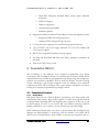
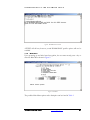
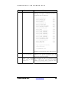
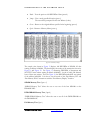
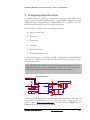
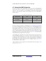
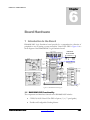
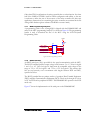
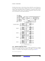
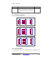
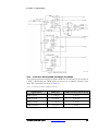
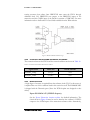
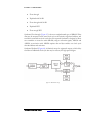
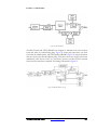
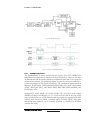
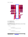
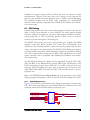
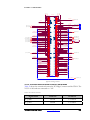
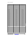
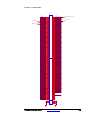
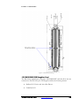
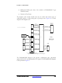
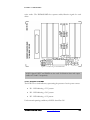
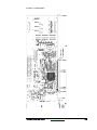
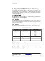
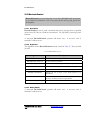
B O A R D
H A R D W A R E
•
Differential LVDS pairs (Note: Not available on DN6000K10SC Logic
Emulation board)
•
Headers for Test Points
The daughter card contains headers that may be useful with certain types of
oscilloscope probes, or when wiring pins to prototype areas. Figure 66 is a block
diagram of the daughter card.
DIFFERENTIAL
CONNECTOR
ACLK1
BCLK1
CCLK1
ECLK1
MBCK6
J5
DIFF CLOCK
J3, J4, J5, J6, J7- 50 PIN IDC HEADER
UNBUFFERED I/O 0..17
J2
DIFF PAIR A0..A15
J6
J7
UNBUFFERED I/O 0..23
50 PIN MINI D
RIBBON CABLE
CONNECTOR
UNBUFFERED I/O 0..23
LINEAR REGULATOR
12VDC TO 3.3V/
3.9VDC
POWER
INDICATORS
J1
BUFFERED I/O 0..15
U1
UNBUFFERED I/O 0..15
+3.3V +5.0V +12.0V
J3
BUFFERED I/O 0..7
U2
text
POWER
HEADER
UNBUFFERED I/O 0..15
BUFFERED I/O 0..7
+1.5V
+3.3V
+5.0V
+12.0V
-12.0V
J4
BUFFERED I/O 0..15
U3
UNBUFFERED I/O 0..15
J6
GND
74LVC16245APA/
74FST163245PA
200 PIN MICROPAX
(BOTTOM OF PWB)
20 PIN IDC
HEADER
U1, U2, U3 - BUFFERS OR LEVEL TRANSLATORS
Figure 66 - DN3000K10SD Daughter Card Block Diagram
The DN3000K10SD Daughter Card provides 16-differential pairs, 48-buffered
(passive/active) I/O, and 66-unbuffered I/O signals. The DN3000K10SD Daughter
Card is pictured in Figure 67.
DN6000K10SC User Guide
www.dinigroup.com
139