1
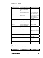
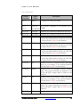
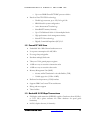
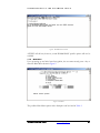
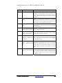
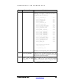
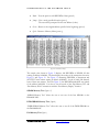
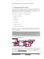
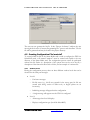
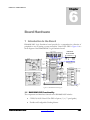
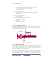
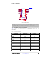
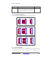
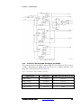
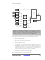
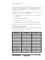
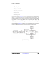
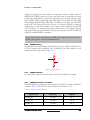
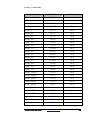
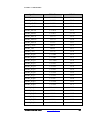
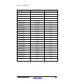
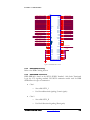
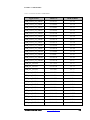
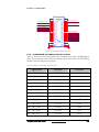
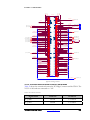
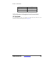
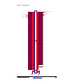
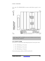
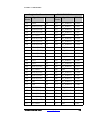
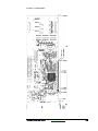
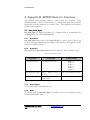
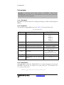
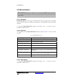
B O A R D
H A R D W A R E
+5V
-12V
+12V +5V
PCI_TDIO
P2
B1
B2
B3
B4
B5
B6
B7
B8
B9
B10
B11
PRSNT1
PRSNT2
Pg8 PCI_CLK
Pg6 PCI_REQn
PCI_CLK
PCI_REQn
VIO_2
PCI_AD31
PCI_AD29
PCI_AD27
PCI_AD25
V3_6
PCI_CBEn3
PCI_AD23
PCI_AD21
PCI_AD19
V3_5
PCI_AD17
PCI_CBEn2
Pg6 PCI_IRDYn
Pg6 PCI_DEVSELn
Pg6 PCI_LOCKn
Pg6 PCI_PERRn
Pg6 PCI_SERRn
PCI_IRDYn
V3_4
PCI_DEVSELn
PCIXCAP
PCI_LOCKn
PCI_PERRn
V3_3
PCI_SERRn
V3_2
PCI_CBEn1
PCI_AD14
PCI_AD12
PCI_AD10
PCI_M66EN
PCI_AD8
PCI_AD7
V3_1
PCI_AD5
PCI_AD3
PCI_AD1
VIO_3
Pg6 PCI_ACK64n
PCI_ACK64n
PCI_CBEn6
PCI_CBEn4
PCI_AD63
PCI_AD61
VIO_4
PCI_AD59
PCI_AD57
PCI_AD55
PCI_AD53
PCI_AD51
PCI_AD49
VIO_5
PCI_AD47
PCI_AD45
PCI_AD43
PCI_AD41
PCI_AD39
PCI_AD37
VIO_6
PCI_AD35
PCI_AD33
B14
B15
B16
B17
B18
B19
B20
B21
B22
B23
B24
B25
B26
B27
B28
B29
B30
B31
B32
B33
B34
B35
B36
B37
B38
B39
B40
B41
B42
B43
B44
B45
B46
B47
B48
B49
B50
B51
B52
B53
B54
B55
B56
B57
B58
B59
B60
B61
B62
B63
B64
B65
B66
B67
B68
B69
B70
B71
B72
B73
B74
B75
B76
B77
B78
B79
B80
B81
B82
B83
B84
B85
B86
B87
B88
B89
B90
B91
B92
B93
B94
-12V
TRST
TCK
+12V
GND
TMS
TDI
TDO
+5V
+5V
INTA
+5V
INTB
INTC
INTD
+5V
PRSNT1
RSVD
RSVD
+VIO
PRSNT2
RSVD
+3.3V Keyway
RSVD
GND
CLK
GND
REQ
+VIO
AD31
AD29
GND
AD27
AD25
+3.3V
C/BE3
AD23
GND
AD21
AD19
+3.3V
AD17
C/BE2
GND
IRDY
+3.3V
DEVSEL
PCIXCAP
LOCK
PERR
+3.3V
SERR
+3.3V
C/BE1
AD14
GND
AD12
AD10
M66EN
GND
GND
AD08
AD07
+3.3V
AD05
AD03
GND
AD01
+VIO
ACK64
+5V
+5V
64-bit
+3.3VAUX
RST
+VIO
GNT
GND
PME
AD30
+3.3V
AD28
AD26
GND
AD24
IDSEL
+3.3V
AD22
AD20
GND
AD18
AD16
+3.3V
FRAME
GND
TRDY
GND
STOP
+3.3V
SMBCLK
SMBDAT
GND
PAR
AD15
+3.3V
AD13
AD11
GND
AD09
GND
GND
C/BE0
+3.3V
AD06
AD04
GND
AD02
AD00
+VIO
REQ64
+5V
+5V
Keyway
RSVD
GND
C/BE6
C/BE4
GND
AD63
AD61
+VIO
AD59
AD57
GND
AD55
AD53
GND
AD51
AD49
+VIO
AD47
AD45
GND
AD43
AD41
GND
AD39
AD37
+VIO
AD35
AD33
GND
RSVD
RSVD
GND
GND
C/BE7
C/BE5
+VIO
PAR64
AD62
GND
AD60
AD58
GND
AD56
AD54
+VIO
AD52
AD50
GND
AD48
AD46
GND
AD44
AD42
+VIO
AD40
AD38
GND
AD36
AD34
GND
AD32
RSVD
GND
RSVD
A1
A2
A3
A4
A5
A6
A7
A8
A9
A10
A11
PCI_INTAn
PCI_INTAn Pg6
VIO_1
TP5
A14
A15
A16
A17
A18
A19
A20
A21
A22
A23
A24
A25
A26
A27
A28
A29
A30
A31
A32
A33
A34
A35
A36
A37
A38
A39
A40
A41
A42
A43
A44
A45
A46
A47
A48
A49
A50
A51
A52
A53
A54
A55
A56
A57
A58
A59
A60
A61
A62
A63
A64
A65
A66
A67
A68
A69
A70
A71
A72
A73
A74
A75
A76
A77
A78
A79
A80
A81
A82
A83
A84
A85
A86
A87
A88
A89
A90
A91
A92
A93
A94
+3.3VAUX
PCI_RSTn
VIO_2
PCI_GNTn
1
PCI_RSTn Pg6
PCI_GNTn Pg6
TP3
PMEn
1
PCI_AD30
V3_6
PCI_AD28
PCI_AD26
PCI_AD24
PCI_IDSEL
V3_5
PCI_IDSEL Pg6
PCI_AD22
PCI_AD20
PCI_AD18
PCI_AD16
V3_4
PCI_FRAMEn
PCI_TRDYn
PCI_STOPn
V3_3
R84
R85
PCI_PAR
PCI_AD15
PCI_FRAMEn Pg6
PCI_TRDYn Pg6
+3.3V
PCI_STOPn Pg6
5.1K
5.1K
PCI_PAR Pg6
V3_2
PCI_AD13
PCI_AD11
PCI_AD9
PCI_CBEn0
V3_1
PCI_AD6
PCI_AD4
PCI_AD2
PCI_AD0
VIO_3
PCI_REQ64n
PCI_REQ64n Pg6
PCI_CBEn7
PCI_CBEn5
VIO_4
PCI_PAR64
PCI_AD62
PCI_PAR64 Pg6
PCI_AD60
PCI_AD58
PCI_AD56
PCI_AD54
VIO_5
PCI_AD52
PCI_AD50
PCI_AD48
PCI_AD46
PCI_AD44
PCI_AD42
VIO_6
PCI_AD40
PCI_AD38
PCI_AD36
PCI_AD34
PCI_AD32
PCI64M_EDGE
PCI_AD[0..63]
PCI_AD[0..63]
Pg6
Figure 60 - PCI Edge Connector
10.1.3 Connection between the PCI connector and the FPGA
Table 30 shows the connection between the PCI Edge Connector and the FPGA. The
VCCO of the banks are connected to +3.0V.
Table 30 - PCI to FPGA Connections
Signal Name
Connector
FPGA Pin
PCI_AD0
P2.A58
U13.AF18
PCI_AD1
P2.B58
U13.AK19
DN6000K10SC User Guide
www.dinigroup.com
126