1
i960® Jx Microprocessor
Developer’s Manual
Release Date: December, 1997
Order Number: 272483-002
Information in this document is provided in connection with Intel products. No license, express or implied, by estoppel or
otherwise, to any intellectual property rights is granted by this document. Except as provided in Intel’s Terms and Conditions of
Sale for such products, Intel assumes no liability whatsoever, and Intel disclaims any express or implied warranty, relating to sale
and/or use of Intel products including liability or warranties relating to fitness for a particular purpose, merchantability, or
infringement of any patent, copyright or other intellectual property right. Intel products are not intended for use in medical, life
saving, or life sustaining applications.
Intel may make changes to specifications and product descriptions at any time, without notice.
Designers must not rely on the absence or characteristics of any features or instructions marked "reserved" or "undefined." Intel
reserves these for future definition and shall have no responsibility whatsoever for conflicts or incompatibilities arising from future
changes to them.
The i960® Jx Processor may contain design defects or errors known as errata which may cause the product to deviate from
published specifications. Current characterized errata are available on request.
Contact your local Intel sales office or your distributor to obtain the latest specifications and before placing your product order.
Copies of documents which have an ordering number and are referenced in this document, or other Intel literature may be
obtained by calling 1-800-548-4725 or by visiting Intel’s website at http://www.intel.com.
Copyright © Intel Corporation, 1997
*Third-party brands and names are the property of their respective owners.
ii
May, 1998
272483-002
i960® Jx Microprocessor
Developer’s Manual
CHAPTER 1
INTRODUCTION
1.1
Product Features........................................................................................................... 1-4
1.1.1
Instruction Cache .................................................................................................... 1-4
1.1.2
Data Cache ............................................................................................................. 1-4
1.1.3
On-chip (Internal) Data RAM ................................................................................... 1-4
1.1.4
Local Register Cache .............................................................................................. 1-5
1.1.5
Interrupt Controller .................................................................................................. 1-5
1.1.6
Timer Support .......................................................................................................... 1-6
1.1.7
Memory-Mapped Control Registers (MMR) ............................................................. 1-6
1.1.8
External Bus ............................................................................................................ 1-6
1.1.9
Complete Fault Handling and Debug Capabilities ................................................... 1-7
1.2
ABOUT THIS MANUAL................................................................................................. 1-7
1.3
NOTATION AND TERMINOLOGY................................................................................ 1-8
1.3.1
Reserved and Preserved ......................................................................................... 1-8
1.3.2
Specifying Bit and Signal Values ............................................................................. 1-9
1.3.3
Representing Numbers ........................................................................................... 1-9
1.3.4
Register Names ....................................................................................................... 1-9
1.4
Related Documents..................................................................................................... 1-10
CHAPTER 2
DATA TYPES AND MEMORY ADDRESSING MODES
2.1
DATA TYPES ................................................................................................................
2.1.1
Integers ...................................................................................................................
2.1.2
Ordinals ...................................................................................................................
2.1.3
Bits and Bit Fields ....................................................................................................
2.1.4
Triple- and Quad-Words ..........................................................................................
2.1.5
Register Data Alignment .........................................................................................
2.1.6
Literals .....................................................................................................................
2.2
BIT AND BYTE ORDERING IN MEMORY....................................................................
2.2.1
Bit Ordering .............................................................................................................
2.2.2
Byte Ordering ..........................................................................................................
2.3
MEMORY ADDRESSING MODES ...............................................................................
2.3.1
Absolute ..................................................................................................................
2.3.2
Register Indirect ......................................................................................................
2.3.3
Index with Displacement .........................................................................................
2.3.4
IP with Displacement ...............................................................................................
2.3.5
Addressing Mode Examples ....................................................................................
2-1
2-2
2-2
2-3
2-3
2-3
2-4
2-4
2-4
2-4
2-6
2-7
2-7
2-8
2-8
2-8
iii
CHAPTER 3
PROGRAMMING ENVIRONMENT
3.1
OVERVIEW ................................................................................................................... 3-1
3.2
REGISTERS AND LITERALS AS INSTRUCTION OPERANDS................................... 3-1
3.2.1
Global Registers ...................................................................................................... 3-2
3.2.2
Local Registers ........................................................................................................ 3-3
3.2.3
Register Scoreboarding ........................................................................................... 3-4
3.2.4
Literals ..................................................................................................................... 3-4
3.2.5
Register and Literal Addressing and Alignment ....................................................... 3-4
3.3
MEMORY-MAPPED CONTROL REGISTERS.............................................................. 3-6
3.3.1
Memory-Mapped Registers (MMR) ......................................................................... 3-6
3.3.1.1
Restrictions on Instructions that Access Memory-Mapped Registers .............. 3-6
3.3.1.2
Access Faults ................................................................................................... 3-7
3.4
ARCHITECTURALLY DEFINED DATA STRUCTURES ............................................. 3-11
3.5
MEMORY ADDRESS SPACE..................................................................................... 3-13
3.5.1
Memory Requirements .......................................................................................... 3-14
3.5.2
Data and Instruction Alignment in the Address Space .......................................... 3-15
3.5.3
Byte, Word and Bit Addressing .............................................................................. 3-15
3.5.4
Internal Data RAM ................................................................................................. 3-16
3.5.5
Instruction Cache ................................................................................................... 3-16
3.5.6
Data Cache ............................................................................................................ 3-17
3.6
LOCAL REGISTER CACHE........................................................................................ 3-17
3.7
PROCESSOR-STATE REGISTERS ........................................................................... 3-17
3.7.1
Instruction Pointer (IP) Register ............................................................................ 3-17
3.7.2
Arithmetic Controls (AC) Register .......................................................................... 3-18
3.7.2.1
Initializing and Modifying the AC Register ...................................................... 3-18
3.7.2.2
Condition Code (AC.cc) .................................................................................. 3-19
3.7.3
Process Controls (PC) Register ............................................................................. 3-21
3.7.3.1
Initializing and Modifying the PC Register ...................................................... 3-22
3.7.4
Trace Controls (TC) Register ................................................................................. 3-23
3.8
USER-SUPERVISOR PROTECTION MODEL ........................................................... 3-23
3.8.1
Supervisor Mode Resources ................................................................................. 3-23
3.8.2
Using the User-Supervisor Protection Model ......................................................... 3-24
CHAPTER 4
CACHE AND ON-CHIP DATA RAM
4.1
INTERNAL DATA RAM .................................................................................................
4.2
LOCAL REGISTER CACHE..........................................................................................
4.3
BIG ENDIAN ACCESSES TO INTERNAL RAM AND DATA CACHE...........................
4.4
INSTRUCTION CACHE ................................................................................................
4.4.1
Enabling and Disabling the Instruction Cache .........................................................
4.4.2
Operation While the Instruction Cache Is Disabled .................................................
4.4.3
Loading and Locking Instructions in the Instruction Cache .....................................
iv
4-1
4-2
4-4
4-4
4-4
4-5
4-5
4.4.4
4.4.5
4.5
4.5.1
4.5.2
4.5.3
4.5.4
4.5.5
4.5.6
4.5.7
Instruction Cache Visibility ...................................................................................... 4-5
Instruction Cache Coherency .................................................................................. 4-5
DATA CACHE ............................................................................................................... 4-6
Enabling and Disabling the Data Cache .................................................................. 4-6
Multi-Word Data Accesses that Partially Hit the Data Cache .................................. 4-7
Data Cache Fill Policy ............................................................................................. 4-8
Data Cache Write Policy ......................................................................................... 4-8
Data Cache Coherency and Non-Cacheable Accesses .......................................... 4-9
External I/O and Bus Masters and Cache Coherency ........................................... 4-10
Data Cache Visibility ............................................................................................. 4-10
CHAPTER 5
INSTRUCTION SET OVERVIEW
5.1
INSTRUCTION FORMATS ........................................................................................... 5-1
5.1.1
Assembly Language Format ................................................................................... 5-1
5.1.2
Instruction Encoding Formats .................................................................................. 5-2
5.1.3
Instruction Operands ............................................................................................... 5-3
5.2
INSTRUCTION GROUPS ............................................................................................. 5-4
5.2.1
Data Movement ....................................................................................................... 5-5
5.2.1.1
Load and Store Instructions ............................................................................. 5-5
5.2.1.2
Move ................................................................................................................ 5-6
5.2.1.3
Load Address ................................................................................................... 5-6
5.2.2
Select Conditional ................................................................................................... 5-6
5.2.3
Arithmetic ................................................................................................................ 5-7
5.2.3.1
Add, Subtract, Multiply, Divide, Conditional Add, Conditional Subtract ............ 5-8
5.2.3.2
Remainder and Modulo .................................................................................... 5-8
5.2.3.3
Shift, Rotate and Extended Shift ...................................................................... 5-9
5.2.3.4
Extended Arithmetic ....................................................................................... 5-10
5.2.4
Logical ................................................................................................................... 5-10
5.2.5
Bit, Bit Field and Byte Operations ......................................................................... 5-11
5.2.5.1
Bit Operations ................................................................................................ 5-11
5.2.5.2
Bit Field Operations ........................................................................................ 5-11
5.2.5.3
Byte Operations ............................................................................................. 5-11
5.2.6
Comparison ........................................................................................................... 5-12
5.2.6.1
Compare and Conditional Compare ............................................................... 5-12
5.2.6.2
Compare and Increment or Decrement .......................................................... 5-13
5.2.6.3
Test Condition Codes ..................................................................................... 5-13
5.2.7
Branch ................................................................................................................... 5-14
5.2.7.1
Unconditional Branch ..................................................................................... 5-14
5.2.7.2
Conditional Branch ......................................................................................... 5-15
5.2.7.3
Compare and Branch ..................................................................................... 5-15
5.2.8
Call/Return ............................................................................................................ 5-16
5.2.9
Faults ..................................................................................................................... 5-17
5.2.10
Debug .................................................................................................................... 5-18
5.2.11
Atomic Instructions ................................................................................................ 5-18
v
5.2.12
Processor Management ........................................................................................
5.3
PERFORMANCE OPTIMIZATION ..............................................................................
5.3.1
Instruction Optimizations .......................................................................................
5.3.1.1
Load / Store Execution Model ........................................................................
5.3.1.2
Compare Operations ......................................................................................
5.3.1.3
Microcoded Instructions .................................................................................
5.3.1.4
Multiply-Divide Unit Instructions .....................................................................
5.3.1.5
Multi-Cycle Register Operations .....................................................................
5.3.1.6
Simple Control Transfer .................................................................................
5.3.1.7
Memory Instructions .......................................................................................
5.3.1.8
Unaligned Memory Accesses .........................................................................
5.3.2
Miscellaneous Optimizations .................................................................................
5.3.2.1
Masking of Integer Overflow ...........................................................................
5.3.2.2
Avoid Using PFP, SP, R3 As Destinations for MDU Instructions ...................
5.3.2.3
Use Global Registers (g0 - g14) As Destinations for MDU Instructions .........
5.3.2.4
Execute in Imprecise Fault Mode ...................................................................
5-19
5-20
5-20
5-20
5-20
5-21
5-21
5-21
5-22
5-22
5-23
5-23
5-23
5-23
5-23
5-24
CHAPTER 6
INSTRUCTION SET REFERENCE
6.1
NOTATION .................................................................................................................... 6-1
6.1.1
Alphabetic Reference .............................................................................................. 6-2
6.1.2
Mnemonic ................................................................................................................ 6-2
6.1.3
Format ..................................................................................................................... 6-2
6.1.4
Description ............................................................................................................... 6-3
6.1.5
Action ....................................................................................................................... 6-3
6.1.6
Faults ....................................................................................................................... 6-5
6.1.7
Example ................................................................................................................... 6-5
6.1.8
Opcode and Instruction Format ............................................................................... 6-6
6.1.9
See Also .................................................................................................................. 6-6
6.1.10
Side Effects ............................................................................................................. 6-6
6.1.11
Notes ....................................................................................................................... 6-6
6.2
INSTRUCTIONS............................................................................................................ 6-6
6.2.1
ADD<cc> ................................................................................................................. 6-7
6.2.2
addc ....................................................................................................................... 6-10
6.2.3
addi, addo .............................................................................................................. 6-11
6.2.4
alterbit .................................................................................................................... 6-12
6.2.5
and, andnot ............................................................................................................ 6-13
6.2.6
atadd ...................................................................................................................... 6-14
6.2.7
atmod ..................................................................................................................... 6-15
6.2.8
b, bx ....................................................................................................................... 6-16
6.2.9
bal, balx ................................................................................................................. 6-17
6.2.10
bbc, bbs ................................................................................................................. 6-19
6.2.11
BRANCH<cc> ........................................................................................................ 6-21
6.2.12
bswap .................................................................................................................... 6-23
6.2.13
call ......................................................................................................................... 6-24
vi
6.2.14
6.2.15
6.2.16
6.2.17
6.2.18
6.2.19
6.2.20
6.2.21
6.2.22
6.2.23
6.2.24
6.2.25
6.2.26
6.2.27
6.2.28
6.2.29
6.2.30
6.2.31
6.2.32
6.2.33
6.2.34
6.2.35
6.2.36
6.2.37
6.2.38
6.2.39
6.2.40
6.2.41
6.2.42
6.2.43
6.2.44
6.2.45
6.2.46
6.2.47
6.2.48
6.2.49
6.2.50
6.2.51
6.2.52
6.2.53
6.2.54
6.2.55
6.2.56
6.2.57
calls .......................................................................................................................
callx .......................................................................................................................
chkbit .....................................................................................................................
clrbit .......................................................................................................................
cmpdeci, cmpdeco ................................................................................................
cmpinci, cmpinco ...................................................................................................
COMPARE ............................................................................................................
COMPARE AND BRANCH<cc> ............................................................................
concmpi, concmpo ................................................................................................
dcctl .......................................................................................................................
divi, divo ................................................................................................................
ediv ........................................................................................................................
emul .......................................................................................................................
eshro .....................................................................................................................
extract ....................................................................................................................
FAULT<cc> ...........................................................................................................
flushreg ..................................................................................................................
fmark .....................................................................................................................
halt .........................................................................................................................
icctl ........................................................................................................................
intctl .......................................................................................................................
intdis ......................................................................................................................
inten .......................................................................................................................
LOAD .....................................................................................................................
lda ..........................................................................................................................
mark ......................................................................................................................
modac ....................................................................................................................
modi .......................................................................................................................
modify ....................................................................................................................
modpc ....................................................................................................................
modtc .....................................................................................................................
MOVE ....................................................................................................................
muli, mulo ..............................................................................................................
nand ......................................................................................................................
nor .........................................................................................................................
not, notand ............................................................................................................
notbit ......................................................................................................................
notor ......................................................................................................................
or, ornot .................................................................................................................
remi, remo .............................................................................................................
ret ..........................................................................................................................
rotate .....................................................................................................................
scanbit ...................................................................................................................
scanbyte ................................................................................................................
6-25
6-27
6-29
6-30
6-31
6-32
6-33
6-35
6-38
6-40
6-47
6-48
6-49
6-50
6-51
6-52
6-54
6-55
6-56
6-58
6-66
6-68
6-69
6-70
6-73
6-74
6-75
6-76
6-77
6-78
6-80
6-81
6-84
6-85
6-86
6-87
6-88
6-89
6-90
6-91
6-92
6-94
6-95
6-96
vii
6.2.58
6.2.59
6.2.60
6.2.61
6.2.62
6.2.63
6.2.64
6.2.65
6.2.66
6.2.67
6.2.68
6.2.69
SEL<cc> ................................................................................................................ 6-97
setbit ...................................................................................................................... 6-99
SHIFT .................................................................................................................. 6-100
spanbit ................................................................................................................. 6-103
STORE ................................................................................................................ 6-104
subc ..................................................................................................................... 6-108
SUB<cc> ............................................................................................................. 6-109
subi, subo ............................................................................................................ 6-112
syncf .................................................................................................................... 6-113
sysctl .................................................................................................................... 6-114
TEST<cc> ............................................................................................................ 6-118
xnor, xor ............................................................................................................... 6-120
CHAPTER 7
PROCEDURE CALLS
7.1
CALL AND RETURN MECHANISM .............................................................................. 7-2
7.1.1
Local Registers and the Procedure Stack ............................................................... 7-2
7.1.2
Local Register and Stack Management ................................................................... 7-4
7.1.2.1
Frame Pointer ................................................................................................... 7-4
7.1.2.2
Stack Pointer .................................................................................................... 7-4
7.1.2.3
Considerations When Pushing Data onto the Stack ........................................ 7-4
7.1.2.4
Considerations When Popping Data off the Stack ........................................... 7-5
7.1.2.5
Previous Frame Pointer .................................................................................... 7-5
7.1.2.6
Return Type Field ............................................................................................. 7-5
7.1.2.7
Return Instruction Pointer ................................................................................. 7-5
7.1.3
Call and Return Action ............................................................................................. 7-5
7.1.3.1
Call Operation .................................................................................................. 7-6
7.1.3.2
Return Operation .............................................................................................. 7-7
7.1.4
Caching Local Register Sets ................................................................................... 7-7
7.1.4.1
Reserving Local Register Sets for High Priority Interrupts ............................... 7-8
7.1.5
Mapping Local Registers to the Procedure Stack .................................................. 7-11
7.2
MODIFYING THE PFP REGISTER............................................................................. 7-11
7.3
PARAMETER PASSING ............................................................................................. 7-12
7.4
LOCAL CALLS ............................................................................................................ 7-14
7.5
SYSTEM CALLS ......................................................................................................... 7-15
7.5.1
System Procedure Table ....................................................................................... 7-15
7.5.1.1
Procedure Entries ........................................................................................... 7-17
7.5.1.2
Supervisor Stack Pointer ................................................................................ 7-17
7.5.1.3
Trace Control Bit ............................................................................................ 7-17
7.5.2
System Call to a Local Procedure ......................................................................... 7-18
7.5.3
System Call to a Supervisor Procedure ................................................................. 7-18
7.6
USER AND SUPERVISOR STACKS .......................................................................... 7-19
7.7
INTERRUPT AND FAULT CALLS............................................................................... 7-19
7.8
RETURNS ................................................................................................................... 7-20
viii
7.9
BRANCH-AND-LINK ................................................................................................... 7-21
CHAPTER 8
FAULTS
8.1
FAULT HANDLING OVERVIEW ................................................................................... 8-1
8.2
FAULT TYPES .............................................................................................................. 8-3
8.3
FAULT TABLE .............................................................................................................. 8-4
8.4
STACK USED IN FAULT HANDLING........................................................................... 8-6
8.5
FAULT RECORD .......................................................................................................... 8-6
8.5.1
Fault Record Description ......................................................................................... 8-7
8.5.2
Fault Record Location ............................................................................................. 8-8
8.6
MULTIPLE AND PARALLEL FAULTS .......................................................................... 8-9
8.6.1
Multiple Non-Trace Faults on the Same Instruction ................................................ 8-9
8.6.2
Multiple Trace Fault Conditions on the Same Instruction ........................................ 8-9
8.6.3
Multiple Trace and Non-Trace Fault Conditions on the Same Instruction ............... 8-9
8.6.4
Parallel Faults .......................................................................................................... 8-9
8.6.4.1
Faults on Multiple Instructions Executed in Parallel ....................................... 8-10
8.6.4.2
Fault Record for Parallel Faults ...................................................................... 8-11
8.6.5
Override Faults ...................................................................................................... 8-11
8.6.6
System Error ......................................................................................................... 8-12
8.7
FAULT HANDLING PROCEDURES ........................................................................... 8-12
8.7.1
Possible Fault Handling Procedure Actions .......................................................... 8-13
8.7.2
Program Resumption Following a Fault ................................................................ 8-13
8.7.2.1
Faults Happening Before Instruction Execution ............................................. 8-13
8.7.2.2
Faults Happening During Instruction Execution ............................................. 8-14
8.7.2.3
Faults Happening After Instruction Execution ................................................ 8-14
8.7.3
Return Instruction Pointer (RIP) ............................................................................ 8-14
8.7.4
Returning to the Point in the Program Where the Fault Occurred ......................... 8-15
8.7.5
Returning to a Point in the Program Other Than Where the Fault Occurred ......... 8-15
8.7.6
Fault Controls ........................................................................................................ 8-15
8.8
FAULT HANDLING ACTION....................................................................................... 8-16
8.8.1
Local Fault Call ...................................................................................................... 8-17
8.8.2
System-Local Fault Call ........................................................................................ 8-17
8.8.3
System-Supervisor Fault Call ................................................................................ 8-17
8.8.4
Faults and Interrupts ............................................................................................. 8-18
8.9
PRECISE AND IMPRECISE FAULTS ........................................................................ 8-19
8.9.1
Precise Faults ........................................................................................................ 8-19
8.9.2
Imprecise Faults .................................................................................................... 8-19
8.9.3
Asynchronous Faults ............................................................................................. 8-19
8.9.4
No Imprecise Faults (AC.nif) Bit ............................................................................ 8-20
8.9.5
Controlling Fault Precision .................................................................................... 8-20
8.10
FAULT REFERENCE.................................................................................................. 8-21
8.10.1
ARITHMETIC Faults .............................................................................................. 8-22
8.10.2
CONSTRAINT Faults ............................................................................................ 8-23
ix
8.10.3
8.10.4
8.10.5
8.10.6
8.10.7
8.10.8
OPERATION Faults ...............................................................................................
OVERRIDE Faults .................................................................................................
PARALLEL Faults ..................................................................................................
PROTECTION Faults ............................................................................................
TRACE Faults ........................................................................................................
TYPE Faults ..........................................................................................................
8-24
8-26
8-27
8-28
8-29
8-32
CHAPTER 9
TRACING AND DEBUGGING
9.1
TRACE CONTROLS ..................................................................................................... 9-1
9.1.1
Trace Controls (TC) Register ................................................................................... 9-2
9.1.2
PC Trace Enable Bit and Trace-Fault-Pending Flag ............................................... 9-3
9.2
TRACE MODES ............................................................................................................ 9-3
9.2.1
Instruction Trace ...................................................................................................... 9-3
9.2.2
Branch Trace ........................................................................................................... 9-4
9.2.3
Call Trace ................................................................................................................ 9-4
9.2.4
Return Trace ............................................................................................................ 9-4
9.2.5
Prereturn Trace ....................................................................................................... 9-4
9.2.6
Supervisor Trace ..................................................................................................... 9-5
9.2.7
Mark Trace .............................................................................................................. 9-5
9.2.7.1
Software Breakpoints ....................................................................................... 9-5
9.2.7.2
Hardware Breakpoints ...................................................................................... 9-5
9.2.7.3
Requesting Modification Rights to Hardware Breakpoint Resources ............... 9-6
9.2.7.4
Breakpoint Control Register ............................................................................. 9-7
9.2.7.5
Data Address Breakpoint (DAB) Registers ....................................................... 9-9
9.2.7.6
Instruction Breakpoint (IPB) Registers ........................................................... 9-10
9.3
GENERATING A TRACE FAULT................................................................................ 9-11
9.4
HANDLING MULTIPLE TRACE EVENTS................................................................... 9-11
9.5
TRACE FAULT HANDLING PROCEDURE ................................................................ 9-12
9.5.1
Tracing and Interrupt Procedures .......................................................................... 9-12
9.5.2
Tracing on Calls and Returns ................................................................................ 9-12
9.5.2.1
Tracing on Explicit Call ................................................................................... 9-13
9.5.2.2
Tracing on Implicit Call ................................................................................... 9-14
9.5.2.3
Tracing on Return from Explicit Call ............................................................... 9-15
9.5.2.4
Tracing on Return from Implicit Call: Fault Case ............................................ 9-15
9.5.2.5
Tracing on Return from Implicit Call: Interrupt Case ...................................... 9-16
CHAPTER 10
TIMERS
10.1
TIMER REGISTERS....................................................................................................
10.1.1
Timer Mode Registers (TMR0, TMR1) ..................................................................
10.1.1.1
Bit 0 - Terminal Count Status Bit (TMRx.tc) ...................................................
10.1.1.2
Bit 1 - Timer Enable (TMRx.enable) ...............................................................
10.1.1.3
Bit 2 - Timer Auto Reload Enable (TMRx.reload) ...........................................
10.1.1.4
Bit 3 - Timer Register Supervisor Read/Write Control (TMRx.sup) ................
x
10-2
10-3
10-4
10-4
10-5
10-5
10.1.1.5
Bits 4, 5 - Timer Input Clock Select (TMRx.csel1:0) ....................................... 10-6
10.1.2
Timer Count Register (TCR0, TCR1) .................................................................... 10-6
10.1.3
Timer Reload Register (TRR0, TRR1) .................................................................. 10-7
10.2
TIMER OPERATION ................................................................................................... 10-7
10.2.1
Basic Timer Operation ........................................................................................... 10-7
10.2.2
Load/Store Access Latency for Timer Registers ................................................... 10-9
10.3
TIMER INTERRUPTS ............................................................................................... 10-11
10.4
POWERUP/RESET INITIALIZATION ....................................................................... 10-11
10.5
UNCOMMON TCRX AND TRRX CONDITIONS....................................................... 10-12
10.6
TIMER STATE DIAGRAM......................................................................................... 10-13
CHAPTER 11
INTERRUPTS
11.1
OVERVIEW ................................................................................................................. 11-1
11.1.1
The i960® Jx Processor Interrupt Controller .......................................................... 11-2
11.2
SOFTWARE REQUIREMENTS FOR INTERRUPT HANDLING ................................ 11-3
11.3
INTERRUPT PRIORITY.............................................................................................. 11-3
11.4
INTERRUPT TABLE ................................................................................................... 11-4
11.4.1
Vector Entries ........................................................................................................ 11-5
11.4.2
Pending Interrupts ................................................................................................. 11-5
11.4.3
Caching Portions of the Interrupt Table ................................................................. 11-6
11.5
INTERRUPT STACK AND INTERRUPT RECORD .................................................... 11-7
11.6
MANAGING INTERRUPT REQUESTS ...................................................................... 11-8
11.6.1
External Interrupts ................................................................................................. 11-8
11.6.2
Non-Maskable Interrupt (NMI) ............................................................................... 11-8
11.6.3
Timer Interrupts ..................................................................................................... 11-9
11.6.4
Software Interrupts ................................................................................................ 11-9
11.6.5
Posting Interrupts .................................................................................................. 11-9
11.6.5.1
Posting Software Interrupts via sysctl ............................................................ 11-9
11.6.5.2
Posting Software Interrupts Directly in the Interrupt Table ........................... 11-11
11.6.5.3
Posting External Interrupts ........................................................................... 11-11
11.6.5.4
Posting Hardware Interrupts ........................................................................ 11-11
11.6.6
Resolving Interrupt Priority .................................................................................. 11-11
11.6.7
Sampling Pending Interrupts in the Interrupt Table ............................................. 11-12
11.6.8
Interrupt Controller Modes ................................................................................... 11-14
11.6.8.1
Dedicated Mode ........................................................................................... 11-14
11.6.8.2
Expanded Mode ........................................................................................... 11-15
11.6.8.3
Mixed Mode .................................................................................................. 11-17
11.6.9
Saving the Interrupt Mask ................................................................................... 11-17
11.7
EXTERNAL INTERFACE DESCRIPTION ................................................................ 11-18
11.7.1
Pin Descriptions .................................................................................................. 11-18
11.7.2
Interrupt Detection Options ................................................................................. 11-19
11.7.3
Memory-Mapped Control Registers ..................................................................... 11-21
11.7.4
Interrupt Control Register (ICON) ........................................................................ 11-22
xi
11.7.5
Interrupt Mapping Registers (IMAP0-IMAP2) ......................................................
11.7.5.1
Interrupt Mask (IMSK) and Interrupt Pending (IPND) Registers ...................
11.7.5.2
Interrupt Controller Register Access Requirements .....................................
11.7.5.3
Default and Reset Register Values ..............................................................
11.8
INTERRUPT OPERATION SEQUENCE...................................................................
11.8.1
Setting Up the Interrupt Controller .......................................................................
11.8.2
Interrupt Service Routines ...................................................................................
11.8.3
Interrupt Context Switch ......................................................................................
11.8.3.1
Servicing an Interrupt from Executing State .................................................
11.8.3.2
Servicing an Interrupt from Interrupted State ...............................................
11.9
OPTIMIZING INTERRUPT PERFORMANCE ...........................................................
11.9.1
Interrupt Service Latency .....................................................................................
11.9.2
Features to Improve Interrupt Performance .........................................................
11.9.2.1
Vector Caching Option .................................................................................
11.9.2.2
Caching Interrupt Routines and Reserving Register Frames .......................
11.9.2.3
Caching the Interrupt Stack ..........................................................................
11.9.3
Base Interrupt Latency ........................................................................................
11.9.4
Maximum Interrupt Latency .................................................................................
11.9.4.1
Avoiding Certain Destinations for MDU Operations .....................................
11.9.4.2
Masking Integer Overflow Faults for syncf ...................................................
11-23
11-25
11-27
11-28
11-28
11-31
11-31
11-32
11-32
11-33
11-33
11-35
11-35
11-35
11-36
11-36
11-37
11-38
11-42
11-42
CHAPTER 12
INITIALIZATION AND SYSTEM REQUIREMENTS
12.1
OVERVIEW ................................................................................................................. 12-1
12.2
INITIALIZATION .......................................................................................................... 12-2
12.2.1
Reset State Operation ........................................................................................... 12-3
12.2.2
Self Test Function (STEST, FAIL) ......................................................................... 12-6
12.2.2.1
The STEST Pin .............................................................................................. 12-7
12.2.2.2
External Bus Confidence Test ........................................................................ 12-7
12.2.2.3
The Fail Pin (FAIL) ......................................................................................... 12-7
12.2.2.4
IMI Alignment Check and System Error ......................................................... 12-8
12.2.2.5
FAIL Code ...................................................................................................... 12-8
12.3
Architecturally Reserved Memory Space .................................................................... 12-9
12.3.1
Initial Memory Image (IMI) ................................................................................... 12-10
12.3.1.1
Initialization Boot Record (IBR) .................................................................... 12-13
12.3.1.2
Process Control Block (PRCB) ..................................................................... 12-16
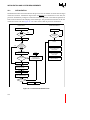
12.3.2
Process PRCB Flow ............................................................................................ 12-18
12.3.2.1
AC Initial Image ............................................................................................ 12-19
12.3.2.2
Fault Configuration Word ............................................................................. 12-19
12.3.2.3
Instruction Cache Configuration Word ......................................................... 12-19
12.3.2.4
Register Cache Configuration Word ............................................................. 12-19
12.3.3
Control Table ....................................................................................................... 12-20
12.4
DEVICE IDENTIFICATION ON RESET .................................................................... 12-22
12.4.1
Reinitializing and Relocating Data Structures ...................................................... 12-22
12.5
Startup Code Example .............................................................................................. 12-23
xii
12.6
SYSTEM REQUIREMENTS......................................................................................
12.6.1
Input Clock (CLKIN) ............................................................................................
12.6.2
Power and Ground Requirements (VCC, VSS) .....................................................
12.6.3
VCC5 Pin Requirements .......................................................................................
12.6.4
Power and Ground Planes ..................................................................................
12.6.5
Decoupling Capacitors ........................................................................................
12.6.6
I/O Pin Characteristics .........................................................................................
12.6.6.1
Output Pins ..................................................................................................
12.6.6.2
Input Pins .....................................................................................................
12.6.7
High Frequency Design Considerations ..............................................................
12.6.8
Line Termination ..................................................................................................
12.6.9
Latchup ................................................................................................................
12.6.10
Interference .........................................................................................................
12-34
12-34
12-34
12-35
12-35
12-36
12-36
12-37
12-37
12-38
12-38
12-39
12-40
CHAPTER 13
MEMORY CONFIGURATION
13.1
Memory Attributes ....................................................................................................... 13-1
13.1.1
Physical Memory Attributes ................................................................................... 13-1
13.1.2
Logical Memory Attributes ..................................................................................... 13-2
13.2
Differences With Previous i960 Processors ................................................................ 13-3
13.3
Programming the Physical Memory Attributes (PMCON Registers) ........................... 13-4
13.3.1
Bus Width .............................................................................................................. 13-5
13.4
Physical Memory Attributes at Initialization ................................................................. 13-5
13.4.1
Bus Control (BCON) Register ................................................................................ 13-6
13.5
Boundary Conditions for Physical Memory Regions ................................................... 13-7
13.5.1
Internal Memory Locations .................................................................................... 13-7
13.5.2
Bus Transactions Across Region Boundaries ....................................................... 13-7
13.5.3
Modifying the PMCON Registers ........................................................................... 13-7
13.6
Programming the Logical Memory Attributes .............................................................. 13-8
13.6.1
Defining the Effective Range of a Logical Data Template ................................... 13-11
13.6.2
Selecting the Byte Order ..................................................................................... 13-12
13.6.3
Data Caching Enable .......................................................................................... 13-12
13.6.4
Enabling the Logical Memory Template .............................................................. 13-12
13.6.5
Initialization .......................................................................................................... 13-13
13.6.6
Boundary Conditions for Logical Memory Templates .......................................... 13-13
13.6.6.1
Internal Memory Locations ........................................................................... 13-13
13.6.6.2
Overlapping Logical Data Template Ranges ............................................... 13-13
13.6.6.3
Accesses Across LMT Boundaries .............................................................. 13-14
13.6.7
Modifying the LMT Registers ............................................................................... 13-14
13.6.8
Dynamic Byte Order Changing ............................................................................ 13-14
CHAPTER 14
EXTERNAL BUS
14.1
OVERVIEW ................................................................................................................. 14-1
xiii
14.2
BUS OPERATION ....................................................................................................... 14-1
14.2.1
Basic Bus States ................................................................................................... 14-2
14.2.2
Bus Signal Types ................................................................................................... 14-4
14.2.2.1
Clock Signal ................................................................................................... 14-4
14.2.2.2
Address/Data Signal Definitions ..................................................................... 14-4
14.2.2.3
Control/Status Signal Definitions .................................................................... 14-4
14.2.3
Bus Accesses ........................................................................................................ 14-6
14.2.3.1
Bus Width ....................................................................................................... 14-7
14.2.3.2
Basic Bus Accesses ....................................................................................... 14-9
14.2.3.3
Burst Transactions ....................................................................................... 14-11
14.2.3.4
Wait States ................................................................................................... 14-17
14.2.3.5
Recovery States ........................................................................................... 14-19
14.2.4
Bus and Control Signals During Recovery and Idle States ................................. 14-22
14.2.5
Data Alignment .................................................................................................... 14-22
14.2.6
Byte Ordering and Bus Accesses ........................................................................ 14-28
14.2.7
Atomic Bus Transactions ..................................................................................... 14-30
14.2.8
Bus Arbitration ..................................................................................................... 14-31
14.2.8.1
HOLD/HOLDA Protocol ................................................................................ 14-32
14.2.8.2
BSTAT Signal ............................................................................................... 14-33
14.3
BUS APPLICATIONS ................................................................................................ 14-34
14.3.1
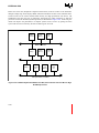
System Block Diagrams ...................................................................................... 14-34
14.3.1.1
Memory Subsystems .................................................................................... 14-37
14.3.1.2
I/O Subsystems ............................................................................................ 14-37
CHAPTER 15
TEST FEATURES
15.1
ON-CIRCUIT EMULATION (ONCE)............................................................................ 15-1
15.1.1
Entering/Exiting ONCE Mode ................................................................................ 15-1
15.2
BOUNDARY SCAN (JTAG)......................................................................................... 15-2
15.2.1
Boundary Scan Architecture .................................................................................. 15-2
15.2.1.1
TAP Controller ................................................................................................ 15-2
15.2.1.2
Instruction Register ........................................................................................ 15-2
15.2.1.3
Test Data Registers ........................................................................................ 15-2
15.2.1.4
TAP Elements ................................................................................................ 15-3
15.3
TAP REGISTERS........................................................................................................ 15-5
15.3.1
Instruction Register (IR) ......................................................................................... 15-5
15.3.2
TAP Test Data Registers ....................................................................................... 15-6
15.3.2.1
Device Identification Register ......................................................................... 15-6
15.3.2.2
Bypass Register ............................................................................................. 15-6
15.3.2.3
RUNBIST Register ......................................................................................... 15-7
15.3.2.4
Boundary-Scan Register ................................................................................ 15-7
15.3.3
Boundary Scan Instruction Set .............................................................................. 15-8
15.3.4
IEEE Required Instructions ................................................................................... 15-8
15.3.5
TAP Controller ....................................................................................................... 15-9
15.3.5.1
Test Logic Reset State ................................................................................. 15-10
15.3.5.2
Run-Test/Idle State ...................................................................................... 15-10
xiv
15.3.5.3
Select-DR-Scan State ..................................................................................
15.3.5.4
Capture-DR State .........................................................................................
15.3.5.5
Shift-DR State ..............................................................................................
15.3.5.6
Exit1-DR State .............................................................................................
15.3.5.7
Pause-DR State ...........................................................................................
15.3.5.8
Exit2-DR State .............................................................................................
15.3.5.9
Update-DR State ..........................................................................................
15.3.5.10
Select-IR Scan State ....................................................................................
15.3.5.11
Capture-IR State ..........................................................................................
15.3.5.12
Shift-IR State ................................................................................................
15.3.5.13
Exit1-IR State ...............................................................................................
15.3.5.14
Pause-IR State .............................................................................................
15.3.5.15
Exit2-IR State ...............................................................................................
15.3.5.16
Update-IR State ...........................................................................................
15.3.6
Boundary-Scan Register .....................................................................................
15.3.6.1
Example .......................................................................................................
15.3.7
Boundary Scan Description Language Example .................................................
15-10
15-10
15-11
15-11
15-11
15-11
15-12
15-12
15-12
15-12
15-13
15-13
15-13
15-13
15-14
15-15
15-18
APPENDIX A
CONSIDERATIONS FOR WRITING PORTABLE CODE
A.1
CORE ARCHITECTURE ..................................................................................................
A.2
ADDRESS SPACE RESTRICTIONS ...............................................................................
A.2.1
Reserved Memory .....................................................................................................
A.2.2
Initialization Boot Record ...........................................................................................
A.2.3
Internal Data RAM .....................................................................................................
A.2.4
Instruction Cache ......................................................................................................
A.3
Data and Data Structure Alignment..................................................................................
A.4
RESERVED LOCATIONS IN REGISTERS AND DATA STRUCTURES.........................
A.5
INSTRUCTION SET .........................................................................................................
A.5.1
Instruction Timing ......................................................................................................
A.5.2
Implementation-Specific Instructions .........................................................................
A.6
EXTENDED REGISTER SET...........................................................................................
A.7
INITIALIZATION ...............................................................................................................
A.8
MEMORY CONFIGURATION ..........................................................................................
A.9
INTERRUPTS ..................................................................................................................
A.10 OTHER i960 Jx PROCESSOR IMPLEMENTATION-SPECIFIC FEATURES..................
A.10.1 Data Control Peripheral Units ....................................................................................
A.10.2 Timers .......................................................................................................................
A.10.3 Fault Implementation .................................................................................................
A.11 BREAKPOINTS ................................................................................................................
A-1
A-2
A-2
A-2
A-2
A-2
A-3
A-4
A-4
A-4
A-5
A-5
A-5
A-6
A-6
A-6
A-7
A-7
A-7
A-7
APPENDIX B
OPCODES AND EXECUTION TIMES
B.1
INSTRUCTION REFERENCE BY OPCODE ................................................................... B-1
xv
APPENDIX C
MACHINE-LEVEL INSTRUCTION FORMATS
C.1
GENERAL INSTRUCTION FORMAT..............................................................................
C.2
REG FORMAT.................................................................................................................
C.3
COBR FORMAT ..............................................................................................................
C.4
CTRL FORMAT ...............................................................................................................
C.5
MEM FORMAT ................................................................................................................
C.5.1
MEMA Format Addressing ........................................................................................
C.5.2
MEMB Format Addressing ........................................................................................
C-1
C-2
C-3
C-4
C-4
C-5
C-6
APPENDIX D
REGISTER AND DATA STRUCTURES
D.1
REGISTERS .................................................................................................................... D-3
GLOSSARY
INDEX
xvi
FIGURES
Figure 1-1.
Figure 2-1.
Figure 2-2.
Figure 3-1.
Figure 3-2.
Figure 3-3.
Figure 3-4.
Figure 4-1.
Figure 5-1.
Figure 6-1.
Figure 6-2.
Figure 6-3.
Figure 6-4.
Figure 6-5.
Figure 6-6.
Figure 6-7.
Figure 6-8.
Figure 7-1.
Figure 7-2.
Figure 7-3.
Figure 7-4.
Figure 7-5.
Figure 8-1.
Figure 8-2.
Figure 8-3.
Figure 8-4.
Figure 9-1.
Figure 9-2.
Figure 9-3.
Figure 9-4.
Figure 10-1.
Figure 10-2.
Figure 10-3.
Figure 10-4.
Figure 10-5.
Figure 11-1.
Figure 11-2.
Figure 11-3.
Figure 11-4.
xvii
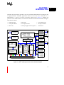
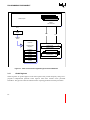
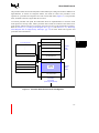
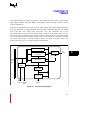
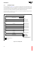
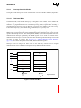
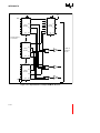
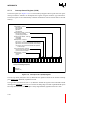
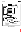
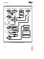
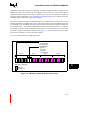
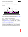
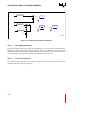
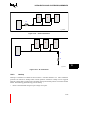
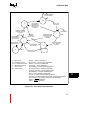
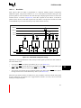
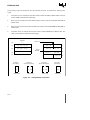
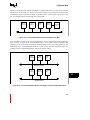
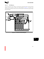
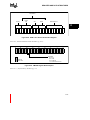
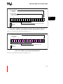
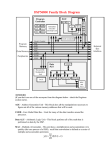
i960® Jx Microprocessor Functional Block Diagram............................................ 1-3
Data Types and Ranges ...................................................................................... 2-1
Data Placement in Registers ............................................................................... 2-6
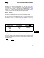
i960® Jx Processor Programming Environment Elements .................................. 3-2
Memory Address Space .................................................................................... 3-13
Arithmetic Controls (AC) Register...................................................................... 3-18
Process Controls (PC) Register......................................................................... 3-21
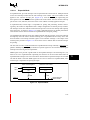
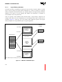
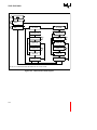
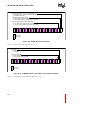
Internal Data RAM and Register Cache .............................................................. 4-2
Machine-Level Instruction Formats...................................................................... 5-3
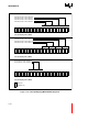
dcctl src1 and src/dst Formats ........................................................................... 6-41
Store Data Cache to Memory Output Format .................................................... 6-42
D-Cache Tag and Valid Bit Formats .................................................................. 6-43
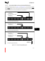
icctl src1 and src/dst Formats ............................................................................ 6-59
Store Instruction Cache to Memory Output Format ........................................... 6-61
I-Cache Set Data, Tag and Valid Bit Formats.................................................... 6-62
Src1 Operand Interpretation ............................................................................ 6-114
src/dst Interpretation for Breakpoint Resource Request .................................. 6-115
Procedure Stack Structure and Local Registers.................................................. 7-3
Frame Spill........................................................................................................... 7-9
Frame Fill ........................................................................................................... 7-10
System Procedure Table ................................................................................... 7-16
Previous Frame Pointer Register (PFP) (r0)...................................................... 7-20
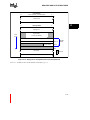
Fault-Handling Data Structures ........................................................................... 8-1
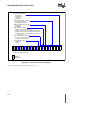
Fault Table and Fault Table Entries..................................................................... 8-5
Fault Record ........................................................................................................ 8-7
Storage of the Fault Record on the Stack............................................................ 8-8
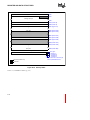
80960Jx Trace Controls (TC) Register ................................................................ 9-2
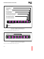
Breakpoint Control Register (BPCON)................................................................. 9-8
Data Address Breakpoint (DAB) Register Format ............................................. 9-10
Instruction Breakpoint (IPB) Register Format .................................................... 9-10
Timer Functional Diagram ................................................................................. 10-1
Timer Mode Register (TMR0, TMR1) ................................................................ 10-3
Timer Count Register (TCR0, TCR1)................................................................. 10-6
Timer Reload Register (TRR0, TRR1)............................................................... 10-7
Timer Unit State Diagram ................................................................................ 10-13
Interrupt Handling Data Structures .................................................................... 11-2
Interrupt Table ................................................................................................... 11-4
Storage of an Interrupt Record on the Interrupt Stack ....................................... 11-7
Dedicated Mode............................................................................................... 11-14
Figure 11-5.
Figure 11-6.
Figure 11-7.
Figure 11-8.
Figure 11-9.
Figure 11-10.
Figure 11-11.
Figure 11-12.
Figure 11-13.
Figure 12-1.
Figure 12-2.
Figure 12-3.
Figure 12-4.
Figure 12-5.
Figure 12-6.
Figure 12-7.
Figure 12-8.
Figure 12-9.
Figure 12-10.
Figure 12-11.
Figure 12-12.
Figure 12-13.
Figure 13-1.
Figure 13-2.
Figure 13-3.
Figure 13-4.
Figure 13-5.
Figure 13-6.
Figure 14.1.
Figure 14-2.
Figure 14-3.
Figure 14-4.
Figure 14-5.
Figure 14-6.
Figure 14-7.
Figure 14-8.
Figure 14-9.
Figure 14-10.
Figure 14-11.
Expanded Mode .............................................................................................. 11-15
Implementation of Expanded Mode Sources................................................... 11-16
Interrupt Sampling ........................................................................................... 11-20
Interrupt Control (ICON) Register.................................................................... 11-22
Interrupt Mapping (IMAP0-IMAP2) Registers .................................................. 11-24
Interrupt Pending (IPND) Register................................................................... 11-25
Interrupt Mask (IMSK) Registers ..................................................................... 11-26
Interrupt Controller........................................................................................... 11-30
Interrupt Service Flowchart.............................................................................. 11-34
Processor Initialization Flow .............................................................................. 12-2
Cold Reset Waveform ....................................................................................... 12-4
FAIL Sequence .................................................................................................. 12-8
Initial Memory Image (IMI) and Process Control Block (PRCB) ...................... 12-12
PMCON14_15 Register Bit Description in IBR ................................................ 12-15
Process Control Block Configuration Words.................................................... 12-17
Control Table ................................................................................................... 12-21
IEEE 1149.1 Device Identification Register..................................................... 12-22
VCC5 Current-Limiting Resistor........................................................................ 12-35
Reducing Characteristic Impedance................................................................ 12-36
Series Termination ......................................................................................... 12-39
AC Termination................................................................................................ 12-39
Avoid Closed-Loop Signal Paths ..................................................................... 12-41
PMCON and LMCON Example ......................................................................... 13-2
PMCON Register Bit Description....................................................................... 13-5
Bus Control Register (BCON)............................................................................ 13-6
Logical Memory Template Starting Address Registers (LMADR0-1) ................ 13-8
Logical Memory Template Mask Registers (LMMR0-1) .................................... 13-9
Default Logical Memory Configuration Register (DLMCON) ........................... 13-10
Bus States with Arbitration ................................................................................ 14-3
Data Width and Byte Encodings........................................................................ 14-7
Non-Burst Read and Write Transactions Without Wait States, 32-Bit Bus...... 14-10
32-Bit Wide Data Bus Bursts ........................................................................... 14-12
16-Bit Wide Data Bus Bursts ........................................................................... 14-12
8-Bit Wide Data Bus Bursts ............................................................................. 14-13
Unaligned Write Transaction ........................................................................... 14-14
Burst Read and Write Transactions w/o Wait States, 32-bit Bus..................... 14-15
Burst Read and Write Transactions w/o Wait States, 8-bit Bus....................... 14-16
Burst Write Transactions With 2,1,1,1 Wait States, 32-bit Bus........................ 14-18
Burst Read/Write Transactions with 1,0 Wait States - Extra Tr State
on Read, 16-Bit Bus ........................................................................................ 14-20
xviii
Figure 14-12. Burst Read/Write Transactions with 1,0 Wait States, Extra Tr State
on Read, 16-Bit Bus
14-21
Figure 14-13. Summary of Aligned and Unaligned Accesses (32-Bit Bus) ............................ 14-25
Figure 14-14. Summary of Aligned and Unaligned Accesses (32-Bit Bus) (Continued) ........ 14-26
Figure 14-15. Accesses Generated by Double Word Read Bus Request, Misaligned
One Byte From Quad Word Boundary, 32-Bit Bus, Little Endian
14-27
Figure 14-16. Multi-Word Access to Big-Endian Memory Space ........................................... 14-29
Figure 14-17. The LOCK Signal ............................................................................................. 14-31
Figure 14-18. Arbitration Timing Diagram for a Bus Master................................................... 14-33
Figure 14-19. Generalized 80960Jx System with 80960 Local Bus....................................... 14-35
Figure 14-20. Generalized 80960Jx System with 80960 Local Bus and Backplane Bus....... 14-35
Figure 14-21. 80960Jx System with 80960 Local Bus, PCI Local Bus and Local Bus
for High End Microprocessor
14-36
Figure 15-1.
Test Access Port Block Diagram ....................................................................... 15-3
Figure 15-2.
TAP Controller State Diagram ........................................................................... 15-4
Figure 15-3.
JTAG Example................................................................................................. 15-16
Figure 15-4.
Timing diagram illustrating the loading of Instruction Register ........................ 15-17
Figure 15-5.
Timing diagram illustrating the loading of Data Register ................................. 15-18
Figure C-1.
Instruction Formats ............................................................................................. C-1
Figure D-1.
AC (Arithmetic Controls) Register....................................................................... D-3
Figure D-2.
PC (Process Controls) Register.......................................................................... D-4
Figure D-3.
Procedure Stack Structure and Local Registers................................................. D-5
Figure D-4.
System Procedure Table .................................................................................... D-6
Figure D-5.
PFP (Previous Frame Pointer) Register (r0)....................................................... D-7
Figure D-6.
Fault Table and Fault Table Entries.................................................................... D-8
Figure D-7.
Fault Record ....................................................................................................... D-9
Figure D-8.
TC (Trace Controls) Register............................................................................ D-10
Figure D-9.
BPCON (Breakpoint Control) Register.............................................................. D-10
Figure D-10. DAB (Data Address Breakpoint) Register Format ............................................ D-11
Figure D-11. IPB (Instruction Breakpoint) Register Format ................................................... D-11
Figure D-12. TMR0-1 (Timer Mode Register) ........................................................................ D-12
Figure D-13. TCR0-1 (Timer Count Register)........................................................................ D-12
Figure D-14. TRR0-1 (Timer Reload Register) ...................................................................... D-13
Figure D-15. Interrupt Table .................................................................................................. D-14
Figure D-16. Storage of an Interrupt Record on the Interrupt Stack ...................................... D-15
Figure D-17. ICON (Interrupt Control) Register ..................................................................... D-16
Figure D-18. IMAP0-IMAP2 (Interrupt Mapping) Registers ................................................... D-17
Figure D-19. IMSK (Interrupt Mask) Registers....................................................................... D-18
Figure D-20. Interrupt Pending (IPND) Register .................................................................... D-19
Figure D-21. Initial Memory Image (IMI) and Process Control Block (PRCB) ....................... D-20
Figure D-22. Process Control Block Configuration Words..................................................... D-21
xix
Figure D-23.
Figure D-24.
Figure D-25.
Figure D-26.
Figure D-27.
Figure D-28.
Figure D-29.
Control Table ..................................................................................................... D-22
IEEE 1149.1 Device Identification Register....................................................... D-23
PMCON Register Bit Description....................................................................... D-23
BCON (Bus Control) Register............................................................................ D-24
DLMCON (Default Logical Memory Configuration) Register ............................. D-24
LMADR0:1 Logical Memory Template Starting Address Registers ................... D-25
LMMR0:1 (Logical Memory Mask Registers)..................................................... D-25
xx
TABLES
Table 1-1.
Table 2-1.
Table 2-2.
Table 2-3.
Table 3-1.
Table 3-2.
Table 3-3.
Table 3-4.
Table 3-5.
Table 3-6.
Table 3-7.
Table 3-8.
Table 3-9.
Table 3-10.
Table 5-1.
Table 5-2.
Table 5-3.
Table 6-1.
Table 6-2.
Table 6-3.
Table 6-4.
Table 6-5.
Table 6-6.
Table 6-7.
Table 6-8.
Table 6-9.
Table 6-10.
Table 6-11.
Table 6-12.
Table 6-13.
Table 6-15.
Table 6-16.
Table 6.17.
Table 6-18.
Table 6-19.
Table 6-20.
Table 7-1.
Table 7-2.
Table 8-1.
Register Terminology Conventions ................................................................... 1-10
Memory Contents for Little and Big Endian Example .......................................... 2-5
Byte Ordering for Little and Big Endian Accesses ............................................... 2-5
Memory Addressing Modes ................................................................................. 2-6
Registers and Literals Used as Instruction Operands ......................................... 3-3
Allowable Register Operands .............................................................................. 3-5
Access Types ...................................................................................................... 3-8
Supervisor Space Family Registers .................................................................... 3-9
User Space Family Registers and Tables ........................................................ 3-11
Data Structure Descriptions............................................................................... 3-12
Alignment of Data Structures in the Address Space ......................................... 3-15
Condition Codes for True or False Conditions .................................................. 3-19
Condition Codes for Equality and Inequality Conditions.................................... 3-19
Condition Codes for Carry Out and Overflow .................................................... 3-19
Instruction Encoding Formats .............................................................................. 5-2
80960Jx Instruction Set ....................................................................................... 5-4
Arithmetic Operations .......................................................................................... 5-7
Pseudo-Code Symbol Definitions ........................................................................ 6-4
Faults Applicable to All Instructions..................................................................... 6-4
Common Faulting Conditions .............................................................................. 6-5
Condition Code Mask Descriptions ..................................................................... 6-7
Condition Code Mask Descriptions ................................................................... 6-21
Condition Code Settings.................................................................................... 6-31
Condition Code Settings.................................................................................... 6-32
Condition Code Settings.................................................................................... 6-33
Condition Code Mask Descriptions ................................................................... 6-36
concmpo example: register ordering and CC .................................................... 6-39
dcctl Operand Fields.......................................................................................... 6-40
DCCTL Status Values and D-Cache Parameters.............................................. 6-42
Condition Code Mask Descriptions ................................................................... 6-52
icctl Operand Fields ........................................................................................... 6-58
ICCTL Status Values and Instruction Cache Parameters.................................. 6-60
Condition Code Mask Descriptions ................................................................... 6-97
sysctl Field Definitions ..................................................................................... 6-114
Cache Mode Configuration .............................................................................. 6-115
Condition Code Mask Descriptions ................................................................. 6-118
Encodings of Entry Type Field in System Procedure Table .............................. 7-17
Encoding of Return Status Field........................................................................ 7-21
i960® Jx Processor Fault Types and Subtypes ................................................... 8-3
xxi
Table 8-2.
Table 9-1.
Table 9-2.
Table 9-3.
Table 9-4.
Table 9-5.
Table 9-6.
Table 9-7.
Table 9-8.
Table 9-9.
Table 10-1.
Table 10-2.
Table 10-3.
Table 10-4.
Table 10-5.
Table 10-6.
Table 10-7.
Table 11-1.
Table 11-2.
Table 11-3.
Table 11-4.
Table 11-5.
Table 11-6.
Table 11-7.
Table 11-8.
Table 12-1.
Table 12-2.
Table 12-3.
Table 12-4.
Table 12-5.
Table 12-6.
Table 12-7.
Table 13-1.
Table 13-2.
Table 14-1.
Table 14-2.
Table 14-3.
Table 14-4.
Table 14-5.
Table 14-6.
xxii
Fault Control Bits and Masks............................................................................. 8-16
src/dst Encoding .................................................................................................. 9-7
Configuring the Data Address Breakpoint (DAB) Registers................................ 9-8
Programming the Data Address Breakpoint (DAB) Modes.................................. 9-8
Instruction Breakpoint Modes ............................................................................ 9-11
Tracing on Explicit Call ...................................................................................... 9-13
Tracing on Implicit Call ...................................................................................... 9-14
Tracing on Return from Explicit Call .................................................................. 9-15
Tracing on Return from Fault ............................................................................. 9-15
Tracing on Return from Interrupt ....................................................................... 9-16
Timer Performance Ranges............................................................................... 10-2
Timer Registers ................................................................................................. 10-2
Timer Input Clock (TCLOCK) Frequency Selection ........................................... 10-6
Timer Mode Register Control Bit Summary ....................................................... 10-8
Timer Responses to Register Bit Settings ......................................................... 10-9
Timer Powerup Mode Settings ........................................................................ 10-11
Uncommon TMRx Control Bit Settings ............................................................ 10-12
Interrupt Control Registers Memory-Mapped Addresses................................. 11-21
Location of Cached Vectors in Internal RAM ................................................... 11-36
Base Interrupt Latency..................................................................................... 11-37
Worst-Case Interrupt Latency Controlled by divo to Destination r15 ............... 11-38
Worst-Case Interrupt Latency Controlled by divo to Destination r3 ................. 11-39
Worst-Case Interrupt Latency Controlled by calls............................................ 11-39
Worst-Case Interrupt Latency When Delivering a Software Interrupt .............. 11-40
Worst-Case Interrupt Latency Controlled by flushreg of One Stack Frame..... 11-41
Reset States ...................................................................................................... 12-5
Register Values After Reset .............................................................................. 12-5
Fail Codes For BIST (bit 7 = 1) .......................................................................... 12-9
Remaining Fail Codes (bit 7 = 0) ....................................................................... 12-9
Initialization Boot Record ................................................................................. 12-13
PRCB Configuration ........................................................................................ 12-16
Input Pins......................................................................................................... 12-37
PMCON Address Mapping ................................................................................ 13-4
DLMCON Values at Reset ............................................................................... 13-13
Summary of i960 Jx Processor Bus Signals ...................................................... 14-5
8-Bit Bus Width Byte Enable Encodings............................................................ 14-8
16-Bit Bus Width Byte Enable Encodings .......................................................... 14-8
32-Bit Bus Width Byte Enable Encodings .......................................................... 14-8
Natural Boundaries for Load and Store Accesses ........................................... 14-23
Summary of Byte Load and Store Accesses ................................................... 14-23
Table 14-7.
Table 14-8.
Table 14-9.
Table 14-10.
Table 14-11.
Table 15-1.
Table 15-2.
Table 15-3.
Table B-1.
Table B-2.
Table B-3.
Table B-4.
Table B-5.
Table B-6.
Table B-7.
Table B-8.
Table B-9.
Table B-10.
Table C-1.
Table C-2.
Table C-3.
Table C-4.
Table C-5.
Table C-6.
Table C-7.
Table D-1.
Summary of Short Word Load and Store Accesses ........................................ 14-23
Summary of n-Word Load and Store Accesses (n = 1, 2, 3, 4) ....................... 14-24
Byte Ordering on Bus Transfers, Word Data Type .......................................... 14-28
Byte Ordering on Bus Transfers, Short-Word Data Type ................................ 14-29
Byte Ordering on Bus Transfers, Byte Data Type ........................................... 14-29
TAP Controller Pin Definitions ........................................................................... 15-5
Boundary Scan Instruction Set .......................................................................... 15-8
Boundary Scan Register Bit Order .................................................................. 15-14
Miscellaneous Instruction Encoding Bits ............................................................. B-1
REG Format Instruction Encodings ..................................................................... B-2
COBR Format Instruction Encodings .................................................................. B-6
CTRL Format Instruction Encodings ................................................................... B-7
Cycle Counts for sysctl Operations ..................................................................... B-7
Cycle Counts for icctl Operations ........................................................................ B-8
Cycle Counts for dcctl Operations ....................................................................... B-8
Cycle Counts for intctl Operations ....................................................................... B-8
MEM Format Instruction Encodings .................................................................... B-9
Addressing Mode Performance ......................................................................... B-10
Instruction Field Descriptions .............................................................................. C-2
Encoding of src1 and src2 in REG Format .......................................................... C-3
Encoding of src/dst in REG Format ..................................................................... C-3
Encoding of src1 in COBR Format ...................................................................... C-3
Encoding of src2 in COBR Format ...................................................................... C-4
Addressing Modes for MEM Format Instructions................................................. C-5
Encoding of Scale Field ....................................................................................... C-6
Register and Data Structures .............................................................................. D-1
xxiii
1
INTRODUCTION
CHAPTER 1
INTRODUCTION
The i960® Jx microprocessor provides a new set of essential enhancements for an emerging class
of high-performance embedded applications. Based on the i960 core architecture, it is
implemented in a proven 0.6 micron, three-layer metal process. Figure 1-1 identifies the
processor’s most notable features, each of which is described in subsections that follow the figure.
These features include:
•
instruction cache
•
data cache
•
bus controller unit
•
on-chip data RAM
•
local register cache
•
interrupt controller
•
timer units
•
memory-mapped control registers •
CLKIN
TAP
5
Physical
Region
32-bit buses
Configuration
address
/ data
PLL, Clocks,
Power Mgmt
Instruction Cache
80960JT: 16 Kbyte
80960JF, JD: 4 Kbyte
80960JA: 2 Kbyte
Two-way Set Associative
Boundary Scan
Controller
Bus
Control Unit
Bus Request
Queues
Instruction Sequencer
Constants
21
Address/
Data Bus
32
Interrupt
Programmable Port
Interrupt Controller
9
SRC1
SRC2
DEST
effective
address
Memory
Interface
Unit
Memory Mapped
Register Interface
32-bit Addr
32-bit Data
1 Kbyte
Data RAM
Three Independent 32-Bit SRC1, SRC2, and DEST Buses
DEST
Execution
and
Address
Generation
Unit
SRC1
Multiply
Divide
Unit
SRC1
SRC2
DEST
Global / Local
Register File
SRC1 SRC2 DEST
Control
Two 32-Bit
Timers
Control
7-Set
Local Register Cache
128
external bus
Direct Mapped
Data Cache
JT: 4 Kbyte
JF, JD: 2 Kbyte
JA: 1 Kbyte
Figure 1-1. i960® Jx Microprocessor Functional Block Diagram
1-3
1
INTRODUCTION
1.1
PRODUCT FEATURES
The i960 Jx processor brings many enhancements to the i960 microprocessor family, including:
•
Improvements to the core architecture
•
Low power mode
•
New instructions
•
Improved cache design
•
Enhanced bus control unit
•
Improved interrupt performance
•
JTAG testability
1.1.1
Instruction Cache
The i960 JT processor features a 16 Kbyte two-way set-associative instruction cache. The i960 JF
and JD processors employ a 4-Kbyte, two-way set-associative instruction cache. i960 JA processors
feature a 2-Kbyte instruction cache. A mechanism is provided that allows software to lock critical
code within each “way” of the cache. The cache can be disabled and is managed by use of the icctl
and sysctl instructions, as described in section 4.4, “INSTRUCTION CACHE” (pg. 4-4).
1.1.2
Data Cache
The i960 JT processor features a 4 Kbyte direct-mapped data cache. The i960 JF and JD
processors feature a 2-Kbyte, direct-mapped data cache that is write-through and write-allocate.
i960 JA processors feature a 1-Kbyte direct-mapped data cache. These processors have a line size
of four words and implement a “natural” fill policy. Each line in the cache has a valid bit; to
reduce fetch latency on cache misses, each word within a line also has a valid bit. See section 4.5,
“DATA CACHE” (pg. 4-6) for details.
The data cache is managed through the dcctl instruction; see section 6.2.23, “dcctl” (pg. 6-40).
1.1.3
On-chip (Internal) Data RAM
The processor’s 1 Kbyte internal data RAM is accessible to software with an access time of
1 cycle per word. This RAM is mapped to the physical address range of 0 to 3FFH. The first
64 bytes are reserved for the caching of dedicated-mode interrupt vectors; this reduces interrupt
latency for these interrupts. In addition, write-protection for the first 64 bytes is provided to guard
against the effects of using null pointers in ‘C’ and to protect the cached interrupt vectors.
1-4
INTRODUCTION
The i960 processor compilers can take advantage of the internal data RAM; profiling compilers
can allocate the most frequently used variables into this RAM. See Section 4.1, INTERNAL
DATA RAM (pg. 4-1) for more detail.
1.1.4
Local Register Cache
The processor provides fast storage of local registers for call and return operations by using an
internal local register cache. This cache can store up to seven local register sets; additional register
sets must be saved in external memory.
The processor uses a 128-bit wide bus to store local register sets quickly to the register cache. To
reduce interrupt latency for high-priority interrupts, the number of sets that can be used by code
that is running at a lower priority or that is not interrupted can be restricted by programming the
register configuration word in the PRCB. This ensures that there are always sets available for
high-priority interrupt code without needing to save sets in external memory first. See Section 4.2,
LOCAL REGISTER CACHE (pg. 4-2) for more details.
1.1.5
Interrupt Controller
The interrupt controller unit (ICU) provides a flexible, low-latency means for requesting interrupts.
It handles the posting of interrupts requested by hardware and software sources. Acting independently from the core, the interrupt controller compares the priorities of posted interrupts with the
current process priority, off-loading this task from the core. The interrupt controller is compatible
with i960 CA/CF processors.
The interrupt controller provides the following features for handling hardware-requested interrupts:
•
Support of up to 240 external sources.
•
Eight external interrupt pins, one non-maskable interrupt (NMI) pin for detection of
hardware-requested interrupts and two internal timer sources.
•
Edge or level detection on external interrupt pins.
•
Debounce option on external interrupt pins.
The application program interfaces to the interrupt controller with six memory-mapped control
registers. The interrupt control register (ICON) and interrupt map control registers
(IMAP0-IMAP2) provide configuration information. The interrupt pending (IPND) register posts
hardware-requested interrupts. The interrupt mask (IMSK) register selectively masks
hardware-requested interrupts.
The interrupt inputs can be configured to be triggered on level-low or falling-edge signals.
Sampling of the input pins can be either debounced sampling or fast sampling.
1-5
1
INTRODUCTION
The i960 Jx processor has approximately 5 to 10 times faster interrupt servicing than the i960 Kx
processor. This is accomplished through a number of features:
•
a hardware priority resolver removes the need to access the external interrupt table to resolve
interrupts
•
caching of dedicated-mode interrupt vectors in the internal data RAM
•
reserving frames in the local register cache for high-priority interrupts
•
the ability to lock the code of interrupt service routines in the instruction-cache reduces the
fetch latency for starting up these routines
CHAPTER 11, INTERRUPTS discusses this in more detail.
1.1.6
Timer Support
The i960 Jx processor provides two identical 32-bit timers. Access to the timers is through
memory-mapped registers. The timers have a single-shot mode and auto-reload capabilities for
continuous operation. Each timer has an independent interrupt request to the i960 Jx processor
interrupt controller. See CHAPTER 10, TIMERS for a complete description.
1.1.7
Memory-Mapped Control Registers (MMR)
Control registers in the i960 Jx processor are memory-mapped to allow for visibility to application
software. This includes registers for memory configuration, internally cached PRCB data,
breakpoint registers, and interrupt control. These registers are mapped to the architecturally
reserved address space range of FF00 0000H to FFFF FFFFH. The processor ensures that accesses
to the MMRs generate no external bus cycles.
Section 3.3, MEMORY-MAPPED CONTROL REGISTERS (pg. 3-6) discusses this in more
detail.
1.1.8
External Bus
The 32-bit multiplexed external bus connects the i960 Jx processor to memory and I/O. This high
bandwidth bus provides burst transfer capability allowing up to four successive 32-bit data word
transfers at a maximum rate of one word every clock cycle. In addition to the bus signals, the i960
Jx processor provides signals to allow external bus masters. Lastly, the processor provides
variable bus-width support (8-, 16-, and 32-bit).
1-6
INTRODUCTION
1.1.9
Complete Fault Handling and Debug Capabilities
To aid in program development, the i960 Jx processor detects faults (exceptions). When a fault is
detected, the processors make an implicit call to a fault handling routine. Information collected for
each fault allows a program developer to quickly correct faulting code. The processors also allow
automatic recovery from most faults.
To support system debug, the i960 architecture provides a mechanism for monitoring processor
activities through a software tracing facility. This processor can be configured to detect as many as
seven different trace events, including breakpoints, branches, calls, supervisor calls, returns,
prereturns and the execution of each instruction (for single-stepping through a program). The
processors also provide four breakpoint registers that allow break decisions to be made based upon
instruction or data addresses.
1.2
ABOUT THIS MANUAL
This i960® Jx Microprocessor User’s Manual provides detailed programming and hardware
design information for the i960 Jx microprocessors. It is written for programmers and hardware
designers who understand the basic operating principles of microprocessors and their systems.
This manual does not provide electrical specifications such as DC and AC parametrics, operating
conditions and packaging specifications. Such information is found in the product’s data sheets:
•
80960JA/JF Embedded 32-bit Microprocessor Data Sheet (272504)
•
80960JD Embedded 32-bit Microprocessor Data Sheet (272596)
•
80L960JA/JF 3.3 V Embedded 32-bit Microprocessor Data Sheet (272744)
•
80960JA/JF 3.3 V Embedded 32-bit Microprocessor Data Sheet (273146)
•
80960JD 3.3 V Embedded 32-bit Microprocessor Data Sheet (272971)
•
80960JT 3.3 V Embedded 32-bit Microprocessor Data Sheet (273109)
Each document has a corresponding Specification Update document. These contain the latest technical
information about the product and documentation, and are available from Intel’s website. For information on
other i960 processor family products or the architecture in general, refer to Intel's Solutions960®
Development Tools Catalog (270791). It lists all current i960 microprocessor family-related documents,
support components, boards, software development tools, debug tools and more.
This manual is organized in three parts; each part comprises multiple chapters and/or appendices.
The following briefly describes each part:
•
Part I - Programming the i960 Jx Microprocessor (chapters 2-10) details the programming
environment for the i960 Jx devices. Described here are the processor's registers, instruction set, data
types, addressing modes, interrupt mechanism, external interrupt interface and fault mechanism.
1-7
1
INTRODUCTION
•
Part II - System Implementation (chapters 11-17) identifies requirements for designing a system
around the i960 Jx components, such as external bus interface and interrupt controller. Also
described are programming requirements for the bus controller and processor initialization.
•
Part III - Appendices includes quick references for hardware design and programming.
Appendices are also provided which describe the internal architecture, how to write
assembly-level code to exploit the parallelism of the processor and considerations for writing
software that is portable among all members of the i960 microprocessor family.
1.3
NOTATION AND TERMINOLOGY
This section defines terminology and textual conventions that are used throughout the manual.
1.3.1
Reserved and Preserved
Certain fields in registers and data structures are described as being either reserved or preserved:
•
A reserved field is one that may be used by other i960 architecture implementations. Correct
treatment of reserved fields ensures software compatibility with other i960 processors. The
processor uses these fields for temporary storage; as a result, the fields sometimes contain
unusual values.
•
A preserved field is one that the processor does not use. Software may use preserved fields for
any function.
Reserved fields in certain data structures should be cleared (set to zero) when the data structure is
created. Clear the reserved fields when creating the Interrupt Table, Fault Table and System
Procedure Table. Software should not modify or rely on these reserved field values after a data
structure is created. When the processor creates the Interrupt or Fault Record data structure on the
stack, software should not depend on the value of the reserved fields within these data structures.
Some bits or fields in data structures and registers are shown as requiring specific encoding. These
fields should be treated as if they were reserved fields. They should be set to the specified value
when the data structure is created or when the register is initialized and software should not
modify or rely on the value after that.
Reserved bits in the Arithmetic Controls (AC) register can be cleared after initialization to ensure
compatibility with other i960 processor implementations. Reserved bits in the Process Controls
(PC) register and Trace Controls (TC) register should not be initialized. When the AC, PC and TC
registers are modified using modac, modpc or modtc instructions, the reserved locations in these
registers must be masked.
1-8
INTRODUCTION
Certain areas of memory may be referred to as reserved memory in this reference manual.
Reserved — when referring to memory locations — implies that an implementation of the i960
architecture may use this memory for some special purpose. For example, memory-mapped
peripherals might be located in reserved memory areas on future implementations.
1.3.2
Specifying Bit and Signal Values
The terms set and clear in this manual refer to bit values in register and data structures. When a bit
is set, its value is 1; when the bit is clear, its value is 0. Likewise, setting a bit means giving it a
value of 1 and clearing a bit means giving it a value of 0.
The terms assert and deassert refer to the logically active or inactive value of a signal or bit,
respectively. A signal is specified as an active 0 signal by an overbar. For example, the input is
active low and is asserted by driving the signal to a logic 0 value.
1.3.3
Representing Numbers
All numbers in this manual can be assumed to be base 10 unless designated otherwise. In text,
binary numbers are sometimes designated with a subscript 2 (for example, 0012). When it is
obvious from the context that a number is a binary number, the “2” subscript may be omitted.
Hexadecimal numbers are designated in text with the suffix H (for example, FFFF FF5AH). In
pseudo-code action statements in the instruction reference section and occasionally in text,
hexadecimal numbers are represented by adding the C-language convention “0x” as a prefix. For
example “FF7AH” appears as “0xFF7A” in the pseudo-code.
1.3.4
Register Names
Memory-mapped registers and several of the global and local registers are referred to by their
generic register names, as well as descriptive names which describe their function. The global
register numbers are g0 through g15; local register numbers are r0 through r15. However, when
programming the registers in user-generated code, make sure to use the instruction operand. i960
microprocessor compilers recognize only the instruction operands listed in Table 1-1. Throughout
this manual, the registers’ descriptive names, numbers, operands and acronyms are used interchangeably, as dictated by context.
Groups of bits and single bits in registers and control words are called either bits, flags or fields.
These terms have a distinct meaning in this manual:
bit
Controls a processor function; programmed by the user.
flag
Indicates status. Generally set by the processor; certain flags are user programmable.
field
A grouping of bits (bit field) or flags (flag field).
1-9
1
INTRODUCTION
Table 1-1. Register Terminology Conventions
Register Descriptive Name
Global Registers
Frame Pointer
Local Registers
Previous Frame Pointer
Stack Pointer
Return Instruction Pointer
Register Number
Instruction Operand
g0 - g15
g15
r0 - r15
r0
r1
r2
g0 - g14
fp
r3 - r15
pfp
sp
rip
Acronym
FP
PFP
SP
RIP
Specific bits, flags and fields in registers and control words are usually referred to by a register
abbreviation (in upper case) followed by a bit, flag or field name (in lower case). These items are
separated with a period. A position number designates individual bits in a field. For example, the
return type (rt) field in the previous frame pointer (PFP) register is designated as “PFP.rt”. The
least significant bit of the return type field is then designated as “PFP.rt0”.
1.4
RELATED DOCUMENTS
The following documents are useful when designing with and programming the i960 microprocessor. Check the Intel website or contact your local sales representative for more information on
obtaining Intel documents, including Specification Updates.
•
80960JA/JF Embedded 32-bit Microprocessor Data Sheet (272504)
•
80960JD Embedded 32-bit Microprocessor Data Sheet (272596)
•
80L960JA/JF 3.3 V Embedded 32-bit Microprocessor Data Sheet (272744)
•
80960JA/JF 3.3 V Embedded 32-bit Microprocessor Data Sheet (273146)
•
80960JD 3.3 V Embedded 32-bit Microprocessor Data Sheet (272971)
•
80960JT 3.3 V Embedded 32-bit Microprocessor Data Sheet (273109)
•
Solutions960® Development Tools Catalog (270791)
1-10
2
DATA TYPES AND MEMORY
ADDRESSING MODES
CHAPTER 2
DATA TYPES AND MEMORY ADDRESSING MODES
2
2.1
DATA TYPES
The instruction set references or produces several data lengths and formats. The i960® Jx
processor supports the following data types:
•
Integer (signed 8, 16 and 32 bits)
•
Ordinal (unsigned integer 8, 16, 32 and 64 bits)
•
Long-Word (64 bits)
•
Triple-Word (96 bits)
•
Quad-Word (128 bits)
•
Bit Field
•
Bit
Figure 2-1 illustrates the class, data type and length of each type supported by i960 processors.
8
Bits
Bit Field
31
Length
0
16
Bits
LSB of
Bit Field
15
32
Bits
Byte
0
7
Short
0
Word
31
0
64
Bits
Long
0
63
96
Bits
Triple-Word
0
95
128
Bits
Quad-Word
0
127
Class
Numeric
(Integer)
Numeric
(Ordinal)
Data Type
Range
Byte Integer
Short Integer
Integer
8 Bits
16 Bits
32 Bits
-2 7 to 27 -1
-215 to 215 -1
-231 to 231 -1
Byte Ordinal
8 Bits
16 Bits
0 to 216 -1
Short Ordinal
Ordinal
Long Ordinal
Bit
Bit Field
Non-Numeric
Length
32 Bits
64 Bits
1 Bit
0 to 28 -1
0 to 232 -1
0 to 264 - 1
N/A
1-32 Bits
Long-Word
64 Bits
Triple-Word
96 Bits
Quad-Word
128 Bits
Figure 2-1. Data Types and Ranges
2-1
DATA TYPES AND MEMORY ADDRESSING MODES
2.1.1
Integers
Integers are signed whole numbers that are stored and operated on in two’s complement format by
the integer instructions. Most integer instructions operate on 32-bit integers. Byte and short integers
are referenced by the byte and short classes of the load, store and compare instructions only.
Integer load or store size (byte, short or word) determines how sign extension or data truncation is
performed when data is moved between registers and memory.
For instructions ldib (load integer byte) and ldis (load integer short), a byte or short word in
memory is considered a two’s complement value. The value is sign-extended and placed in the
32-bit register that is the destination for the load.
ldib
7AH is loaded into a
FAH is loaded into a
ldis
05A5H is loaded into
85A5H is loaded into
register as 0000 007AH
register as FFFF FFFAH
a register as 0000 05A5H
a register as FFFF 85A5H
Example 2-1. Sign Extensions on Load Byte and Load Short
For instructions stib (store integer byte) and stis (store integer short), a 32-bit two’s complement
number in a register is stored to memory as a byte or short word. When register data is too large to
be stored as a byte or short word, the value is truncated and the integer overflow condition is
signalled. When an overflow occurs, either an AC register flag is set or the ARITHMETIC.INTEGER_OVERFLOW fault is generated, depending on the Integer Overflow Mask bit
(AC.om) in the AC register. CHAPTER 8, FAULTS describes the integer overflow fault.
For instructions ld (load word) and st (store word), data is moved directly between memory and a
register with no sign extension or data truncation.
2.1.2
Ordinals
Ordinals or unsigned integer data types are stored and treated as positive binary values. Figure 2-1
shows the supported ordinal sizes.
The large number of instructions that perform logical, bit manipulation and unsigned arithmetic
operations reference 32-bit ordinal operands. When ordinals are used to represent Boolean values,
1 = TRUE and 0 = FALSE. Most extended arithmetic instructions reference the long ordinal data
type. Only load (ldob and ldos), store (stob and stos), and compare ordinal instructions reference
the byte and short ordinal data types.
2-2
DATA TYPES AND MEMORY ADDRESSING MODES
Sign and sign extension are not considered when ordinal loads and stores are performed; the values
may, however, be zero-extended or truncated. A short word or byte load to a register causes the
value loaded to be zero-extended to 32 bits. A short word or byte store to memory truncates an
ordinal value in a register to fit the size of the destination memory. No overflow condition is
signalled in this case.
2.1.3
Bits and Bit Fields
The processor provides several instructions that perform operations on individual bits or bit fields
within register operands. An individual bit is specified for a bit operation by giving its bit number
and register. Internal registers always follow little endian byte order; the least significant bit
corresponds to bit 0 and the most significant bit corresponds to bit 31.
A bit field is any contiguous group of bits (up to 32 bits long) in a 32-bit register. Bit fields do not
span register boundaries. A bit field is defined by giving its length in bits (1-32) and the bit number
of its lowest numbered bit (0-31).
Loading and storing bit and bit-field data is normally performed using the ordinal load (ldo) and
store (sto) instructions. When an ldi instruction loads a bit or bit field value into a 32-bit register,
the processor appends sign extension bits. A byte or short store can signal an integer overflow
condition.
2.1.4
Triple- and Quad-Words
Triple- and quad-words refer to consecutive words in memory or in registers. Triple- and
quad-word load, store and move instructions use these data types to accomplish block movements.
No data manipulation (sign extension, zero extension or truncation) is performed in these instructions.
Triple- and quad-word data types can be considered a superset of the other data types described.
The data in each word subset of a quad-word is likely to be the operand or result of an ordinal,
integer, bit or bit field instruction.
2.1.5
Register Data Alignment
Several of the processor’s instructions operate on multiple-word operands. For example, the
load-long instruction (ldl) loads two words from memory into two consecutive registers. The least
significant data word is loaded into the lower order register. The most significant data word is
loaded into the higher order register.
2-3
2
DATA TYPES AND MEMORY ADDRESSING MODES
In cases where an instruction specifies a register number (and multiple, consecutive registers are
implied), the register number must be even when two registers are accessed (e.g., g0, g2) and an
integral multiple of four when three or four registers are accessed (e.g., g0, g4). When a register
reference for a source value is not properly aligned, the registers that the processor writes to are
undefined.
The i960 Jx processor does not require data alignment in external memory; the processor hardware
handles unaligned memory accesses automatically. Optionally, user software can configure the
processor to generate a fault on unaligned memory accesses.
2.1.6
Literals
The architecture defines a set of 32 literals that can be used as operands in many instructions.
These literals are ordinal (unsigned) values that range from 0 to 31 (5 bits). When a literal is used
as an operand, the processor expands it to 32 bits by adding leading zeros. When the instruction
requires an operand larger than 32 bits, the processor zero-extends the value to the operand size.
When a literal is used in an instruction that requires integer operands, the processor treats the
literal as a positive integer value.
2.2
BIT AND BYTE ORDERING IN MEMORY
All occurrences of numeric and non-numeric data types, except bits and bit fields, must start on a
byte boundary. Any data item occupying multiple bytes is stored as big endian or little endian. The
following sections further describe byte ordering.
2.2.1
Bit Ordering
Bits within bytes are numbered such that when the byte is viewed as a value, bit 0 is the least
significant bit and bit 7 is the most significant bit. For numeric values spanning several bytes, bit
numbers higher than 7 indicate successively higher bit numbers in bytes with higher addresses.
Unless otherwise noted, bits in illustrations in this manual are ordered such that the
higher-numbered bits are to the left.
2.2.2
Byte Ordering
The i960 Jx processor can be programmed to use little or big endian byte ordering for memory
accesses. Byte ordering refers to how data items larger than one byte are assembled:
•
For little endian byte order, the byte with the lowest address in a multi-byte data item has the
least significance.
•
For big endian byte order, the byte with the lowest address in a multi-byte data item has the
most significance.
2-4
DATA TYPES AND MEMORY ADDRESSING MODES
For example, Table 2-1 shows eight bytes of data in memory. Table 2-2 shows the differences
between little and big endian accesses for byte, short, word and long-word data. Figure 2-2 shows
the resultant data placement in registers.
Once data is read into registers, byte order is no longer relevant. The lowest significant bit is
always bit 0. The most significant bit is always bit 31 for words, bit 15 for short words, and bit 7
for bytes.
Byte ordering affects the way the i960 Jx processor handles bus accesses. See section 13.6.2,
“Selecting the Byte Order” (pg. 13-12) for more information.
Table 2-1. Memory Contents for Little and Big Endian Example
ADDRESS
DATA
1000H
12H
1001H
34H
1002H
56H
1003H
78H
1004H
9AH
1005H
BCH
1006H
DEH
1007H
F0H
Table 2-2. Byte Ordering for Little and Big Endian Accesses
Access
Example
Register Contents
(Little Endian)
Register Contents
(Big Endian)
Byte at 1000H
ldob 0x1000, r3
12H
12H
Short at 1002H
ldos 0x1002, r3
7856H
5678H
Word at 1000H
ld
0x1000, r3
78563412H
12345678H
Long-Word at 1000H
78563412H (r4)
12345678H (r4)
ldl
0x1000, r4
F0DEBC9AH (r5)
9ABCDEF0H (r5)
2-5
2
DATA TYPES AND MEMORY ADDRESSING MODES
31
Byte
24 23
XX
31
24 23
XX
Short
31
87
XX
16 15
XX
24 23
DD3
Word
16 15
XX
87
DD1
16 15
DD2
0
DD0
0
DD0
87
DD1
0
DD0
NOTES:
D’s are data transferred to/from memory
X’s are zeros for ordinal data
X’s are sign bit extensions for integer data
Figure 2-2. Data Placement in Registers
2.3
MEMORY ADDRESSING MODES
The processor provides nine modes for addressing operands in memory. Each addressing mode is used
to reference a byte location in the processor’s address space. Table 2-3 shows the memory addressing
modes and a brief description of each mode’s address elements and assembly code syntax.
Table 2-3. Memory Addressing Modes
Mode
Description
Assembler Syntax
Inst.
Type
offset offset (smaller than 4096)
exp
MEMA
displacement displacement (larger than 4095)
exp
MEMB
(reg)
MEMB
with offset abase + offset
exp (reg)
MEMA
with displacement abase + displacement
exp (reg)
MEMB
(reg) [reg*scale]
MEMB
abase + (index*scale) +
displacement
exp (reg)
[reg*scale]
MEMB
Index with displacement
(index*scale) + displacement
exp [reg*scale]
MEMB
instruction pointer (IP) with
displacement
IP + displacement + 8
exp (IP)
MEMB
Absolute
Register Indirect
abase
with index abase + (index*scale)
with index and displacement
NOTE: reg is register, exp is an expression or symbolic label, and IP is the Instruction Pointer.
2-6
DATA TYPES AND MEMORY ADDRESSING MODES
See Table B-9 in APPENDIX B for more on addressing modes. For purposes of this memory
addressing modes description, MEMA format instructions require one word of memory and
MEMB usually require two words and therefore consume twice the bus bandwidth to read.
Otherwise, both formats perform the same functions.
2.3.1
Absolute
Absolute addressing modes allow a memory location to be referenced directly as an offset from
address 0H. At the instruction encoding level, two absolute addressing modes are provided:
absolute offset and absolute displacement, depending on offset size.
•
For the absolute offset addressing mode, the offset is an ordinal number ranging from 0 to 4095.
The absolute offset addressing mode is encoded in the MEMA machine instruction format.
•
For the absolute displacement addressing mode, the offset value ranges from 0 to 232-1. The
absolute displacement addressing mode is encoded in the MEMB format.
Addressing modes and encoding instruction formats are described in CHAPTER 6,
INSTRUCTION SET REFERENCE.
At the assembly language level, the two absolute addressing modes use the same syntax. Typically,
development tools allow absolute addresses to be specified through arithmetic expressions
(e.g., x + 44) or symbolic labels. After evaluating an address specified with the absolute addressing
mode, the assembler converts the address into an offset or displacement and selects the appropriate
instruction encoding format and addressing mode.
2.3.2
Register Indirect
Register indirect addressing modes use a register’s 32-bit value as a base for address calculation.
The register value is referred to as the address base (designated “abase” in Table 2-3). Depending
on the addressing mode, an optional scaled index and offset can be added to this address base.
Register indirect addressing modes are useful for addressing elements of an array or record
structure. When addressing array elements, the abase value provides the address of the first array
element. An offset (or displacement) selects a particular array element.
In register-indirect-with-index addressing mode, the index is specified using a value contained in a
register. This index value is multiplied by a scale factor. Allowable factors are 1, 2, 4, 8 and 16. The
register-indirect-with-index addressing mode is encoded in the MEMB format.
The two versions of register-indirect-with-offset addressing mode at the instruction encoding level
are register-indirect-with-offset and register-indirect-with-displacement. As with absolute
addressing modes, the mode selected depends on the size of the offset from the base address.
2-7
2
DATA TYPES AND MEMORY ADDRESSING MODES
At the assembly language level, the assembler allows the offset to be specified with an expression
or symbolic label, then evaluates the address to determine whether to use register-indirect-withoffset (MEMA format) or register-indirect-with-displacement (MEMB format) addressing mode.
Register-indirect-with-index-and-displacement addressing mode adds both a scaled index and a
displacement to the address base. There is only one version of this addressing mode at the
instruction encoding level, and it is encoded in the MEMB instruction format.
2.3.3
Index with Displacement
A scaled index can also be used with a displacement alone. The index is contained in a register and
multiplied by a scaling constant before displacement is added. This mode uses MEMB format.
2.3.4
IP with Displacement
This addressing mode is used with load and store instructions to make them instruction pointer
(IP) relative. IP-with-displacement addressing mode references the next instruction’s address plus
the displacement. This mode uses MEMB format.
2.3.5
Addressing Mode Examples
The following examples show how i960 processor addressing modes are encoded in assembly
language. Example 2-2 shows addressing mode mnemonics. Example 2-3 illustrates the
usefulness of scaled index and scaled index plus displacement addressing modes. In this example,
a procedure named array_op uses these addressing modes to fill two contiguous memory blocks
separated by a constant offset. A pointer to the top of the block is passed to the procedure in g0, the
block size is passed in g1 and the fill data in g2.
For more details on encoding formats, refer to APPENDIX C, MACHINE-LEVEL
INSTRUCTION FORMATS.
2-8
DATA TYPES AND MEMORY ADDRESSING MODES
st
g4,xyz
ldob
(r3),r4
stl
g6,xyz(g5)
ldq
(r8)[r9*4],r4
st
g3,xyz(g4)[g5*2]
ldis
xyz[r12*2],r13
st
r4,xyz(ip)
#
#
#
#
#
#
#
#
#
#
#
#
#
#
#
#
#
#
#
Absolute; word from g4 stored at memory
location designated with label xyz.
Register indirect; ordinal byte from
memory location given in r3 loaded
into register r4 and zero extended.
Register indirect with displacement;
double word from g6,g7 stored at memory
location xyz + g5.
Register indirect with index; quad-word
beginning at memory location r8 + (r9
scaled by 4) loaded into r4 through r7.
Register indirect with index and
displacement; word in g3 stored to mem
location g4 + xyz + (g5 scaled by 2).
Index with displacement; load short
integer at memory location xyz + r12
into r13 and sign extended.
ip with displacement; store word in r4
at memory location IP + xyz + 8.
Example 2-2. Addressing Mode Mnemonics
array_op:
mov
subi
b
.I34:
st
st
subi
.I33:
cmpible
ret
g0,r4
1,g1,r3
.I33
# Pointer to array is copied to r4.
# Calculate index for the last array
# element to be filled
g2,(r4)[r3*4]
# Fill element at index
g2,0x30(r4)[r3*4] # Fill element at index+constant offset
1,r3,r3
# Decrement index
0,r3,.I34
# Store next array elements if
# index is not 0
Example 2-3. Scaled Index and Scaled Index Plus Displacement Addressing Modes
2-9
2
3
PROGRAMMING
ENVIRONMENT
CHAPTER 3
PROGRAMMING ENVIRONMENT
This chapter describes the i960® Jx processor’s programming environment including global and
local registers, control registers, literals, processor-state registers and address space.
3.1
OVERVIEW
The i960 architecture defines a programming environment for program execution, data storage and data
manipulation. Figure 3-1 shows the programming environment elements that include the following:
•
4 Gbyte (232 byte) flat address space
•
register cache
•
instruction cache
•
set of literals
•
data cache
•
control registers
•
global and local general-purpose registers
•
set of processor state registers
The processor includes several architecturally-defined data structures located in memory as part of
the programming environment. These data structures handle procedure calls, interrupts and faults
and provide configuration information at initialization. These data structures are:
•
interrupt stack
•
control table
•
system procedure table
•
local stack
•
fault table
•
process control block
•
supervisor stack
•
interrupt table
•
initialization boot record
3.2
REGISTERS AND LITERALS AS INSTRUCTION OPERANDS
With the exception of a few special instructions, the i960 Jx processor uses load and store instructions to access memory. All operations take place at the register level. The processor uses 16 global
registers, 16 local registers and 32 literals (constants 0-31) as instruction operands.
The global register numbers are g0 through g15; local register numbers are r0 through r15. Several
of these registers are used for dedicated functions. For example, register r0 is the previous frame
pointer, often referred to as pfp. The i960 processor compilers and assemblers recognize only the
instruction operands listed in Table 3-1. Throughout this manual, the registers’ descriptive names,
numbers, operands and acronyms are used interchangeably, as dictated by context.
3-1
3
PROGRAMMING ENVIRONMENT
FFFF FFFFH
0000 0000H
Address Space
Architecturally
Defined
Data Structures
Fetch
Instruction
Cache
Load
Store
Instruction
Stream
Instruction
Execution
Processor State
Registers
Instruction
Pointer
Arithmetic
Controls
g0
g15
Sixteen 32-Bit
Global Registers
Register Cache r15
Sixteen 32-Bit
Local Registers
r0
r15
Process
Controls
Trace
Controls
Figure 3-1. i960® Jx Processor Programming Environment Elements
3.2.1
Global Registers
Global registers are general-purpose 32-bit data registers that provide temporary storage for a
program’s computational operands. These registers retain their contents across procedure
boundaries. They provide a fast and efficient means of passing parameters between procedures.
3-2
PROGRAMMING ENVIRONMENT
Table 3-1. Registers and Literals Used as Instruction Operands
Instruction Operand
Register Name (number)
Function
Acronym
g0 - g14
global (g0-g14)
general purpose
fp
global (g15)
frame pointer
FP
pfp
local (r0)
previous frame pointer
PFP
sp
local (r1)
stack pointer
SP
rip
local (r2)
return instruction pointer
RIP
r3 - r15
local (r3-r15)
general purpose
0-31
3
literals
The i960 architecture supplies 16 global registers, designated g0 through g15. Register g15 is
reserved for the current Frame Pointer (FP), which contains the address of the first byte in the
current (topmost) stack frame in memory. See CHAPTER 7, PROCEDURE CALLS for a
description of the FP and procedure stack.
After the processor is reset, register g0 contains device identification and stepping information
(DeviceID). Refer to Section 1.4, ”Related Documents” (pg. 1-10). Further information on Device
IDs can be found in these documents. The information is retained in g0 until it is written over by
the user program. The device identification and stepping information is also stored in the
memory-mapped DEVICEID register located at FF00 8710H.
3.2.2
Local Registers
The i960 architecture provides a separate set of 32-bit local data registers (r0 through r15) for each
active procedure. These registers provide storage for variables that are local to a procedure. Each
time a procedure is called, the processor allocates a new set of local registers and saves the calling
procedure’s local registers. When the application returns from the procedure, the local registers are
released for the next procedure call. The processor performs local register management; a program
need not explicitly save and restore these registers.
Local registers r3 through r15 are general purpose registers; r0 through r2 are reserved for special
functions; r0 contains the Previous Frame Pointer (PFP); r1 contains the Stack Pointer (SP); r2 contains
the Return Instruction Pointer (RIP). These are discussed in CHAPTER 7, PROCEDURE CALLS.
The processor does not always clear or initialize the set of local registers assigned to a new
procedure. Also, the processor does not initialize the local register save area in the newly created
stack frame for the procedure. User software should not rely on the initial values of local registers.
3-3
PROGRAMMING ENVIRONMENT
3.2.3
Register Scoreboarding
Register scoreboarding maintains register coherency by preventing parallel execution units from
accessing registers for which there is an outstanding operation. When an instruction that targets a
destination register or group of registers executes, the processor sets a register-scoreboard bit to
indicate that this register or group of registers is being used in an operation. When the instructions
that follow do not require data from registers already in use, the processor can execute those
instructions before the prior instruction completes execution.
Software can use this feature to execute one or more single-cycle instructions concurrently with a
multi-cycle instruction (e.g., multiply or divide). Example 3-1 shows a case where register scoreboarding prevents a subsequent instruction from executing. It also illustrates overlapping instructions that do not have register dependencies.
Example 3-1. Register Scoreboarding
muli r4,r5,r6
addi r6,r7,r8
.
.
.
muli r4,r5,r10
and r6,r7,r8
3.2.4
# r6 is scoreboarded
# addi must wait for the previous multiply
# to complete
# r10 is scoreboarded
# and instruction is executed concurrently with multiply
Literals
The architecture defines a set of 32 literals that can be used as operands in many instructions.
These literals are ordinal (unsigned) values that range from 0 to 31 (5 bits). When a literal is used
as an operand, the processor expands it to 32 bits by adding leading zeros. When the instruction
requires an operand larger than 32 bits, the processor zero-extends the value to the operand size.
When a literal is used in an instruction that requires integer operands, the processor treats the
literal as a positive integer value.
3.2.5
Register and Literal Addressing and Alignment
Several instructions operate on multiple-word operands. For example, the load long instruction
(ldl) loads two words from memory into two consecutive registers. The register for the less
significant word is specified in the instruction. The more significant word is automatically loaded
into the next higher-numbered register.
3-4
PROGRAMMING ENVIRONMENT
In cases where an instruction specifies a register number and multiple consecutive registers are
implied, the register number must be even when two registers are accessed (e.g., g0, g2) and an
integral multiple of 4, when 3 or 4 registers are accessed (e.g., g0, g4). When a register reference
for a source value is not properly aligned, the source value is undefined and an
OPERATION.INVALID_OPERAND fault is generated. When a register reference for a
destination value is not properly aligned, the registers to which the processor writes and the values
written are undefined. The processor then generates an OPERATION.INVALID_OPERAND fault.
The assembly language code in Example 3-2 shows an example of correct and incorrect register
alignment.
Example 3-2. Register Alignment
movl g3,g8
.
.
.
movl g4,g8
# Incorrect alignment - resulting value
# in registers g8 and g9 is
# unpredictable (non-aligned source)
# Correct alignment
Global registers, local registers and literals are used directly as instruction operands. Table 3-2 lists
instruction operands for each machine-level instruction format and the positions that can be filled
by each register or literal.
Table 3-2. Allowable Register Operands
Operand (1)
Instruction
Encoding
Local Register
Global
Register
REG
src1
src2
src/dst (as src)
src/dst (as dst)
src/dst (as both)
X
X
X
X
X
X
X
X
X
X
MEM
src/dst
abase
index
X
X
X
X
X
X
COBR
src1
src2
dst
X
X
X (2)
X
X
X (2)
Operand Field
Literal
X
X
X
NOTES:
1. 1.“X” denotes the register can be used as an operand in a particular instruction field.
2. The COBR destination operands apply only to TEST instructions.
3-5
3
PROGRAMMING ENVIRONMENT
3.3
MEMORY-MAPPED CONTROL REGISTERS
The i960 Jx processor gives software the interface to easily read and modify internal control
registers. Each of these registers is accessed as a 32-bit memory-mapped register (MMR) with a
unique memory address. The processor ensures that accesses to MMRs do not generate external
bus cycles.
3.3.1
Memory-Mapped Registers (MMR)
Portions of the i960 Jx processor address space (addresses FF00 0000H through FFFF FFFFH) are
reserved for memory-mapped registers (see section 12.3, “Architecturally Reserved Memory
Space” (pg. 12-9). These memory-mapped registers (MMRs) are accessed through word-operand
memory instructions (ld and st instructions) and some register class instructions (atmod, atadd
and sysctl). Accesses to the MMRs do not generate external bus cycles. The latency in accessing
each of these registers is one cycle for ld and st and multiple cycles for others.
Each register has an associated access mode (user and supervisor modes) and access type (read
and write accesses). Table 3-4 and Table 3-5 show all the memory-mapped registers and the
application modes of access.
The registers are partitioned into user and supervisor spaces based on their addresses. Addresses
FF00 0000H through FF00 7FFFH are allocated to user space memory-mapped registers;
Addresses FF00 8000H to FFFF FFFFH are allocated to supervisor space registers.
3.3.1.1
Restrictions on Instructions that Access Memory-Mapped Registers
The majority of memory-mapped registers can be accessed by both load (ld) and store (st) instructions. However some registers have restrictions on the types of access they allow. To ensure correct
operation, the access type restrictions for each register should be followed. The access type
columns of Table 3-4 and Table 3-5 indicate the allowed access types for each register.
Unless otherwise indicated by its access type, the modification of a memory-mapped register by a
st instruction takes effect completely before the next instruction starts execution.
Some operations require an atomic-read-modify-write sequence to a register, most notably IPND
and IMSK. The atmod and atadd instructions provide a special mechanism to quickly modify the
IPND and IMSK registers in an atomic manner on the i960 Jx processor. Do not use these
instruction on any other memory-mapped registers.
The sysctl instruction can also modify the contents of a memory-mapped register atomically; in
addition, sysctl is the only method to read the breakpoint registers on the i960 Jx processor; the
breakpoints cannot be read using a ld instruction.
3-6
PROGRAMMING ENVIRONMENT
At initialization, the control table automatically loads into the on-chip control registers. This action
simplifies the user’s start-up code by providing a transparent setup of the processor’s peripherals.
See CHAPTER 12, INITIALIZATION AND SYSTEM REQUIREMENTS.
3.3.1.2
Access Faults
Memory-mapped registers are meant to be accessed only as aligned, word-size registers with
adherence to the appropriate access mode. Accessing these registers in any other way results in
faults or undefined operation. An access is performed using the following fault model:
1.
The access must be a word-sized, word-aligned access; otherwise, the processor generates an
OPERATION.UNIMPLEMENTED fault.
2.
When the access is a store in user mode to an implemented supervisor location, a
TYPE.MISMATCH fault occurs. It is unpredictable whether a store to an unimplemented
supervisor location causes a fault.
3.
When the access is neither of the above, the access is attempted. Note that an MMR may
generate faults based on conditions specific to that MMR. (Example: trying to write the
timer registers in user mode when they have been allocated to supervisor mode only.)
4.
When a store access to an MMR faults, the processor ensures that the store does not take effect.
5.
A load access of a reserved location returns an unpredictable value.
6.
Avoid any store accesses to reserved locations. Such a store can result in undefined operation
of the processor when the location is in supervisor space.
Instruction fetches from the memory-mapped register space are not allowed and result in an
OPERATION.UNIMPLEMENTED fault.
3-7
3
PROGRAMMING ENVIRONMENT
Table 3-3. Access Types
Access Type
Description
R
Read
Read (ld instruction) accesses are allowed.
RO
Read
Only
Only Read (ld instruction) accesses are allowed. Write (st
instruction) accesses are ignored.
W
Write
Write (st instruction) accesses allowed.
R/W
Read/Write ld, st, and sysctl instructions are allowed access.
WwG
Write
when
Granted
Writing or Modifying (through a st or sysctl instruction) the register
is only allowed when modification-rights to the register have been
granted. An OPERATION.UNIMPLEMENTED fault occurs when an
attempt is made to write the register before rights are granted. See
section 9.2.7.2, “Hardware Breakpoints” (pg. 9-5) for details about
getting modification rights to breakpoint registers.
Sysctl-RwG
sysctl
Read
when
Granted
The value of the register can only be read by executing a sysctl
instruction issued with the modify memory-mapped register
message type. Modification rights to the register must be granted
first or an OPERATION.UNIMPLEMENTED fault occurs when the
sysctl is executed. A ld instruction to the register returns unpredictable results.
atmod
update
Register can be updated quickly through the atmod instruction. The
atmod ensures correct operation by performing the update of the
register in an atomic manner which provides synchronization with
previous and subsequent operations. This is a faster update
mechanism than sysctl and is optimized for a few special registers.
AtMod
3-8
PROGRAMMING ENVIRONMENT
Table 3-4. Supervisor Space Family Registers (Sheet 1 of 2)
Memory-Mapped
Address
Access Type
FF00 8000H to
FF00 80FFH
—
(DLMCON) Default Logical Memory Configuration
Register
FF00 8100H
R/W
Reserved
FF00 8104H
—
Register Name
Reserved
3
(LMADR0) Logical Memory Address Register 0
FF00 8108H
R/W
(LMMR0) Logical Memory Mask Register 0
FF00 810CH
R/W
(LMADR1) Logical Memory Address Register 1
FF00 8110H
R/W
(LMMR1) Logical Memory Mask Register 1
FF00 8114H
R/W
FF00 8118H to
FF00 83FFH
—
(IPB0) Instruction Address Breakpoint Register 0
FF00 8400H
Sysctl- RwG/WwG
(IPB1) Instruction Address Breakpoint Register 1
FF00 8404H
Sysctl- RwG/WwG
FF00 8408H to
FF00 841FH
—
FF00 8420H
R/W, WwG
Reserved
Reserved
(DAB0) Data Address Breakpoint Register 0
(DAB1) Data Address Breakpoint Register 1
FF00 8424H
R/W, WwG
FF00 8428H to
FF00 843FH
—
FF00 8440H
R/W, WwG
FF00 8444H to
FF00 84FFH
—
(IPND) Interrupt Pending Register
FF00 8500H
AtMod
(IMSK) Interrupt Mask Register
FF00 8504H
AtMod
FF00 8508H to
FF00 850FH
—
FF00 8510H
R/W
FF00 8514H to
FF00 851FH
—
(IMAP0) Interrupt Map Register 0
FF00 8520H
R/W
(IMAP1) Interrupt Map Register 1
FF00 8524H
R/W
(IMAP2) Interrupt Map Register 2
FF00 8528H
R/W
FF00 852CH to
FF00 85FFH
—
Reserved
(BPCON) Breakpoint Control Register
Reserved
Reserved
(ICON) Interrupt Control Word
Reserved
Reserved
3-9
PROGRAMMING ENVIRONMENT
Table 3-4. Supervisor Space Family Registers (Sheet 2 of 2)
Memory-Mapped
Address
Access Type
(PMCON0_1) Physical Memory Control Register 0
FF00 8600H
R/W
Register Name
Reserved
FF00 8604H
—
(PMCON2_3) Physical Memory Control Register 1
FF00 8608H
R/W
Reserved
FF00 860CH
—
(PMCON4_5) Physical Memory Control Register 2
FF00 8610H
R/W
Reserved
FF00 8614H
—
(PMCON6_7) Physical Memory Control Register 3
FF00 8618H
R/W
Reserved
FF00 861CH
—
(PMCON8_9) Physical Memory Control Register 4
FF00 8620H
R/W
Reserved
FF00 8624H
—
(PMCON10_11) Physical Memory Control Register 5
FF00 8628H
R/W
Reserved
FF00 862CH
—
(PMCON12_13) Physical Memory Control Register 6
FF00 8630H
R/W
Reserved
FF00 8634H
—
(PMCON14_15) Physical Memory Control Register 7
FF00 8638H
R/W
FF00 863CH to
FF00 86F8H
—
(BCON) Bus Configuration Control Register
FF00 86FCH
R/W
(PRCB) Processor Control Block Pointer
FF00 8700H
RO
(ISP) Interrupt Stack Pointer
FF00 8704H
R/W
(SSP) Supervisor Stack Pointer
FF00 8708H
R/W
Reserved
FF00 870CH
—
(DEVICEID) i960 Jx processor Device ID
FF00 8710H
RO
FF00 8714H to
FFFF FFFFH
—
Reserved
Reserved
3-10
PROGRAMMING ENVIRONMENT
Table 3-5. User Space Family Registers and Tables
Register Name
Memory-Mapped
Address
Access Type
FF00 0000H to
FF00 02FFH
—
FF00 0300H
R/W
Timers
Reserved
(TRR0) Timer Reload Register 0
(TCR0) Timer Count Register 0
FF00 0304H
R/W
(TMR0) Timer Mode Register 0
FF00 0308H
R/W
Reserved
FF00 030CH
—
(TRR1) Timer Reload Register 1
FF00 0310H
R/W
(TCR1) Timer Count Register 1
FF00 0314H
R/W
(TMR1) Timer Mode Register 1
FF00 0318H
R/W
FF00 031CH to
FF00 7FFFH
—
Reserved
3.4
3
ARCHITECTURALLY DEFINED DATA STRUCTURES
The architecture defines a set of data structures including stacks, interfaces to system procedures,
interrupt handling procedures and fault handling procedures. Table 3-6 defines the data structures
and references other sections of this manual where detailed information can be found.
The i960 Jx processor defines two initialization data structures: the Initialization Boot Record
(IBR) and the Process Control Block (PRCB). These structures provide initialization data and
pointers to other data structures in memory. When the processor is initialized, these pointers are
read from the initialization data structures and cached for internal use.
Pointers to the system procedure table, interrupt table, interrupt stack, fault table and control table
are specified in the processor control block. Supervisor stack location is specified in the system
procedure table. User stack location is specified in the user’s startup code. Of these structures, only
the system procedure table, fault table, control table and initialization data structures may be in
ROM; the interrupt table and stacks must be in RAM. The interrupt table must be located in RAM
to allow posting of software interrupts.
3-11
PROGRAMMING ENVIRONMENT
Table 3-6. Data Structure Descriptions
Structure (see also)
Description
User and Supervisor Stacks
section 7.6, “USER AND
SUPERVISOR STACKS”
(pg. 7-19)
The processor uses these stacks when executing application
code.
Interrupt Stack
section 11.5, “INTERRUPT
STACK AND INTERRUPT
RECORD” (pg. 11-7)
A separate interrupt stack is provided to ensure that interrupt
handling does not interfere with application programs.
System Procedure Table
Contains pointers to system procedures. Application code uses
the system call instruction (calls) to access system procedures
through this table. A system supervisor call switches execution
mode from user mode to supervisor mode. When the
processor switches modes, it also switches to the supervisor
stack.
section 3.8, “USER-SUPERVISOR PROTECTION MODEL”
(pg. 3-23)
section 7.5, “SYSTEM CALLS”
(pg. 7-15)
Interrupt Table
section 11.4, “INTERRUPT
TABLE” (pg. 11-4)
Fault Table
section 8.3, “FAULT TABLE”
(pg. 8-4)
Control Table
section 12.3.3, “Control Table”
(pg. 12-20)
3-12
The interrupt table contains vectors (pointers) to interrupt
handling procedures. When an interrupt is serviced, a
particular interrupt table entry is specified.
Contains pointers to fault handling procedures. When the
processor detects a fault, it selects a particular entry in the fault
table. The architecture does not require a separate fault
handling stack. Instead, a fault handling procedure uses the
supervisor stack, user stack or interrupt stack, depending on
the processor execution mode in which the fault occurred and
the type of call made to the fault handling procedure.
Contains on-chip control register values. Control table values
are moved to on-chip registers at initialization or with sysctl.
PROGRAMMING ENVIRONMENT
3.5
MEMORY ADDRESS SPACE
The i960 Jx processor’s address space is byte-addressable with addresses running contiguously from
0 to 232-1. Some memory space is reserved or assigned special functions as shown in Figure 3-2.
3
Address
0000
0000
0000
0000
0000
0000
NMI Vector
0000H
0004H
003FH
0040H
03FFH
0400H
(Optional Interrupt Vectors)
(Available For Data)
Internal
Data RAM
1 Kbyte
Code/data
Architecturally Defined Data Structures
External Memory
FEFF FF2FH
FEFF FF30H
FEFF
FEFF
FEFF
FF00
Initialization Boot Record (IBR)
FF5FH
FF60H
FFFFH
0000H
Reserved Memory
Memory-Mapped Register Space
FFFF FFFFH
Shading indicates internal memory.
Figure 3-2. Memory Address Space
Physical addresses can be mapped to read-write memory, read-only memory and memory-mapped
I/O. The architecture does not define a dedicated, addressable I/O space. There are no subdivisions
of the address space such as segments. For memory management, an external memory
management unit (MMU) may subdivide memory into pages or restrict access to certain areas of
memory to protect a kernel’s code, data and stack. However, the processor views this address space
as linear.
3-13
PROGRAMMING ENVIRONMENT
An address in memory is a 32-bit value in the range 0H to FFFF FFFFH. Depending on the
instruction, an address can reference in memory a single byte, short-word (2 bytes), word
(4 bytes), double-word (8 bytes), triple-word (12 bytes) or quad-word (16 bytes). Refer to load and
store instruction descriptions in CHAPTER 6, INSTRUCTION SET REFERENCE for
multiple-byte addressing information.
3.5.1
Memory Requirements
The architecture requires that external memory have the following properties:
•
Memory must be byte-addressable.
•
Physical memory must not be mapped to reserved addresses that are specifically used by the
processor implementation.
•
Memory must guarantee indivisible access (read or write) for addresses that fall within
16-byte boundaries.
•
Memory must guarantee atomic access for addresses that fall within 16-byte boundaries.
The latter two capabilities, indivisible and atomic access, are required only when multiple processors
or other external agents, such as DMA or graphics controllers, share a common memory.
indivisible access
Guarantees that a processor, reading or writing a set of memory locations,
complete the operation before another processor or external agent can read
or write the same location. The processor requires indivisible access within
an aligned 16-byte block of memory.
atomic access
A read-modify-write operation. Here the external memory system must
guarantee that once a processor begins a read-modify-write operation on an
aligned, 16-byte block of memory it is allowed to complete the operation
before another processor or external agent can access to the same location.
An atomic memory system can be implemented by using the LOCK signal
to qualify hold requests from external bus agents. The processor asserts
LOCK for the duration of an atomic memory operation.
The upper 16 Mbytes of the address space (addresses FF00 0000H through FFFF FFFFH) are
reserved for implementation-specific functions. Programs written for the i960 Jx processor cannot
use this address space except for accesses to memory-mapped registers. As shown in Figure 3-2,
the initialization boot record is located just below the i960 Jx processor’s reserved memory.
The i960 Jx processor requires some special consideration when using the lower 1 Kbyte of
address space (addresses 0000H to 03FFH). Loads and stores directed to these addresses access
internal memory; instruction fetches from these addresses are not allowed by the processor. See
section 4.1, “INTERNAL DATA RAM” (pg. 4-1). No external bus cycles are generated to this
address space.
3-14
PROGRAMMING ENVIRONMENT
3.5.2
Data and Instruction Alignment in the Address Space
Instructions, program data and architecturally defined data structures can be placed anywhere in
non-reserved address space while adhering to these alignment requirements:
•
Align instructions on word boundaries.
•
Align all architecturally defined data structures on the boundaries specified in Table 3-7.
•
Align instruction operands for the atomic instructions (atadd, atmod) to word boundaries in memory.
3
The i960 Jx processor can perform unaligned load or store accesses. The processor handles a
non-aligned load or store request by:
•
Automatically servicing a non-aligned memory access with microcode assistance as described
in section 13.5.2, “Bus Transactions Across Region Boundaries” (pg. 13-7).
•
After the access is completed, the processor can generate an OPERATION.UNALIGNED
fault, when directed to do so.
Unaligned fault handling is enabled at initialization based on the value of the Fault Configuration Word
in the Process Control Block. See section 12.3.1.2, “Process Control Block (PRCB)” (pg. 12-16).
Table 3-7. Alignment of Data Structures in the Address Space
Data Structure
Alignment Boundary
System Procedure Table
4 byte
Interrupt Table
4 byte
Fault Table
4 byte
Control Table
16 byte
User Stack
16 byte
Supervisor Stack
16 byte
Interrupt Stack
16 byte
Process Control Block
16 byte
Initialization Boot Record
3.5.3
Fixed at FEFF FF30H
Byte, Word and Bit Addressing
The processor provides instructions for moving data blocks of various lengths from memory to
registers (ld) and from registers memory (st). Supported sizes for blocks are bytes, short-words,
words, double-words, triple-words and quad-words. For example, stl (store long) stores an 8-byte
(double-word) data block in memory.
3-15
PROGRAMMING ENVIRONMENT
The most efficient way to move data blocks longer than 16 bytes is to move them in quad-word
increments, using quad-word instructions ldq and stq.
Normally when a data block is stored in memory, the block’s least significant byte is stored at a
base memory address and the more significant bytes are stored at successively higher byte
addresses. This method of ordering bytes in memory is referred to as “little endian” ordering.
The i960 Jx processor also provides an option for ordering bytes in the opposite manner in
memory. The block’s most significant byte is stored at the base address and the less significant
bytes are stored at successively higher addresses. This byte-ordering scheme, referred to as “big
endian”, applies to data blocks which are short-words or words. For more about byte ordering, see
section 13.6.2, “Selecting the Byte Order” (pg. 13-12).
When loading a byte, short-word or word from memory to a register, the block’s least significant
bit is always loaded in register bit 0. When loading double-words, triple-words and quad-words,
the least significant word is stored in the base register. The more significant words are then stored
at successively higher-numbered registers. Individual bits can be addressed only in data that
resides in a register: bit 0 in a register is the least significant bit, bit 31 is the most significant bit.
3.5.4
Internal Data RAM
Internal data RAM is mapped to the lower 1 Kbyte (0000H to 03FFH) of the address space. Loads
and stores, with target addresses in internal data RAM, operate directly on the internal data RAM;
no external bus activity is generated. Data RAM allows time-critical data storage and retrieval
without dependence on external bus performance. The lower 1 Kbyte of memory is data memory
only. Instructions cannot be fetched from the internal data RAM. Instruction fetches directed to the
data RAM cause a OPERATION.UNIMPLEMENTED fault to occur. For more specific
information refer to Section 4.1, ”INTERNAL DATA RAM” (pg. 4-1)
3.5.5
Instruction Cache
The instruction cache enhances performance by reducing the number of instruction fetches from
external memory. The cache provides fast execution of cached code and loop functions in addition
to providing more bus bandwidth for data operations in external memory. The i960 JT processor
instruction cache is a 16 Kbyte two-way set-associative. The i960 JF and JD processor instruction
cache is a 4 Kbyte, two-way set-associative, organized in two sets of four-word lines. The i960 JA
processors feature a 2 Kbyte instruction cache two-way set-associative.
3-16
PROGRAMMING ENVIRONMENT
3.5.6
Data Cache
The i960 JT processor features a 4 Kbyte write-through direct-mapped data cache.The i960 JF and
JD processors feature a 2 Kbyte write-through direct-mapped data cache. The i960 JA processor
features a 1 Kbyte write-through direct-mapped data cache. For more information, see
CHAPTER 4, CACHE AND ON-CHIP DATA RAM.
3.6
LOCAL REGISTER CACHE
The i960 Jx processor provides fast storage of local registers for call and return operations by using
an internal local register cache (also known as a stack frame cache). Up to 7 local register sets can
be contained in the cache before sets must be saved in external memory. The register set is all the
local registers (i.e., r0 through r15).
3.7
PROCESSOR-STATE REGISTERS
The architecture defines four 32-bit registers that contain status and control information:
•
Instruction Pointer (IP) register
•
Arithmetic Controls (AC) register
•
Process Controls (PC) register
•
Trace Controls (TC) register
3.7.1
Instruction Pointer (IP) Register
The IP register contains the address of the instruction currently being executed. This address is
32 bits long; however, since instructions are required to be aligned on word boundaries in memory,
the IP’s two least-significant bits are always 0 (zero).
All i960 processor instructions are either one or two words long. The IP gives the address of the
lowest-order byte of the first word of the instruction.
The IP register cannot be read directly. However, the IP-with-displacement addressing mode lets
software use the IP as an offset into the address space. This addressing mode can also be used with
the lda (load address) instruction to read the current IP value.
When a break occurs in the instruction stream due to an interrupt, procedure call or fault, the
processor stores the IP of the next instruction to be executed in local register r2, which is usually
referred to as the return IP or RIP register. Refer to CHAPTER 7, PROCEDURE CALLS for
further discussion.
3-17
3
PROGRAMMING ENVIRONMENT
3.7.2
Arithmetic Controls (AC) Register
The AC register (Figure 3-3) contains condition code flags, integer overflow flag, mask bit and a
bit that controls faulting on imprecise faults. Unused AC register bits are reserved.
31
28
24
20
16
12
n
i
f
o
m
8
o
f
4
0
c
c
2
c
c
1
c
c
0
No-Imprecise-Faults Bit- AC.nif
(0) Some Faults are Imprecise
(1) All Faults are Precise
Integer Overflow Mask Bit - AC.om
(0) No Mask
(1) Mask
Integer-Overflow Flag - AC.of
(0) No Overflow
(1) Overflow
Condition Code Bits - AC.cc
Reserved
(Initialize to 0)
Figure 3-3. Arithmetic Controls (AC) Register
3.7.2.1
Initializing and Modifying the AC Register
At initialization, the AC register is loaded from the Initial AC image field in the Process Control
Block. The user must set reserved bits to 0 in the AC Register Initial Image. Refer to
CHAPTER 12, INITIALIZATION AND SYSTEM REQUIREMENTS.
After initialization, software must not modify or depend on the AC register’s initial image in the
PRCB. Software can use the modify arithmetic controls (modac) instruction to examine and/or
modify any of the register bits. This instruction provides a mask operand that lets user software
limit access to the register’s specific bits or groups of bits, such as the reserved bits.
The processor automatically saves and restores the AC register when it services an interrupt or
handles a fault. The processor saves the current AC register state in an interrupt record or fault
record, then restores the register upon returning from the interrupt or fault handler.
3-18
PROGRAMMING ENVIRONMENT
3.7.2.2
Condition Code (AC.cc)
The processor sets the AC register’s condition code flags (bits 0-2) to indicate the results of certain
instructions, such as compare instructions. Other instructions, such as conditional branch instructions, examine these flags and perform functions as dictated by the state of the condition code
flags. Once the processor sets the condition code flags, the flags remain unchanged until another
instruction executes that modifies the field.
Condition code flags show true/false conditions, inequalities (greater than, equal or less than
conditions) or carry and overflow conditions for the extended arithmetic instructions. To show true
or false conditions, the processor sets the flags as shown in Table 3-8. To show equality and
inequalities, the processor sets the condition code flags as shown in Table 3-9.
Table 3-8. Condition Codes for True or False Conditions
Condition Code
Condition
0102
true
0002
false
Table 3-9. Condition Codes for Equality and Inequality Conditions
Condition Code
Condition
0002
unordered
0012
greater than
0102
equal
1002
less than
The term unordered is used when comparing floating point numbers. The i960 Jx processor does
not implement on-chip floating point processing.
To show carry out and overflow, the processor sets the condition code flags as shown in
Table 3-10.
Table 3-10. Condition Codes for Carry Out and Overflow
Condition Code
Condition
01X2
carry out
0X12
overflow
3-19
3
PROGRAMMING ENVIRONMENT
Certain instructions, such as the branch-if instructions, use a 3-bit mask to evaluate the condition
code flags. For example, the branch-if-greater-or-equal instruction (bge) uses a mask of 0112 to
determine if the condition code is set to either greater-than or equal. Conditional instructions use
similar masks for the remaining conditions such as: greater-or-equal (0112), less-or-equal (1102)
and not-equal (1012). The mask is part of the instruction opcode; the instruction performs a
bitwise AND of the mask and condition code.
The AC register integer overflow flag (bit 8) and integer overflow mask bit (bit 12) are used in
conjunction with the ARITHMETIC.INTEGER_OVERFLOW fault. The mask bit disables fault
generation. When the fault is masked and integer overflow is encountered, the processor sets the
integer overflow flag instead of generating a fault. When the fault is not masked, the fault is
allowed to occur and the flag is not set.
Once the processor sets this flag, the flag remains set until the application software clears it. Refer
to the discussion of the ARITHMETIC.INTEGER_OVERFLOW fault in CHAPTER 8, FAULTS
for more information about the integer overflow mask bit and flag.
The no imprecise faults (AC.nif) bit (bit 15) determines whether or not faults are allowed to be
imprecise. When set, all faults are required to be precise; when clear, certain faults can be
imprecise. See section 8.9, “PRECISE AND IMPRECISE FAULTS” (pg. 8-19) for more information. When set, the AC.nif bit disables the parallel instruction execution feature of the
processor; therefore, no imprecise faults mode should be invoked only during debugging when
maximum processor performance is not necessary.
3-20
PROGRAMMING ENVIRONMENT
3.7.3
Process Controls (PC) Register
The PC register (Figure 3-4) is used to control processor activity and show the processor’s current
state. The PC register execution mode flag (bit 1) indicates that the processor is operating in either
user mode (0) or supervisor mode (1). The processor automatically sets this flag on a system call
when a switch from user mode to supervisor mode occurs and it clears the flag on a return from
supervisor mode. (User and supervisor modes are described in section 3.8, “USER-SUPERVISOR
PROTECTION MODEL” (pg. 3-23).
Trace-Enable Bit - PC.te
(0) Globally disable trace faults
(1) Globally enable trace faults
Execution-Mode Flag - PC.em
(0) user mode
(1) supervisor mode
Trace-Fault-Pending - PC.tfp
(0) no fault pending
(1) fault pending
State Flag - PC.s
(0) executing
(1) interrupted
Priority Field - PC.p
(0-31) process priority
p
4
31
28
24
20
p
3
p
2
p p
1 0
16
t
f
p
s
12
e t
m e
8
4
0
Reserved
(Do not modify)
Figure 3-4. Process Controls (PC) Register
PC register state flag (bit 13) indicates the processor state: executing (0) or interrupted (1). When the
processor is servicing an interrupt, its state is interrupted. Otherwise, the processor’s state is executing.
While in the interrupted state, the processor can receive and handle additional interrupts. When
nested interrupts occur, the processor remains in the interrupted state until all interrupts are
handled, then switches back to the executing state on the return from the initial interrupt procedure.
The PC register priority field (bits 16 through 20) indicates the processor’s current executing or
interrupted priority. The architecture defines a mechanism for prioritizing execution of code,
servicing interrupts and servicing other implementation-dependent tasks or events. This
mechanism defines 32 priority levels, ranging from 0 (the lowest priority level) to 31 (the highest).
The priority field always reflects the current priority of the processor. Software can change this
priority by use of the modpc instruction.
3-21
3
PROGRAMMING ENVIRONMENT
The processor uses the priority field to determine whether to service an interrupt immediately or to
post the interrupt. The processor compares the priority of a requested interrupt with the current
process priority. When the interrupt priority is greater than the current process priority or equal to 31,
the interrupt is serviced; otherwise it is posted. When an interrupt is serviced, the process priority
field is automatically changed to reflect interrupt priority. See CHAPTER 11, INTERRUPTS.
The PC register trace enable bit (bit 0) and trace fault pending flag (bit 10) control the tracing function.
The trace enable bit determines whether trace faults are globally enabled (1) or globally disabled (0).
The trace fault pending flag indicates that a trace event has been detected (1) or not detected (0). The
tracing functions are further described in CHAPTER 9, TRACING AND DEBUGGING.
3.7.3.1
Initializing and Modifying the PC Register
Any of the following three methods can be used to change bits in the PC register:
•
Modify process controls instruction ( modpc)
•
Alter the saved process controls prior to a return from an interrupt handler or fault handler
The modpc instruction reads and modifies the PC register directly. A TYPE.MISMATCH fault
results when software executes modpc in user mode with a non-zero mask. As with modac,
modpc provides a mask operand that can be used to limit access to specific bits or groups of bits
in the register. In user mode, software can use modpc to read the current PC register.
In the latter two methods, the interrupt or fault handler changes process controls in the interrupt or
fault record that is saved on the stack. Upon return from the interrupt or fault handler, the modified
process controls are copied into the PC register. The processor must be in supervisor mode prior to
return for modified process controls to be copied into the PC register.
When process controls are changed as described above, the processor recognizes the changes
immediately except for one situation: when modpc is used to change the trace enable bit, the
processor may not recognize the change before the next four non-branch instructions are executed.
After initialization (hardware reset), the process controls reflect the following conditions:
•
priority = 31
•
execution mode = supervisor
•
trace enable = disabled
•
state = interrupted
•
trace fault pending = 0
When the processor is reinitialized with a sysctl reinitialize message, the PC register returns to its
reset value. See Table 12-2 on page 5.
Software should not use modpc to modify execution mode or trace fault state flags except under
special circumstances, such as in initialization code. Normally, execution mode is changed
through the call and return mechanism. See section 6.2.43, “modpc” (pg. 6-78) for more details.
3-22
PROGRAMMING ENVIRONMENT
3.7.4
Trace Controls (TC) Register
The TC register, in conjunction with the PC register, controls processor tracing facilities. It contains trace
mode enable bits and trace event flags that are used to enable specific tracing modes and record trace
events, respectively. Trace controls are described in CHAPTER 9, TRACING AND DEBUGGING.
3
3.8
USER-SUPERVISOR PROTECTION MODEL
The processor can be in either of two execution modes: user or supervisor. The capability of a
separate user and supervisor execution mode creates a code and data protection mechanism
referred to as the user-supervisor protection model. This mechanism allows code, data and stack
for a kernel (or system executive) to reside in the same address space as code, data and stack for the
application. The mechanism restricts access to all or parts of the kernel by the application code.
This protection mechanism prevents application software from inadvertently altering the kernel.
3.8.1
Supervisor Mode Resources
Supervisor mode is a privileged mode that provides several additional capabilities over user mode.
•
When the processor switches to supervisor mode, it also switches to the supervisor stack.
Switching to the supervisor stack helps maintain a kernel’s integrity. For example, it allows
access to system debugging software or a system monitor, even when an application’s program
destroys its own stack.
•
In supervisor mode, the processor is allowed access to a set of supervisor-only functions and
instructions. For example, the processor uses supervisor mode to handle interrupts and trace
faults. Operations that can modify interrupt controller behavior or reconfigure bus controller
characteristics can be performed only in supervisor mode. These functions include modification
of control registers and internal data RAM that is dedicated to interrupt controllers. A fault is
generated when supervisor-only operations are attempted while the processor is in user mode.
The PC register execution mode flag specifies processor execution mode. The processor automatically sets and clears this flag when it switches between the two execution modes.
•
dcctl (data cache control)
•
icctl (instruction cache control)
•
intctl (global interrupt enable and disable)
•
intdis (global interrupt disable)
•
halt (halt CPU)
•
inten (global interrupt enable)
•
modpc (modify process controls w/
non-zero mask)
•
sysctl (system control)
•
Protected internal data RAM or Supervisor
MMR space write
•
Protected timer unit registers
Note that all of these instructions return a TYPE.MISMATCH fault when executed in user mode.
3-23
PROGRAMMING ENVIRONMENT
3.8.2
Using the User-Supervisor Protection Model
A program switches from user mode to supervisor mode by making a system-supervisor call (also
referred to as a supervisor call). A system-supervisor call is a call executed with the call-system
instruction (calls). With calls, the IP for the called procedure comes from the system procedure
table. An entry in the system procedure table can specify an execution mode switch to supervisor
mode when the called procedure is executed. The instruction calls and the system procedure table
thus provide a tightly controlled interface to procedures that can execute in supervisor mode. Once
the processor switches to supervisor mode, it remains in that mode until a return is performed to
the procedure that caused the original mode switch.
Interrupts and faults can cause the processor to switch from user to supervisor mode. When the
processor handles an interrupt, it automatically switches to supervisor mode. However, it does not
switch to the supervisor stack. Instead, it switches to the interrupt stack. Fault table entries
determine when a particular fault transitions the processor from user to supervisor mode.
When an application does not require a user-supervisor protection mechanism, the processor can
always execute in supervisor mode. At initialization, the processor is placed in supervisor mode
prior to executing the first instruction of the application code. The processor then remains in
supervisor mode indefinitely, as long as no action is taken to change execution mode to user mode.
The processor does not need a user stack in this case.
3-24
4
CACHE AND ON-CHIP DATA
RAM
CHAPTER 4
CACHE AND ON-CHIP DATA RAM
This chapter describes the structure and user configuration of all forms of on-chip storage,
including caches (data, local register and instruction) and data RAM.
4
4.1
INTERNAL DATA RAM
Internal data RAM is mapped to the lower 1 Kbyte (0 to 03FFH) of the address space. Loads and
stores with target addresses in internal data RAM operate directly on the internal data RAM; no
external bus activity is generated. Data RAM allows time-critical data storage and retrieval without
dependence on external bus performance. Only data accesses are allowed to the internal data
RAM; instructions cannot be fetched from the internal data RAM. Instruction fetches directed to
the data RAM cause an OPERATION.UNIMPLEMENTED fault to occur.
Internal data RAM locations are never cached in the data cache. Logical Memory Template bits
controlling caching are ignored for data RAM accesses. However, the byte ordering of the internal
data RAM is controlled by the byte-endian control bit in the DLMCON register.
Some internal data RAM locations are reserved for functions other than general data storage. The
first 64 bytes of data RAM may be used to cache interrupt vectors, which reduces latency for these
interrupts. The word at location 0000H is always reserved for the cached NMI vector. With the
exception of the cached NMI vector, other reserved portions of the data RAM can be used for data
storage when the alternate function is not used. All locations of the internal data RAM can be read
in both supervisor and user mode.
The first 64 bytes (0000H to 003FH) of internal RAM are always user-mode write-protected. This
portion of data RAM can be read while executing in user or supervisor mode; however, it can be only
modified in supervisor mode. This area can also be write-protected from supervisor mode writes by
setting the BCON.sirp bit. See section 13.4.1, “Bus Control (BCON) Register” (pg. 13-6).
Protecting this portion of the data RAM from user and supervisor writes preserves the interrupt
vectors that may be cached there. See section 11.9.2.1, “Vector Caching Option” (pg. 11-35).
4-1
CACHE AND ON-CHIP DATA RAM
NMI
0000 0000H
0000 0004H
Optional Interrupt Vectors
0000 0003FH
Available for Data
0000 03FFH
Figure 4-1. Internal Data RAM and Register Cache
The remainder of the internal data RAM can always be written from supervisor mode. User mode
write protection is optionally selected for the rest of the data RAM (40H to 3FFH) by setting the
Bus Control Register RAM protection bit (BCON.irp). Writes to internal data RAM locations
while they are protected generate a TYPE.MISMATCH fault. See section 13.4.1, “Bus Control
(BCON) Register” (pg. 13-6), for the format of the BCON register.
Some versions of i960® processor compilers can take advantage of internal data RAM. Profiling
compilers, such as those offered by Intel, can allocate the most frequently used variables into this RAM.
4.2
LOCAL REGISTER CACHE
The i960 Jx processor provides fast storage of local registers for call and return operations by
using an internal local register cache (also known as a stack frame cache). Up to 7 local register
sets can be contained in the cache before sets must be saved in external memory. The register set is
all the local registers (i.e., r0 through r15). The processor uses a 128-bit wide bus to store local
register sets quickly to the register cache. An integrated procedure call mechanism saves the
current local register set when a call is executed. A local register set is saved into a frame in the
local register cache, one frame per register set. When the eighth frame is saved, the oldest set of
local registers is flushed to the procedure stack in external memory, which frees one frame.
Section 7.1.4, Caching Local Register Sets (pg. 7-7) and section 7.1.5, “Mapping Local Registers
to the Procedure Stack” (pg. 7-11) further discuss the relationship between the internal register
cache and the external procedure stack.
4-2
CACHE AND ON-CHIP DATA RAM
The branch-and-link (bal and balx) instructions do not cause the local registers to be stored.
The entire internal register cache contents can be copied to the external procedure stack through the
flushreg instruction. Section 6.2.30, flushreg (pg. 6-54) explains the instruction and section 7.2,
“MODIFYING THE PFP REGISTER” (pg. 7-11) offers a practical example when flushreg must be
used.
To decrease interrupt latency, software can reserve a number of frames in the local register cache
solely for high priority interrupts (interrupted state and process priority greater than or equal to 28).
The remaining frames in the cache can be used by all code, including high-priority interrupts.
When a frame is reserved for high-priority interrupts, the local registers of the code interrupted by
a high-priority interrupt can be saved to the local register cache without causing a frame flush to
memory, providing the local register cache is not already full. Thus, the register allocation for the
implicit interrupt call does not incur the latency of a frame flush.
Software can reserve frames for high-priority interrupt code by writing bits 10 through 8 of the
register cache configuration word in the PRCB. This value indicates the number of free frames
within the register cache that can be used by high-priority interrupts only. Any attempt by
non-critical code to reduce the number of free frames below this value results in a frame flush to
external memory. The free frame check is performed only when a frame is pushed, which occurs
only for an implicit or explicit call. The following pseudo-code illustrates the operation of the
register cache when a frame is pushed:
Example 4-1. Register Cache Operation
frames_for_non_critical = 7- RCW[10:8];
if (interrupt_request)
set_interrupt_handler_PC;
push_frame;
number_of_frames = number_of_frames + 1;
if (number_of_frames = 8) {
flush_register_frame(oldest_frame);
number_of_frames = number_of_frames - 1; }
else if ( number_of_frames = (frames_for_non_critical + 1) &&
(PC.priority < 28 || PC.state != interrupted) ) {
flush_register_frame(oldest_frame);
number_of_frames = number_of_frames - 1; }
The valid range for the number of reserved free frames is 0 to 7. Setting the value to 0 reserves no
frames for exclusive use by high-priority interrupts. Setting the value to 1 reserves 1 frame for
high-priority interrupts and 6 frames to be shared by all code. Setting the value to 7 causes the register
cache to become disabled for non-critical code. When the number of reserved high-priority frames
exceeds the allocated size of the register cache, the entire cache is reserved for high-priority interrupts.
In that case, all low-priority interrupts and procedure calls cause frame spills to external memory.
4-3
4
CACHE AND ON-CHIP DATA RAM
4.3
BIG ENDIAN ACCESSES TO INTERNAL RAM AND DATA CACHE
The i960 Jx processor supports big-endian accesses to the internal data RAM and data cache. The
default byte order for data accesses is programmed in DLMCON.be as either little or big-endian.
The DLMCON.be controls the default byte-order for all internal (i.e., on-chip data RAM and data
cache) and external accesses. See section 13.6, “Programming the Logical Memory Attributes”
(pg. 13-8) for more details.
4.4
INSTRUCTION CACHE
The i960 JT processor features a 16 Kbyte, 2-way set-associative instruction cache (I-cache). The
i960 JF and JD processors feature a 4-Kbyte, 2-way set-associative I-cache organized in lines of
four 32-bit words. The JA processor features a 2 Kbyte, 2-way set associative instruction cache.
The cache provides fast execution of cached code and loops of code and provides more bus
bandwidth for data operations in external memory. To optimize cache updates when branches or
interrupts are executed, each word in the line has a separate valid bit. When requested instructions
are found in the cache, the instruction fetch time is one cycle for up to four words. A mechanism to
load and lock critical code within a way of the cache is provided along with a mechanism to
disable the cache. The cache is managed through the icctl or sysctl instruction. Using icctl is the
preferred and more versatile method for controlling the instruction cache on the i960 Jx processor.
Future i960 processors may not support sysctl instruction.
Cache misses cause the processor to issue a double-word or a quad-word fetch, based on the
location of the Instruction Pointer:
•
When the IP is at word 0 or word 1 of a 16-byte block, a four-word fetch is initiated.
•
When the IP is at word 2 or word 3 of a 16-byte block, a two-word fetch is initiated.
4.4.1
Enabling and Disabling the Instruction Cache
Enabling the instruction cache is controlled on reset or initialization by the instruction cache
configuration word in the Process Control Block (PRCB); see Figure 12-6 (pg. 12-17). When
bit 16 in the instruction cache configuration word is set, the instruction cache is disabled and all
instruction fetches are directed to external memory. Disabling the instruction cache is useful for
tracing execution in a software debug environment.
The instruction cache remains disabled until one of three operations is performed:
•
icctl is issued with the enable instruction cache operation (preferred method)
•
sysctl is issued with the configure-instruction-cache message type and cache configuration
mode other than disable cache (not the preferred method for i960 Jx processor).
•
The processor is reinitialized with a new value in the instruction cache configuration word
4-4
CACHE AND ON-CHIP DATA RAM
4.4.2
Operation While the Instruction Cache Is Disabled
Disabling the instruction cache does not disable the instruction buffering that may occur within the
instruction fetch unit. A four-word instruction buffer is always enabled, even when the cache is disabled.
There is one tag and four word-valid bits associated with the buffer. Because there is only one tag
for the buffer, any “miss” within the buffer causes the following:
•
All four words of the buffer are invalidated.
•
A new tag value for the required instruction is loaded.
•
The required instruction(s) are fetched from external memory.
4
Depending on the alignment of the “missed” instruction, either two or four words of instructions
are fetched and only the valid bits corresponding to the fetched words are set in the buffer. No
external instruction fetches are generated until a “miss” occurs within the buffer, even in the
presence of forward and backward branches.
4.4.3
Loading and Locking Instructions in the Instruction Cache
The processor can be directed to load a block of instructions into one-way of the cache and then
lock out all normal updates to this one-way of the cache. This cache load-and-lock mechanism is
provided to minimize latency on program control transfers to key operations such as interrupt
service routines. The block size that can be loaded and locked on the i960 Jx processor is one way
of the cache. Any code can be locked into the cache, not just interrupt routines.
An icctl or sysctl instruction is issued with a configure-instruction-cache message type to select
the load-and-lock mechanism. When the lock option is selected, the processor loads the cache
starting at an address specified as an operand to the instruction.
4.4.4
Instruction Cache Visibility
Instruction cache status can be determined by issuing icctl with an instruction-cache status
message. To facilitate debugging, the instruction cache contents, instructions, tags and valid bits
can be written to memory. This is done by issuing icctl with the store cache operation.
4.4.5
Instruction Cache Coherency
The i960 Jx processor does not snoop the bus to prevent instruction cache incoherency. The cache
does not detect modification to program memory by loads, stores or actions of other bus masters.
Several situations may require program memory modification, such as uploading code at initialization or loading from a backplane bus or a disk drive.
4-5
CACHE AND ON-CHIP DATA RAM
The application program is responsible for synchronizing its own code modification and cache
invalidation. In general, a program must ensure that modified code space is not accessed until
modification and cache-invalidate are completed. To achieve cache coherency, instruction cache
contents should be invalidated after code modification is complete. The icctl instruction
invalidates the instruction cache for the i960 Jx processor. Alternately, legacy software can use the
sysctl instruction.
4.5
DATA CACHE
The i960 JT processor features a 4 Kbyte direct-mapped data cache. The i960 JF and JD
processors feature a 2-Kbyte, direct-mapped cache that enhances performance by reducing the
number of data load and store accesses to external memory. The i960 JA processors have a 1 Kbyte
direct-mapped data cache. The cache is write-through and write-allocate. It has a line size of
4 words and each line in the cache has a valid bit. To reduce fetch latency on cache misses, each
word within a line also has a valid bit. Caches are managed through the dcctl instruction.
User settings in the memory region configuration registers LMCON0-1 and DLMCON determine
which data accesses are cacheable or non-cacheable based on memory region.
4.5.1
Enabling and Disabling the Data Cache
To cache data, two conditions must be met:
1.
The data cache must be enabled. A dcctl instruction issued with an enable data cache
message enables the cache. On reset or initialization, the data cache is always disabled and
all valid bits are cleared (set to zero).
2.
Data caching for a location must be enabled by the corresponding logical memory template,
or by the default logical memory template, when no other template applies. See
section 13.6, “Programming the Logical Memory Attributes” (pg. 13-8) for more details on
logical memory templates.
When the data cache is disabled, all data fetches are directed to external memory. Disabling the
data cache is useful for debugging or monitoring a system. To disable the data cache, issue a dcctl
with a disable data cache message. The enable and disable status of the data cache and various
attributes of the cache can be determined by a dcctl issued with a data-cache status message.
4-6
CACHE AND ON-CHIP DATA RAM
4.5.2
Multi-Word Data Accesses that Partially Hit the Data Cache
The following applies only when data caching is enabled for an access.
For a multi-word load access (ldl, ldt, ldq) in which none of the requested words hit the data cache,
an external bus transaction is started to acquire all the words of the access.
For a multi-word load access that partially hits the data cache, the processor may either:
•
Load or reload all words of the access (even those that hit) from the external bus
•
Load only missing words from the external bus and interleave them with words found in the data cache
4
The multi-word alignment determines which of the above methods is used:
•
Naturally aligned multi-word accesses cause all words to be reloaded
•
An unaligned multi-word access causes only missing words to be loaded
When any words accessed by a ldl, ldt, or ldq instruction miss the data cache, every word accessed
by that load instruction is updated in the cache.
Table 4.1.
Load Instruction
Number of Updated Words
ldq
4 words
ldt
3 words
ldl
2 words
In each case, the external bus accesses used to acquire the data may consist of none, one, or several
burst accesses based on the alignment of the data and the bus-width of the memory region that
contains the data. See CHAPTER 14, EXTERNAL BUS for more details.
A multi-word load access that completely hits in the data cache does not cause external bus accesses.
For a multi-word store access (stl, stt, stq) an external bus transaction is started to write all words
of the access regardless when any or all words of the access hit the data cache. External bus
accesses used to write the data may consist of either one or several burst accesses based on data
alignment and the bus-width of the memory region that receives the data. (See CHAPTER 14,
EXTERNAL BUS for more details.) The cache is also updated accordingly as described earlier in
this chapter.
4-7
CACHE AND ON-CHIP DATA RAM
4.5.3
Data Cache Fill Policy
The i960 Jx processor always uses a “natural” fill policy for cacheable loads. The processor
fetches only the amount of data that is requested by a load (i.e., a word, long-word, etc.) on a data
cache miss. Exceptions are byte and short-word accesses, which are always promoted to words.
This allows a complete word to be brought into the cache and marked valid. When the data cache
is disabled and loads are done from a cacheable region, promotions from bytes and short-words
still take place.
4.5.4
Data Cache Write Policy
The write policy determines what happens on cacheable writes (stores). The i960 Jx processor
always uses a write-through policy. Stores are always seen on the external bus, thus maintaining
coherency between the data cache and external memory.
The i960 Jx processor always uses a write-allocate policy for data. For a cacheable location, data is
always written to the data cache regardless of whether the access is a hit or miss. The following
cases are relevant to consider:
1.
In the case of a hit for a word or multi-word store, the appropriate line and word(s) are
updated with the data.
2.
In the case of a miss for a word or multi-word store, a tag and cache line are allocated, when
needed, and the appropriate valid bits, line, and word(s) are updated.
3.
In the case of byte or short-word data that hits a valid word in the cache, both the word in
cache and external memory are updated with the data; the cache word remains valid.
4.
In the case of byte or short-word data that falls within a valid line but misses because the
appropriate word is invalid, both the word and external memory are updated with the data;
however, the cache word remains invalid.
5.
In the case of byte or short-word data that does not fall within a valid line, the external
memory is updated with the data. For data writes less than a word, the D-cache is not
updated; the tags and valid bits are not changed.
A byte or short-word is always invalid in the D-cache since valid bits only apply to words.
For cacheable stores that are equal to or greater than a word in length, cache tags and appropriate
valid bits are updated whenever data is written into the cache. Consider a word store that misses as
an example. The tag is always updated and its valid bit is set. The appropriate valid bit for that
word is always set and the other three valid bits are always cleared. When the word store hits the
cache, the tag bits remain unchanged. The valid bit for the stored word is set; all other valid bits
are unchanged.
4-8
CACHE AND ON-CHIP DATA RAM
Cacheable stores that are less than a word in length are handled differently. Byte and short-word
stores that hit the cache (i.e., are contained in valid words within valid cache lines) do not change
the tag and valid bits. The processor writes the data into the cache and external memory as usual. A
byte or short-word store to an invalid word within a valid cache line leaves the word valid bit
cleared because the rest of the word is still invalid. In these two cases the processor simultaneously
writes the data into the cache and the external memory.
4.5.5
Data Cache Coherency and Non-Cacheable Accesses
4
The i960 Jx processor ensures that the data cache is always kept coherent with accesses that it
initiates and performs. The most visible application of this requirement concerns non-cacheable
accesses discussed below. However, the processor does not provide data-cache coherency for
accesses on the external bus that it did not initiate. Software is responsible for maintaining
coherency in a multi-processor environment.
An access is defined as non-cacheable when any of the following is true:
1.
The access falls into an address range mapped by an enabled LMCON or DLMCON and the
data-caching enabled bit in the matching LMCON is clear.
2.
The entire data cache is disabled.
3.
The access is a read operation of the read-modify-write sequence performed by an atmod or
atadd instruction.
4.
The access is an implicit read access to the interrupt table to post or deliver a software interrupt.
When the memory location targeted by an atmod or atadd instruction is currently in the data
cache, it is invalidated.
When the address for a non-cacheable store matches a tag (“tag hit”), the corresponding cache line
is marked invalid. This is because the word is not actually updated with the value of the store. This
behavior ensures that the data cache never contains stale data in a single-processor system. A
simple case illustrates the necessity of this behavior: a read of data previously stored by a
non-cacheable access must return the new value of the data, not the value in the cache. Because the
processor invalidates the appropriate word in the cache line on a store hit when the cache is
disabled, coherency can be maintained when the data cache is enabled and disabled dynamically.
Data loads or stores invalidate the corresponding lines of the cache even when data caching is
disabled. This behavior further ensures that the cache does not contain stale data.
4-9
CACHE AND ON-CHIP DATA RAM
4.5.6
External I/O and Bus Masters and Cache Coherency
The i960 Jx processor implements a single processor coherency mechanism. There is no hardware
mechanism, such as bus snooping, to support multiprocessing. When another bus master can
change shared memory, there is no guarantee that the data cache contains the most recent data. The
user must manage such data coherency issues in software.
A suggested practice is to program the LMCON0-1 registers such that I/O regions are
non-cacheable. Partitioning the system in this fashion eliminates I/O as a source of coherency
problems. See section 13.6, “Programming the Logical Memory Attributes” (pg. 13-8) for more
information on this subject.
4.5.7
Data Cache Visibility
The data cache status can be determined by a dcctl instruction issued with a data-cache status
message. Data cache contents, data, tags and valid bits can be written to memory as an aid for
debugging. This operation is accomplished by a dcctl instruction issued with the dump cache
operand. See section 6.2.23, “dcctl” (pg. 6-40) for more information.
4-10
5
INSTRUCTION SET OVERVIEW
CHAPTER 5
INSTRUCTION SET OVERVIEW
This chapter provides an overview of the i960® microprocessor family’s instruction set and i960 Jx
processor-specific instruction set extensions. Also discussed are the assembly-language and
instruction-encoding formats, various instruction groups and each group’s instructions.
Chapter 6, INSTRUCTION SET REFERENCE describes each instruction, including assembly
language syntax, and the action taken when the instruction executes and examples of how to use
the instruction.
5.1
INSTRUCTION FORMATS
The i960 Jx processor instructions may be described in two formats: assembly language and
instruction encoding. The following subsections briefly describe these formats.
5.1.1
Assembly Language Format
Throughout this manual, instructions are referred to by their assembly language mnemonics. For
example, the add ordinal instruction is referred to as addo. The Intel 80960 assembly language
syntax consists of the instruction mnemonic followed by zero to three operands, separated by
commas. In the following assembly language statement, ordinal operands in global registers g5 and
g9 are added together, and the result is stored in g7:
addo g5, g9, g7
# g7 = g9 + g5
In the assembly language listings in this chapter, the following symbols are used:
g
r
#
global register
local register
precedes a comment
All numbers used as literals or in address expressions are assumed to be decimal. Hexadecimal
numbers are denoted with a “0x” prefix (e.g., 0xffff0012). Several assembly language instruction
statement examples follow. Additional assembly language examples are given in section 2.3.5,
“Addressing Mode Examples” (pg. 2-8).
subi r3, r5, r6
#r6 = r5 - r3
setbit 13, g4, g5
#g5 = g4 with bit 13 set
lda 0xfab3, r12
#r12 = 0xfab3
ld (r4), g3
#g3 = the value at memory location that r4 points to
st g10, (r6)[r7*2]
#the value at memory location that r6+2*r7 points to = g10
5-1
5
INSTRUCTION SET OVERVIEW
5.1.2
Instruction Encoding Formats
All instructions are encoded in one 32-bit machine language instruction — also known as an
opword — which must be word aligned in memory. An opword’s most significant eight bits
contain the opcode field. The opcode field determines the instruction to be performed and how the
remainder of the machine language instruction is interpreted. Instructions are encoded in opwords
in one of four formats (see Figure 5-1). For more information on instruction formats, see
APPENDIX C, MACHINE-LEVEL INSTRUCTION FORMATS.
Table 5-1. Instruction Encoding Formats
Instruction Type
register
Format
Description
REG
Most instructions are encoded in this format. Used primarily
for instructions which perform register-to-register operations.
compare and branch
COBR
An encoding optimization which combines compare and
branch operations into one opword. Other compare and
branch operations are also provided as REG and CTRL
format instructions.
control
CTRL
Used for branches and calls that do not depend on registers
for address calculation.
MEM
Used for referencing an operand which is a memory address.
Load and store instructions — and some branch and call
instructions — use this format. MEM format has two
encodings: MEMA or MEMB. Usage depends upon the
addressing mode selected. Some MEMB-formatted
addressing modes use the word in memory immediately
following the instruction opword as a 32-bit constant. MEMA
format uses one word and MEMB uses one or two words.
memory
5-2
INSTRUCTION SET OVERVIEW
31
0
OPCODE
src/dst
src2
OPCODE
src1
REG
0
31
OPCODE
src1
src2
COBR
displacement
0
31
displacement
OPCODE
CTRL
0
31
OPCODE
src/dst
Address
Base
Offset
5
MEMA
0
31
OPCODE
src/dst
Address
Base
Scale
Index
MEMB
32-Bit displacement
Figure 5-1. Machine-Level Instruction Formats
5.1.3
Instruction Operands
This section identifies and describes operands that can be used with the instruction formats.
Format
REG
Operand(s)
src1, src2, src/dst
CTRL
displacement
COBR
src1, src2, displacement
MEM
src/dst, efa
Description
src1 and src2 can be global registers, local registers or
literals. src/dst is either a global or a local register.
CTRL format is used for branch and call instructions.
displacement value indicates the target instruction of the
branch or call.
src1, src2 indicate values to be compared; displacement
indicates branch target. src1 can specify a global register, local
register or a literal. src2 can specify a global or local register.
Specifies source or destination register and an effective address
(efa) formed by using the processor’s addressing modes as
described in section 2.3, “MEMORY ADDRESSING
MODES” (pg. 2-6). Registers specified in a MEM format
instruction must be either a global or local register.
5-3
INSTRUCTION SET OVERVIEW
5.2
INSTRUCTION GROUPS
The following sections provide an overview of the instructions in each group. For detailed information
about each instruction, refer to CHAPTER 6, INSTRUCTION SET REFERENCE. The i960
processor instruction set can be categorized into functional groups shown in Table 5-2. The actual
number of instructions is greater than those shown in this list because, for some operations, several
unique instructions are provided to handle various operand sizes, data types or branch conditions.
Table 5-2. 80960Jx Instruction Set
Data Movement
Load
Store
Move
*Conditional Select
Load Address
Comparison
Compare
Conditional Compare
Compare and Increment
Compare and Decrement
Test Condition Code
Check Bit
Debug
Modify Trace Controls
Mark
Force Mark
Arithmetic
Add
Subtract
Multiply
Divide
Remainder
Modulo
Shift
Extended Shift
Extended Multiply
Extended Divide
Add with Carry
Subtract with Carry
*Conditional Add
*Conditional Subtract
Rotate
Branch
Unconditional Branch
Conditional Branch
Compare and Branch
Branch Extended
Processor Management
Flush Local Registers
Modify Arithmetic Controls
Modify Process Controls
*Halt
System Control
*Cache Control
*Interrupt Control
Logical
And
Not And
And Not
Or
Exclusive Or
Not Or
Or Not
Nor
Exclusive Nor
Not
Nand
Call/Return
Call
Call Extended
Call System
Return
Branch and Link
Branch and Link
Extended
Bit, Bit Field
and Byte
Set Bit
Clear Bit
Not Bit
Alter Bit
Scan For Bit
Span Over Bit
Extract
Modify
Scan Byte for Equal
*Byte Swap
Fault
Conditional Fault
Synchronize Faults
Atomic
Atomic Add
Atomic Modify
* Denotes new instructions unavailable on 80960CA/CF, 80960KA/KB and 80960SA/SB implementations.
5-4
INSTRUCTION SET OVERVIEW
5.2.1
Data Movement
These instructions are used to:
•
move data from memory to global and local registers
•
from global and local registers to memory
•
between local and global registers
Rules for register alignment must be followed when using load, store and move instructions that
move 8, 12 or 16 bytes at a time. See section 3.5, “MEMORY ADDRESS SPACE” (pg. 3-13) for
alignment requirements for code portability across implementations.
5.2.1.1
Load and Store Instructions
Load instructions copy data from memory to local or global registers. Each load instruction has a
corresponding store instruction to memory. All load and store instructions use the MEM format.
ld
ldob
ldos
ldib
ldis
ldl
ldt
ldq
load word
load ordinal byte
load ordinal short
load integer byte
load integer short
load long
load triple
load quad
st
stob
stos
stib
stis
stl
stt
stq
store word
store ordinal byte
store ordinal short
store integer byte
store integer short
store long
store triple
store quad
ld copies 4 bytes from memory into a register; ldl copies 8 bytes into 2 successive registers; ldt
copies 12 bytes into 3 successive registers; ldq copies 16 bytes into 4 successive registers.
st copies 4 bytes from a register into memory; stl copies 8 bytes from 2 successive registers; stt
copies 12 bytes from 3 successive registers; stq copies 16 bytes from 4 successive registers.
For ld, ldob, ldos, ldib and ldis, the instruction specifies a memory address and register; the
memory address value is copied into the register. The processor automatically extends byte and
short (half-word) operands to 32 bits according to data type. Ordinals are zero-extended; integers
are sign-extended.
5-5
5
INSTRUCTION SET OVERVIEW
For st, stob, stos, stib and stis, the instruction specifies a memory address and register; the
register value is copied into memory. For byte and short instructions, the processor automatically
reformats the source register’s 32-bit value for the shorter memory location. For stib and stis, this
reformatting can cause integer overflow when the register value is too large for the shorter
memory location. When integer overflow occurs, either an integer-overflow fault is generated or
the integer-overflow flag in the AC register is set, depending on the integer-overflow mask bit
setting in the AC register.
For stob and stos, the processor truncates the register value and does not create a fault when
truncation resulted in the loss of significant bits.
5.2.1.2
Move
Move instructions copy data from a local or global register or group of registers to another register
or group of registers. These instructions use the REG format.
mov
movl
movt
movq
5.2.1.3
move word
move long word
move triple word
move quad word
Load Address
The Load Address instruction (lda) computes an effective address in the address space from an
operand presented in one of the addressing modes. lda is commonly used to load a constant into a
register. This instruction uses the MEM format and can operate upon local or global registers.
5.2.2
Select Conditional
Given the proper condition code bit settings in the Arithmetic Controls register, these instructions
move one of two pieces of data from its source to the specified destination.
selno
selg
sele
selge
sell
selne
selle
selo
5-6
Select Based on Unordered
Select Based on Greater
Select Based on Equal
Select Based on Greater or Equal
Select Based on Less
Select Based on Not Equal
Select Based on Less or Equal
Select Based on Ordered
INSTRUCTION SET OVERVIEW
5.2.3
Arithmetic
Table 5-3 lists arithmetic operations and data types for which the i960 Jx processor provides
instructions. “X” in this table indicates that the microprocessor provides an instruction for the
specified operation and data type. All arithmetic operations are carried out on operands in registers
or literals. Refer to section 5.2.11, “Atomic Instructions” (pg. 5-18) for instructions which handle
specific requirements for in-place memory operations.
All arithmetic instructions use the REG format and can operate on local or global registers. The
following subsections describe arithmetic instructions for ordinal and integer data types.
5
Table 5-3. Arithmetic Operations
Data Types
Arithmetic Operations
Integer
Ordinal
Add
X
X
Add with Carry
X
X
Conditional Add
X
X
Subtract
X
X
Subtract with Carry
X
X
Conditional Subtract
X
X
Multiply
X
X
Extended Multiply
Divide
X
X
X
Remainder
X
X
Modulo
X
Shift Left
X
X
Shift Right
X
X
Extended Divide
X
Extended Shift Right
Shift Right Dividing Integer
X
X
5-7
INSTRUCTION SET OVERVIEW
5.2.3.1
Add, Subtract, Multiply, Divide, Conditional Add, Conditional Subtract
These instructions perform add, subtract, multiply or divide operations on integers and ordinals:
addi
addo
ADD <cc>
subi
subo
SUB<cc>
muli
mulo
divi
divo
Add Integer
Add Ordinal
conditional add
Subtract Integer
Subtract Ordinal
Conditional Subtract
Multiply Integer
Multiply Ordinal
Divide Integer
Divide Ordinal
addi, ADDI<cc>, subi, SUBI<cc>, muli and divi generate an integer-overflow fault when the
result is too large to fit in the 32-bit destination. divi and divo generate a zero-divide fault when
the divisor is zero.
5.2.3.2
Remainder and Modulo
These instructions divide one operand by another and retain the remainder of the operation:
remi
remo
modi
remainder integer
remainder ordinal
modulo integer
The difference between the remainder and modulo instructions lies in the sign of the result. For
remi and remo, the result has the same sign as the dividend; for modi, the result has the same sign
as the divisor.
5-8
INSTRUCTION SET OVERVIEW
5.2.3.3
Shift, Rotate and Extended Shift
These shift instructions shift an operand a specified number of bits left or right:
shlo
shro
shli
shri
shrdi
rotate
eshro
shift left ordinal
shift right ordinal
shift left integer
shift right integer
shift right dividing integer
rotate left
extended shift right ordinal
5
Except for rotate, these instructions discard bits shifted beyond the register boundary.
shlo shifts zeros in from the least significant bit; shro shifts zeros in from the most significant bit.
These instructions are equivalent to mulo and divo by the power of 2, respectively.
shli shifts zeros in from the least significant bit. When the shift operation results in an overflow, an
integer-overflow fault is generated (when enabled). The destination register is written with the
source shifted as much as possible without overflow and an integer-overflow fault is signaled.
shri performs a conventional arithmetic shift right operation by extending the sign bit. However,
when this instruction is used to divide a negative integer operand by the power of 2, it may produce
an incorrect quotient. (Discarding the bits shifted out has the effect of rounding the result toward
negative.)
shrdi is provided for dividing integers by the power of 2. With this instruction, 1 is added to the
result when the bits shifted out are non-zero and the operand is negative, which produces the
correct result for negative operands. shli and shrdi are equivalent to muli and divi by the power of
2, respectively, except in cases where an overflow error occurs.
rotate rotates operand bits to the left (toward higher significance) by a specified number of bits.
Bits shifted beyond the register’s left boundary (bit 31) appear at the right boundary (bit 0).
The eshro instruction performs an ordinal right shift of a source register pair (64 bits) by as much
as 32 bits and stores the result in a single (32-bit) register. This instruction is equivalent to an
extended divide by a power of 2, which produces no remainder. The instruction is also the
equivalent of a 64-bit extract of 32 bits.
5-9
INSTRUCTION SET OVERVIEW
5.2.3.4
Extended Arithmetic
These instructions support extended-precision arithmetic; i.e., arithmetic operations on operands
greater than one word in length:
addc
subc
emul
ediv
add ordinal with carry
subtract ordinal with carry
extended multiply
extended divide
addc adds two word operands (literals or contained in registers) plus the AC Register condition
code bit 1 (used here as a carry bit). When the result has a carry, bit 1 of the condition code is set;
otherwise, it is cleared. This instruction’s description in CHAPTER 6, INSTRUCTION SET
REFERENCE gives an example of how this instruction can be used to add two long-word (64-bit)
operands together.
subc is similar to addc, except it is used to subtract extended-precision values. Although addc
and subc treat their operands as ordinals, the instructions also set bit 0 of the condition codes
when the operation would have resulted in an integer overflow condition. This facilitates a
software implementation of extended integer arithmetic.
emul multiplies two ordinals (each contained in a register), producing a long ordinal result (stored
in two registers). ediv divides a long ordinal by an ordinal, producing an ordinal quotient and an
ordinal remainder (stored in two adjacent registers).
5.2.4
Logical
These instructions perform bitwise Boolean operations on the specified operands:
and
notand
andnot
xor
or
nor
xnor
not
notor
ornot
nand
src2 AND src1
(NOT src2) AND src1
src2 AND (NOT src1)
src2 XOR src1
src2 OR src1
NOT (src2 OR src1)
src2 XNOR src1
NOT src1
(NOT src2) or src1
src2 or (NOT src1)
NOT (src2 AND src1)
All logical instructions use the REG format and can operate on literals or local or global registers.
5-10
INSTRUCTION SET OVERVIEW
5.2.5
Bit, Bit Field and Byte Operations
These instructions perform operations on a specified bit or bit field in an ordinal operand. All Bit, Bit
Field and Byte instructions use the REG format and can operate on literals or local or global registers.
5.2.5.1
Bit Operations
These instructions operate on a specified bit:
setbit
clrbit
notbit
alterbit
scanbit
spanbit
set bit
clear bit
invert bit
alter bit
scan for bit
span over bit
5
•
setbit, clrbit and notbit set, clear or complement (toggle) a specified bit in an ordinal.
•
alterbit alters the state of a specified bit in an ordinal according to the condition code. When
the condition code is 0102, the bit is set; when the condition code is 0002, the bit is cleared.
•
chkbit, described in section 5.2.6, “Comparison” (pg. 5-12), can be used to check the value of
an individual bit in an ordinal.
•
scanbit and spanbit find the most significant set bit or clear bit, respectively, in an ordinal.
5.2.5.2
Bit Field Operations
The two bit field instructions are extract and modify.
•
extract converts a specified bit field, taken from an ordinal value, into an ordinal value. In
essence, this instruction shifts right a bit field in a register and fills in the bits to the left of the
bit field with zeros. (eshro also provides the equivalent of a 64-bit extract of 32 bits).
•
modify copies bits from one register into another register. Only masked bits in the destination
register are modified. modify is equivalent to a bit field move.
5.2.5.3
•
Byte Operations
scanbyte performs a byte-by-byte comparison of two ordinals to determine when any two
corresponding bytes are equal. The condition code is set based on the results of the
comparison. scanbyte uses the REG format and can specify literals or local or global registers
as arguments.
•
bswap alters the order of bytes in a word, reversing its “endianess.” For more information on
this subject, see section 13.6.2, “Selecting the Byte Order” (pg. 13-12).
5-11
INSTRUCTION SET OVERVIEW
5.2.6
Comparison
The processor provides several types of instructions for comparing two operands, as described in
the following subsections.
5.2.6.1
Compare and Conditional Compare
These instructions compare two operands then set the condition code bits in the AC register
according to the results of the comparison:
cmpi
cmpib
cmpis
cmpo
concmpi
concmpo
chkbit
Compare Integer
Compare Integer Byte
Compare Integer Short
Compare Ordinal
Conditional Compare Integer
Conditional Compare Ordinal
Check Bit
These all use the REG format and can specify literals or local or global registers. The condition
code bits are set to indicate whether one operand is less than, equal to, or greater than the other
operand. See section 3.7.2, “Arithmetic Controls (AC) Register” (pg. 3-18) for a description of the
condition codes for conditional operations.
cmpi and cmpo simply compare the two operands and set the condition code bits accordingly.
concmpi and concmpo first check the status of condition code bit 2:
•
When not set, the operands are compared as with cmpi and cmpo.
•
When set, no comparison is performed and the condition code flags are not changed.
The conditional-compare instructions are provided specifically to optimize two-sided range
comparisons to check when A is between B and C (i.e., B ≤ A ≤ C). Here, a compare instruction
(cmpi or cmpo) checks one side of the range (e.g., A ≥ B) and a conditional compare instruction
(concmpi or concmpo) checks the other side (e.g., A ≤ C) according to the result of the first
comparison. The condition codes following the conditional comparison directly reflect the results
of both comparison operations. Therefore, only one conditional branch instruction is required to
act upon the range check; otherwise, two branches would be needed.
chkbit checks a specified bit in a register and sets the condition code flags according to the bit
state. The condition code is set to 0102 when the bit is set and 0002 otherwise.
5-12
INSTRUCTION SET OVERVIEW
5.2.6.2
Compare and Increment or Decrement
These instructions compare two operands, set the condition code bits according to the compare
results, then increment or decrement one of the operands:
cmpinci
cmpinco
cmpdeci
cmpdeco
compare and increment integer
compare and increment ordinal
compare and decrement integer
compare and decrement ordinal
These all use the REG format and can specify literals or local or global registers. They are an architectural performance optimization which allows two register operations (e.g., compare and add) to
execute in a single cycle. The intended use of these instructions is at the end of iterative loops.
5.2.6.3
Test Condition Codes
These test instructions allow the state of the condition code flags to be tested:
teste
testne
testl
testle
testg
testge
testo
testno
test for equal
test for not equal
test for less
test for less or equal
test for greater
test for greater or equal
test for ordered
test for unordered
When the condition code matches the instruction-specified condition, a TRUE (0000 0001H) is
stored in a destination register; otherwise, a FALSE (0000 0000H) is stored. All use the COBR
format and can operate on local and global registers.
5-13
5
INSTRUCTION SET OVERVIEW
5.2.7
Branch
Branch instructions allow program flow direction to be changed by explicitly modifying the IP.
The processor provides three branch instruction types:
•
unconditional branch
•
conditional branch
•
compare and branch
Most branch instructions specify the target IP by specifying a signed displacement to be added to
the current IP. Other branch instructions specify the target IP’s memory address, using one of the
processor’s addressing modes. This latter group of instructions is called extended addressing
instructions (e.g., branch extended, branch-and-link extended).
5.2.7.1
Unconditional Branch
These instructions are used for unconditional branching:
b
bx
bal
balx
Branch
Branch Extended
Branch and Link
Branch and Link Extended
b and bal use the CTRL format. bx and balx use the MEM format and can specify local or global
registers as operands. b and bx cause program execution to jump to the specified target IP. These
two instructions perform the same function; however, their determination of the target IP differs.
The target IP of a b instruction is specified at link time as a relative displacement from the current
IP. The target IP of the bx instruction is the absolute address resulting from the instruction’s use of
a memory-addressing mode during execution.
bal and balx store the next instruction’s address in a specified register, then jump to the specified
target IP. (For bal, the RIP is automatically stored in register g14; for balx, the RIP location is
specified with an instruction operand.) As described in section 7.9, “BRANCH-AND-LINK”
(pg. 7-21), branch and link instructions provide a method of performing procedure calls that do not
use the processor’s integrated call/return mechanism. Here, the saved instruction address is used as
a return IP. Branch and link is generally used to call leaf procedures (that is, procedures that do not
call other procedures).
bx and balx can make use of any memory-addressing mode.
5-14
INSTRUCTION SET OVERVIEW
5.2.7.2
Conditional Branch
With conditional branch (BRANCH IF) instructions, the processor checks the AC register condition
code flags. When these flags match the value specified with the instruction, the processor jumps to
the target IP. These instructions use the displacement-plus-ip method of specifying the target IP:
be
bne
bl
ble
bg
bge
bo
bno
branch if equal/true
branch if not equal
branch if less
branch if less or equal
branch if greater
branch if greater or equal
branch if ordered
branch if unordered/false
5
All use the CTRL format. bo and bno are used with real numbers. bno can also be used with the
result of a chkbit or scanbit instruction. Refer to section 3.7.2.2, “Condition Code (AC.cc)”
(pg. 3-19) for a discussion of the condition code for conditional operations.
5.2.7.3
Compare and Branch
These instructions compare two operands then branch according to the comparison result. Three
instruction subtypes are compare integer, compare ordinal and branch on bit:
cmpibe
cmpibne
cmpibl
cmpible
cmpibg
cmpibge
cmpibo
cmpibno
cmpobe
cmpobne
cmpobl
cmpoble
cmpobg
cmpobge
bbs
bbc
compare integer and branch if equal
compare integer and branch if not equal
compare integer and branch if less
compare integer and branch if less or equal
compare integer and branch if greater
compare integer and branch if greater or equal
compare integer and branch if ordered
compare integer and branch if unordered
compare ordinal and branch if equal
compare ordinal and branch if not equal
compare ordinal and branch if less
compare ordinal and branch if less or equal
compare ordinal and branch if greater
compare ordinal and branch if greater or equal
check bit and branch if set
check bit and branch if clear
5-15
INSTRUCTION SET OVERVIEW
All use the COBR machine instruction format and can specify literals, local or global registers as
operands. With compare ordinal and branch (compob*) and compare integer and branch
(compib*) instructions, two operands are compared and the condition code bits are set as
described in section 5.2.6, “Comparison” (pg. 5-12). A conditional branch is then executed as with
the conditional branch (BRANCH IF) instructions.
With check bit and branch instructions (bbs, bbc), one operand specifies a bit to be checked in the
second operand. The condition code flags are set according to the state of the specified bit: 010 2
(true) when the bit is set and 0002 (false) when the bit is clear. A conditional branch is then
executed according to condition code bit settings.
These instructions can be used to optimize execution performance time. When it is not possible to
separate adjacent compare and branch instructions from other unrelated instructions, replacing two
instructions with a single compare and branch instruction increases performance.
5.2.8
Call/Return
The i960 Jx processor offers an on-chip call/return mechanism for making procedure calls. Refer
to section 7.1, “CALL AND RETURN MECHANISM” (pg. 7-2). The following instructions
support this mechanism:
call
callx
calls
ret
call
call extended
call system
return
call and ret use the CTRL machine-instruction format. callx uses the MEM format and can specify
local or global registers. calls uses the REG format and can specify local or global registers.
call and callx make local calls to procedures. A local call is a call that does not require a switch to
another stack. call and callx differ only in the method of specifying the target procedure’s address.
The target procedure of a call is determined at link time and is encoded in the opword as a signed
displacement relative to the call IP. callx specifies the target procedure as an absolute 32-bit
address calculated at run time using any one of the addressing modes. For both instructions, a new
set of local registers and a new stack frame are allocated for the called procedure.
calls is used to make calls to system procedures — procedures that provide a kernel or
system-executive service. This instruction operates similarly to call and callx, except that it gets its
target-procedure address from the system procedure table. An index number included as an
operand in the instruction provides an entry point into the procedure table.
5-16
INSTRUCTION SET OVERVIEW
Depending on the type of entry being pointed to in the system procedure table, calls can cause
either a system-supervisor call or a system-local call to be executed. A system-supervisor call is a
call to a system procedure that switches the processor to supervisor mode and switches to the
supervisor stack. A system-local call is a call to a system procedure that does not cause an
execution mode or stack change. Supervisor mode is described throughout CHAPTER 7,
PROCEDURE CALLS.
ret performs a return from a called procedure to the calling procedure (the procedure that made the
call). ret obtains its target IP (return IP) from linkage information that was saved for the calling
procedure. ret is used to return from all calls — including local and supervisor calls — and from
implicit calls to interrupt and fault handlers.
5.2.9
5
Faults
Generally, the processor generates faults automatically as the result of certain operations. Fault
handling procedures are then invoked to handle various fault types without explicit intervention by
the currently running program. These conditional fault instructions permit a program to explicitly
generate a fault according to the state of the condition code flags. All use the CTRL format.
faulte
faultne
faultl
faultle
faultg
faultge
faulto
faultno
fault if equal
fault if not equal
fault if less
fault if less or equal
fault if greater
fault if greater or equal
fault if ordered
fault if unordered
The syncf instruction ensures that any faults that occur during the execution of prior instructions
occur before the instruction that follows the syncf. syncf uses the REG format and requires no
operands.
5-17
INSTRUCTION SET OVERVIEW
5.2.10
Debug
The processor supports debugging and monitoring of program activity through the use of trace
events. The following instructions support these debugging and monitoring tools:
modtc
mark
fmark
modify trace controls
mark
force mark
These all use the REG format. Trace functions are controlled with bits in the Trace Control (TC)
register which enable or disable various types of tracing. Other TC register flags indicate when an
enabled trace event is detected. Refer to CHAPTER 9, TRACING AND DEBUGGING.
modtc permits trace controls to be modified. mark causes a breakpoint trace event to be generated
when breakpoint trace mode is enabled. fmark generates a breakpoint trace independent of the
state of the breakpoint trace mode bits.
Other instructions that are helpful in debugging include modpc and sysctl. The modpc
instruction can enable/disable trace fault generation. The sysctl instruction also provides control
over breakpoint trace event generation. This instruction is used, in part, to load and control the
i960 Jx processor’s breakpoint registers.
5.2.11
Atomic Instructions
Atomic instructions perform an atomic read-modify-write operation on operands in memory. An
atomic operation is one in which other memory operations are forced to occur before or after, but
not during, the accesses that comprise the atomic operation. These instructions are required to
enable synchronization between interrupt handlers and background tasks in any system. They are
also particularly useful in systems where several agents — processors, coprocessors or external
logic — have access to the same system memory for communication.
The atomic instructions are atomic add (atadd) and atomic modify (atmod). atadd causes an
operand to be added to the value in the specified memory location. atmod causes bits in the
specified memory location to be modified under control of a mask. Both instructions use the REG
format and can specify literals or local or global registers as operands. These instructions assert the
LOCK signal.
5-18
INSTRUCTION SET OVERVIEW
5.2.12
Processor Management
These instructions control processor-related functions:
modpc
flushreg
modac
sysctl
halt
inten
intdis
intctl
icctl
dcctl
Modify the Process Controls register
Flush cached local register sets to memory
Modify the Arithmetic Controls register
Perform system control function
Halt processor
Global interrupt enable
Global interrupt disable
Global interrupt enable and disable
instruction cache control
data cache control
5
All use the REG format and can specify literals or local or global registers.
modpc provides a method of reading and modifying PC register contents. Only programs
operating in supervisor mode may modify the PC register; however, any program may read it.
The processor provides a flush local registers instruction ( flushreg) to save the contents of the
cached local registers to the stack. The flush local registers instruction automatically stores the
contents of all the local register sets — except the current set — in the register save area of their
associated stack frames.
The modify arithmetic controls instruction (modac) allows the AC register contents to be copied to
a register and/or modified under the control of a mask. The AC register cannot be explicitly
addressed with any other instruction; however, it is implicitly accessed by instructions that use the
condition codes or set the integer overflow flag.
sysctl is used to configure the interrupt controller, breakpoint registers and instruction cache. It
also permits software to signal an interrupt or cause a processor reset and reinitialization. sysctl
may be executed only by programs operating in supervisor mode.
halt puts the processor in low-power Halt mode. intctl, inten and intdis are used to enable and
disable interrupts and to determine current interrupt enable status.
icctl and dcctl provide cache control functions including: enabling, disabling, loading and locking
(instruction cache only), invalidating, getting status and storing cache information out to memory.
5-19
INSTRUCTION SET OVERVIEW
5.3
PERFORMANCE OPTIMIZATION
Performance optimization are categorized into two sections: instructions optimizations and
miscellaneous optimizations.
5.3.1
Instruction Optimizations
The instruction optimizations are broken down by the instruction classification.
5.3.1.1
Load / Store Execution Model
Because the i960 Jx processor has a 32-bit external data bus, multiple word accesses require
multiple cycles. The processor uses microcode to sequence the multi-word accesses. Because the
microcode can ensure that aligned multi-words are bursted together on the external bus, software
should not substitute multiple single-word instructions for one multi-word instruction for data that
is not likely to be in cache. For example a ldq provides better bus performance than four ld instructions.
Once a load is issued, the processor attempts to execute other instructions while the load is
outstanding. It is important to note that when the load misses the data cache, the processor does
not stall the issuing of subsequent instructions (other than stores) that do not depend on the load.
Software should avoid following a load with an instruction that depends on the result of the load.
For a load that hits the data cache, there is a one-cycle stall when the instruction immediately after
the load requires the data. When the load fails to hit the data cache, the instruction depending on
the load stalls until the outstanding load request is resolved.
Multiple, back-to-back load instructions do not stall the processor until the bus queue becomes
full.
The processor delays issuing a store instruction until all previously-issued load instructions
complete. This happens regardless of whether the store is dependent on the load. This ordering
between loads and stores ensures that the return data from a previous cache-read miss does not
overwrite the cache line updated by a subsequent store.
5.3.1.2
Compare Operations
Byte and short word data is more efficiently compared using the new byte and short compare
instructions (cmpob, cmpib, cmpos, cmpis), rather than shifting the data and using a word
compare instruction.
5-20
INSTRUCTION SET OVERVIEW
5.3.1.3
Microcoded Instructions
While the majority of instructions on the i960 Jx processor are single cycle and are executed
directly by processor hardware, some require microcode emulation. Entry into a microcode routine
requires two cycles. Exit from microcode typically requires two cycles. For some routines, one
cycle of the exit process can execute in parallel with another instruction, thus saving one cycle of
execution time.
5.3.1.4
Multiply-Divide Unit Instructions
The Multiply-Divide Unit (MDU) of the i960 Jx processor performs a number of multi-cycle
arithmetic operations. These can range from 2 cycles for a 16-bitx32-bit mulo, 4 cycles for a
32-bitx32-bit mulo, to 30+ cycles for an ediv.
Once issued, these MDU instructions are executed in parallel with other non-MDU instructions
that do not depend on the result of the MDU operation. Attempting to issue another MDU
instruction while a current MDU instruction is executing, stalls the processor until the first one
completes.
5.3.1.5
Multi-Cycle Register Operations
A few register operations can also take multiple cycles. The following instructions are all
performed in microcode:
• bswap
• extract
• eshro
• modify
• movl
• movt
• movq
• shrdi
• scanbit
• spanbit
• testno
• testo
• testl
• testle
• teste
• testne
• testg
• testge
On the i960 Jx processor, test<cc> dst is microcoded and takes many more cycles than SEL<cc>
0,1,dst, which is executed in one cycle directly by processor hardware.
Multi-register move operation execution time can be decreased at the expense of cache utilization
and code density by using mov the appropriate number of times instead of movl, movt and movq
instructions.
5-21
5
INSTRUCTION SET OVERVIEW
5.3.1.6
Simple Control Transfer
There is no branch lookahead or branch prediction mechanism on the i960 Jx processor. Simple
branch instructions take one cycle to execute, and one more cycle is needed to fetch the target
instruction when the branch is actually taken.
b, bal, bno, bo, bl, ble, be, bne, bg, bge
One mode of the bx (branch-extended) instruction, bx (base), is also a simple branch and takes one
cycle to execute and one cycle to fetch the target.
As a result, a bal (g14) or bx (g14) sequence provides a two-cycle call and return mechanism for
efficient leaf procedure implementation.
Compare-and-branch instructions have been optimized on the i960 Jx processor. They require 2
cycles to execute, and one more cycle to fetch the target instruction when the branch is actually
taken. The instructions are:
• cmpobno
• cmpobo
• cmpobl
• cmpoble
• cmpobe
• cmpobne
• cmpobg
• cmpobge
• cmpibno
• cmpibo
• cmpibl
• cmpible
• cmpibe
• cmpibg
• cmpibne
• cmpibge
• bbc
• bbs
5.3.1.7
Memory Instructions
The i960 Jx processor provides efficient support for naturally aligned byte, short, and word
accesses that use one of 6 optimized addressing modes. These accesses require only 1 to 2 cycles
to execute; additional cycles are needed for a load to return its data.
The byte, short and word memory instructions are:
ldob, ldib, ldos, ldis, ld, lda stob, stib, stos, stis, st
The remainder of accesses require multiple cycles to execute. These include:
•
•
•
Unaligned short, and word accesses
Byte, short, and word accesses that do not use one of the 6 optimized addressing modes
Multi-word accesses
The multi-word accesses are:
ldl, ldt, ldq, stl, stt, stq
5-22
INSTRUCTION SET OVERVIEW
5.3.1.8
Unaligned Memory Accesses
Unaligned memory accesses are performed by microcode. Microcode sequences the access into
smaller aligned pieces and merges the data as needed. As a result, these accesses are not as efficient
as aligned accesses. In addition, no bursting on the external bus is performed for these accesses.
Whenever possible, unaligned accesses should be avoided.
5.3.2
Miscellaneous Optimizations
5.3.2.1
Masking of Integer Overflow
5
The i960 core architecture inserts an implicit syncf before performing a call operation or
delivering an interrupt so that a fault handler can be dispatched first, when necessary. The syncf
can require a number of cycles to complete when a multi-cycle integer-multiply (muli) or
integer-divide (divi) instruction was issued previously and integer-overflow faults are unmasked
(allowed to occur). Call performance and interrupt latency can be improved by masking
integer-overflow faults (AC.om = 1), which allows the implicit syncf to complete more quickly.
5.3.2.2
Avoid Using PFP, SP, R3 As Destinations for MDU Instructions
When performing a call operation or delivering an interrupt, the processor typically attempts to
push the first four local registers (pfp, sp, rip, and r3) onto the local register cache as early as
possible. Because of register-interlock, this operation stalls until previous instructions return their
results to these registers. In most cases, this is not a problem; however, in the case of multi-cycle
instructions (divo, divi, ediv, modi, remo, and remi), the processor could be stalled for many
cycles waiting for the result and unable to proceed to the next step of call processing or interrupt
delivery.
Call performance and interrupt latency can be improved by avoiding the first four registers as the
destination for a MDU instruction. Generally, registers pfp, sp, and rip should be avoided they are
used for procedure linking.
5.3.2.3
Use Global Registers (g0 - g14) As Destinations for MDU Instructions
Using the same rationale as in the previous item, call processing and interrupt performance are
improved even further by using global registers (g0-g14) as the destination for multi-cycle MDU
instructions. This is because there is no dependency between g0-g14 and implicit or explicit call
operations (i.e., global registers are not pushed onto the local register cache).
5-23
INSTRUCTION SET OVERVIEW
5.3.2.4
Execute in Imprecise Fault Mode
Significant performance improvement is possible by allowing imprecise faults (AC.nif = 0). In
precise fault mode (AC.nif = 1), the processor does not issue a new instruction until the previous
one has completed. This ensures that a fault from the previous instruction is delivered before the
next instruction can begin execution. Imprecise fault mode allows new instructions to be issued
before previous ones have completed, thus increasing the instruction issue rate. Many applications
can tolerate the imprecise fault reporting for the performance gain. When necessary, a syncf can
be used in imprecise fault mode to isolate faults at desired points of execution.
5-24
6
INSTRUCTION SET REFERENCE
CHAPTER 6
INSTRUCTION SET REFERENCE
This chapter provides detailed information about each instruction available to the i960® Jx
processor. Instructions are listed alphabetically by assembly language mnemonic. Format and
notation used in this chapter are defined in section 6.1, “NOTATION” (pg. 6-1).
Information in this chapter is oriented toward programmers who write assembly language code for
the i960 Jx processor. Information provided for each instruction includes:
•
Alphabetic listing of all instructions
•
Faults that can occur during execution
•
Assembly language mnemonic, name and
format
•
Action (or algorithm) and other side effects
of executing an instruction
•
Description of the instruction’s operation
•
Assembly language example
•
Opcode and instruction encoding format
•
Related instructions
Additional information about the instruction set can be found in the following chapters and
appendices in this manual:
•
CHAPTER 5, INSTRUCTION SET OVERVIEW - Summarizes the instruction set by group
and describes the assembly language instruction format.
•
APPENDIX B, OPCODES AND EXECUTION TIMES - A quick-reference listing of
instruction encodings assists debugging with a logic analyzer.
•
APPENDIX C, MACHINE-LEVEL INSTRUCTION FORMATS - Describes instruction set
opword encodings.
•
i960 Jx PROCESSOR INSTRUCTION SET QUICK REFERENCE (order number 272597)
A pocket-sized quick reference to all instructions.
6.1
NOTATION
In general, notation in this chapter is consistent with usage throughout the manual; however, there
are a few exceptions. Read the following subsections to understand notations that are specific to
this chapter.
6-1
6
INSTRUCTION SET REFERENCE
6.1.1
Alphabetic Reference
Instructions are listed alphabetically by assembly language mnemonic. When several instructions
are related and fall together alphabetically, they are described as a group on a single page.
The instruction’s assembly language mnemonic is shown in bold at the top of the page (e.g.,
subc). Occasionally, it is not practical to list all mnemonics at the page top. In these cases, the
name of the instruction group is shown in capital letters (e.g., BRANCH<cc> or FAULT<cc>).
The i960 Jx processor-specific extensions to the i960 microprocessor instruction set are indicated
in the header text for each such instruction. This type of notation is also used to indicate new core
architecture instructions. Sections describing new core instructions provide notes as to which
i960-series processors do not implement these instructions.
Generally, instruction set extensions are not portable to other i960 processor implementations.
Further, new core instructions are not typically portable to earlier i960 processor family implementations such as the i960 Kx microprocessors.
6.1.2
Mnemonic
The Mnemonic section gives the mnemonic (in boldface type) and instruction name for each
instruction covered on the page, for example:
subi
Subtract Integer
This mnemonic is the actual assembly language instruction name recognized by assemblers.
6.1.3
Format
The Format section gives the instruction’s assembly language format and allowable operand types.
Format is given in two or three lines. The following is a two-line format example:
sub*
src1
src2
dst
reg/lit
reg/lit
reg
The first line gives the assembly language mnemonic (boldface type) and operands (italics). When
the format is used for two or more instructions, an abbreviated form of the mnemonic is used. An
* (asterisk) at the end of the mnemonic indicates a variable: in the above example, sub* is either
subi or subo. Capital letters indicate an instruction class. For example, ADD<cc> refers to the
class of conditional add instructions (e.g., addio, addig, addoo, addog).
Operand names are designed to describe operand function (e.g., src, len, mask).
The second line shows allowable entries for each operand. Notation is as follows:
6-2
INSTRUCTION SET REFERENCE
reg
Global (g0 ... g15) or local (r0 ... r15) register
lit
Literal of the range 0 ... 31
disp
Signed displacement of range (-2 22 ... 222 - 1)
mem Address defined with the full range of addressing modes
In some cases, a third line is added to show register or memory location contents. For example, it
may be useful to know that a register is to contain an address. The notation used in this line is as
follows:
addr
Address
efa
Effective Address
6.1.4
6
Description
The Description section is a narrative description of the instruction’s function and operands. It also
gives programming hints when appropriate.
6.1.5
Action
The Action section gives an algorithm written in a "C-like" pseudo-code that describes direct
effects and possible side effects of executing an instruction. Algorithms document the instruction’s
net effect on the programming environment; they do not necessarily describe how the processor
actually implements the instruction. The following is an example of the action algorithm for the
alterbit instruction:
if((AC.cc & 0102)==0)
dst = src2 & ~(2**(src1%32));
else
dst = src2 | 2**(src1%32);
Table 6-1 defines each abbreviation used in the instruction reference pseudo-code. The
pseudo-code has been written to comply as closely as possible with standard C programming
language notation.
6-3
INSTRUCTION SET REFERENCE
Table 6-1. Pseudo-Code Symbol Definitions
=
Assignment
==, !=
Comparison: equal, not equal
<, >
less than, greater than
<=, >=
less than or equal to, greater than or equal to
<<, >>
Logical Shift
**
Exponentiation
&, &&
Bitwise AND, logical AND
|, ||
Bitwise OR, logical OR
^
Bitwise XOR
~
One’s Complement
%
Modulo
+, -
Addition, Subtraction
*
Multiplication (Integer or Ordinal)
/
Division (Integer or Ordinal)
#
Comment delimiter
Table 6-2. Faults Applicable to All Instructions
Fault Type
Subtype
MARK
A Mark Trace Event is signaled after completion of an
instruction for which there is a hardware breakpoint
condition match. A Trace fault is generated when TC.mk is
set.
INSTRUCTION
An Instruction Trace Event is signaled after instruction
completion. A Trace fault is generated when both PC.te
and TC.i=1.
TRACE
6-4
Description
INSTRUCTION SET REFERENCE
Table 6-3. Common Faulting Conditions
Fault Type
Subtype
UNALIGNED
Any instruction that causes an unaligned memory access
causes an operation aligned fault when unaligned faults are
not masked in the fault configuration word in the Processor
Control Block (PRCB).
INVALID_OPCODE
This fault is generated when the processor attempts to
execute an instruction containing an undefined opcode or
addressing mode.
INVALID_OPERAND
This fault is caused by a non-defined operand in a
supervisor mode only instruction or by an operand
reference to an unaligned long-, triple- or quad-register
group.
UNIMPLEMENTED
This fault can occur due to an attempt to perform a
non-word or unaligned access to a memory-mapped region
or when trying to fetch instructions from MMR space or
internal data RAM.
MISMATCH
Any instruction that attempts to write to supervisor
protected internal data RAM or a memory-mapped register
in supervisor space while not in supervisor mode causes a
TYPE.MISMATCH fault.
OPERATION
TYPE
6.1.6
Description
6
Faults
The Faults section lists faults that can be signaled as a direct result of instruction execution.
Table 6-2 shows the possible faulting conditions that are common to the entire instruction set and
could directly result from any instruction. These fault types are not included in the instruction
reference. Table 6-3 shows the possible faulting conditions that are common to large subsets of the
instruction set. When an instruction can generate a fault, it is noted in that instruction’s Faults
section. In these sections, “Standard” refers to the faults shown in Table 6-2 and Table 6-3.
6.1.7
Example
The Example section gives an assembly language example of an application of the instruction.
6-5
INSTRUCTION SET REFERENCE
6.1.8
Opcode and Instruction Format
The Opcode and Instruction Format section gives the opcode and instruction format for each
instruction, for example:
subi
593H
REG
The opcode is given in hexadecimal format. The format is one of four possible formats: REG,
COBR, CTRL and MEM. Refer to APPENDIX C, MACHINE-LEVEL INSTRUCTION
FORMATS for more information on the formats.
6.1.9
See Also
The See Also section gives the mnemonics of related instructions which are also alphabetically
listed in this chapter.
6.1.10
Side Effects
This section indicates whether the instruction causes changes to the condition code bits in the
Arithmetic Controls.
6.1.11
Notes
This section provides additional information about an instruction such as whether it is
implemented in other i960 processor families.
6.2
INSTRUCTIONS
The processor’s instructions are arranged alphabetically by instruction or instruction group.
6-6
INSTRUCTION SET REFERENCE
6.2.1
ADD<cc>
addono
addog
addoe
addoge
addol
addone
addole
addoo
addino
addig
addie
addige
addil
addine
addile
addio
Add Ordinal if Unordered
Add Ordinal if Greater
Add Ordinal if Equal
Add Ordinal if Greater or Equal
Add Ordinal if Less
Add Ordinal if Not Equal
Add Ordinal if Less or Equal
Add Ordinal if Ordered
Add Integer if Unordered
Add Integer if Greater
Add Integer if Equal
Add Integer if Greater or Equal
Add Integer if Less
Add Integer if Not Equal
Add Integer if Less or Equal
Add Integer if Ordered
Format:
add*
src1,
reg/lit
Description:
Conditionally adds src2 and src1 values and stores the result in dst based on
the AC register condition code. When for Unordered the condition code is 0,
or when for all other cases the logical AND of the condition code and the
mask part of the opcode is not 0, then the values are added and placed in the
destination. Otherwise the destination is left unchanged. Table 6-4 shows the
condition code mask for each instruction. The mask is in opcode bits 4-6.
Mnemonic:
src2,
reg/lit
6
dst
reg
Table 6-4. Condition Code Mask Descriptions
Instruction
addono
addino
addog
addig
addoe
addie
addoge
addige
addol
addil
Mask
Condition
0002
Unordered
0012
Greater
0102
Equal
0112
Greater or equal
1002
Less
6-7
INSTRUCTION SET REFERENCE
Table 6-4. Condition Code Mask Descriptions
Instruction
addone
addine
addole
addile
addoo
addio
Action:
Mask
Condition
1012
Not equal
1102
Less or equal
1112
Ordered
addo<cc>:
if((mask & AC.cc) || (mask == AC.cc))
dst = (src1 + src2)[31:0];
addi<cc>:
if((mask & AC.cc) || (mask == AC.cc))
{
{ true_result = (src1 + src2);
dst = true_result[31:0];
}
if((true_result > (2**31) - 1) || (true_result < -2**31))
# Check for overflow
{ if(AC.om == 1)
AC.of = 1;
else
generate_fault(ARITHMETIC.OVERFLOW);
}
}
Faults:
STANDARD
ARITHMETIC.OVERFLOW
Refer to section 6.1.6, “Faults” (pg. 6-5).
Occurs only with addi<cc>.
Example:
# Assume (AC.cc AND 0012) ≠ 0.
addig r4, r8, r10
# r10 = r8 + r4
# Assume (AC.cc AND 1012) = 0.
addone r4, r8, r10
# r10 is not changed.
6-8
INSTRUCTION SET REFERENCE
Opcode:
addono
addog
addoe
addoge
addol
addone
addole
addoo
addino
addig
addie
addige
addil
addine
addile
addio
780H
790H
7A0H
7B0H
7C0H
7D0H
7E0H
7F0H
781H
791H
7A1H
7B1H
7C1H
7D1H
7E1H
7F1H
REG
REG
REG
REG
REG
REG
REG
REG
REG
REG
REG
REG
REG
REG
REG
REG
6
See Also:
addc, SUB<cc>, addi, addo
Notes:
This class of core instructions is not implemented on 80960Cx, Kx and Sx
processors.
6-9
INSTRUCTION SET REFERENCE
6.2.2
addc
Mnemonic:
addc
Add Ordinal With Carry
Format:
addc
src1,
reg/lit
Description:
Adds src2 and src1 values and condition code bit 1 (used here as a carry-in)
and stores the result in dst. When ordinal addition results in a carry out,
condition code bit 1 is set; otherwise, bit 1 is cleared. When integer addition
results in an overflow, condition code bit 0 is set; otherwise, bit 0 is cleared.
Regardless of addition results, condition code bit 2 is always set to 0.
src2,
reg/lit
dst
reg
addc can be used for ordinal or integer arithmetic. addc does not distinguish
between ordinal and integer source operands. Instead, the processor evaluates
the result for both data types and sets condition code bits 0 and 1 accordingly.
An integer overflow fault is never signaled with this instruction.
Action:
dst = (src1 + src2 + AC.cc[1])[31:0];
AC.cc[2:0] = 0002;
if((src2[31] == src1[31]) && (src2[31] != dst[31]))
AC.cc[0] = 1;
AC.cc[1] = (src2 + src1 + AC.cc[1])[32];
# Set overflow bit.
# Carry out.
Faults:
STANDARD
Example:
# Example of double-precision arithmetic.
# Assume 64-bit source operands
# in g0,g1 and g2,g3
cmpo 1, 0
# Clears Bit 1 (carry bit) of
# the AC.cc.
addc g0, g2, g0
# Add low-order 32 bits:
# g0 = g2 + g0 + carry bit
addc g1, g3, g1
# Add high-order 32 bits:
# g1 = g3 + g1 + carry bit
# 64-bit result is in g0, g1.
Opcode:
addc
See Also:
ADD<cc>, SUB<cc>, subc, addi, addo
Side Effects:
Sets the condition code in the arithmetic controls.
6-10
Refer to section 6.1.6, “Faults” (pg. 6-5).
5B0H
REG
INSTRUCTION SET REFERENCE
6.2.3
addi, addo
Mnemonic:
addo
addi
Add Ordinal
Add Integer
Format:
add*
src1,
reg/lit
Description:
Adds src2 and src1 values and stores the result in dst. The binary results from
these two instructions are identical. The only difference is that addi can signal
an integer overflow.
Action:
src2,
reg/lit
dst
reg
addo:
dst = (src2 +src1)[31:0];
6
addi:
true_result = (src1 + src2);
dst = true_result[31:0];
if((true_result > (2**31) - 1) || (true_result < -2**31)) # Check for overflow
{ if(AC.om == 1)
AC.of = 1;
else
generate_fault(ARITHMETIC.OVERFLOW);
}
Faults:
STANDARD
ARITHMETIC.OVERFLOW
Example:
addi r4, g5, r9
Opcode:
addo
addi
See Also:
addc, subi, subo, subc, ADD<cc>
590H
591H
Refer to section 6.1.6, “Faults” (pg. 6-5).
Occurs only with addi.
# r9 = g5 + r4
REG
REG
6-11
INSTRUCTION SET REFERENCE
6.2.4
alterbit
Mnemonic:
alterbit
Alter Bit
Format:
alterbit
bitpos,
reg/lit
Description:
Copies src value to dst with one bit altered. bitpos operand specifies bit to be
changed; condition code determines the value to which the bit is set. When
condition code is X1X2, bit 1 = 1, the selected bit is set; otherwise, it is
cleared. Typically this instruction is used to set the bitpos bit in the targ
register when the result of a compare instruction is the equal condition code
(0102).
Action:
if((AC.cc & 0102)==0)
dst = src & ~(2**(bitpos%32));
else
dst = src | 2**(bitpos%32);
Faults:
STANDARD
Example:
# Assume AC.cc = 0102.
alterbit 24, g4,g9 # g9 = g4, with bit 24 set.
Opcode:
alterbit
See Also:
chkbit, clrbit, notbit, setbit
6-12
src,
reg/lit
dst
reg
Refer to section 6.1.6, “Faults” (pg. 6-5).
58FH
REG
INSTRUCTION SET REFERENCE
6.2.5
and, andnot
Mnemonic:
and
andnot
And
And Not
Format:
and
src1,
reg/lit
src1,
reg/lit
andnot
Description:
src2,
reg/lit
src2,
reg/lit
dst
reg
dst
reg
Performs a bitwise AND (and) or AND NOT (andnot) operation on src2 and
src1 values and stores result in dst. Note in the action expressions below, src2
operand comes first, so that with andnot the expression is evaluated as:
{src2 and not (src1)}
rather than
{src1 and not (src2)}.
Action:
6
and:
dst = src2 & src1;
andnot:
dst = src2 & ~src1;
Faults:
STANDARD
Refer to section 6.1.6, “Faults” (pg. 6-5).
Example:
and 0x7, g8, g2
# Put lower 3 bits of g8 in g2.
andnot 0x7, r12, r9 # Copy r12 to r9 with lower
# three bits cleared.
Opcode:
and
andnot
See Also:
nand, nor, not, notand, notor, or, ornot, xnor, xor
581H
582H
REG
REG
6-13
INSTRUCTION SET REFERENCE
6.2.6
atadd
Mnemonic:
atadd
Atomic Add
Format:
atadd
addr,
reg
Description:
Adds src value (full word) to value in the memory location specified with
addr operand. This read-modify-write operation is performed on the actual
data in memory and never on a cached value on chip. Initial value from
memory is stored in dst.
src,
reg/lit
dst
reg
Memory read and write are done atomically (i.e., other bus masters must be
prevented from accessing the word of memory containing the word specified
by src/dst operand until operation completes). See section 3.5.1, “Memory
Requirements” (pg. 3-14) or more information on atomic accesses.
Memory location in addr is the word’s first byte (LSB) address. Address is
automatically aligned to a word boundary. (Note that addr operand maps to
src1 operand of the REG format.)
Action:
implicit_syncf();
tempa = addr & 0xFFFFFFFC;
temp = atomic_read(tempa);
atomic_write(tempa, temp+src);
dst = temp;
Faults:
STANDARD
Example:
atadd r8, r3, r11
Opcode:
atadd
See Also:
atmod
6-14
Refer to section 6.1.6, “Faults” (pg. 6-5).
612H
#
#
#
#
r8 contains the address of
memory location.
r11 = (r8)
(r8) = r11 + r3.
REG
INSTRUCTION SET REFERENCE
6.2.7
atmod
Mnemonic:
atmod
Atomic Modify
Format:
atmod
addr,
reg
Description:
Copies the selected bits of src/dst value into memory location specified in
addr. The read-modify-write operation is performed on the actual data in
memory and never on a cached value on chip. Bits set in mask operand select
bits to be modified in memory. Initial value from memory is stored in src/dst.
See section 3.5.1, “Memory Requirements” (pg. 3-14) or more information
on atomic accesses.
mask,
reg/lit
src/dst
reg
Memory read and write are done atomically (i.e., other bus masters must be
prevented from accessing the word of memory containing the word specified
with the src/dst operand until operation completes).
Memory location in addr is the modified word’s first byte (LSB) address.
Address is automatically aligned to a word boundary.
Action:
implicit_syncf();
tempa = addr & 0xFFFFFFFC;
tempb = atomic_read(tempa);
temp = (tempb &~ mask) | (src_dst & mask);
atomic_write(tempa, temp);
src_dst = tempb;
Faults:
STANDARD
Example:
atmod g5, g7, g10
Opcode:
atmod
See Also:
atadd
Refer to section 6.1.6, “Faults” (pg. 6-5).
610H
#
#
#
#
#
tempb = (g5)
temp = (tempb and not g7) or
(g10 and g7)
(g5) = temp
g10 = tempb
REG
6-15
6
INSTRUCTION SET REFERENCE
6.2.8
b, bx
Mnemonic:
b
bx
Branch
Branch Extended
Format:
b
targ
disp
bx
targ
mem
Description:
Branches to the specified target.
With the b instruction, IP specified with targ operand can be no farther than
-223 to (223- 4) bytes from current IP. When using the Intel i960 processor
assembler, targ operand must be a label which specifies target instruction’s
IP.
bx performs the same operation as b except the target instruction can be
farther than -223 to (223- 4) bytes from current IP. Here, the target operand is
an effective address, which allows the full range of addressing modes to be
used to specify target instruction’s IP. The “IP + displacement” addressing
mode allows the instruction to be IP-relative. Indirect branching can be
performed by placing target address in a register then using a register-indirect
addressing mode.
Refer to section 2.3, “MEMORY ADDRESSING MODES” (pg. 2-6) for
information on this subject.
Action:
b:
temp[31:2] = sign_extension(targ[23:2]);
IP[31:2] = IP[31:2] + temp[31:2];
IP[1:0] = 0;
bx:
IP[31:2] = effective_address(targ[31:2]);
IP[1:0] = 0;
Faults:
STANDARD
Example:
b xyz
# IP = xyz;
bx 1332 (ip)
# IP = IP + 8 + 1332;
# this example uses IP-relative addressing
Opcode:
b
bx
See Also:
bal, balx, BRANCH<cc>, COMPARE AND BRANCH<cc>, bbc, bbs
6-16
Refer to section 6.1.6, “Faults” (pg. 6-5).
08H
84H
CTRL
MEM
INSTRUCTION SET REFERENCE
6.2.9
bal, balx
Mnemonic:
bal
balx
Branch and Link
Branch and Link Extended
Format:
bal
targ
disp
targ,
mem
balx
Description:
dst
reg
Stores address of instruction following bal or balx in a register then branches
to the instruction specified with the targ operand.
The bal and balx instructions are used to call leaf procedures (procedures that
do not call other procedures). The IP saved in the register provides a return IP
that the leaf procedure can branch to (using a bx instruction) to perform a
return from the procedure. Note that these instructions do not use the
processor’s call-and-return mechanism, so the calling procedure shares its
local-register set with the called (leaf) procedure.
With bal, address of next instruction is stored in register g14. targ operand
value can be no farther than -223 to (223- 4) bytes from current IP. When using
the Intel i960 processor assembler, targ must be a label which specifies the
target instruction’s IP.
balx performs same operation as bal except next instruction address is stored
in dst (allowing the return IP to be stored in any available register). With balx,
the full address space can be accessed. Here, the target operand is an effective
address, which allows full range of addressing modes to be used to specify
target IP. “IP + displacement” addressing mode allows instruction to be
IP-relative. Indirect branching can be performed by placing target address in a
register and then using a register-indirect addressing mode.
See section 2.3, “MEMORY ADDRESSING MODES” (pg. 2-6) for a
complete discussion of addressing modes available with memory-type
operands.
Action:
bal:
g14 = IP + 4;
temp[31:2] = sign_extension(targ[23:2]);
IP[31:2] = IP[31:2] + temp[31:2];
IP[1:0] = 0;
balx:
dst = IP + instruction_length;
# Instruction_length = 4 or 8 depending on the addressing mode used.
IP[31:2] = effective_address(targ[31:2]);
# Resume execution at new IP.
IP[1:0] = 0;
6-17
6
INSTRUCTION SET REFERENCE
Faults:
STANDARD
Example:
bal xyz
Refer to section 6.1.6, “Faults” (pg. 6-5).
balx (g2), g4
0BH
85H
#
#
#
#
g14 = IP + 4
IP = xyz
g4 = IP + 4
IP = (g2)
CTRL
MEM
Opcode:
bal
balx
See Also:
b, bx, BRANCH<cc>, COMPARE AND BRANCH<cc>, bbc, bbs
6-18
INSTRUCTION SET REFERENCE
6.2.10
bbc, bbs
Mnemonic:
bbc
bbs
Check Bit and Branch If Clear
Check Bit and Branch If Set
Format:
bb*
bitpos,
reg/lit
Description:
Checks bit (designated by bitpos) in src and sets AC register condition code
according to src value. The processor then performs conditional branch to
instruction specified with targ, based on condition code state.
src,
reg
targ
disp
For bbc, when selected bit in src is clear, the processor sets condition code to
0002 and branches to instruction specified by targ; otherwise, it sets condition
code to 0102 and goes to next instruction.
For bbs, when selected bit is set, the processor sets condition code to 0102
and branches to targ; otherwise, it sets condition code to 0002 and goes to
next instruction.
targ can be no farther than -212 to (212 - 4) bytes from current IP. When using
the Intel i960 processor assembler, targ must be a label which specifies target
instruction’s IP.
Action:
bbs:
if((src & 2**(bitpos%32)) == 1)
{ AC.cc = 0102;
temp[31:2] = sign_extension(targ[12:2]);
IP[31:2] = IP[31:2] + temp[31:2];
IP[1:0] = 0;
}
else
AC.cc = 0002;
bbc:
if((src & 2**(bitpos%32)) == 0)
{ AC.cc = 0002;
temp[31:2] = sign_extension(targ[12:2]);
IP[31:2] = IP[31:2] + temp[31:2];
IP[1:0] = 0;
}
else
AC.cc = 0102;
Faults:
STANDARD
Refer to section 6.1.6, “Faults” (pg. 6-5).
6-19
6
INSTRUCTION SET REFERENCE
Example:
# Assume bit 10 of r6 is clear.
bbc 10, r6, xyz
# Bit 10 of r6 is checked
# and found clear:
# AC.cc = 000
# IP = xyz;
Opcode:
bbc
bbs
See Also:
chkbit, COMPARE AND BRANCH<cc>, BRANCH<cc>
Side Effects:
Sets the condition code in the arithmetic controls.
6-20
30H
37H
COBR
COBR
INSTRUCTION SET REFERENCE
6.2.11
BRANCH<cc>
Mnemonic:
be
bne
bl
ble
bg
bge
bo
bno
Branch If Equal
Branch If Not Equal
Branch If Less
Branch If Less Or Equal
Branch If Greater
Branch If Greater Or Equal
Branch If Ordered
Branch If Unordered
Format:
b*
targ
disp
Description:
Branches to instruction specified with targ operand according to AC register
condition code state.
For all branch<cc> instructions except bno, the processor branches to
instruction specified with targ, when the logical AND of condition code and
mask part of opcode is not zero. Otherwise, it goes to next instruction.
For bno, the processor branches to instruction specified with targ when the
condition code is zero. Otherwise, it goes to next instruction.
For instance, bno (unordered) can be used as a branch when false instruction
when coupled with chkbit. For bno, branch is taken when condition code
equals 0002. be can be used as branch-if true instruction.
The targ operand value can be no farther than -223 to (223- 4) bytes from
current IP.
The following table shows condition code mask for each instruction. The
mask is in opcode bits 0-2.
Table 6-5. Condition Code Mask Descriptions
Instruction
Mask
Condition
bno
0002
Unordered
bg
0012
Greater
be
0102
Equal
bge
0112
Greater or equal
bl
1002
Less
bne
1012
Not equal
ble
1102
Less or equal
bo
1112
Ordered
6-21
6
INSTRUCTION SET REFERENCE
Action:
if((mask & AC.cc) || (mask == AC.cc))
{ temp[31:2] = sign_extension(targ[23:2]);
IP[31:2] = IP[31:2] + temp[31:2];
IP[1:0] = 0;
}
Faults:
STANDARD
Example:
# Assume (AC.cc AND 1002) ≠ 0
bl xyz
# IP = xyz;
Opcode:
be
bne
bl
ble
bg
bge
bo
bno
See Also:
b, bx, bbc, bbs, COMPARE AND BRANCH<cc>, bal, balx
6-22
Refer to section 6.1.6, “Faults” (pg. 6-5).
12H
15H
14H
16H
11H
13H
17H
10H
CTRL
CTRL
CTRL
CTRL
CTRL
CTRL
CTRL
CTRL
INSTRUCTION SET REFERENCE
6.2.12
bswap
Mnemonic:
bswap
Byte Swap
Format:
bswap
src,
reg/lit
Description:
Alters the order of bytes in a word, reversing its “endianess.”
dst
reg
Copies bytes 3:0 of src to dst reversing order of the bytes. Byte 0 of src
becomes byte 3 of dst, byte 1 of src becomes byte 2 of dst, etc.
Action:
dst = (rotate_left(src 8) & 0x00FF00FF)
+(rotate_left(src 24) & 0xFF00FF00);
Faults:
STANDARD
Refer to section 6.1.6, “Faults” (pg. 6-5).
Example:
bswap g8, g10
5ADH
# g8 = 0x89ABCDEF
# Reverse byte order.
# g10 = 0xEFCDAB89
REG
Opcode:
bswap
See Also:
scanbyte, rotate
Notes:
This core instruction is not implemented on Cx, Kx and Sx 80960 processors.
6-23
6
INSTRUCTION SET REFERENCE
6.2.13
call
Mnemonic:
call
Call
Format:
call
targ
disp
Description:
Calls a new procedure. targ operand specifies the IP of called procedure’s
first instruction. When using the Intel i960 processor assembler, targ must be
a label.
In executing this instruction, the processor performs a local call operation as
described in section 7.1.3.1, “Call Operation” (pg. 7-6). As part of this
operation, the processor saves the set of local registers associated with the
calling procedure and allocates a new set of local registers and a new stack
frame for the called procedure. Processor then goes to the instruction
specified with targ and begins execution.
targ can be no farther than -223 to (223 - 4) bytes from current IP.
Action:
# Wait for any uncompleted instructions to finish.
implicit_syncf();
temp = (SP + (SALIGN*16 - 1)) & ~(SALIGN*16 - 1)
# Round stack pointer to next boundary.
# SALIGN=1 on i960 Jx processors.
RIP = IP;
if (register_set_available)
allocate_new_frame( );
else
{ save_register_set( );
# Save register set in memory at its FP.
allocate_new_frame( );
}
# Local register references now refer to new frame.
temp[31:2] = sign_extension(targ[23:2]);
IP[31:2] = IP[31:2] + temp[31:2];
IP[1:0] = 0;
PFP = FP;
FP = temp;
SP = temp + 64;
Faults:
STANDARD
Example:
call xyz
Opcode:
call
See Also:
bal, calls, callx
6-24
Refer to section 6.1.6, “Faults” (pg. 6-5).
# IP = xyz
09H
CTRL
INSTRUCTION SET REFERENCE
6.2.14
calls
Mnemonic:
calls
Call System
Format:
calls
targ
reg/lit
Description:
Calls a system procedure. The targ operand gives the number of the
procedure being called. For calls, the processor performs system call
operation described in section 7.5, “SYSTEM CALLS” (pg. 7-15). targ
provides an index to a system procedure table entry from which the processor
gets the called procedure’s IP.
The called procedure can be a local or supervisor procedure, depending on
system procedure table entry type. When it is a supervisor procedure, the
processor switches to supervisor mode (when not already in this mode).
As part of this operation, the processor also allocates a new set of local
registers and a new stack frame for the called procedure. When the processor
switches to supervisor mode, the new stack frame is created on the supervisor
stack.
Action:
# Wait for any uncompleted instructions to finish.
implicit_syncf();
If (targ > 259)
generate_fault(PROTECTION.LENGTH);
temp = get_sys_proc_entry(sptbase + 48 + 4*targ);
# sptbase is address of supervisor procedure table.
if (register_set_available)
allocate_new_frame( );
else
{ save_register_set( ); # Save a frame in memory at its FP.
allocate_new_frame( );
# Local register references now refer to new frame.
}
RIP = IP;
IP[31:2] = effective_address(temp[31:2]);
IP[1:0] = 0;
if ((temp.type == local) || (PC.em == supervisor))
{
# Local call or supervisor call from supervisor mode.
tempa = (SP + (SALIGN*16 - 1)) & ~(SALIGN*16 - 1)
# Round stack pointer to next boundary.
# SALIGN=1 on i960 Jx processors.
temp.RRR = 0002;
}
else
# Supervisor call from user mode.
6-25
6
INSTRUCTION SET REFERENCE
{
tempa = SSP;
temp.RRR = 0102 | PC.te;
PC.em = supervisor;
PC.te = temp.te;
# Get Supervisor Stack pointer.
}
PFP = FP;
PFP.rrr = temp.RRR;
FP = tempa;
SP = tempa + 64;
Faults:
STANDARD
PROTECTION.LENGTH
Example:
calls r12
#
#
#
#
calls 3
660H
Opcode:
calls
See Also:
bal, call, callx, ret
6-26
Refer to section 6.1.6, “Faults” (pg. 6-5).
Specifies a procedure number greater than
259.
IP = value obtained from
procedure table for procedure
number given in r12.
Call procedure 3.
REG
INSTRUCTION SET REFERENCE
6.2.15
callx
Mnemonic:
callx
Call Extended
Format:
callx
targ
mem
Description:
Calls new procedure. targ specifies IP of called procedure’s first instruction.
In executing callx, the processor performs a local call as described in
section 7.1.3.1, “Call Operation” (pg. 7-6). As part of this operation, the
processor allocates a new set of local registers and a new stack frame for the
called procedure. Processor then goes to the instruction specified with targ
and begins execution of new procedure.
callx performs the same operation as call except the target instruction can be
farther than -223 to (223 - 4) bytes from current IP.
The targ operand is a memory type, which allows the full range of addressing
modes to be used to specify the IP of the target instruction. The “IP +
displacement” addressing mode allows the instruction to be IP-relative.
Indirect calls can be performed by placing the target address in a register and
then using one of the register-indirect addressing modes.
Refer to CHAPTER 2, DATA TYPES AND MEMORY ADDRESSING
MODES for more information.
Action:
# Wait for any uncompleted instructions to finish;
implicit_syncf();
temp = (SP + (SALIGN*16 - 1)) & ~(SALIGN*16 - 1)
# Round stack pointer to next boundary.
# SALIGN=1 on i960 Jx processors.
RIP = IP;
if (register_set_available)
allocate_new_frame( );
else
{ save_register_set( );
# Save register set in memory at its FP;
allocate_new_frame( );
}
# Local register references now refer to new frame.
IP[31:2] = effective_address(targ[31:2]);
IP[1:0] = 0;
PFP = FP;
FP = temp;
SP = temp + 64;
Faults:
STANDARD
Refer to section 6.1.6, “Faults” (pg. 6-5).
6-27
6
INSTRUCTION SET REFERENCE
Example:
callx (g5)
# IP = (g5), where the address in g5
# is the address of the new
procedure.
86H
Opcode:
callx
See Also:
bal, call, calls, ret
6-28
MEM
INSTRUCTION SET REFERENCE
6.2.16
chkbit
Mnemonic:
chkbit
Check Bit
Format:
chkbit
bitpos,
reg/lit
Description:
Checks bit in src2 designated by bitpos and sets condition code according to
value found. When bit is set, condition code is set to 0102; when bit is clear,
condition code is set to 0002.
Action:
if (((src2 & 2**(bitpos % 32)) == 0)
AC.cc = 0002;
else
AC.cc = 0102;
Faults:
STANDARD
Example:
chkbit 13, g8
Opcode:
chkbit
See Also:
alterbit, clrbit, notbit, setbit, cmpi, cmpo
Side Effects:
Sets the condition code in the arithmetic controls.
src2
reg/lit
Refer to section 6.1.6, “Faults” (pg. 6-5).
5AEH
# Checks bit 13 in g8 and sets
# AC.cc according to the result.
REG
6-29
6
INSTRUCTION SET REFERENCE
6.2.17
clrbit
Mnemonic:
clrbit
Clear Bit
Format:
clrbit
bitpos,
reg/lit
Description:
Copies src value to dst with one bit cleared. bitpos operand specifies bit to be
cleared.
Action:
dst = src & ~(2**(bitpos%32));
Faults:
STANDARD
Example:
clrbit 23, g3, g6
Opcode:
clrbit
See Also:
alterbit, chkbit, notbit, setbit
6-30
src,
reg/lit
dst
reg
Refer to section 6.1.6, “Faults” (pg. 6-5).
# g6 = g3 with bit 23 cleared.
58CH
REG
INSTRUCTION SET REFERENCE
6.2.18
cmpdeci, cmpdeco
Mnemonic:
cmpdeci
cmpdeco
Compare and Decrement Integer
Compare and Decrement Ordinal
Format:
cmpdec*
src1,
reg/lit
Description:
Compares src2 and src1 values and sets the condition code according to
comparison results. src2 is then decremented by one and result is stored in
dst. The following table shows condition code setting for the three possible
results of the comparison.
src2,
reg/lit
dst
reg
Table 6-6. Condition Code Settings
Condition Code
Comparison
1002
src1 < src2
0102
src1 = src2
0012
src1 > src2
6
These instructions are intended for use in ending iterative loops. For
cmpdeci, integer overflow is ignored to allow looping down through the
minimum integer values.
Action:
if(src1 < src2)
AC.cc = 1002;
else if(src1 == src2)
AC.cc = 0102;
else
AC.cc = 0012;
dst = src2 -1;
# Overflow suppressed for cmpdeci.
Faults:
STANDARD
Example:
cmpdeci 12, g7, g1 # Compares g7 with 12 and sets
# AC.cc to indicate the result
# g1 = g7 - 1.
Opcode:
cmpdeci
cmpdeco
See Also:
cmpinco, cmpo, cmpi, cmpinci, COMPARE AND BRANCH<cc>
Side Effects:
Sets the condition code in the arithmetic controls.
Refer to section 6.1.6, “Faults” (pg. 6-5).
5A7H
5A6H
REG
REG
6-31
INSTRUCTION SET REFERENCE
6.2.19
cmpinci, cmpinco
Mnemonic:
cmpinci
cmpinco
Compare and Increment Integer
Compare and Increment Ordinal
Format:
cmpinc*
src1,
reg/lit
Description:
Compares src2 and src1 values and sets the condition code according to
comparison results. src2 is then incremented by one and result is stored in
dst. The following table shows condition code settings for the three possible
comparison results.
src2,
reg/lit
dst
reg
Table 6-7. Condition Code Settings
Condition Code
Comparison
1002
src1 < src2
0102
src1 = src2
0012
src1 > src2
These instructions are intended for use in ending iterative loops. For
cmpinci, integer overflow is ignored to allow looping up through the
maximum integer values.
Action:
if (src1 < src2)
AC.cc = 1002;
else if (src1 == src2)
AC.cc = 0102;
else
AC.cc = 0012;
dst = src2 + 1;
# Overflow suppressed for cmpinci.
Faults:
STANDARD
Example:
cmpinco r8, g2, g9 #
#
#
#
Opcode:
cmpinci
cmpinco
See Also:
cmpdeco, cmpo, cmpi, cmpdeci, COMPARE AND BRANCH<cc>
Side Effects:
Sets the condition code in the arithmetic controls.
6-32
Refer to section 6.1.6, “Faults” (pg. 6-5).
5A5H
5A4H
Compares the values in g2
and r8 and sets AC.cc to
indicate the result:
g9 = g2 + 1
REG
REG
INSTRUCTION SET REFERENCE
6.2.20
COMPARE
Mnemonic:
cmpi
cmpib
cmpis
cmpo
cmpob
cmpos
Compare Integer
Compare Integer Byte
Compare Integer Short
Compare Ordinal
Compare Ordinal Byte
Compare Ordinal Short
Format:
cmp*
src1,
reg/lit
Description:
Compares src2 and src1 values and sets condition code according to
comparison results. The following table shows condition code settings for the
three possible comparison results.
src2
reg/lit
Table 6-8. Condition Code Settings
Condition Code
Comparison
1002
src1 < src2
0102
src1 = src2
0012
src1 > src2
followed by a branch-if instruction is equivalent to a
compare-integer-and-branch instruction. The latter method of comparing and
branching produces more compact code; however, the former method can
execute byte and short compares without masking. The same is true for
cmpo* and the compare-ordinal-and-branch instructions.
cmpi*
Action:
# For cmpo, cmpi, N = 31.
# For cmpos, cmpis, N = 15.
# For cmpob, cmpib, N = 7.
if (src1[N:0] < src2[N:0])
AC.cc = 1002;
else if (src1[N:0] == src2[N:0])
AC.cc = 0102;
else if (src1[N:0] > src2[N:0])
AC.cc = 0012;
Faults:
STANDARD
Refer to section 6.1.6, “Faults” (pg. 6-5).
6-33
6
INSTRUCTION SET REFERENCE
Example:
cmpo r9, 0x10
bg xyz
5A1H
595H
597H
5A0H
594H
596H
#
#
#
#
#
Compares the value in r9 with 0x10
and sets AC.cc to indicate the
result.
Branches to xyz if the value of r9
was greater than 0x10.
REG
REG
REG
REG
REG
REG
Opcode:
cmpi
cmpib
cmpis
cmpo
cmpob
cmpos
See Also:
COMPARE AND BRANCH<cc>, cmpdeci, cmpdeco, cmpinci, cmpinco,
concmpi, concmpo
Side Effects:
Sets the condition code in the arithmetic controls.
Notes:
The core instructions cmpib, cmpis, compob and compos are not implemented on 80960Cx, Kx and Sx processors.
6-34
INSTRUCTION SET REFERENCE
6.2.21
Mnemonic:
Format:
Description:
COMPARE AND BRANCH<cc>
cmpibe
cmpibne
cmpibl
cmpible
cmpibg
cmpibge
cmpibo
cmpibno
Compare Integer and Branch If Equal
Compare Integer and Branch If Not Equal
Compare Integer and Branch If Less
Compare Integer and Branch If Less Or Equal
Compare Integer and Branch If Greater
Compare Integer and Branch If Greater Or Equal
Compare Integer and Branch If Ordered
Compare Integer and Branch If Not Ordered
cmpobe
cmpobne
cmpobl
cmpoble
cmpobg
cmpobge
Compare Ordinal and Branch If Equal
Compare Ordinal and Branch If Not Equal
Compare Ordinal and Branch If Less
Compare Ordinal and Branch If Less Or Equal
Compare Ordinal and Branch If Greater
Compare Ordinal and Branch If Greater Or Equal
cmpib*
src1,
reg/lit
src2,
reg
targ
disp
cmpob*
src1,
reg/lit
src2,
reg
targ
disp
6
Compares src2 and src1 values and sets AC register condition code according
to comparison results. When logical AND of condition code and mask part of
opcode is not zero, the processor branches to instruction specified with targ;
otherwise, the processor goes to next instruction.
targ can be no farther than -212 to (212 - 4) bytes from current IP. When using
the Intel i960 processor assembler, targ must be a label which specifies target
instruction’s IP.
Functions these instructions perform can be duplicated with a cmpi or cmpo
followed by a branch-if instruction, as described in section 6.2.20,
“COMPARE” (pg. 6-33).
6-35
INSTRUCTION SET REFERENCE
The following table shows the condition code mask for each instruction. The
mask is in bits 0-2 of the opcode.
Table 6-9. Condition Code Mask Descriptions
Instruction
Mask
Branch
Condition
cmpibno
0002
No Condition
cmpibg
0012
src1 > src2
cmpibe
0102
src1 = src2
cmpibge
0112
src1 ≥ src2
cmpibl
1002
src1 < src2
cmpibne
1012
src1 ≠ src2
cmpible
1102
src1 ≤ src2
cmpibo
1112
Any Condition
cmpobg
0012
src1 > src2
cmpobe
0102
src1 = src2
cmpobge
0112
src1 ≥ src2
cmpobl
1002
src1 < src2
cmpobne
1012
src1 ≠ src2
cmpoble
1102
src1 ≤ src2
cmpibo always branches; cmpibno never branches.
Action:
if(src1 < src2)
AC.cc = 1002;
else if(src1 == src2)
AC.cc = 0102;
else
AC.cc = 0012;
if((mask && AC.cc) != 0002)
{ temp[31:2] = sign_extension(targ[12:2]);
IP[31:2] = IP[31:2] + temp[31:2];
IP[1:0] = 0;
Faults:
STANDARD
Example:
# Assume g3 < g9
cmpibl g3, g9, xyz #
#
# assume 19 ≥ r7
cmpobge 19, r7, xyz #
#
6-36
Refer to section 6.1.6, “Faults” (pg. 6-5).
g9 is compared with g3;
IP = xyz.
19 is compared with r7;
IP = xyz.
INSTRUCTION SET REFERENCE
Opcode:
cmpibe
cmpibne
cmpibl
cmpible
cmpibg
cmpibge
cmpibo
cmpibno
cmpobe
cmpobne
cmpobl
cmpoble
cmpobg
cmpobge
3AH
3DH
3CH
3EH
39H
3BH
3FH
38H
32H
35H
34H
36H
31H
33H
COBR
COBR
COBR
COBR
COBR
COBR
COBR
COBR
COBR
COBR
COBR
COBR
COBR
COBR
See Also:
BRANCH<cc>, cmpi, cmpo, bal, balx
Side Effects:
Sets the condition code in the arithmetic controls.
6
6-37
INSTRUCTION SET REFERENCE
6.2.22
concmpi, concmpo
Mnemonic:
concmpi
concmpo
Conditional Compare Integer
Conditional Compare Ordinal
Format:
concmp*
src1,
reg/lit
Description:
Compares src2 and src1 values when condition code bit 2 is not set. When
comparison is performed, condition code is set according to comparison
results. Otherwise, condition codes are not altered.
src2
reg/lit
These instructions are provided to facilitate bounds checking by means of
two-sided range comparisons (e.g., is A between B and C?). They are
generally used after a compare instruction to test whether a value is
inclusively between two other values.
The example below illustrates this application by testing whether g3 value is
between g5 and g6 values, where g5 is assumed to be less than g6. First a
comparison (cmpo) of g3 and g6 is performed. When g3 is less than or equal
to g6 (i.e., condition code is either 0102 or 0012), a conditional comparison
(concmpo) of g3 and g5 is then performed. When g3 is greater than or equal
to g5 (indicating that g3 is within the bounds of g5 and g6), condition code is
set to 0102; otherwise, it is set to 0012.
Action:
if (AC.cc != 1XX 2)
{ if(src1 <= src2)
AC.cc = 0102;
else
AC.cc = 0012;
}
Faults:
STANDARD
Example:
cmpo g6, g3
concmpo g5, g3
Refer to section 6.1.6, “Faults” (pg. 6-5).
#
#
#
#
Compares g6 and g3
and sets AC.cc.
If AC.cc < 1002 (g6 ≥ g3)
g5 is compared with g3.
At this point, depending on the register ordering, the condition code is one of
those listed on Table 6-10.
6-38
INSTRUCTION SET REFERENCE
Table 6-10. concmpo example: register ordering and CC
Order
CC
g5 < g6 < g3
1002
g5 < g6 = g3
0102
g5 < g3 < g6
0102
g5 = g3 < g6
0102
g3 < g5 < g6
0012
5A3H
5A2H
REG
REG
Opcode:
concmpi
concmpo
See Also:
cmpo, cmpi, cmpdeci, cmpdeco, cmpinci, cmpinco, COMPARE AND
BRANCH<cc>
Side Effects:
Sets the condition code in the arithmetic controls.
6-39
6
INSTRUCTION SET REFERENCE
6.2.23
dcctl
Mnemonic:
dcctl
Data-cache Control
Format:
src1,
reg/lit
src2,
reg/lit
Description:
Performs management and control of the data cache including disabling,
enabling, invalidating, ensuring coherency, getting status, and storing cache
contents to memory. Operations are indicated by the value of src1. src2 and
src/dst are also used by some operations. When needed by the operation, the
processor orders the effects of the operation with previous and subsequent
operations to ensure correct behavior.
src/dst
reg
Table 6-11. dcctl Operand Fields
Function
src1
src/dst
Disable D-cache
0
NA
NA
Enable D-cache
1
NA
NA
Global invalidate
D-cache
2
NA
NA
Ensure cache
coherency1
3
NA
NA
Get D-cache
status
4
NA
src: NA
dst: Receives
D-cache status
(see Figure 6-1).
Reserved
5
NA
NA
Store D-cache to
memory
6
Destination
address for
cache sets
src: D-cache set
#’s to be stored
(see Figure 6-1).
Reserved
7
NA
NA
Quick invalidate
8
1
NA
Reserved
9
NA
NA
1. Invalidates data cache on 80960Jx.
6-40
src2
INSTRUCTION SET REFERENCE
src1 Format
8
31
7
0
Function Type
src/dst Format for Data Cache Status
31
28 27
16 15
12 11
8 7
2
# of Ways-1
4 3
0
6
2
log2 (# of Sets)
log2 (Atoms/Line)
log2 (Bytes/Atom)
Enabled = 1
Disabled = 0
src/dst Format for Store Data Cache Sets to Memory
0
16 15
31
Ending Set #
Starting Set #
Reserved,
(Initialize to 0)
Figure 6-1. dcctl src1 and src/dst Formats
6-41
INSTRUCTION SET REFERENCE
Table 6-12. DCCTL Status Values and D-Cache Parameters
Value on
i960JD/JF
CPU
Value on
i960JA CPU
Value
Value on
i960JT CPU
bytes per atom
4
4
4
atoms per line
4
4
4
number of sets
64
128 (full)
256
number of ways
1 (Direct)
1 (Direct)
1 (Direct)
cache size
1-Kbytes
2-Kbytes(full)
4-Kbytes
Status[0] (enable / disable)
0 or 1
0 or 1
0 or 1
Status[1:3] (reserved)
0
0
0
Status[7:4] (log2(bytes per atom))
2
2
2
Status[11:8] (log2(atoms per line))
2
2
2
Status[15:12] (log2(number of
sets))
6
7 (full)
8 (full)
Status[27:16] (number of ways - 1)
0
0
0
Way 0
0
Tag (Starting set)
DA + 4H
Valid Bits (Starting set)
DA + 8H
Word 0
DA + CH
Word 1
DA + 10H
Word 2
DA + 14H
Word 3
DA + 18H
0
Way 0
Destination
Address
(DA)
DA + 1CH
Tag (Starting set + 1)
DA + 20H
Valid Bits (Starting set + 1)
DA + 24H
...
...
Figure 6-2. Store Data Cache to Memory Output Format
6-42
INSTRUCTION SET REFERENCE
80960JT Cache Tag Format (4 Kbyte Cache)
20 19
31
0
80960JT Actual Address Bits 31:12
80960JF/JD Cache Tag Format (2 Kbyte Cache)
31
21 20
0
6
80960JF/JD Actual Address Bits 31:11
80960JA Cache Tag Format (1 Kbyte Cache)
31
22 21
0
80960JA Actual Address Bits 31:10
Valid Bits Values
5
31
0
Valid Bit for Word 3 of current Set and Way
Valid Bit for Word 2 of current Set and Way
Valid Bit for Word 1 of current Set and Way
Valid Bit for Word 0 of current Set and Way
Tag Valid Bit for current Set and Way
Figure 6-3. D-Cache Tag and Valid Bit Formats
6-43
INSTRUCTION SET REFERENCE
Action:
if (PC.em != supervisor)
generate_fault(TYPE.MISMATCH);
order_wrt(previous_operations);
switch (src1[7:0]) {
case 0:
case 1:
case 2:
case 3:
case 4:
6-44
# Disable data cache.
disable_Dcache( );
break;
# Enable data cache.
enable_Dcache( );
break;
# Global invalidate data cache.
invalidate_Dcache( );
break;
# Ensure coherency of data cache with memory.
# Causes data cache to be invalidated on this processor.
ensure_Dcache_coherency( );
break;
# Get data cache status into src_dst.
if (Dcache_enabled) src_dst[0] = 1;
else src_dst[0] = 0;
# Atom is 4 bytes.
src_dst[7:4] = log2(bytes per atom);
# 4 atoms per line.
src_dst[11:8] = log2(atoms per line);
src_dst[15:12] = log2(number of sets);
src_dst[27:16] = number of ways-1; # in lines per set
# cache size = ([27:16]+1) << ([7:4] + [11:8] + [15:12]).
break;
INSTRUCTION SET REFERENCE
case 6:
# Store data cache sets to memory pointed to by src2.
start = src_dst[15:0]
#
Starting set number.
end = src_dst[31:16]
#
Ending set number.
#
(zero-origin).
if (end >= Dcache_max_sets) end = Dcache_max_sets - 1;
if (start > end) generate_fault
(OPERATION.INVALID_OPERAND);
memadr = src2;
#
Must be word-aligned.
if (0x3 & memadr! = 0)
generate_fault(OPERATION.INVALID_OPERAND)
for (set = start; set <= end; set++){
# Set_Data is described at end of this code flow.
memory[memadr] = Set_Data[set];
memadr += 4;
for (way = 0; way < numb_ways; way++)
{memory[memadr] = tags[set][way];
memadr += 4;
memory[memadr] = valid_bits[set][way];
memadr += 4;
for (word = 0; word < words_in_line; word++)
{memory[memadr] =
Dcache_line[set][way][word];
memadr += 4;
}
}
}
break;
case 8:
# invalidate the lines that came from LMTs that had DCIIR set
# at the time the line was allocated.
# NOTE : for compatibility with future products that have
# several independent regions, the value of src2 should be one.
invalidate_DCIIR_lines_in_DCache;
break;
default:
# Reserved.
generate_fault(OPERATION.INVALID_OPERAND);
break;
}
order_wrt(subsequent_operations)
;
Faults:
STANDARD
TYPE.MISMATCH
Refer to section 6.1.6, “Faults” (pg. 6-5).
Attempt to execute instruction while not in
supervisor mode.
OPERATION.INVALID_OPERAND
6-45
6
INSTRUCTION SET REFERENCE
Example:
dcctl g0,g1,g2
65CH
#
#
#
#
#
g0 = 6, g1 = 0x10000000,
g2 = 0x001F0001
Store the status of D-cache
sets 1-0x1F to memory starting
at 0x10000000.
REG
Opcode:
dcctl
See Also:
sysctl
Notes:
DCCTL function 6 stores data-cache sets to a target range in external memory. For any memory location that is cached and also within the target range
for function 6, the corresponding word-valid bit is cleared after function 6
completes to ensure data-cache coherency. Thus, dcctl function 6 can alter
the state of the cache after it completes, but only the word-valid bits. In all
cases, even when the cache sets to store to external memory overlap the cache
sets that map the target range in external memory, DCCTL function 6 always
returns the state of the cache as it existed when the DCCTL was issued.
This instruction is implemented on the 80960Rx, 80960Hx and 80960Jx processor families only, and may or may not be implemented on future i960 processors.
6-46
INSTRUCTION SET REFERENCE
6.2.24
divi, divo
Mnemonic:
divi
divo
Divide Integer
Divide Ordinal
Format:
div*
src1,
reg/lit
Description:
Divides src2 value by src1 value and stores result in dst. Remainder is discarded.
src2,
reg/lit
dst
reg
For divi, an integer-overflow fault can be signaled.
Action:
divo:
if (src1 == 0)
{ dst = undefined_value;
generate_fault (ARITHMETIC.ZERO_DIVIDE);
else
dst = src2/src1;
6
divi:
if (src1 == 0)
{ dst = undefined_value;
generate_fault (ARITHMETIC.ZERO_DIVIDE);}
else if ((src2 == -2**31) && (src1 == -1))
{
dst = -2**31
if (AC.om == 1)
AC.of = 1;
else
generate_fault (ARITHMETIC.OVERFLOW);
}
else
dst = src2 / src1;
Faults:
STANDARD
Refer to Section 6.1.6 on page 6-5.
ARITHMETIC.ZERO_DIVIDE The src1 operand is 0.
ARITHMETIC.OVERFLOW Result too large for destination register (divi
only). When overflow occurs and AC.om=1,
fault is suppressed and AC.of is set to 1.
Result’s least significant 32 bits are stored in
dst.
Example:
divo r3, r8, r13
Opcode:
divi
divo
See Also:
ediv, mulo, muli, emul
74BH
70BH
# r13 = r8/r3
REG
REG
6-47
INSTRUCTION SET REFERENCE
6.2.25
ediv
Mnemonic:
ediv
Extended Divide
Format:
ediv
src1,
reg/lit
Description:
Divides src2 by src1 and stores result in dst. The src2 value is a long ordinal
(64 bits) contained in two adjacent registers. src2 specifies the lower
numbered register which contains operand’s least significant bits. src2 must
be an even numbered register (i.e., g0, g2, ... or r4, r6, r8... ). src1 value is a
normal ordinal (i.e., 32 bits).
src2,
reg/lit
dst
reg
The result consists of a one-word remainder and a one-word quotient.
Remainder is stored in the register designated by dst; quotient is stored in the
next highest numbered register. dst must be an even numbered register (i.e.,
g0, g2, ... r4, r6, r8, ...).
This instruction performs ordinal arithmetic.
When this operation overflows (quotient or remainder do not fit in 32 bits),
no fault is raised and the result is undefined.
Action:
if((reg_number(src2)%2 != 0) || (reg_number(dst)%2 != 0))
{ dst[0] = undefined_value;
dst[1] = undefined_value;
generate_fault (OPERATION.INVALID_OPERAND);
}
else if(src1 == 0)
{ dst[0] = undefined_value;
dst[1] = undefined_value;
generate_fault(ARITHMETIC.DIVIDE_ZERO);
}
else
# Quotient
{ dst[1] = ((src2 + reg_value(src2[1]) * 2**32) / src1)[31:0];
#Remainder
dst[0] = (src2 + reg_value(src2[1]) * 2**32
- ((src2 + reg_value(src2[1]) * 2**32 / src1) * src1);
}
Faults:
STANDARD
Refer to section 6.1.6, “Faults” (pg. 6-5).
ARITHMETIC.ZERO_DIVIDE
The src1 operand is 0.
Example:
ediv g3, g4, g10
Opcode:
ediv
See Also:
emul, divi, divo
6-48
671H
# g10 = remainder of g4,g5/g3
# g11 = quotient of g4,g5/g3
REG
INSTRUCTION SET REFERENCE
6.2.26
emul
Mnemonic:
emul
Extended Multiply
Format:
emul
src1,
reg/lit
Description:
Multiplies src2 by src1 and stores the result in dst. Result is a long ordinal (64
bits) stored in two adjacent registers. dst specifies lower numbered register,
which receives the result’s least significant bits. dst must be an even
numbered register (i.e., g0, g2, ... r4, r6, r8, ...).
src2,
reg/lit
dst
reg
This instruction performs ordinal arithmetic.
Action:
if(reg_number(dst)%2 != 0)
{ dst[0] = undefined_value;
dst[1] = undefined_value;
generate_fault(OPERATION.INVALID_OPERAND);
}
else
{ dst[0] = (src1 * src2)[31:0];
dst[1] = (src1 * src2)[63:32];
}
Faults:
STANDARD
Example:
emul r4, r5, g2
Opcode:
emul
See Also:
ediv, muli, mulo
6
Refer to section 6.1.6, “Faults” (pg. 6-5).
670H
# g2,g3 = r4 * r5.
REG
6-49
INSTRUCTION SET REFERENCE
6.2.27
eshro
Mnemonic:
eshro
Extended Shift Right Ordinal
Format:
eshro
src1,
reg/lit
Description:
Shifts src2 right by (src1 mod 32) places and stores the result in dst. Bits
shifted beyond the least-significant bit are discarded.
src2,
reg/lit
dst
reg
src2 value is a long ordinal (i.e., 64 bits) contained in two adjacent registers.
src2 operand specifies the lower numbered register, which contains operand’s
least significant bits. src2 operand must be an even numbered register (i.e.,
r4, r6, r8, ... or g0, g2).
src1 operand is a single 32-bit register or literal where the lower 5 bits
specify the number of places that the src2 operand is to be shifted.
The least significant 32 bits of the shift operation result are stored in dst.
Action:
if(reg_number(src2)%2 != 0)
{ dst[0] = undefined_value;
dst[1] = undefined_value;
generate_fault(OPERATION.INVALID_OPERAND);
}
else
dst = shift_right((src2 + reg_value(src2[1]) * 2**32),(src1%32))[31:0];
Faults:
STANDARD
Example:
eshro g3, g4, g11
Opcode:
eshro
See Also:
SHIFT, extract
Notes:
This core instruction is not implemented on the Kx and Sx 80960 processors.
6-50
Refer to section 6.1.6, “Faults” (pg. 6-5).
5D8H
# g11 = g4,g5 shifted right by
# (g3 MOD 32).
REG
INSTRUCTION SET REFERENCE
6.2.28
extract
Mnemonic:
extract
Extract
Format:
extract
bitpos
reg/lit
Description:
Shifts a specified bit field in src/dst right and zero fills bits to left of shifted bit
field. bitpos value specifies the least significant bit of the bit field to be
shifted; len value specifies bit field length.
Action:
src_dst = (src_dst >> min(bitpos, 32))
& ~ (0xFFFFFFFF << len);
Faults:
STANDARD
Example:
extract 5, 12, g4
Opcode:
extract
See Also:
modify
len
reg/lit
src/dst
reg
Refer to section 6.1.6, “Faults” (pg. 6-5).
651H
# g4 = g4 with bits 5 through
# 16 shifted right.
6
REG
6-51
INSTRUCTION SET REFERENCE
6.2.29
FAULT<cc>
Fault If Equal
Fault If Not Equal
Fault If Less
Fault If Less Or Equal
Fault If Greater
Fault If Greater Or Equal
Fault If Ordered
Fault If Not Ordered
Mnemonic:
faulte
faultne
faultl
faultle
faultg
faultge
faulto
faultno
Format:
fault*
Description:
Raises a constraint-range fault when the logical AND of the condition code
and opcode’s mask part is not zero. For faultno (unordered), fault is raised
when condition code is equal to 0002.
faulto and faultno are provided for use by implementations with a floating
point coprocessor. They are used for compare and branch (or fault)
operations involving real numbers.
The following table shows the condition code mask for each instruction. The
mask is opcode bits 0-2.
Table 6-13. Condition Code Mask Descriptions
Instruction
Action:
Mask
Condition
faultno
0002
Unordered
faultg
0012
Greater
faulte
0102
Equal
faultge
0112
Greater or equal
faultl
1002
Less
faultne
1012
Not equal
faultle
1102
Less or equal
faulto
1112
Ordered
For all except faultno:
if(mask && AC.cc != 0002)
generate_fault(CONSTRAINT.RANGE);
faultno:
if(AC.cc == 0002)
generate_fault(CONSTRAINT.RANGE);
6-52
INSTRUCTION SET REFERENCE
Faults:
STANDARD
CONSTRAINT.RANGE
Example:
# Assume (AC.cc AND 1102)≠ 0002
faultle
# Generate CONSTRAINT_RANGE fault
Opcode:
faulte
faultne
faultl
faultle
faultg
faultge
faulto
faultno
See Also:
BRANCH<cc>, TEST<cc>
1AH
1DH
1CH
1EH
19H
1BH
1FH
18H
Refer to section 6.1.6, “Faults” (pg. 6-5).
When condition being tested is true.
CTRL
CTRL
CTRL
CTRL
CTRL
CTRL
CTRL
CTRL
6
6-53
INSTRUCTION SET REFERENCE
6.2.30
flushreg
Flush Local Registers
Mnemonic:
flushreg
Format:
flushreg
Description:
Copies the contents of every cached register set, except the current set, to its
associated stack frame in memory. The entire register cache is then marked as
purged (or invalid). On a return to a stack frame for which the local registers
are not cached, the processor reloads one set of the locals from memory.
flushreg is provided to allow a debugger or application program to
circumvent the processor’s normal call/return mechanism. For example, a
debugger may need to go back several frames in the stack on the next return,
rather than using the normal return mechanism that returns one frame at a
time. Since the local registers of an unknown number of previous stack
frames may be cached, a flushreg must be executed prior to modifying the
PFP to return to a frame other than the one directly below the current frame.
To reduce interrupt latency, flushreg is abortable. When an interrupt of
higher priority than the current process is detected while flushreg is
executing, flushreg flushes at least one frame and aborts. After executing the
interrupt handler, the processor returns to the flushreg instruction and
re-executes it. flushreg does not reflush any frames that were flushed before
the interrupt occurred. flushreg is not aborted by high priority interrupts
when tracing is enabled in the PC or when any faults are pending at the time
of the interrupt.
Action:
Each local cached register set except the current one is flushed to its
associated stack frame in memory and marked as purged, meaning that they
are reloaded from memory if and when they become the current local register
set.
Faults:
STANDARD
Example:
flushreg
Opcode:
flushreg
6-54
Refer to section 6.1.6, “Faults” (pg. 6-5).
66DH
REG
INSTRUCTION SET REFERENCE
6.2.31
fmark
Force Mark
Mnemonic:
fmark
Format:
fmark
Description:
Generates a mark trace event. Causes a mark trace event to be generated,
regardless of mark trace mode flag setting, providing the trace enable bit, bit 0
in the Process Controls, is set.
For more information on trace fault generation, refer to CHAPTER 9,
TRACING AND DEBUGGING.
Action:
A mark trace event is generated, independent of the setting of the
mark-trace-mode flag.
Faults:
STANDARD
TRACE.MARK
Example:
# Assume PC.te = 1
fmark
# Mark trace event is generated at this point in the
# instruction stream.
Opcode:
fmark
See Also:
mark
66CH
Refer to section 6.1.6, “Faults” (pg. 6-5).
A TRACE.MARK fault is generated if
PC.te=1.
REG
6-55
6
INSTRUCTION SET REFERENCE
6.2.32
halt
Mnemonic:
halt
Halt CPU
Format:
halt
src1
reg/lit
Description:
Causes the processor to enter HALT mode, which is described in. Entry into
Halt mode allows the interrupt enable state to be conditionally changed based
on the value of src1.
Table 6.14. Condition Changes
src1
Operation
0
Disable interrupts and halt
1
Enable interrupts and halt
2
Use current interrupt enable
state and halt
The processor exits Halt mode on a hardware reset or upon receipt of an
interrupt that should be delivered based on the current process priority. After
executing the interrupt that forced the processor out of Halt mode, execution
resumes at the instruction immediately after the halt instruction. The
processor must be in supervisor mode to use this instruction.
Action:
implicit_syncf;
if (PC.em != supervisor)
generate_fault(TYPE.MISMATCH);
switch(src1) {
case 0:
# Disable interrupts. set ICON.gie.
global_interrupt_enable = true;
break;
case 1:
# Enable interrupts. clear ICON.gie.
global_interrupt_enable = false;
break;
case 2:
# Use the current interrupt enable state.
break;
default:
generate_fault(OPERATION.INVALID_OPERAND);
break;
}
ensure_bus_is_quiescient;
enter_HALT_mode;
6-56
INSTRUCTION SET REFERENCE
Faults:
STANDARD
TYPE.MISMATCH
Example:
halt g0
Refer to section 6.1.6, “Faults” (pg. 6-5).
Attempt to execute instruction while not in
supervisor mode.
# ICON.gie = 1, g0 = 1, Interrupts disabled.
# Enable interrupts and halt.
65DH
REG
Opcode:
halt
Notes:
This instruction is implemented on the 80960Rx and 80960Jx processor families only, and may or may not be implemented on future i960 processors.
6
6-57
INSTRUCTION SET REFERENCE
6.2.33
icctl
Mnemonic:
icctl
Instruction-cache Control
Format:
icctl
src1,
reg/lit
Description:
Performs management and control of the instruction cache including
disabling, enabling, invalidating, loading and locking, getting status, and
storing cache sets to memory. Operations are indicated by the value of src1.
Some operations also use src2 and src/dst. When needed by the operation, the
processor orders the effects of the operation with previous and subsequent
operations to ensure correct behavior. For specific function setup, see the
following tables and diagrams:
src2,
reg/lit
src/dst
reg
Table 6-15. icctl Operand Fields
Function
6-58
src1
src2
src/dst
Disable I-cache
0
NA
NA
Enable I-cache
1
NA
NA
Invalidate I-cache
2
NA
NA
Load and lock
I-cache
3
src: Starting
address of code
to lock.
Number of ways
to lock.
Get I-cache
status
4
NA
dst: Receives
status (see
Figure 6-4).
Get I-cache
locking status
5
NA
dst: Receives
status (see
Figure 6-4)
Store I-cache
sets to memory
6
Destination
src: I-cache set
address for cache #’s to be stored
sets
(see Figure 6-4).
INSTRUCTION SET REFERENCE
src1 Format
8
31
7
0
Function Type
src/dst Format for I-cache Status
31
28 27
16 15
12 11
8 7
4 3
0
# of Ways-1
6
log2 (# of Sets)
log2 (Atoms/Line)
log2 (Bytes/Atom)
Enabled = 1
Disabled = 0
src/dst Format for I-cache Locking Status
8
24 23
31
# of ways that
are currently locked
Way Size in Words
(0FFFH)
7
0
# of ways that Lock
(04H)
Constants
src/dst Format for Store I-cache Sets to Memory
0
16 15
31
Ending Set #
Starting Set #
Reserved,
(Initialize to 0)
Figure 6-4. icctl src1 and src/dst Formats
6-59
INSTRUCTION SET REFERENCE
Table 6-16. ICCTL Status Values and Instruction Cache Parameters
Value
6-60
Value on
i960JD/JF
CPU
Value on
i960JA CPU
Value on
i960JTA CPU
bytes per atom
4
4
4
atoms per line
4
4
4
number of sets
64
128
512
number of ways
2
2
2
cache size
2-Kbytes
4-Kbytes
16-Kbytes
Status[0] (enable /
disable)
0 or 1
0 or 1
0 or 1
Status[1:3] (reserved)
0
0
0
Status[7:4] (log2(bytes
per atom))
2
2
2
Status[11:8]
(log2(atoms per line))
2
2
2
Status[15:12]
(log2(number of sets))
6
7
9
Status[27:16] (number
of ways - 1)
1
1
1
Lock Status[7:0]
(number of blocks that
lock)
1
1
1
Lock Status[23:8] (block
size in words)
256
512
2048
Lock Status[31:24]
(number of blocks that
are locked)
0 or 1
0 or 1
0 or 1
Way 0
Way 1
Way 0
INSTRUCTION SET REFERENCE
Set_Data [Starting Set]
Destination
Address
(DA)
Tag (Starting set)
DA + 4H
Valid Bits (Starting set)
DA + 8H
Word 0
DA + CH
Word 1
DA + 10H
Word 2
DA + 14H
Word 3
DA + 18H
Tag (Starting set)
DA + 1CH
Valid Bits (Starting set)
DA + 20H
Word 0
DA + 24H
Word 1
DA + 28H
Word 2
DA + 2CH
Word 3
DA + 30H
Set_Data [Starting Set + 1]
DA + 34H
Tag (Starting set + 1)
DA + 38H
Valid Bits (Starting set + 1)
DA + 3CH
6
Figure 6-5. Store Instruction Cache to Memory Output Format
6-61
INSTRUCTION SET REFERENCE
Set Data I-Cache Values
0
31
I-Cache Set Data Value
0 = Way 0 is least recently used
1 = Way 1 is least recently used
80960JT Cache Tag Format (16 Kbyte Cache)
19 18
31
0
80960JT Actual Address Bits 31:13
80960JF/JD Cache Tag Format (4 Kbyte Cache)
31
21 20
0
80960JF/JD Actual Address Bits 31:11
80960JA Cache Tag Format (2 Kbyte Cache)
31
22 21
0
80960JA Actual Address Bits 31:10
Valid Bits Values
5
31
Valid Bit for Word 3 of current Set and Way
Valid Bit for Word 2 of current Set and Way
Valid Bit for Word 1of current Set and Way
Valid Bit for Word 0 of current Set and Way
Tag Valid bit for current Set and Way
Figure 6-6. I-Cache Set Data, Tag and Valid Bit Formats
6-62
0
INSTRUCTION SET REFERENCE
Action:
if (PC.em != supervisor)
generate_fault(TYPE.MISMATCH);
switch (src1[7:0]) {
case 0:
# Disable instruction cache.
disable_instruction_cache( );
break;
case 1:
# Enable instruction cache.
enable_instruction_cache( );
break;
case 2:
# Globally invalidate instruction cache.
# Includes locked lines also.
invalidate_instruction_cache( );
unlock_icache( );
break;
case 3:
# Load & Lock code into Instruction-Cache
# src_dst has number of contiguous blocks to lock.
# src2 has starting address of code to lock.
# On the i960 Jx, src2 is aligned to a quad word boundary
aligned_addr = src2 & 0xFFFFFFF0;
invalidate(I-cache); unlock(I-cache);
for (j = 0; j < src_dst; j++)
{ way = way_associated_with_block(j);
start = src2 + j*block_size;
end = start + block_size;
for (i = start; i < end; i=i+4)
{ set = set_associated_with(i);
word = word_associated_with(i);
Icache_line[set][way][word] =
memory[i];
update_tag_n_valid_bits(set,way,word)
lock_icache(set,way,word);
} } break;
case 4:
# Get instruction cache status into src_dst.
if (Icache_enabled) src_dst[0] = 1;
else src_dst[0] = 0;
# Atom is 4 bytes.
src_dst[7:4] = log2(bytes per atom);
# 4 atoms per line.
src_dst[11:8] = log2(atoms per line);
src_dst[15:12] = log2(number of sets);
src_dst[27:16] = number of ways-1; #in lines per set
# cache size = ([27:16]+1) << ([7:4] + [11:8] + [15:12])
break;
6-63
6
INSTRUCTION SET REFERENCE
case 5:
case 6:
default:
Faults:
6-64
# Get instruction cache locking status into dst.
src_dst[7:0] = number_of_blocks_that_lock;
src_dst[23:8] = block_size_in_words;
src_dst[31:24] = number_of_blocks_that_are_locked;
break;
# Store instr cache sets to memory pointed to by src2.
start = src_dst[15:0]
# Starting set number
end = src_dst[31:16]
# Ending set number
# (zero-origin).
if (end >= Icache_max_sets)
end = Icache_max_sets - 1;
if (start > end)
generate_fault(OPERATION.INVALID_OPERAND);
memadr = src2;
# Must be word-aligned.
if(0x3 & memadr != 0)
generate_fault(OPERATION.INVALID_OPERAND);
for (set = start; set <= end; set++){
# Set_Data is described at end of this code flow.
memory[memadr] = Set_Data[set];
memadr += 4;
for (way = 0; way < numb_ways; way++)
{memory[memadr] = tags[set][way];
memadr += 4;
memory[memadr] = valid_bits[set][way];
memadr += 4;
for (word = 0; word < words_in_line;
word++)
{memory[memadr] =
Icache_line[set][way][word];
memadr += 4;
}
} } break;
# Reserved.
generate_fault(OPERATION.INVALID_OPERAND);
break;}
STANDARD
TYPE.MISMATCH
Refer to section 6.1.6, “Faults” (pg. 6-5).
Attempt to execute instruction while not in
supervisor mode.
INSTRUCTION SET REFERENCE
Example:
icctl g0,g1,g2
65BH
#
#
#
#
#
g0 = 3, g1=0x10000000, g2=1
Load and lock 1 block of cache
(one way) with
location of code at starting
0x10000000.
REG
Opcode:
icctl
See Also:
sysctl
Notes:
This instruction is implemented on the 80960Rx, 80960Hx and 80960Jx processor families only, and may or may not be implemented on future i960 processors.
6
6-65
INSTRUCTION SET REFERENCE
6.2.34
intctl
Mnemonic:
intctl
Global Enable and Disable of Interrupts
Format:
intctl
src1
reg/lit
Description:
Globally enables, disables or returns the current status of interrupts
depending on the value of src1. Returns the previous interrupt enable state (1
for enabled or 0 for disabled) in dst. When the state of the global interrupt
enable is changed, the processor ensures that the new state is in full effect
before the instruction completes. (This instruction is implemented by manipulating ICON.gie.)
src1 Value
Action:
6-66
dst
reg
Operation
0
Disables interrupts
1
Enables interrupts
2
Returns current interrupt enable
status
if (PC.em != supervisor)
generate_fault(TYPE.MISMATCH);
old_interrupt_enable = global_interrupt_enable;
switch(src1) {
case 0: # Disable. Set ICON.gie to one.
globally_disable_interrupts;
global_interrupt_enable = false;
order_wrt(subsequent_instructions);
break;
case 1: # Enable. Clear ICON.gie to zero.
globally_enable_interrupts;
global_interrupt_enable = true;
order_wrt(subsequent_instructions);
break;
case 2: # Return status. Return ICON.gie
break;
default:
generate_fault(OPERATION.INVALID_OPERAND);
break;
}
if(old_interrupt_enable)
dst = 1;
else
dst = 0;
INSTRUCTION SET REFERENCE
Faults:
STANDARD
TYPE.MISMATCH
Example:
intctl 0, g4
658H
Refer to section 6.1.6, “Faults” (pg. 6-5).
Attempt to execute instruction while not in
supervisor mode.
# ICON.gie = 0, interrupts enabled
# Disable interrupts (ICON.gie = 1)
# g4 = 1
REG
Opcode:
intctl
See Also:
intdis, inten
Notes:
This instruction is implemented on the 80960Rx, 80960Hx and 80960Jx processor families only, and may or may not be implemented on future i960 processors.
6
6-67
INSTRUCTION SET REFERENCE
6.2.35
intdis
Global Interrupt Disable
Mnemonic:
intdis
Format:
intdis
Description:
Globally disables interrupts and ensures that the change takes effect before
the instruction completes. This operation is implemented by setting
ICON.gie to one.
Action:
if (PC.em != supervisor)
generate_fault(TYPE.MISMATCH);
# Implemented by setting ICON.gie to one.
globally_disable_interrupts;
global_interrupt_enable = false;
order_wrt(subsequent_instructions);
Faults:
STANDARD
TYPE.MISMATCH
Example:
Refer to section 6.1.6, “Faults” (pg. 6-5).
Attempt to execute instruction while not in
supervisor mode.
# ICON.gie = 0, interrupts enabled
# Disable interrupts.
# ICON.gie = 1
intdis
5B4H
REG
Opcode:
intdis
See Also:
intctl, inten
Notes:
This instruction is implemented on the 80960Rx, 80960Hx and 80960Jx processor families only, and may or may not be implemented on future i960 processors.
6-68
INSTRUCTION SET REFERENCE
6.2.36
inten
global interrupt enable
Mnemonic:
inten
Format:
inten
Description:
Globally enables interrupts and ensures that the change takes effect before the
instruction completes. This operation is implemented by clearing ICON.gie to
zero.
Action:
if (PC.em != supervisor)
generate_fault(TYPE.MISMATCH);
# Implemented by clearing ICON.gie to zero.
globally_enable_interrupts;
global_interrupt_enable = true;
order_wrt(subsequent_instructions);
Faults:
STANDARD
TYPE.MISMATCH
Example:
6
Refer to section 6.1.6, “Faults” (pg. 6-5).
Attempt to execute instruction while not in
supervisor mode.
# ICON.gie = 1, interrupts disabled.
# Enable interrupts.
# ICON.gie = 0
inten
5B5H
REG
Opcode:
inten
See Also:
intctl, intdis
Notes:
This instruction is implemented on the 80960Rx, 80960Hx and 80960Jx processor families only, and may or may not be implemented on future i960 processors.
6-69
INSTRUCTION SET REFERENCE
6.2.37
LOAD
Mnemonic:
ld
ldob
ldos
ldib
ldis
ldl
ldt
ldq
Load
Load Ordinal Byte
Load Ordinal Short
Load Integer Byte
Load Integer Short
Load Long
Load Triple
Load Quad
Format:
ld*
src,
mem
Description:
Copies byte or byte string from memory into a register or group of successive
registers.
dst
reg
The src operand specifies the address of first byte to be loaded. The full range
of addressing modes may be used in specifying src. Refer to CHAPTER 2,
DATA TYPES AND MEMORY ADDRESSING MODES for more information.
dst specifies a register or the first (lowest numbered) register of successive
registers.
ldob and ldib load a byte and ldos and ldis load a half word and convert it to
a full 32-bit word. Data being loaded is sign-extended during integer loads
and zero-extended during ordinal loads.
ld, ldl, ldt and ldq instructions copy 4, 8, 12 and 16 bytes, respectively, from
memory into successive registers.
For ldl, dst must specify an even numbered register (i.e., g0, g2...). For ldt
and ldq, dst must specify a register number that is a multiple of four (i.e., g0,
g4, g8, g12, r4, r8, r12). Results are unpredictable when registers are not
aligned on the required boundary or when data extends beyond register g15
or r15 for ldl, ldt or ldq.
Action:
ld:
dst = read_memory(effective_address)[31:0];
if((effective_address[1:0] != 002 ) && unaligned _fault_enabled)
generate_fault(OPERATION.UNALIGNED);
ldob:
dst[7:0] = read_memory(effective_address)[7:0];
dst[31:8] = 0x000000;
6-70
INSTRUCTION SET REFERENCE
ldib:
dst[7:0] = read_memory(effective_address)[7:0];
if(dst[7] == 0)
dst[31:8] = 0x000000;
else
dst[31:8] = 0xFFFFFF;
ldos:
dst = read_memory(effective_address)[15:0];
# Order depends on endianism. See
# section 2.2.2, “Byte Ordering” (pg. 2-4)
dst[31:16] = 0x0000;
if((effective_address[0] != 02) && unaligned_fault_enabled)
generate_fault(OPERATION.UNALIGNED);
6
ldis:
dst[15:0] = read_memory(effective_address)[15:0];
# Order depends on endianism. See
# section 2.2.2, “Byte Ordering” (pg. 2-4)
if(dst[15] == 02)
dst[31:16] = 0x0000;
else
dst[31:16] = 0xFFFF;
if((effective_address[0] != 02) && unaligned_fault_enabled)
generate_fault(OPERATION.UNALIGNED);
ldl:
if((reg_number(dst) % 2) != 0)
generate_fault(OPERATION.INVALID_OPERAND);
# dst not modified.
else
{ dst = read_memory(effective_address)[31:0];
dst_+_1 = read_memory(effective_address_+_4)[31:0];
if((effective_address[2:0] != 0002) && unaligned_fault_enabled)
generate_fault(OPERATION.UNALIGNED);
}
ldt:
if((reg_number(dst) % 4) != 0)
generate_fault(OPERATION.INVALID_OPERAND);
# dst not modified.
else
{ dst = read_memory(effective_adddress)[31:0];
dst_+_1 = read_memory(effective_adddress_+_4)[31:0];
6-71
INSTRUCTION SET REFERENCE
dst_+_2 = read_memory(effective_adddress_+_8)[31:0];
if((effective_address[3:0] != 00002) && unaligned_fault_enabled)
generate_fault(OPERATION.UNALIGNED);
}
ldq:
if((reg_number(dst) % 4) != 0)
generate_fault(OPERATION.INVALID_OPERAND);
# dst not modified.
else
{ dst = read_memory(effective_adddress)[31:0];
# Order depends on endianism.
# See section 2.2.2, “Byte Ordering” (pg. 2-4)
dst_+_1 = read_memory(effective_adddress_+_4)[31:0];
dst_+_2 = read_memory(effective_adddress_+_8)[31:0];
dst_+_3 = read_memory(effective_adddress_+_12)[31:0];
if((effective_address[3:0] != 00002) && unaligned_fault_enabled)
generate_fault(OPERATION.UNALIGNED);
}
Faults:
STANDARD
Refer to section 6.1.6, “Faults” (pg. 6-5).
OPERATION.UNALIGNED
OPERATION.INVALID_OPERAND
Example:
ldl 2450 (r3), r10 # r10, r11 = r3 + 2450 in
# memory
Opcode:
ld
ldob
ldos
ldib
ldis
ldl
ldt
ldq
See Also:
MOVE, STORE
6-72
90H
80H
88H
C0H
C8H
98H
A0H
B0H
MEM
MEM
MEM
MEM
MEM
MEM
MEM
MEM
INSTRUCTION SET REFERENCE
6.2.38
lda
Mnemonic:
lda
Load Address
Format:
lda
src,
mem
efa
Description:
Computes the effective address specified with src and stores it in dst. The src
address is not checked for validity. Any addressing mode may be used to
calculate efa.
dst
reg
An important application of this instruction is to load a constant longer than 5
bits into a register. (To load a register with a constant of 5 bits or less, mov
can be used with a literal as the src operand.)
Action:
dst = effective_address;
Faults:
STANDARD
Example:
lda 58 (g9), g1
lda 0x749, r8
Opcode:
lda
6
Refer to section 6.1.6, “Faults” (pg. 6-5).
8CH
# g1 = g9+58
# r8 = 0x749
MEM
6-73
INSTRUCTION SET REFERENCE
6.2.39
mark
Mark
Mnemonic:
mark
Format:
mark
Description:
Generates mark trace fault when mark trace mode is enabled. Mark trace
mode is enabled when the PC register trace enable bit (bit 0) and the TC
register mark trace mode bit (bit 7) are set.
When mark trace mode is not enabled, mark behaves like a no-op.
For more information on trace fault generation, refer to CHAPTER 9,
TRACING AND DEBUGGING.
Action:
if(PC.te && TC.mk)
generate_fault(TRACE.MARK)
Faults:
STANDARD
TRACE.MARK
Example:
Refer to section 6.1.6, “Faults” (pg. 6-5).
Trace fault is generated if PC.te=1 and
TC.mk=1.
# Assume that the mark trace
# mode is enabled.
ld xyz, r4
addi r4, r5, r6
mark
# Mark trace event is generated
# at this point in the
# instruction stream.
66BH
Opcode:
mark
See Also:
fmark, modpc, modtc
6-74
REG
INSTRUCTION SET REFERENCE
6.2.40
modac
Mnemonic:
modac
Modify AC
Format:
modac
mask,
reg/lit
Description:
Reads and modifies the AC register. src contains the value to be placed in the
AC register; mask specifies bits that may be changed. Only bits set in mask
are modified. Once the AC register is changed, its initial state is copied into
dst.
Action:
temp = AC;
AC = (src & mask) | (AC & ~mask);
dst = temp;
Faults:
STANDARD
Example:
modac g1, g9, g12
Opcode:
modac
See Also:
modpc, modtc
Side Effects:
Sets the condition code in the arithmetic controls.
src,
reg/lit
dst
reg
Refer to section 6.1.6, “Faults” (pg. 6-5).
645H
# AC = g9, masked by g1.
# g12 = initial value of AC.
REG
6-75
6
INSTRUCTION SET REFERENCE
6.2.41
modi
Mnemonic:
modi
Modulo Integer
Format:
modi
src1,
reg/lit
Description:
Divides src2 by src1, where both are integers and stores the modulo
remainder of the result in dst. When the result is nonzero, dst has the same
sign as src1.
Action:
if(src1 == 0)
{ dst = undefined_value;
generate_fault(ARITHMETIC.ZERO_DIVIDE);
}
dst = src2 - (src2/src1) * src1;
if((src2 *src1 < 0 ) && (dst != 0))
dst = dst + src1;
Faults:
STANDARD
Refer to section 6.1.6, “Faults” (pg. 6-5).
ARITHMETIC.ZERO_DIVIDE
The src1 operand is zero.
Example:
modi r9, r2, r5
Opcode:
modi
See Also:
divi, divo, remi, remo
Notes:
modi generates the correct result (0) when computing -231 mod -1, although
749H
src2,
reg/lit
dst
reg
# r5 = modulo (r2/r9)
REG
the corresponding 32-bit division does overflow, it does not generate a fault.
6-76
INSTRUCTION SET REFERENCE
6.2.42
modify
Mnemonic:
modify
Modify
Format:
modify
mask,
reg/lit
Description:
Modifies selected bits in src/dst with bits from src. The mask operand selects
the bits to be modified: only bits set in the mask operand are modified in
src/dst.
Action:
src_dst = (src & mask) | (src_dst & ~mask);
Faults:
STANDARD
Example:
modify g8, g10, r4
Opcode:
modify
See Also:
alterbit, extract
src,
reg/lit
src/dst
reg
Refer to section 6.1.6, “Faults” (pg. 6-5).
650H
# r4 = g10 masked by g8.
6
REG
6-77
INSTRUCTION SET REFERENCE
6.2.43
modpc
Mnemonic:
modpc
Modify Process Controls
Format:
modpc
src,
reg/lit
Description:
Reads and modifies the PC register as specified with mask and src/dst. src/dst
operand contains the value to be placed in the PC register; mask operand
specifies bits that may be changed. Only bits set in the mask are modified.
Once the PC register is changed, its initial value is copied into src/dst. The
src operand is a dummy operand that should specify the same register as the
src/dst operand.
mask,
reg/lit
src/dst
reg
The processor must be in supervisor mode to use this instruction with a
non-zero mask value. When mask=0, this instruction can be used to read the
process controls, without the processor being in supervisor mode.
When the action of this instruction lowers the processor priority, the
processor checks the interrupt table for pending interrupts.
When process controls are changed, the processor recognizes the changes
immediately except in one situation: when modpc is used to change the trace
enable bit, the processor may not recognize the change before the next four
non-branch instructions are executed. For more information see section 3.7.3,
“Process Controls (PC) Register” (pg. 3-21).
Action:
if(mask != 0)
{ if(PC.em != supervisor)
generate_fault(TYPE.MISMATCH);
temp = PC;
PC = (mask & src_dst) | (PC & ~mask);
src_dst = temp;
if(temp.priority > PC.priority)
check_pending_interrupts;
}
else
src_dst = PC;
Faults:
STANDARD
TYPE.MISMATCH
Example:
modpc g9, g9, g8
Opcode:
modpc
6-78
655H
Refer to section 6.1.6, “Faults” (pg. 6-5).
# process controls = g8
# masked by g9.
REG
INSTRUCTION SET REFERENCE
See Also:
modac, modtc
Notes:
Since modpc does not switch stacks, it should not be used to switch the mode
of execution from supervisor to user (the supervisor stack can get corrupted in
this case). The call and return mechanism should be used instead.
6
6-79
INSTRUCTION SET REFERENCE
6.2.44
modtc
Mnemonic:
modtc
Modify Trace Controls
Format:
modtc
mask,
reg/lit
Description:
Reads and modifies TC register as specified with mask and src2. The src2
operand contains the value to be placed in the TC register; mask operand
specifies bits that may be changed. Only bits set in mask are modified. mask
must not enable modification of reserved bits. Once the TC register is
changed, its initial state is copied into dst.
src2,
reg/lit
dst
reg
The changed trace controls may take effect immediately or may be delayed.
When delayed, the changed trace controls may not take effect until after the
first non-branching instruction is fetched from memory or after four
non-branching instructions are executed.
For more information on the trace controls, refer to CHAPTER 8, FAULTS
and CHAPTER 9, TRACING AND DEBUGGING.
Action:
mode_bits = 0x000000FE;
event_flags = 0X0F000000
temp = TC;
tempa = (event_flags & TC & mask) | (mode_bits & mask);
TC = (tempa & src2) | (TC & ~tempa);
dst = temp;
Faults:
STANDARD
Example:
modtc g12, g10, g2 # trace controls = g10 masked
# by g12; previous trace
# controls stored in g2.
Opcode:
modtc
See Also:
modac, modpc
6-80
Refer to section 6.1.6, “Faults” (pg. 6-5).
654H
REG
INSTRUCTION SET REFERENCE
6.2.45
MOVE
Mnemonic:
mov
movl
movt
movq
Move
Move Long
Move Triple
Move Quad
Format:
mov*
src1,
reg/lit
Description:
Copies the contents of one or more source registers (specified with src) to one
or more destination registers (specified with dst).
dst
reg
For movl, movt and movq, src1 and dst specify the first (lowest numbered)
register of several successive registers. src1 and dst registers must be even
numbered (e.g., g0, g2, ... or r4, r6, ...) for movl and an integral multiple of
four (e.g., g0, g4, ... or r4, r8, ...) for movt and movq.
The moved register values are unpredictable when: 1) the src and dst
operands overlap; 2) registers are not properly aligned.
Action:
mov:
if(is_reg(src1))
dst = src1;
else
{ dst[4:0] = src1;
dst[31:5] = 0;
}
#src1 is a 5-bit literal.
movl:
if((reg_num(src1)%2 != 0) || (reg_num(dst)%2 != 0))
{ dst = undefined_value;
dst_+_1 = undefined_value;
generate_fault(OPERATION.INVALID_OPERAND);
}
else if(is_reg(src1))
{ dst = src1;
dst_+_1 = src1_+_1;
}
else
{ dst[4:0] = src1; #src1 is a 5-bit literal.
dst[31:5] = 0;
dst_+_1[31:0] = 0;
}
6-81
6
INSTRUCTION SET REFERENCE
movt:
if((reg_num(src1)%4 != 0) || (reg_num(dst)%4 != 0))
{ dst = undefined_value;
dst_+_1 = undefined_value;
dst_+_2 = undefined_value;
generate_fault(OPERATION.INVALID_OPERAND);
}
else if(is_reg(src1))
{ dst = src1;
dst_+_1 = src1_+_1;
dst_+_2 = src1_+_2;
}
else
{ dst[4:0] = src1; #src1 is a 5-bit literal.
dst[31:5] = 0;
dst_+_1[31:0] = 0;
dst_+_2[31:0] = 0;
}
movq:
if((reg_num(src1)%4 != 0) || (reg_num(dst)%4 != 0))
{ dst = undefined_value;
dst_+_1 = undefined_value;
dst_+_2 = undefined_value;
dst_+_3 = undefined_value;
generate_fault(OPERATION.INVALID_OPERAND);
}
else if(is_reg(src1))
{ dst = src1;
dst_+_1 = src1_+_1;
dst_+_2 = src1_+_2;
dst_+_3 = src1_+_3;
}
else
{ dst[4:0] = src1; #src1 is a 5 bit literal.
dst[31:5] = 0;
dst_+_1[31:0] = 0;
dst_+_2[31:0] = 0;
dst_+_3[31:0] = 0;
}
Faults:
STANDARD
Example:
movt g8, r4
6-82
Refer to section 6.1.6, “Faults” (pg. 6-5).
# r4, r5, r6 = g8, g9, g10
INSTRUCTION SET REFERENCE
5CCH
5DCH
5ECH
5FCH
Opcode:
mov
movl
movt
movq
See Also:
LOAD, STORE, lda
REG
REG
REG
REG
6
6-83
INSTRUCTION SET REFERENCE
6.2.46
muli, mulo
Mnemonic:
muli
mulo
Multiply Integer
Multiply Ordinal
Format:
mul*
src1,
reg/lit
Description:
Multiplies the src2 value by the src1 value and stores the result in dst. The
binary results from these two instructions are identical. The only difference is
that muli can signal an integer overflow.
Action:
src2,
reg/lit
dst
reg
mulo:
dst = (src2 * src1)[31:0];
muli:
true_result = (src1 * src2);
dst = true_result[31:0];
if((true_result > (2**31) - 1) || (true_result < -2**31)) # Check for overflow
{ if(AC.om == 1)
AC.of = 1;
else
generate_fault(ARITHMETIC.OVERFLOW);
}
Faults:
STANDARD
ARITHMETIC.OVERFLOW
Example:
muli r3, r4, r9
Opcode:
muli
mulo
See Also:
emul, ediv, divi, divo
6-84
741H
701H
Refer to section 6.1.6, “Faults” (pg. 6-5).
Result is too large for destination register
(muli only). When a condition of overflow
occurs, the least significant 32 bits of the
result are stored in the destination register.
# r9 = r4 * r3
REG
REG
INSTRUCTION SET REFERENCE
6.2.47
nand
Mnemonic:
nand
Nand
Format:
nand
src1,
reg/lit
Description:
Performs a bitwise NAND operation on src2 and src1 values and stores the
result in dst.
Action:
dst = ~src2 | ~src1;
Faults:
STANDARD
Example:
nand g5, r3, r7
Opcode:
nand
See Also:
and, andnot, nor, not, notand, notor, or, ornot, xnor, xor
src2,
reg/lit
dst
reg
Refer to section 6.1.6, “Faults” (pg. 6-5).
58EH
# r7 = r3 NAND g5
REG
6
6-85
INSTRUCTION SET REFERENCE
6.2.48
nor
Mnemonic:
nor
Nor
Format:
nor
src1,
reg/lit
Description:
Performs a bitwise NOR operation on the src2 and src1 values and stores the
result in dst.
Action:
dst = ~src2 & ~src1;
Faults:
STANDARD
Example:
nor g8, 28, r5
Opcode:
nor
See Also:
and, andnot, nand, not, notand, notor, or, ornot, xnor, xor
6-86
src2,
reg/lit
dst
reg
Refer to section 6.1.6, “Faults” (pg. 6-5).
588H
# r5 = 28 NOR g8
REG
INSTRUCTION SET REFERENCE
6.2.49
not, notand
Mnemonic:
not
notand
Not
Not And
Format:
not
src1,
reg/lit
src1,
reg/lit
notand
Description:
Action:
dst
reg
src2,
reg/lit
dst
reg
Performs a bitwise NOT (not instruction) or NOT AND (notand instruction)
operation on the src2 and src1 values and stores the result in dst.
not:
dst = ~src1;
6
notand:
dst = ~src2 & src1;
Faults:
STANDARD
Refer to section 6.1.6, “Faults” (pg. 6-5).
Example:
not g2, g4
notand r5, r6, r7
Opcode:
not
notand
See Also:
and, andnot, nand, nor, notor, or, ornot, xnor, xor
58AH
584H
# g4 = NOT g2
# r7 = NOT r6 AND r5
REG
REG
6-87
INSTRUCTION SET REFERENCE
6.2.50
notbit
Mnemonic:
notbit
Not Bit
Format:
notbit
bitpos,
reg/lit
Description:
Copies the src2 value to dst with one bit toggled. The bitpos operand
specifies the bit to be toggled.
Action:
dst = src2 ^ 2**(src1%32);
Faults:
STANDARD
Example:
notbit r3, r12, r7 # r7 = r12 with the bit
# specified in r3 toggled.
Opcode:
notbit
See Also:
alterbit, chkbit, clrbit, setbit
6-88
src2,
reg/lit
dst
reg
Refer to section 6.1.6, “Faults” (pg. 6-5).
580H
REG
INSTRUCTION SET REFERENCE
6.2.51
notor
Mnemonic:
notor
Not Or
Format:
notor
src1,
reg/lit
Description:
Performs a bitwise NOTOR operation on src2 and src1 values and stores
result in dst.
Action:
dst = ~src2 | src1;
Faults:
STANDARD
Example:
notor g12, g3, g6
Opcode:
notor
See Also:
and, andnot, nand, nor, not, notand, or, ornot, xnor, xor
src2,
reg/lit
dst
reg
Refer to section 6.1.6, “Faults” (pg. 6-5).
58DH
# g6 = NOT g3 OR g12
REG
6
6-89
INSTRUCTION SET REFERENCE
6.2.52
or, ornot
Mnemonic:
or
ornot
Or
Or Not
Format:
or
src1,
reg/lit
src2,
reg/lit
dst
reg
ornot
src1,
reg/lit
src2,
reg/lit
dst
reg
Description:
Action:
Performs a bitwise OR (or instruction) or ORNOT (ornot instruction)
operation on the src2 and src1 values and stores the result in dst.
or:
dst = src2 | src1;
ornot:
dst = src2 | ~src1;
Faults:
STANDARD
Example:
or 14, g9, g3
ornot r3, r8, r11
Opcode:
or
ornot
See Also:
and, andnot, nand, nor, not, notand, notor, xnor, xor
6-90
Refer to section 6.1.6, “Faults” (pg. 6-5).
587H
58BH
# g3 = g9 OR 14
# r11 = r8 OR NOT r3
REG
REG
INSTRUCTION SET REFERENCE
6.2.53
remi, remo
Mnemonic:
remi
remo
Remainder Integer
Remainder Ordinal
Format:
rem*
src1,
reg/lit
Description:
Divides src2 by src1 and stores the remainder in dst. The sign of the result
(when nonzero) is the same as the sign of src2.
Action:
src2,
reg/lit
dst
reg
remi, remo:
if(src1 == 0)
generate_fault(ARITHMETIC.ZERO_DIVIDE);
dst = src2 - (src2/src1)*src1;
Faults:
STANDARD
Refer to section 6.1.6, “Faults” (pg. 6-5).
ARITHMETIC.ZERO_DIVIDE
The src1 operand is 0.
# r6 = r5 rem r4
Example:
remo r4, r5, r6
Opcode:
remi
remo
See Also:
modi
Notes:
remi produces the correct result (0) even when computing -231 remi -1, which
748H
708H
REG
REG
would cause the corresponding division to overflow, although no fault is generated.
6-91
6
INSTRUCTION SET REFERENCE
6.2.54
ret
Return
Mnemonic:
ret
Format:
ret
Description:
Returns program control to the calling procedure. The current stack frame
(i.e., that of the called procedure) is deallocated and the FP is changed to
point to the calling procedure’s stack frame. Instruction execution is
continued at the instruction pointed to by the RIP in the calling procedure’s
stack frame, which is the instruction immediately following the call
instruction.
As shown in the action statement below, the return-status field and
prereturn-trace flag determine the action that the processor takes on the
return. These fields are contained in bits 0 through 3 of register r0 of the
called procedure’s local registers.
See CHAPTER 7, PROCEDURE CALLS for more on ret.
Action:
6-92
implicit_syncf();
if(pfp.p && PC.te && TC.p)
{ pfp.p = 0;
generate_fault(TRACE.PRERETURN);
}
switch(return_status_field)
{
case 0002:
#local return
get_FP_and_IP();
break;
case 0012:
#fault return
tempa = memory(FP-16);
tempb = memory(FP-12);
get_FP_and_IP();
AC = tempb;
if(execution_mode == supervisor)
PC = tempa;
break;
case 0102:
#supervisor return, trace on return disabled
if(execution_mode != supervisor)
get_FP_and_IP();
else
{ PC.te = 0;
execution_mode = user;
get_FP_and_IP();
}
break;
INSTRUCTION SET REFERENCE
case 0112:
# supervisor return, trace on return enabled
if(execution_mode != supervisor)
get_FP_and_IP();
else
{ PC.te = 1;
execution_mode = user;
get_FP_and_IP();
}
break;
case 1002:
#reserved - unpredictable behavior
break;
case 1012:
#reserved - unpredictable behavior
break;
case 1102:
#reserved - unpredictable behavior
break;
case 1112:
#interrupt return
tempa = memory(FP-16);
tempb = memory(FP-12);
get_FP_and_IP();
AC = tempb;
if(execution_mode == supervisor)
PC = tempa;
check_pending_interrupts();
break;
}
6
get_FP_and_IP()
{ FP =PFP;
free(current_register_set);
if(not_allocated(FP))
retrieve_from_memory(FP);
IP = RIP;
}
Faults:
STANDARD
Example:
ret
Opcode:
ret
See Also:
call, calls, callx
Refer to section 6.1.6, “Faults” (pg. 6-5).
# Program control returns to
# context of calling procedure.
0AH
CTRL
6-93
INSTRUCTION SET REFERENCE
6.2.55
rotate
Mnemonic:
rotate
Rotate
Format:
rotate
len,
reg/lit
Description:
Copies src2 to dst and rotates the bits in the resulting dst operand to the left
(toward higher significance). Bits shifted off left end of word are inserted at
right end of word. The len operand specifies number of bits that the dst
operand is rotated.
src2,
reg/lit
dst
reg
This instruction can also be used to rotate bits to the right. The number of bits
the word is to be rotated right should be subtracted from 32 and the result
used as the len operand.
Action:
src2 is rotated by len mod 32. This value is stored in dst.
Faults:
STANDARD
Example:
rotate 13, r8, r12 # r12 = r8 with bits rotated
# 13 bits to left.
Opcode:
rotate
See Also:
SHIFT, eshro
6-94
59DH
Refer to section 6.1.6, “Faults” (pg. 6-5).
REG
INSTRUCTION SET REFERENCE
6.2.56
scanbit
Mnemonic:
scanbit
Scan For Bit
Format:
scanbit
src1,
reg/lit
Description:
Searches src1 for a set bit (1 bit). When a set bit is found, the bit number of
the most significant set bit is stored in the dst and the condition code is set to
0102. When src value is zero, all 1’s are stored in dst and condition code is set
to 0002.
Action:
dst = 0xFFFFFFFF;
AC.cc = 0002;
for(i = 31; i >= 0; i--)
{ if((src1 & 2**i) != 0)
{
dst = i;
AC.cc = 0102;
break;
dst
reg
6
}
}
Faults:
STANDARD
Example:
scanbit g8, g10
641H
Refer to section 6.1.6, “Faults” (pg. 6-5).
#
#
#
#
assume g8 is nonzero
g10 = bit number of mostsignificant set bit in g8;
AC.cc = 0102.
REG
Opcode:
scanbit
See Also:
spanbit, setbit
Side Effects:
Sets the condition code in the arithmetic controls.
6-95
INSTRUCTION SET REFERENCE
6.2.57
scanbyte
Mnemonic:
scanbyte
Scan Byte Equal
Format:
scanbyte
src1,
reg/lit
Description:
Performs byte-by-byte comparison of src1 and src2 and sets condition code
to 0102 when any two corresponding bytes are equal. When no corresponding
bytes are equal, condition code is set to 0002.
Action:
if((src1 & 0x000000FF) == (src2 & 0x000000FF)
|| (src1 & 0x0000FF00) == (src2 & 0x0000FF00)
|| (src1 & 0x00FF0000) == (src2 & 0x00FF0000)
|| (src1 & 0xFF000000) == (src2 & 0xFF000000))
AC.cc = 0102;
else
AC.cc = 0002;
Faults:
STANDARD
Example:
# Assume r9 = 0x11AB1100
scanbyte 0x00AB0011, r9# AC.cc = 0102
Opcode:
scanbyte
See Also:
bswap
Side Effects:
Sets the condition code in the arithmetic controls.
6-96
5ACH
src2
reg/lit
Refer to section 6.1.6, “Faults” (pg. 6-5).
REG
INSTRUCTION SET REFERENCE
6.2.58
SEL<cc>
Mnemonic:
selno
selg
sele
selge
sell
selne
selle
selo
Select Based on Unordered
Select Based on Greater
Select Based on Equal
Select Based on Greater or Equal
Select Based on Less
Select Based on Not Equal
Select Based on Less or Equal
Select Based on Ordered
Format:
sel*
src1,
reg/lit
Description:
Selects either src1 or src2 to be stored in dst based on the condition code bits
in the arithmetic controls. When for Unordered the condition code is 0, or
when for the other cases the logical AND of the condition code and the mask
part of the opcode is not zero, then the value of src2 is stored in the destination. Else, the value of src1 is stored in the destination.
src2,
reg/lit
dst
reg
Table 6.17. Condition Code Mask Descriptions
Instruction
Mask
selno
0002
Unordered
selg
0012
Greater
sele
0102
Equal
selge
0112
Greater or equal
sell
1002
Less
selne
1012
Not equal
selle
1102
Less or equal
selo
1112
Ordered
Action:
if ((mask & AC.cc) || (mask == AC.cc))
dst = src2;
else
dst = src1;
Faults:
STANDARD
Condition
Refer to section 6.1.6, “Faults” (pg. 6-5).
6-97
6
INSTRUCTION SET REFERENCE
Example:
sele g0,g1,g2
# AC.cc = 0102
# g2 = g1
sell g0,g1,g2
# AC.cc = 0012
# g2 = g0
784H
794H
7A4H
7B4H
7C4H
7D4H
7E4H
7F4H
REG
REG
REG
REG
REG
REG
REG
REG
Opcode:
selno
selg
sele
selge
sell
selne
selle
selo
See Also:
MOVE, TEST<cc>, cmpi, cmpo, SUB<cc>
Notes:
These core instructions are not implemented on 80960Cx, Kx and Sx processors.
6-98
INSTRUCTION SET REFERENCE
6.2.59
setbit
Mnemonic:
setbit
Set Bit
Format:
setbit
bitpos,
reg/lit
Description:
Copies src value to dst with one bit set. bitpos specifies bit to be set.
Action:
dst = src | (2**(bitpos%32));
Faults:
STANDARD
Example:
setbit 15, r9, r1
Opcode:
setbit
See Also:
alterbit, chkbit, clrbit, notbit
src,
reg/lit
dst
reg
Refer to section 6.1.6, “Faults” (pg. 6-5).
# r1 = r9 with bit 15 set.
583H
REG
6
6-99
INSTRUCTION SET REFERENCE
6.2.60
SHIFT
Mnemonic:
shlo
shro
shli
shri
shrdi
Shift Left Ordinal
Shift Right Ordinal
Shift Left Integer
Shift Right Integer
Shift Right Dividing Integer
Format:
sh*
len,
reg/lit
Description:
Shifts src left or right by the number of bits indicated with the len operand
and stores the result in dst. Bits shifted beyond register boundary are
discarded. For values of len > 32, the processor interprets the value as 32.
src,
reg/lit
dst
reg
shlo shifts zeros in from the least significant bit; shro shifts zeros in from the
most significant bit. These instructions are equivalent to mulo and divo by
the power of 2, respectively.
shli shifts zeros in from the least significant bit. An overflow fault is
generated when the bits shifted out are not the same as the most significant
bit (bit 31). When overflow occurs, dst equals src shifted left as much as
possible without overflowing.
shri performs a conventional arithmetic shift-right operation by shifting in
the most significant bit (bit 31). When this instruction is used to divide a
negative integer operand by the power of 2, it produces an incorrect quotient
(discarding the bits shifted out has the effect of rounding the result toward
negative).
shrdi is provided for dividing integers by the power of 2. With this
instruction, 1 is added to the result when the bits shifted out are non-zero and
the src operand was negative, which produces the correct result for negative
operands.
shli and shrdi are equivalent to muli and divi by the power of 2.
Action:
shlo:
if(src1 < 32)
dst = src * (2**len);
else
dst = 0;
shro:
if(src1 < 32)
dst = src / (2**len);
else
dst = 0;
6-100
INSTRUCTION SET REFERENCE
shli:
if(len > 32)
count = 32;
else
count = src1;
temp = src;
while((temp[31] == temp[30]) && (count > 0))
{ temp = (temp * 2)[31:0];
count = count - 1;
}
dst = temp;
if(count > 0)
{ if(AC.om == 1)
AC.of = 1;
else
generate_fault(ARITHMETIC.OVERFLOW);
}
6
shri:
if(len > 32)
count = 32;
else
count = src1;
temp = src;
while(count > 0)
{ temp = (temp >> 1)[31:0];
temp[31] = src[31];
count = count - 1;
}
dst = temp;
shrdi:
dst = src / (2**len);
Faults:
STANDARD
ARITHMETIC.OVERFLOW
Example:
shli 13, g4, r6
Opcode:
shlo
shro
shli
shri
shrdi
59CH
598H
59EH
59BH
59AH
Refer to section 6.1.6, “Faults” (pg. 6-5).
For shli.
# g6 = g4 shifted left 13 bits.
REG
REG
REG
REG
REG
6-101
INSTRUCTION SET REFERENCE
See Also:
divi, muli, rotate, eshro
Notes:
shli and shrdi are identical to multiplications and divisions for all positive
and negative values of src2. shri is the conventional arithmetic right shift that
does not produce a correct quotient when src2 is negative.
6-102
INSTRUCTION SET REFERENCE
6.2.61
spanbit
Mnemonic:
spanbit
Span Over Bit
Format:
spanbit
src,
reg/lit
Description:
Searches src value for the most significant clear bit (0 bit). When a most
significant 0 bit is found, its bit number is stored in dst and condition code is
set to 0102. When src value is all 1’s, all 1’s are stored in dst and condition
code is set to 0002.
Action:
dst = 0xFFFFFFFF;
AC.cc = 0002;
for(i = 31; i > = 0; i--)
{ if((src1 & 2**i) == 0))
{
dst = i;
AC.cc = 0102;
break;
}
}
Faults:
dst
reg
6
STANDARD
Refer to section 6.1.6, “Faults” (pg. 6-5).
Example:
spanbit r2, r9
640H
#
#
#
#
Assume r2 is not 0xffffffff
r9 = bit number of mostsignificant clear bit in r2;
AC.cc = 0102
REG
Opcode:
spanbit
See Also:
scanbit
Side Effects:
Sets the condition code in the arithmetic controls.
6-103
INSTRUCTION SET REFERENCE
6.2.62
STORE
Mnemonic:
st
stob
stos
stib
stis
stl
stt
stq
Store
Store Ordinal Byte
Store Ordinal Short
Store Integer Byte
Store Integer Short
Store Long
Store Triple
Store Quad
Format:
st*
src1,
reg
Description:
Copies a byte or group of bytes from a register or group of registers to
memory. src specifies a register or the first (lowest numbered) register of
successive registers.
dst
mem
dst specifies the address of the memory location where the byte or first byte
or a group of bytes is to be stored. The full range of addressing modes may be
used in specifying dst. Refer to section 2.3, “MEMORY ADDRESSING
MODES” (pg. 2-6) for a complete discussion.
stob and stib store a byte and stos and stis store a half word from the src
register’s low order bytes. Data for ordinal stores is truncated to fit the
destination width. When the data for integer stores cannot be represented
correctly in the destination width, an Arithmetic Integer Overflow fault is
signaled.
st, stl, stt and stq copy 4, 8, 12 and 16 bytes, respectively, from successive
registers to memory.
For stl, src must specify an even numbered register (e.g., g0, g2, ... or r0, r2,
...). For stt and stq, src must specify a register number that is a multiple of
four (e.g., g0, g4, g8, ... or r0, r4, r8, ...).
Action:
st:
if (illegal_write_to_on_chip_RAM)
generate_fault(TYPE.MISMATCH);
else if ((effective_address[1:0] != 002) && unaligned_fault_enabled)
{store_to_memory(effective_address)[31:0] = src1;
generate_fault(OPERATION.UNALIGNED);}
else
store_to_memory(effective_address)[31:0] = src1;
6-104
INSTRUCTION SET REFERENCE
Action:
stob:
if (illegal_write_to_on_chip_RAM_or_MMR)
generate_fault(TYPE.MISMATCH);
else
store_to_memory(effective_address)[7:0] = src1[7:0];
stib:
if (illegal_write_to_on_chip_RAM_or_MMR)
generate_fault(TYPE.MISMATCH);
else if ((src1[31:8] != 0) && (src1[31:8] != 0xFFFFFF))
{ store_to_memory(effective_address)[7:0] = src1[7:0];
if (AC.om == 1)
AC.of = 1;
else
generate_fault(ARITHMETIC.OVERFLOW);
}
else
store_to_memory(effective_address)[7:0] = src1[7:0];
end if;
6
stos:
if (illegal_write_to_on_chip_RAM_or_MMR)
generate_fault(TYPE.MISMATCH);
else if ((effective_address[0] != 02) && unaligned_fault_enabled)
{ store_to_memory(effective_address)[15:0] = src1[15:0];
generate_fault(OPERATION.UNALIGNED);
}
else
store_to_memory(effective_address)[15:0] = src1[15:0];
stis:
if (illegal_write_to_on_chip_RAM_or_MMR)
generate_fault(TYPE.MISMATCH);
else if ((effective_address[0] != 02) && unaligned_fault_enabled)
{ store_to_memory(effective_address)[15:0] = src1[15:0];
generate_fault(OPERATION.UNALIGNED);
}
else if ((src1[31:16] != 0) && (src1[31:16] != 0xFFFF))
{ store_to_memory(effective_address)[15:0] = src1[15:0];
if (AC.om == 1)
AC.of = 1;
else
generate_fault(ARITHMETIC.OVERFLOW);
}
6-105
INSTRUCTION SET REFERENCE
else
store_to_memory(effective_address)[15:0] = src1[15:0];
stl:
if (illegal_write_to_on_chip_RAM_or_MMR)
generate_fault(TYPE.MISMATCH);
else if (reg_number(src1) % 2 != 0)
generate_fault(OPERATION.INVALID_OPERAND);
else if ((effective_address[2:0] != 0002) && unaligned_fault_enabled)
{ store_to_memory(effective_address)[31:0] = src1;
store_to_memory(effective_address + 4)[31:0] = src1_+_1;
generate_fault (OPERATION.UNALIGNED);
}
else
{ store_to_memory(effective_address)[31:0] = src1;
store_to_memory(effective_address + 4)[31:0] = src1_+_1;
}
stt:
if (illegal_write_to_on_chip_RAM_or_MMR)
generate_fault(TYPE.MISMATCH);
else if (reg_number(src1) % 4 != 0)
generate_fault(OPERATION.INVALID_OPERAND);
else if ((effective_address[3:0] != 00002) && unaligned_fault_enabled)
{ store_to_memory(effective_address)[31:0] = src1;
store_to_memory(effective_address + 4)[31:0] = src1_+_1;
store_to_memory(effective_address + 8)[31:0] = src1_+_2;
generate_fault (OPERATION.UNALIGNED);
}
else
{ store_to_memory(effective_address)[31:0] = src1;
store_to_memory(effective_address + 4)[31:0] = src1_+_1;
store_to_memory(effective_address + 8)[31:0] = src1_+_2;
}
stq:
if (illegal_write_to_on_chip_RAM_or_MMR)
generate_fault(TYPE.MISMATCH);
else if (reg_number(src1) % 4 != 0)
generate_fault(OPERATION.INVALID_OPERAND);
else if ((effective_address[3:0] != 00002) && unaligned_fault_enabled)
{ store_to_memory(effective_address)[31:0] = src1;
store_to_memory(effective_address + 4)[31:0] = src1_+_1;
store_to_memory(effective_address + 8)[31:0] = src1_+_2;
6-106
INSTRUCTION SET REFERENCE
store_to_memory(effective_address + 12)[31:0] = src1_+_3;
generate_fault (OPERATION.UNALIGNED);
}
else
{
store_to_memory(effective_address)[31:0] = src1;
store_to_memory(effective_address + 4)[31:0] = src1_+_1;
store_to_memory(effective_address + 8)[31:0] = src1_+_2;
store_to_memory(effective_address + 12)[31:0] = src1_+_3;
}
Faults:
STANDARD
ARITHMETIC.OVERFLOW
Example:
st g2, 1254 (g6)
92H
82H
8AH
C2H
CAH
9AH
A2H
B2H
Refer to section 6.1.6, “Faults” (pg. 6-5).
For stib, stis.
# Word beginning at offset
# 1254 + (g6) = g2.
6
MEM
MEM
MEM
MEM
MEM
MEM
MEM
MEM
Opcode:
st
stob
stos
stib
stis
stl
stt
stq
See Also:
LOAD, MOVE
Notes:
illegal_write_to_on_chip_RAM is an implementation-dependent mechanism.
The mapping of register bits to memory(efa) depends on the endianism of the
memory region and is implementation-dependent.
6-107
INSTRUCTION SET REFERENCE
6.2.63
subc
Mnemonic:
subc
Subtract Ordinal With Carry
Format:
subc
src1,
reg/lit
Description:
Subtracts src1 from src2, then subtracts the opposite of condition code bit 1
(used here as the carry bit) and stores the result in dst. When the ordinal
subtraction results in a carry, condition code bit 1 is set to 1, otherwise it is
set to 0.
src2,
reg/lit
dst
reg
This instruction can also be used for integer subtraction. Here, when integer
subtraction results in an overflow, condition code bit 0 is set.
subc does not distinguish between ordinals and integers: it sets condition
code bits 0 and 1 regardless of data type.
Action:
dst = (src2 - src1 -1 + AC.cc[1])[31:0];
AC.cc[2:0] = 0002;
if((src2[31] == src1[31]) && (src2[31] != dst[31]))
AC.cc[0] = 1;
# Overflow bit.
AC.cc[1] = (src2 - src1 -1 + AC.cc[1])[32];
# Carry out.
Faults:
STANDARD
Example:
subc g5, g6, g7
Opcode:
subc
See Also:
addc, addi, addo, subi, subo
Side Effects:
Sets the condition code in the arithmetic controls.
6-108
Refer to section 6.1.6, “Faults” (pg. 6-5).
# g7 = g6 - g5 - not(condition code bit 1)
5B2H
REG
INSTRUCTION SET REFERENCE
6.2.64
SUB<cc>
subono
subog
suboe
suboge
subol
subone
subole
suboo
subino
subig
subie
subige
subil
subine
subile
subio
Subtract Ordinal if Unordered
Subtract Ordinal if Greater
Subtract Ordinal if Equal
Subtract Ordinal if Greater or Equal
Subtract Ordinal if Less
Subtract Ordinal if Not Equal
Subtract Ordinal if Less or Equal
Subtract Ordinal if Ordered
Subtract Integer if Unordered
Subtract Integer if Greater
Subtract Integer if Equal
Subtract Integer if Greater or Equal
Subtract Integer if Less
Subtract Integer if Not Equal
Subtract Integer if Less or Equal
Subtract Integer if Ordered
Format:
sub*
src1,
reg/lit
Description:
Subtracts src1 from src2 conditionally based on the condition code bits in the
arithmetic controls.
Mnemonic:
src2,
reg/lit
6
dst
reg
When for Unordered the condition code is 0, or when for the other cases the
logical AND of the condition code and the mask part of the opcode is not
zero; then src1 is subtracted from src2 and the result stored in the destination.
Instruction
Mask
Condition
subono, subino
0002
Unordered
subog, subig
0012
Greater
suboe, subie
0102
Equal
suboge, subige
0112
Greater or equal
subol, subil
1002
Less
subone, subine
1012
Not equal
subole, subile
1102
Less or equal
suboo, subio
1112
Ordered
6-109
INSTRUCTION SET REFERENCE
Action:
SUBO<cc>:
if ((mask & AC.cc) || (mask == AC.cc))
dst = (src2 - src1)[31:0];
SUBI<cc>:
if ((mask & AC.cc) || (mask == AC.cc))
{
{
true_result = (src2 - src1);
dst = true_result[31:0];
}
if((true_result > (2**31) - 1) || (true_result < -2**31))
# Check for overflow
{ if (AC.om == 1)
AC.of = 1;
else
generate_fault (ARITHMETIC.OVERFLOW);
}
}
Faults:
STANDARD
ARITHMETIC.OVERFLOW
Example:
Opcode:
6-110
Refer to section 6.1.6, “Faults” (pg. 6-5).
For the SUBI<cc> class.
suboge g0,g1,g2
# AC.cc = 0102
# g2 = g1 - g0
subile g0,g1,g2
# AC.cc = 0012
# g2 not modified
subono
subog
suboe
suboge
subol
subone
subole
suboo
subino
subig
subie
subige
subil
subine
subile
subio
782H
792H
7A2H
7B2H
7C2H
7D2H
7E2H
7F2H
783H
793H
7A3H
7B3H
7C3H
7D3H
7E3H
7F3H
REG
REG
REG
REG
REG
REG
REG
REG
REG
REG
REG
REG
REG
REG
REG
REG
INSTRUCTION SET REFERENCE
See Also:
subc, subi, subo, SEL<cc>, TEST<cc>
Notes:
These core instructions are not implemented on 80960Cx, Kx and Sx processors.
6
6-111
INSTRUCTION SET REFERENCE
6.2.65
subi, subo
Mnemonic:
subi
subo
Subtract Integer
Subtract Ordinal
Format:
sub*
src1,
reg/lit
Description:
Subtracts src1 from src2 and stores the result in dst. The binary results from
these two instructions are identical. The only difference is that subi can
signal an integer overflow.
Action:
src2,
reg/lit
dst
reg
subo:
dst = (src2 - src1)[31:0];
subi:
true_result = (src2 - src1);
dst = true_result[31:0];
if((true_result > (2**31) - 1) || (true_result < -2**31)) # Check for overflow
{ if(AC.om == 1)
AC.of = 1;
else
generate_fault(ARITHMETIC.OVERFLOW);
}
Faults:
STANDARD
ARITHMETIC.OVERFLOW
Example:
subi g6, g9, g12
Opcode:
subi
subo
See Also:
addi, addo, subc, addc
6-112
593H
592H
Refer to section 6.1.6, “Faults” (pg. 6-5).
For subi.
# g12 = g9 - g6
REG
REG
INSTRUCTION SET REFERENCE
6.2.66
syncf
Synchronize Faults
Mnemonic:
syncf
Format:
syncf
Description:
Waits for all faults to be generated that are associated with any prior
uncompleted instructions.
Action:
if(AC.nif == 1)
break;
else
wait_until_all_previous_instructions_in_flow_have_completed();
# This also means that all of the faults on these instructions have
# been reported.
Faults:
STANDARD
Example:
ld xyz, g6
addi r6, r8, r8
syncf
and g6, 0x1f, g8
# The syncf instruction ensures that any faults
# that may occur during the execution of the
# ld and addi instructions occur before the
# and instruction is executed.
Opcode:
syncf
See Also:
mark, fmark
Refer to section 6.1.6, “Faults” (pg. 6-5).
66FH
REG
6-113
6
INSTRUCTION SET REFERENCE
6.2.67
sysctl
Mnemonic:
sysctl
System Control
Format:
sysctl
src1,
reg/lit
Description:
Performs system management and control operations including requesting
software interrupts, invalidating the instruction cache, configuring the
instruction cache, processor reinitialization, modifying memory-mapped
registers, and acquiring breakpoint resource information.
src2,
reg/lit
src/dst
reg
Processor control function specified by the message field of src1 is executed.
The type field of src1 is interpreted depending upon the command.
Remaining src1 bits are reserved. The src2 and src3 operands are also
interpreted depending upon the command.
16 15
31
Field 2
8
7
0
Field 1
Message Type
Figure 6-7. Src1 Operand Interpretation
Table 6-18. sysctl Field Definitions
src1
src2
src/dst
Message
Type
Field 1
Field 2
Field 3
Field 4
Request Interrupt
0x0
Vector Number
N/U
N/U
N/U
Invalidate Cache
0x1
N/U
N/U
N/U
N/U
Configure Instruction
Cache
0x2
Cache Mode
Configuration
(See Table 6-19)
N/U
Cache load
address
N/U
Reinitialize
0x3
N/U
N/U
Starting IP
PRCB Pointer
Load Control Register
0x4
Register Group
Number
N/U
N/U
N/U
Modify
Memory-Mapped
Control Register (MMR)
0x5
N/U
Lower 2 bytes
of MMR
address
Value to write
Mask
Breakpoint Resource
Request
0x6
N/U
N/U
N/U
Breakpoint info
(See
Figure 6-8)
NOTE: Sources and fields that are not used (designated N/U) are ignored.
6-114
INSTRUCTION SET REFERENCE
Table 6-19. Cache Mode Configuration
Mode Field
Mode Description
80960JA
80960JF/JD
80960JT
0002
Normal cache enabled
2 Kbyte
4 Kbyte
16 Kbyte
XX12
Full cache disabled
2 Kbyte
4 Kbyte
16 Kbyte
Load and lock one way
of the cache
1 Kbyte
2 Kbyte
8 Kbyte
1002 or 1102
8
31
Reserved - Set to zero
7
4
# available
data
breakpoints
3
0
# available
instruction
breakpoints
6
Figure 6-8. src/dst Interpretation for Breakpoint Resource Request
Action:
if (PC.em != supervisor)
generate_fault(TYPE.MISMATCH);
order_wrt(previous_operations);
OPtype = (src1 & 0xff00) >> 8;
switch (OPtype) {
case 0:
# Signal Software Interrupt
vector_to_post = 0xff & src1;
priority_to_post = vector_to_post >> 3;
pend_ints_addr = interrupt_table_base + 4 + priority_to_post;
pend_priority = memory_read(interrupt_table_base,atomic_lock);
# Priority zero just rescans Interrupt Table
if (priority_to_post != 0)
{pend_ints = memory_read(pend_ints_addr, non-cacheable)
pend_ints[7 & vector] = 1;
pend_priority[priority_to_post] = 1;
memory_write(pend_ints_addr, pend_ints); }
memory_write(interrupt_table_base,pend_priority,atomic_unlock);
# Update internal software priority with highest priority interrupt
# from newly adjusted Pending Priorities word. The current internal
# software priority is always replaced by the new, computed one. (If
# there is no bit set in pending_priorities word for the current
# internal one, then it is discarded by this action.)
if (pend_priority == 0)
SW_Int_Priority = 0;
else { msb_set = scan_bit(pend_priority);
SW_Int_Priority = msb_set; }
# Make sure change to internal software priority takes full effect
6-115
INSTRUCTION SET REFERENCE
# before next instruction.
order_wrt(subsequent_operations);
break;
case 1:
# Global Invalidate Instruction Cache
invalidate_instruction_cache( );
unlock_instruction_cache( );
break;
case 2:
# Configure Instruction-Cache
mode = src1 & 0xff;
if (mode & 1) disable_instruction_cache;
else switch (mode) {
case 0:
enable_instruction_cache; break;
case 4,6:
# Load & Lock code into I-Cache
# All contiguous blocks are locked.
# Note: block = way on i960 Jx processor.
# src2 has starting address of code to lock.
# src2 is aligned to a quad word
# boundary.
aligned_addr = src2 & 0xfffffff0;
invalidate(I-cache); unlock(I-cache);
for (j = 0; j < number_of_blocks_that_lock; j++)
{way = block_associated_with_block(j);
start = src2 + j*block_size;
end = start + block_size;
for (i = start; i < end; i=i+4)
{ set = set_associated_with(i);
word = word_associated_with(i);
Icache_line[set][way][word] =
memory[i];
update_tag_n_valid_bits(set,way,word)
lock_icache(set,way,word);
} } break;
default:
generate_operation_invalid_operand_fault;
} break;
case 3:
# Software Re-init
disable(I_cache); invalidate(I_cache);
disable(D_cache); invalidate(D_cache);
Process_PRCB(dst); # dst has ptr to new PRCB
IP = src2;
break;
case 4:
/* Load One Group of Control Registers From Control Table*/
grpoff = (src1 & 0xff) * 16;
for (i = 0; i < 4; i=i+4)
6-116
INSTRUCTION SET REFERENCE
memory[control_reg_addr(i,grpoff)] = memory[i+grpoff];
}
break;
Action:
case 5:
case 6:
default:
# Modify One Memory-Mapped Control Register (MMR)
# src1[31:16] has lower 2 bytes of MMR address
# src2 has value to write; dst has mask.
# After operation, dst has old value of MMR
addr = (0xff00 << 16) | (src1 >> 16);
temp = memory[addr];
memory[addr] = (src2 & dst) | (temp & ~dst);
dst = temp;
break;
# Breakpoint Resource Request
acquire_available_instr_breakpoints( );
dst[3:0] = number_of_available_instr_breakpoints;
acquire_available_data_breakpoints( );
dst[7:4] = number_of_available_data_breakpoints;
dst[31:8] = 0;
break;
# Reserved, fault occurs
generate_fault(OPERATION.INVALID_OPERAND);
break;
}
order_wrt(subsequent_operations);
Faults:
STANDARD
Refer to section 6.1.6, “Faults” (pg. 6-5).
Example:
ldconst 0x100,r6
sysctl r6,r7,r8
ldconst 0x204, g0
ldconst 0x20000000,g2
sysctl g0,g2,g2
659H
#
#
#
#
#
#
#
#
Set up message.
Invalidate I-cache.
r7, r8 are not used.
Set up message type and
cache configuration mode.
Lock half cache.
Starting address of code.
Execute Load and Lock.
REG
Opcode:
sysctl
See Also:
dcctl, icctl
Notes:
This instruction is implemented on 80960Rx, Hx, Jx and Cx processors, and
may or may not be implemented on future i960 processors.
6-117
6
INSTRUCTION SET REFERENCE
6.2.68
TEST<cc>
Mnemonic:
teste
testne
testl
testle
testg
testge
testo
testno
Test For Equal
Test For Not Equal
Test For Less
Test For Less Or Equal
Test For Greater
Test For Greater Or Equal
Test For Ordered
Test For Not Ordered
Format:
test*
dst:src1
reg
Description:
Stores a true (01H) in dst when the logical AND of the condition code and
opcode mask part is not zero. Otherwise, the instruction stores a false (00H)
in dst. For testno (Unordered), a true is stored when the condition code is
0002, otherwise a false is stored.
The following table shows the condition code mask for each instruction. The
mask is in bits 0-2 of the opcode.
Table 6-20. Condition Code Mask Descriptions
Instruction
6-118
Mask
Condition
testno
0002
Unordered
testg
0012
Greater
teste
0102
Equal
testge
0112
Greater or equal
testl
1002
Less
testne
1012
Not equal
testle
1102
Less or equal
testo
1112
Ordered
INSTRUCTION SET REFERENCE
Action:
For all TEST<cc> except testno:
if((mask & AC.cc) != 0002)
src1 = 1;
#true value
else
src1 = 0;
#false value
testno:
if(AC.cc == 0002)
src1 = 1;
#true value
else
src1 = 0;
#false value
Faults:
STANDARD
Refer to section 6.1.6, “Faults” (pg. 6-5).
Example:
# Assume AC.cc = 1002
testl g9
# g9 = 0x00000001
Opcode:
teste
testne
testl
testle
testg
testge
testo
testno
See Also:
cmpi, cmpdeci, cmpinci
22H
25H
24H
26H
21H
23H
27H
20H
6
COBR
COBR
COBR
COBR
COBR
COBR
COBR
COBR
6-119
INSTRUCTION SET REFERENCE
6.2.69
xnor, xor
Mnemonic:
xnor
xor
Exclusive Nor
Exclusive Or
Format:
xnor
src1,
reg/lit
src1,
reg/lit
xor
Description:
Action:
src2,
reg/lit
src2,
reg/lit
dst
reg
dst
reg
Performs a bitwise XNOR (xnor instruction) or XOR (xor instruction)
operation on the src2 and src1 values and stores the result in dst.
xnor:
dst = ~(src2 | src1) | (src2 & src1);
xor:
dst = (src2 | src1) & ~(src2 & src1);
Faults:
STANDARD
Example:
xnor r3, r9, r12
xor g1, g7, g4
Opcode:
xnor
xor
See Also:
and, andnot, nand, nor, not, notand, notor, or, ornot
6-120
589H
586H
Refer to section 6.1.6, “Faults” (pg. 6-5).
# r12 = r9 XNOR r3
# g4 = g7 XOR g1
REG
REG
7
PROCEDURE CALLS
CHAPTER 7
PROCEDURE CALLS
This chapter describes mechanisms for making procedure calls, which include branch-and-link
instructions, built-in call and return mechanism, call instructions ( call, callx, calls), return
instruction (ret) and call actions caused by interrupts and faults.
The i960® processor architecture supports two methods for making procedure calls:
•
A RISC-style branch-and-link: a fast call best suited for calling procedures that do not call
other procedures.
•
An integrated call and return mechanism: a more versatile method for making procedure calls,
providing a highly efficient means for managing a large number of registers and the program stack.
On a branch-and-link (bal, balx), the processor branches and saves a return IP in a register. The
called procedure uses the same set of registers and the same stack as the calling procedure. On a
call (call, callx, calls) or when an interrupt or fault occurs, the processor also branches to a target
instruction and saves a return IP. Additionally, the processor saves the local registers and allocates
a new set of local registers and a new stack for the called procedure. The saved context is restored
when the return instruction (ret) executes.
In many RISC architectures, a branch-and-link instruction is used as the base instruction for coding
a procedure call. The user program then handles register and stack management for the call. Since
the i960 architecture provides a fully integrated call and return mechanism, coding calls with
branch-and-link are not necessary. Additionally, the integrated call is much faster than typical
RISC-coded calls.
The branch-and-link instruction in the i960 processor family, therefore, is used primarily for
calling leaf procedures. Leaf procedures call no other procedures; they reside at the “leaves” of the
call tree.
In the i960 architecture the integrated call and return mechanism is used in two ways:
•
explicit calls to procedures in a user’s program
•
implicit calls to interrupt and fault handlers
The remainder of this chapter explains the generalized call mechanism used for explicit and
implicit calls and call and return instructions.
7-1
7
PROCEDURE CALLS
The processor performs two call actions:
local
When a local call is made, execution mode remains unchanged and the stack
frame for the called procedure is placed on the local stack. The local stack refers
to the stack of the calling procedure.
supervisor
When a supervisor call is made from user mode, execution mode is switched to
supervisor and the stack frame for the called procedure is placed on the
supervisor stack.
When a supervisor call is issued from supervisor mode, the call degenerates into
a local call (i.e., no mode nor stack switch).
Explicit procedure calls can be made using several instructions. Local call instructions call and
callx perform a local call action. With call and callx, the called procedure’s IP is included as an
operand in the instruction.
A system call is made with calls. This instruction is similar to call and callx, except that the
processor obtains the called procedure’s IP from the system procedure table. A system call, when
executed, is directed to perform either the local or supervisor call action. These calls are referred to
as system-local and system-supervisor calls, respectively. A system-supervisor call is also referred
to as a supervisor call.
7.1
CALL AND RETURN MECHANISM
At any point in a program, the i960 processor has access to the global registers, a local register set
and the procedure stack. A subset of the stack allocated to the procedure is called the stack frame.
•
When a call executes, a new stack frame is allocated for the called procedure. The processor
also saves the current local register set, freeing these registers for use by the newly called
procedure. In this way, every procedure has a unique stack and a unique set of local registers.
•
When a return executes, the current local register set and current stack frame are deallocated.
The previous local register set and previous stack frame are restored.
7.1.1
Local Registers and the Procedure Stack
The processor automatically allocates a set of 16 local registers for each procedure. Since local registers
are on-chip, they provide fast access storage for local variables. Of the 16 local registers, 13 are
available for general use; r0, r1 and r2 are reserved for linkage information to tie procedures together.
The processor does not always clear or initialize the set of local registers assigned to a new
procedure. Therefore, initial register contents are unpredictable. Also, because the processor does
not initialize the local register save area in the newly created stack frame for the procedure, its
contents are equally unpredictable.
7-2
PROCEDURE CALLS
The procedure stack can be located anywhere in the address space and grows from low addresses to
high addresses. It consists of contiguous frames, one frame for each active procedure. Local
registers for a procedure are assigned a save area in each stack frame (Figure 7-1). The procedure
stack, available to the user, begins after this save area.
To increase procedure call speed, the architecture allows an implementation to cache the saved
local register sets on-chip. Thus, when a procedure call is made, the contents of the current set of
local registers often do not have to be written out to the save area in the stack frame in memory.
Refer to section 7.1.4, “Caching Local Register Sets” (pg. 7-7) and section 7.1.4.1, “Reserving
Local Register Sets for High Priority Interrupts” (pg. 7-8) for more about local registers and
procedure stack interrelations.
Procedure Stack
.
.
.
.
.
.
Frame Pointer (FP)
7
Previous Frame Pointer (PFP) r0
Current Register Set
g0
Stack Pointer (SP)
r1
Return Instruction Pointer (RIP) r2
g15
.
.
.
Previous
Stack
Frame
r15
user allocated stack
padding area
Previous Frame Pointer (PFP)
r0
Stack Pointer (SP)
r1
reserved for RIP
r2
.
.
.
r15
register
save area
Current
Stack
Frame
user allocated stack
unused stack
stack growth
(toward higher addresses)
Figure 7-1. Procedure Stack Structure and Local Registers
7-3
PROCEDURE CALLS
7.1.2
Local Register and Stack Management
Global register g15 (FP) and local registers r0 (PFP), r1 (SP) and r2 (RIP) contain information to
link procedures together and link local registers to the procedure stack (Figure 7-1). The following
subsections describe this linkage information.
7.1.2.1
Frame Pointer
The frame pointer is the current stack frame’s first byte address. It is stored in global register g15,
the frame pointer (FP) register. The FP register is always reserved for the frame pointer; do not use
g15 for general storage.
Stack frame alignment is defined for each implementation of the i960 processor family, according
to an SALIGN parameter (see section A.3, “Data and Data Structure Alignment” (pg. A-3)). In the
i960 Jx processor, stacks are aligned on 16-byte boundaries (see Figure 7-1). When the processor
needs to create a new frame on a procedure call, it adds a padding area to the stack so that the new
frame starts on a 16-byte boundary.
7.1.2.2
Stack Pointer
The stack pointer is the byte-aligned address of the stack frame’s next unused byte. The stack
pointer value is stored in local register r1, the stack pointer (SP) register. The procedure stack
grows upward (i.e., toward higher addresses). When a stack frame is created, the processor
automatically adds 64 to the frame pointer value and stores the result in the SP register. This action
creates the register save area in the stack frame for the local registers.
The program must modify the SP register value when data is stored or removed from the stack.
The i960 architecture does not provide an explicit push or pop instruction to perform this action.
This is typically done by adding the size of all pushes to the stack in one operation.
7.1.2.3
Considerations When Pushing Data onto the Stack
Care should be taken in writing to the stack in the presence of unforeseen faults and interrupts. In
the general case, to ensure that the data written to the stack is not corrupted by a fault or interrupt
record, the SP should be incremented first to allocate the space, and then the data should be written
to the allocated space:
mov
addo
st
st
7-4
sp,r4
24,sp,sp
data,(r4)
...
data,20(r4)
PROCEDURE CALLS
7.1.2.4
Considerations When Popping Data off the Stack
Care should be taken in reading the stack in the presence of unforeseen faults and interrupts. In the
general case, to ensure that data about to be popped off the stack is not corrupted by a fault or
interrupt record, the data should be read first and then the sp should be decremented:
subo
ld
ld
mov
7.1.2.5
24,sp,r4
20(r4),rn
...
(r4),rn
r4,sp
Previous Frame Pointer
The previous frame pointer is the previous stack frame’s first byte address. This address’s upper
28 bits are stored in local register r0, the previous frame pointer (PFP) register. The four
least-significant bits of the PFP are used to store the return type field. See Figure 7-5 and Table 7-2
for more information on the PFP and the return-type field.
7.1.2.6
Return Type Field
PFP register bits 0 through 3 contain return type information for the calling procedure. When a
procedure call is made — either explicit or implicit — the processor records the call type in the
return type field. The processor then uses this information to select the proper return mechanism
when returning to the calling procedure. The use of this information is described in section 7.8,
“RETURNS” (pg. 7-20).
7.1.2.7
Return Instruction Pointer
The actual RIP register (r2) is reserved by the processor to support the call and return mechanism
and must not be used by software; the actual value of RIP is unpredictable at all times. For
example, an implicit procedure call (fault or interrupt) can occur at any time and modify the RIP.
An OPERATION.INVALID_OPERAND fault is generated when attempting to write to the RIP.
The image of the RIP register in the stack frame is used by the processor to determine that frame’s
return instruction address. When a call is made, the processor saves the address of the instruction
after the call in the image of the RIP register in the calling frame.
7.1.3
Call and Return Action
To clarify how procedures are linked and how the local registers and stack are managed, the
following sections describe a general call and return operation and the operations performed with
the FP, SP, PFP and RIP registers.
7-5
7
PROCEDURE CALLS
The events for call and return operations are given in a logical order of operation. The i960 Jx
processor can execute independent operations in parallel; therefore, many of these events execute
simultaneously. For example, to improve performance, the processor often begins prefetching of
the target instruction for the call or return before the operation is complete.
7.1.3.1
Call Operation
When a call, calls or callx instruction is executed or an implicit call is triggered:
1.
The processor stores the instruction pointer for the instruction following the call in the
current stack’s RIP register (r2).
2.
The current local registers — including the PFP, SP and RIP registers — are saved, freeing
these for use by the called procedure. The local registers are saved in the on-chip local
register cache when space is available.
3.
The frame pointer (g15) for the calling procedure is stored in the current stack’s PFP register
(r0). The return type field in the PFP register is set according to the call type which is
performed. See section 7.8, “RETURNS” (pg. 7-20).
4.
For a local or system-local call, a new stack frame is allocated by using the old stack pointer
value saved in step 2. This value is first rounded to the next 16-byte boundary to create a
new frame pointer, then stored in the FP register. Next, 64 bytes are added to create the new
frame’s register save area. This value is stored in the SP register.
For an interrupt call from user mode in a non-interrupted state, the current interrupt stack
pointer value is used instead of the SP value saved in step 2.
For a system-supervisor call from user mode, the current Supervisor Stack Pointer (SSP)
value is used instead of the SP value saved in step 2.
5.
The instruction pointer is loaded with the address of the first instruction in the called
procedure. The processor gets the new instruction pointer from the call, the system
procedure table, the interrupt table or the fault table, depending on the type of call executed.
Upon completion of these steps, the processor begins executing the called procedure. Sometime
before a return or nested call, the local register set is bound to the allocated stack frame.
7-6
PROCEDURE CALLS
7.1.3.2
Return Operation
A return from any call type — explicit or implicit — is always initiated with a return (ret)
instruction. On a return, the processor performs these operations:
1.
The current stack frame and local registers are deallocated by loading the FP register with
the value of the PFP register.
2.
The local registers for the return target procedure are retrieved. The registers are usually read
from the local register cache; however, in some cases, these registers have been flushed from
register cache to memory and must be read directly from the save area in the stack frame.
3.
The processor sets the instruction pointer to the value of the RIP register.
Upon completion of these steps, the processor executes the instruction to which it returns. The
frames created before the ret instruction was executed are overwritten by later implicit or explicit
call operations.
7.1.4
Caching Local Register Sets
Actual implementations of the i960 architecture may cache some number of local register sets
within the processor to improve performance. Local registers are typically saved and restored from
the local register cache when calls and returns are executed. Other overhead associated with a call
or return is performed in parallel with this data movement.
When the number of nested procedures exceeds local register cache size, local register sets must at times
be saved to (and restored from) their associated save areas in the procedure stack. Because these
operations require access to external memory, this local cache miss affects call and return performance.
When a call is made and no frames are available in the register cache, a register set in the cache must
be saved to external memory to make room for the current set of local registers in the cache (see
section 4.2, “LOCAL REGISTER CACHE” (pg. 4-2)). This action is referred to as a frame spill.
The oldest set of local registers stored in the cache is spilled to the associated local register save area
in the procedure stack. Figure 7-2 illustrates a call operation with and without a frame spill.
Similarly, when a return is made and the local register set for the target procedure is not available
in the cache, these local registers must be retrieved from the procedure stack in memory. This
operation is referred to as a frame fill. Figure 7-3 illustrates return operations with and without
frame fills.
The flushreg instruction (described in section 6.2.30, “flushreg” (pg. 6-54)) writes all local register
sets (except the current one) to their associated stack frames in memory. The register cache is then
invalidated, meaning that all flushed register sets must be restored from their save areas in memory.
7-7
7
PROCEDURE CALLS
For most programs, the existence of the multiple local register sets and their saving/restoring in the
stack frames should be transparent. However, there are some special cases:
•
A store to the register save area in memory does not necessarily update a local register set,
unless user software executes flushreg first.
•
Reading from the register save area in memory does not necessarily return the current value of
a local register set, unless user software executes flushreg first.
•
There is no mechanism, including flushreg, to access the current local register set with a read
or write to memory.
•
flushreg must be executed sometime before returning from the current frame when the
current procedure modifies the PFP in register r0, or else the behavior of the ret instruction is
not predictable.
•
The values of the local registers r2 to r15 in a new frame are undefined.
flushreg is commonly used in debuggers or fault handlers to gain access to all saved local
registers. In this way, call history may be traced back through nested procedures.
7.1.4.1
Reserving Local Register Sets for High Priority Interrupts
To decrease interrupt latency for high priority interrupts, software can limit the number of frames
available to all remaining code. This includes code that is either in the executing state (non-interrupted) or code that is in the interrupted state but has a process priority less than 28. For the
purposes of discussion here, this remaining code is referred to as non-critical code. Specifying a
limit for non-critical code ensures that some number of free frames are available to high-priority
interrupt service routines. Software can specify the limit for non-critical code by writing bits 10
through 8 of the register cache configuration word in the PRCB (see Figure 12-6 on page 12-17).
The value indicates how many frames within the register cache may be used by non-critical code
before a frame needs to be flushed to external memory. The programmed limit is used only when a
frame is pushed, which occurs only for an implicit or explicit call.
Allowed values of the programmed limit range from 0 to 7. Setting the value to 0 reserves no
frames for high-priority interrupts. Setting the value to 7 causes the register cache to become
disabled for non-critical code. See section 12.3.1.2, “Process Control Block (PRCB)” (pg. 12-16).
7-8
PROCEDURE CALLS
call with no frame spill
Procedure Stack
(0 = Main, successive
numbers indicate nested
procedure level)
local register
set n stored
on procedure stack
n
user
stack
space
n
reserved
for local
register set n
call with frame spill
0
0
0
1
1
1
1
1
22
2
2
2
3
3
3
4
4
4
5
5
6
6
6
7
7
7
8
8
Frame
Spill
5
7
9
Local Register Cache
(with no sets reserved for
high priority interrupts)
Current Local
Register Set
Empty
1
2
1
2
3
2
3
4
3
4
5
4
5
6
5
6
7
6
7
8
7
8
9
Figure 7-2. Frame Spill
7-9
PROCEDURE CALLS
return with no frame fill
Procedure Stack
return with frame fill
0
0
0
1
1
1
2
2
2
3
3
(0 = Main, successive
numbers indicate nested
procedure level)
4
Frame
Fill
Local Register Cache
(With no sets reserved
for high priority interrupts)
Current Local
Register Set
n
local register
set n stored
on procedure stack
user
stack
space
Empty
Empty
Empty
Empty
Empty
Empty
Empty
Empty
Empty
Empty
Empty
Empty
Empty
Empty
Empty
Empty
Empty
Empty
Empty
Empty
Empty
3
Empty
Empty
4
3
2
n
reserved
for local
register set n
Figure 7-3. Frame Fill
7-10
PROCEDURE CALLS
7.1.5
Mapping Local Registers to the Procedure Stack
Each local register set is mapped to a register save area of its respective frame in the procedure
stack (Figure 7-1). Saved local register sets are frequently cached on-chip rather than saved to
memory. The caching mechanism is not write-through. Local register set contents are not saved
automatically to the save area in memory when the register set is cached. This would cause a
significant performance loss for call operations.
Also, no automatic update policy is implemented for the register cache. When the register save area
in memory for a cached register set is modified, there is no guarantee that the modification is
reflected when the register set is restored. For a frame spill, the set must be flushed to memory
prior to the modification for the modification to be valid.
The flushreg instruction causes the contents of all cached local register sets to be written (flushed)
to their associated stack frames in memory. The register cache is then invalidated, meaning that all
flushed register sets are restored from their save areas in memory. The current set of local registers
is not written to memory. flushreg is commonly used in debuggers or fault handlers to gain access
to all saved local registers. In this way, call history may be traced back through nested procedures.
flushreg is also used when implementing task switches in multitasking kernels. The procedure
stack is changed as part of the task switch. To change the procedure stack, flushreg is executed to
update the current procedure stack and invalidate all entries in the local register cache. Next, the
procedure stack is changed by directly modifying the FP and SP registers and executing a call
operation. After flushreg executes, the procedure stack may also be changed by modifying the
previous frame in memory and executing a return operation.
When a set of local registers is assigned to a new procedure, the processor may or may not clear or
initialize these registers. Therefore, initial register contents are unpredictable. Also, the processor
does not initialize the local register save area in the newly created stack frame for the procedure; its
contents are equally unpredictable.
7.2
MODIFYING THE PFP REGISTER
The FP must not be directly modified by user software or risk corrupting the local registers.
Instead, implement context switches by modifying the PFP.
Modification of the PFP is typically for context switches; as part of the switch, the active procedure
changes the pointer to the frame that it returns to (previous frame pointer — PFP). Great care should
be taken in modifying the PFP. In the general case, a flushreg must be issued before and after
modifying the PFP when the local register cache is enabled (see Example 7-1). This requirement
ensures the correct operation of a context switch on all i960 processors in all situations.
7-11
7
PROCEDURE CALLS
Example 7-1. flushreg
# Do a context switch.
# Assume PFP = 0x5000.
flushreg
lda 0x8000,pfp
flushreg
ret
# Flush Frames to correct address.
# Ensure that "ret" gets updated PFP.
The flushreg before the modification is necessary to ensure that the frame of the previous context
(mapped to 0x5000 in the example) is “spilled” to the proper external memory address and
removed from the local register cache. When the flushreg before the modification was omitted, a
flushreg (or implicit frame spill due to an interrupt) after the modification of PFP would cause the
frame of the previous context to be written to the wrong location in external memory.
The flushreg after the modification ensures that outstanding results are completely written to the
PFP before a subsequent ret instruction can be executed. Recall that the ret instruction uses the
low-order 4 bits of the PFP to select which ret function to perform. Requiring the flushreg after the
PFP modification allows an i960 implementation to implement a simple mechanism that quickly
selects the ret function at the time the ret instruction is issued and provides a faster return operation.
Note the flushreg after the modification executes very quickly because the local register cache has
already been flushed by the flushreg before; only synchronization of the PFP is performed. i960
processor implementations may provide other mechanisms to ensure PFP synchronization in addition
to flushreg, but a flushreg after a PFP modification is ensured to work on all i960 processors.
7.3
PARAMETER PASSING
Parameters are passed between procedures in two ways:
value
Parameters are passed directly to the calling procedure as part of the call and
return mechanism. This is the fastest method of passing parameters.
reference
Parameters are stored in an argument list in memory and a pointer to the
argument list is passed in a global register.
When passing parameters by value, the calling procedure stores the parameters to be passed in
global registers. Since the calling procedure and the called procedure share the global registers, the
called procedure has direct access to the parameters after the call.
When a procedure needs to pass more parameters than fits in the global registers, they can be
passed by reference. Here, parameters are placed in an argument list and a pointer to the argument
list is placed in a global register.
7-12
PROCEDURE CALLS
The argument list can be stored anywhere in memory; however, a convenient place to store an
argument list is in the stack for a calling procedure. Space for the argument list is created by incrementing the SP register value. When the argument list is stored in the current stack, the argument
list is automatically deallocated when no longer needed.
A procedure receives parameters from — and returns values to — other calling procedures. To do
this successfully and consistently, all procedures must agree on the use of the global registers.
Parameter registers pass values into a function. Up to 12 parameters can be passed by value using
the global registers. When the number of parameters exceeds 12, additional parameters are passed
using the calling procedure’s stack; a pointer to the argument list is passed in a pre-designated
register. Similarly, several registers are set aside for return arguments and a return argument block
pointer is defined to point to additional parameters. When the number of return arguments exceeds
the available number of return argument registers, the calling procedure passes a pointer to an
argument list on its stack where the remaining return values are placed. Example 7-2 illustrates
parameter passing by value and by reference.
Local registers are automatically saved when a call is made. Because of the local register cache,
they are saved quickly and with no external bus traffic. The efficiency of the local register
mechanism plays an important role in two cases when calls are made:
1.
When a procedure is called which contains other calls, global parameter registers should be
moved to working local registers at the beginning of the procedure. In this way, parameter
registers are freed and nested calls are easily managed. The register move instruction
necessary to perform this action is very fast; the working parameters — now in local
registers — are saved efficiently when nested calls are made.
2.
When other procedures are nested within an interrupt or fault procedure, the procedure must
preserve all normally non-preserved parameter registers, such as the global registers. This is
necessary because the interrupt or fault occurs at any point in the user’s program and a return
from an interrupt or fault must restore the exact processor state. The interrupt or fault
procedure can move non-preserved global registers to local registers before the nested call.
7-13
7
PROCEDURE CALLS
Example 7-2. Parameter Passing Code Example
# Example of parameter passing . . .
# C-source:int a,b[10];
#
a = proc1(a,1,’x’,&b[0]);
#
assembles to ...
mov
r3,g0
# value of a
ldconst
1,g1
# value of 1
ldconst
120,g2
# value of “x”
lda
0x40(fp),g3
# reference to b[10]
call
_proc1
mov
g0,r3
#save return value in “a”
.
.
_proc1:
movq
g0,r4
# save parameters
.
.
# other instructions in procedure
.
# and nested calls
mov
r3,g0
# load return parameter
ret
7.4
LOCAL CALLS
A local call does not cause a stack switch. A local call can be made two ways:
•
with the call and callx instructions; or
•
with a system-local call as described in section 7.5, “SYSTEM CALLS” (pg. 7-15).
call specifies the address of the called procedures as the IP plus a signed, 24-bit displacement (i.e.,
-223 to 223 - 4). callx allows any of the addressing modes to be used to specify the procedure
address. The IP-with-displacement addressing mode allows full 32-bit IP-relative addressing.
When a local call is made with a call or callx, the processor performs the same operation as
described in section 7.1.3.1, “Call Operation” (pg. 7-6). The target IP for the call is derived from
the instruction’s operands and the new stack frame is allocated on the current stack.
7-14
PROCEDURE CALLS
7.5
SYSTEM CALLS
A system call is a call made via the system procedure table. It can be used to make a system-local
call — similar to a local call made with call and callx in the sense that there is no stack nor mode
switch — or a system supervisor call. A system call is initiated with calls, which requires a
procedure number operand. The procedure number provides an index into the system procedure
table, where the processor finds IPs for specific procedures.
Using an i960 processor language assembler, a system procedure is directly declared using the
.sysproc directive. At link time, the optimized call directive, callj, is replaced with a calls when a
system procedure target is specified. (Refer to current i960 processor assembler documentation for
a description of the .sysproc and callj directives.)
The system call mechanism offers two benefits. First, it supports application software portability.
System calls are commonly used to call kernel services. By calling these services with a procedure
number rather than a specific IP, applications software does not need to be changed each time the
implementation of the kernel services is modified. Only the entries in the system procedure table
must be changed. Second, the ability to switch to a different execution mode and stack with a system
supervisor call allows kernel procedures and data to be insulated from applications code. This benefit
is further described in section 3.8, “USER-SUPERVISOR PROTECTION MODEL” (pg. 3-23).
7.5.1
System Procedure Table
The system procedure table is a data structure for storing IPs to system procedures. These can be
procedures which software can access through (1) a system call or (2) the fault handling
mechanism. Using the system procedure table to store IPs for fault handling is described in
section 8.1, “FAULT HANDLING OVERVIEW” (pg. 8-1).
Figure 7-4 shows the system procedure table structure. It is 1088 bytes in length and can have up to
260 procedure entries. At initialization, the processor caches a pointer to the system procedure
table. This pointer is located in the PRCB. The following subsections describe this table’s fields.
7-15
7
PROCEDURE CALLS
31
0
000H
008H
supervisor stack pointer base
T 00CH
010H
Trace
Control
Bit
02CH
procedure entry 0
030H
procedure entry 1
034H
procedure entry 2
038H
03CH
.
.
.
438H
43CH
procedure entry 259
Procedure Entry
31
2 1 0
address
Reserved
(Initialize to 0)
Entry Type:
00 - Local
10-Supervisor
Preserved
Figure 7-4. System Procedure Table
7-16
PROCEDURE CALLS
7.5.1.1
Procedure Entries
A procedure entry in the system procedure table specifies a procedure’s location and type. Each
entry is one word in length and consists of an address (IP) field and a type field. The address field
gives the address of the first instruction of the target procedure. Since all instructions are word
aligned, only the entry’s 30 most significant bits are used for the address. The entry’s two
least-significant bits specify entry type. The procedure entry type field indicates call type:
system-local call or system-supervisor call (Table 7-1). On a system call, the processor performs
different actions depending on the type of call selected.
Table 7-1. Encodings of Entry Type Field in System Procedure Table
Encoding
Call Type
00
System-Local Call
01
Reserved1
10
System-Supervisor Call
11
Reserved1
7
1. Calls with reserved entry types have unpredictable behavior.
7.5.1.2
Supervisor Stack Pointer
When a system-supervisor call is made, the processor switches to a new stack called the supervisor
stack, when not already in supervisor mode. The processor gets a pointer to this stack from the
supervisor stack pointer field in the system procedure table (Figure 7-4) during the reset initialization sequence and caches the pointer internally. Only the 30 most significant bits of the
supervisor stack pointer are given. The processor aligns this value to the next 16-byte boundary to
determine the first byte of the new stack frame.
7.5.1.3
Trace Control Bit
The trace control bit (byte 12, bit 0) specifies the new value of the trace enable bit in the PC register
(PC.te) when a system-supervisor call causes a switch from user mode to supervisor mode. Setting
this bit to 1 enables tracing in the supervisor mode; setting it to 0 disables tracing. The use of this bit
is described in section 9.1.2, “PC Trace Enable Bit and Trace-Fault-Pending Flag” (pg. 9-3).
7-17
PROCEDURE CALLS
7.5.2
System Call to a Local Procedure
When a calls instruction references an entry in the system procedure table with an entry type of
00, the processor executes a system-local call to the selected procedure. The action that the
processor performs is the same as described in section 7.1.3.1, “Call Operation” (pg. 7-6). The
call’s target IP is taken from the system procedure table and the new stack frame is allocated on the
current stack, and the processor does not switch to supervisor mode. The calls algorithm is
described in section 6.2.14, “calls” (pg. 6-25).
7.5.3
System Call to a Supervisor Procedure
When a calls instruction references an entry in the system procedure table with an entry type of
102, the processor executes a system-supervisor call to the selected procedure. The call’s target IP
is taken from the system procedure table.
The processor performs the same action as described in section 7.1.3.1, “Call Operation”
(pg. 7-6), with the following exceptions:
•
When the processor is in user mode, it switches to supervisor mode.
•
When a mode switch occurs, SP is read from the Supervisor Stack Pointer (SSP) base. A new
frame for the called procedure is placed at the location pointed to after alignment of SP.
•
When no mode switch occurs, the new frame is allocated on the current stack.
•
When a mode switch occurs, the state of the trace enable bit in the PC register is saved in the
return type field in the PFP register. The trace enable bit is then loaded from the trace control
bit in the system procedure table.
•
When no mode switch occurs, the value 000 2 (calls instruction) or 0012 (fault call) is saved in
the return type field of the pfp register.
When the processor switches to supervisor mode, it remains in that mode and creates new frames
on the supervisor stack until a return is performed from the procedure that caused the original
switch to supervisor mode. While in supervisor mode, either the local call instructions (call and
callx) or calls can be used to call procedures.
The user-supervisor protection model and its relationship to the supervisor call are described in
section 3.8, “USER-SUPERVISOR PROTECTION MODEL” (pg. 3-23).
7-18
PROCEDURE CALLS
7.6
USER AND SUPERVISOR STACKS
When using the user-supervisor protection mechanism, the processor maintains separate stacks in
the address space. One of these stacks — the user stack — is for procedures executed in user mode;
the other stack — the supervisor stack — is for procedures executed in supervisor mode.
The user and supervisor stacks are identical in structure (Figure 7-1). The base stack pointer for the
supervisor stack is automatically read from the system procedure table and cached internally
during initialization. Each time a user-to-supervisor mode switch occurs, the cached supervisor
stack pointer base is used for the starting point of the new supervisor stack. The base stack pointer
for the user stack is usually created in the initialization code. See section 12.2, “INITIALIZATION” (pg. 12-2). The base stack pointers must be aligned to a 16-byte boundary; otherwise,
the first frame pointer on the interrupt stack is rounded up to the previous 16-byte boundary.
7.7
INTERRUPT AND FAULT CALLS
7
The architecture defines two types of implicit calls that make use of the call and return mechanism:
interrupt-handling procedure calls and fault-handling procedure calls. A call to an interrupt
procedure is similar to a system-supervisor call. Here, the processor obtains pointers to the
interrupt procedures through the interrupt table. The processor always switches to supervisor mode
on an interrupt procedure call.
A call to a fault procedure is similar to a system call. Fault procedure calls can be local calls or
supervisor calls. The processor obtains pointers to fault procedures through the fault table and
(optionally) through the system procedure table.
When a fault call or interrupt call is made, a fault record or interrupt record is placed in the newly
generated stack frame for the call. These records hold the machine state and information to identify
the fault or interrupt. When a return from an interrupt or fault is executed, machine state is restored
from these records. See CHAPTER 8, FAULTS and CHAPTER 11, INTERRUPTS for more
information on the structure of the fault and interrupt records.
7-19
PROCEDURE CALLS
7.8
RETURNS
The return (ret) instruction provides a generalized return mechanism that can be used to return
from any procedure that was entered by call, calls, callx, an interrupt call or a fault call. When ret
executes, the processor uses the information from the return-type field in the PFP register
(Figure 7-5) to determine the type of return action to take.
Return Status
Return-Type Field - PFP.rt
Pre-Return-Trace Flag - PFP.p
Previous Frame Pointer
Address-PFP.a
a
3
1
31
a
4
28
24
20
16
12
8
4
p
r
t
2
r
t
1
r
t
0
0
Figure 7-5. Previous Frame Pointer Register (PFP) (r0)
return-type field indicates the type of call which was made. Table 7-2 shows the return-type field
encoding for the various calls: local, supervisor, interrupt and fault.
trace-on-return flag (PFP.rt0 or bit 0 of the return-type field) stores the trace enable bit value when
an explicit system-supervisor call is made from user mode. When the call is made, the PC register
trace enable bit is saved as the trace-on-return flag and then replaced by the trace controls bit in the
system procedure table. On a return, the trace enable bit’s original value is restored. This
mechanism allows instruction tracing to be turned on or off when a supervisor mode switch
occurs. See section 9.5.2.1, “Tracing on Explicit Call” (pg. 9-13).
prereturn-trace flag (PFP.p) is used in conjunction with call-trace and prereturn-trace modes.
When call-trace mode is enabled when a call is made, the processor sets the prereturn-trace flag;
otherwise it clears the flag. Then, when this flag is set and prereturn-trace mode is enabled, a
prereturn trace event is generated on a return, before any actions associated with the return
operation are performed. See section 9.2, “TRACE MODES” (pg. 9-3) for a discussion of
interaction between call-trace and prereturn-trace modes with the prereturn-trace flag.
7-20
PROCEDURE CALLS
Table 7-2. Encoding of Return Status Field
Return Status
Field
Call Type
000
Local call
(system-local call or
system-supervisor call made from
supervisor mode)
Local return
(return to local stack; no mode switch)
001
Fault call
Fault return
01t
System-supervisor from user
mode
Supervisor return
(return to user stack, mode switch to user
mode, trace enable bit is replaced with the
t1 bit stored in the PFP register on the
call)
100
reserved 2
101
reserved2
110
reserved2
111
Interrupt call
Return Action
7
Interrupt return
NOTES:
1. “t” denotes the trace-on-return flag; used only for system supervisor calls which cause a
user-to-supervisor mode switch.
2. This return type results in unpredictable behavior.
7.9
BRANCH-AND-LINK
A branch-and-link is executed using either the branch-and-link instruction (bal) or
branch-and-link-extended instruction (balx). When either instruction executes, the processor
branches to the first instruction of the called procedure (the target instruction), while saving a
return IP for the calling procedure in a register. The called procedure uses the same set of local
registers and stack frame as the calling procedure:
•
For bal, the return IP is automatically saved in global register g14
•
For balx, the return IP instruction is saved in a register specified by one of the instruction’s
operands
A return from a branch-and-link is generally carried out with a bx (branch extended) instruction,
where the branch target is the address saved with the branch-and-link instruction. The
branch-and-link method of making procedure calls is recommended for calls to leaf procedures.
Leaf procedures typically call no other procedures. Branch-and-link is the fastest way to make a
call, providing the calling procedure does not require its own registers or stack frame.
7-21
8
FAULTS
CHAPTER 8
FAULTS
This chapter describes the i960® Jx processor’s fault handling facilities. Subjects covered include
the fault handling data structures and fault handling mechanisms. See section 8.10, “FAULT
REFERENCE” (pg. 8-21) for detailed information on each fault type.
8.1
FAULT HANDLING OVERVIEW
The i960 processor architecture defines various conditions in code and/or the processor’s internal
state that could cause the processor to deliver incorrect or inappropriate results or that could cause
it to choose an undesirable control path. These are called fault conditions. For example, the
architecture defines faults for divide-by-zero and overflow conditions on integer calculations with
an inappropriate operand value.
As shown in Figure 8-1, the architecture defines a fault table, a system procedure table, a set of
fault handling procedures and stacks (user stack, supervisor stack and interrupt stack) to handle
processor-generated faults.
Fault
Processor
Fault
Handling
Procedures
Fault
Table
System
Procedure
Table
Supervisor
Stack
Current Stack
Figure 8-1. Fault-Handling Data Structures
8-1
8
FAULTS
The fault table contains pointers to fault handling procedures. The system procedure table
optionally provides an interface to any fault handling procedure and allows faults to be handled in
supervisor mode. Stack frames for fault handling procedures are created on either the user or
supervisor stack, depending on the mode in which the fault is handled. If the processor is in the
interrupted state, the processor uses the interrupt stack.
Once these data structures and the code for the fault procedures are established in memory, the
processor handles faults automatically and independently from application software.
The processor can detect a fault at any time while executing instructions, whether from a program,
interrupt handling procedure or fault handling procedure. When a fault occurs, the processor
determines the fault type and selects a corresponding fault handling procedure from the fault table.
It then invokes the fault handling procedure by means of an implicit call. As described later in this
chapter, the fault handler call can be:
•
A local call (call-extended operation)
•
A system-local call (local call through the system procedure table)
•
A system-supervisor call (supervisor call through the system procedure table)
A normal fault condition is handled by the processor in the following manner:
•
The current local registers are saved and cached on-chip.
•
PFP = FP and the value 001 is written to the Return Type Field (Fault Call). Refer to
section 7.8, “RETURNS” (pg. 7-20) for more information.
•
If the fault call is a system-supervisor call from user mode, the processor switches to the
supervisor stack; otherwise, SP is re-aligned on the current stack.
•
The processor writes the fault record on the new stack. This record includes information on
the fault and the processor’s state when the fault was generated.
•
The Instruction Pointer (IP) of the first instruction of the fault handler is accessed through the
fault table or through the system procedure table (for system fault calls).
After the fault record is created, the processor executes the selected fault handling procedure. If a
fault is recoverable (i.e., the program can be resumed after handling the fault) the Return Instruction
Pointer (RIP) is defined for the fault being serviced (see section 8.10, “FAULT REFERENCE”
(pg. 8-21), and the processor will resume execution at the RIP upon return from the fault handler. If
the RIP is undefined, the fault handling procedure can create one by using the flushreg instruction
followed by a modification of the RIP in the previous frame (see Section 8.7.5 on page 8-15). The
fault handler can also call a debug monitor or reset the processor instead of resuming prior execution.
This procedure call mechanism also handles faults that occur:
•
While the processor is servicing an interrupt
•
While the processor is servicing another fault
8-2
FAULTS
8.2
FAULT TYPES
The i960 architecture defines a basic set of faults that are categorized by type and subtype. Each
fault has a unique type and subtype number. When the processor detects a fault, it records the fault
type and subtype numbers in the fault record. It then uses the type number to select the fault
handling procedure.
The fault handling procedure can optionally use the subtype number to select a specific fault handling
action. The i960 Jx processor recognizes i960 architecture-defined faults and a new fault subtype for
detecting unaligned memory accesses. Table 8-1 lists all faults that the i960 Jx processor detects,
arranged by type and subtype. Text that follows the table gives column definitions.
Table 8-1. i960® Jx Processor Fault Types and Subtypes
Fault Type
Number
Name
Fault Subtype
Number or
Bit Position
0H
OVERRIDE
NA
0H
PARALLEL
NA
1H
TRACE
2H
OPERATION
3H
ARITHMETIC
4H
5H
6H
7H
8H - 9H
AH
BH - FH
Reserved
CONSTRAINT
Reserved
PROTECTION
Reserved
TYPE
Reserved
Bit 1
Bit 2
Bit 3
Bit 4
Bit 5
Bit 6
Bit 7
1H
2H
3H
4H
1H
2H
Fault Record
Name
See section 8.10.4,
“OVERRIDE Faults”
(pg. 8-26)
see section 8.6.4,
NA
“Parallel Faults” (pg. 8-9)
0001 0002H
INSTRUCTION
0001 0004H
BRANCH
0001 0008H
CALL
0001 0010H
RETURN
0001 0020H
PRERETURN
0001 0040H
SUPERVISOR
0001 0080H
MARK/BREAKPOINT
0002 0001H
INVALID_OPCODE
0002 0002H
UNIMPLEMENTED
0002 0003H
UNALIGNED
0002 0004H
INVALID_OPERAND
INTEGER_OVERFLOW 0003 0001H
ZERO-DIVIDE
0003 0002H
NA
1H
RANGE
0005 0001H
Bit 1
LENGTH
0007 0002H
MISMATCH
000A 0001H
1H
8-3
8
FAULTS
In Table 8-1:
•
The first (left-most) column contains the fault type numbers in hexadecimal.
•
The second column shows the fault type name.
•
The third column gives the fault subtype number as either: (1) a hexadecimal number or (2) as
a bit position in the fault record’s 8-bit fault subtype field. The bit position method of
indicating a fault subtype is used for certain faults (such as trace faults) in which two or more
fault subtypes may occur simultaneously.
•
The fourth column gives the fault subtype name. For convenience, individual faults are
referenced by their fault-subtype names. Thus an OPERATION.INVALID_OPERAND fault
is referred to as an INVALID_OPERAND fault; an ARITHMETIC.INTEGER_OVERFLOW
fault is referred to as an INTEGER_OVERFLOW fault.
•
The fifth column shows the encoding of the word in the fault record that contains the fault
type and fault subtype numbers.
Other i960 processor family members may provide extensions that recognize additional fault
conditions. Fault type and subtype encoding allows all faults to be included in the fault table: those
that are common to all i960 processors and those that are specific to one or more family members.
The fault types are used consistently for all family members. For example, Fault Type 4H is
reserved for floating point faults. Any i960 processor with floating point operations uses Entry 4H
to store the pointer to the floating point fault handling procedure.
8.3
FAULT TABLE
The fault table (Figure 8-2) is the processor’s pathway to the fault handling procedures. It can be
located anywhere in the address space. From the process control block, the processor obtains a
pointer to the fault table during initialization.
The fault table contains one entry for each fault type. When a fault occurs, the processor uses the
fault type to select an entry in the fault table. From this entry, the processor obtains a pointer to the
fault handling procedure for the type of fault that occurred. Once called, a fault handling procedure
has the option of reading the fault subtype or subtypes from the fault record when determining the
appropriate fault recovery action.
8-4
FAULTS
31
Fault Table
0
PARALLEL/OVERRIDE Fault Entry
00H
TRACE Fault Entry
08H
OPERATION Fault Entry
10H
ARITHMETIC Fault Entry
18H
20H
28H
CONSTRAINT Fault Entry
30H
38H
PROTECTION Fault Entry
40H
48H
TYPE Fault Entry
50H
8
FCH
Local-Call Entry
31
Fault-Handler Procedure Address
2 1 0
0 0
n
n+4
System-Call Entry
31
Fault-Handler Procedure Number
0000 027FH
2 1 0
1 0
n
n+4
Reserved (Initialize to 0)
Figure 8-2. Fault Table and Fault Table Entries
8-5
FAULTS
As indicated in Figure 8-2, two fault table entry types are allowed: local-call entry and system-call
entry. Each is two words in length. The entry type field (bits 0 and 1 of the entry’s first word) and
the value in the entry’s second word determine the entry type.
local-call entry
(type 002)
Provides an instruction pointer for the fault handling procedure. The
processor uses this entry to invoke the specified procedure by means of an
implicit local-call operation. The second word of a local procedure entry is
reserved. It must be set to zero when the fault table is created and not
accessed after that.
system-call entry
(type 102)
Provides a procedure number in the system procedure table. This entry must
have an entry type of 102 and a value in the second word of 0000 027FH.
The processor computes the system procedure number by shifting right the
first word of the fault entry by two bit positions. Using this system procedure
number, the processor invokes the specified fault handling procedure by
means of an implicit call-system operation similar to that performed for the
calls instruction.
Other entry types (012 and 112) are reserved and have unpredictable behavior.
To summarize, a fault handling procedure can be invoked through the fault table in any of three
ways: a local call, a system-local call or a system-supervisor call.
8.4
STACK USED IN FAULT HANDLING
The i960 architecture does not define a dedicated fault handling stack. Instead, to handle a fault,
the processor uses either the user, interrupt or supervisor stack, whichever is active when the fault
is generated. There is, however, one exception: if the user stack is active when a fault is generated
and the fault handling procedure is called with an implicit system supervisor call, the processor
switches to the supervisor stack to handle the fault.
8.5
FAULT RECORD
When a fault occurs, the processor records information about the fault in a fault record in memory.
The fault handling procedure uses the information in the fault record to correct or recover from the
fault condition and, if possible, resume program execution. The fault record is stored on the same
stack that the fault handling procedure will use to handle the fault.
8-6
FAULTS
8.5.1
Fault Record Description
Figure 8-3 shows the fault record’s structure. In this record, the fault’s type number and subtype
number (or bit positions for multiple subtypes) are stored in the fault type and subtype fields,
respectively. The Address of Faulting Instruction Field contains the IP of the instruction that
caused the processor to fault.
When a fault is generated, the existing PC and AC register contents are stored in their respective fault
record fields. The processor uses this information to resume program execution after the fault is handled.
31
0
NFP - (n+1)*32
FAULT DATA
NFP - 24- n*32
NFP - 20- n*32
8
NFP - 12- n*32
FTYPE (n)
FSUBTYPE (n)
NFP - 8- n*32
NFP - 4- n*32
ADDRESS OF FAULTING INSTRUCTION (n)
NFP - 64
RESUMPTION INFORMATION
NFP - 52
NFP - 48
NFP - 44
OVERRIDE FAULT DATA
NFP - 32
FAULT DATA
OTYPE
OSUBTYPE
NFP-20
NFP-16
PROCESS CONTROLS
NFP-12
ARITHMETIC CONTROLS
FTYPE (1)
FSUBTYPE (1)
NFP-8
NFP-4
8
4
0
NOTES: “NFP” means “New Frame Pointer”
“n” means “number of faults”
ADDRESS OF FAULTING INSTRUCTION (1)
31
28
RESERVED
24
20
16
12
Figure 8-3. Fault Record
8-7
FAULTS
The Resumption Information Field is used to store information about a pending trace fault. If a
trace fault and a non-trace fault occur simultaneously, the non-trace fault is serviced first and the
pending trace may be lost depending on the non-trace fault encountered. The Trace Reporting
paragraph for each fault specifies whether the pending trace is kept or lost.
8.5.2
Fault Record Location
The fault record is stored on the stack that the processor uses to execute the fault handling procedure.
As shown in Figure 8-4, this stack can be the user stack, supervisor stack or interrupt stack. The fault
record begins at byte address NFP-1. NFP refers to the new frame pointer that is computed by adding
the memory size allocated for padding and the fault record to the previous stack pointer (SP). The
processor calculates the new stackpointer (NSP) by adding 80 bytes to the NFP.
Current Stack
31
(User, Supervisor, or Interrupt Stack)
0
FP
Current Frame
SP
31
Current Stack or Supervisor Stack1
0
SP
Padding Area
Stack
Growth
Fault
Record
Fault Record
NFP-4
NFP
New Frame
NSP
NOTES:
1. When the processor is in user mode and the fault handler procedure is called with a system supervisor
call, the processor switches to the supervisor stack.
Figure 8-4. Storage of the Fault Record on the Stack
8-8
FAULTS
8.6
MULTIPLE AND PARALLEL FAULTS
Multiple fault conditions can occur during a single instruction execution and during multiple
instruction execution when the instructions are executed by different units within the processor.
The following sections describe how faults are handled under these conditions.
8.6.1
Multiple Non-Trace Faults on the Same Instruction
Multiple fault conditions can occur during a single instruction execution. For example, an instruction
can have an invalid operand and unaligned address. When this situation occurs, the processor is
required to recognize and generate at least one of the fault conditions. The processor may not detect
all fault conditions and will report only one detected non-trace fault on a single instruction.
In a multiple fault situation, the reported fault condition is left to the implementation.
8.6.2
Multiple Trace Fault Conditions on the Same Instruction
Trace faults on different instructions cannot happen concurrently, because trace faults are precise
(see section 8.9, “PRECISE AND IMPRECISE FAULTS” (pg. 8-19)). Multiple trace fault
conditions on the same instruction are reported in a single trace fault record (with the exception of
prereturn trace, which always happens alone). To support multiple fault reporting, the trace fault
uses bit positions in the fault-subtype field to indicate occurrences of multiple faults of the same
type (see Table 8-1).
8.6.3
Multiple Trace and Non-Trace Fault Conditions on the Same Instruction
The execution of a single instruction can create one or more trace fault conditions in addition to
multiple non-trace fault conditions. When this occurs:
•
The pending trace is dismissed if any of the non trace faults dismisses it, as mentioned in the
“Trace Reporting” paragraph for that fault in section 8.10, “FAULT REFERENCE” (pg. 8-21).
•
The processor services one of the non trace faults.
•
Finally, the trace is serviced upon return from the non-trace fault handler if it was not
dismissed in step 1.
8.6.4
Parallel Faults
The i960 Jx processor exploits the architecture’s tolerance of out-of-order instruction execution by
issuing instructions to independent execution units on the chip. The following subsections describe
how the processor handles faults in this environment.
8-9
8
FAULTS
8.6.4.1
Faults on Multiple Instructions Executed in Parallel
If AC.nif=0, imprecise faults relative to different instructions executing in parallel may be reported
in a single parallel fault record. For these conditions, the processor calls a unique fault handler, the
PARALLEL fault handler (see section 8.9.4, “No Imprecise Faults (AC.nif) Bit” (pg. 8-20)). This
mechanism allows instructions that can fault to be executed in parallel with other instructions or
out of order.
In parallel fault situations, the processor saves the fault type and subtype of the second and
subsequent faults detected in the optional section of the fault record. The optional section is the
area below NFP-64 where the fault records for each of the parallel faults that occurred are stored.
The fault handling procedure for parallel faults can then analyze the fault record and handle the
faults. The fault record for parallel faults is described in the next section.
If the RIP is undefined for at least one of the faults found in the parallel fault record, then the RIP
of the parallel fault handler is undefined. In this case, the parallel fault handling procedure can
either create a RIP and return or call a debug monitor to analyze the faults.
If the RIP is defined for all faults found in the fault record, then it will point to the next instruction
not yet executed. The parallel fault handler can simply return to the next instruction not yet
executed with a ret instruction.
Consider the following code example, where the muli and the addi instructions both have overflow
conditions. AC.om=0, AC.nif = 0, and both instructions are in the instruction cache at the time of
their execution. The addi and muli are allowed to execute in parallel when AC.nif = 0, because
they are executed in different units. The faults that these instructions can generate
(ARITHMETIC) are imprecise.
muli
addi
g2, g4, g6;
g8, g9, g10;
# results in integer overflow
# results in integer overflow
The fault on the addi is detected before the fault on the muli because the muli takes longer to
execute. The fault call synchronizes faults on the way to the overflow fault handler for the addi
instruction (see section 8.9.5, “Controlling Fault Precision” (pg. 8-20)), which is when the muli
fault is detected. The processor builds a parallel fault record with information relative to both
faults and calls the parallel fault handler. In the fault handler, ARITHMETIC faults may be
recovered by storing the desired result of the instruction in the proper destination register and
setting the AC.of flag (optional) to indicate that an overflow occurred. A ret at the end of the
parallel fault handler routine will then return to the next instruction not yet executed in the
program flow.
On the i960 Jx processor, the muli overflow fault is the only fault that can happen with a delay.
Therefore, parallel fault records can report a maximum of 2 faults, one of which must be a muli
ARITHMETIC.INTEGER_OVERFLOW fault.
8-10
FAULTS
A parallel fault handler must be accessed through a system-supervisor call. Local and system-local
parallel fault handlers are not supported by the architecture and have unpredictable behavior. Tracing
is disabled upon entry into the parallel fault handler (PC.te is cleared). It is restored upon return from
the handler. To prevent infinite internal loops, the parallel fault handler should not set PC.te.
8.6.4.2
Fault Record for Parallel Faults
When parallel faults occur, the processor selects one of the faults and records it in the first 16 bytes
of the fault record as described in section 8.5.1, “Fault Record Description” (pg. 8-7). The
remaining parallel faults are written to the fault record’s optional section, and the fault handling
procedure for parallel faults is invoked. Figure 8-3 shows the structure of the fault record for
parallel faults.
The OType/OSubtype word at NFP - 20 contains the number of parallel faults. The optional section
also contains a 32-byte parallel fault record for each additional parallel fault. These parallel fault
records are stored incrementally in the fault record starting at byte offset NFP-65. The fault record
for each additional fault contains only the fault type, fault subtype, address-of-faulting-instruction
and the optional fault section. (For example, if two parallel faults occur, the fault record for the
second fault is located from NFP-96 to NFP-65.)
To calculate byte offsets, “n” indicates the fault number. Thus, for the second fault recorded (n=2),
the relationship (NFP-4-(n * 32)) reduces to NFP-72. For the i960 Jx processor, a maximum of two
faults are reported in the parallel fault record, and one of them must be the
ARITHMETIC.INTEGER_OVERFLOW fault on a muli instruction.
8.6.5
Override Faults
The i960 Jx processor can detect a fault condition while the processor is preparing to service a
previously detected fault. When this occurs, it is called an override condition. This section
describes this condition and how the processor handles it.
A normal fault condition is handled by the processor in the following manner:
•
The current local registers are saved and cached on-chip.
•
PFP = FP and the value 001 is written to the Return Type Field (Fault Call). Refer to
section 7.8, “RETURNS” (pg. 7-20) for more information.
•
If the fault call is a system-supervisor call from user mode, the processor switches to the
supervisor stack; otherwise, SP is re-aligned on the current stack.
•
The processor writes the fault record on the new stack.
•
The IP of the first instruction of the fault handler is accessed through the fault table or through
the system procedure table (for system fault calls).
8-11
8
FAULTS
A fault that occurs during any of the above actions is called an override fault. In response to this
condition, the processor does the following:
•
Switches the execution mode to supervisor.
•
Selects the override condition that shows that the writing of the fault record was unsuccessful.
If no such fault exists, the processor selects one of the other fault conditions. This method
ensures that the fault handler has information regarding the fault record write.
•
Saves information pertaining to the override condition selected. The fault record describes the
first fault as described previously. Field OType contains the fault type of the second fault, field
OSubtype contains the fault subtype of the second fault and field override-fault-data contains
what would normally be the fault data field for the second fault type.
•
Attempts to access the IP of the first instruction in the override fault handler through the
system procedure table.
It should be noted that a fault that occurs while the processor is actually executing a fault handling
procedure is not an override fault.
The override fault entry is entry 0. If the override fault entry in the fault table points to a location
beyond the system procedure table, the processor enters system error mode. Override fault
conditions include: PROTECTION and OPERATION.UNIMPLEMENTED faults.
An override fault handler must be accessed through a system-supervisor call. Local and
system-local override fault handlers are not supported by the architecture and have an
unpredictable behavior. Tracing is disabled upon entry into the override fault handler (PC.te is
cleared). It is restored upon return from the handler. To prevent infinite internal loops, the override
fault handler should not set PC.te.
8.6.6
System Error
If a fault is detected while the processor is in the process of servicing an override or parallel fault,
the processor enters the system error state. Note that “servicing” indicates that the processor has
detected the override or parallel fault, but has not begun executing the fault handling procedure.
This type of error causes the processor to enter a system error state. In this state, the processor uses
only one read bus transaction to signal the fail code message; the address of the bus transaction is
the fail code itself.
8.7
FAULT HANDLING PROCEDURES
The fault handling procedures can be located anywhere in the address space except within the
on-chip data RAM or MMR space. Each procedure must begin on a word boundary. The processor
can execute the procedure in user or supervisor mode, depending on the fault table entry type.
8-12
FAULTS
8.7.1
Possible Fault Handling Procedure Actions
The processor allows easy recovery from many faults that occur. When fault recovery is possible,
the processor’s fault handling mechanism allows the processor to automatically resume work on
the program or pending interrupt when the fault occurred. Resumption is initiated with a ret
instruction in the fault handling procedure.
If recovery from the fault is not possible or not desirable, the fault handling procedure can take one
of the following actions, depending on the nature and severity of the fault condition (or conditions,
in the case of multiple faults):
•
Return to a point in the program or interrupt code other than the point of the fault.
•
Call a debug monitor.
•
Perform processor or system shutdown with or without explicitly saving the processor state
and fault information.
When working with the processor at the development level, a common fault handling strategy is to
save the fault and processor state information and call a debugging tool such as a monitor.
8
8.7.2
Program Resumption Following a Fault
Because of the wide variety of faults, they can occur at different times with respect to the faulting
instruction:
•
Before execution of the faulting instruction (e.g., fetch from on-chip RAM)
•
During instruction execution (e.g., integer overflow)
•
Immediately following execution (e.g., trace)
8.7.2.1
Faults Happening Before Instruction Execution
The following fault types occur before instruction execution:
•
ARITHMETIC.ZERO_DIVIDE
•
TYPE.MISMATCH
•
PROTECTION.LENGTH
•
All OPERATION subtypes except UNALIGNED
For these faults, the contents of a destination register are lost, and memory is not updated. The RIP
is defined for the ARITHMETIC.ZERO_DIVIDE fault only. In some cases the fault occurs before
the faulting instruction is executed, the faulting instruction may be fixed and re-executed upon
return from the fault handling procedure.
8-13
FAULTS
8.7.2.2
Faults Happening During Instruction Execution
The following fault types occur during instruction execution:
•
CONSTRAINT.RANGE
•
OPERATION.UNALIGNED
•
ARITHMETIC.INTEGER_OVERFLOW
For these faults, the fault handler must explicitly modify the RIP to return to the faulting
application (except for ARITHMETIC.INTEGER_OVERFLOW).
When a fault occurs during or after execution of the faulting instruction, the fault may be
accompanied by a program state change such that program execution cannot be resumed after the
fault is handled. For example, when an integer overflow fault occurs, the overflow value is stored
in the destination. If the destination register is the same as one of the source registers, the source
value is lost, making it impossible to re-execute the faulting instruction.
8.7.2.3
Faults Happening After Instruction Execution
For these faults, the Return Instruction Pointer (RIP) is defined and the fault handler can return to
the next instruction in the flow:
•
TRACE
•
ARITHMETIC.INTEGER_OVERFLOW
In general, resumption of program execution with no changes in the program’s control flow is
possible with the following fault types or subtypes:
•
All TRACE Subtypes
The effect of specific fault types on a program is defined in section 8.10, “FAULT REFERENCE”
(pg. 8-21) under the heading Program State Changes.
8.7.3
Return Instruction Pointer (RIP)
When a fault handling procedure is called, a Return Instruction Pointer (RIP) is saved in the image of
the RIP in the faulting frame. The RIP can be accessed at address PFP+8 while executing the fault
handler after a flushreg. The RIP in the previous frame points to an instruction where program
execution can be resumed with no break in the program’s control flow. It generally points to the faulting
instruction or to the next instruction to be executed. In some instances, however, the RIP is undefined.
RIP content for each fault is described in section 8.10, “FAULT REFERENCE” (pg. 8-21).
8-14
FAULTS
8.7.4
Returning to the Point in the Program Where the Fault Occurred
As described in section 8.7.2, “Program Resumption Following a Fault” (pg. 8-13), most faults can
be handled such that program control flow is not affected. In this case, the processor allows a
program to be resumed at the point where the fault occurred, following a return from a fault
handling procedure (initiated with a ret instruction). The resumption mechanism used here is
similar to that provided for returning from an interrupt handler.
Also, to restore the PC register from the fault record upon return from the fault handler, the fault
handling procedure must be executed in supervisor mode either by using a supervisor call or by
running the program in supervisor mode. See the pseudocode in section 6.2.54, “ret” (pg. 6-92).
8.7.5
Returning to a Point in the Program Other Than Where the Fault
Occurred
A fault handling procedure can also return to a point in the program other than where the fault
occurred. To do this, the fault procedure must alter the RIP. To do this reliably, the fault handling
procedure should perform the following steps:
1.
Flush the local register sets to the stack with a flushreg instruction.
2.
Modify the RIP in the previous frame.
3.
Clear trace-fault-pending flag in fault record’s process controls field before the return (optional).
4.
Execute a return with the ret instruction.
Use this technique carefully and only in situations where the fault handling procedure is closely
coupled with the application program.
8.7.6
Fault Controls
For certain fault types and subtypes, the processor employs register mask bits or flags that determine
whether or not a fault is generated when a fault condition occurs. Table 8-2 summarizes these flags
and masks, the data structures in which they are located, and the fault subtypes they affect.
The integer overflow mask bit inhibits the generation of integer overflow faults. The use of this
mask is discussed in section 8.10, “FAULT REFERENCE” (pg. 8-21).
The Arithmetic Controls no imprecise faults (AC.nif) bit controls the synchronizing of faults for a
category of faults called imprecise faults. The function of this bit is described in section 8.9,
“PRECISE AND IMPRECISE FAULTS” (pg. 8-19).
8-15
8
FAULTS
TC register trace mode bits and the PC register trace enable bit support trace faults. Trace mode
bits enable trace modes; the trace enable bit (PC.te) enables trace fault generation. The use of these
bits is described in the trace faults description in section 8.10, “FAULT REFERENCE” (pg. 8-21).
Further discussion of these flags is provided in CHAPTER 9, TRACING AND DEBUGGING.
Table 8-2. Fault Control Bits and Masks
Flag or Mask Name
Location
Faults Affected
Integer Overflow Mask Bit Arithmetic Controls (AC) Register INTEGER_OVERFLOW
No Imprecise Faults Bit
Arithmetic Controls (AC) Register All Imprecise Faults
Trace Enable Bit
Process Controls (PC) Register
All TRACE Faults
Trace Mode
Trace Controls (TC) Register
All TRACE Faults except hardware
breakpoint traces and fmark
Unaligned Fault Mask
Process Control Block (PRCB)
UNALIGNED Fault
The unaligned fault mask bit is located in the process control block (PRCB), which is read from
the fault configuration word (located at address PRCB pointer + 0CH) during initialization. It
controls whether unaligned memory accesses generate a fault. See section 13.5.2, “Bus
Transactions Across Region Boundaries” (pg. 13-7).
8.8
FAULT HANDLING ACTION
Once a fault occurs, the processor saves the program state, calls the fault handling procedure and,
if possible, restores the program state when the fault recovery action completes. No software other
than the fault handling procedures is required to support this activity.
Three types of implicit procedure calls can be used to invoke the fault handling procedure: a local
call, a system-local call and a system-supervisor call.
The following subsections describe actions the processor takes while handling faults. It is not
necessary to read these sections to use the fault handling mechanism or to write a fault handling
procedure. These sections are provided for those readers who wish to know the details of the fault
handling mechanism.
8-16
FAULTS
8.8.1
Local Fault Call
When the selected fault handler entry in the fault table is an entry type 0002 (a local procedure), the
processor operates as described in section 7.1.3.1, “Call Operation” (pg. 7-6), with the following exceptions:
•
A new frame is created on the stack that the processor is currently using. The stack can be the
user stack, supervisor stack or interrupt stack.
•
The fault record is copied into the area allocated for it in the stack (Figure 8-4), beginning at NFP-1.
•
The processor gets the IP for the first instruction in the called fault handling procedure from
the fault table.
•
The processor stores the fault return code (0012) in the PFP return type field.
If the fault handling procedure is not able to perform a recovery action, it performs one of the
actions described in section 8.7.2, “Program Resumption Following a Fault” (pg. 8-13).
If the handler action results in recovery from the fault, a ret instruction in the fault handling
procedure allows processor control to return to the program that was executing when the fault
occurred. Upon return, the processor performs the action described in section 7.1.3.2, “Return
Operation” (pg. 7-7), except that the arithmetic controls field from the fault record is copied into
the AC register. If the processor is in user mode before execution of the return, the process controls
field from the fault record is not copied back to the PC register.
8.8.2
System-Local Fault Call
When the fault handler selects an entry for a local procedure in the system procedure table (entry
type 102), the processor performs the same action as is described in the previous section for a local
fault call or return. The only difference is that the processor gets the fault handling procedure's
address from the system procedure table rather than from the fault table.
8.8.3
System-Supervisor Fault Call
When the fault handler selects an entry for a supervisor procedure in the system procedure table,
the processor performs the same action described in section 7.1.3.1, “Call Operation” (pg. 7-6),
with the following exceptions:
•
If the fault occurs while in user mode, the processor switches to supervisor mode, reads the
supervisor stack pointer from the system procedure table and switches to the supervisor stack.
A new frame is then created on the supervisor stack.
•
If the fault occurs while in supervisor mode, the processor creates a new frame on the current
stack. If the processor is executing a supervisor procedure when the fault occurred, the current
stack is the supervisor stack; if it is executing an interrupt handler procedure, the current stack
is the interrupt stack. (The processor switches to supervisor mode when handling interrupts.)
8-17
8
FAULTS
•
The fault record is copied into the area allocated for it in the new stack frame, beginning at
NFP-1. (See Figure 8-4.)
•
The processor gets the IP for the first instruction of the fault handling procedure from the
system procedure table (using the index provided in the fault table entry).
•
The processor stores the fault return code (0012) in the PFP register return type field. If the
fault is not a trace, parallel or override fault, it copies the state of the system procedure table
trace control flag (byte 12, bit 0) into the PC register trace enable bit. If the fault is a trace,
parallel or override fault, the trace enable bit is cleared.
On a return from the fault handling procedure, the processor performs the action described in
section 7.1.3.2, “Return Operation” (pg. 7-7) with the addition of the following:
•
The fault record arithmetic controls field is copied into the AC register.
•
If the processor is in supervisor mode prior to the return from the fault handling procedure
(which it should be), the fault record process controls field is copied into the PC register. The
mode is then switched back to user, if it was in user mode before the call.
•
The processor switches back to the stack it was using when the fault occurred. (If the
processor was in user mode when the fault occurred, this operation causes a switch from the
supervisor stack to the user stack.)
•
If the trace-fault-pending flag and trace enable bits are set in the PC field of the fault record,
the trace fault on the instruction at the origin of the supervisor fault call is handled at this time.
The user should note that PC register restoration causes any changes to the process controls done
by the fault handling procedure to be lost.
8.8.4
Faults and Interrupts
If an interrupt occurs during an instruction that will fault, an instruction that has already faulted, or
fault handling procedure selection, the processor handles the interrupt in the following way:
1.
Completes the selection of the fault handling procedure.
2.
Creates the fault record.
3.
Services the interrupt just prior to executing the first instruction of the fault handling
procedure.
4.
Handles the fault upon return from the interrupt.
Handling the interrupt before the fault reduces interrupt latency.
8-18
FAULTS
8.9
PRECISE AND IMPRECISE FAULTS
As described in section 8.10.5, “PARALLEL Faults” (pg. 8-27), the i960 architecture — to support
parallel and out-of-order instruction execution — allows some faults to be generated together.
The processor provides two mechanisms for controlling the circumstances under which faults are
generated: the AC register no-imprecise-faults bit (AC.nif) and the instructions that synchronize
faults. See section 8.9.5, “Controlling Fault Precision” (pg. 8-20) for more information. Faults are
categorized as precise, imprecise and asynchronous. The following subsections describe each.
8.9.1
Precise Faults
A fault is precise if it meets all of the following conditions:
•
The faulting instruction is the earliest instruction in the instruction issue order to generate a fault.
•
All instructions after the faulting instruction, in instruction issue order, are guaranteed not to
have executed.
TRACE and PROTECTION.LENGTH faults are always precise. Precise faults cannot be found in
parallel records with other precise or imprecise faults.
8.9.2
Imprecise Faults
Faults that do not meet all of the requirements for precise faults are considered imprecise. For
imprecise faults, the state of execution of instructions surrounding the faulting instruction may be
unpredictable. When instructions are executed out of order and an imprecise fault occurs, it may
not be possible to access the source operands of the instruction. This is because they may have
been modified by subsequent instructions executed out of order. However, the RIP of some
imprecise faults (e.g., ARITHMETIC) points to the next instruction that has not yet executed and
guarantees the return from the fault handler to the original flow of execution. Faults that the
architecture allows to be imprecise are OPERATION, CONSTRAINT, ARITHMETIC and TYPE.
8.9.3
Asynchronous Faults
Asynchronous faults are those whose occurrence has no direct relationship to the instruction
pointer. This group includes MACHINE faults, which are not implemented on the 80960Jx.
8-19
8
FAULTS
8.9.4
No Imprecise Faults (AC.nif) Bit
The Arithmetic Controls no imprecise faults (AC.nif) bit controls imprecise fault generation. If
AC.nif is set, out of order instruction execution is disabled and all faults generated are precise.
Therefore, setting this bit will reduce processor performance. If AC.nif is clear, several imprecise
faults may be reported together in a parallel fault record. Precise faults can never be found in
parallel fault records, thus only more than one imprecise fault occurring concurrently with AC.nif
= 0 can produce a parallel fault.
Compiled code should execute with the AC.nif bit clear, using syncf where necessary to ensure
that faults occur in order. In this mode, imprecise faults are considered to be catastrophic errors
from which recovery is not needed. This also allows the processor to take advantage of internal
pipelining, which can speed up processing time. When only precise faults are allowed, the
processor must restrict the use of pipelining to prevent imprecise faults.
The AC.nif bit should be set if recovery from one or more imprecise faults is required. For
example, the AC.nif bit should be set if a program needs to handle and recover from unmasked
integer-overflow faults. The fault handling procedure cannot be closely coupled with the
application to perform imprecise fault recovery.
8.9.5
Controlling Fault Precision
The syncf instruction forces the processor to complete execution of all instructions that occur
prior to syncf and to generate all faults before it begins work on instructions that occur after
syncf. This instruction has two uses:
•
•
It forces faults to be precise when the AC.nif bit is clear.
It ensures that all instructions are complete and all faults are generated in one block of code
before executing another block of code.
The implicit fault call operation synchronizes all faults. In addition, the following instructions or
operations perform synchronization of all faults:
•
•
8-20
Call and return operations including call, callx, calls and ret instructions, plus the implicit
interrupt and fault call operations.
Atomic operations including atadd and atmod.
FAULTS
8.10
FAULT REFERENCE
This section describes each fault type and subtype and gives detailed information about what is
stored in the various fields of the fault record. The section is organized alphabetically by fault type.
The following paragraphs describe the information that is provided for each fault type.
Fault Type:
Gives the number that appears in the fault record fault-type field
when the fault is generated.
Fault Subtype:
Lists the fault subtypes and the number associated with each fault subtype.
Function:
Describes the purpose and handling of the fault type and each subtype.
RIP:
Describes the value saved in the image of the RIP register in the stack
frame that the processor was using when the fault occurred. In the RIP
definitions, “next instruction” refers to the instruction directly after
the faulting instruction or to an instruction to which the processor can
logically return when resuming program execution.
Note that the discussions of many fault types specify that the RIP
contains the address of the instruction that would have executed
next had the fault not occurred.
Fault IP:
Describes the contents of the fault record’s fault instruction pointer
field, typically the faulting instruction’s IP.
Fault Data:
Describes any values stored in the fault record’s fault data field.
Class:
Indicates if a fault is precise or imprecise.
Program State Changes:
Describes the process state changes that would prevent re-executing
the faulting instruction if applicable.
Trace Reporting:
Relates whether a trace fault (other than PRERET) can be detected
on the faulting instruction, also if and when the fault is serviced.
Notes:
Additional information specific to particular implementations of the
i960 architecture.
8-21
8
FAULTS
8.10.1
ARITHMETIC Faults
Fault Type:
3H
Fault Subtype:
Number
0H
1H
2H
3H-FH
Function:
Indicates a problem with an operand or the result of an arithmetic
instruction. An INTEGER_OVERFLOW fault is generated when
the result of an integer instruction overflows its destination and the
AC register integer overflow mask is cleared. Here, the result’s n
least significant bits are stored in the destination, where n is
destination size. Instructions that generate this fault are:
Name
Reserved
INTEGER_OVERFLOW
ZERO_DIVIDE
Reserved
addi
subi
stis
stib
shli
ADDI<cc>
muli
divi
SUBI<cc>
An ARITHMETIC.ZERO_DIVIDE fault is generated when the
divisor operand of an ordinal- or integer-divide instruction is zero.
Instructions that generate this fault are:
divo
divi
ediv
remi
remo
modi
RIP:
IP of the instruction that would have executed next if the fault had
not occurred.
Fault IP:
IP of the faulting instruction.
Class:
Imprecise.
Program State Changes:
Faults may be imprecise when executing with the AC.nif bit
cleared. INTEGER_OVERFLOW and ZERO_DIVIDE faults may
not be recoverable because the result is stored in the destination
before the fault is generated (e.g., the faulting instruction cannot be
re-executed if the destination register was also a source register for
the instruction).
Trace Reporting:
The trace is reported upon return from the arithmetic fault handler.
8-22
FAULTS
8.10.2
CONSTRAINT Faults
Fault Type:
5H
Fault Subtype:
Number
0H
1H
2H-FH
Function:
Indicates the program or procedure violated an architectural constraint.
Name
Reserved
RANGE
Reserved
A CONSTRAINT.RANGE fault is generated when a FAULT<cc>
instruction is executed and the AC register condition code field
matches the condition required by the instruction.
RIP:
No defined value.
Fault IP:
Faulting instruction.
Class:
Imprecise.
Program State Changes:
These faults may be imprecise when executing with the AC.nif bit
cleared. No changes in the program’s control flow accompany these
faults. A CONSTRAINT.RANGE fault is generated after the
FAULT<cc> instruction executes. The program state is not affected.
Trace Reporting:
Serviced upon return from the Constraint fault handler.
8-23
8
FAULTS
8.10.3
OPERATION Faults
Fault Type:
2H
Fault Subtype:
Number
0H
1H
2H
3H
4H
5H - FH
Function:
Indicates the processor cannot execute the current instruction
because of invalid instruction syntax or operand semantics.
Name
Reserved
INVALID_OPCODE
UNIMPLEMENTED
UNALIGNED
INVALID_OPERAND
Reserved
An INVALID_OPCODE fault is generated when the processor
attempts to execute an instruction containing an undefined opcode
or addressing mode.
An UNIMPLEMENTED fault is generated when the processor
attempts to execute an instruction fetched from on-chip data RAM,
or when a non-word or unaligned access to a memory-mapped
region is performed, or when attempting to write memory-mapped
region 0xFF0084XX when rights have not been granted.
An UNALIGNED fault is generated when the following conditions
are present: (1) the processor attempts to access an unaligned word
or group of words in non-MMR memory; and (2) the fault is
enabled by the unaligned-fault mask bit in the PRCB fault configuration word.
An INVALID_OPERAND fault is generated when the processor
attempts to execute an instruction that has one or more operands
having special requirements that are not satisfied. This fault is
generated when specifying a non-defined sysctl, icctl, dcctl or
intctl command, or referencing an unaligned long-, triple- or
quad-register group, or by referencing an undefined register, or by
writing to the RIP register (r2).
RIP:
No defined value.
Fault IP:
Address of the faulting instruction.
Fault Data:
When an UNALIGNED fault is signaled, the effective address of
the unaligned access is placed in the fault record’s optional data
section, beginning at address NFP-24. This address is useful to
debug a program that is making unintentional unaligned accesses.
8-24
FAULTS
Class:
Imprecise.
Program State Changes:
For the INVALID_OPCODE and UNIMPLEMENTED faults (case:
store to MMR), the destination of the faulting instruction is not
modified. (For the UNALIGNED fault, the memory operation
completes correctly before the fault is reported.) In all other cases,
the destination is undefined.
Trace Reporting:
OPERATION.UNALIGNED fault: the trace is reported upon return
from the OPERATION fault handler.
All other subtypes: the trace event is lost.
Note:
OPERATION.UNALIGNED fault is not implemented on i960 Kx
and Sx CPUs.
8
8-25
FAULTS
8.10.4
OVERRIDE Faults
Fault Type:
Fault table entry = 0H
The fault type in the fault record on the stack equals the fault type
of the initial fault.
Fault Subtype:
The fault subtype in the fault record on the stack equals the fault
subtype of the initial fault.
Fault OType:
The fault type of the additional fault detected while attempting to
deliver the program fault.
Fault OSubtype:
The fault subtype of the additional fault detected while attempting
to deliver the program fault.
Function:
The override fault handler must be accessed through a system-supervisor call. Local and system-local override fault handlers are not
supported and have an unpredictable behavior. Tracing is disabled
upon entry into the override fault handler (PC.te is cleared). It is
restored upon return from the handler. To prevent infinite internal
loops, the override fault handler should not set PC.te.
Trace Reporting:
Same behavior as if the override condition had not existed. Refer to
the description of the original program fault.
8-26
FAULTS
8.10.5
PARALLEL Faults
Fault Type:
Fault table entry = 0H
Fault type in fault record = fault type of one of the parallel faults.
Fault Subtype:
Fault subtype of one of the parallel faults.
Fault OType:
0H
Fault OSubtype:
Number of parallel faults.
Function:
See section 8.6.4, “Parallel Faults” (pg. 8-9) for a complete
description of parallel faults. When the AC.nif=0, the architecture
permits the processor to execute instructions in parallel and
out-of-order by different execution units. When an imprecise fault
occurs in any of these units, it is not possible to stop the execution of
those instructions after the faulting instruction. It is also possible
that more than one fault is detected from different instructions
almost at the same time.
When there is more than one outstanding fault at the point when all
execution units terminate, a parallel fault situation arises. The fault
record of parallel faults contains the fault information of all faults that
occurred in parallel. The number of parallel faults is indicated in the
OSubtype Field (NFP-20). See Figure 8-3. The maximum size of the
fault record is implementation dependent and depends on the number
of parallel and pipeline execution units in the specific implementation.
The parallel fault handler must be accessed through a system-supervisor call. Local and system-local parallel fault handlers are not
supported by the i960 processor and have an unpredictable behavior.
Tracing is disabled upon entry into the parallel fault handler (PC.te
is cleared). It is restored upon return from the handler. To prevent
infinite internal loops, the parallel fault handler should not set PC.te.
RIP:
If all parallel fault types allow a RIP to be defined, the RIP is the
next instruction in the flow of execution, otherwise it is undefined.
Fault IP:
IP of one of the faulting instructions.
Class:
Imprecise.
Program State Changes:
State changes associated with all the parallel faults.
Trace Reporting:
If all parallel fault types allow for a resumption trace, then a trace is
reported upon return from the parallel fault handler, or else it is lost.
8-27
8
FAULTS
8.10.6
PROTECTION Faults
Fault Type:
7H
Fault Subtype:
Number
Bit 0
Bit 1
Bits 2-7
Function:
Indicates that a program or procedure is attempting to perform an
illegal operation that the architecture protects against.
Name
Reserved
LENGTH
Reserved
A PROTECTION.LENGTH fault is generated when the index
operand used in a calls instruction points to an entry beyond the
extent of the system procedure table.
RIP:
IP of the faulting instruction.
Fault IP:
PROTECTION.LENGTH: IP of the faulting instruction.
Class:
PROTECTION.LENGTH: Is precise.
Program State Changes:
LENGTH: The instruction does not execute.
Trace Reporting:
PROTECTION.LENGTH: The trace event is lost.
8-28
FAULTS
8.10.7
TRACE Faults
Fault Type:
1H
Fault Subtype:
Number
Bit 0
Bit 1
Bit 2
Bit 3
Bit 4
Bit 5
Bit 6
Bit 7
Function:
Indicates the processor detected one or more trace events. The event
tracing mechanism is described in CHAPTER 9, TRACING AND
DEBUGGING.
Name
Reserved
INSTRUCTION
BRANCH
CALL
RETURN
PRERETURN
SUPERVISOR
MARK/BREAKPOINT
A trace event is the occurrence of a particular instruction or instruction
type in the instruction stream. The processor recognizes seven different
trace events: instruction, branch, call, return, prereturn, supervisor,
mark. It detects these events only if the TC register mode bit is set for
the event. If the PC register trace enable bit is also set, the processor
generates a fault when a trace event is detected.
A TRACE fault is generated following the instruction that causes a
trace event (or prior to the instruction for the prereturn trace event).
The following trace modes are available:
INSTRUCTION
Generates a trace event following every
instruction.
BRANCH
Generates a trace event following any
branch instruction when the branch is
taken (a branch trace event does not
occur on branch-and-link or call
instructions).
CALL
Generates a trace event following any
call or branch-and-link instruction or an
implicit fault call.
RETURN
Generates a trace event following a ret.
8-29
8
FAULTS
PRERETURN
SUPERVISOR
Generates a trace event prior to any ret
instruction, provided the PFP register
prereturn trace flag is set (the processor
sets the flag automatically when a call
trace is serviced). A prereturn trace
fault is always generated alone.
Generates a trace event following any
calls instruction that references a
supervisor procedure entry in the
system procedure table and on a return
from a supervisor procedure where the
return status type in the PFP register is
0102 or 0112.
MARK/BREAKPOINT
Generates a trace event following the
mark instruction. The MARK fault
subtype bit indicates a match of the
instruction-address breakpoint register,
the data-address breakpoint register as
well as the fmark and mark instructions.
A TRACE fault subtype bit is associated with each mode. Multiple
fault subtypes can occur simultaneously; all trace fault conditions
detected on one instruction (except prereturn) are reported in one
single trace fault, with the fault subtype bit set for each subtype that
occurs. The prereturn trace is always reported alone.
When a fault type other than a TRACE fault is generated during
execution of an instruction that causes a trace event, the non-trace
fault is handled before the trace fault. An exception is the
prereturn-trace fault, which occurs before the processor detects a
non-trace fault and is handled first.
Similarly, if an interrupt occurs during an instruction that causes a
trace event, the interrupt is serviced before the TRACE fault is
handled. Again, the TRACE.PRERETURN fault is different. Since
it is generated before the instruction, it is handled before any
interrupt that occurs during instruction execution.
A trace fault handler must be accessed through a system-supervisor
call (it must be a supervisor procedure in the system procedure
table). Local and system-local trace fault handlers are not supported
by the architecture and may have unpredictable behavior. Tracing is
automatically disabled when entering the trace fault handler and is
restored upon return from the trace fault handler. The trace fault
handler should not modify PC.te.
8-30
FAULTS
RIP:
Instruction immediately following the instruction traced, in
instruction issue order, except for PRERETURN. For
PRERETURN, the RIP is the return instruction traced.
Fault IP:
IP of the faulting instruction for all except prereturn trace and call
trace (on implicit fault calls), for which the fault IP field is
undefined.
Class:
Precise.
Program State Changes:
All trace faults except PRERETURN are serviced after the
execution of the faulting instruction. The processor returns to the
instruction immediately following the instruction traced, in
instruction issue order. For PRERETURN, the return is traced
before it executes. The processor re-executes the return instruction
after completion of the PRERETURN trace fault handler.
8
8-31
FAULTS
8.10.8
TYPE Faults
Fault Type:
AH
Fault Subtype:
Number
0H
1H
2H-FH
Function:
Indicates a program or procedure attempted to perform an illegal
operation on an architecture-defined data type or a typed data structure.
Name
Reserved
MISMATCH
Reserved
A TYPE.MISMATCH fault is generated when attempts are made to:
•
Execute a privileged (supervisor-mode only) instruction while
the processor is in user mode. Privileged instructions on the
i960 Jx processor are:
modpc
dcctl
halt
intctl
sysctl
inten
icctl
intdis
•
Write to on-chip data RAM while the processor is in supervisor-only write mode and BCON.irp is set. See Figure 13-3.
•
Write to the first 64 bytes of on-chip data RAM while the
processor is in either user or supervisor mode and BCON.sirp
is set. See Figure 13-3.
•
Write to memory-mapped registers in supervisor space from
user mode.
•
Write to timer registers while in user mode, when timer
registers are protected against user-mode writes.
RIP:
No defined value.
Fault IP:
IP of the faulting instruction.
Class:
Imprecise.
Program State Changes:
The fault happens before execution of the instruction. The machine
state is not changed.
Trace Reporting:
The trace event is lost.
Note:
modpc can be used in user mode, to read the PC. In supervisor
mode, modpc is used to modify the PC.
8-32
9
TRACING AND DEBUGGING
CHAPTER 9
TRACING AND DEBUGGING
This chapter describes the i960® Jx processor’s facilities for runtime activity monitoring. The i960
architecture provides facilities for monitoring processor activity through trace event generation. A
trace event indicates a condition where the processor has just completed executing a particular
instruction or a type of instruction or where the processor is about to execute a particular
instruction. When the processor detects a trace event, it generates a trace fault and makes an
implicit call to the fault handling procedure for trace faults. This procedure can, in turn, call
debugging software to display or analyze the processor state when the trace event occurred. This
analysis can be used to locate software or hardware bugs or for general system monitoring during
program development.
Tracing is enabled by the process controls (PC) register trace enable bit and a set of trace mode bits
in the trace controls (TC) register. Alternatively, the mark and fmark instructions can be used to
generate trace events explicitly in the instruction stream.
The i960 Jx processor also provides four hardware breakpoint registers that generate trace events
and trace faults. Two registers are dedicated to trapping on instruction execution addresses
(IPB0,1), while the remaining two registers can trap on the addresses of various types of data
accesses (DAB0,1).
9.1
TRACE CONTROLS
To use the architecture’s tracing facilities, software must provide trace fault handling procedures,
perhaps interfaced with a debugging monitor. Software must also manipulate the following registers
and control bits to enable the various tracing modes and enable or disable tracing in general.
•
TC register mode bits
•
•
DAB0-DAB1 registers’ address field and •
enable bit (in the control table)
Previous Frame Pointer (PFP) register return
status field prereturn trace flag (bit 3)
•
System procedure table supervisor-stack-pointer field trace control bit
Breakpoint Control (BPCON) register
breakpoint mode bits and enable bits (in the
control table)
•
IPB0-IPB1 registers’ address field
(in the control table)
•
PC register trace enable bit
These controls are described in the following subsections.
9-1
9
TRACING AND DEBUGGING
9.1.1
Trace Controls (TC) Register
The TC register (Figure 9-1) allows software to define conditions that generate trace events.
Trace Mode Bits
Instruction Trace Mode - TC.i
Branch Trace Mode - TC.b
Call Trace Mode -TC.c
Return Trace Mode - TC.r
Pre-Return Trace Mode - TC.p
Supervisor Trace Mode - TC.s
Mark Trace Mode - TC.mk
31
28
24
d
1
f
20
16
d i i
0 1 0
f f f
m s
k
12
p r
8
4
c
b i
0
Hardware Breakpoint Event Flags
Instruction-Address Breakpoint 0 - TC.i0f
Instruction-Address Breakpoint 1 - TC.i1f
Data-Address Breakpoint 0 - TC.d0f
Data-Address Breakpoint 1 - TC.d1f
Reserved
Figure 9-1. 80960Jx Trace Controls (TC) Register
The TC register contains mode bits and event flags. Mode bits define a set of tracing conditions
that the processor can detect. For example, when the call-trace mode bit is set, the processor
generates a trace event when a call or branch-and-link operation executes. See section 9.2
(pg. 9-3). The processor uses event flags to monitor which breakpoint trace events are generated.
A special instruction, modify-trace-controls (modtc), allows software to modify the TC register.
On initialization, the TC register is read from the Control Table. modtc can then be used to set or
clear trace mode bits as required. Updating TC mode bits may take up to four non-branching
instructions to take effect. Software can access the breakpoint event flags using modtc. The
processor automatically sets and clears these flags as part of its trace handling mechanism: the
breakpoint event flag corresponding to the trace being serviced is set in the TC while servicing a
breakpoint trace fault; the TC event flags are cleared upon return from the trace fault handler.
When the program is not in a trace fault handler, or when the trace is not for breakpoints, the TC
event bits are clear. On the i960 Jx processor, TC register bits 0, 8 through 23 and 28 through 31
are reserved. Software must initialize these bits to zero and cannot modify them afterwards.
9-2
TRACING AND DEBUGGING
9.1.2
PC Trace Enable Bit and Trace-Fault-Pending Flag
The Process Controls (PC) register trace enable bit and the trace-fault-pending flag in the PC field
of the fault record control tracing (see section 3.7.3, “Process Controls (PC) Register” (pg. 3-21)).
The trace enable bit enables the processor’s tracing facilities; when set, the processor generates
trace faults on all trace events.
Typically, software selects the trace modes to be used through the TC register. It then sets the trace
enable bit to begin tracing. This bit is also altered as part of some call and return operations that the
processor performs as described in section 9.5.2, “Tracing on Calls and Returns” (pg. 9-12).
The update of PC.te through modpc may take up to four non-branching instructions to take effect.
The update of PC.te through call and return operations is immediate.
The trace-fault-pending flag, in the PC field of the fault record, allows the processor to remember
to service a trace fault when a trace event is detected at the same time as another event (e.g.,
non-trace fault, interrupt). The non-trace fault event is serviced before the trace fault, and
depending on the event type and execution mode, the trace-fault-pending flag in the PC field of the
fault record may be used to generate a fault upon return from the non-trace fault event (see
section 9.5.2.4, “Tracing on Return from Implicit Call: Fault Case” (pg. 9-15)).
9
9.2
TRACE MODES
This section defines trace modes enabled through the TC register. These modes can be enabled
individually or several modes can be enabled at once. Some modes overlap, such as call-trace
mode and supervisor-trace mode.
•
Instruction trace
•
Branch trace
•
Mark trace
•
Call trace
•
Return trace
•
Supervisor trace
•
Prereturn trace
See section 9.4, “HANDLING MULTIPLE TRACE EVENTS” (pg. 9-11) for a description of
processor function when multiple trace events occur.
9.2.1
Instruction Trace
When the instruction-trace mode is enabled in TC (TC.i = 1) and tracing is enabled in PC
(PC.te = 1), the processor generates an instruction-trace fault immediately after an instruction is
executed. A debug monitor can use this mode (TC.i = 1, PC.te = 1) to single-step the processor.
9-3
TRACING AND DEBUGGING
9.2.2
Branch Trace
When the branch-trace mode is enabled in TC (TC.b = 1) and PC.te is set, the processor generates
a branch-trace fault immediately after a branch instruction executes, if the branch is taken. A
branch-trace event is not generated for conditional-branch instructions that do not branch,
branch-and-link instructions, and call-and-return instructions.
9.2.3
Call Trace
When the call-trace mode is enabled in TC (TC.c = 1) and PC.te is set. The processor generates a
call-trace fault when a call instruction (call, callx or calls) or a branch-and-link instruction (bal or
balx) executes. See section 9.5.2.1, “Tracing on Explicit Call” (pg. 9-13) for a detailed description
of call tracing on explicit instructions. Interrupt calls are never traced.
An implicit call to a non trace fault handler also generates a call trace if TC.c and PC.te are set
after the call. Refer to section 9.5.2.2, “Tracing on Implicit Call” (pg. 9-14) for a complete
description of this case.
When the processor services an explicit call trace fault, it sets the prereturn-trace flag (PFP register
bit 3) in the new frame created by the call operation or in the current frame if a branch-and-link
operation was performed. The processor uses this flag to determine whether or not to signal a
prereturn-trace event on a ret instruction.
9.2.4
Return Trace
When the return-trace mode is enabled in TC and PC.te is set. The processor generates a
return-trace fault for a return from an explicit call (PFP.rrr = 000 or PFP.rrr = 01x). See
section 9.5.2.3, “Tracing on Return from Explicit Call” (pg. 9-15).
A return from fault may be traced and a return from interrupt cannot be traced. See section 9.5.2.4,
“Tracing on Return from Implicit Call: Fault Case” (pg. 9-15) and section 9.5.2.5, “Tracing on
Return from Implicit Call: Interrupt Case” (pg. 9-16) for details.
9.2.5
Prereturn Trace
When the TC prereturn-trace mode, the PC.te, and the PFP prereturn-trace flag (PFP.p) are set, the
processor generates a prereturn-trace fault prior to executing a ret execution. The dependence on
PFP.p implies that prereturn tracing cannot be used without enabling call tracing. The processor
sets PFP.p whenever it services a call-trace fault (as described above) for call-trace mode.
9-4
TRACING AND DEBUGGING
If another trace event occurs at the same time as the prereturn-trace event, the processor generates a
fault on the non-prereturn-trace event first. Then, on a return from that fault handler, it generates a
fault on the prereturn-trace event. The prereturn trace is the only trace event that can cause two
successive trace faults to be generated between instruction boundaries.
9.2.6
Supervisor Trace
When supervisor-trace mode is enabled in TC and PC.te is set, the processor generates a supervisor-trace fault after either of the following:
•
A call-system instruction (calls) executes from user mode and the procedure table entry is for
a system-supervisor call.
•
A ret instruction executes from supervisor mode and the return-type field is set to 0102 or 0112
(i.e., return from calls).
This trace mode allows a debugging program to determine kernel-procedure call boundaries within
the instruction stream.
9.2.7
Mark Trace
Mark trace mode allows trace faults to be generated at places other than those specified with the
other trace modes, using the mark instruction. It should be noted that the MARK fault subtype bit
in the fault record is used to indicate a match of the instruction-address breakpoint registers or the
data-address breakpoint registers as well as the fmark and mark instructions.
9.2.7.1
Software Breakpoints
mark and fmark allow breakpoint trace faults to be generated at specific points in the instruction
stream. When mark trace mode is enabled and PC.te is set, the processor generates a mark trace
fault any time it encounters a mark instruction. fmark causes the processor to generate a mark trace
fault regardless of whether or not mark trace mode is enabled, provided PC.te is set. If PC.te is
clear, mark and fmark behave like no-ops.
9.2.7.2
Hardware Breakpoints
The hardware breakpoint registers are provided to enable generation of trace faults on instruction
execution and data access.
The i960 Jx processor implements two instruction and two data address breakpoint registers,
denoted IPB0, IPB1, DAB0 and DAB1. The instruction and data address breakpoint registers are
32-bit registers. The instruction breakpoint registers cause a break after execution of the target
instruction. The DABx registers cause a break after the memory access has been issued to the bus
controller, or the data cache.
9-5
9
TRACING AND DEBUGGING
Hardware breakpoint registers may be armed or disarmed. When the registers are armed, hardware
breakpoints can generate an architectural trace fault. When the registers are disarmed, no action
occurs, and execution continues normally. Since instructions are always word aligned, the two
low-order bits of the IPBx registers act as control bits. Control bits for the DABx registers reside in
the Breakpoint Control (BPCON) registers. BPCON enables the data address breakpoint registers,
and sets the specific modes of these registers. Hardware breakpoints are globally enabled by the
process controls trace enable bit (PC.te).
The IPBx, DABx, and BPCON registers may be accessed using normal load and store instructions
(except for loads from IPBx register). The application must be in supervisor mode for a legal
access to occur. See Section 3.3, MEMORY-MAPPED CONTROL REGISTERS (pg. 3-6) for
more information on the address for each register.
Applications must request modification rights to the hardware breakpoint resources, before
attempting to modify these resources. Rights are requested by executing the sysctl instruction, as
described in the following section.
9.2.7.3
Requesting Modification Rights to Hardware Breakpoint Resources
Application code must always first request and acquire modification rights to the hardware
breakpoint resources before any attempt is made to modify them. This mechanism is employed to
eliminate simultaneous usage of breakpoint resources by emulation tools and application code. An
emulation tool exercises supervisor control over breakpoint resource allocation. If the emulator
retains control of breakpoint resources, none are available for application code. If an emulation
tool is not being used in conjunction with the device, modification rights to breakpoint resources
will be granted to the application. The emulation tool may relinquish control of breakpoint
resources to the application.
If the application attempts to modify the breakpoint or breakpoint control (BPCON) registers
without first obtaining rights, an OPERATION.UNIMPLEMENTED fault will be generated. In
this case, the breakpoint resource will not be modified, whether accessed through a sysctl
instruction or as a memory-mapped register.
9-6
TRACING AND DEBUGGING
Application code requests modification rights by executing the sysctl instruction and issuing the
Breakpoint Resource Request message (src1.Message_Type = 06H). In response, the current
available breakpoint resources will be returned as the src/dst parameter (src/dst must be a register).
The src2 parameter is not used. Results returned in the src/dst parameter must be interpreted as
shown in Table 9-1.
Table 9-1. src/dst Encoding
src/dst 7:4
src/dst 3:0
Number of Available Data Address Breakpoints
NOTE:
Number of Available Instruction Breakpoints
src/dst 31:8 are reserved and will always return zeroes.
The following code sample illustrates the execution of the breakpoint resource request.
ldconst 0x600, r4
sysctl r4, r4, r4
# Load the Breakpoint Resource
# Request message type into r4.
# Issue the request.
Assume in this example that after execution of the sysctl instruction, the value of r4 is
0000 0022H. This indicates that the application has gained modification rights to both instruction
and both data address breakpoint registers. If the value returned is zero, the application has not
gained the rights to the breakpoint resources.
Because the i960 Jx processor does not initialize the breakpoint registers from the control table during
initialization (as i960 Cx processors do), the application must explicitly initialize the breakpoint
registers in order to use them once modification rights have been granted by the sysctl instruction.
9.2.7.4
Breakpoint Control Register
The format of the BPCON registers are shown in Figure 9-2 and Figure 9-3. Each breakpoint has
four control bits associated with it: two mode and two enable bits. The enable bits (DABx.e0,
DABx.e1) in BPCON act to enable or disable the data address breakpoints, while the mode bits
(DABx.m0, DABx.m1) dictate which type of access will generate a break event.
9-7
9
TRACING AND DEBUGGING
DAB0
DAB1
28
31
m
m
e e
m m
e
e
1
0
1 0
1
1
0
24
0
20
16
12
8
4
0
Hardware Reset Value: 0000 0000H
Reserved
(Initialize to 0)
Software Re-Init Value: 0000 0000H
Figure 9-2. Breakpoint Control Register (BPCON)
Programming the BPCON register is summarized in Table 9-2 and Table 9-3.
Table 9-2. Configuring the Data Address Breakpoint (DAB) Registers
PC.te
DABx.e1 DABx.e0
Description
0
X
X
No action. With PC.te clear, breakpoints are globally disabled.
X
0
0
No action. DABx is disabled.
1
0
1
Reserved.
1
1
0
Reserved.
1
1
1
Generate a Trace Fault.
NOTE:
“X” = don’t care. Reserved combinations must not be used.
The mode bits of BPCON control what type of access generates a fault, trace message, or break
event, as summarized in Table 9-3.
Table 9-3. Programming the Data Address Breakpoint (DAB) Modes
DABx.m1
DABx.m0
0
0
Break on Data Write Access Only.
0
1
Break on Data Read or Data Write Access.
1
0
Break on Data Read Access.
1
1
Reserved.
9-8
Mode
TRACING AND DEBUGGING
9.2.7.5
Data Address Breakpoint (DAB) Registers
The format for the Data Address Breakpoint (DAB) registers is shown in Figure 9-3. Each
breakpoint register contains a 32-bit address of a byte to match on.
A breakpoint is triggered when both a data access’s type and address matches that specified by
BPCON and the appropriate DAB register. The mode bits for each DAB register, which are
contained in BPCON (see section 9.2.7.4), qualify the access types that DAB will match. An
access-type match selects that DAB register to perform address checking. An address match occurs
when the byte address of any of the bytes referenced by the data access matches the byte address
contained within a selected DAB.
Consider the following example. DAB0 is enabled to break on any data read access and has a value
of 100FH. Any of the following instructions will cause the DAB0 breakpoint to be triggered:
ldob
ldos
ld
ld
ldl
ldt
ldq
0x100f,r8
0x100e,r8
0x100c,r8
0x100d,r8
0x1008,r8
0x1004,r8
0x1000,r8
/* even unaligned accesses */
9
Note that the instruction:
ldt 0x1000,r8
does not cause the breakpoint to be triggered because byte 100FH is not referenced by the triple
word access.
Data address breakpoints can be set to break on any data read, any data write, or any data read or
data write access. All accesses qualify for checking. These include explicit load and store instructions, and implicit data accesses performed by other instructions and normal processor operations.
For data accesses to the memory-mapped control register space, it is unpredictable whether
breakpoint traces are generated when the access matches the breakpoints and also results in an
OPERATION fault or TYPE.MISMATCH fault. The OPERATION or TYPE.MISMATCH fault
will always be reported in this case.
9-9
TRACING AND DEBUGGING
Data Address
31
28
24
20
16
12
8
4
0
Hardware Reset Value: 0000 0000H
Software Re-init Value: 0000 0000H
Figure 9-3. Data Address Breakpoint (DAB) Register Format
9.2.7.6
Instruction Breakpoint (IPB) Registers
The format for the instruction breakpoint registers is given in Figure 9-4. Instruction Breakpoint
(IPB) Register Format. The upper thirty bits of the IPBx register contain the word-aligned
instruction address on which to break. The two low-order bits indicate the action to take upon an
address match.
IPBx Mode
Instruction Address
31
28
24
20
16
12
8
4
m
m
1
0
0
Hardware Reset Value: 0000 0000H
Software Re-init Value: 0000 0000H
Figure 9-4. Instruction Breakpoint (IPB) Register Format
Programming the instruction breakpoint register modes is shown in Table 9-4
On the i960 Jx processor, the instruction breakpoint memory-mapped registers can be read by using
the sysctl instruction only. They can be modified by sysctl or by a word-length store instruction.
9-10
TRACING AND DEBUGGING
Table 9-4. Instruction Breakpoint Modes
PC.te
IPBx.m1
IPBx.m0
Action
0
X
X
No action. Globally disabled.
X
0
0
No action. IPBx disabled.
1
0
1
Reserved.
1
1
0
Reserved.
1
1
1
Generate a Trace Fault.
NOTE: “X” = don’t care. Reserved combinations must not be used.
9.3
GENERATING A TRACE FAULT
To summarize the information presented in the previous sections, the processor services a trace
fault when PC.te is set and the processor detects any of the following conditions:
•
An instruction included in a trace mode group executes or is about to execute (in the case of a
prereturn trace event) and the trace mode for that instruction is enabled.
•
A fault call operation executes and the call-trace mode is enabled.
•
A mark instruction executes and the mark-trace mode is enabled.
•
An fmark instruction executes.
•
The processor executes an instruction at an IP matching an enabled instruction address
breakpoint (IPB) register.
•
The processor issues a memory access matching the conditions of an enabled data address
breakpoint (DAB) register.
9.4
9
HANDLING MULTIPLE TRACE EVENTS
With the exception of a prereturn trace event, which is always reported alone, it is possible for a
combination of trace events to be reported in the same fault record. The processor may not report all
events; however, it will always report a supervisor event and it will always signal at least one event.
If the processor reports prereturn trace and other trace types at the same time, it reports the other
trace types in a single trace fault record first, and then services the prereturn trace fault upon return
from the other trace fault.
9-11
TRACING AND DEBUGGING
9.5
TRACE FAULT HANDLING PROCEDURE
The processor calls the trace fault handling procedure when it detects a trace event. See
section 8.7, “FAULT HANDLING PROCEDURES” (pg. 8-12) for general requirements for fault
handling procedures.
The trace fault handling procedure is involved in a specific way and is handled differently than
other faults. A trace fault handler must be invoked with an implicit system-supervisor call. When
the call is made, the PC register trace enable bit is cleared. This disables trace faults in the trace
fault handler. Recall that for all other implicit or explicit system-supervisor calls the trace enable
bit is replaced with the supervisor stack pointer trace enable bit (SSP.te) located at byte 12, bit 0 of
the system procedure table. The exception handling of trace enable for trace faults ensures that
tracing is turned off when a trace fault handling procedure is being executed. This is necessary to
prevent an endless loop of trace fault handling calls.
9.5.1
Tracing and Interrupt Procedures
When the processor invokes an interrupt handling procedure to service an interrupt, it disables
tracing. It does this by saving the PC register’s current state in the interrupt record, then clearing
the PC register trace enable bit.
On returning from the interrupt handling procedure, the processor restores the PC register to the
state it was in prior to handling the interrupt, which restores the trace enable bit. See
section 9.5.2.2, “Tracing on Implicit Call” (pg. 9-14) and section 9.5.2.5, “Tracing on Return from
Implicit Call: Interrupt Case” (pg. 9-16) for detailed descriptions of tracing on calls and returns
from interrupts.
9.5.2
Tracing on Calls and Returns
During call and return operations, the trace enable flag (PC.te) may be altered. This section
discusses how tracing is handled on explicit and implicit calls and returns.
Since all trace faults (except prereturn) are serviced after execution of the traced instruction,
tracing on calls and returns is controlled by the PC.te in effect after the call or the return.
9-12
TRACING AND DEBUGGING
9.5.2.1
Tracing on Explicit Call
Tracing an explicit call happens before execution of the first instruction of the procedure called.
Tracing is not modified by using a call or callx instruction. Further, tracing is not modified by
using a calls instruction from supervisor mode. When calls is issued from user mode, PC.te is read
from the supervisor stack pointer trace enable bit (SSP.te) of the system procedure table, which is
cached on chip during initialization. The trace enable bit in effect before the calls is stored in the
new PFP[0] bit and is restored upon return from the routine (see section 9.5.2.3, “Tracing on
Return from Explicit Call” (pg. 9-15)). The calls instruction and all instructions of the procedure
called are traced according to the new PC.te.
Table 9-5 summarizes all cases.
Table 9-5. Tracing on Explicit Call
Calling
Procedure
Trace Enable
Calling
Procedure Mode
Saved
PFP.rt[2:0]
Called
Procedure
Trace Enable Bit
call, callx
PC.te
user or supervisor
0002
PC.te
calls
PC.te
supervisor
0002
PC.te
Call
Type
9
01a2
calls
PC.te
user
Stores PC.te into
bit 0 of PFP.rt2:0
SSP.te
Refer to Table 7-2, “Encoding of Return Status Field,” pg. 7-21).
9-13
TRACING AND DEBUGGING
9.5.2.2
Tracing on Implicit Call
Tracing on an implicit call happens before execution of the first instruction of the non-trace fault
handler called. Table 9-6 summarizes all cases of tracing on implicit call. In the table, a is a bit
variable that symbolizes the trace enable bit in PC.
Table 9-6. Tracing on Implicit Call
System
Procedure
Table Entry
Previous
Frame
Pointer
Return Status
(PFP.rt[2:0])
Source
PC.te
Target
PC.te
PC.te Value
Used for
Traces on
Implicit Call
00-Fault1
N.A.
0012
a2
a2
a2
10-Fault1
002
0012
a2
a2
a2
0012
2
SSP.te
SSP.te
Call
Type
1
10-Fault
00-Parallel/Override Fault
00-Trace Fault
10-Parallel/Override Fault
10-Trace Fault
10-Parallel/Override Fault
10-Trace Fault
Interrupt
102
a
x2
Type of trace fault not supported
002
Type of trace fault not supported
102
0012
a2
0
0
N.A.
1112
a2
0
0
1. On i960 Jx processor, all faults except parallel/override and trace faults.
2. “x” and “a” are bit variables.
Tracing is not altered on the way to a local or a system-local fault handler, so the call is traced if
PC.te and TC.c are set before the call. For an implicit system-supervisor call, PC.te is read from the
Supervisor Stack Pointer enable bit (SSP.te). The trace on the call is serviced before execution of the
first instruction of the non-trace fault handler (tracing is disabled on the way to a trace fault handler).
On the i960 Jx processor, the parallel/override fault handler must be accessed through a
system-supervisor call. Tracing is disabled on the way to the parallel/override fault handler.
The only type of trace fault handler supported is the system-supervisor type. Tracing is disabled on
the way to the trace fault handler.
Tracing is disabled by the processor on the way to an interrupt handler, so an interrupt call is never traced.
Note that the Fault IP field of the fault record is not defined when tracing a fault call, because there
is no instruction pointer associated with an implicit call.
9-14
TRACING AND DEBUGGING
9.5.2.3
Tracing on Return from Explicit Call
Table 9-7 shows all cases.
Table 9-7. Tracing on Return from Explicit Call
PFP.rt2:0
Execution Mode PC.em
Trace Enable Used for Trace on Return
0002
user or supervisor
PC.te
01a2
user
PC.te
01a2
super
t2 (from PFP.r[2:0])
Refer to Table 7-2, “Encoding of Return Status Field,” pg. 7-21).
For a return from local call (return type 0002), tracing is not modified. For a return from system
call (return type 01a, with PC.te equal to “a” before the call), tracing of the return and subsequent
instructions is controlled by “a”, which is restored in the PC.te during execution of the return.
9.5.2.4
Tracing on Return from Implicit Call: Fault Case
When the processor detects several fault conditions on the same instruction (referred to as the
“target”), the non-trace fault is serviced first. Upon return from the non-trace fault handler, the
processor services a trace fault on the target if in supervisor mode before the return and if the trace
enable and trace-fault-pending flags are set in the PC field of the non-trace fault record (at FP-16).
If the processor is in user mode before the return, tracing is not altered. The pending trace on the
target instruction is lost, and the return is traced according to the current PC.te.
Table 9-8. Tracing on Return from Fault
PFP.rrr
PC.em
Before
Return
PC.te
Before
Return
Target
PC.te
After
Return
Pending Trace on
Target When
Trace on
Return When
001
user
w
w
Pending Trace is
Lost
w & TC.event
001
super
w
(FP-16).te
(FP-16).te &
(FP-16).tfp
Not Traced
9-15
9
TRACING AND DEBUGGING
9.5.2.5
Tracing on Return from Implicit Call: Interrupt Case
When an interrupt and a trace fault are reported on the same instruction, the instruction completes
and then the interrupt is serviced. Upon return from the interrupt, the trace fault is serviced if the
interrupt handler did not switch to user mode. On the i960 Jx processor, the interrupt handler
returns directly to the trace fault handler.
If the interrupt return is executed from user mode, the PC register is not restored and tracing of the
return occurs according to the PC.te and TC.modes bit fields.
Table 9-9. Tracing on Return from Interrupt
rrr
PC.em
PC.te
Tgt PC.te
Pending Trace on Target When
Trace on
Return When
111
user
w
w
Pending Trace is Lost
w & TC.ev
111
super
w
(FP-16).TE
RIP points to trace handler
Not Traced*
* Assume the interrupt handler does not turn tracing on. If it does, it is unpredictable whether the return is
traced or not.
9-16
10
TIMERS
CHAPTER 10
TIMERS
This chapter describes the i960® Jx processor’s dual, independent 32-bit timers. Topics include
timer registers (TMRx, TCRx and TRRx), timer operation, timer interrupts, and timer register
values at initialization.
Each timer is programmed by the timer registers. These registers are memory-mapped within the
processor, addressable on 32-bit boundaries. When enabled, a timer decrements the user-defined
count value with each Timer Clock (TCLOCK) cycle. The countdown rate is also
user-configurable to be equal to the bus clock frequency, or the bus clock rate divided by 2, 4 or 8.
The timers can be programmed to either stop when the count value reaches zero (single-shot mode)
or run continuously (auto-reload mode). When a timer’s count reaches zero, the timer’s interrupt
unit signals the processor’s interrupt controller. Figure 10-1 shows a diagram of the timer
functions. See also Figure 10-5 for the Timer Unit state diagram.
Timer Mode Register
Clock Unit
Timer Reload Register
32-bit Register
10
Bus
Clock
Selected Clock
Timer Count Register
32-bit Counter
Internal
CPU
Bus
Address
Detect
32-bit Compare
Against Zero
Terminal Count
Interrupt Unit
Fault
Output
User/
Supervisor
Status
Interrupt
Output
Figure 10-1. Timer Functional Diagram
10-1
TIMERS
Table 10-1. Timer Performance Ranges
Bus Frequency (MHz)
10.1
Max Resolution (ns)
Max Range (mins)
40
25
14.3
33
30.3
17.4
25
40
22.9
20
50
28.6
16
62.5
35.8
TIMER REGISTERS
As shown in Table 10-2, each timer has three memory-mapped registers:
•
Timer Mode Register - programs the specific mode of operation or indicates the current
programmed status of the timer. This register is described in section 10.1.1, “Timer Mode
Registers (TMR0, TMR1)” (pg. 10-3).
•
Timer Count Register - contains the timer’s current count. See section 10.1.2, “Timer Count
Register (TCR0, TCR1)” (pg. 10-6).
•
Timer Reload Register - contains the timer’s reload count. See section 10.1.3, “Timer Reload
Register (TRR0, TRR1)” (pg. 10-7).
Table 10-2. Timer Registers
Timer Unit
Timer 0
Timer 1
Register Acronym
Register Name
TMR0
Timer Mode Register 0
TCR0
Timer Count Register 0
TRR0
Timer Reload Register 0
TMR1
Timer Mode Register 1
TCR1
Timer Count Register 1
TRR1
Timer Reload Register 1
For register memory locations, see Table 3-5, (pg. 3-11).
10-2
TIMERS
10.1.1
Timer Mode Registers (TMR0, TMR1)
The Timer Mode Register (TMRx) lets the user program the mode of operation and determine the
current status of the timer. TMRx bits are described in the subsections following Figure 10-2 and
are summarized in Table 10-4.
Terminal Count Status - TMRx.tc
(0) No Terminal Count
(1) Terminal Count
Timer Enable - TMRx.enable
(0) Disabled
(1) Enabled
Timer Auto Reload Enable - TMRx.reload
(0) Auto Reload Disabled
(1) Auto Reload Enabled
Timer Register Supervisor Write Control - TMRx.sup
(0) Supervisor and User Mode Write Enabled
(1) Supervisor Mode Only Write Enabled
Timer Input Clock Selects - TMRx.csel1:0
(00) 1:1 Timer Clock = Bus Clock
(01) 2:1 Timer Clock = Bus Clock / 2
(10) 4:1 Timer Clock = Bus Clock / 4
(11) 8:1 Timer Clock = Bus Clock / 8
31
28
24
20
16
12
8
10
4
0
Timer Mode Register (TMR0, TMR1)
Reserved
(Initialize to 0)
Figure 10-2. Timer Mode Register (TMR0, TMR1)
10-3
TIMERS
10.1.1.1
Bit 0 - Terminal Count Status Bit (TMRx.tc)
The TMRx.tc bit is set when the Timer Count Register (TCRx) decrements to 0 and bit 2
(TMRx.reload) is not set for a timer. The TMRx.tc bit allows applications to monitor timer status
through software instead of interrupts. TMRx.tc remains set until software accesses (reads or
writes) the TMRx. The access clears TMRx.tc. The timer ignores any value specified for TMRx.tc
in a write request.
When auto-reload is selected for a timer and the timer is enabled, the TMRx.tc bit status is
unpredictable. Software should not rely on the value of the TMRx.tc bit when auto-reload is
enabled.
The processor also clears the TMRx.tc bit upon hardware or software reset. Refer to section 12.2,
“INITIALIZATION” (pg. 12-2).
10.1.1.2
Bit 1 - Timer Enable (TMRx.enable)
The TMRx.enable bit allows user software to control the timer’s RUN/STOP status. When:
TMRx.enable = 1
The Timer Count Register (TCRx) value decrements every Timer Clock
(TCLOCK) cycle. TCLOCK is determined by the Timer Input Clock Select
(TMRx.csel bits 0-1). See section 10.1.1.5. When TMRx.reload=0, the
timer automatically clears TMRx.enable when the count reaches zero.
When TMRx.reload=1, the bit remains set. See section 10.1.1.3.
TMRx.enable = 0
The timer is disabled and ignores all input transitions.
User software sets this bit. Once started, the timer continues to run, regardless of other processor
activity.For example, the timer runs while the processor is in Halt mode. Three events can stop the timer:
•
User software explicitly clearing this bit (i.e., TMRx.enable = 0).
•
TCRx value decrements to 0, and the Timer Auto Reload Enable (TMRx.reload) bit = 0.
•
Hardware or software reset. Refer to section 12.2, “INITIALIZATION” (pg. 12-2).
10-4
TIMERS
10.1.1.3
Bit 2 - Timer Auto Reload Enable (TMRx.reload)
The TMRx.reload bit determines whether the timer runs continuously or in single-shot mode.
When TCRx = 0 and TMRx.enable = 1 and:
TMRx.reload = 1
The timer runs continuously. The processor:
1.
Automatically loads TCRx with the value in the Timer Reload Register (TRRx), when TCRx
value decrements to 0.
2.
Decrements TCRx until it equals 0 again.
Steps 1 and 2 repeat until software clears TMRx bits 1 or 2.
TMRx.reload = 0
The timer runs until the Timer Count Register = 0. TRRx has no effect on
the timer.
User software sets this bit. When TMRx.enable and TMRx.reload are set and TRRx does not equal
0, the timer continues to run in auto-reload mode, regardless of other processor activity.For
example, the timer runs while the processor is in Halt mode. Two events can stop the timer:
•
User software explicitly clearing either TMRx.enable or TMRx.reload.
•
Hardware or software reset. Refer to section 12.2, “INITIALIZATION” (pg. 12-2).
The processor clears this bit upon hardware or software reset. Refer to section 12.2,
“INITIALIZATION” (pg. 12-2).
10.1.1.4
Bit 3 - Timer Register Supervisor Read/Write Control (TMRx.sup)
The TMRx.sup bit enables or disables user mode writes to the timer registers (TMRx, TCRx,
TRRx). Supervisor mode writes are allowed regardless of this bit’s condition. Software can read
these registers from either mode.
When:
TMRx.sup = 1
The timer generates a TYPE .MISMATCH fault when a user mode task
attempts a write to any of the timer registers; however, supervisor mode
writes are allowed.
TMRx.sup = 0
The timer registers can be written from either user or supervisor mode.
The processor clears TMRx.sup upon hardware or software reset. Refer to section 12.2,
“INITIALIZATION” (pg. 12-2).
10-5
10
TIMERS
10.1.1.5
Bits 4, 5 - Timer Input Clock Select (TMRx.csel1:0)
User software programs the TMRx.csel bits to select the Timer Clock (TCLOCK) frequency. See
Table 10-3. As shown in Figure 10-1, the bus clock is an input to the timer clock unit. These bits
allow the application to specify whether TCLOCK runs at or slower than the bus clock frequency.
Table 10-3. Timer Input Clock (TCLOCK) Frequency Selection
Bit 5
TMRx.csel1
Bit 4
TMRx.csel0
0
0
Timer Clock = Bus Clock
0
1
Timer Clock = Bus Clock / 2
1
0
Timer Clock = Bus Clock / 4
1
1
Timer Clock = Bus Clock / 8
Timer Clock (TCLOCK)
The processor clears these bits upon hardware or software reset (TCLOCK = Bus Clock).
10.1.2
Timer Count Register (TCR0, TCR1)
The Timer Count Register (TCRx) is a 32-bit register that contains the timer’s current count. The
register value decrements with each timer clock tick. When this register value decrements to zero
(terminal count), a timer interrupt is generated. When TMRx.reload is not set for the timer, the
status bit in the timer mode register (TMRx.tc) is set and remains set until the TMRx register is
accessed. Figure 10-3 shows the timer count register.
Timer Count Value - TCRx.d31:0
D31:0
28
24
20
16
12
8
4
0
Timer Count Register (TCR0, TCR1)
Figure 10-3. Timer Count Register (TCR0, TCR1)
The valid programmable range is from 1H to FFFF FFFFH. (Avoid programming TCRx to 0 as it
has varying results as described in section 10.5, “UNCOMMON TCRX AND TRRX
CONDITIONS” (pg. 10-12).)
User software can read or write TCRx whether the timer is running or stopped. Bit 3 of TMRx
determines user read/write control (see section 10.1.1.4). The TCRx value is undefined after
hardware or software reset.
10-6
TIMERS
10.1.3
Timer Reload Register (TRR0, TRR1)
The Timer Reload Register (TRRx; Figure 10-4) is a 32-bit register that contains the timer’s reload
count. The timer loads the reload count value into TCRx when TMRx.reload is set (1),
TMRx.enable is set (1) and TCRx equals zero.
As with TCRx, the valid programmable range is from 1H to FFFF FFFFH. Avoid programming a
value of 0, as it may prevent TINTx from asserting continuously. (See section 10.5,
“UNCOMMON TCRX AND TRRX CONDITIONS” (pg. 10-12) for more information.)
User software can access TRRx whether the timer is running or stopped. Bit 3 of TMRx
determines read/write control (see section 10.1.1.4). TRRx value is undefined after hardware or
software reset.
Timer Auto-Reload Value - TRRx.d31:0
D31:0
28
24
20
16
12
8
4
0
Timer Reload Register (TRR0, TRR1)
10
Figure 10-4. Timer Reload Register (TRR0, TRR1)
10.2
TIMER OPERATION
This section summarizes timer operation and describes load/store access latency for the timer registers.
10.2.1
Basic Timer Operation
Each timer has a programmable enable bit in its control register (TMRx.enable) to start and stop
counting. The supervisor (TMRx.sup) bit controls write access to the enable bit. This allows the
programmer to prevent user mode tasks from enabling or disabling the timer. Once the timer is
enabled, the value stored in the Timer Count Register (TCRx) decrements every Timer Clock
(TCLOCK) cycle. TCLOCK is determined by the Timer Input Clock Select (TMRx.csel) bit
setting. The countdown rate can be set to equal the bus clock frequency, or the bus clock rate
divided by 2, 4 or 8. Setting TCLOCK to a slower rate lets the user specify a longer count period
with the same 32-bit TCRx value.
10-7
TIMERS
Software can read or write the TCRx value whether the timer is running or stopped. This lets the
user monitor the count without using hardware interrupts. The TMRx.sup bit lets the programmer
allow or prevent user mode writes to TCRx, TMRx and TRRx.
When the TCRx value decrements to zero, the unit’s interrupt request signals the processor’s
interrupt controller. See section 10.3, “TIMER INTERRUPTS” (pg. 10-11) for more information.
The timer checks the value of the timer reload bit (TMRx.reload) setting. When TMRx.reload. = 1,
the processor:
•
Automatically reloads TCRx with the value in the Timer Reload Register (TRRx).
•
Decrements TCRx until it equals 0 again.
This process repeats until software clears TMRx.reload or TMR.enable.
When TMRx.reload = 0, the timer stops running and sets the terminal count bit (TMRx.tc). This
bit remains set until user software reads or writes the TMRx register. Either access type clears the
bit. The timer ignores any value specified for TMRx.tc in a write request.
Bit 1
(TMRx.enable)
TCRx
Bit 2
(TMRx.reload)
TRRx
Bit 3
(TMRx.sup)
Table 10-4. Timer Mode Register Control Bit Summary
X
X
X
X
0
Timer disabled.
X
X
N
0
1
Timer enabled, TMRx.enable is cleared when TCRx decrements
to zero.
X
N
N
1
1
Timer and auto reload enabled,TMRx.enable remains set when
TCRx=0. When TCRx=0, TCRx equals the TRRx value.
0
X
X
X
X
No faults for user mode writes are generated.
1
X
X
X
X
TYPE.MISMATCH fault generated on user mode write.
Action
Notes:
X = don’t care
N = a number between 1H and FFFF FFFFH
10-8
TIMERS
10.2.2
Load/Store Access Latency for Timer Registers
As with all other load accesses from internal memory-mapped registers, a load instruction that
accesses a timer register has a latency of one internal processor cycle. With one exception, a store
access to a timer register completes and all state changes take effect before the next instruction
begins execution. The exception to this is when disabling a timer. Latency associated with the
disabling action is such that a timer interrupt may be posted immediately after the disabling
instruction completes. This can occur when the timer is near zero as the store to TMRx occurs. In
this case, the timer interrupt is posted immediately after the store to TMRx completes and before
the next instruction can execute. Table 10-5 summarizes the timer access and response timings.
Refer also to the individual register descriptions for details.
Note that the processor may delay the actual issuing of the load or store operation due to previous
instruction activity and resource availability of processor functional units.
The processor ensures that the TMRx.tc bit is cleared within one bus clock after a load or store
instruction accesses TMRx.
Table 10-5. Timer Responses to Register Bit Settings (Sheet 1 of 2)
Name
(TMRx.tc)
Terminal Count
Bit 0
Status
Action
READ
Timer clears this bit when user software accesses TMRx. This bit can
be set 1 bus clock later. The timer sets this bit within 1 bus clock of
TCRx reaching zero when TMRx.reload=0.
Timer clears this bit within 1 bus clock after the software accesses
WRITE TMRx. The timer ignores any value specified for TMRx.tc in a write
request.
(TMRx.enable)
READ
Bit is available 1 bus clock after executing a read instruction from
TMRx.
Timer Enable
Bit 1
WRITE
Writing a ‘1’ enables the bus clock to decrement TCRx within 1 bus
clock after executing a store instruction to TMRx.
(TMRx.reload)
READ
Bit is available 1 bus clock after executing a read instruction from
TMRx.
Timer Auto
Reload Enable
Bit 2
Writing a ‘1’ enables the reload capability within 1 bus clock after the
WRITE store instruction to TMRx has executed. The timer loads TRRx data
into TCRx and decrements this value during the next bus clock cycle.
10-9
10
TIMERS
Table 10-5. Timer Responses to Register Bit Settings (Sheet 2 of 2)
Name
Status
(TMRx.sup)
READ
Action
Bit is available 1 bus clock after executing a read instruction from
TMRx.
Timer Register
Supervisor
Write Control
Bit 3
Writing a ‘1’ locks out user mode writes within 1 bus clock after the
WRITE store instruction executes to TMRx. Upon detecting a user mode write
the timer generates a TYPE.MISMATCH fault.
(TMRx.csel1:0)
READ
Timer Input
Clock Select
Bits 4-5
(TCRx.d31:0)
Timer Count
Register
The timer re-synchronizes the clock cycle used to decrement TCRx
WRITE within one bus clock cycle after executing a store instruction to
TMRx.csel1:0 bit(s).
READ
Timer Reload
Register
10-10
The current TCRx count value is available within 1 bus clock cycle
after executing a read instruction from TCRx. When the timer is
running, the pre-decremented value is returned as the current value.
The value written to TCRx becomes the active value within 1 bus
WRITE clock cycle. When the timer is running, the value written is
decremented in the current clock cycle.
READ
(TRRx.d31:0)
Bits are available 1 bus clock after executing a read instruction from
TMRx.csel1:0 bit(s).
The current TRRx count value is available within 1 bus clock after
executing a read instruction from TRRx. When the timer is transferring
the TRRx count into TCRx in the current count cycle, the timer returns
the new TCRx count value to the executing read instruction.
The value written to TRRx becomes the active value stored in TRRx
within 1 bus clock cycle. When the timer is transferring the TRRx
WRITE
value into the TCRx, data written to TRRx is also transferred into
TCRx.
TIMERS
10.3
TIMER INTERRUPTS
Each timer is the source for one interrupt. When a timer detects a zero count in its TCRx, the timer
generates an internal edge-detected Timer Interrupt signal (TINTx) to the interrupt controller, and
the interrupt-pending (IPND.tipx) bit is set in the interrupt controller. Each timer interrupt can be
selectively masked in the Interrupt Mask (IMSK) register or handled as a dedicated
hardware-requested interrupt. Refer to CHAPTER 11, INTERRUPTS for a description of
hardware-requested interrupts.
When the interrupt is disabled after a request is generated, but before a pending interrupt is
serviced, the interrupt request is still active (the Interrupt Controller latches the request). When a
timer generates a second interrupt request before the CPU services the first interrupt request, the
second request may be lost.
When auto-reload is enabled for a timer, the timer continues to decrement the value in TCRx even
after entry into the timer interrupt handler.
10.4
POWERUP/RESET INITIALIZATION
Upon power up, external hardware reset or software reset (sysctl), the timer registers are
initialized to the values shown in Table 10-6.
10
Table 10-6. Timer Powerup Mode Settings
Mode/Control Bit
Notes
TMRx.tc = 0
No terminal count
TMRx.enable = 0
Prevents counting and assertion of TINTx
TMRx.reload = 0
Single terminal count mode
TMRx.sup = 0
Supervisor or user mode access
TMRx.csel1:0 = 0
Timer Clock = Bus Clock
TCRx.d31:0 = 0
Undefined
TRRx.d31:0 = 0
Undefined
TINTx output
Deasserted
10-11
TIMERS
10.5
UNCOMMON TCRX AND TRRX CONDITIONS
Table 10-4 summarizes the most common settings for programming the timer registers. Under
certain conditions, however, it may be useful to set the Timer Count Register or the Timer Reload
Register to zero before enabling the timer. Table 10-7 details the conditions and results when these
conditions are set.
TRRx
TCRx
Bit 2
(TMRx.reload)
Bit 1
(TMRx.enable)
Table 10-7. Uncommon TMRx Control Bit Settings
X
0
0
1
TMRx.tc and TINTx set, TMR.enable cleared
0
0
1
1
Timer and auto reload enabled, TINTx not generated and timer enable
remains set.
0
N
1
1
Timer and auto reload enabled. TINT.x set when TCRx=0. The timer
remains enabled but further TINTx’s are not generated.
N
0
1
1
Timer and auto reload enabled, TINTx not set initially, TCRx = TRRx,
TINTx set when TCRx has completely decremented the value it
loaded from TRRx. TMRx.enable remains set.
Action
NOTE:
X = don’t care
N = a number between 1H and FFFF FFFFH
10-12
TIMERS
10.6
TIMER STATE DIAGRAM
Figure 10-5 shows the common states of the Timer Unit. For uncommon conditions see
section 10.5, “UNCOMMON TCRX AND TRRX CONDITIONS” (pg. 10-12).
Hardware/Software Reset
TMRx.enable = 0
TMRx.reload = 0
TMRx.sup = 0
TMRx.csel1:0 = 0
IPND.tip = 0
SW Write
(TMRx.enable = 0)
Bus Clock or
SW Read
IDLE
SW Write (TMRx.enable = 1)
TMRx.enable = 1
TMRx.reload =user value
TMRx.sup = user value
TMRx.csel1:0 = user value
TCRx = 0
Initial TCRx
Check
See section 10.5, “UNCOMMON
TCRX AND TRRX CONDITIONS”
(pg. 10-12)
10
TCRx != 0
SW Read
Decrement
TCRx
TCRx = 0
SW Write
TMRx.enable = 1
TMRx.enable = 0
Clock Unit Tick
and TCRx != 0
TMRx.reload =user value
TMRx.sup = user value
TMRx.csel1:0 = user value
TC = 1
IPND.tip = 1
TMRx.enable = 0
TC = 0
TMRx.enable = 1
TCRx = TRRx
Reload = 1
SW Write
SW Read
TC = 0
SW Read/Write & Reload = 0
TC Detected
State
Bus Clock
Figure 10-5. Timer Unit State Diagram
10-13
11
INTERRUPTS
CHAPTER 11
INTERRUPTS
This chapter describes the i960® processor core architecture interrupt mechanism and the i960 Jx
processor interrupt controller. Key topics include the i960 Jx processor’s facilities for requesting
and posting interrupts, the programmer’s interface to the on-chip interrupt controller, latency and
how to optimize interrupt performance.
11.1
OVERVIEW
An interrupt is an event that causes a temporary break in program execution so the processor can
handle another task. Interrupts commonly request I/O services or synchronize the processor with
some external hardware activity. For interrupt handler portability across the i960 processor family,
the architecture defines a consistent interrupt state and interrupt-priority-handling mechanism. To
manage and prioritize interrupt requests in parallel with processor execution, the i960 Jx processor
provides an on-chip programmable interrupt controller.
Requests for interrupt service come from many sources. These requests are prioritized so that
instruction execution is redirected only if an interrupt request is of higher priority than that of the
executing task. On the i960 Jx processor, interrupt requests may originate from external hardware
sources, internal timer unit sources or from software. External interrupts are detected with the
chip’s 8-bit interrupt port and with a dedicated Non-Maskable Interrupt (NMI) input. Interrupt
requests originate from software by the sysctl instruction. To manage and prioritize all possible
interrupts, the processor integrates an on-chip programmable interrupt controller. Integrated
interrupt controller configuration and operation is described in section 11.7, “EXTERNAL
INTERFACE DESCRIPTION” (pg. 11-18).
When the processor is redirected to service an interrupt, it uses a vector number that accompanies
the interrupt request to locate the vector entry in the interrupt table. From that entry, it gets an
address to the first instruction of the selected interrupt procedure. The processor then makes an
implicit call to that procedure.
When the interrupt call is made, the processor uses a dedicated interrupt stack. The processor
creates a new frame for the interrupt on this stack and a new set of local registers is allocated to the
interrupt procedure. The interrupted program’s current state is also saved.
Upon return from the interrupt procedure, the processor restores the interrupted program’s state, switches
back to the stack that the processor was using prior to the interrupt and resumes program execution.
11-1
11
INTERRUPTS
Since interrupts are handled based on priority, requested interrupts are often saved for later service
rather than being handled immediately. The mechanism for saving the interrupt is referred to as
interrupt posting. Interrupt posting is described in section 11.6.5, “Posting Interrupts” (pg. 11-9).
The i960 core architecture defines two data structures to support interrupt processing: the interrupt
table (see Figure 11-1) and interrupt stack. The interrupt table contains 248 vectors for interrupt
handling procedures (eight of which are reserved) and an area for posting software-requested
interrupts. The interrupt stack prevents interrupt handling procedures from using the stack in use
by the application program. It also allows the interrupt stack to be located in a different area of
memory than the user and supervisor stack (e.g., fast SRAM).
Memory
Interrupt
Request
i960® Jx
Processor
Interrupt
Table
Interrupt Pointer
Interrupt
Handling
Procedure
Figure 11-1. Interrupt Handling Data Structures
11.1.1
The i960® Jx Processor Interrupt Controller
The i960 Jx processor Interrupt Controller Unit (ICU) provides a flexible, low-latency means for
requesting and posting interrupts and minimizing the core’s interrupt handling burden. Acting
independently from the core, the interrupt controller posts interrupts requested by hardware and
software sources and compares the priorities of posted interrupts with the current process priority.
The interrupt controller provides the following features for managing hardware-requested interrupts:
•
Low latency, high throughput handling
•
Support of up to 240 external sources
•
Eight external interrupt pins, one non-maskable interrupt pin, two internal timers sources for
detection of hardware-requested interrupts
•
Edge or level detection on external interrupt pins
•
Debounce option on external interrupt pins
The user program interfaces to the interrupt controller with six memory-mapped control registers.
The interrupt control register (ICON) and interrupt map control registers (IMAP0-IMAP2)
provide configuration information. The interrupt pending (IPND) register posts
hardware-requested interrupts. The interrupt mask (IMSK) register selectively masks
hardware-requested interrupts.
11-2
INTERRUPTS
11.2
SOFTWARE REQUIREMENTS FOR INTERRUPT HANDLING
To use the processor’s interrupt handling facilities, user software must provide the following items
in memory:
•
Interrupt Table
•
Interrupt Handler Routines
•
Interrupt Stack
These items are established in memory as part of the initialization procedure. Once these items are
present in memory and pointers to them have been entered in the appropriate system data
structures, the processor handles interrupts automatically and independently from software.
11.3
INTERRUPT PRIORITY
Each interrupt vector number is eight bits in length, allowing up to 256 unique vector numbers to be
defined in principle. Each vector number priority is defined by dividing the vector number by eight.
Thus, at each priority level, there are eight possible vector numbers (e.g., vector numbers 8-15 have a
priority of 1 and vector numbers 246-255 have a priority of 31). Vector numbers 0-7 cannot be used
because a priority-0 interrupt would never successfully stop execution of a program of any priority. In
addition, vector numbers 244-247 and 249-251 are reserved; therefore, 240 external interrupt sources
and the non-maskable interrupt (NMI) are available to the user.
The processor compares its current priority with the interrupt request priority to determine whether
to service the interrupt immediately or to delay service. The interrupt is serviced immediately if its
priority is higher than the priority of the program or interrupt the processor is executing currently.
If the interrupt priority is less than or equal to the processor’s current priority, the processor does
not service the request but rather posts it as a pending interrupt. See section 11.4.2, “Pending
Interrupts” (pg. 11-5). When multiple interrupt requests are pending at the same priority level, the
request with the highest vector number is serviced first.
Priority-31 interrupts are handled as a special case. Even when the processor is executing at priority
level 31, a priority-31 interrupt interrupts the processor. On the i960 Jx processor, the non-maskable
interrupt (NMI) interrupts priority-31 execution; no interrupt can interrupt an NMI handler.
11-3
11
INTERRUPTS
11.4
INTERRUPT TABLE
The interrupt table (see Figure 11-2) is 1028 bytes in length and can be located anywhere in the
non-reserved address space. It must be aligned on a word boundary. The processor reads a pointer
to the interrupt table byte 0 during initialization. The interrupt table must be located in RAM since
the processor must be able to read and write the table’s pending interrupt section.
The interrupt table is divided into two sections: vector entries and pending interrupts. Each are
described in the subsections that follow.
31
8 7
0
000H
004H
Pending Priorities
Pending Interrupts
020H
Entry 8
024H (Vector 8)
Entry 9
028H (Vector 9)
Entry 10
02CH (Vector 10)
..
.
..
.
Entry 243
3D0H (Vector 243)
3D4H (Vector 244)
3E0H (Vector 247)
3E4H (Vector 248)
3E8H (Vector 249)
NMI Vector
..
.
Entry 252
3F0H (Vector 251)
3F4H (Vector 252)
Entry 255
400H (Vector 255)
..
.
Vector Entry
2 1 0
Instruction Pointer
1
Reserved (Initialize to 0)
Preserved
Figure 11-2. Interrupt Table
11-4
Entry Type:
00 Normal
01 Reserved1
10 Reserved1
11 Reserved1
Vector entries with a reserved type
cause unpredictable behavior.
X X
INTERRUPTS
11.4.1
Vector Entries
A vector entry contains a specific interrupt handler’s address. When an interrupt is serviced, the
processor branches to the address specified by the vector entry.
Each interrupt is associated with an 8-bit vector number that points to a vector entry in the interrupt
table. The vector entry section contains 248 word-length entries. Vector numbers 8-243 and
252-255 and their associated vector entries are used for conventional interrupts. Vector numbers
244-247 and 249-251 are reserved. Vector number 248 and its associated vector entry is used for
the non-maskable interrupt (NMI). Vector numbers 0-7 cannot be used.
Vector entry 248 contains the NMI handler address. When the processor is initialized, the NMI vector
located in the interrupt table is automatically read and stored in location 0H of internal data RAM. The
NMI vector is subsequently fetched from internal data RAM to improve this interrupt’s performance.
The vector entry structure is given at the bottom of Figure 11-2. Each interrupt procedure must
begin on a word boundary, so the processor assumes that the vector’s two least significant bits
are 0. Bits 0 and 1 of an entry indicate entry type: on the i960 Jx processor, only type 00 is valid.
The other possible entry types are reserved and must not be used.
11.4.2
Pending Interrupts
The pending interrupts section comprises the interrupt table’s first 36 bytes, divided into two fields:
pending priorities (byte offset 0 through 3) and pending interrupts (4 through 35).
Each of the 32 bits in the pending priorities field indicate an interrupt priority. When the processor
posts a pending interrupt in the interrupt table, the bit corresponding to the interrupt’s priority is
set. For example, if an interrupt with a priority of 10 is posted in the interrupt table, bit 10 is set.
Each of the pending interrupts field’s 256 bits represents an interrupt vector number. Byte offset 5
is for vectors 8 through 15, byte offset 6 is for vectors 16 through 23, and so on. Byte offset 4, the
first byte of the pending interrupts field, is reserved. When an interrupt is posted, its corresponding
bit in the pending interrupt field is set.
This encoding of the pending priority and pending interrupt fields permits the processor to first
check if there are any pending interrupts with a priority greater than the current program and then
determine the vector number of the interrupt with the highest priority.
11-5
11
INTERRUPTS
11.4.3
Caching Portions of the Interrupt Table
The architecture allows all or part of the interrupt table to be cached internally to the processor.
The purpose of caching these fields is to reduce interrupt latency by allowing the processor to
access certain interrupt vector numbers and the pending interrupt information without having to
make external memory accesses. The i960 Jx processor caches the following:
•
The value of the highest priority posted in the pending priorities field.
•
A predefined subset of interrupt vector numbers (entries from the interrupt table).
•
Pending interrupts received from external interrupt pins.
This caching mechanism is non-transparent; the processor may modify fields in a cached interrupt
table without modifying the same fields in the interrupt table itself. Vector caching is described in
section 11.9.2.1, “Vector Caching Option” (pg. 11-35).
11-6
INTERRUPTS
11.5
INTERRUPT STACK AND INTERRUPT RECORD
The interrupt stack can be located anywhere in the non-reserved address space. The processor
obtains a pointer to the base of the stack during initialization. The interrupt stack has the same
structure as the local procedure stack described in section 7.1.1, “Local Registers and the
Procedure Stack” (pg. 7-2). As with the local stack, the interrupt stack grows from lower addresses
to higher addresses.
The processor saves the state of an interrupted program, or an interrupted interrupt procedure, in a
record on the interrupt stack. Figure 11-3 shows the structure of this interrupt record.
Current Stack
31
(Local, Supervisor, or Interrupt Stack)
0
FP
Current Frame
31
Interrupt Stack
0
Padding Area
Stack
Growth
Optional Data
(not used by 80960Jx)
Saved Process Controls Register
NFP-16
Saved Arithmetic Controls Register
NFP-12
Interrupt
Vector Number
Record
11
NFP-8
NFP
New Frame
Reserved
Figure 11-3. Storage of an Interrupt Record on the Interrupt Stack
The interrupt record is always stored on the interrupt stack adjacent to the new frame that is created
for the interrupt handling procedure. It includes the state of the AC and PC registers at the time the
interrupt was serviced and the interrupt vector number used. Relative to the new frame pointer
(NFP), the saved AC register is located at address NFP-12, the saved PC register is located at
address NFP-16.
In the i960 Jx processor, the stack is aligned to a 16-byte boundary. When the processor needs to
create a new frame on an interrupt call, it adds a padding area to the stack so that the new frame
starts on a 16-byte boundary.
11-7
INTERRUPTS
11.6
MANAGING INTERRUPT REQUESTS
The i960 processor architecture provides a consistent interrupt model, as required for interrupt
handler compatibility between various implementations of the i960 processor family. The architecture, however, leaves the interrupt request management strategy to the specific i960 processor
family implementations. In the i960 Jx processor, a programmable on-chip interrupt controller
manages all interrupt requests (Figure 11-12). These requests originate from:
•
Eight-bit external interrupt pins XINT[7:0]
•
Two internal timer unit interrupts (TINT[1:0])
•
Non-maskable interrupt pin (NMI)
•
sysctl instruction execution (software-initiated interrupts)
11.6.1
External Interrupts
External interrupt pins can be programmed to operate in three modes:
1.
Dedicated mode: the pins may be individually mapped to interrupt vectors.
2.
Expanded mode: the pins may be interpreted as a bit field which can request any of the 240
possible external interrupts that the i960 processor family supports.
3.
Mixed mode: five pins operate in expanded mode and can request 32 different interrupts,
and three pins operate in dedicated mode.
Dedicated-mode requests are posted in the Interrupt Pending Register (IPND). The processor’s
ICU does not post expanded-mode requests.
11.6.2
Non-Maskable Interrupt (NMI)
The NMI pin generates an interrupt for implementation of critical interrupt routines. NMI provides
an interrupt that cannot be masked and that has a priority of 31. The interrupt vector for NMI resides
in the interrupt table as vector number 248. During initialization, the core caches the vector for NMI
on-chip, to reduce NMI latency. The NMI vector is cached in location 0H of internal data RAM.
The core immediately services NMI requests. While servicing an NMI, the core does not respond
to any other interrupt requests — even another NMI request. The processor remains in this
non-interruptible state until any return-from-interrupt (in supervisor mode) occurs. Note that a
return-from-interrupt in user mode does not unblock NMI events and should be avoided by
software. An interrupt request on the NMI pin is always falling-edge detected.
11-8
INTERRUPTS
11.6.3
Timer Interrupts
Each of the two timer units has an associated interrupt to allow the application to accept or post the
interrupt request. Timer unit interrupt requests are always handled as dedicated-mode interrupt
requests.
11.6.4
Software Interrupts
The application program may use the sysctl instruction to request interrupt service. The vector that
sysctl requests is serviced immediately or posted in the interrupt table’s pending interrupts section,
depending upon the current processor priority and the request’s priority. The interrupt controller
caches the priority of the highest priority interrupt posted in the interrupt table. The processor can
request vector 248 (NMI) as a software interrupt; however, the interrupt vector will be read from
the interrupt table, not from the internal vector cache.
11.6.5
Posting Interrupts
Interrupts are posted to the processor by a number of different mechanisms; these are described in
the following sections.
•
Software interrupts: interrupts posted through the interrupt table, by software running on
the i960 Jx processor.
•
External Interrupts: interrupts posted through the interrupt table, by an external agent to
the i960 Jx processor.
•
Hardware interrupts: interrupts posted directly to the i960 Jx processor through an implementation-dependent mechanism that may avoid using the interrupt table.
11.6.5.1
11
Posting Software Interrupts via sysctl
In the i960 Jx processor, sysctl is typically used to request an interrupt in a program (see
Example 11-1). The request interrupt message type (00H) is selected and the interrupt vector
number is specified in the least significant byte of the instruction operand. See section 6.2.67,
“sysctl” (pg. 6-114) for a complete discussion of sysctl.
11-9
INTERRUPTS
Example 11-1. Using sysctl to Request an Interrupt
ldconst 0x53,g5
#
#
#
#
sysctl g5, g5, g5 #
Vector number 53H is loaded
into byte 0 of register g5 and
the value is zero extended into
byte 1 of the register
Vector number 53H is posted
A literal can be used to post an interrupt with a vector number from 8 to 31. Here, the required
value of 00H in the second byte of a register operand is implied.
The action of the processor when it executes the sysctl instruction is as follows:
1.
The processor performs an atomic write to the interrupt table and sets the bits in the
pending-interrupts and pending-priorities fields that correspond to the requested interrupt.
2.
The processor updates the internal software priority register with the value of the highest
pending priority from the interrupt table. This may be the priority of the interrupt that was
just posted.
The interrupt controller continuously compares the following three values: software priority
register, current process priority, priority of the highest pending hardware-generated interrupt.
When the software priority register value is the highest of the three, the following actions occur:
1.
The interrupt controller signals the core that a software-generated interrupt is to be serviced.
2.
The core checks the interrupt table in memory, determines the vector number of the highest
priority pending interrupt and clears the pending-interrupts and pending-priorities bits in the
table that correspond to that interrupt.
3.
The core detects the interrupt with the next highest priority that is posted in the interrupt
table (if any) and writes that value into the software priority register.
4.
The core services the highest priority interrupt.
If more than one pending interrupt is posted in the interrupt table at the same interrupt priority, the
core handles the interrupt with the highest vector number first. The software priority register is an
internal register and, as such, is not visible to the user. The core updates this register’s value only
when sysctl requests an interrupt or when a software-generated interrupt is serviced.
11-10
INTERRUPTS
11.6.5.2
Posting Software Interrupts Directly in the Interrupt Table
Software can post interrupts by setting the desired pending-interrupt and pending-priorities bits
directly. Direct posting requires that software ensure that no external I/O agents post a pending
interrupt simultaneously, and that an interrupt cannot occur after one bit is set but before the other
is set. Note, however, that this method is not recommended and is not reliable.
11.6.5.3
Posting External Interrupts
An external agent posts (sets) a pending interrupt with vector “v” to the i960 processor through the
interrupt table by executing the following algorithm:
Example 11-2. External Agent Posting
External_Agent_Posting:
x = atomic_read(pending_priorities); # synchronize;
z = read(pending_interrupts[v/8]);
x[v/8] = 1;
z[v mod 8] = 1;
write(pending_interrupts[v/8]) = z;
atomic_write(pending_priorities) = x;
Generally, software cannot use this algorithm to post interrupts because there is no way for
software to have an atomic (locking) read/write operation span multiple instructions.
11
11.6.5.4
Posting Hardware Interrupts
Certain interrupts are posted directly to the processor by an implementation-dependent mechanism
that can bypass the interrupt table. This is often done for performance reasons.
11.6.6
Resolving Interrupt Priority
The interrupt controller continuously compares the processor’s priority to the priorities of the
highest-posted software interrupt and the highest-pending hardware interrupt. The core is
interrupted when a pending interrupt request is higher than the processor priority or has a priority
of 31. (Note that a priority-31 interrupt handler can be interrupted by another priority-31 interrupt.)
There are no priority-0 interrupts, since such an interrupt would never have a priority higher than
the current process, and would therefore never be serviced.
11-11
INTERRUPTS
In the event that both hardware and software requested interrupts are posted at the same level, the
hardware interrupt is delivered first while the software interrupt is left pending. As a result, if both
priority-31 hardware- and software-requested interrupts are pending, control is first transferred to
the interrupt handler for the hardware-requested interrupt. However, before the first instruction of
that handler can be executed, the pending software-requested interrupt is delivered, which causes
control to be transferred to the corresponding interrupt handler.
Example 11-3. Interrupt Resolution
/* Model used to resolve interrupts between execution of all instructions */
if (NMI_pending && !block_NMI)
{ block_NMI = true; /* Reset on return from NMI INTR handler */
vecnum = 248; vector_addr = 0;
PC.priority = 31;
push_local_register_set();
goto common_interrupt_process; }
if (ICON.gie == enabled) {
expand_HW_int();
temp = max(HW_Int_Priority, SW_Int_Priority);
if (temp == 31 || temp > PC.priority)
{ PC.priority = temp;
if (SW_Int_Priority > HW_Int_Priority) goto Deliver_SW_Int;
else{ vecnum = HW_vecnum; goto Deliver_HW_Int;}
}
}
11.6.7
Sampling Pending Interrupts in the Interrupt Table
At specific points, the processor checks the interrupt table for pending interrupts. If one is found, it
is handled as if the interrupt occurred at that time. In the i960 Jx processor, a check for pending
interrupts in the interrupt table is made when requesting a software interrupt with sysctl, or when
servicing a software interrupt.
When a check of the interrupt table is made, the algorithm shown in Example 11-4 is used. Since the
pending interrupts may be cached, the check for pending interrupt operation may not involve any
memory operations. The algorithm uses synchronization because there may be multiple agents posting
and unposting interrupts. In the algorithm, w, x, y, and z are temporary registers within the processor.
11-12
INTERRUPTS
Example 11-4. Sampling Pending Interrupts
Check_For_Pending_Interrupts:
x = read(pending_priorities);
if(x == 0) return(); #nothing to do
y = most_significant_bit(x);
if(y != 31 && y <= current_priority) return();
x = atomic_read(pending_priorities); #synchronize
if(x == 0)
{atomic_write(pending_priorities) = x;
return();} #interrupts disappeared
# (e.g., handled by another processor)
y = most_significant_bit(x); #must be repeated
if(y != 31 && y <= current_priority)
{atomic_write(pending_priorities) = x;
return();} #interrupt disappeared
z = read(pending_interrupts[y]); #z is a byte
if(z == 0)
{x[y] = 0; #false alarm, should not happen
atomic_write(pending_priorities) = x;
return();}
else
{w = most_significant_bit[z];
z[w] = 0;
write(pending_interrupts[y]) = z;
if(z == 0) x[y] = 0; #no others at this level
atomic_write(pending_priorities) = x;
take_interrupt();}
11
The algorithm shows that the pending interrupts are marked by a bit in the pending interrupts field,
and that the pending priorities field is an optimization; the processor examines pending interrupts
only if the corresponding bit in Pending Priorities is set.
The steps prior to the atomic_read are another optimization. Note that these steps must be repeated
within the synchronized critical section, since another processor could have detected and accepted
the same pending interrupt(s).
Use sysctl with a vector in the range 0 to 7 to force the core to check the interrupt table for pending
interrupts. When an external agent is posting interrupts to a shared interrupt table, use sysctl
periodically to guarantee recognition of pending interrupts posted in the table by the external agent.
11-13
INTERRUPTS
11.6.8
Interrupt Controller Modes
The eight external interrupt pins can be configured for one of three modes: dedicated, expanded or
mixed. Each mode is described in the subsections that follow.
11.6.8.1
Dedicated Mode
In dedicated mode, each external interrupt pin is assigned a vector number. Vector numbers that
may be assigned to a pin are those with the encoding PPPP 00102 (Figure 11-4), where bits
marked P are programmed with bits in the interrupt map (IMAP) registers. This encoding of
programmable bits and preset bits can designate 15 unique vector numbers, each with a unique,
even-numbered priority. (Vector 0000 00102 is undefined; it has a priority of 0.)
Dedicated-mode interrupts are posted in the interrupt pending (IPND) register. Single bits in the
IPND register correspond to each of the eight dedicated external interrupt inputs, or the two timer
inputs to the interrupt controller. The interrupt mask (IMSK) register selectively masks each of the
dedicated-mode interrupts. Optionally, the IMSK register can be saved and cleared when a
dedicated-mode interrupt is serviced. This allows other hardware-generated interrupts to be locked
out until the mask is restored. See section 11.7.3, “Memory-Mapped Control Registers”
(pg. 11-21) for a further description of the IMSK, IPND and IMAP registers.
Interrupt vectors are assigned to timer inputs in the same way external pins are assigned
dedicated-mode vectors. The timer interrupts are always dedicated-mode interrupts.
IMAP Control Registers
Hard-wired Vector Offset
XINT0
PPPP
00102
XINT1
PPPP
00102
XINT2
PPPP
..
.
00102
XINT7
PPPP
00102
TINT0
PPPP
00102
TINT1
PPPP
00102
..
.
..
.
4 MSB
4 LSB
8
Figure 11-4. Dedicated Mode
11-14
Highest Selected
Vector Number
INTERRUPTS
11.6.8.2
Expanded Mode
In expanded mode, up to 240 interrupts can be requested from external sources. Multiple external
sources are externally encoded into the 8-bit interrupt vector number. This vector number is then
applied to the external interrupt pins (Figure 11-5), with the XINT0 pin representing the
least-significant bit and XINT7 the most significant bit of the number. Note that external interrupt
pins are active low; therefore, the inverse of the vector number is actually applied to the pins.
In expanded mode, external logic is responsible for posting and prioritizing external sources.
Typically, this scheme is implemented with a simple configuration of external priority encoders.
The interrupt source must remain asserted until the processor services the interrupt and explicitly
clears the source. As shown in Figure 11-6, simple, combinational logic can handle prioritization
of the external sources when more than one expanded mode interrupt is pending.
An expanded mode interrupt source must remain asserted until the processor services the interrupt
and explicitly clears the source. External-interrupt pins in expanded mode are always active low
and level-detect. The interrupt controller ignores vector numbers 0 though 7. The output of the
external priority encoders in Figure 11-6 can use the 0 vector to indicate that no external interrupts
are pending.
The low-order four bits of IMAP0 buffer the expanded-mode interrupt internally. XINT[7:4] are
placed in IMAP0[3:0]; XINT[3:0] are latched in a special register for use in further arbitrating the
interrupt and in selecting the interrupt handler.
IMSK register bit 0 provides a global mask for all expanded interrupts. The remaining bits (1-7)
must be set to 0 in expanded mode. Optionally, the mask bit can be saved and cleared when an
expanded mode interrupt is serviced. This allows other hardware-requested interrupts to be locked
out until the mask is restored. IPND register bits 0-7 have no function in expanded mode, since
external logic is responsible for posting interrupts.
IMAP Control Registers
Hard-wired Vector Offset
TINT0
PPPP
00102
TINT1
PPPP
00102
4 MSB
XINT[7:0]
4 LSB
8
Highest Selected
Vector Number
Figure 11-5. Expanded Mode
11-15
11
INTERRUPTS
Enable Input
MSB
7
E1
GS
6
3
7
E1
GS
6
5
4
NC
A2
Priority
Encoder
A2
4
Priority
3 Encoder
A1
2
5
2
A1
1
1
0
E0
A0
7
E1
GS
0
E0
A0
Interrupt Sources
up to 63 lines
6
5
A2
4
Priority
3 Encoder
A1
2
1
0
E0
A0
7
E1
GS
6
5
A2
4
Priority
3 Encoder
A1
2
1
0
E0
A0
LSB
Figure 11-6. Implementation of Expanded Mode Sources
11-16
To i960® Jx
processor’s
INT pins
INTERRUPTS
11.6.8.3
Mixed Mode
In mixed mode, pins XINT0 through XINT4 are configured for expanded mode. These pins are
encoded for the five most-significant bits of an expanded-mode vector number; the three
least-significant bits of the vector number are set internally to 010 2. Pins XINT5 through XINT7
are configured for dedicated mode.
Do not write to the low-order four bits of IMAP0 as these bits are used to buffer the
expanded-mode interrupt internally. XINT[4:1] are placed in IMAP0[3:0]; XINT0 is latched in a
special register for use in further arbitrating the interrupt and in selecting the interrupt handler.
IMSK register bit 0 is a global mask for the expanded-mode interrupts; bits 5 through 7 mask the
dedicated interrupts from pins XINT5 through XINT7, respectively. IMSK register bits 1-4 must
be set to 0 in mixed mode. The IPND register posts interrupts from the dedicated-mode pins
XINT[7:5]. IPND register bits that correspond to expanded-mode inputs are not used.
11.6.9
Saving the Interrupt Mask
Whenever an interrupt requested by XINT[7:0] or by the internal timers is serviced, the IMSK
register is automatically saved in register r3 of the new local register set allocated for the interrupt
handler. After the mask is saved, the IMSK register is optionally cleared. This allows all interrupts
except NMIs to be masked while an interrupt is being serviced. Since the IMSK register value is
saved, the interrupt procedure can restore the value before returning. The option of clearing the
mask is selected by programming the ICON register as described in section 11.7.4, “Interrupt
Control Register (ICON)” (pg. 11-22). Several options are provided for interrupt mask handling:
•
Mask unchanged
•
Cleared for dedicated-mode sources only
•
Cleared for expanded-mode sources only
•
Cleared for all hardware-requested interrupts (dedicated and expanded mode)
11
The second and third options are used in mixed mode, where both dedicated-mode and
expanded-mode inputs are allowed. Timer unit interrupts are always dedicated-mode interrupts.
Note that when the same interrupt is requested simultaneously by a dedicated- and an
expanded-mode source, the interrupt is considered an expanded-mode interrupt and the IMSK
register is handled accordingly.
11-17
INTERRUPTS
The IMSK register must be saved and cleared when expanded mode inputs request a priority-31
interrupt. Priority-31 interrupts are interrupted by other priority-31 interrupts. In expanded mode,
the interrupt pins are level-activated. For level-activated interrupt inputs, instructions within the
interrupt handler are typically responsible for causing the source to deactivate. When these
priority-31 interrupts are not masked, another priority-31 interrupt is signaled and serviced before
the handler can deactivate the source. The first instruction of the interrupt handling procedure is
never reached, unless the option is selected to clear the IMSK register on entry to the interrupt.
Another use of the mask is to lock out other interrupts when executing time-critical portions of an
interrupt handling procedure. All hardware-generated interrupts are masked until software
explicitly replaces the mask.
The processor does not restore r3 to the IMSK register when the interrupt return is executed. When
the IMSK register is cleared, the interrupt handler must restore the IMSK register to enable
interrupts after return from the handler.
11.7
EXTERNAL INTERFACE DESCRIPTION
This section describes the physical characteristics of the interrupt inputs. The i960 Jx processor
provides eight external interrupt pins and one non-maskable interrupt pin for detecting external
interrupt requests. The eight external pins can be configured as dedicated inputs, where each pin is
capable of requesting a single interrupt. The external pins can also be configured in an expanded
mode, where the value asserted on the external pins represents an interrupt vector number. In this
mode, up to 240 values can be directly requested with the interrupt pins. The external interrupt
pins can be configured in mixed mode. In this mode, some pins are dedicated inputs and the
remaining pins are used in expanded mode.
11.7.1
Pin Descriptions
The interrupt controller provides nine interrupt pins:
XINT[7:0]
External Interrupt (input) - These eight pins cause interrupts to be requested.
Pins are software configurable for three modes: dedicated, expanded, mixed.
Each pin can be programmed as an edge- or level-detect input. Also, a debounce
sampling mode for these pins can be selected under program control.
NMI
Non-Maskable Interrupt (input) - This edge-activated pin causes a non-maskable
interrupt event to occur. NMI is the highest priority interrupt recognized. A
debounce sampling mode for NMI can be selected under program control. This
pin is internally synchronized.
External interrupt pin functions XINT[7:0] depend on the operation mode (expanded, dedicated or
mixed) and on several other options selected by setting ICON register bits.
11-18
INTERRUPTS
11.7.2
Interrupt Detection Options
The XINT[7:0] pins can be programmed for level-low or falling-edge detection when used as
dedicated inputs. All dedicated inputs plus the NMI pin are programmed (globally) for fast
sampling or debounce sampling. Expanded-mode inputs are always sampled in debounce mode.
Pin detection and sampling options are selected by programming the ICON register.
When falling-edge detection is enabled and a high-to-low transition is detected, the processor sets
the corresponding pending bit in the IPND register. The processor clears the IPND bit upon entry
into the interrupt handler.
When a pin is programmed for low-level detection, the pin’s bit in the IPND register remains set as
long as the pin is asserted (low). The processor attempts to clear the IPND bit on entry into the
interrupt handler; however, if the active level on the pin is not removed at this time, the bit in the
IPND register remains set until the source of the interrupt is deactivated and the IPND bit is
explicitly cleared by software. Software may attempt to clear an interrupt pending bit before the
active level on the corresponding pin is removed. In this case, the active level on the interrupt pin
causes the pending bit to remain asserted.
After the interrupt signal is deasserted, the handler then clears the interrupt pending bit for that
source before return from handler is executed. If the pending bit is not cleared, the interrupt is
re-entered after the return is executed.
Example 11-5 demonstrates how a level detect interrupt is typically handled. The example assumes
that the ld from address “INTR_SRC,” deactivates the interrupt input.
11
Example 11-5. Return from a Level-detect Interrupt
# Clear level-detect interrupts before return from handler
ld
INTR_SRC, g0 # Dismiss the extern. interrupt
lda
IPND_MMR, g1 # g1 = IPND MMR address
lda
0x80, g2
# g2 = mask to clear XINT7 IPND bit
# Loop until IPND bit 7 clears
wait:
mov
0,g3
# Try to clear the XINT7 IPND bit
atmod
g1, g2, g3
bbs
0x7, g3, wait# Branch until IPND bit 7 clears
# Optionally restore IMSK
mov
r3, IMSK
ret
# Return from handler
The debounce sampling mode provides a built-in filter for noisy or slow-falling inputs. The
debounce sampling mode requires that a low level is stable for three consecutive cycles before the
expanded mode vector is resolved internally. Expanded mode interrupts are always sampled using
the debounce sampling mode. This allows for skew time between changing outputs of external
priority encoders.
11-19
INTERRUPTS
Figure 11-7 shows how a signal is sampled in each mode. The debounce-sampling option adds
several clock cycles to an interrupt’s latency due to the multiple clocks of sampling. Inputs are
sampled once every CLKIN cycle (external bus clock).
Interrupt pins are asynchronous inputs. Setup or hold times relative to CLKIN are not needed to
ensure proper pin detection. Note in Figure 11-7 that interrupt inputs are sampled once every two
CLKIN cycles. For practical purposes, this means that asynchronous interrupting devices must
generate an interrupt signal that is asserted for at least three CLKIN cycles for the fast sampling
mode or seven CLKIN cycles for the debounce sampling mode. See section 1.4, “Related
Documents” (pg. 1-10). These documents have setup and hold specifications that guarantee
detection of the interrupt on particular edges of CLKIN. These specification are useful in designs
that use synchronous logic to generate interrupt signals to the processor. These specification must
also be used to calculate the minimum signal width, as shown in Figure 11-7.
*
*
*
*
*
*
*
CLKIN
XINT[7:0]
(fast sampled)
XINT[7:0]
(debounce)
2 cycle min.
Detect
Interrupt
4 cycle min.
Detect
Interrupt
* Denotes sampling clock edge. Interrupt pins are sampled every CLKIN (external bus clock) cycle.
Figure 11-7. Interrupt Sampling
11-20
*
*
INTERRUPTS
11.7.3
Memory-Mapped Control Registers
The programmer’s interface to the interrupt controller is through six memory-mapped control
registers: ICON control register, IMAP0-IMAP2 control registers, IMSK register and IPND
control register. Table 11-1 describes the ICU registers.
Table 11-1. Interrupt Control Registers Memory-Mapped Addresses
Register Name
Description
Address
IPND
Interrupt Pending Register
FF00 8500H
IMSK
Interrupt Mask Register
FF00 8504H
ICON
Interrupt Control Register
FF00 8510H
IMAP0
Interrupt Map Register 0
FF00 8520H
IMAP1
Interrupt Map Register 1
FF00 8524H
IMAP2
Interrupt Map Register 2
FF00 8528H
11
11-21
INTERRUPTS
11.7.4
Interrupt Control Register (ICON)
The ICON register (see Figure 11-8) is a 32-bit memory-mapped control register that sets up the
interrupt controller. Software can manipulate this register using the load/store type instructions.
The ICON register is also automatically loaded at initialization from the control table in external
memory.
Interrupt Mode - ICON.im
(00) Dedicated
(01) Expanded
(10) Mixed
(11) Reserved
Signal Detection Mode - ICON.sdm
(0) Level-low activated
(1) Falling-edge activated
Global Interrupts Enable - ICON.gie
(0) Enabled
(1) Disabled
Mask Operation - ICON.mo
(00) Move to r3, mask unchanged
(01) Move to r3 and clear for dedicated mode interrupts
(10) Move to r3 and clear for expanded mode interrupts
(11) Move to r3 and clear for dedicated and expanded
mode interrupts
Vector Cache Enable - ICON.vce
(0) Fetch from external memory
(1) Fetch from internal RAM
Sampling Mode - ICON.sm
(0) debounce
(1) fast
s vc
m e
31
28
24
20
16
m m g
o o i
1 0 e
12
s s s s
d d d s
m m m m
7 6 5 4
8
s
d
m
3
s
d
m
2
s s
i
d d i m
m m m
1
0
1 0
4
0
Interrupt Control Register (ICON)
Reserved
(Initialize to 0)
Figure 11-8. Interrupt Control (ICON) Register
The interrupt mode field (bits 0 and 1) determines the operation mode for the external interrupt
pins (XINT[7:0]), dedicated, expanded or mixed.
The signal detection mode bits (bits 2 - 9) determine whether the signals on the individual external
interrupt pins (XINT[7:0]) are level-low activated or falling-edge activated. Expanded-mode inputs
are always level-detected; the NMI input is always edge-detected, regardless of the bit’s value.
11-22
INTERRUPTS
The global interrupts enable bit (bit 10) globally enables or disables the external interrupt pins and
timer unit inputs. It does not affect the NMI pin. This bit performs the same function as clearing the
mask register. The global interrupts enable bit is also changed indirectly by the use of the following
instructions: inten, intdis, intctl.
The mask-operation field (bits 11, 12) determines the operation the core performs on the mask
register when a hardware-generated interrupt is serviced. On an interrupt, the IMSK register is
either unchanged; cleared for dedicated-mode interrupts; cleared for expanded-mode interrupts; or
cleared for both dedicated- and expanded-mode interrupts. IMSK is never cleared for NMI or
software interrupts.
The vector cache enable bit (bit 13) determines whether interrupt table vector entries are fetched
from the interrupt table or from internal data RAM. Only vectors with the four least-significant bits
equal to 00102 may be cached in internal data RAM.
The sampling-mode bit (bit 14) determines whether dedicated inputs and NMI pin are sampled
using debounce sampling or fast sampling. Expanded-mode inputs are always detected using
debounce mode.
Bits 15 through 31 are reserved and must be set to 0 at initialization.
11.7.5
Interrupt Mapping Registers (IMAP0-IMAP2)
The IMAP registers (Figure 11-9) are three 32-bit registers (IMAP0 through IMAP2). These
registers are used to program the vector number associated with the interrupt source when the
source is connected to a dedicated-mode input. IMAP0 and IMAP1 contain mapping information
for the external interrupt pins (four bits per pin). IMAP2 contains mapping information for the
timer-interrupt inputs (four bits per interrupt).
Each set of four bits contains a vector number’s four most-significant bits; the four least-significant
bits are always 0010 2. In other words, each source can be programmed for a vector number of
PPPP 00102, where “P” indicates a programmable bit. For example, IMAP0 bits 4 through 7
contain mapping information for the XINT1 pin. If these bits are set to 01102, the pin is mapped to
vector number 0110 00102 (or vector number 98).
Software can access the mapping registers using load/store type instructions. The mapping
registers are also automatically loaded at initialization from the control table in external memory.
Note that bits 16 through 31 of IMAP0 and IMAP1 are reserved and should be set to 0 at initialization. Bits 0-15 and 24-31 of IMAP2 are also reserved and should be set to 0.
11-23
11
INTERRUPTS
External Interrupt 0 Field
External Interrupt 1 Field
External Interrupt 2 Field
External Interrupt 3 Field
- IMAP0.x0
- IMAP0.x1
- IMAP0.x2
- IMAP0.x3
x x x
3 3 3
3 2 1
28
24
20
16
x x x x x x x x x x x
3 2 2 2 2 1 1 1 1 0 0
1 0 3 2 1 0 3 2
0 3 2
12
8
4
x x
0 0
1 0
0
Interrupt Map Register 0 (IMAP0)
External Interrupt 4 Field
External Interrupt 5 Field
External Interrupt 6 Field
External Interrupt 7 Field
- IMAP1.x4
- IMAP1.x5
- IMAP1.x6
- IMAP1.x7
x x x
7 7 7
7 6 5
28
24
20
16
x x x x
7 6 6 6
4 7 6 5
x x x x x x x
6 5 5 5 5 4 4
4 7 6 5 4 7 6
x x
4 4
5 4
12
8
4
0
12
8
4
0
Interrupt Map Register 1 (IMAP1)
Timer Interrupt 0 Field - IMAP2.t0
Timer Interrupt 1 Field - IMAP2.t1
t
1
3
28
t t t t t t t
1 1 1 0 0 0 0
2 1 0 3 2 1 0
24
20
16
Interrupt Map Register 2 (IMAP2)
Reserved
(Initialize to 0)
Figure 11-9. Interrupt Mapping (IMAP0-IMAP2) Registers
11-24
INTERRUPTS
11.7.5.1
Interrupt Mask (IMSK) and Interrupt Pending (IPND) Registers
The IMSK and IPND registers (see Figure 11-10 and Figure 11-11) are both memory-mapped
registers. Bits 0 through 7 of these registers are associated with the external interrupt pins (XINT0
through XINT7) and bits 12 and 13 are associated with the timer-interrupt inputs (TMR0 and
TMR1). All other bits are reserved and should be set to 0 at initialization.
External Interrupt Pending Bits - IPND.xip
(0) No Interrupt
(1) Pending Interrupt
Timer Interrupt Pending Bits - IPND.tip
(0) No Interrupt
(1) Pending Interrupt
t
i
p
1
28
24
20
16
x
i
p
7
t
i
p
0
12
x
i
p
6
x
i
p
5
x
i
p
4
x
i
p
3
x
i
p
2
x
i
p
1
x
i
p
0
8
4
0
8
4
0
4
0
Interrupt Pending Register (Dedicated Mode)
Timer Interrupt Pending Bits - IPND.tip
(0) No Interrupt
(1) Pending Interrupt
t
i
p
1
28
24
20
16
t
i
p
0
12
11
Interrupt Pending Register (Expanded Mode)
External Interrupt Pending Bits - IPND.xip
(0) No Interrupt
(1) Pending Interrupt
Timer Interrupt Pending Bits - IPND.tip
(0) No Interrupt
(1) Pending Interrupt
t
i
p
1
28
24
20
Interrupt Pending Register (Mixed Mode)
16
x
i
p
7
t
i
p
0
12
x
i
p
6
8
x
i
p
5
RESERVED
(INITIALIZE TO 0)
Figure 11-10. Interrupt Pending (IPND) Register
11-25
INTERRUPTS
Dedicated External Interrupt Mask Bits - IMSK.xim
(0) Masked
(1) Not Masked
Timer Interrupt Mask Bits - IMSK.tim
(0) Masked
(1) Not Masked
t t
i i
m m
1 0
28
24
20
16
12
x x x x x x x x
i i
i i
i i i
i
m m m m m m m m
7 6 5 4 3 2 1 0
8
4
0
Interrupt Mask Register (IMSK) Dedicated Mode
Expanded External Interrupts Mask Bits - IMSK.eim
(0) Masked
(1) Not Masked
Timer Interrupt Mask Bits - IMSK.tim
(0) Masked
(1) Not Masked
x x x x x x x
e
i i
i i
i i i
i
m m m m m m m
m
7 6 5 4 3 2 1
t t
i i
m m
1 0
28
24
20
16
12
8
4
0
Interrupt Mask Register (IMSK) Expanded Mode
Expanded External Interrupt Mask Bits - IMSK.eim
(0) Masked
(1) Not Masked
Dedicated External Interrupt Mask Bits - IMSK.xim
(0) Masked
(1) Not Masked
Timer Interrupt Mask Bits - IMSK.tim
(0) Masked
(1) Not Masked
x x x x x x x
e
i i
i i
i i i
i
m m m m m m m
m
7 6 5 4 3 2 1
t t
i i
m m
1 0
28
24
20
16
12
8
Interrupt Mask Register (IMSK) Mixed Mode
RESERVED
(INITIALIZE TO 0)
Figure 11-11. Interrupt Mask (IMSK) Registers
11-26
4
0
INTERRUPTS
The IPND register posts dedicated-mode interrupts originating from the eight external dedicated
sources (when configured in dedicated mode) and the two timer sources. Asserting one of these
inputs causes a 1 to be latched into its associated bit in the IPND register. In expanded mode, bits 0
through 7 of this register are not used and should not be modified; in mixed mode, bits 0 through 4
are not used and should not be modified.
The mask register provides a mechanism for masking individual bits in the IPND register. An
interrupt source is disabled if its associated mask bit is set to 0.
Mask register bit 0 has two functions: it masks interrupt pin XINT0 in dedicated mode and it masks
all expanded-mode interrupts globally in expanded and mixed modes. In expanded mode, bits 1
through 7 are not used and should contain zeros only; in mixed mode, bits 1 through 4 are not used
and should contain zeros only.
When delivering a hardware interrupt, the interrupt controller conditionally clears IMSK based on
the value of the ICON.mo bit. Note that IMSK is never cleared for NMI or software interrupt.
Although software can read and write IPND and IMSK using any memory-format instruction, a
read-modify-write operation on these registers must be performed using the atomic-modify
instruction (ATMOD). Executing an ATMOD on one of these registers causes the interrupt
controller to perform regular interrupt processing (including using or automatically updating IPND
and IMSK) either before or after, but not during the read-modify-write operation on that register.
This requirement ensures that modifications to IPND and IMSK take effect cleanly, completely,
and at a well-defined point. Note that the processor does not assert the LOCK pin externally when
executing an atomic instruction to IPND and IMSK.
When the processor core handles a pending interrupt, it attempts to clear the bit that is latched for that
interrupt in the IPND register before it begins servicing the interrupt. If that bit is associated with an
interrupt source that is programmed for level detection and the true level is still present, the bit
remains set. Because of this, the interrupt routine for a level-detected interrupt should clear the
external interrupt source and explicitly clear the IPND bit before return from the handler is executed.
An alternative method of posting interrupts in the IPND register, other than through the external
interrupt pins, is to set bits in the register directly using an ATMOD instruction. This operation has the
same effect as requesting an interrupt through the external interrupt pins. The bit set in the IPND
register must be associated with an interrupt source that is programmed for dedicated-mode operation.
11.7.5.2
Interrupt Controller Register Access Requirements
Like all other load accesses from internal memory-mapped registers, once issued, a load
instruction that accesses an interrupt register has a latency of one internal processor cycle.
A store access to an interrupt register is synchronous with respect to the next instruction; that is, the
operation completes fully and all state changes take effect before the next instruction begins execution.
11-27
11
INTERRUPTS
Interrupts can be enabled and disabled quickly by the new intdis and inten instructions, which
take four cycles each to execute. intctl takes a few cycles longer because it returns the previous
interrupt enable value. See CHAPTER 6, INSTRUCTION SET REFERENCE for more
information on these instructions.
11.7.5.3
Default and Reset Register Values
The ICON and IMAP2:0 control registers are loaded from the control table in external memory
when the processor is initialized or reinitialized. The control table is described in section 12.3.3,
“Control Table” (pg. 12-20). The IMSK register is set to 0 when the processor is initialized
(RESET is deasserted). The IPND register value is undefined after a power-up initialization (cold
reset). The application is responsible for clearing this register before any mask register bits are set;
otherwise, unwanted interrupts may be triggered. The pending register value is retained for a reset
while power is on (warm reset).
11.8
INTERRUPT OPERATION SEQUENCE
The interrupt controller, microcode and core resources handle all stages of interrupt service.
Interrupt service is handled in the following stages:
Requesting Interrupt — In the i960 Jx processor, the programmable on-chip interrupt controller
transparently manages all interrupt requests. Interrupts are generated by hardware (external
events) or software (the application program). Hardware requests are signaled on the 8-bit external
interrupt port (XINT[7:0]), the non-maskable interrupt pin (NMI) or the two timer channels.
Software interrupts are signaled with the sysctl instruction with post-interrupt message type.
Posting Interrupts — When an interrupt is requested, the interrupt is either serviced immediately
or saved for later service, depending on the interrupt’s priority. Saving the interrupt for later
service is referred to as posting. Once posted, an interrupt becomes a pending interrupt. Hardware
and software interrupts are posted differently:
•
Hardware interrupts are posted by setting the interrupt’s assigned bit in the interrupt pending
(IPND) memory mapped register
•
Software interrupts are posted by setting the interrupt’s assigned bit in the interrupt table’s
pending priorities and pending interrupts fields
11-28
INTERRUPTS
Checking Pending Interrupts — The interrupt controller compares each pending interrupt’s priority
with the current process priority. If process priority changes, posted interrupts of higher priority are
then serviced. Comparing the process priority to posted interrupt priority is handled differently for
hardware and software interrupts. Each hardware interrupt is assigned a specific priority when the
processor is configured. The priority of all posted hardware interrupts is continually compared to
the current process priority. Software interrupts are posted in the interrupt table in external
memory. The highest priority posted in this table is also saved in an on-chip software priority
register; this register is continually compared to the current process priority.
Servicing Interrupts — If the process priority falls below that of any posted interrupt, the interrupt
is serviced. The comparator signals the core to begin a microcode sequence to perform the
interrupt context switch and branch to the first instruction of the interrupt routine.
Figure 11-12 illustrates interrupt controller function. For best performance, the interrupt flow for
hardware interrupt sources is implemented entirely in hardware.
The comparator signals the core only when a posted interrupt is a higher priority than the process
priority. Because the comparator function is implemented in hardware, microcode cycles are never
consumed unless an interrupt is serviced.
11
11-29
INTERRUPTS
XINT0 - XINT7
NMI
TINT0 TINT1
Interrupt Control
Register
Interrupt Detection
Block
Clear
a Bit
Pending Interrupts
Global
Interrupt
Disable
Interrupt Masks
Interrupt
Pin Mode
Interrupt
Selection
Interrupt Pin to
Vector Map
Registers 0 to 2
Expanded-Mode
Vector
Block
Vector
Ack
Interrupt Core
Interrupt
Action
Block
Vector
Core
Ack
Process Priority
(in PC)
Core accepts interrupt if:
* Processor not stopped
* Not executing a fault-call OR
* Interrupt-call action AND
* Between instruction OR
* At a resumption point
NMI
Pending
Software Interrupt
Priority Register
(Internal)
Core:
* Calls interrupt handlers
* Posts software interrupts
* Checks for software interrupts
* Handles all interrupt table access
Figure 11-12. Interrupt Controller
11-30
Processor
State
INTERRUPTS
11.8.1
Setting Up the Interrupt Controller
This section provides an example of setting up the interrupt controller. The following example
describes how the interrupt controller can be dynamically configured after initialization.
Example 11-6 sets up the interrupt controller for expanded-mode operation. Initially the IMSK
register is masked to allow for setup. A value that selects expanded-mode operation is loaded into
the ICON register and the IMSK is unmasked.
Example 11-6. Programming the Interrupt Controller for Expanded Mode
# Example expanded mode setup . . .
mov
0, g0
mov
1, g1
st
g0,IMSK
# mask, IMSK MMR at 0XFF008504
st
g1,ICON
st
g1,IMSK
# unmask expanded interrupts
11.8.2
Interrupt Service Routines
An interrupt handling procedure performs a specific action that is associated with a particular
interrupt vector number. For example, one interrupt handler task might initiate a timer unit request.
The interrupt handler procedures can be located anywhere in the non-reserved address space. Since
instructions in the i960 processor architecture must be word-aligned, each procedure must begin on
a word boundary.
When an interrupt handling procedure is called, the processor allocates a new frame on the
interrupt stack and a set of local registers for the procedure. If not already in supervisor mode, the
processor always switches to supervisor mode while an interrupt is being handled. It also saves the
states of the AC and PC registers for the interrupted program.
The interrupt procedure shares the remainder of the execution environment resources (namely the
global registers and the address space) with the interrupted program. Thus, interrupt procedures
must preserve and restore the state of any resources shared with a non-cooperating program. For
example, an interrupt procedure that uses a global register that is not permanently allocated to it
should save the register’s contents before using the register and restore the contents before
returning from the interrupt handler.
To reduce interrupt latency to critical interrupt routines, interrupt handlers may be locked into the
instruction cache. See section 11.9.2.2, “Caching Interrupt Routines and Reserving Register
Frames” (pg. 11-36) for a complete description.
11-31
11
INTERRUPTS
11.8.3
Interrupt Context Switch
When the processor services an interrupt, it automatically saves the interrupted program state or
interrupt procedure and calls the interrupt handling procedure associated with the new interrupt
request. When the interrupt handler completes, the processor automatically restores the interrupted
program state.
The method that the processor uses to service an interrupt depends on the processor state when the
interrupt is received. If the processor is executing a background task when an interrupt request is
posted, the interrupt context switch must change stacks to the interrupt stack. This is called an
executing-state interrupt. If the processor is already executing an interrupt handler, no stack switch
is required since the interrupt stack is already in use. This is called an interrupted-state interrupt.
The following subsections describe interrupt handling actions for executing-state and interrupted-state interrupts. In both cases, it is assumed that the interrupt priority is higher than that of
the processor and thus is serviced immediately when the processor receives it.
11.8.3.1
Servicing an Interrupt from Executing State
When the processor receives an interrupt while in the executing state (i.e., executing a program,
PC.s = 0), it performs the following actions to service the interrupt. This procedure is the same
regardless of whether the processor is in user or supervisor mode when the interrupt occurs. The
processor:
1.
Switches to the interrupt stack (as shown in Figure 11-3). The interrupt stack pointer
becomes the new stack pointer for the processor.
2.
Saves the current PC and AC in an interrupt record on the interrupt stack. The processor also
saves the interrupt vector number.
3.
Allocates a new frame on the interrupt stack and loads the new frame pointer (NFP) in
global register g15.
4.
Sets the state flag in PC to interrupted (PC.s = 1), its execution mode to supervisor and its
priority to the priority of the interrupt. Setting the processor’s priority to that of the interrupt
ensures that lower priority interrupts cannot interrupt the servicing of the current interrupt.
5.
Clears the trace enable bit in PC. Clearing this bit allows the interrupt to be handled without
trace faults being raised.
6.
Sets the frame return status field pfp[2:0] to 1112.
7.
Performs a call operation as described in CHAPTER 7, PROCEDURE CALLS. The address
for the called procedure is specified in the interrupt table for the specified interrupt vector
number.
11-32
INTERRUPTS
After completing the interrupt procedure, the processor:
1.
Copies the arithmetic controls field and the process controls field from the interrupt record
into the AC and PC, respectively. It then switches to the executing state and restores the
trace-enable bit to its value before the interrupt occurred.
2.
Deallocates the current stack frame and interrupt record from the interrupt stack and
switches to the stack it was using before servicing the interrupt.
3.
Performs a return operation as described in CHAPTER 7, PROCEDURE CALLS.
4.
Resumes work on the program, if there are no pending interrupts to be serviced or trace
faults to be handled.
11.8.3.2
Servicing an Interrupt from Interrupted State
If the processor receives an interrupt while it is servicing another interrupt, and the new interrupt
has a higher priority than the interrupt currently being serviced, the current interrupt-handler
routine is interrupted. Here, the processor performs the same interrupt-servicing action as is
described in Section 11.8.3.1 to save the state of the interrupted interrupt-handler routine. The
interrupt record is saved on the top of the interrupt stack prior to the new frame that is created for
use in servicing the new interrupt. See Figure 11-3.
On the return from the current interrupt handler to the previous interrupt handler, the processor
de-allocates the current stack frame and interrupt record, and stays on the interrupt stack.
11
11.9
OPTIMIZING INTERRUPT PERFORMANCE
Figure 11-13 depicts the path from interrupt source to interrupt service routine. This section
discusses interrupt performance in general and suggests techniques the application can use to get
the best interrupt performance.
11-33
INTERRUPTS
Dedicated Interrupt
Expanded Interrupt
Software Interrupt
set bit in IPND
get vector encoded
on XINT pins
get vector in field 1
is
IMSK
ANDed with
YES
IPND
= 0?
get vector from
IMAP register
vector = 248
set corresponding
pending bits in
interrupt table
Stop
NO
Non-Maskable Interrupt (NMI)
YES
IMSK.eim = 1
YES
SIPR =
interrupt priority
Servicing
NMI
already
NO
(Test for external
interrupts enabled)
is
NO
ICON.gie
continue normal
operation
= 0?
(See if
interrupt
priority is
greater than
process
priority OR
at interrupt
priority=31)
YES
is
int.prio
NO
> PC.pr
or = 31?
FP = SP aligned to
next 16 byte boundary
+16
YES
signal core to
process interrupt
software
interrupt
?
YES
in interrupt table,
read pending interrupt bits;
clear pending interrupt bits
update SIPR with
next highest priority
NO
(Test for
interrupted
state)
PC.s = 1
NO
?
YES
SP = interrupt
stack pointer
store interrupt
record at FP - 16
New PC =
Priority = INT.PRIO
clear trace fault pending bit (TC.tfp)
clear trace enable bit (TC.te)
state = interrupted (PC.s = 1)
mode = supervisor (PC.em = 1)
get interrupt vector number
SP = FP + 64
IP = interrupt vector number3
PFP = FP
PFP[3:0] = 0111
Figure 11-13. Interrupt Service Flowchart
11-34
INTERRUPTS
11.9.1
Interrupt Service Latency
The established measure of interrupt performance is the time required to perform an interrupt task
switch, which is known as interrupt service latency. Latency is the time measured between
activation of an interrupt source and execution of the first instruction for the accompanying
interrupt-handling procedure.
Interrupt latency depends on interrupt controller configuration and the instruction being executed
at the time of the interrupt. The processor also has a number of cache options that reduce interrupt
latency. In the discussion that follows, interrupt latency is expressed as a number of bus clock
cycles, and reflects differences between the 80960JA/JF, the 80960JD due to the 80960JD
processor’s clock-doubled core, and the 80960JT due to the processor’s clock-tripled core.
11.9.2
Features to Improve Interrupt Performance
The i960 Jx processor implementation employs four methods to reduce interrupt latency:
•
Caching interrupt vectors on-chip
•
Caching of interrupt handling procedure code
•
Reserving register frames in the local register cache
•
Caching the interrupt stack in the data cache
11.9.2.1
Vector Caching Option
To reduce interrupt latency, the i960 Jx processors allow some interrupt table vector entries to be
cached in internal data RAM. When the vector cache option is enabled and an interrupt request has
a cached vector to be serviced, the controller fetches the associated vector from internal RAM
rather than from the interrupt table in memory.
Interrupts with a vector number with the four least-significant bits equal to 00102 can be cached.
The vectors that can be cached coincide with the vector numbers that are selected with the mapping
registers and assigned to dedicated-mode inputs. The vector caching option is selected when
programming the ICON register; software must explicitly store the vector entries in internal RAM.
Since the internal RAM is mapped to the address space directly, this operation can be performed
using the core’s store instructions. Table 11-2 shows the required vector mapping to specific
locations in internal RAM. For example, the vector entry for vector number 18 must be stored at
RAM location 04H, and so on.
The NMI vector is also shown in Table 11-2. This vector is always cached in internal data RAM at
location 0000H. The processor automatically loads this location at initialization with the value of
vector number 248 in the interrupt table.
11-35
11
INTERRUPTS
Table 11-2. Location of Cached Vectors in Internal RAM
Vector Number (Binary)
Vector Number (Decimal)
NMI
248
0000H
0001 00102
0010 00102
18
0004H
11.9.2.2
Internal RAM Address
34
0008H
0011 00102
0100 00102
50
000CH
66
0010H
0101 00102
0110 00102
82
0014H
98
0018H
0111 00102
1000 00102
114
001CH
130
0020H
1001 00102
1010 00102
146
0024H
162
0028H
1011 00102
1100 00102
178
002CH
194
0030H
1101 00102
1110 00102
210
0034H
226
0038H
1111 00102
242
003CH
Caching Interrupt Routines and Reserving Register Frames
The time required to fetch the first instructions of an interrupt-handling procedure affects interrupt
response time and throughput. The user can reduce this fetch time by caching interrupt procedures
or portions of procedures in the i960 Jx processor’s instruction cache. The icctl instruction can
load and lock these procedures into the instruction cache. See section 4.4, “INSTRUCTION
CACHE” (pg. 4-4) for information on the instruction cache.
To decrease interrupt latency for high priority interrupts (priority 28 and above), software can limit
the number of frames in the local register cache available to code running at a lower priority
(priority 27 and below). This ensures that some number of free frames are available to
high-priority interrupt service routines. See section 4.2, “LOCAL REGISTER CACHE” (pg. 4-2),
for more details.
11.9.2.3
Caching the Interrupt Stack
By locating the interrupt stack in cacheable memory, the performance of interrupt returns can be
improved. This is because accesses to the interrupt record by the interrupt return can be satisfied
by the data cache. See section 13.6, “Programming the Logical Memory Attributes” (pg. 13-8) for
details on how to enable data caching for portions of memory.
11-36
INTERRUPTS
11.9.3
Base Interrupt Latency
In many applications, the processor’s instruction mix and cache configuration are known sufficiently well to use typical interrupt latency in calculations of overall system performance. For
example, a timer interrupt may frequently trigger a task switch in a multi-tasking kernel. Base
interrupt latency assumes the following:
•
Single-cycle RISC instruction is interrupted.
•
Frame flush does not occur.
•
Bus queue is empty.
•
Cached interrupt handler.
•
No interaction of faults and interrupts (i.e., a stable system).
Table 11-3 shows the base latencies for all interrupt types, with varying pin sampling and vector
caching options. Note that the 80960JD interrupt latency is approximately 50% less than the
80960JA/JF interrupt latency due to its core clock operating at twice the speed of CLKIN.
The 80960JT is approximately 70% less than the 80960JA/JF and approximately 30% less than the
80960JD, due to its core clock operating at three times the speed of CLKIN.
Table 11-3. Base Interrupt Latency
Interrupt Type
NMI
Detection
Option
Vector
Caching
Enabled
Typical
80960JA/JF
Latency
(Bus Clocks)
Typical
80960JD
Latency
(Bus Clocks)
Typical
80960JT (3x)
Latency
(Bus Clocks)
Fast
Yes
29
14.5
9.7
Debounced
Yes
32
15.5
13.7
Fast
Dedicated Mode
XINT[7:0], TINT[1:0]
Debounced
Expanded Mode
XINT[7:0], TINT[1:0]
Debounced
Software
NA
Yes
34
17.5
12
No
40+a
21+b
14+c
Yes
37
21.5
16.3
No
45+a
26+b
18.3+c
Yes
37
22
16
No
45+a
26+b
18.7+c
Yes
68
35
20+c+d
No
69+a
36.5+b
20+2c+d
Notes:
a = MAX (0,N - 7)
b = MAX (0,N - 3.5)
c = MAX (0, N-2.3)
d=N
where “N” is the number of bus cycles needed to perform a word load.
11-37
11
INTERRUPTS
11.9.4
Maximum Interrupt Latency
In real-time applications, worst-case interrupt latency must be considered for critical handling of
external events. For example, an interrupt from a mechanical subsystem may need service to
calculate servo loop parameters to maintain directional control. Determining worst-case latency
depends on knowledge of the processor’s instruction mix and operating environment as well as the
interrupt controller configuration. Excluding certain very long, uninterruptable instructions from
critical sections of code reduces worst-case interrupt latency to levels approaching the base latency.
The following tables present worst-case interrupt latencies based on possible execution of divo (r15
destination), divo (r3 destination), calls or flushreg instructions or software interrupt detection. The
assumptions for these tables are the same as for Table 11-8, except for instruction execution. It is
also assumed that the instructions are already in the cache and that tracing is disabled.
Table 11-4. Worst-Case Interrupt Latency Controlled by divo to Destination r15
Interrupt Type
NMI
Detection
Option
Vector
Caching
Enabled
Worst
80960JA/JF
Latency
(Bus Clocks)
Worst
80960JD
Latency
(Bus Clocks)
Worst
80960JT (3x)
Latency
(Bus Clocks)
Fast
Yes
42
23.5
16.7
Debounced
Yes
46
26
20.3
Yes
45
23.5
17
17+c
Fast
Dedicated Mode
XINT[7:0], TINT[1:0]
Debounced
Expanded Mode
XINT[7:0], TINT[1:0]
Debounced
No
45+a
23.5+b
Yes
49
27.5
22.3
No
51+a
27.5+b
22.3+c
Yes
50
27.5
21
No
51+a
27.5+b
21+c
NOTES:
a = MAX (0,N - 11)
b = MAX (0,N - 5)
c = MAX (0, N-4.7)
where “N” is the number of bus cycles needed to perform a word load.
11-38
INTERRUPTS
Table 11-5. Worst-Case Interrupt Latency Controlled by divo to Destination r3
Interrupt Type
NMI
Detection
Option
Vector
Caching
Enabled
Worst
80960JA/JF
Latency
(Bus Clocks)
Worst
80960JD
Latency
(Bus Clocks)
Worst
80960JT (3x)
Latency
(Bus Clocks)
Fast
Yes
59
30.5
21
Debounced
Yes
64
34.5
24
Yes
65
33.5
23.3
24+c
Fast
Dedicated Mode
XINT[7:0], TINT[1:0]
Debounced
Expanded Mode
XINT[7:0], TINT[1:0]
Debounced
No
72+a
37.5+b
Yes
69
37
28
No
76+a
42+b
29+c
Yes
70
37.5
27.7
No
76+a
42+b
29.7+c
NOTES:
a = MAX (0,N - 7)
b = MAX (0,N - 3.5)
c = MAX (0,N-2.3)
where “N” is the number of bus cycles needed to perform a word load.
Table 11-6. Worst-Case Interrupt Latency Controlled by calls
Interrupt Type
NMI
Detection
Option
Vector
Caching
Enabled
Worst
80960JA/JF
Latency
(Bus Clocks)
Worst
80960JD
Latency
(Bus Clocks)
Worst
80960JT (3x)
Latency
(Bus Clocks)
Fast
Yes
53+a
27+c
22.6+f
Debounced
Yes
56+a
32+c
26.7+f
Fast
Dedicated Mode
XINT[7:0], TINT[1:0]
Debounced
Expanded Mode
XINT[7:0], TINT[1:0]
Debounced
Yes
58+a
29.5+c
25.3+f
No
66+a+b
33.5+c+d
27.3+e+f
Yes
62+a
33+c
29.3+f
No
69+a+b
38+b+c
30.6+e+f
Yes
63+a
32.5+c
29.7+f
No
70+a+b
38+c+d
31+e+f
NOTES:
a = MAX (0,N - 4)
b = MAX (0,N - 7)
c= MAX (0,N - 2.5)
d= MAX (0,N - 3.5)
e = MAX (0, N-2.7)
f = MAX (0, N-1.3)
where “N” is the number of bus cycles needed to perform a word load.
11-39
11
INTERRUPTS
Table 11-7. Worst-Case Interrupt Latency When Delivering a Software Interrupt
Interrupt Type
Detection
Option
Vector
Caching
Enabled
Worst
80960JA/JF
Latency
(Bus Clocks)
Worst
80960JD
Latency
(Bus Clocks)
Worst
80960JT (1x)
Latency
(Bus Clocks)
Fast
Yes
96
47
31.7+2c+d
Debounced
Yes
97
47
35.7+2c+d
Yes
99
48
34+2c+d
No
107+a
53+b
34.7+3c+d
Yes
100
48
38+2c+d
No
107+a
53+b
38.7+3c+d
Yes
96
48
38.3+2c+d
No
105+a
53+b
39.3+2c+d
NMI
Fast
Dedicated Mode
XINT[7:0], TINT[1:0]
Debounced
Expanded Mode
XINT[7:0], TINT[1:0]
Debounced
NOTES:
a = MAX (0,N - 7)
b = MAX (0,N - 3.5)
c = MAX (0, N-2.3)
d=N
where “N” is the number of bus cycles needed to perform a word load.
11-40
INTERRUPTS
Table 11-8. Worst-Case Interrupt Latency Controlled by flushreg of One Stack Frame
Interrupt Type
Detection
Option
Vector
Caching
Enabled
Worst
80960JA/JF
Latency
(Bus Clocks)
Worst
80960JD
Latency
(Bus Clocks)
Worst
80960JT (1x)
Latency
(Bus Clocks)
Fast
Yes
77+a+b
41+d+e
28.3+A
Debounced
Yes
81+a+b
43+d+e
32.3+A
Yes
82+a+b
43+d+e
30+A
No
89+a+b+c
47.5+d+e+f
32+A+k
Yes
86+a+b
47+d+e
34+A
No
93+a+b+c
51+d+e+f
35.3+A+k
Yes
88+a+b
47.5+d+e
34+A
No
93+a+b+c
52+d+e+f
37+A+k
NMI
Fast
Dedicated Mode
XINT[7:0], TINT[1:0]
Debounced
Expanded Mode
XINT[7:0], TINT[1:0]
Notes:
a = MAX (0, M - 15)
b = MAX (0, M - 28)
c = MAX (0, N - 7)
d = MAX (0, M - 7.5)
e = MAX (0, M - 15)
f = MAX (0, n - 3.5)
Debounced
A = g+h+i
g = MAX (0,M - 4.7)
h = MAX (0,2M - [7.3+g])
i = MAX (0,3M - [13.7+g+h])
j = MAX (0,4M+h - 53)
k = MAX (0,N - [7-j])
stq_cycles = number of cycles to execute stq instruction.
11
g, h, i account for scoreboarding due to the possibility of long memory access latencies.
j and k account for long STQ time affecting the loading of the interrupt vector from the Interrupt Table.
where “M” is the number of bus cycles needed to perform a quad word store and “N” is the number of bus
cycles needed to perform a word load. Interrupt latency increases rapidly as the number of flushed stack
frames increases.
11-41
INTERRUPTS
11.9.4.1
Avoiding Certain Destinations for MDU Operations
Typically, when delivering an interrupt, the processor attempts to push the first four local registers
(pfp, sp, rip, and r3) onto the local register cache as early as possible. Because of
register-interlock, this operation is stalled until previous instructions return their results to these
registers. In most cases, this is not a problem; however, in the case of instructions performed by the
Multiply/Divide Unit (divo, divi, ediv, modi, remo, and remi), the processor could be stalled for
many cycles waiting for the result and unable to proceed to the next step of interrupt delivery.
Interrupt latency can be improved by avoiding the first four local registers as the destination for a
Multiply/Divide Unit operation. (Registers pfp, sp, and rip should be avoided for general
operations as these are used for procedure linking.)
11.9.4.2
Masking Integer Overflow Faults for syncf
The i960 core architecture requires an implicit syncf before delivering an interrupt so that a fault
handler can be dispatched first, if necessary. The syncf can require a number of cycles to
complete if a multi-cycle multiply or divide instruction was issued previously and
integer-overflow faults are unmasked (allowed to occur). Interrupt latency can be improved by
masking integer-overflow faults, which allows the implicit syncf to complete in much shorter
time.
11-42
12
INITIALIZATION AND SYSTEM
REQUIREMENTS
CHAPTER 12
INITIALIZATION AND SYSTEM REQUIREMENTS
This chapter describes the steps that the i960® Jx processor performs during initialization.
Discussed are the RESET pin, the reset state and built-in self test (BIST) features. This chapter
also describes the processor’s basic system requirements — including power, ground and clock —
and concludes with some general guidelines for high-speed circuit board design.
12.1
OVERVIEW
During the time that the RESET pin is held asserted, the processor is in a quiescent reset state. All
external pins are inactive and the internal processor state is forced to a known condition. The
processor begins initialization when the RESET pin is deasserted.
When initialization begins, the processor uses an Initial Memory Image (IMI) to establish its state.
The IMI includes:
•
Initialization Boot Record (IBR) – contains the addresses of the first instruction of the user’s
code and the PRCB.
•
Process Control Block (PRCB) – contains pointers to system data structures; also contains
information used to configure the processor at initialization.
•
System data structures – the processor caches several data structure pointers internally at
initialization.
Software can reinitialize the processor. When a reinitialization takes place, a new PRCB and reinitialization instruction pointer are specified. Reinitialization is useful for relocating data structures
from ROM to RAM after initialization.
The i960 Jx processor supports several facilities to assist in system testing and start-up diagnostics.
ONCE mode electrically removes the processor from a system. This feature is useful for
system-level testing where a remote tester exercises the processor system. The i960 Jx processor
also supports JTAG boundary scan (see CHAPTER 15, TEST FEATURES). During initialization,
the processor performs an internal functional self test and external bus self test. These features are
useful for system diagnostics to ensure basic CPU and system bus functionality.
The processor is designed to minimize the requirements of its external system. It requires an input
clock (CLKIN) and clean power and ground connections (VS S and VC C ). Since the processor can
operate at a high frequency, the external system must be designed with considerations to reduce
induced noise on signals, power and ground.
12-1
12
INITIALIZATION AND SYSTEM REQUIREMENTS
12.2
INITIALIZATION
Initialization describes the mechanism that the processor uses to establish its initial state and begin
instruction execution. Initialization begins when the RESET pin is deasserted. At this time, the
processor automatically configures itself with information specified in the IMI and performs its
built-in self test based on the sampling of the STEST pin. The processor then branches to the first
instruction of user code. See Figure 12-1 for a flow chart of i960 Jx processor initialization.
Hardware Reset
Software Reinitialization
Reset State
Executing Program
RESET
Asserted
?
YES
SYSCTL
Reinitialize
?
Assert FAIL Pin
Process PRCB
Contents
NO
STEST
Asserted On
Rising Edge Of
RESET
?
Cache NMI Vector from
Vector Location 248 in
Interrupt Table
Perform Internal
Self-Test
Internal
Self-Test Pass
?
NO
STOP
Load Control Registers
with the Data in the
Control Table
Drive Fail Code
on Address/Data Pins
Execute User Code
Branch to Start-up
Deassert FAIL Pin
Configure Registers
Setup Bus Controller
Assert FAIL Pin
Bus Confidence SelfTest: compute Checksum
Checksum = 0
?
NO
Deassert FAIL Pin
Figure 12-1. Processor Initialization Flow
12-2
NO
INITIALIZATION AND SYSTEM REQUIREMENTS
The objective of the initialization sequence is to provide a complete, working initial state when the
first user instruction executes. The user’s startup code needs only to perform several basic
functions to place the processor in a configuration for executing application code.
12.2.1
Reset State Operation
The RESET pin, when asserted (active low), causes the processor to enter the reset state. All
external signals go to a defined state (Table 12-2), internal logic is initialized, and certain registers
are set to defined values (Table 12-2). When the RESET pin is deasserted, the processor initializes
as described in section 12.5, “Startup Code Example” (pg. 12-23). RESET is a level-sensitive,
asynchronous input. If HOLD is asserted while the processor is in reset, the processor will
acknowledge the request. All external pins will assume their usual T H (hold state) states while the
bus is in the hold state.
The RESET pin must be asserted when power is applied to the processor. The processor then
stabilizes in the reset state. This power-up reset is referred to as cold reset. To ensure that all
internal logic has stabilized in the reset state, a valid input clock (CLKIN) and VC C must be present
and stable for a specified time before RESET can be deasserted.
The processor may also be cycled through the reset state after execution has started. This is
referred to as warm reset. For a warm reset, the RESET pin must be asserted for a minimum
number of clock cycles. If a warm reset is asserted during a bus hold, the processor continues to
drive HOLDA until HOLD is deasserted. However, the processor will begin the internal initialization process. Refer to section 1.4, “Related Documents” (pg. 1-10). Specifications for a cold
and warm reset can be found in these documents.
While the processor’s RESET pin is asserted, output pins are driven to the states as indicated in
Table 12-2. The reset state cannot be entered under direct control from user code. No reset
instruction — or other condition that forces a reset — exists on the i960 Jx processors. The RESET
pin must be asserted to enter the reset state. The processor does, however, provide a means to
re-enter the initialization process. See section 12.4.1, “Reinitializing and Relocating Data
Structures” (pg. 12-22).
12-3
12
VC C
Figure 12-2. Cold Reset Waveform
Idle (Note 2)
(Internal Pull-Up Active During Reset)
V
C C and CLKIN stable to RESET High, minimum
10,000 CLKIN periods, for PLL stabilization.
Valid
(Input)
(Output)
Internal self-test (if selected)
Valid Output (Note3)
Valid Input (Note 3)
(Note 1)
First
Bus
Activity
3. Since the bus is idle, hold requests will be honored during reset and built-in self-test.
2. If the processor fails built-in self-test, it will initiate one dummy load bus access.
The load address will indicate the point of self-test failure.
F_XL028A
Notes:
1. The processor asserts FAIL during built-in self-test. If self- test passes, the FAIL pin is deasserted.The processor also asserts FAIL
during the bus confidence test. If the bus confidence test passes, FAIL is deasserted and the processor begins user program execution.
STEST
LOCK/
ONCE
HOLDA
HOLD
RESET
AD31:0, A3:2,
WIDTH/
HLTD1:0, D/C
FAIL
ALE, ADS,
BE3:0, DEN,
BLAST
ALE,W/R,
DT/R
∼
∼
∼
∼
∼
∼
∼
∼
∼
∼
∼
∼
∼
∼
∼
∼
∼∼
∼∼
∼ ∼
∼ ∼
∼∼
∼∼
∼∼
∼
∼∼
∼
∼∼
∼
∼
∼ ∼
∼
∼∼
∼ ∼
∼ ∼
∼
∼ ∼
∼∼
∼
∼∼
∼
∼
∼
∼
∼
∼ ∼
∼
∼
∼
∼
∼
∼
∼∼
∼ ∼
∼∼
∼ ∼
∼
∼
∼ ∼
∼∼
∼ ∼
∼
∼ ∼
∼
∼
∼
∼
∼
∼ ∼
∼
∼
∼
∼
∼ ∼
∼
∼ ∼
∼
∼ ∼
∼∼
∼∼
∼ ∼
∼∼
∼∼
∼
∼
∼
∼
∼ ∼
∼
∼
∼
∼ ∼
∼
∼ ∼
∼
∼ ∼
∼ ∼
∼∼
∼
∼∼
∼∼
∼
∼
∼
∼
∼
∼
∼
∼
∼
∼
∼ ∼
∼
∼
∼
∼∼
∼ ∼
∼∼
∼ ∼
∼ ∼
∼
∼∼
12-4
∼
∼∼
∼
CLKIN
INITIALIZATION AND SYSTEM REQUIREMENTS
INITIALIZATION AND SYSTEM REQUIREMENTS
Table 12-1. Reset States
Pins
Reset State
Pins
Reset State
AD31:0
Floating
W/R
Low (read)
ALE
Low (inactive)
DT/R
Low (receive)
ALE
High (inactive)
DEN
High (inactive)
ADS
High (inactive)
BLAST
High (inactive)
A3:2
Floating
LOCK/ ONCE
High (inactive)
BE3:0
High (inactive)
HOLDA
Valid Output
WIDTH/HLTD1:0
Floating
FAIL
Low (Active)
D/C
Floating
TDO
Valid Output
Table 12-2. Register Values After Reset (Sheet 1 of 2)
Register
Value After Cold Reset
Value After Software Re-Init
AC
AC initial image in PRCB
AC initial image in PRCB
PC
001F2002H
001F2002H
TC
initial image in Control Table, offset 68H initial image in Control Table, offset 68H
FP (g15)
interrupt stack base & (~0xF)
interrupt stack base & (~0xF)
PFP (r0)
undefined
undefined
SP (r1)
FP+64
FP+64
RIP (r2)
undefined
undefined
IPND
undefined
value before software re-init
IMSK
00H
value before software re-init
LMAR0-1
undefined
value before software re-init
LMMR0-1
bit 0 = 0; bits 1 -31 = undefined
bit 0 = 0, bits 1-31 = undefined
bit 0 = bit 7 of byte at FEFF FF3CH
bit 1 = 0; bits 2 -31 = undefined
bit 0 = value before software re-init,
bit 1 = 0, bits 2-31 = undefined
TRR0-1
undefined
value before software re-init
TCR0-1
undefined
value before software re-init
TMR0-1
bits 1-5 = 0; bits 0, 6-31 = undefined
bits 1-5 = 0; bits 0, 6-31 = undefined
IPB0
0000.0000H
0000.0000H
IPB1
0000.0000H
0000.0000H
DAB0
0000.0000H
0000.0000H
DAB1
0000.0000H
0000.0000H
DLMCON
12
12-5
INITIALIZATION AND SYSTEM REQUIREMENTS
Table 12-2. Register Values After Reset (Sheet 2 of 2)
Register
Value After Cold Reset
Value After Software Re-Init
IMAP0
initial image in Control Table, offset 10H initial image in Control Table, offset 10H
IMAP1
initial image in Control Table, offset 14H initial image in Control Table, offset 14H
IMAP2
initial image in Control Table, offset 18H initial image in Control Table, offset 18H
ICON
initial image in Control Table, offset 1CH initial image in Control Table, offset 1CH
PMCON0_1
initial image in Control Table, offset 20H initial image in Control Table, offset 20H
PMCON2_3
initial image in Control Table, offset 28H initial image in Control Table, offset 28H
PMCON4_5
initial image in Control Table, offset 30H initial image in Control Table, offset 30H
PMCON6_7
initial image in Control Table, offset 38H initial image in Control Table, offset 38H
PMCON8_9
initial image in Control Table, offset 40H initial image in Control Table, offset 40H
PMCON10_11 initial image in Control Table, offset 48H initial image in Control Table, offset 48H
PMCON12_13 initial image in Control Table, offset 50H initial image in Control Table, offset 50H
PMCON14_15 initial image in Control Table, offset 58H initial image in Control Table, offset 58H
BPCON
0000 0000H
BCON
initial image in Control Table, offset 6CH initial image in Control Table, offset 6CH
DEVICEID
initialized by reset process
12.2.2
set to 0
initialized by reset process
Self Test Function (STEST, FAIL)
As part of initialization, the i960 Jx processor executes a bus confidence self test, an alignment
check for data structures within the initial memory image (IMI), and optionally, an built-in self
test program. The self test (STEST) pin enables or disables built-in self test. The FAIL pin
indicates that the self tests passed or failed by asserting FAIL. During normal operations the FAIL
pin can be asserted if a System Error is detected. The following subsections further describe these
pin functions.
Internal self test checks basic functionality of internal data paths, registers and memory arrays
on-chip. Internal self test is not intended to be a full validation of processor functionality; it is
intended to detect catastrophic internal failures and complement a user’s system diagnostics by
ensuring a confidence level in the processor before any system diagnostics are executed.
12-6
INITIALIZATION AND SYSTEM REQUIREMENTS
12.2.2.1
The STEST Pin
The STEST pin enables and disables Built-In Self Test (BIST). BIST can be disabled if the initialization time needs to be minimized or if diagnostics are simply not necessary. The STEST pin is
sampled on the rising edge of the RESET input:
•
If STEST is asserted (high), the processor executes the built-in self test.
•
If STEST is deasserted, the processor bypasses built-in self test.
12.2.2.2
External Bus Confidence Test
The external bus confidence test is always performed regardless of STEST pin value.
The external bus confidence test checks external bus functionality; it reads eight words from the
Initialization Boot Record (IBR) and performs a checksum on the words and the constant FFFF
FFFFH. The test passes only when the processor calculates a sum of zero (0). The external bus
confidence test can detect catastrophic bus failures such as external address, data or control lines
that are stuck, shorted or open.
12.2.2.3
The Fail Pin (FAIL)
The FAIL pin signals errors in either the built-in self test or bus confidence self test. FAIL is
asserted (low) for each self test (Figure 12-3):
•
When any test fails, the FAIL pin remains asserted, a fail code message is driven onto the
address bus, and the processor stops execution at the point of failure.
•
When a system error occurs, FAIL is also asserted. See section 12.2.2.4, “IMI Alignment
Check and System Error” (pg. 12-8) for details.
•
When the test passes, FAIL is deasserted.
If FAIL stays asserted, the only way to resume normal operation is to perform a reset operation.
When the STEST pin is used to disable the built-in self test, the test does not execute; however,
FAIL still asserts at the point where the built-in self test would occur. FAIL is deasserted after the
bus confidence test passes. In Figure 12-3, all transitions on the FAIL pin are relative to CLKIN.
Refer to section 1.4, “Related Documents” (pg. 1-10). Further timing information can be found in
these documents.
12-7
12
INITIALIZATION AND SYSTEM REQUIREMENTS
RESET
Bus Confidence
Test Status
Internal Self-Test Status
PASS
PASS
FAIL
Internal Self-Test
FAIL
Bus Confidence Test
FAIL
Figure 12-3. FAIL Sequence
12.2.2.4
IMI Alignment Check and System Error
The alignment check during initialization for data structures within the IMI ensures that the
PRCB, control table, interrupt table, system-procedure table, and fault table are aligned to word
boundaries. Normal processor operation is not possible without the alignment of these key data
structures. The alignment check is one case where a System Error could occur.
The other case of System Error can occur during regular operation when generation of an override
fault incurs a fault. The sequence of events leading up to this case is quite uncommon.
When a System Error is detected, the FAIL pin is asserted, a fail code message is driven onto the
address bus, and the processor stops execution at the point of failure. The only way to resume normal
operation of the processor is to perform a reset operation. Because System Error generation can
occur sometime after the BUS confidence test and even after initialization during normal processor
operation, the FAIL pin will be at a logic one before the detection of a System Error.
12.2.2.5
FAIL Code
The processor uses only one read bus transaction to signal the fail code message; the address of the
bus transaction is the fail code itself. The fail code is of the form: 0xfeffffnn; bits 6 to 0 contain a
mask recording the possible failures. Bit 7, when one, indicates the mask contains failures from
Built-In Self-Test (BIST); when zero, the mask indicates other failures. The fail codes are shown
in Table 12-3 and Table 12-4.
12-8
INITIALIZATION AND SYSTEM REQUIREMENTS
Table 12-3. Fail Codes For BIST (bit 7 = 1)
Bit
6
When set:
On-chip Data-RAM failure detected by BIST
5
Internal Microcode ROM failure detected by BIST
4
I-cache failure detected by BIST
3
D-cache failure detected by BIST
2
Local-register cache or processor core (RF, EU,
MDU, PSQ) failure detected by BIST
1
Always Zero.
0
Always Zero.
Table 12-4. Remaining Fail Codes (bit 7 = 0)
Bit
When set:
6
Always One; this bit does not indicate a failure.
5
Always One; this bit does not indicate a failure.
4
A data structure within the IMI is not aligned to a
word boundary.
3
A System Error during normal operation has
occurred.
2
The Bus Confidence test has failed.
1
Always Zero.
0
Always Zero.
12
12.3
Architecturally Reserved Memory Space
The i960 Jx microprocessor contains 232 bytes of address space. Portions of this address space are
architecturally reserved and must not be used. Section 3.5, ”MEMORY ADDRESS SPACE”
(pg. 3-13) shows the reserved address space. The i960 Jx suppresses all external bus cycles from 0
to 3FFH and from FF00 0000H to FFFF FFFFH.
Addresses FEFF FF60H through FFFF FFFFH are reserved for implementation-specific functions.
This address range is termed “reserved” since i960 architecture implementations may use these
addresses for functions such as memory-mapped registers or data structures. Therefore, to ensure
complete object level compatibility, portable code must not access or depend on values in this region.
12-9
INITIALIZATION AND SYSTEM REQUIREMENTS
The i960 Jx microprocessor uses the reserved address range 0000 0000H through 0000 03FFH for
internal data RAM. This internal data RAM is used for storage of interrupt vectors plus general
purpose storage available for application software variable allocation or data structures. Loads and
stores directed to these addresses access internal memory; instruction fetches from these addresses
are not allowed for the i960 Jx microprocessor. See CHAPTER 4, CACHE AND ON-CHIP
DATA RAM, for more details.
12.3.1
Initial Memory Image (IMI)
The IMI comprises the minimum set of data structures that the processor needs to initialize its
system. As shown in Figure 12-4, these structures are: the initialization boot record (IBR), process
control block (PRCB) and system data structures. The IBR is located at a fixed address in memory.
The other components are referenced directly or indirectly by pointers in the IBR and the PRCB.
The IMI performs three functions for the processor:
•
Provides initial configuration information for the core and integrated peripherals.
•
Provides pointers to the system data structures and the first instruction to be executed after
processor initialization.
•
Provides checksum words that the processor uses in its self test routine at startup.
Several data structures are typically included as part of the IMI because values in these data
structures are accessed by the processor during initialization. These data structures are usually
programmed in the systems’s boot ROM, located in memory region 14_15 of the address space.
The required data structures are:
•
PRCB
•
IBR
•
System procedure table
•
Control table
•
Interrupt table
•
Fault table
To ensure proper processor operation, the PRCB, system procedure table, control table, interrupt
table, and fault table must not be located in architecturally reserved memory -- addresses reserved
for on-chip Data RAM and addresses at and above FEFF FF60H. In addition, each of these
structures must start at a word-aligned address; a System Error occurs if any of these structures are
not word-aligned (see section 12.2.2.3).
12-10
INITIALIZATION AND SYSTEM REQUIREMENTS
At initialization, the processor loads the Supervisor Stack Pointer (SSP) from the system procedure
table, aligns it to a 16-byte boundary, and caches the pointer in the SSP memory-mapped control
register (see section 3.3, “MEMORY-MAPPED CONTROL REGISTERS” (pg. 3-6)). The
supervisor stack pointer is located in the preamble of the system procedure table at byte offset 12
from the base address. The system procedure table base address is programmed in the PRCB. See
section 7.5.1, “System Procedure Table” (pg. 7-15) for the format of the system procedure table.
At initialization, the NMI vector is loaded from the interrupt table and saved at location
0000 0000H of the internal data RAM. The interrupt table is typically programmed in the boot
ROM and then relocated to internal RAM by reinitializing the processor.
The fault table is typically located in boot ROM. If it is necessary to locate the fault table in RAM,
the processor must be reinitialized.
The remaining data structures that an application may need are the user stack, supervisor stack and
interrupt stack. These stacks must be located in a system’s RAM.
At initialization, the processor loads the interrupt stack pointer in the ISP memory-mapped
register. It then zeroes-out the low order four bits of the ISP, to align it to a 16 byte boundary, and
places it in the FP. To ensure correct operation, the value needed for ISP from the PRCB must be
quad-word aligned.
12
12-11
INITIALIZATION AND SYSTEM REQUIREMENTS
Relocatable Data Structures
Fixed Data Structures
User Code:
Init. Boot Record (IBR):
PMCON
Byte 0
PMCON
Byte 1
PMCON
Byte 2
PMCON
Byte 3
First Instruction
Pointer
PRCB Pointer
Address
Process Control Block (PRCB):
FEFF FF30H
Fault Table Base Address
FEFF FF34H
Control Table Base Address
FEFF FF38H
AC Register Initial Image
FEFF FF3CH
FEFF FF40H
FEFF FF44H
FEFF FF48H
Fault Configuration Word
Interrupt Table Base Address
System Procedure
Table Base Address
Reserved
Interrupt Stack Pointer
Instruction Cache
Configuration Word
6 Check Words
(For Bus Confidence
Self-Test)
FEFF FF5CH
Register Cache
Configuration Word
Control Table
Interrupt Table
System Procedure Table
Other Architecturally
Defined Data
Structures (Not
Required As Part Of IMI)
Figure 12-4. Initial Memory Image (IMI) and Process Control Block (PRCB)
12-12
INITIALIZATION AND SYSTEM REQUIREMENTS
12.3.1.1
Initialization Boot Record (IBR)
The initialization boot record (IBR) is the primary data structure required to initialize the i960 Jx
processor. The IBR is a 12-word structure which must be located at address FEFF FF30H (see
Table 12-5). The IBR is made up of four components: the initial bus configuration data, the first
instruction pointer, the PRCB pointer and the bus confidence test checksum data.
Table 12-5. Initialization Boot Record
Byte Physical Address
Description
FEFF FF30H
PMCON14_15, byte 0
FEFF FF31 to FEFF FF33
Reserved
FEFF FF34H
PMCON14_15, byte 1
FEFF FF35 to FEFF FF37
Reserved
FEFF FF38H
PMCON14_15, byte 2
FEFF FF39 to FEFF FF3B
Reserved
FEFF FF3CH
PMCON14_15, byte 3
FEFF FF3D to FEFF FF3F
Reserved
FEFF FF40 to FEFF FF43
First Instruction Pointer
FEFF FF44 to FEFF FF47
PRCB Pointer
FEFF FF48 to FEFF FF4B
Bus Confidence Self-Test Check Word 0
FEFF FF4C to FEFF FF4F
Bus Confidence Self-Test Check Word 1
FEFF FF50 to FEFF FF53
Bus Confidence Self-Test Check Word 2
FEFF FF54 to FEFF FF57
Bus Confidence Self-Test Check Word 3
FEFF FF58 to FEFF FF5B
Bus Confidence Self-Test Check Word 4
FEFF FF5C to FEFF FF5F
Bus Confidence Self-Test Check Word 5
12
When the processor reads the IMI during initialization, it must know the bus characteristics of
external memory where the IMI is located. Specifically, it must know the bus width and endianism
for the remainder of the IMI. At initialization, the processor sets the PMCON register to an 8-bit
bus width. The processor then needs to form the initial DLMCON and PMCON14_15 registers so
that the memory containing the IBR can be accessed correctly. The lowest-order byte of each of
the IBR’s first 4 words are used to form the register values. On the i960 Jx processor, the bytes at
FEFF FF30 and FEFF FF34 are not needed, so the processor starts fetching at address FEFF FF38.
The loading of these registers is shown in the pseudo-code flow in Example 12-1.
12-13
INITIALIZATION AND SYSTEM REQUIREMENTS
Example 12-1. Processor Initialization Flow
Processor_Initialization_flow()
{
FAIL_pin = true;
restore_full_cache_mode; disable(I_cache); invalidate(I_cache);
disable(D_cache); invalidate(D_cache);
BCON.ctv = 0; /* Selects PMCON14_15 to control all accesses */
PMCON14_15 = 0; /* Selects 8-bit bus width */
/** Exit Reset State & Start_Init **/
if (STEST_ON_RISING_EDGE_OF_RESET)
status = BIST();
/* BIST does not return if it fails */
FAIL_pin = false;
PC = 0x001f2002;
/* PC.Priority = 31, PC.em = Supervisor,*/
/* PC.te = 0; PC.State = Interrupted
*/
ibr_ptr = 0xfeffff30; /* ibr_ptr used to fetch IBR words
*/
/** Read PMCON14_15 image in IBR **/
FAIL_pin = true;
IMSK
= 0;
DLMCON.dcen = 0;
LMMR0.lmte = 0;
LMMR1.lmte = 0;
PMCON14_15[byte2] = 0xc0 & memory[ibr_ptr + 8];
DLMCON.be = (memory[ibr_ptr + 0xc] >> 7);
/** Compute CheckSum on Boot Record **/
carry = 0; CheckSum = 0xffffffff;
for (i=0; i<8; i++) /* carry is carry out from previous add*/
CheckSum = memory[ibr_ptr + 16 + i*4] + CheckSum + carry;
if (CheckSum != 0)
{ fail_msg = 0xfeffff64;
/* Fail BUS Confidence Test */
dummy = memory[fail_msg]; /* Do load with address = fail_msg */
for (;;) ;
}
/* loop forever with FAIL pin true */
else
FAIL_pin = false;
/** Process PRCB **/
prcb_ptr
= memory[ibr_ptr+0x14];
Process_PRCB(prcb_ptr);
/* See Process PRCB Section for Details */
IP = memory[ibr_ptr+0x10];
g0 = DEVICE_ID;
return;/* Execute First Instruction */
}
Bit 31 of the assembled PMCON word loaded from the IBR is written to DLMCON.be to
establish the initial endianism of memory; the processor initializes the DLMCON.dcen bit to 0 to
disable data caching. The remainder of the assembled word is used to initialize PMCON14_15. In
conjunction with this step, the processor clears the bus control table valid bit (BCON.ctv), to
ensure for the remainder of initialization that every bus request issued takes configuration
information from the PMCON14_15 register, regardless of the memory region associated with the
request. At a later point in initialization, the processor loads the remainder of the memory region
12-14
INITIALIZATION AND SYSTEM REQUIREMENTS
configuration table from the external control table. The Bus Configuration (BCON) register is also
loaded at this time. The control table valid (BCON.ctv) bit is then set in the control table to
validate the PMCON registers after they are loaded. In this way, the bus controller is completely
configured during initialization. (See CHAPTER 14, EXTERNAL BUS for a complete discussion
of memory regions and configuring the bus controller.)
After the bus configuration data is loaded and the new bus configuration is in place, the processor
loads the remainder of the IBR which consists of the first instruction pointer, the PRCB pointer and
six checksum words. The PRCB pointer and the first instruction pointer are internally cached. The
six checksum words — along with the PRCB pointer and the first instruction pointer — are used in
a checksum calculation which implements a confidence test of the external bus. The checksum
calculation is shown in the pseudo-code flow in Example 12-1. If the checksum calculation equals
zero, then the confidence test of the external bus passes.
Figure 12-4 further describe the IBR organization.
Boot Bit Endian (BBGE)
(0) Little Endian
(1) Big Endian
byte 3
28
24
PMCON14_15 Register
Bus Width (BW)
(00) 8-bit
(01) 16-bit
(10) 32-bit
(11) Reserved
byte 1
byte 2
20
16
12
byte 0
8
4
0
12
Reserved
(Initialize to 0)
Figure 12-5. PMCON14_15 Register Bit Description in IBR
12-15
INITIALIZATION AND SYSTEM REQUIREMENTS
12.3.1.2
Process Control Block (PRCB)
The PRCB contains base addresses for system data structures and initial configuration information
for the core and integrated peripherals. The base addresses are accessed from these internal
registers. The registers are accessible to the users through the memory mapped interface. Upon
reset or reinitialization, the registers are initialized. The PRCB format is shown in Table 12-6.
Table 12-6. PRCB Configuration
Physical Address
Description
PRCB POINTER + 00H
Fault Table Base Address
PRCB POINTER + 04H
Control Table Base Address
PRCB POINTER + 08H
AC Register Initial Image
PRCB POINTER + 0CH
Fault Configuration Word
PRCB POINTER + 10H
Interrupt Table Base Address
PRCB POINTER + 14H
System Procedure Table Base Address
PRCB POINTER + 18H
Reserved
PRCB POINTER + 1CH
Interrupt Stack Pointer
PRCB POINTER + 20H
Instruction Cache Configuration Word
PRCB POINTER + 24H
Register Cache Configuration Word
The initial configuration information is programmed in the arithmetic controls (AC) initial image,
the fault configuration word, the instruction cache configuration word, and the register cache
configuration word. Figure 12-6 shows these configuration words.
12-16
INITIALIZATION AND SYSTEM REQUIREMENTS
AC Register Initial Image
Offset 08H
Condition Code Bits - AC.cc
Integer-Overflow Flag - AC.of
(0) no overflow
(1) overflow
Integer Overflow Mask Bit - AC.om
(0) enable overflow faults
(1) mask overflow faults
No-Imprecise-Faults Bit - AC.nif
(0) allow imprecise fault conditions
(1) prevent imprecise fault conditions
31
28
24
20
16
n
i
f
o
m
o
f
12
8
c
c
2
4
28
24
c
c
0
0
Offset 0CH
Fault Configuration Word
31
c
c
1
20
16
12
8
4
0
Mask Non-Aligned Bus Request Fault
(0) enable the fault
(1) mask the fault
Instruction Cache Configuration Word
Offset 20H
Disable Instruction Cache
(0) enable cache
(1) disable cache
31
28
24
20
16
12
8
4
Offset 24H
Register Cache Configuration Word
Programmed Limit
Abort Flushreg: 0 = Disabled
1 = Enabled
31
28
24
12
0
20
16
12
8
4
Reserved
(Initialize to 0)
0
F_CR076A
Figure 12-6. Process Control Block Configuration Words
12-17
INITIALIZATION AND SYSTEM REQUIREMENTS
12.3.2
Process PRCB Flow
The following pseudo-code flow illustrates the processing of the PRCB. Note that this flow is used
for both initialization and reinitialization (through sysctl).
Example 12-2. Process PRCB Flow
Process_PRCB(prcb_ptr)
{ PRCB_mmr = prcb_ptr;
reset_state(data_ram); /* It is unpredictable whether the
*/
/* Data RAM keeps its prior contents */
fault_table = memory[PRCB_mmr];
ctrl_table
= memory[PRCB_mmr+0x4];
AC
= memory[PRCB_mmr+0x8];
fault_config = memory[PRCB_mmr+0xc];
if (1 & (fault_config >> 30)) generate_fault_on_unaligned_access = false;
else
generate_fault_on_unaligned_access = true;
/** Load Interrupt Table and Cache NMI Vector Entry in Data RAM**/
Reset_block_NMI;
interrupt_table = memory[PRCB_mmr+0x10];
memory[0] = memory[interrupt_table + (248*4) + 4];
/** Process
sysproc
temp
SSP_mmr
SSP.te
System Procedure Table **/
= memory[PRCB_mmr+0x14];
= memory[sysproc+0xc];
= (~0x3) & temp;
= 1 & temp;
/** Initialize ISP, FP, SP, and PFP **/
ISP_mmr = memory[PRCB_mmr+0x1c];
FP
= (~0xF) & ISP_mmr;
SP
= FP + 64;
PFP
= FP;
/** Initialize Instruction Cache **/
ICCW = memory[PRCB_mmr+0x20];
if (1 & (ICCW >> 16) ) disable(I_cache);
/** Configure Local Register Cache **/
programmed_limit = (7 & (memory[PRCB_mmr+0x24] >> 8) );
config_reg_cache( programmed_limit );
/** Load_control_table. **/
load_control_table(ctrl_table+0x10 , ctrl_table+0x58);
load_control_table(ctrl_table+0x68 , ctrl_table+0x6c);
IBP0 = 0x0; IBP1 = 0x0; DAB0 = 0x0; DAB1 = 0x0; BPCON = 0x0
/** Initialize Timers **/
TMR0.tc
= 0; TMR1.tc
= 0; TMR0.enable = 0; TMR1.enable = 0;
TMR0.sup = 0; TMR1.sup = 0; TMR0.reload = 0; TMR1.reload = 0;
TMR0.csel = 0; TMR1.csel = 0;
DLMCON.dcen = 0
LMMR0O.lmte = 0
LMMR1.lmte = 0
return;
}
12-18
INITIALIZATION AND SYSTEM REQUIREMENTS
12.3.2.1
AC Initial Image
The AC initial image is loaded into the on-chip AC register during initialization. The AC initial
image allows the initial value of the overflow mask, no imprecise faults bit and condition code bits
to be selected at initialization.
The AC initial image condition code bits can be used to specify the source of an initialization or
reinitialization when a single instruction entry point to the user startup code is desirable. This is
accomplished by programming the condition code in the AC initial image to a different value for
each different entry point. The user startup code can detect the condition code values — and thus
the source of the reinitialization — by using the compare or compare-and-branch instructions.
12.3.2.2
Fault Configuration Word
The fault configuration word allows the operation-unaligned fault to be masked when an unaligned
memory request is issued. (See section 14.2.5, “Data Alignment” (pg. 14-22) for a description of
unaligned memory requests.) Whenever an unaligned access is encountered, the processor always
performs the access. After performing the access, the processor determines whether it should
generate a fault. If bit 30 in the fault configuration word is set, a fault is not generated after an
unaligned memory request is issued. If bit 30 is clear, a fault is generated after an unaligned
memory request is performed. An application may elect to generate a fault to detect unwanted
unaligned access. Note that unaligned accesses to MMR space are not affected by bit 30, are never
performed and always causes an operation.unimplemented fault.
12.3.2.3
Instruction Cache Configuration Word
The instruction cache configuration word allows the instruction cache to be enabled or disabled at
initialization. If bit 16 in the instruction cache configuration word is set, the instruction cache is
disabled and all instruction fetches are directed to external memory. Disabling the instruction
cache is useful for tracing execution in a software debug environment. The instruction cache
remains disabled until one of three operations is performed:
•
The processor is reinitialized with a new value in the instruction cache configuration word
•
icctl is issued with the enable instruction cache operation
•
sysctl is issued with the configure instruction cache message type and a cache configuration
mode other than disable cache
12.3.2.4
Register Cache Configuration Word
The register cache configuration word specifies the number of free frames in the local register
cache that can be used by non-critical code — code that is either in the executing state (non-interrupted) or code which is in the interrupted state, but, has a process priority less than 28 — must
reserve for critical code (interrupted state and process priority greater than or equal to 28).
12-19
12
INITIALIZATION AND SYSTEM REQUIREMENTS
The register cache and the configuration word are explained further in section 4.2, “LOCAL
REGISTER CACHE” (pg. 4-2).
12.3.3
Control Table
The control table is the data structure that contains the on-chip control registers values. It is
automatically loaded during initialization and must be completely constructed in the IMI.
Figure 12-7 shows the Control Table format.
For register bit definitions of the on-chip control table registers, see the following:
•
IMAP — Section 11.7.5, ”Interrupt Mapping Registers (IMAP0-IMAP2)” (pg. 11-23)
•
ICON — Section 11.7.4, ”Interrupt Control Register (ICON)” (pg. 11-22)
•
PMCON — Section 13.5.3, ”Modifying the PMCON Registers” (pg. 13-7)
•
TC — Section 9.1.1, ”Trace Controls (TC) Register” (pg. 9-2)
•
BCON — Section 13.4.1, ”Bus Control (BCON) Register” (pg. 13-6)
12-20
INITIALIZATION AND SYSTEM REQUIREMENTS
0
31
Reserved (Initialize to 0)
00H
Reserved (Initialize to 0)
04H
Reserved (Initialize to 0)
08H
Reserved (Initialize to 0)
0CH
Interrupt Map 0 (IMAP0)
10H
Interrupt Map 1 (IMAP1)
14H
Interrupt Map 2 (IMAP2)
18H
Interrupt Configuration (ICON)
1CH
Physical Memory Region 0:1 Configuration (PMCON0_1)
20H
Reserved (Initialize to 0)
24H
Physical Memory Region 2:3 Configuration (PMCON2_3)
28H
Reserved (Initialize to 0)
2CH
Physical Memory Region 4:5 Configuration (PMCON4_5)
30H
Reserved (Initialize to 0)
34H
Physical Memory Region 6:7 Configuration (PMCON6_7)
38H
Reserved (Initialize to 0)
3CH
Physical Memory Region 8:9 Configuration (PMCON8_9)
40H
Reserved (Initialize to 0)
44H
Physical Memory Region 10:11 Configuration (PMCON10_11)
48H
Reserved (Initialize to 0)
4CH
Physical Memory Region 12:13 Configuration (PMCON12_13)
50H
Reserved (Initialize to 0)
54H
Physical Memory Region 14:15 Configuration (PMCON14_15)
58H
Reserved (Initialize to 0)
5CH
Reserved (Initialize to 0)
60H
Reserved (Initialize to 0)
64H
Trace Controls (TC)
68H
Bus Configuration Control (BCON)
6CH
12
Figure 12-7. Control Table
12-21
INITIALIZATION AND SYSTEM REQUIREMENTS
12.4
DEVICE IDENTIFICATION ON RESET
A number characterizing the microprocessor type and stepping is programmed during
manufacture into the DEVICEID memory-mapped register. During initialization, the value is also
placed in g0.
Part Number
Product
Type
Version
Gen
Model
Manufacturer ID
0
28
24
20
16
0
0
12
0
0
0
0
8
1
4
0
0
1
1
0
Figure 12-8. IEEE 1149.1 Device Identification Register
The value for device identification is compliant with the IEEE 1149.1 specification and Intel
standards. For specific DEVICEID, refer to the appropriate data sheet. Refer to section 1.4, “Related
Documents” (pg. 1-10). Specific information on DEVICEIDs can be found in these documents.
12.4.1
Reinitializing and Relocating Data Structures
Reinitialization can reconfigure the processor and change pointers to data structures. The
processor is reinitialized by issuing the sysctl instruction with the reinitialize processor message
type. (See section 6.2.67, “sysctl” (pg. 6-114) for a description of sysctl.) The reinitialization
instruction pointer and a new PRCB pointer are specified as operands to the sysctl instruction.
When the processor is reinitialized, the fields in the newly specified PRCB are loaded as described
in section 12.3.1.2, “Process Control Block (PRCB)” (pg. 12-16).
Reinitialization is useful for relocating data structures to RAM after initialization. The interrupt
table must be located in RAM: to post software-generated interrupts, the processor writes to the
pending priorities and pending interrupts fields in this table. It may also be necessary to relocate
the control table to RAM: it must be in RAM if the control register values are to be changed by
user code. In some systems, it is necessary to relocate other data structures (fault table and system
procedure table) to RAM because of unsatisfactory load performance from ROM.
12-22
INITIALIZATION AND SYSTEM REQUIREMENTS
After initialization, the software is responsible for copying data structures from ROM into RAM.
The processor is then reinitialized with a new PRCB which contains the base addresses of the new
data structures in RAM.
Reinitialization is required to relocate any of the data structures listed below, since the processor
caches the pointers to the structures.
The processor caches the following pointers during its initialization. To modify these data
structures, a software re-initialization is needed.
•
Interrupt Table Address
•
Fault Table Address
•
System Procedure Table Address
•
Control Table Address
12.5
Startup Code Example
After initialization is complete, user start-up code typically copies initialized data structures from
ROM to RAM, reinitializes the processor, sets up the first stack frame, changes the execution state
to non-interrupted and calls the _main routine. This section presents an example start-up routine
and associated header file. This simplified start-up file can be used as a basis for more complete
initialization routines.
The examples in this section are useful for creating and evaluating startup code. The following lists
the example’s number, name and page.
•
Example 12-3. Initialization Header File (init.h) (pg. 12-24)
•
Example 12-4., Startup Routine (init.s) (pg. 12-25)
•
Example 12-5., High-Level Startup Code (initmain.c) (pg. 12-28)
•
Example 12-6., Control Table (ctltbl.c) (pg. 12-29)
•
Example 12-7., Initialization Boot Record File (rom_ibr.c) (pg. 12-30)
•
Example 12-8., Linker Directive File (init.ld) (pg. 12-31)
•
Example 12-9., Makefile (pg. 12-33)
12
12-23
INITIALIZATION AND SYSTEM REQUIREMENTS
Example 12-3. Initialization Header File (init.h)
/*----------------------------------------------------------*/
/* init.h
*/
/*----------------------------------------------------------*/
#define BYTE_N(n,data)
(((unsigned)(data) >> (n*8)) & 0xFF)
typedef struct
{
unsigned char bus_byte_0;
unsigned char reserved_0[3];
unsigned char bus_byte_1;
unsigned char reserved_1[3];
unsigned char bus_byte_2;
unsigned char reserved_2[3];
unsigned char bus_byte_3;
unsigned char reserved_3[3];
void
(*first_inst)();
unsigned *prcb_ptr;
int
check_sum[6];
}IBR;
/* PMCON Bus Width can be 8,16 or 32, default to 8
* PMCON14_15 BOOT_BIG_ENDIAN 0=little endian, 1=big endian
*/
#define BUS_WIDTH(bw)
((bw==16)?(1<<22):(0)) | ((bw==32)?(2<<22):(0))
#define BOOT_BIG_ENDIAN (on)
((on)?(1<<31:0))
/* Bus configuration */
#define DEFAULT
(BUS_WIDTH(8) | BOOT_BIG_ENDIAN(0))
#define I_O
#define DRAM
#define ROM
(BUS_WIDTH(8) | BOOT_BIG_ENDIAN(0))
(BUS_WIDTH(32)| BOOT_BIG_ENDIAN(0))
(BUS_WIDTH(8) | BOOT_BIG_ENDIAN(0))
12-24
INITIALIZATION AND SYSTEM REQUIREMENTS
Example 12-4. Startup Routine (init.s) (Sheet 1 of 4)
/*----------------------------------------------------------*/
/* init.s
*/
/*----------------------------------------------------------*/
/* initial PRCB
*/
.globl _rom_prcb
.align 4 /* or .align 2 */
_rom_prcb:
.word
boot_flt_table
.word
_boot_control_table
.word
0x00001000
.word
0x40000000
.word
boot_intr_table
.word
rom_sys_proc_table
.word
0
.word
_intr_stack
.word
0x00000000
.word
0x00001200
#
#
#
#
#
#
#
#
#
#
0
4
8
12
16
20
24
28
32
36
- Fault Table
- Control Table
- AC reg mask overflow fault
- Flt CFG
- Interrupt Table
- System Procedure Table
- Reserved
- Interrupt Stack Pointer
- Inst. Cache - enable cache
- Register Cache Configuration
/* ROM system procedure table */
.equ
supervisor_proc, 2
.text
.align 6 /* or .align 2 or .align 4 */
rom_sys_proc_table:
.space 12
# Reserved
.word
_supervisor_stack
# Supervisor stack pointer
.space 32
# Preserved
.word
_default_sysproc
# sysproc 0
.word
_default_sysproc
# sysproc 1
.word
_default_sysproc
# sysproc 2
.word
_default_sysproc
# sysproc 3
.word
_default_sysproc
# sysproc 4
.word
_default_sysproc
# sysproc 5
.word
_default_sysproc
# sysproc 6
.word
_fault_handler + supervisor_proc # sysproc 7
.word
_default_sysproc
# sysproc 8
.space 251*4
# sysproc 9-259
/* Fault Table */
.equ
syscall, 2
.equ
fault_proc, 7
.text
.align 4
boot_flt_table:
.word
(fault_proc<<2) + syscall
# 0-Parallel Fault
.word
0x27f
.word
(fault_proc<<2) + syscall
# 1-Trace Fault
.word
0x27f
.word
(fault_proc<<2) + syscall
# 2-Operation Fault
.word
0x27f
12
12-25
INITIALIZATION AND SYSTEM REQUIREMENTS
Example 12-4. Startup Routine (init.s) (Sheet 2 of 4)
.word
(fault_proc<<2)
.word
0x27f
.word
0
.word
0
.word
(fault_proc<<2)
.word
0x27f
.word
0
.word
0
.word
(fault_proc<<2)
.word
0x27f
.word
0
.word
0
.word
0
.word
0
.word
(fault_proc<<2)
.word
0x27f
.space 21*8
/* Boot Interrupt Table */
+ syscall
# 3-Arithmetic Fault
# 4-Reserved
+ syscall
# 5-Constraint Fault
# 6-Reserved
+ syscall
# 7-Protection Fault
# 8-Reserved
# 9-Reserved
+ syscall
# 0xa-Type Fault
# reserved
.text
boot_intr_table:
.word
0
# Pending Priorities
.word
0, 0, 0, 0, 0, 0, 0, 0 # Pending Interrupts
Vectors
.word
_intx, _intx, _intx, _intx, _intx, _intx, _intx, _intx # 8
.word
_intx, _intx, _intx, _intx, _intx, _intx, _intx, _intx # 10
.word
_intx, _intx, _intx, _intx, _intx, _intx, _intx, _intx # 18
.word
_intx, _intx, _intx, _intx, _intx, _intx, _intx, _intx # 20
.word
_intx, _intx, _intx, _intx, _intx, _intx, _intx, _intx # 28
.word
_intx, _intx, _intx, _intx, _intx, _intx, _intx, _intx # 30
.word
_intx, _intx, _intx, _intx, _intx, _intx, _intx, _intx # 38
.word
_intx, _intx, _intx, _intx, _intx, _intx, _intx, _intx # 40
.word
_intx, _intx, _intx, _intx, _intx, _intx, _intx, _intx # 48
.word
_intx, _intx, _intx, _intx, _intx, _intx, _intx, _intx # 50
.word
_intx, _intx, _intx, _intx, _intx, _intx, _intx, _intx # 58
.word
_intx, _intx, _intx, _intx, _intx, _intx, _intx, _intx # 60
.word
_intx, _intx, _intx, _intx, _intx, _intx, _intx, _intx # 68
.word
_intx, _intx, _intx, _intx, _intx, _intx, _intx, _intx # 70
.word
_intx, _intx, _intx, _intx, _intx, _intx, _intx, _intx # 78
.word
_intx, _intx, _intx, _intx, _intx, _intx, _intx, _intx # 80
.word
_intx, _intx, _intx, _intx, _intx, _intx, _intx, _intx # 88
.word
_intx, _intx, _intx, _intx, _intx, _intx, _intx, _intx # 90
.word
_intx, _intx, _intx, _intx, _intx, _intx, _intx, _intx # 98
.word
_intx, _intx, _intx, _intx, _intx, _intx, _intx, _intx # a0
.word
_intx, _intx, _intx, _intx, _intx, _intx, _intx, _intx # a8
.word
_intx, _intx, _intx, _intx, _intx, _intx, _intx, _intx # b0
.word
_intx, _intx, _intx, _intx, _intx, _intx, _intx, _intx # b8
.word
_intx, _intx, _intx, _intx, _intx, _intx, _intx, _intx # c0
.word
_intx, _intx, _intx, _intx, _intx, _intx, _intx, _intx # c8
.word
_intx, _intx, _intx, _intx, _intx, _intx, _intx, _intx # d0
.word
_intx, _intx, _intx, _intx, _intx, _intx, _intx, _intx # d8
.word
_intx, _intx, _intx, _intx, _intx, _intx, _intx, _intx # e0
12-26
INITIALIZATION AND SYSTEM REQUIREMENTS
Example 12-4. Startup Routine (init.s) (Sheet 3 of 4)
.word
.word
.word
_intx, _intx, _intx, _intx, _intx, _intx, _intx, _intx
_intx, _intx, _intx, _intx,
0,
0,
0,
0
_nmi,
0,
0,
0, _intx, _intx, _intx, _intx
# e8
# f0
# f8
/* START */
/* Processor starts execution here after reset. */
.text
.globl _start_ip
.globl _reinit
_start_ip:
mov
0, g14
/* g14 must be 0 for ic960 C compiler */
/* MON960 requires copying the .data area into RAM. If a user application
* does not require this it is not necessary.
* Copy the .data into RAM. The .data has been packed in the ROM after the
* code area. If the copy is not needed (RAM-based monitor), the symbol
* rom_data can be defined as 0 in the linker directives file.
*/
lda
rom_data, g1
# load source of copy
cmpobe 0, g1, 1f
lda
__Bdata, g2
# load destination
lda
__Edata, g3
init_data:
ldq
(g1), r4
addo
16, g1, g1
stq
r4, (g2)
addo
16, g2, g2
cmpobl g2, g3, init_data
1:
/* Initialize the BSS area of RAM. */
lda
__Bbss, g2
# start of bss
lda
__Ebss, g3
# end of bss
movq
0,r4
bss_fill:
stq
r4, (g2)
addo
16, g2, g2
cmpobl g2, g3, bss_fill
_reinit:
ldconst 0x300, r4
lda
1f, r5
lda
_ram_prcb, r6
sysctl r4, r5, r6
1:
lda
_user_stack, pfp
lda
64(pfp), sp
mov
pfpf, fp
flushreg
ldconst 0x001f2403, r3
ldconst 0x000f0003, r4
modpc r3, r3, r4
# reinitialize sys control
/* new pfp */
/* PC mask */
/* PC value */
/* Lower interrupt priority */
12-27
12
INITIALIZATION AND SYSTEM REQUIREMENTS
Example 12-4. Startup Routine (init.s) (Sheet 4 of 4)
/* Clear the IPND register */
lda
0xff008500, g0
mov
0, g1
st
g1,(g0)
callx
_main
.globl
.globl
.globl
.bss
.bss
.bss
_intr_stack
_user_stack
_supervisor_stack
_user_stack, 0x0200, 6
_intr_stack, 0x0200, 6
_supervisor_stack, 0x0600, 6
#to main routine
# default application stack
# interrupt stack
# fault (supervisor) stack
.text
_fault_handler:
ldconst ’F’, g0
call
_co
ret
_default_sysproc:
ret
_intx:
ldconst ’I’, g0
call
_co
ret
Example 12-5. High-Level Startup Code (initmain.c)
unsigned componentid = 0;
main()
{
}
co()
{
}
12-28
/* system- or board-specific code goes here */
/* this code is called by init.s
*/
/* system or board-specific output routine goes here */
INITIALIZATION AND SYSTEM REQUIREMENTS
Example 12-6. Control Table (ctltbl.c)
/*----------------------------------------------------------*/
/* ctltbl.c
*/
/*----------------------------------------------------------*/
#include "init.h"
typedef struct
{
unsigned control_reg[28];
}CONTROL_TABLE;
const CONTROL_TABLE boot_control_table = {
/* Reserved */
0, 0, 0, 0,
/* Interrupt Map Registers */
0, 0, 0,/* Interrupt Map Regs (set by code as needed) */
0x43bc,
/* ICON
*
- dedicated mode,
*
- enabled
* system_init 0 - falling edge activated,
* system_init 1 - falling edge activated,
* system_init 2 - falling edge activated,
* system_init 3 - falling edge activated,
* system_init 4 - level-low activated,
* system_init 5 - falling edge activated,
* system_init 6 - falling edge activated,
* system_init 7 - falling edge activated,
*
- mask unchanged,
*
- not cached,
*
- fast,
*/
/* Physical Memory Configuration Registers */
DEFAULT,
DEFAULT,
DEFAULT,
I_O, 0,
DEFAULT,
DEFAULT,
DRAM, 0,
ROM, 0,
0,
0,
0,
0,
0,
/*
/*
/*
/*
/*
/*
/*
/*
Region
Region
Region
Region
Region
Region
Region
Region
12
0_1 */
2_3 */
4_5 */
6_7 */
8_9 */
10_11 */
12_13 */
14_15 */
/* Bus Control Register */
0,
/* Reserved */
0,
/* Reserved */
1
/* BCON Register
(Region config. valid)
*/
};
12-29
INITIALIZATION AND SYSTEM REQUIREMENTS
Example 12-7. Initialization Boot Record File (rom_ibr.c) (Sheet 1 of 2)
#include "init.h"
/*
* NOTE: The ibr must be located at 0xFEFFFF30. Use the linker to
* locate this structure.
*
The boot configuration is always region 14_15, since the IBR
* must be located there
*/
extern void start_ip();
extern unsigned rom_prcb;
extern unsigned checksum;
#define CS_6 (int) &checksum
/* value calculated in linker */
#define BOOT_CONFIG ROM
const IBR init_boot_record =
{
BYTE_N(0,BOOT_CONFIG),
/* PMCON14_15 byte 1 */
0,0,0,
/* reserved set to 0 */
BYTE_N(1,BOOT_CONFIG),
0,0,0,
BYTE_N(2,BOOT_CONFIG),
0,0,0,
12-30
/* PMCON14_15 byte 2 */
/* reserved set to 0 */
/* PMCON14_15 byte 3 */
/* reserved set to 0 */
INITIALIZATION AND SYSTEM REQUIREMENTS
Example 12-7. Initialization Boot Record File (rom_ibr.c) (Sheet 2 of 2)
BYTE_N(3,BOOT_CONFIG),
0,0,0,
/* PMCON14_15 byte 4 */
/* reserved set to 0 */
start_ip,
&rom_prcb,
-2,
0,
0,
0,
0,
CS_6
};
Example 12-8. Linker Directive File (init.ld) (Sheet 1 of 2)
/*----------------------------------------------------------*/
/* init.ld
*/
/*----------------------------------------------------------*/
MEMORY
{
/*
Enough space must be reserved in ROM after the text
section to hold the initial values of the data section.
*/
rom:
o=0xfefe0000,l=0x1fc00
rom_dat: o=0xfefffc00,l=0x0300
/* placeholder for .data image */
ibr:
data:
bss:
o=0xfeffff30,l=0x0030
o=0xa0000000,l=0x0300
o=0xa0000300,1=0x7d00
}
12-31
12
INITIALIZATION AND SYSTEM REQUIREMENTS
Example 12-8. Linker Directive File (init.ld) (Sheet 2 of 2)
SECTIONS
{
.ibr :
{
rom_ibr.o
} > ibr
.text :
{
} > rom
.data :
{
} > data
.bss :
{
} > data
}
rom_data = __Etext;
/* used in init.s as source of .data
section initial values. ROM960
"move" command places the .data
section right after the .text section */
_checksum = -(_rom_prcb + _start_ip);
HLL()
/*Rommer script embedded here: the following creates a ROM image
#*move $0 .text 0
#*move $0
#*move $0 .ibr 0x1ff30
#*mkimage $0 $0.ima
#*ihex $0.ima $0.hex mode16
#*map $0
#*quit
*/
12-32
INITIALIZATION AND SYSTEM REQUIREMENTS
Example 12-9. Makefile
/*----------------------------------------------------------*/
/* makefile
*/
/*----------------------------------------------------------*/
LDFILE = init
FINALOBJ = init
OBJS = init.o ctltbl.o initmain.o
IBR = rom_ibr.o
LDFLAGS = -AJF -Fcoff -T$(LDFILE) -m
ASFLAGS = -AJF -V
CCFLAGS = -AJF -Fcoff -V -c
init.ima: $(FINALOBJ)
rom960 $(LDFILE) $(FINALOBJ)
init: $(OBJS) $(IBR)
gld960 $(LDFLAGS) -o $< $(OBJS)
.s.o:
gas960c $(ASFLAGS) $<
.c.o:
gcc960 $(CCFLAGS) $<
12
12-33
INITIALIZATION AND SYSTEM REQUIREMENTS
12.6
SYSTEM REQUIREMENTS
The following sections discuss generic hardware requirements for a system built around the i960
Jx processor. This section describes electrical characteristics of the processor’s interface to the
external circuit. The CLKIN, RESET, STEST, FAIL, ONCE, VSS and VCC pins are described in
detail. Specific signal functions for the external bus signals and interrupt inputs are discussed in
their respective sections in this manual.
12.6.1
Input Clock (CLKIN)
The clock input (CLKIN) determines processor execution rate and timing. It is designed to be
driven by most common TTL crystal clock oscillators. The clock input must be free of noise and
conform with the specifications listed in the data sheet. CLKIN input capacitance is minimal; for
this reason, it may be necessary to terminate the CLKIN circuit board trace at the processor to
reduce overshoot and undershoot.
12.6.2
Power and Ground Requirements (VC C , VS S )
The large number of V SS and VCC pins effectively reduces the impedance of power and ground
connections to the chip and reduces transient noise induced by current surges. The i960 Jx
processor is implemented in CHMOS IV technology. Unlike NMOS processes, power dissipation
in the CHMOS process is due to capacitive charging and discharging on-chip and in the
processor’s output buffers; there is almost no DC power component. The nature of this power
consumption results in current surges when capacitors charge and discharge. The processor’s
power consumption depends mostly on frequency. It also depends on voltage and capacitive bus
load (see appropriate data sheet listed below).
To reduce clock skew on the i960 Jx processor, the VCCPLL pin for the Phase Lock Loop (PLL)
circuit is isolated on the pinout. A lowpass filter reduces noise induced clock jitter and its effects
on timing relationships in system designs. Refer to section 1.4, “Related Documents” (pg. 1-10).
These documents contain specific circuit examples for the VCCPLL pin.
12-34
INITIALIZATION AND SYSTEM REQUIREMENTS
12.6.3
VCC5 Pin Requirements
In 3.3 V-only systems and systems that drive the i960 Jx processor pins from 3.3 V logic, connect
the VCC5 pin directly to the 3.3 V VCC plane.
In mixed voltage systems that drive the i960 Jx Processor inputs in excess of 3.3 V, the VCC5 pin
must be connected to the system’s 5 V supply. To limit current flow into the VCC5 pin, there is a limit
to the voltage differential between the VCC5 pin and other VCC pins. The voltage differential (VDIFF)
between the 80960Jx VCC5 pin and its 3.3 V VCC pins should never exceed 2.25 V. This limit applies
to power up, power down and steady-state operation. Refer to section 1.4, “Related Documents”
(pg. 1-10). Further information can be found for the VCC5 pin requirements in these documents.
If the voltage difference requirements cannot be meet due to system design limitations, an alternate
solution may be employed. As shown in Figure, a minimum of a 100Ω series resistor may be used
to limit the current into the VCC5 pin. This resistor ensures that current drawn by the VCC5 pin does
not exceed the maximum rating for this pin.
VCC5 Pin
5 V VCC
(BOARD PLANE)
100 Ω
(±5%, 0.5 W)
Figure 12-9. VCC5 Current-Limiting Resistor
This resistor is not necessary in systems that can guarantee the VDIFF specification.
12.6.4
Power and Ground Planes
Power and ground planes are recommended to be used in i960 Jx processor systems to minimize noise.
Justification for these power and ground planes is the same as for multiple VSS and VCC pins. Power
and ground lines have inherent inductance and capacitance; therefore, an impedance Z=(L/C)1/2.
Total characteristic impedance for the power supply can be reduced by adding more lines. This effect
is illustrated in Figure 12-10, which shows that two lines in parallel have half the impedance of one.
Ideally, a plane — an infinite number of parallel lines — results in the lowest impedance. Fabricate
power and ground planes with a 1 oz. copper for outer layers and 0.5 oz. copper for inner layers.
All power and ground pins must be connected to the planes. Ideally, the i960 Jx processor should
be located at the center of the board to take full advantage of these planes, simplify layout and
reduce noise.
12-35
12
INITIALIZATION AND SYSTEM REQUIREMENTS
L0
C0
Z0 =
L0
C0
Z0 =
L0
2
2C 0
L0
C0
L0
= 1/2
L0
C0
C0
F_CA079A
Figure 12-10. Reducing Characteristic Impedance
12.6.5
Decoupling Capacitors
Decoupling capacitors placed across the processor between V C C and VSS reduce voltage spikes by
supplying the extra current needed during switching. Place these capacitors close to the device
because connection line inductance negates their effect. Also, for this reason, the capacitors should
be low inductance. Chip capacitors (surface mount) exhibit lower inductance.
12.6.6
I/O Pin Characteristics
The i960 Jx processor interfaces to its system through its pins. This section describes the general
characteristics of the input and output pins.
12-36
INITIALIZATION AND SYSTEM REQUIREMENTS
12.6.6.1
Output Pins
All output pins on the i960 Jx processor are three-state outputs. Each output can drive a logic 1
(low impedance to VCC); a logic 0 (low impedance to VSS); or float (present a high impedance to
VCC and VSS). Each pin can drive an appreciable external load. Refer to section 1.4, “Related
Documents” (pg. 1-10). Specific information on drive capability, timing and derating information,
to calculate output delays based on pin loading, can be found in these documents.
12.6.6.2
Input Pins
All i960 Jx processor inputs are designed to detect TTL thresholds, providing compatibility with
the vast amount of available random logic and peripheral devices that use TTL outputs.
Most i960 Jx processor inputs are synchronous inputs (Table 12-7). A synchronous input pin must
have a valid level (TTL logic 0 or 1) when the value is used by internal logic. If the value is not
valid, it is possible for a metastable condition to be produced internally resulting in undetermined
behavior. Refer to section 1.4, “Related Documents” (pg. 1-10). Specific information on input
valid setup and hold times relatives to CLKIN can be found in the documents.
Table 12-7. Input Pins
Synchronous Inputs
(sampled by CLKIN)
Asynchronous Inputs
(sampled by CLKIN)
Asynchronous Inputs
(sampled by RESET)
AD31:0
RESET
STEST
RDYRCV
XINT7:0
LOCK\ONCE
HOLD
NMI
TDI
TMS
i960 Jx processor inputs which are considered asynchronous are internally synchronized to the
rising edge of CLKIN. Since they are internally synchronized, the pins only need to be held long
enough for proper internal detection. In some cases, it is useful to know if an asynchronous input
will be recognized on a particular CLKIN cycle or held off until a following cycle. The i960 Jx
microprocessor data sheet provides setup and hold requirements relative to CLKIN which ensure
recognition of an asynchronous input. The data sheets also supply hold times required for detection
of asynchronous inputs.
The ONCE and STEST inputs are asynchronous inputs. These signals are sampled and latched on
the rising edge of the RESET input instead of CLKIN.
12-37
12
INITIALIZATION AND SYSTEM REQUIREMENTS
12.6.7
High Frequency Design Considerations
At high signal frequencies and/or with fast edge rates, the transmission line properties of signal
paths in a circuit must be considered. Transmission line effects and crosstalk become significant in
comparison to the signals. These errors can be transient and therefore difficult to debug. In this
section, some high-frequency design issues are discussed; for more information, consult a
reference on high-frequency design.
12.6.8
Line Termination
Input voltage level violations are usually due to voltage spikes that raise input voltage levels above
the maximum limit (overshoot) and below the minimum limit (undershoot). These voltage levels can
cause excess current on input gates, resulting in permanent damage to the device. Even if no damage
occurs, many devices are not guaranteed to function as specified if input voltage levels are exceeded.
Signal lines are terminated to minimize signal reflections and prevent overshoot and undershoot.
Terminate the line if the round-trip signal path delay is greater than signal rise or fall time. If the
line is not terminated, the signal reaches its high or low level before reflections have time to
dissipate and overshoot or undershoot occurs.
For the i960 Jx processor, two termination methods are attractive: AC and series. An AC
termination matches the impedance of the trace, there by eliminating reflections due to the
impedance mismatch.
Series termination decreases current flow in the signal path by adding a series resistor as shown in
Figure 12-11. The resistor increases signal rise and fall times so that the change in current occurs
over a longer period of time. Because the amount of voltage overshoot and undershoot depends on
the change in current over time (V = L di/dt), the increased time reduces overshoot and
undershoot. Place the series resistor as close as possible to the signal source. AC termination is
effective in reducing signal reflection (ringing). This termination is accomplished by adding an
RC combination at the signal’s farthest destination (Figure 12-12). While the termination provides
no DC load, the RC combination damps signal transients.
Selection of termination methods and values is dependent upon many variables, such as output
buffer impedance, board trace impedance and input impedance.
12-38
INITIALIZATION AND SYSTEM REQUIREMENTS
C
B
A
RS
Source
F_CA080A
Figure 12-11. Series Termination
A
B
C
C
Source
R
F_CA081A
Figure 12-12. AC Termination
12.6.9
Latchup
Latchup is a condition in a CMOS circuit in which VC C becomes shorted to VS S . Intel’s CMOS IV
processes are immune to latchup under normal operation conditions. Latchup can be triggered
when the voltage limits on I/O pins are exceeded, causing internal PN junctions to become forward
biased. The following guidelines help prevent latchup:
•
Observe the maximum rating for input voltage on I/O pins.
12-39
12
INITIALIZATION AND SYSTEM REQUIREMENTS
•
Never apply power to an i960 Jx processor pin or a device connected to an i960 Jx processor
pin before applying power to the i960 Jx processor itself.
•
Prevent overshoot and undershoot on I/O pins by adding line termination and by designing to
reduce noise and reflection on signal lines.
12.6.10
Interference
Interference is the result of electrical activity in one conductor that causes transient voltages to
appear in another conductor. Interference increases with the following factors:
•
Frequency Interference is the result of changing currents and voltages. The more frequent the
changes, the greater the interference.
•
Closeness-of-conductors Interference is due to electromagnetic and electrostatic fields whose
effects are weaker further from the source.
Two types of interference must be considered in high frequency circuits: electromagnetic interference (EMI) and electrostatic interference (ESI).
EMI is caused by the magnetic field that exists around any current-carrying conductor. The
magnetic flux from one conductor can induce current in another conductor, resulting in transient
voltage. Several precautions can minimize EMI:
•
Run ground lines between two adjacent lines wherever they traverse a long section of the
circuit board. The ground line should be grounded at both ends.
•
Run ground lines between the lines of an address bus or a data bus if either of the following
conditions exist:
-
The bus is on an external layer of the board.
-
The bus is on an internal layer but not sandwiched between power and ground planes
that are at most 10 mils away.
12-40
INITIALIZATION AND SYSTEM REQUIREMENTS
A
B
C
F_CA082A
Figure 12-13. Avoid Closed-Loop Signal Paths
ESI is caused by the capacitive coupling of two adjacent conductors. The conductors act as the
plates of a capacitor; a charge built up on one induces the opposite charge on the other.
The following steps reduce ESI:
•
Separate signal lines so that capacitive coupling becomes negligible.
•
Run a ground line between two lines to cancel the electrostatic fields.1
12
12-41
13
MEMORY CONFIGURATION
CHAPTER 13
MEMORY CONFIGURATION
The Bus Control Unit (BCU) includes logic to control many common types of memory subsystems
directly. Every bus access is “formatted” according to the BCU programming. The i960 Jx
processor’s BCU programming model differs from schemes used in other i960 processors.
13.1
Memory Attributes
Every location in memory has associated physical and logical attributes. For example, a specific
location may have the following attributes:
•
Physical: Memory is an 8-bit wide ROM
•
Logical: Memory is ordered big-endian and data is non-cacheable
In the example above, physical attributes correspond to those parameters that indicate how to
physically access the data. The BCU uses physical attributes to determine the bus protocol and
signal pins to use when controlling the memory subsystem. The logical attributes tell the BCU how
to interpret, format and control interaction of on-chip data caches. The physical and logical
attributes for an individual location are independently programmable.
13.1.1
Physical Memory Attributes
The only programmable physical memory attribute for the i960 Jx microprocessor is the bus width,
which can be 8-, 16- or 32-bits wide.
For the purposes of assigning memory attributes, the physical address space is partitioned into 8,
fixed 512 Mbyte regions determined by the upper three address bits. The regions are numbered as
8 paired sections for consistency with other i960 processor implementations. Region 0_1 maps to
addresses 0000 0000H to 1FFF FFFFH and region 14_15 maps to addresses E000 0000H to
FFFF FFFFH. The physical memory attributes for each region are programmable through the
PMCON registers. The PMCON registers are loaded from the Control Table. The i960 Jx microprocessor provides one PMCON register for each region.The descriptions of the PMCON registers
and instructions on programming them are found in Section 13.3.
13-1
13
MEMORY CONFIGURATION
13.1.2
Logical Memory Attributes
The i960 Jx provides a mechanism for defining two logical memory templates (LMTs). An LMT
may be used to specify the logical memory attributes for a section (or subset) of a physical
memory subsystem connected to the BCU (e.g., DRAM, SRAM). The logical memory attributes
defined by the i960 Jx are byte ordering and whether the information is cacheable or
non-cacheable in the on-chip data cache.
There are typically several different LMTs defined within a single memory subsystem. For
example, data within one area of DRAM may be non-cacheable while data in another area is
cacheable. Figure 13-1 shows the use of the Control Table (PMCON registers) with logical
memory templates for a single DRAM region in a typical application.
Logical Memory
Templates
(LMCON)
FFFF FFFFH
Physical
Regions 10_11
to 14_15
LMADR0
LMMAR0
9FFF FFFFH
PMCON Registers
Non-Cacheable
Region 14_15
Region 12_13
Region 10_11
LMADR1
Region 8_9
Physical
Region 8_9
32-bit wide
DRAM
Region 6_7
Region 4_5
Region 2_3
Region 0_1
Non-Cacheable
8000 0000H
Physical
Regions 0_1
to 6_7
0000 0000H
Note: DLMCON maps the remaining memory to cacheable.
Figure 13-1. PMCON and LMCON Example
13-2
LMMAR1
MEMORY CONFIGURATION
Each logical memory template is defined by programming Logical Memory Configuration
(LMCON) registers. An LMCON Register pair defines a data template for areas of memory that
have common logical attributes. The Jx microprocessor has two pairs of LMCON registers —
defining two separate templates. The extent of each data template is described by an address (on 4
Kbyte boundaries) and an address mask. The address is programmed in the Logical Memory
Address register (LMADR). The mask is programmed in the Logical Memory Mask register
(LMMSK). These two registers constitute the LMCON register pair.
The Default Logical Memory Configuration register is used to provide configuration data for areas
of memory that do not fall within one of the two logical data templates. The DLMCON also
specifies byte-ordering (little endian/big endian) for all data accesses in memory, including
on-chip data RAM.
The LMCON registers and their programming are described in Section 13.6, Programming the
Logical Memory Attributes.
13.2
Differences With Previous i960 Processors
The mechanism described in this chapter is not implemented on the i960 Kx or Sx processors.
Although the i960 Cx processor has a memory configuration mechanism, it is different from the
80960Jx’s in the following ways:
•
For the purposes of assigning physical and logical memory attributes, the i960 Cx processor
evenly divides physical memory into 16 contiguous regions. When assigning physical
memory attributes, the Jx divides memory into 8 contiguous, 512 Mbyte regions starting on
512 Mbyte boundaries. The logical memory templates of the i960 Jx processor provide a
programmable association of logical memory addresses, whereas the i960 Cx processor
assigns these attributes to the physical memory regions.
•
The i960 Cx processor provides per-region programming of wait states, address pipelining and
bursting. No such mechanisms exist on the 80960Jx. Bus wait states must be generated using
external logic.
13
13-3
MEMORY CONFIGURATION
13.3
Programming the Physical Memory Attributes (PMCON Registers)
The layout of the Physical Memory Configuration registers, PMCON0_1 through PMCON14_15,
is shown in Figure 13-2, which gives the descriptions of the individual bits. The PMCON registers
reside within memory-mapped control register space. Each PMCON register controls one
512-Mbyte region of memory according to the mapping shown in Table 13-1
Table 13-1. PMCON Address Mapping
13-4
Register (Control Table Entry)
Region Controlled
PMCON0_1
0000.0000H to 0FFF.FFFFH
and
1000.0000H to 1FFF.FFFFH
PMCON2_3
2000.0000H to 2FFF.FFFFH
and
3000.0000H to 3FFF.FFFFH
PMCON4_5
4000.0000H to 4FFF.FFFFH
and
5000.0000H to 5FFF.FFFFH
PMCON6_7
6000.0000H to 6FFF.FFFFH
and
7000.0000H to 7FFF.FFFFH
PMCON8_9
8000.0000H to 8FFF.FFFFH
and
9000.0000H to 9FFF.FFFFH
PMCON10_11
A000.0000H to AFFF.FFFFH
and
B000.0000H to BFFF.FFFFH
PMCON12_13
C000.0000H to CFFF.FFFFH
and
D000.0000H to DFFF.FFFFH
PMCON14_15
E000.0000H to EFFF.FFFFH
and
F000.0000H to FFFF.FFFFH
MEMORY CONFIGURATION
13.3.1
Bus Width
The bus width for a region is controlled by the BW1:0 bits in the PMCON register. The operation
of the i960 Jx processor with different bus width programming options is described in
section 14.2.3.1, “Bus Width” (pg. 14-7).
The bit combination “11” is reserved for the BW1:0 field and can result in unpredictable operation.
28
31
24
20
16
12
8
4
0
B B
W W
1 0
Bus Width
00 = 8-bit
01 = 16-bit
10 = 32-bit bus
11 = reserved (do not use)
Reserved,
write to zero
Mnemonic
BW1-0
RESERVED
Name
Bus Width
Bit #
Function
Selects the bus width for a region:
00 = 8-bit,
23-22 01 = 16-bit,
10 = 32-bit bus
11 = reserved (do not use)
-
Program to 0
Figure 13-2. PMCON Register Bit Description
13.4
Physical Memory Attributes at Initialization
All eight PMCON registers are loaded automatically during system initialization. The initial values
are stored in the Control Table in the Initialization Boot Record (see section 12.3.1, “Initial
Memory Image (IMI)” (pg. 12-10)).
13-5
13
MEMORY CONFIGURATION
13.4.1
Bus Control (BCON) Register
Immediately after a hardware reset, the PMCON register contents are marked invalid in the Bus
Control (BCON) register. Figure 13-3 shows the BCON register and Control Table Valid (CTV)
bit. Whenever the PMCON entries are marked invalid in BCON, the BCU uses the parameters in
PMCON14_15 for all regions. On a hardware reset, PMCON14_15 is automatically cleared. This
operation configures all regions to an 8-bit bus width. Subsequently, the processor loads all
PMCON registers from the Control Table. The processor then loads BCON from the Control
Table. If BCON.ctv is clear, then PMCON14_15 will remain in use for all bus accesses. If
BCON.ctv is set, the region table is valid and the BCU uses the programmed PMCON values for
each region.
Configuration Entries in Control Table Valid (BCON.ctv)
0 = PMCON entries not valid, default to PMCON14_15 setting.
1 = PMCON entries valid
Internal RAM Protection (BCON.irp)
0 = Internal data RAM not protected from user mode writes
1 = Internal data RAM protected from user mode writes
Supervisor Internal RAM Protection (BCON.sirp)
0 = First 64-bytes not protected from supervisor mode writes
1 = First 64-bytes protected from supervisor mode writes
S I
I R C
T
R P
V
P
28
31
24
20
16
12
8
4
0
Reserved,
write to zero
Mnemonic
SIRP
Name
Supervisor Internal RAM
Protect
Bit #
2
IRP
Internal RAM Protect
1
CTV
Configuration Table Valid
0
Function
0 = first 64 bytes not protected from supervisor
mode writes
1 = first 64 bytes protected from supervisor
mode writes
0 = internal data RAM not protected from user
mode writes
1 = internal data RAM protected from user
mode writes
0 = PMCON table not valid (use
PMCON14_15 for all access)
1 = PMCON table valid
Figure 13-3. Bus Control Register (BCON)
13-6
MEMORY CONFIGURATION
13.5
Boundary Conditions for Physical Memory Regions
The following sections describe the operation of the PMCON registers during conditions other
than “normal” accesses.
13.5.1
Internal Memory Locations
The PMCON registers are ignored during accesses to internal memory or memory-mapped
registers. The processor performs those accesses over 32-bit buses, except for local register cache
accesses. The register bus is 128 bits wide.
13.5.2
Bus Transactions Across Region Boundaries
An unaligned bus request that spans region boundaries uses the PMCON settings of both regions.
Accesses that lie in the first region use that region’s PMCON parameters, and the remaining
accesses use the second region’s PMCON parameters.
For example, an unaligned quad word load/store beginning at address 1FFF FFFEH would cross
boundaries from region 0_1 to 2_3. The physical parameters for region 0_1 would be used for the first
2-byte access and the physical parameters for region 2_3 would be used for the remaining access.
13.5.3
Modifying the PMCON Registers
An application can modify the value of a PMCON register by using the st or sysctl instruction. If
a st or sysctl instruction is issued when an access is in progress, the current access is completed
before the modification takes effect.
13
13-7
MEMORY CONFIGURATION
13.6
Programming the Logical Memory Attributes
The bit/bit field definitions for the LMADR1:0 and LMMR1:0 registers are shown in Figure 13-4
and Figure 13-5. LMCON registers reside within the memory-mapped control register space.
Byte Order (read-only)
0 = Little endian
1 = Big endian
Data Cache Enable
0 = Data caching disabled
1 = Data caching enabled
28
31
A A A
3 3 2
1 0 9
A
2
8
24
A
2
7
A
2
6
A
2
5
A
2
4
20
A
2
3
A
2
2
A A
2 2
1 0
16
A
1
9
A
1
8
A
1
7
A
1
6
12
A A
1 1
5 4
A
1
3
D
C B
E E
N
A
1
2
8
A31:12
DCEN
Bit/Bit Field Name
Template Starting
Address
Data Cache Enable
0
Template Starting Address
Reserved,
write to zero
Mnemonic
4
Bit
Position(s)
31-12
1
Function
Defines upper 20 bits for the starting address fo
a logical data template. The lower 12 bits are
fixed at zero. The starting address is modulo
4 Kbytes.
Controls data caching for the template.
0 = Data caching disabled
1 = Data caching enabled
Instruction caching is never affected by this bit.
BE
Big Endian Byte
Order
0
This is a read-only bit reflecting the value of
DLMCON.be.
Figure 13-4. Logical Memory Template Starting Address Registers (LMADR0-1)
13-8
MEMORY CONFIGURATION
Logical Memory Template Enabled
0 = LMT disabled
1 = LMT enabled
28
31
24
20
16
12
M M M M M M M M M M M M M M M M M M M M
A A A A A A A A A A A A A A A A A A A A
3 3 2 2 2 2 2 2 2 2 2 2 1 1 1 1 1 1 1 1
1 0 9 8 7 6 5 4 3 2 1 0 9 8 7 6 5 4 3 2
L
M
T
E
8
4
0
Template Address Mask
Reserved,
write to zero
Mnemonic
MA31:12
Bit/Bit Field Name
Template Address
Mask
Bit Position(s)
Function
31-12
Defines upper 20 bits for the address mask
for a logical memory template. The lower 12
bits are fixed at zero.
0 = Mask
1 = Do not mask
Enables/disables logical memory template.
LMTE
Logical Memory
Template Enabled
0
0 = LMT disabled
1 = LMT enabled
Figure 13-5. Logical Memory Template Mask Registers (LMMR0-1)
13
13-9
MEMORY CONFIGURATION
The Default Logical Memory Configuration (DLMCON) register is shown in Figure 13-6. The
BCU uses the parameters in the DLMCON register when the current access does not fall within
one of the two logical memory templates (LMTs). Notice the byte ordering is controlled for the
entire address space by programming the DLMCON register.
Byte Order
0 = Little endian
1 = Big endian
Data Cache Enabled
0 = Data caching disabled
1 = Write-through caching enabled
D
C B
E E
N
28
31
24
20
16
12
8
4
0
Reserved,
write to zero
Mnemonic
Bit/Bit Field Name
Bit Position(s)
Function
Controls data caching for areas not within
other logical memory templates.
DCEN
Data Cache Enable
1
0 = Data caching disabled
1 = Write-through caching enabled
Instruction caching is never affected by this
bit.
BE
Big Endian Byte
Order
0
Controls byte order for all accesses, both
instruction and data, to memory.
0 = Little endian
1 = Big endian
Figure 13-6. Default Logical Memory Configuration Register (DLMCON)
13-10
MEMORY CONFIGURATION
13.6.1
Defining the Effective Range of a Logical Data Template
For each logical data template, an LMADR register sets the base address using the A31:12 field.
The LMMR register sets the address mask using the MA31:12 field. The effective address range
for a logical data template is defined using the A31:12 field in an LMADRx register and the
MA31:12 field in an LMMRx register. For each access, the upper 20 address bits (A31:12) are
compared against A31:12 in the LMADRx register. Only address bits with corresponding MA bits
set are compared. Address bits with corresponding MA bits cleared (0) are automatically
considered a “match”. The processor will only use the logical data template when all compared
address bits match. Two examples help clarify the operation of the address comparators.
•
Create a template 64 Kbytes in length beginning at address 0010 0000H and ending at address
0010 FFFFH. Determine the form of the candidate address to match and then program the
LMADR and LMMR registers:
Candidate Address is of form: 0010 XXXX
LMADR <31:12> should be: 0010 0...
LMMR <31:12> should be:
FFFF 0...
•
Multiple data templates can be created from a single LMADR/LMMR register pair by aliasing
effective addresses. For example, to create sixteen 64 Kbyte templates, each beginning on
modulo 1 Mbyte boundaries starting at 0000 0000H and ending with 00F0 0000H, the
registers are programmed as follows:
Candidate Address is of form: 00X0 XXXX
LMADR <31:12> should be: 0000 0...
LMMR <31:12> should be:
FF0F 0...
13
13-11
MEMORY CONFIGURATION
13.6.2
Selecting the Byte Order
The BCU can automatically convert aligned big endian data in memory into little endian data for
the processor core. The conversion is done transparently in hardware, with no performance
penalty. The BE bit in the DLMCON register controls the default byte ordering for address regions
of the system including internal data RAM but excluding memory-mapped registers. Instruction
fetches and data accesses are automatically converted to little endian format when they are fetched
from external memory and the programmed default byte-order (DLMCON.be) is big-endian.
The recommended, portable way to determine the byte-ordering associated with a logical memory
template is to read the appropriate LMADR. The i960 Jx microprocessor supports this method by
always ensuring that the DLMCON.be bit is reflected in bit zero of LMADR0 and LMADR1 (also
labelled as LMADR.be) when they are read. Any attempts to write bit zero of an LMADR are
ignored.
Great care should be exercised when dynamically changing the processor’s homogenous byte
order. See section 13.6.8, “Dynamic Byte Order Changing” (pg. 13-14) for an instruction code
example.
Byte-ordering is not applicable to memory-mapped registers since they are always accessed as
words.
13.6.3
Data Caching Enable
Enabling and disabling data caching for an LMT is controlled via the DCEN bit in the LMADR
register. Likewise, the DCEN bit in DLMCON enables and disables data-caching for regions of
memory that are not covered by the LMCON registers. The DCEN bit has no effect on the
instruction cache.
13.6.4
Enabling the Logical Memory Template
The LMTE bit activates the logical data template in the LMMR register for the programmed
range.
13-12
MEMORY CONFIGURATION
13.6.5
Initialization
Immediately following a hardware reset, all LMTs are disabled. The LMTE bit in each of the
LMMR registers is cleared (0) and all other bits are undefined. Immediately after a hardware reset
the Default Logical Memory Control register (DLMCON) has the values shown in Table 13-2.
Table 13-2. DLMCON Values at Reset
DLMCON Bit
Value Upon
Hardware Reset
DCEN (Data Caching Enable) 0 (Data Caching Disabled)
BE (Big-Endian)
Initialized from PMCON14_15
image in IBR bit 31
Value Upon
Software Re-initialization
0 (Data Caching Disabled)
Value before software
re-initialization
Application software may initialize and enable the logical memory template after hardware reset.
After a software re-initialization, the DLMCON.be retains its value and DLMCON.dcen is cleared.
13.6.6
Boundary Conditions for Logical Memory Templates
The following sections describe the operation of the LMT registers during conditions other than
“normal” accesses. See CHAPTER 4, CACHE AND ON-CHIP DATA RAM for a treatment of
data cache coherency when modifying an LMT.
13.6.6.1
Internal Memory Locations
The LMT registers are not used during accesses to memory-mapped registers. Internal data RAM
locations are never cached; LMT bits controlling caching are ignored for data RAM accesses.
However, the byte-ordering of the internal data RAM is controlled by DLMCON.be.
13.6.6.2
Overlapping Logical Data Template Ranges
Logical data templates that specify overlapping ranges are not allowed. When an access is attempted
that matches more than one enabled LMT range, the operation of the access becomes undefined.
To establish different logical memory attributes for the same address range, program
non-overlapping logical ranges, then use partial physical address decoding.
13-13
13
MEMORY CONFIGURATION
13.6.6.3
Accesses Across LMT Boundaries
Accesses that cross LMT boundaries should be avoided. These accesses are unaligned and broken
into a number of smaller aligned accesses, which reside in one or the other LMT, but not both.
Each smaller access is completed using the parameters of the LMT in which it resides.
13.6.7
Modifying the LMT Registers
An LMT register can be modified using st or sysctl instructions. Both instructions ensure data
cache coherency and order the modification with previous and subsequent data accesses.
13.6.8
Dynamic Byte Order Changing
Programmed byte order changes take effect immediately. The next instruction fetch will use the
new byte order setting. This byte-swapping usually results in errors because the current instruction
stream uses the previous byte order setting.
Dynamically changing the byte order to perform limited operations is possible if the code
sequence is locked in the instruction cache. The application must ensure that code executes from
within the locked region (including faults and interrupts) while the opposite byte order is in effect.
The following example illustrates this method:
safe_addr:
lda
safe_addr,r4
mov
1,r5
icctl
0x3,r4,r5
ld
DLMCON_MM,r6
notbit
0,r6,r7
st
r7,DLMCON_MM
. . .
<Short code sequence>
. . .
st
r6,DLMCON_MM
icctl
2,0,r6
# Lock code in cache.
# Toggle byte order.
# Restore byte order.
# Invalidate cache
# to unlock code.
In most cases, it is safer to retain the original byte order and use the bswap instruction to convert
data between little-endian and big-endian byte order.
13-14
14
EXTERNAL BUS
CHAPTER 14
EXTERNAL BUS
This chapter describes the bus interface of the i960® Jx processor. It explains the following:
•
Bus states and their relationship to each other
•
Bus signals, which consist of address/data, control/status
•
Read, write, burst and atomic bus transactions
•
Related bus functions such as arbitration
This chapter also serves as a starting point for the hardware designer when interfacing typical
memory and peripheral devices to the i960 Jx processor’s address/data bus.
For information on programmable bus configuration, refer to CHAPTER 12, MEMORY
CONFIGURATION.
14.1
OVERVIEW
The bus is the data communication path between the various components of an i960 Jx microprocessor hardware system, allowing the processor to fetch instructions, manipulate data and interact
with its I/O environment. To perform these tasks at high bandwidth, the processor features a burst
transfer capability, allowing up to four successive 32-bit data transfers at a maximum rate of one
word every clock cycle.
The address/data path is multiplexed for economy and bus width is programmable to 8-, 16- and
32-bit widths. The processor has dedicated control signals for external address latches, buffers and
data transceivers. In addition, the processor uses other signals to communicate with alternate bus
masters. All bus transactions are synchronized with the processor’s clock input (CLKIN);
therefore, the memory system control logic can be implemented as state machines.
14.2
14
BUS OPERATION
Knowing definitions of the terms request, access and transfer is essential to understand descriptions of bus operations.
14-1
EXTERNAL BUS
The processor’s bus control unit is designed to decouple bus activity from instruction execution in
the core as much as possible. When a load or store instruction or instruction prefetch is issued, a
bus request is generated in the bus control unit. The bus control unit independently processes the
request and retrieves data from memory for load instructions and instruction prefetches. The bus
control unit delivers data to memory for store instructions.
The i960 architecture defines byte, short word, word, double word, triple word and quad word data
lengths for load and store instructions. When a load or store instruction is encountered, the
processor issues a bus request of the appropriate data length: for example, ldq requests that four
words of data be retrieved from memory; stob requests that a single byte be delivered to memory.
The processor always fetches instructions using double or quad word bus requests.
A bus access is defined as a bus transaction bounded by the assertion of ADS (address/data status)
and de-assertion of BLAST (burst last) signals, which are outputs from the processor. A bus
access consists of one to four data transfers. During each transfer, the processor either reads data
or drives data on the bus. The number of transfers per access and the number of accesses per
request is governed by the requested data length, the programmed width of the bus and the
alignment of the address.
14.2.1
Basic Bus States
The bus has five basic bus states: idle (Ti), address (Ta), wait/data (Tw/Td), recovery (Tr), and hold
(Th). During system operation, the processor continuously enters and exits different bus states.
The bus occupies the idle (Ti) state when no address/data transactions are in progress and when
RESET is asserted. When the processor needs to initiate a bus access, it enters the Ta state to
transmit the address.
Following a Ta state, the bus enters the Tw/Td state to transmit or receive data on the address/data
lines. Assertion of the RDYRCV input signal indicates completion of each transfer. When data is
not ready, the processor can wait as long as necessary for the memory or I/O device to respond.
After the data transfer, the bus exits the Tw/Td state and enters the recovery (Tr) state. In the case
of a burst transaction, the bus exits the Td state and re-enters the Td/Tw state to transfer the next
data word. The processor asserts the BLAST signal during the last Tw/Td states of an access.
Once all data words transfer in a burst access (up to four), the bus enters the Tr state to allow
devices on the bus to recover.
The processor remains in the Tr state until RDYRCV is deasserted. When the recovery state
completes, the bus enters the Ti state if no new accesses are required. If an access is pending, the
bus enters the Ta state to transmit the new address.
14-2
EXTERNAL BUS
(READY AND BURST)
OR NOT READY
Tw/Td
RECOVERED
AND REQUEST
PENDING AND
(NO HOLD OR
LOCKED)
Ta
READY AND
NO BURST
REQUEST PENDING
AND (NO HOLD OR
LOCKED)
NOT
RECOVERED
REQUEST
PENDING
AND NO HOLD
NO REQUEST
AND (NO HOLD
OR LOCKED)
RECOVERED AND
NO REQUEST AND
(NO HOLD OR
LOCKED)
Tr
Ti
ONCE & RESET
DEASSERTION
NO REQUEST
AND NO HOLD
To
Th
RECOVERED AND
HOLD AND NOT
LOCKED
RESET
HOLD AND
NOT LOCKED
HOLD
TI — IDLE STATE
TA — ADDRESS STATE
TW/TD— WAIT/DATA STATE
TR — RECOVERY STATE
TH — HOLD STATE
TO — ONCE STATE
READY — RDYRCV ASSERTED
NOT READY — RDYRCV NOT ASSERTED
BURST — BLAST NOT ASSERTED
NO BURST — BLAST ASSERTED
RECOVERED — RDYRCV NOT ASSERTED
NOT RECOVERED — RDYRCV ASSERTED
REQUEST PENDING — NEW TRANSACTION
NO REQUEST — NO NEW TRANSACTION
HOLD — HOLD REQUEST ASSERTED
NO HOLD — HOLD REQUEST NOT ASSERTED
LOCKED — ATOMIC EXECUTION (ATADD, ATMOD) IN PROGRESS
NOT LOCKED — NO ATOMIC EXECUTION IN PROGRESS
RESET — RESET ASSERTED
ONCE — ONCE ASSERTED
Figure 14.1. Bus States with Arbitration
14-3
14
EXTERNAL BUS
14.2.2
Bus Signal Types
Bus signals consist of three groups: address/data, control/status and bus arbitration. They are listed
in Table 14.1. Refer to Section 1.4, “Related Documents” (pg. 1-10). A detailed description of all
signals can be found in these documents.
14.2.2.1
Clock Signal
The CLKIN input signal is the reference for all i960 Jx microprocessor signal timing relationships.
Note that this is true even for the i960 JD processor, even though the CPU core runs at twice the
CLKIN rate. Transitions on the AD31:2, AD1:0, A3:2, ADS, BE3:0, WIDTH/HLTD1:0, D/C,
W/R, DEN, BLAST, RDYRCV, LOCK/ONCE, HOLD/HOLDA and BSTAT bus signal pins are
always measured directly from the rising edge of CLKIN. The processor asserts ALE and ALE
directly from the rising CLKIN edge at the beginning of a Ta state but deasserts them approximately half way through the state instead of the next rising CLKIN edge. All transitions on DT/R
are also referenced to a point halfway through the Ta state instead of rising CLKIN edges.
14.2.2.2
Address/Data Signal Definitions
The address/data signal group consists of 34 lines. 32 of these signals multiplex within the
processor to serve a dual purpose. During Ta, the processor drives AD31:2 with the address of the
bus access. At all other times, these lines are defined to contain data. A3:2 are demultiplexed
address pins providing incrementing word addresses during burst cycles. AD1:0 denote burst size
during Ta and data during other states.
The processor routinely performs data transfers less than 32 bits wide. If the programmed bus
width is 32 bits and transfers are 16- or 8-bit, then during write cycles the processor will replicate
the data that is being driven on the unused address/data pins. If the programmed bus width is 16 or
8 bits, then during write cycles the processor continues driving the previous address on any unused
address/data pins.
Whenever the programmed bus width is less than 32 bits, additional demultiplexed address bits are
available on unused byte enable pins (See section 14.2.3.1, “Bus Width” (pg. 14-7)). These signals
increment during burst accesses in similar fashion to the A3:2 pins.
14.2.2.3
Control/Status Signal Definitions
The control/status signal group consists of 15 signals. These signals control data buffers and
address latches or furnish information useful to external chip-select generation logic. All output
control/status signals are three-state.
14-4
EXTERNAL BUS
Table 14-1. Summary of i960 Jx Processor Bus Signals
Signal
Symbol
Name (Direction)
Signal Function
AD31:2
Address/Data 31:2 (I/O)
Word address, driven during Ta. Read or write
data, driven or sampled during Tw/Td.
AD1:0
Address/Data 1:0 and Size 1:0
(I/O)
Number of transfers, driven during Ta. Read or
write data, driven or sampled during Tw/Td.
A3:2
Address 3:2 (O)
Incrementing burst address bits, driven during
Ta and Tw/Td.
ALE
Address Latch Enable (O)
Driven during Ta for demultiplexing AD bus.
ALE
Address Latch Enable (Inverted)
(O)
Driven during Ta for demultiplexing AD bus.
ADS
Address/Data Status (O)
BE3:0
Valid address indicator, driven during Ta.
Enable selected data bytes on bus. (16-bit bus)
Byte Enables 3:0 and Byte High
BE3 and BE0 enable high and low bytes. (8-bit
Enable/Byte Low Enable and A1:0
bus) BE1:0 are incrementing burst address
(O)
bits. Driven during Ta and Tw/Td.
WIDTH/HLT
D1:0
Width and Processor Halted (O)
Physical bus size, driven during Ta and Tw/Td.
Can denote Halt Mode.
D/C
Data/Code (O)
Data access or instruction access, driven
during Ta and Tw/Td.
W/R
Write/Read (O)
Indication of data direction, driven during Ta
and Tw/Td.
DT/R
Data Transmit/Receive (O)
Delayed indication of data direction, driven
during Ta and Tw/Td.
DEN
Data Enable (O)
Enables data on bus, driven during Tw/Td.
BLAST
Burst Last (O)
Last transfer of a bus access, driven during
Tw/Td.
RDYRCV
Ready/Recover (I)
LOCK/ONCE
Lock/On-Circuit Emulation (I/O)
Atomic operation, driven during Ta and Tw/Td.
ONCE floats all pins when sampled at reset.
HOLD
Hold (I)
Acquisition request from external bus master,
sampled any clock.
HOLDA
Hold Acknowledge (O)
BSTAT
Bus Status (O)
Data transfer edge when sampled low during
Tw/Td. Bus recovered when sampled high
during Tr.
Bus control granted to external bus master,
driven during Th.
Processor may stall unless it can acquire bus,
driven any clock.
14-5
14
EXTERNAL BUS
Bus accesses begin with the assertion of ADS (address/data status) during a Ta state. External
decoding logic typically uses ADS to qualify a valid address at the rising clock edge at the end of
Ta. The processor pulses ALE (address latch enable) active high for one half clock during Ta to
latch the multiplexed address on AD31:2 in external address latches. An inverted signal, ALE, is
also present for compatibility with i960 Kx processor-based companion devices.
The byte enable (BE3:0) signals denote which bytes on the 32-bit data bus will transfer data during
an access. The processor asserts byte enables during Ta and deasserts them during Tr. When the data
bus is configured for 16 bits, two byte enables become byte high enable and byte low enable and an
additional address bit A1 is provided. When the bus is configured for 8 bits, there are no byte
enables, but additional address bits A1:0 are provided. Note that the processor always drives byte
enable pins to logical 1’s during the Tr state, even when they are used as addresses.
The WIDTH1:0, D/C and W/R signals yield useful bus access information for external memory
and I/O controllers. The WIDTH1:0 signals denote programmed physical memory attributes. The
data/code pin indicates whether an access is a data transaction (1) or an instruction transaction (0).
The write/read pin indicates the direction of data flow relative to the i960 Jx processor.
WIDTH1:0, D/C and W/R change state as needed during the Ta state.
DT/R and DEN pins are used to control data transceivers. Data transceivers may be used in a
system to isolate a memory subsystem or control loading on data lines. DT/R (data
transmit/receive) is used to control transceiver direction. In the second half of the Ta state, it
transitions high for write cycles or low for read cycles. DEN (data enable) is used to enable the
transceivers. DEN is asserted during the first Tw/Td state of a bus access and deasserted during Tr.
DT/R and DEN timings ensure that DT/R does not change state when DEN is asserted.
A bus access may be either non-burst or burst. A non-burst access ends after one data transfer to a
single location. A burst access involves two to four data cycles to consecutive memory locations.
The processor asserts BLAST (burst last) to indicate the last data cycle of an access in both burst
and non-burst situations.
All i960 Jx processor wait states are controlled by the RDYRCV (ready/recover) input signal.
14.2.3
Bus Accesses
The i960 Jx microprocessor uses the bus signals to transfer data between the processor and another
component. The maximum transfer rate is achieved when performing burst accesses at the rate of
four 32-bit data words per six clocks.
14-6
EXTERNAL BUS
14.2.3.1
Bus Width
Each region’s data bus width is programmed in a Physical Memory Region Configuration
(PMCON) register. The processor allows an 8-, 16- or 32-bit data bus width for each region. The
processor places 8- and 16-bit data on low-order data pins, simplifying the interface to narrow bus
external devices. As shown in Figure 14-2, 8-bit data is placed on lines AD7:0; 16-bit data is
placed on lines AD15:0; 32-bit data is placed on lines AD31:0. The processor encodes bus width
on the WIDTH1:0 pins so that external logic may enable the bus correctly.
AD31:24
AD23:16
AD15:8
AD7:0
8 - Bit
A1
A0
A1
BE0
BE1
32 - Bit
16 - Bit
BHE
BE1
BE3
BLE
BE0
BE3
BE2
BE1
BE0
BE3:0
Figure 14-2. Data Width and Byte Encodings
Depending on the programmed bus width, the byte enable signals provide either data enables or
low-order address lines:
•
8-bit region: BE0:1 provide the byte address (A0, A1) (see Table 14-2).
•
16-bit region: BE1 provides the short-word address (A1); BE3 is the byte high enable signal
(BHE); BE0 is the byte low enable signal (BLE) (see Table 14-3).
•
32-bit region: byte enables are not encoded as address pins. Byte enables BE3:0 select bytes 0
through 3 of the 32-bit words addressed by AD31:2 (see Table 14-4).
When the byte enables function as address lines, they increment with each transfer during burst
accesses. Otherwise, byte enables never toggle between transfers of a burst, due to microcode
breakup of unaligned requests.
14-7
14
EXTERNAL BUS
Table 14-2. 8-Bit Bus Width Byte Enable Encodings
Byte
BE3
(Not Used)
BE2
(Not Used)
BE1
(Used as A1)
BE0
(Used as A0)
0
1
1
0
0
1
1
1
0
1
2
1
1
1
0
3
1
1
1
1
Table 14-3. 16-Bit Bus Width Byte Enable Encodings
Byte
BE3
(Used as BHE)
BE2
(Not Used)
BE1
(Used as A1)
BE0
(Used as BLE)
0,1
0
1
0
0
2,3
0
1
1
0
0
1
1
0
0
1
0
1
0
1
2
1
1
1
0
3
0
1
1
1
Table 14-4. 32-Bit Bus Width Byte Enable Encodings
Byte
BE3
BE2
BE1
BE0
0,1,2,3
0
0
0
0
0,1
1
1
0
0
2,3
0
0
1
1
0
1
1
1
0
1
1
1
0
1
2
1
0
1
1
3
0
1
1
1
During initialization, the bus configuration data is read from the Initialization Boot Record (IBR)
assuming an 8-bit bus width; however, the IBR can be in 8-bit, 16-bit, or 32-bit physical memory.
BE3 and BE2 are defined as “1” so that reading the bus configuration data works for all bus
widths. Since these byte enables are ignored for actual 8-bit memory, they can be permanently
defined this way for ease of implementation.
14-8
EXTERNAL BUS
Intel designed the i960 Jx processor to drive determinate values on all address/data pins during
Tw/Td write operation states. For an 8-bit bus, the processor continues to drive address on unused
data pins AD31:8. For a 16-bit bus, the processor continues to drive address on unused data pins
AD31:16. However, when the processor does not use the entire bus width because of data width or
misalignment (i.e., 8-bit write on a 16- or 32-bit bus or a 16-bit write on a 32-bit bus), data is
replicated on those unused portions of the bus.
14.2.3.2
Basic Bus Accesses
The basic transaction is a read or write of one data word. The first half of Figure 14-3 shows a typical
timing diagram for a non-burst, 32-bit read transaction. For simplicity, no wait states are shown.
During the Ta state, the i960 Jx microprocessor transmits the address on the address/data lines. In
the figure, the size bits (AD1:0) specify a single word transaction and WIDTH1:0 indicate a 32-bit
wide access. The processor asserts ALE to latch the address and drives ADS low to denote the start
of the cycle. BE3:0 specify which bytes the processor uses to read the data word. The processor
brings W/R low to denote a read operation and drives D/C to the proper state. For data transceivers, DT/R goes low to define the input direction.
During the Tw/Td state, the i960 Jx microprocessor deasserts ADS and asserts DEN to enable any
data transceivers. Since this is a non-burst transaction, the processor asserts BLAST to signify the
last transfer of a transaction. The figure shows RDYRCV assertion by external logic, so this state
is a data state and the processor latches data on a rising CLKIN edge.
The Tr state follows the Tw/Td state. This allows the system components adequate time to remove
their outputs from the bus before the processor drives the next address on the address/data lines.
During the Tr state, BLAST, BE3:0 and DEN are inactive. W/R and DT/R hold their previous values.
The figure indicates a logical high for the RDYRCV pin, so there is only one recovery state.
After a read, notice that the address/data bus goes to an invalid state during Ti. The processor
drives valid logic levels on the address/data bus instead of allowing it to float. See section 14.2.4,
“Bus and Control Signals During Recovery and Idle States” (pg. 14-22) for the values that are
driven during Ti.
14
14-9
EXTERNAL BUS
Ta
Idle
Read
Td
Tr
Ti
Ti
Ta
Write
Td
Idle
Tr
Ti
Ti
CLKIN
AD31:0
D
In
ADDR
Invalid
ADDR
DATA Out
ALE
ADS
A3:2
BE3:0
WIDTH1:0
10
10
D/C
W/R
BLAST
DT/R
DEN
RDYRCV
F_JF030A
Figure 14-3. Non-Burst Read and Write Transactions Without Wait States, 32-Bit Bus
14-10
EXTERNAL BUS
Figure 14-3 also shows a typical timing diagram for a non-burst, 32-bit write transaction. For the
write operation, W/R and DT/R are high to denote the direction of the data flow. The D/C pin is
high since instruction code cannot be written. During the Tw/Td state, the processor drives data on
the bus, waiting to sample RDYRCV low to terminate the transfer. The figure shows RDYRCV
assertion by external logic, so this state is a data state and the processor enters the recovery state.
At the end of a write, notice that the write data is driven during Tr and any subsequent Ti states.
After a write, the processor will drive write data until the next Ta state. See section 14.2.4, “Bus
and Control Signals During Recovery and Idle States” (pg. 14-22) for details.
14.2.3.3
Burst Transactions
A burst access is an address cycle followed by two to four data transfers. The i960 Jx microprocessor uses burst transactions for instruction fetching and accessing system data structures.
Therefore, a system design incorporating an i960 Jx microprocessor must support burst transactions. Burst accesses can also result from instruction references to data types which exceed the
width of the bus.
Maximum burst size is four data transfers, independent of bus width. A byte-wide bus has a
maximum burst size of four bytes; a word-wide bus has a maximum of four words. For an 8- or
16-bit bus, this means that some bus requests may result in multiple burst accesses. For example, if
a quad word load request (e.g., ldq instruction) is made to an 8-bit data region, it results in four,
4-byte, burst accesses. (See Table 14-6 (pg. 14-23).
Burst accesses on a 32-bit bus are always aligned to even-word boundaries. Quad-word and
triple-word accesses always begin on quad-word boundaries (A3:2=00); double-word transfers
always begin on double-word boundaries (A2=0); single-word transfers occur on single word
boundaries. Figure 14-4 shows burst, stop and start addresses for a 32-bit bus.
14
14-11
EXTERNAL BUS
A3:2
00
01
10
11
32-Bit Burst Bus
Quad-Word Burst
Triple-Word Burst
Double-Word Burst
Double-Word Burst
Figure 14-4. 32-Bit Wide Data Bus Bursts
A2:1 = (A2, BE1)
00
16-Bit Burst Bus
01
10
11
4 Short-Word Burst
2 Short-Word Burst
2 Short-Word Burst
Figure 14-5. 16-Bit Wide Data Bus Bursts
14-12
EXTERNAL BUS
A1:0 = (BE1, BE0)
00
01
10
11
8-Bit Burst Bus
4-Byte Burst
2-Byte Burst
2-Byte Burst
Figure 14-6. 8-Bit Wide Data Bus Bursts
Burst accesses for a 16-bit bus are always aligned to even short-word boundaries. A four
short-word burst access always begins on a four short-word boundary (A2=0, A1=0). Two
short-word burst accesses always begin on an even short-word boundary (A1=0). Single
short-word transfers occur on single short-word boundaries (see Figure 14-5).
Burst accesses for an 8-bit bus are always aligned to even byte boundaries. Four-byte burst
accesses always begin on a 4-byte boundary (A1=0, A0=0). Two-byte burst accesses always begin
on an even byte boundary (A0=0) (see Figure 14-6).
Figure 14-7 illustrates a series of bus accesses resulting from a triple-word store request to 16-bit
wide memory. The top half of the figure shows the initial location of 12 data bytes contained in
registers g4 through g6. The instruction’s task is to move this data to memory at address 0AH. The
top half of the figure also shows the final destination of the data.
Notice that a new 16-byte boundary begins at address 10H. Since the processor stores 6 of the 12
bytes after this 16-byte boundary, the processor will split the transaction into a number of accesses.
The i960 Jx processor cannot burst across 16-byte boundaries.
14-13
14
EXTERNAL BUS
The processor splits the transaction into the following accesses. It performs the following bus
cycles:
1.
Non-burst access to transfer the first short word (contents 5678H) to address 0AH. The short
word at address 08H remains unchanged.
2.
Burst access to transfer the second and third short words (contents 1234H and 0FACEH) to
address 0CH.
3.
Burst access to transfer the fourth and fifth short words (contents 0FEEDH and 0BA98H) to
address 10H.
4.
Non-burst access to transfer the last short word (contents 0FEDCH) to address 14H. The
short word at address 16H remains unchanged.
Memory
Registers
...
G3
Address A
G4
1 2 3 4 5 6 7 8
G5
F E E D F A C E
G6
F E D C B A 9 8
5 6 7 8
16-Byte
Boundary
...
G7
8
F A C E
1 2 3 4
C
B A 9 8
F E E D
10
31
1st Access
(Short Word)
2nd Access
(Burst 2 Short Words)
0
3rd Access
(Burst 2 Short Words)
12
FE
FE
BA
FE
78
34
CE
ED
98
DC
Address 0CH
Address 10H
Figure 14-7. Unaligned Write Transaction
14-14
4th Access
(Short Word)
56
Address 0AH
14
F E D C
Address 14H
EXTERNAL BUS
Ta
Td
Td
Tr
Ta
Td
Td
Td
Td
Tr
CLKIN
AD31:0
ADDR
D
In
D
In
ADDR
DATA DATA DATA
Out
Out
Out
DATA
Out
ALE
ADS
A3:2
00 or 01
01 or 11
00
01
10
11
BE3:0
WIDTH1:0
10
10
D/C
W/R
BLAST
DT/R
DEN
14
RDYRCV
Figure 14-8. Burst Read and Write Transactions w/o Wait States, 32-bit Bus
14-15
EXTERNAL BUS
Ta
Td
Td
Tr
Ta
Td
Td
Td
Td
Tr
CLKIN
AD31:0
D
In
D
In
ADDR
ADDR DATA DATA DATA
Out
Out
Out
DATA
Out
ALE
ADS
A3:2
BE1/A1
BE0/A0
WIDTH1:0
00,01,10 or 11
00,01,10 or 11
00 or 10
01 or
11
00
00
01
10
11
00
D/C
W/R
BLAST
DT/R
DEN
RDYRCV
F_JF033A
Figure 14-9. Burst Read and Write Transactions w/o Wait States, 8-bit Bus
14-16
EXTERNAL BUS
14.2.3.4
Wait States
Wait states lengthen the microprocessor’s bus cycles, allowing data transfers with slow memory
and I/O devices. The 80960Jx supports three types of wait states: address-to-data, data-to-data
and turnaround or recovery. All three types are controlled through the processor’s RDYRCV
(Ready/Recover) pin, a synchronous input.
The processor’s bus states follow the state diagram in Figure 14.1. After the Ta state, the processor
enters the Tw/Td state to perform a data transfer. If the memory (or I/O) system is fast enough to
allow the transfer to complete during this clock (i.e., “ready”), external logic asserts RDYRCV.
The processor samples RDYRCV low on the next rising clock edge, completing the transfer; the
state is a data state. If the memory system is too slow to complete the transfer during this clock,
external logic drives RDYRCV high and the state is an address-to-data wait state. Additional wait
states may be inserted in similar fashion.
If the bus transaction is a burst, the processor re-enters the Tw/Td state after the first data transfer.
The processor continues to sample RDYRCV on each rising clock edge, adding a data-to-data wait
state when RDYRCV is high and completing a transfer when RDYRCV is low. The process
continues until all transfers are finished, with RDYRCV assertion denoting every data acquisition.
Figure 14-10 illustrates a quad word burst write transaction with wait states. There are two
address-to-data wait states single data-to-data wait states between transfers.
14
14-17
EXTERNAL BUS
Ta
Tw
Tw
Td
Tw
Td
Tw
Td
Tw
Td
Tr
CLKIN
AD31:0
ADDR
DATA
Out
DATA
Out
DATA
Out
DATA
Out
01
10
11
ALE
ADS
A3:2
00
BE3:0
WIDTH1:0
10
D/C
W/R
BLAST
DT/R
DEN
RDYRCV
F_XL032A
Figure 14-10. Burst Write Transactions With 2,1,1,1 Wait States, 32-bit Bus
14-18
EXTERNAL BUS
14.2.3.5
Recovery States
The state following the last data transfer of an access is a recovery (Tr) state. By default, i960 Jx
microprocessor bus transactions have one recovery state. External logic can cause additional
recovery states to be inserted by driving the RDYRCV pin low at the end of Tr.
Recovery wait states are an important feature for the Jx because it employs a multiplexed bus.
Slow memory and I/O devices often need a long time to turn off their output drivers on read
accesses before the microprocessor drives the address for the next bus access. Recovery wait states
are also useful to force a delay between back-to-back accesses to I/O devices with their own
specific access recovery requirements.
System ready logic is often described as normally-ready or normally-not-ready. Normally-ready
logic asserts a microprocessor’s input pin during all bus states, except when wait states are desired.
Normally-not-ready logic deasserts a processor’s input pin during all bus states, except when the
processor is ready. The subtle nomenclature distinction is important for i960 Jx microprocessor
systems because the active sense of the RDYRCV pin reverses for recovery states. During the Tr
state, logic 0 means “continue to recover” or “not ready”; for Tw/Td states, logic 0 means “ready”.
Logic must assure “ready” and “not recover” are generated to terminate an access properly. Be
certain to not hang the processor with endless recovery states. Conventional ready logic implemented
as normally-not-ready will operate correctly (but without adding turnaround wait states).
Figure 14-12 is a timing waveform of a read cycle followed by a write cycle, with an extra
recovery state inserted into the read cycle.
14
14-19
EXTERNAL BUS
Ta
Tw
Td
Td
Tr
Tr
Ta
Tw
Td
Td
Tr
CLKIN
AD31:0
D
In
ADDR
D
In
DATA
Out
ADDR
DATA
Out
ALE
ADS
BE1/A1
00,01,10, or 11
00,01,10, or 11
A3:2
0
1
1
0
BE3/BHE
BE0/BLE
WIDTH1:0
01
01
D/C
W/R
BLAST
DT/R
DEN
RDYRCV
F_XL034A
Figure 14-11. Burst Read/Write Transactions with 1,0 Wait States - Extra Tr State on Read,
16-Bit Bus
14-20
EXTERNAL BUS
Ta
Tw
Td
Td
Tr
Tr
Ta
Tw
Td
Td
Tr
CLKIN
AD31:0
D
In
ADDR
D
In
DATA
Out
ADDR
DATA
Out
ALE
ADS
00,01,10, or 11
A3:2
BE1/A1
0
1
00,01,10, or 11
0
1
BE3/BHE
BE0/BLE
WIDTH1:0
01
01
D/C
W/R
BLAST
DT/R
14
DEN
RDYRCV
F_XL034A
Figure 14-12. Burst Read/Write Transactions with 1,0 Wait States, Extra Tr State on Read,
16-Bit Bus
14-21
EXTERNAL BUS
14.2.4
Bus and Control Signals During Recovery and Idle States
Valid bus transactions are bounded by ADS going active at the beginning of Ta states and BLAST
going inactive at the beginning of Tr states. During Tr and Ti states, bus and control pin logic
levels are defined in such a way as to avoid unnecessary pin transitions that waste power. In all
cases, the bus and control pins are completely quiet for instruction fetches and data loads that are
cache hits.
If the last bus cycle is a read, the address/data bus floats during all Tr states. If the last bus cycle is
a write, the address/data bus freezes during Tr states. The processor drives control pins such as
ALE, ADS, BLAST and DEN to their inactive states during Tr. Byte enables BE3:0 are always
driven to logic high during Tr, even when the processor uses them under alternate definitions.
Outputs without clearly defined active/inactive states such as A3:2, WIDTH/HLTD1:0, D/C, W/R
and DT/R freeze during Tr.
When the bus enters the Ti state, the bus and control pins will likewise freeze to inactive states.
The exact states of the address/data pins depend on how the processor enters the Ti state. If the
processor enters Ti from a Tr ending a write cycle, the processor continues driving data on
AD31:0. If the processor enters Ti from a read cycle or from a Th state, AD31:4 will be driven
with the upper 28 bits of the read address. AD3:2 will be driven identically as A3:2 (the word
address of the last read transfer). The processor will usually drive AD1:0 with the last SIZE information. In cases where the core cancels a previously issued bus request, AD1:0 are indeterminate.
14.2.5
Data Alignment
The i960 Jx microprocessor’s Bus Control Unit (BCU) directly supports both big-endian and
little-endian aligned accesses. The processor also transparently supports both big-endian and
little-endian unaligned accesses but with reduced performance. Unaligned accesses are broken down
into a series of aligned accesses with the assistance of microcode executing on the processor.
Alignment rules for loads and stores are based on address offsets from natural data boundaries.
Table 14-5 lists the natural boundaries for the various data widths and Table 14-6 through 14-8 list all
possible combinations of bus accesses resulting from aligned and unaligned requests. Figure 14-13
and Figure 14-14 also depict all the combinations for 32-bit buses. Figure 14-15 is a functional
waveform for a series of four accesses resulting from a misaligned double word read request.
The fault configuration word in the Process Control Block (PRCB), can configure the processor to
handle unaligned accesses non-transparently by generating an OPERATION.UNALIGNED fault after
executing any unaligned access. See section 12.3.1.2, “Process Control Block (PRCB)” (pg. 12-16).
14-22
EXTERNAL BUS
Table 14-5. Natural Boundaries for Load and Store Accesses
Data Width
Natural Boundary (Bytes)
Byte
1
Short Word
2
Word
4
Double Word
8
Triple Word
16
Quad Word
16
Table 14-6. Summary of Byte Load and Store Accesses
Address Offset from
Natural Boundary
(in Bytes)
+0 (aligned)
Accesses on 8-Bit
Bus (WIDTH1:0=00)
byte access
Accesses on 16 Bit
Bus (WIDTH1:0=01)
byte access
Accesses on 32 Bit
Bus (WIDTH1:0=10)
byte access
Table 14-7. Summary of Short Word Load and Store Accesses
Address Offset from
Natural Boundary
(in Bytes)
Accesses on 8-Bit
Bus (WIDTH1:0=00)
Accesses on 16 Bit
Bus (WIDTH1:0=01)
Accesses on 32 Bit
Bus (WIDTH1:0=10)
+0 (aligned)
burst of 2 bytes
short-word access
short-word access
+1
2 byte accesses
2 byte accesses
2 byte accesses
14
14-23
EXTERNAL BUS
Table 14-8. Summary of n-Word Load and Store Accesses (n = 1, 2, 3, 4)
Address Offset
from Natural
Boundary in
Bytes
+0 (aligned)
(n =1, 2, 3, 4)
Accesses on 8-Bit
Bus (WIDTH1:0=00)
•
n burst(s) of 4 bytes
Accesses on 16 Bit Bus
(WIDTH1:0=01)
•
•
•
•
case n=1:
burst of 2 short words
case n=2:
burst of 4 short words
case n=3:
burst of 4 short words
burst of 2 short words
case n=4:
2 bursts of 4 short words
Accesses on 32 Bit
Bus
(WIDTH1:0=10)
•
burst of n word(s)
+1 (n =1, 2, 3, 4)
+5 (n = 2, 3, 4)
+9 (n = 3, 4)
+13 (n = 3, 4)
•
•
•
•
byte access
burst of 2 bytes
n-1 burst(s) of 4 bytes
byte access
•
•
•
•
byte access
•
short-word access
•
n-1 burst(s) of 2 short words •
byte access
•
byte access
short-word access
n-1 word
access(es)
byte access
+2 (n =1, 2, 3, 4)
+6 (n = 2, 3, 4)
+10 (n = 3, 4)
+14 (n = 3, 4)
•
•
•
burst of 2 bytes
n-1 burst(s) of 4 bytes
burst of 2 bytes
•
•
•
short-word access
•
n-1 burst(s) of 2 short words •
short-word access
•
short-word access
n-1 word
access(es)
short-word access
+3 (n =1, 2, 3, 4)
+7 (n = 2, 3, 4)
+11 (n = 3, 4)
+15 (n = 3, 4)
•
•
•
•
byte access
n-1 burst(s) of 4 bytes
burst of 2 bytes
byte access
•
•
•
•
byte access
•
n-1 burst(s) of 2 short words •
short-word access
•
byte access
•
byte access
n-1 word
access(es)
short-word access
byte access
+4 (n = 2, 3, 4)
+8 (n = 3, 4)
+12 (n = 3, 4)
•
n burst(s) of 4 bytes
•
n burst(s) of 2 short words
n word access(es)
14-24
•
EXTERNAL BUS
0
4
8
12
16
20
24
Word Offset 0
1
2
3
4
5
6
Byte Offset
Short Access (Aligned)
Byte, Byte Accesses
Short-Word
Load/Store
Short Access (Aligned)
Byte, Byte Accesses
Word Access (Aligned)
Byte, Short, Byte, Accesses
Word
Load/Store
Short, Short Accesses
Byte, Short, Byte Accesses
One Double-Word Burst (Aligned)
Byte, Short, Word, Byte Accesses
Short, Word, Short Accesses
Double-Word
Load/Store
Byte, Word, Short, Byte Accesses
Word, Word Accesses
One Double-Word
Burst (Aligned)
F_XL028A
14
Figure 14-13. Summary of Aligned and Unaligned Accesses (32-Bit Bus)
14-25
EXTERNAL BUS
0
4
8
12
16
20
24
1
2
3
4
5
6
Byte Offset
Word Offset
0
One Three-Word
Burst (Aligned)
Byte, Short, Word,
Word, Byte Accesses
Triple-Word
Load/Store
Short, Word, Word,
Short Accesses
Byte, Word, Word,
Short, Byte Accesses
Word, Word,
Word Accesses
Word, Word,
Word Accesses
Word,
Word,
Word
Accesses
One Four-Word
Burst (Aligned)
Byte, Short, Word, Word,
Word, Byte Accesses
Quad-Word
Load/Store
Short, Word, Word, Word,
Short Accesses
Byte, Word, Word, Word,
Short, Byte Accesses
Word, Word, Word,
Word Accesses
Word,
Word,
Word,
Word,
Accesses
F_XL029A
Figure 14-14. Summary of Aligned and Unaligned Accesses (32-Bit Bus) (Continued)
14-26
EXTERNAL BUS
Ta
Td
Tr
Ta
Td
Tr
Ta
Td
Tr
Ta
Td
Tr
CLKIN
AD31:0
D
In
A
A
D
In
D
In
A
D
In
A
ALE
ADS
A3:2
00
BE3:0
1101
WIDTH1:0
D/C
00
01
0000
0011
10
1110
10
Valid
W/R
BLAST
DT/R
DEN
14
RDYRCV
F_XL027A
Figure 14-15. Accesses Generated by Double Word Read Bus Request, Misaligned One Byte
From Quad Word Boundary, 32-Bit Bus, Little Endian
14-27
EXTERNAL BUS
14.2.6
Byte Ordering and Bus Accesses
The default byte-order for both instruction and data accesses is programmed in the DLMCON
register to be either little- or big-endian. On the i960 Jx processor, DLMCON.be controls the
default byte order for internal (on-chip data ram and data cache) accesses as well as external
accesses. The programming of DLMCON is discussed in section 13.6.2, “Selecting the Byte
Order” (pg. 13-12).
The processor handles the byte data type the same regardless of byte ordering. Table 14-11 shows
byte data 0xDD being transferred on 8, 16 and 32 bit buses.
For the short word data type, assume that a hexadecimal value of 0xCCDD is stored in one of the
processor’s internal registers. Table 14-10 shows how this short word is transferred on the bus to
either a little endian or big endian memory region. Note that the short word goes out on different
data lines on a 32-bit bus depending upon whether address line A1 is odd or even. In this example,
the transfer is assumed to be aligned.
For the word data type, assume that a hexadecimal value of 0xAABBCCDD is stored in an
internal processor register, where 0xAA is the word’s most significant byte and 0xDD is the least
significant byte. Table 14-9 shows how this word is transferred on the bus to an aligned address in
either little endian or big endian memory.
The i960 Jx processor supports multi-word big endian data types with individual word accesses.
Bytes in each word are stored in big-endian order; however, words are stored in little-endian order.
Consider Figure 14-16, which illustrates a double word store to big endian memory.
Table 14-9. Byte Ordering on Bus Transfers, Word Data Type
Word Data Type
Bus
Width
Addr
Bits
A1, A0
Xfer
32 bit
00
00
16 bit
8 bit
14-28
Bus Pins (AD31:0)
Little Endian
Big Endian
31:24
23:16
15:8
7:0
31:24
23:16
15:8
7:0
1st
AA
BB
CC
DD
DD
CC
BB
AA
1st
--
--
CC
DD
--
--
BB
AA
10
2nd
--
--
AA
BB
--
--
DD
CC
00
1st
--
--
--
DD
--
--
--
AA
01
2nd
--
--
--
CC
--
--
--
BB
10
3rd
--
--
--
BB
--
--
--
CC
11
4th
--
--
--
AA
--
--
--
DD
EXTERNAL BUS
Table 14-10. Byte Ordering on Bus Transfers, Short-Word Data Type
Short-Word Data Type
Bus
Width
32 bit
16 bit
8 bit
Bus Pins (AD31:0)
Addr
Bits
A1, A0
Xfer
Little Endian
00
1st
10
1st
X0
1st
X0
1st
X1
2nd
--
31:24
Big Endian
23:16
15:8
7:0
31:24
23:16
15:8
7:0
--
--
CC
DD
CC
DD
--
--
--
--
DD
CC
DD
CC
--
--
--
--
CC
DD
--
--
--
DD
--
--
DD
CC
--
--
--
CC
CC
--
--
--
DD
Table 14-11. Byte Ordering on Bus Transfers, Byte Data Type
Byte Data Type
Bus
Width
32 bit
16 bit
8 bit
Bus Pins (AD31:0)
Little and Big Endian
Addr Bits
A1, A0
Xfer
00
31:24
23:16
15:8
7:0
1st
--
--
--
DD
01
1st
--
--
DD
--
10
1st
--
DD
--
--
11
1st
DD
--
--
--
X0
1st
--
--
--
DD
X1
1st
--
--
DD
--
XX
1st
--
--
--
DD
Memory
R3
Registers
...
R4
B B AA 9 9
R5
FF EE DD CC
R6
...
88
stl r4,A
BB
AA
99
88
FF
EE
DD
CC
A
A+1
A+2
A+3
A+4
A+5
A+6
A+7
14
Figure 14-16. Multi-Word Access to Big-Endian Memory Space
14-29
EXTERNAL BUS
14.2.7
Atomic Bus Transactions
The atomic instructions, atadd and atmod, consist of a load and store request to the same memory
location. Atomic instructions require indivisible, read-modify-write access to memory. That is,
another bus agent must not access the target of the atomic instruction between read and write
cycles. Atomic instructions are necessary to implement software semaphores.
For atomic bus accesses, the 80960Jx processor asserts the LOCK pin during the first Ta of the
read operation and deasserts LOCK in the last data transfer of the write operation. LOCK is
deasserted at the same clock edge that BLAST is asserted. The i960Jx processor does not assert
LOCK except while a read-modify-write operation is in progress. While LOCK is asserted, the
processor can perform other, non-atomic, accesses such as fetches. However, the 80960Jx
processor will not acknowledge HOLD requests. This behavior is an enhancement over earlier
i960 microprocessors. Figure 14-17 illustrates locked read/write accesses associated with an
atomic instruction.
14-30
EXTERNAL BUS
Ta
Tr
Td
Ti
Ti
Ti
Ta
Td
Tr
~
~ ~
~
CLKIN
Addr
D
In
Invalid
Addr
Data
Out
~
~
AD31:0
~
~ ~
~
ALE
ADS
~
~~
~
W/R
BLAST
~
~~
~
LOCK
~
~
RDYRCV
Figure 14-17. The LOCK Signal
14.2.8
Bus Arbitration
The i960 Jx processor can share the bus with other bus masters, using its built-in arbitration
protocol. The protocol assumes two bus masters: a default bus master (typically the 80960Jx) that
controls the bus and another that requests bus control when it performs an operation (e.g., a DMA
controller). More than two bus masters may exist on the bus, but this configuration requires
external arbitration logic
Three processor signal pins comprise the bus arbitration pin group.
14-31
14
EXTERNAL BUS
14.2.8.1
HOLD/HOLDA Protocol
In most cases, the i960 Jx processor controls the bus; an I/O peripheral (e.g., a communications
controller) requests bus control. The processor and I/O peripheral device exchange bus control
with two signals, HOLD and HOLDA.
HOLD is an i960 Jx processor synchronous input signal which indicates that the alternate master
needs the bus. HOLD may be asserted at any time so long as the transition meets the processors
setup and hold requirements. HOLDA (hold acknowledge) is the processor’s output which
indicates surrender of the bus. When the i960 Jx processor asserts HOLDA, it enters the Th (hold)
state (see Figure 14.1). If the last bus state was Ti or the last Tr of a bus transaction, the processor
is guaranteed to assert HOLDA and float the bus on the same clock edge in which it recognizes
HOLD. Similarly, the processor deasserts HOLDA on the same edge in which it recognizes the
deassertion of HOLD. Thus, bus latency is no longer than it takes the processor to finish any bus
access in progress.
If the bus is in hold and the 80960Jx needs to regain the bus to perform a transaction, the processor
does not deassert HOLDA. In many cases, however, it will assert the BSTAT pin (see section
14.2.8.2, BSTAT Signal).
Unaligned load and store bus requests are broken into multiple accesses and the processor can
relinquish the bus between those transactions. When the alternate bus master gives control of the bus
back to the 80960Jx, the processor will immediately enter a Ta state to continue those accesses and
respond to any other bus requests. If no requests are pending, the processor will enter the idle state.
Figure 14-18 illustrates a HOLD/HOLDA arbitration sequence.
14-32
EXTERNAL BUS
Th
Th
Ti or Ta
∼
Ti or Tr
∼
Valid
∼
∼
Valid
∼
Outputs:
AD31:0,
ALE, ALE,
ADS, A3:2,
BE3:0,
WIDTH/HLTD1:0,
D/C, W/R,
DT/R, DEN,
BLAST, LOCK
∼
∼
CLKIN
∼
HOLD
∼
HOLDA
F_XL013A
Figure 14-18. Arbitration Timing Diagram for a Bus Master
The HOLD/HOLDA arbitration functions during processor reset. The bus controller acknowledges
HOLD while RESET is asserted because the bus is idle. If RESET is asserted while HOLDA is asserted
(the processor has acknowledged the HOLD), the processor remains in the HOLDA state. The processor
does not continue reset activities until HOLD is removed and the processor removes HOLDA.
14.2.8.2
BSTAT Signal
The i960 Jx microprocessor extends the HOLD/HOLDA protocol with a bus status (BSTAT)
signal. In simplest terms, assertion of the BSTAT output pin indicates that the CPU may soon stall
unless it obtains (or retains) control of the bus. This indication is a useful input to arbitration logic,
whether or not the 80960 Jx is the primary bus master.
The processor asserts BSTAT when one or more of the following conditions are true:
•
The bus queue in the bus control unit (BCU) becomes full for any reason.
•
An instruction fetch request is pending or being serviced on the bus. This behavior promotes
performance by supporting instruction cache fills.
14-33
14
EXTERNAL BUS
•
A load request has been issued to the BCU. This behavior promotes performance by
supporting early data loading.
•
A special operation is underway that requires emptying the bus queue. Examples of such
operations are execution of the HALT instruction and register stores that control logical or
physical memory configuration.
The processor can assert BSTAT on any rising CLKIN edge. Although BSTAT activation
suggests bus starvation, it does not necessarily imply that the processor definitely stall or that it is
currently stalled.
When the 80960Jx is the primary bus master and asserts BSTAT, arbitration logic can work more
intelligently to anticipate and prevent processor bus stalls. Depending on the importance of the
alternate bus master’s task, ownership of the bus can be modulated. If the bus is in hold, control
can be relinquished back to the microprocessor immediately or after an optimal delay. Of course,
BSTAT can be ignored completely if the loss in processor bandwidth can be tolerated.
When the 80960Jx is not the primary bus master, the BSTAT signal becomes the means to request
the bus from the primary master. As described above, BSTAT will be activated for all loads and
fetches, but store requests do not activate BSTAT unless they fill the bus queue. If the processor
needs priority access to the bus to perform store operations, replace store instructions with the
atomic modify (atmod) instruction, using a mask operand of all one’s. atmod is a
read-modify-write instruction, so the processor will assert BSTAT when the load transaction is
posted to the bus queue. When the load begins, LOCK# is asserted, which blocks recognition of
hold requests until the store portion of atmod completes.
14.3
BUS APPLICATIONS
The i960Jx microprocessor is a cost-effective building block for a wide spectrum of embedded systems.
This section describes common interfaces for the 80960Jx to external memory and I/O devices.
14.3.1
System Block Diagrams
Block diagrams in Figure 14-19 through Figure 14-21 are generalized diagrams with bus
topologies representative of a number of potential 80960Jx systems. These diagrams do not
represent any particular i960Jx processor- based applications.
In most i960Jx processor systems, the 80960Jx is the primary master of the local bus. A number of
memory and I/O devices typically interface to the processor, either directly or through buffers and
transceivers. An example of such a system might be a laser beam printer.
14-34
EXTERNAL BUS
Systems with multiple I/O channels frequently use dual-ported memory to link several identical
I/O devices to the local bus, as in Figure 14-19. These systems are more complex, but performance
and flexibility improve because bus traffic is partitioned away from the i960 Jx processor’s local
bus. An example of such a system might be a network hub.
i960 Jx
Processor
Local
Memory
Base
I/O
Dual Port
Memory
High-Perf
I/O
80960 Local Bus
Figure 14-19. Generalized 80960Jx System with 80960 Local Bus
A more elaborate system would connect the 80960Jx’s bus to a backplane through bus interface
logic as shown in Figure 14-20. The backplane bus (or system bus) connects to multiple high
performance I/O devices (often with DMA) and large buffer memory for caching packets of data
from disk drives or LANs. Backplane buses can connect to other microprocessor local buses, too,
creating a loosely coupled multiprocessor system for resource sharing.
i960 Jx
Processor
Local
Memory
Base
I/O
80960 Local Bus
Bus
Interface
Cache
Memory
High-Perf
I/O
14
Backplane Bus
Figure 14-20. Generalized 80960Jx System with 80960 Local Bus and Backplane Bus
14-35
EXTERNAL BUS
Buses such as the PCI (Peripheral Component Interconnect) local bus connect to the 80960 bus
through a bridge chip, which employs DMA, FIFOs and mailboxes for bus-to-bus communication.
The PCI local bus can connect shared buffer memory and high performance I/O devices. The
bandwidth of the PCI local bus is particularly appropriate for bridge interfacing to high-end
processors such as the Pentium (R) microprocessor, as illustrated in Figure 14-21. In this way, the
i960Jx can improve the performance of complex systems such as servers by sparing the main
system CPU and its local memory the task of buffering low-level I/O.
Base
I/O
Local
Memory
i960 Jx
Processor
80960 Local Bus
High-Perf
I/O
Cache
Memory
Bridge
PCI Local Bus
Bridge
High-End
CPU
Local
Memory
Base
I/O
Microprocessor Local Bus
Figure 14-21. 80960Jx System with 80960 Local Bus, PCI Local Bus and Local Bus for High
End Microprocessor
14-36
EXTERNAL BUS
14.3.1.1
Memory Subsystems
Memory systems for the i960 Jx processor include a mix of non-volatile and volatile devices
including ROM, DRAM, SRAM or flash memory. The circuit designer may take advantage of
programmable bus width to optimize the number of devices in each memory array. For example,
the processor can boot from a single, slow, 8-bit ROM device, then execute from code loaded to a
faster, wider and larger RAM array.
All systems must contain burstable memory, since the processor employs burst transactions for
instruction fetches and stack operations. Bursting cannot be turned off on the i960Jx processor.
14.3.1.2
I/O Subsystems
I/O subsystems vary widely according to the needs of specific applications. Individual peripheral
devices may be as generic as discrete logic I/O ports or as specialized as an ISDN controller.
Typical peripherals for desktop/server intelligent I/O applications are Small Computer System
Interface controllers supporting SCSI-1 (8-bit) or SCSI-2 (8/16/32-bit) standards.
For network applications such as ATM adapters, smart hubs and routers, typical peripherals
include controllers for older protocols such as Ethernet and FDDI and controllers for newer
protocols such as ATM (Asynchronous Transfer Mode) and Fibre Channel.
Typical peripherals for non-impact printer controllers include printer video ports, engine
command/status ports, asynchronous serial controllers, IEEE 1284 parallel ports, LocalTalk(TM)
ports and PCMCIA memory card controllers.
14
14-37
15
TEST FEATURES
CHAPTER 15
TEST FEATURES
This chapter describes the i960® Jx processor’s test features, including ONCE (On-Circuit
Emulation) and Boundary Scan (JTAG). Together these two features create a powerful
environment for design debug and fault diagnosis.
15.1
ON-CIRCUIT EMULATION (ONCE)
On-circuit emulation aids board-level testing. This feature allows a mounted i960 Jx processor to
electrically “remove” itself from a circuit board. This allows for system-level testing where a
remote tester exercises the processor system. In ONCE mode, the processor presents a high
impedance on every pin, except for the JTAG Test Data Output (TDO). All pullup transistors
present on input pins are also disabled and internal clocks stop. In this state the processor’s power
demands on the circuit board are nearly eliminated. Once the processor is electrically removed, a
functional tester such as an In-Circuit Emulator (ICE) system can emulate the mounted processor
and execute a test of the i960 Jx processor system.
15.1.1
Entering/Exiting ONCE Mode
The i960 Jx processor uses the dual function LOCK/ONCE pin for ONCE. The LOCK/ONCE pin
is an input while RESET is asserted. The i960 Jx processor uses this pin as an output when the
ONCE mode conditions are not present.
ONCE mode is entered by asserting (low) the LOCK/ONCE pin while the processor is in the reset
state, or by executing the HIGHZ JTAG private instruction. The LOCK/ONCE pin state is latched
on the RESET signal’s rising edge.
•
To enter ONCE mode, an external tester drives the ONCE pin low (overcoming the internal
pull-up resistor) and initiates a reset cycle.
•
To exit ONCE mode, perform a hard reset with the ONCE pin deasserted (high) prior to the
rising edge of RESET. It is not necessary to cycle power when exiting ONCE mode.
For specific timing of the LOCK/ONCE pin and the characteristics of the on-circuit emulation
mode, see related documents in section 1.4, “Related Documents” (pg. 1-10).
15-1
15
TEST FEATURES
15.2
BOUNDARY SCAN (JTAG)
The i960 Jx processor provides test features compatible with IEEE Standard Test Access Port and
Boundary Scan Architecture (IEEE Std. 1149.1). JTAG ensures that components function
correctly, connections between components are correct, and components interact correctly on the
printed circuit board.
15.2.1
Boundary Scan Architecture
Boundary scan test logic consists of a Boundary-Scan register and support logic. These are
accessed through a Test Access Port (TAP). The TAP provides a simple serial interface that allows
all processor signal pins to be driven and/or sampled, thereby providing the direct control and
monitoring of processor pins at the system level.
This mode of operation is valuable for design debugging and fault diagnosis since it permits
examination of connections not normally accessible to the test system. The following subsections
describe the boundary scan test logic elements: TAP controller, Instruction register, Test Data
registers and TAP elements.
15.2.1.1
TAP Controller
The TAP controller is a 16 state machine, which provides the internal control signals to the
instruction register and the test data registers. The state of the TAP controller is determined by the
logic present on the Test Mode Select (TMS) pin on the rising edge of TCK. See Figure 15-2 for
the state diagram of the TAP controller.
15.2.1.2
Instruction Register
The instruction register (IR) holds instruction codes shifted through the Test Data Input (TDI) pin.
The instruction codes are used to select the specific test operation to be performed and the test data
register to be accessed.
15.2.1.3
Test Data Registers
The four test data registers are:
•
Device ID register (see section 15.3.2.1, “Device Identification Register” (pg. 15-6)).
•
Bypass register (see section 15.3.2.2, “Bypass Register” (pg. 15-6)).
•
RUNBIST register (see section 15.3.2.3, “RUNBIST Register” (pg. 15-7)).
•
Boundary-Scan register (see section 15.3.2.4, “Boundary-Scan Register” (pg. 15-7)).
15-2
TEST FEATURES
15.2.1.4
TAP Elements
The Test Access Port (TAP) contains a TAP controller, an instruction register, a group of test data
registers, and the TAP pins as shown in the block diagram in Figure 15-1. The TAP is the
general-purpose port that provides access to the test data registers and instruction registers through
the TAP controller.
TDI
IR
Boundary Scan Chain
TMS
TCK
Tap
Controller
ID Reg
TRST
Bypass Reg
TDO
Runbist Reg
Control And Clock Signals
Figure 15-1. Test Access Port Block Diagram
15
15-3
TEST FEATURES
1
TRST
1
TEST - LOGIC RESET
0
0
RUN - TEST /
IDLE
0
1
1
SELECTDR - SCAN
0
1
0
1
CAPTURE - DR
CAPTURE - IR
0
0
0
SHIFT - DR
1
1
EXIT1 - DR
0
PAUSE - DR
0
PAUSE - IR
0
1
1
0
EXIT2 - DR
EXIT2 - IR
1
1
UPDATE - IR
UPDATE - DR
0
NOTE: ALL STATE TRANSITIONS ARE BASED ON THE VALUE OF TMS.
Figure 15-2. TAP Controller State Diagram
15-4
1
EXIT1 - IR
0
1
0
SHIFT - IR
1
0
1
SELECTIR - SCAN
1
0
TEST FEATURES
The i960 Jx processor’s TAP is composed of four input connections (TMS, TCK, TRST and TDI)
and one output connection (TDO). These pins are described in Table 15-1.
Table 15-1. TAP Controller Pin Definitions
Pin Name
Mnemonic
Type
Definition
Test Clock
TCK
Input
Clock input for the TAP controller, the instruction register, and the test
data registers. The JTAG unit will retain its state when TCK is stopped at
“0” or “1”.
Test Mode
Select
TMS
Input
Controls the operation of the TAP controller. The TMS input is pulled
high when not being driven. TMS is sampled on the rising edge of TCK.
Input
Serial date input to the instruction and test data registers. Data at TDI is
sampled on the rising edge of TCK. Like TMS, TDI is pulled high when
not being driven. Data shifted from TDI through a register to TDO
appears non-inverted at TDO.
Test Data In
TDI
Test Data Out
Asynchronous
Reset
15.3
TDO
TRST
Used for serial data output. Data at TDO is driven at the falling edge of
TCK and provides an inactive (high-Z) state when scanning is not in
Output
progress. The non-shift inactive state is provided to support parallel
connection of TDO outputs at the board or module level.
Input
Provides asynchronous initialization of the test logic. TRST is pulled high
when not being driven. Assertion of this pin puts the TAP controller in the
Test_Logic_Reset (initial) state. For minimum pulse width specifications,
see related documents in section 1.4, “Related Documents” (pg. 1-10).
TAP REGISTERS
The instruction and test data registers are separate shift-register paths connected in parallel. The TAP
controller determines which one of these registers is connected between the TDI and TDO pins.
15.3.1
Instruction Register (IR)
The Instruction Register (IR) is a parallel-loadable, master/slave-configured 4-bit wide, serial-shift
register with latched outputs. Data is loaded into the IR serially through the TDI pin clocked by the
rising edge of TCK when the TAP controller is in the Shift_IR state. The shifted-in instruction
becomes active upon latching from the master-stage to the slave-stage in the Update_IR state. At
that time the IR outputs along with the TAP finite state machine outputs are decoded to select and
control the test data register selected by that instruction. Upon latching, all actions caused by any
previous instructions must terminate.
The instruction determines the test to be performed, the test data register to be accessed, or both
(see Table 15-2). The IR is four bits wide. When the IR is selected in the Shift_IR state, the most
significant bit is connected to TDI, and the least significant bit is connected to TDO. TDI is shifted
into IR on each rising edge of TCK, as long as TMS remains asserted. When the processor enters
15-5
15
TEST FEATURES
the Capture_IR TAP controller state, fixed parallel data (00012) is captured. During Shift_IR,
when a new instruction is shifted in through TDI, the value 00012 is always shifted out through
TDO least significant bit first. This helps identify instructions in a long chain of serial data from
several devices.
Upon activation of the TRST reset pin, the latched instruction will asynchronously change to the
idcode instruction. If the TAP controller moved into the Test_Logic_Reset state other than by
reset activation, the opcode will change as TDI is shifted, and will become active on the falling
edge of TCK. See Figure 15-4 for an example of loading the instruction register.
15.3.2
TAP Test Data Registers
The i960 Jx processor contains a device identification register and three test data registers
(Bypass, Boundary-Scan and RUNBIST). Each test data register selected by the TAP controller is
connected serially between TDI and TDO. TDI is connected to the test data register’s most
significant bit. TDO is connected to the least significant bit. Data is shifted one bit position within
the register towards TDO on each rising edge of TCK. The following sections describe each of the
test data registers. See Figure 15-5 for an example of loading the data register.
15.3.2.1
Device Identification Register
The Device Identification register is a 32-bit register containing the manufacturer’s identification
code, part number code and version code in the format shown in Figure 12-8 (pg. 12-22). The
format of the register is discussed in Section 12.4, DEVICE IDENTIFICATION ON RESET
(pg. 12-22). The identification register is selected only by the idcode instruction. When the TAP
controller’s Test_Logic_Reset state is entered, idcode is automatically loaded into the instruction
register. The Device Identification register has a fixed parallel input value that is loaded in the
Capture_DR state. For specific device identification numbers, see section 1.4, “Related
Documents” (pg. 1-10).
15.3.2.2
Bypass Register
The required Bypass Register, a one-bit shift register, provides the shortest path between TDI and
TDO when a bypass instruction is in effect. This allows rapid movement of test data to and from
other components on the board. This path can be selected when no test operation is being
performed. While the bypass register is selected, data is transferred from TDI to TDO without
inversion.
Any instruction that does not make use of another test data register may select the Bypass register
as its active TDI to TDO path.
15-6
TEST FEATURES
15.3.2.3
RUNBIST Register
The RUNBIST register is a one-bit register that contains the result of the execution of the runbist
instruction execution. The runbist instruction runs the built-in self-test (BIST) program resident
inside the processor. After the built-in self-test completes, the processor must be recycled through
the reset state to begin normal operation. See section 12.2.2, “Self Test Function (STEST, FAIL)”
(pg. 12-6) for details of the Built-In-Self-Test algorithm.
15.3.2.4
Boundary-Scan Register
The Boundary-Scan register is a required set of serial-shiftable register cells, configured in
master/slave stages and connected between each of the i960 Jx processor’s pins and on-chip
system logic. Pins NOT in the Boundary-Scan chain are power, ground and JTAG pins.
The Boundary-Scan register cells are dedicated logic and do not have any system function. Data
may be loaded into the Boundary-Scan register master-cells from the device input pins and output
pin-drivers in parallel by the mandatory sample/preload and extest instructions. Parallel loading
takes place on the rising edge of TCK in the Capture_DR state.
Data may be scanned into the Boundary-Scan register serially via the TDI serial-input pin, clocked
by the rising edge of TCK in the Shift_DR state. When the required data has been loaded into the
master-cell stages, it is driven into the system logic at input pins or onto the output pins on the
falling edge of TCK in the Update_DR state. Data may also be shifted out of the Boundary-Scan
register by means of the TDO serial-output pin at the falling edge of TCK.
15
15-7
TEST FEATURES
15.3.3
Boundary Scan Instruction Set
The i960 Jx processor supports three mandatory boundary scan instructions bypass,
sample/preload and extest. The i960 Jx processor also contains two additional public instructions
idcode and runbist. Table 15-2 lists the i960 Jx processor’s boundary scan instruction codes.
Table 15-2. Boundary Scan Instruction Set
Instruction Code
Instruction Name
Instruction Code
Instruction Name
00002
extest
10002
private
00012
sampre
10012
not used
00102
idcode
10102
not used
00112
not used
10112
private
01002
private
11002
private
01012
not used
11012
not used
01102
not used
11102
not used
01112
runbist
11112
bypass
15.3.4
IEEE Required Instructions
Instruction
/ Requisite
Opcode
Description
00002
extest initiates testing of external circuitry, typically board-level interconnects
and off chip circuitry. extest connects the Boundary-Scan register between TDI
and TDO in the Shift_IR state only. When extest is selected, all output signal pin
values are driven by values shifted into the Boundary-Scan register and may
change only on the falling-edge of TCK in the Update_DR state. Also, when
extest is selected, all system input pin states must be loaded into the
Boundary-Scan register on the rising-edge of TCK in the Capture_DR state.
Values shifted into input latches in the Boundary-Scan register are never used
by the processor’s internal logic.
extest
IEEE 1149.1
Required
sample/preload performs two functions:
•
When the TAP controller is in the Capture-DR state, the sample instruction
occurs on the rising edge of TCK and provides a snapshot of the
component’s normal operation without interfering with that normal operation.
The instruction causes Boundary-Scan register cells associated with outputs
to sample the value being driven by or to the processor.
•
When the TAP controller is in the Update-DR state, the preload instruction
occurs on the falling edge of TCK. This instruction causes the transfer of
data held in the Boundary-Scan cells to the slave register cells. Typically the
slave latched data is then applied to the system outputs by means of the
extest instruction.
sampre
IEEE 1149.1
Required
15-8
00012
TEST FEATURES
Instruction
/ Requisite
Opcode
idcode
IEEE 1149.1
00102
Optional
Description
idcode is used in conjunction with the device identification register. It connects
the identification register between TDI and TDO in the Shift_DR state. When
selected, idcode parallel-loads the hard-wired identification code (32 bits) on
TDO into the identification register on the rising edge of TCK in the Capture_DR
state.
NOTE: The device identification register is not altered by data being shifted in
on TDI.
bypass
IEEE 1149.1
11112
Required
bypass instruction selects the Bypass register between TDI and TDO pins while
in SHIFT_DR state, effectively bypassing the processor’s test logic. 02 is
captured in the CAPTURE_DR state. This is the only instruction that accesses
the Bypass register. While this instruction is in effect, all other test data registers
have no effect on the operation of the system. Test data registers with both test
and system functionality perform their system functions when this instruction is
selected.
runbist selects the one-bit RUNBIST register, loads a value of 1 into it and
connects it to TDO. It also initiates the processor’s built-in self test (BIST) feature
which is able to detect approximately 82% of the stuck-at faults on the device.
The processor AC/DC specifications for VCC and CLKIN must be met and
RESET must be de-asserted prior to executing runbist.
runbist
i960 Jx
Processor
Optional
15.3.5
01112
After loading runbist instruction code into the instruction register, the TAP
controller must be placed in the Run-Test/Idle state. bist begins on the first
rising edge of TCK after the Run-Test/Idle state is entered. The TAP controller
must remain in the Run-Test/Idle state until bist is completed. runbist requires
approximately 414,000 core cycles to complete bist and report the result to the
RUNBIST register’s. The results are stored in bit 0 of the RUNBIST register.
After the report completes, the value in the RUNBIST register is shifted out on
TDO during the Shift-DR state. A value of 0 being shifted out on TDO indicates
bist completed successfully. A value of 1 indicates a failure occurred. After bist
completes, the processor must be recycled through the reset state to begin
normal operation.
TAP Controller
The TAP controller is a 16-state synchronous finite state machine that controls the sequence of test
logic operations. The TAP can be controlled via a bus master. The bus master can be either
automatic test equipment or a component (i.e. PLD) that interfaces to the Test Access Port (TAP).
The TAP controller changes state only in response to a rising edge of TCK or power-up. The value
of the test mode state (TMS) input signal at a rising edge of TCK controls the sequence of state
changes. The TAP controller is automatically initialized on powerup. In addition, the TAP
controller can be initialized by applying a high signal level on the TMS input for five TCK periods.
Behavior of the TAP controller and other test logic in each controller state is described in the
following subsections. For greater detail on the state machine and the public instructions, refer to
IEEE 1149.1 Standard Test Access Port and Boundary-Scan Architecture Document.
15-9
15
TEST FEATURES
15.3.5.1
Test Logic Reset State
In this state, test logic is disabled to allow normal operation of the i960 Jx processor. Test logic is
disabled by loading the IDCODE register. No matter what the state of the controller, it enters
Test-Logic-Reset state when the TMS input is held high (1) for at least five rising edges of TCK.
The controller remains in this state while TMS is high. The TAP controller is also forced to enter
this state by enabling TRST.
If the controller exits the Test-Logic-Reset controller states as a result of an erroneous low signal
on the TMS line at the time of a rising edge on TCK (for example, a glitch due to external interference), it returns to the test logic reset state following three rising edges of TCK with the TMS
line at the intended high logic level. Test logic operation is such that no disturbance is caused to
on-chip system logic operation as the result of such an error.
15.3.5.2
Run-Test/Idle State
The TAP controller enters the Run-Test/Idle state between scan operations. The controller remains
in this state as long as TMS is held low. In the Run-Test/Idle state the runbist instruction is
performed; the result is reported in the RUNBIST register. Instructions that do not call functions
generate no activity in the test logic while the controller is in this state. The instruction register and
all test data registers retain their current state. When TMS is high on the rising edge of TCK, the
controller moves to the Select-DR-Scan state.
15.3.5.3
Select-DR-Scan State
The Select-DR-Scan state is a temporary controller state. The test data registers selected by the
current instruction retain their previous state. If TMS is held low on the rising edge of TCK when
the controller is in this state, the controller moves into the Capture-DR state and a scan sequence
for the selected test data register is initiated. If TMS is held high on the rising edge of TCK, the
controller moves into the Select-IR-Scan state.
The instruction does not change while the TAP controller is in this state.
15.3.5.4
Capture-DR State
When the controller is in this state and the current instruction is sample/preload, the
Boundary-Scan register captures input pin data on the rising edge of TCK.Test data registers that
do not have parallel input are not changed. Also if the sample/preload instruction is not selected
while in this state, the Boundary-Scan registers retain their previous state.
The instruction does not change while the TAP controller is in this state.
15-10
TEST FEATURES
If TMS is high on the rising edge of TCK, the controller enters the Exit1-DR. If TMS is low on the
rising edge of TCK, the controller enters the Shift-DR state.
15.3.5.5
Shift-DR State
In this controller state, the test data register, which is connected between TDI and TDO as a result
of the current instruction, shifts data one bit position nearer to its serial output on each rising edge
of TCK. Test data registers that the current instruction selects but does not place in the serial path,
retain their previous value during this state.
The instruction does not change while the TAP controller is in this state.
If TMS is high on the rising edge of TCK, the controller enters the Exit1-DR state. If TMS is low
on the rising edge of TCK, the controller remains in the Shift-DR state.
15.3.5.6
Exit1-DR State
This is a temporary controller state. When the TAP controller is in the Exit1-DR state and TMS is
held high on the rising edge of TCK, the controller enters the Update-DR state, which terminates
the scanning process. If TMS is held low on the rising edge of TCK, the controller enters the
Pause-DR state.
The instruction does not change while the TAP controller is in this state. All test data registers
selected by the current instruction retain their previous value during this state.
15.3.5.7
Pause-DR State
The Pause-DR state allows the test controller to temporarily halt the shifting of data through the
test data register in the serial path between TDI and TDO. The test data register selected by the
current instruction retains its previous value during this state. The instruction does not change in
this state.
The controller remains in this state as long as TMS is low. When TMS goes high on the rising edge
of TCK, the controller moves to the Exit2-DR state.
15.3.5.8
Exit2-DR State
This is a temporary state. If TMS is held high on the rising edge of TCK, the controller enters the
Update-DR state, which terminates the scanning process. If TMS is held low on the rising edge of
TCK, the controller enters the Shift-DR state.
The instruction does not change while the TAP controller is in this state. All test data registers
selected by the current instruction retain their previous value during this state.
15-11
15
TEST FEATURES
15.3.5.9
Update-DR State
The Boundary-Scan register is provided with a latched parallel output. This output prevents
changes at the parallel output while data is shifted in response to the extest, sample/preload
instructions. When the Boundary-Scan register is selected while the TAP controller is in the
Update-DR state, data is latched onto the Boundary-Scan register’s parallel output from the
shift-register path on the falling edge of TCK. The data held at the latched parallel output does not
change unless the controller is in this state.
While the TAP controller is in this state, all of the test data register’s shift-register bit positions
selected by the current instruction retain their previous values.
The instruction does not change while the TAP controller is in this state.
When the TAP controller is in this state and TMS is held high on the rising edge of TCK, the
controller enters the Select-DR-Scan state. If TMS is held low on the rising edge of TCK, the
controller enters the Run-Test/Idle state.
15.3.5.10
Select-IR Scan State
This is a temporary controller state. The test data registers selected by the current instruction retain
their previous state. In this state, if TMS is held low on the rising edge of TCK, the controller
moves into the Capture-IR state and a scan sequence for the instruction register is initiated. If TMS
is held high on the rising edge of TCK, the controller moves to the Test-Logic-Reset state.
The instruction does not change in this state.
15.3.5.11
Capture-IR State
When the controller is in the Capture-IR state, the shift register contained in the instruction
register loads the fixed value 00012 on the rising edge of TCK.
The test data register selected by the current instruction retains its previous value during this state.
The instruction does not change in this state. While in this state, holding TMS high on the rising
edge of TCK causes the controller to enter the Exit1-IR state. If TMS is held low on the rising
edge of TCK, the controller enters the Shift-IR state.
15.3.5.12
Shift-IR State
When the controller is in this state, the shift register contained in the instruction register is
connected between TDI and TDO and shifts data one bit position nearer to its serial output on each
rising edge of TCK. The test data register selected by the current instruction retains its previous
value during this state. The instruction does not change.
15-12
TEST FEATURES
If TMS is held high on the rising edge of TCK, the controller enters the Exit1-IR state. If TMS is
held low on the rising edge of TCK, the controller remains in the Shift-IR state.
15.3.5.13
Exit1-IR State
This is a temporary state. If TMS is held high on the rising edge of TCK, the controller enters the
Update-IR state, which terminates the scanning process. If TMS is held low on the rising edge of
TCK, the controller enters the Pause-IR state.
The test data register selected by the current instruction retains its previous value during this state.
The instruction does not change and the instruction register retains its state.
15.3.5.14
Pause-IR State
The Pause-IR state allows the test controller to temporarily halt the shifting of data through the
instruction register. The test data registers selected by the current instruction retain their previous
values during this state.
The instruction does not change and the instruction register retains its state.
The controller remains in this state as long as TMS is held low. When TMS goes high on the rising
edges of TCK, the controller moves to the Exit2-IR state.
15.3.5.15
Exit2-IR State
This is a temporary state. If TMS is held high on the rising edge of TCK, the controller enters the
Update-IR state, which terminates the scanning process. If TMS is held low on the rising edge of
TCK, the controller enters the Shift-IR state.
This test data register selected by the current instruction retains its previous value during this state.
The instruction does not change and the instruction register retains its state.
15.3.5.16
Update-IR State
The instruction shifted into the instruction register is latched onto the parallel output from the
shift-register path on the falling edge of TCK. Once latched, the new instruction becomes the current
instruction. Test data registers selected by the current instruction retain their previous values.
If TMS is held high on the rising edge of TCK, the controller enters the Select-DR-Scan state. If
TMS is held low on the rising edge of TCK, the controller enters the Run-Test/Idle state.
15-13
15
TEST FEATURES
15.3.6
Boundary-Scan Register
The Boundary-Scan register contains a cell for each pin as well as cells for control of I/O and
HIGHZ pins.
Table 15-2 shows the bit order of the i960 Jx processor Boundary-Scan register. All table cells that
contain “CTL” select the direction of bidirectional pins or HIGHZ output pins. If a “1” is loaded
into the control cell, the associated pin(s) are HIGHZ or selected as input.
Table 15-3. Boundary Scan Register Bit Order
Bit
Signal
Input/
Output
Bit
0
RDYRCV (TDI)
I
1
HOLD
I
2
XINT0
I
Signal
Input/
Output
Bit
Signal
Input/
Output
24
DEN
O
48
AD17
I/O
25
HOLDA
O
49
AD16
I/O
26
ALE
O
50
AD15
I/O
Enable cell1
51
AD14
I/O
I/O
3
XINT1
I
27
LOCK/ONCE
cell
4
XINT2
I
28
LOCK/ONCE
I/O
52
AD13
5
XINT3
I
29
BSTAT
O
53
AD12
I/O
6
XINT4
I
30
BE0
O
54
AD cells
Enable
cell1
7
XINT5
I
31
BE1
O
55
AD11
I/O
8
XINT6
I
32
BE2
O
56
AD10
I/O
9
XINT7
I
33
BE3
O
57
AD9
I/O
10
NMI
I
34
AD31
I/O
58
AD8
I/O
11
FAIL
I
35
AD30
I/O
59
AD7
I/O
12
ALE
O
36
AD29
I/O
60
AD6
I/O
13
WIDTH/HLTD1
1
37
AD28
I/O
61
AD5
I/O
14
WIDTH/HLTD0
1
38
AD27
I/O
62
AD4
I/O
15
A2
O
39
AD26
I/O
63
AD3
I/O
16
A3
O
40
AD25
I/O
64
AD2
I/O
17
CONTROL1
Enable cell1
41
AD24
I/O
65
AD1
I/O
18
CONTROL2
Enable cell1
42
AD23
I/O
66
AD0
I/O
19
BLAST
O
43
AD22
I/O
67
CLKIN
I
20
D/C
O
44
AD21
I/O
68
RESET
I
69
STEST
(TDO)
I
21
ADS
O
45
AD20
I/O
22
W/R
O
46
AD19
I/O
23
DT/R
O
47
AD18
I/O
1. Enable cells are active low.
15-14
TEST FEATURES
15.3.6.1
Example
In the example that follows, two command actions are described. The example starts in the reset
state, a new instruction is loaded and executed. See Figure 15-3 for a JTAG example. The steps
are:
1.
Load the sample/preload instruction into the Instruction Register:
1.1. Select the Instruction register scan.
1.2. Use the Shift-IR state four times to read the least through most significant instruction
bits into the instruction register (we do not care that the old instruction is being shifted
out of the TDO pin).
1.3. Enter the Update-IR state to make the instruction take effect.
1.4. Exit the Instruction register.
2.
Capture and shift the data onto the TDO pin:
2.1. Select the Data register scan state.
2.2. Capture the pin information into the n-stage Boundary-Scan register.
2.3. Enter and stay in the shift-DR state for n times while recording the TDO values as the
inputs sampled. As the data sampled were shifting in the TDI was being read into the
Boundary-Scan register. This could later be written the output pins.
2.4. Pass through the Exit1-DR and Update-DR to continue.
This example does not make use of the pause states. Those states would be more useful where we do
not control the clock directly. The pause states let the clock tick without affecting the shift registers.
The old instruction was abcd in the example. It is known that the original value will be the ID code
since the example starts from the reset state. Other times it will represent the previous opcode. The
new instruction opcode is 00012 (sample/preload). All pins are captured into the serial
Boundary-Scan register and the values are output to the TDO pin.
The clock signal drawn at the top of the diagram is drawn as a stable symmetrical clock. This is not
in practice the most common case. Instead the clocking is usually done by a program writing to a
port bit. The TMS and TDI signals are written by software and then the software makes the clock
go high. The software typically will often lower the clock input quickly. The program can then
read the TDO pin.
15-15
15
TEST FEATURES
TCK
TMS
0 0 0 1 1 0 0 0 0 0 1 1 1 0 0 0 0 0 0 0 0 0 0 0 0 0 0 1 0 0 0 0 0
TDI
IR Shift Reg
4 bits long
Parallel Out
DR Shift Reg
(n bits long)
Register
Selected
Don’t Care
a
b
c
d
1
a
b
c
0
1
a
b
0
0
1
a
0
0
0
1
Old Inst abcd
Don’t Care
NEW Inst = 00012
Don’t Care
Instruction Register
d c b a
Boundary Scan
P P P P P P
0 0 0 0 0 0
0 1 2 3 4 5
P P P P P P
n n n n n n
-6 -5 -4 -3 -2 -1
RESET
RESET
RUN TEST/ IDLE
SELECT DR SCAN
SELECT IR SCAN
CAPTURE IR
SHIFT IR
SHIFT IR
SHIFT IR
SHIFT IR
EXIT1 IR
UPDATE IR
SELECT DR SCAN
CAPTURE DR
SHIFT DR
SHIFT DR
SHIFT DR
SHIFT DR
SHIFT DR
SHIFT DR
SHIFT DR
SHIFT DR
SHIFT DR
SHIFT DR
SHIFT DR
SHIFT DR
SHIFT DR
EXIT1 DR
UPDATE DR
RUN TEST/IDLE
RUN TEST/IDLE
RUN TEST/IDLE
RUN TEST/IDLE
TDO
1 0 0 0
Figure 15-3. JTAG Example
15-16
TEST FEATURES
TCK
TMS
Run - Rest / Idle
Exit1 - IR
Update - IR
Shift - IR
Exit2 - IR
Pause - IR
Exit1 - IR
Shift - IR
Capture - IR
Select - IR - Scan
Run - Test / Idle
Select - DR - Scan
Test-Logic-Reset
Controller State
TDI
Data input to IR
IR shift-register
Parallel output of IR
IDCODE
NEW INSTRUCTION
Data input to TDR
TDR shift-register
Parallel output of TDR
OLD DATA
INSTRUCTION REGISTER
Register selected
TDO enable
INACTIVE
ACT
INACTIVE
ACTIVE
INACTIVE
TDO
= Don’t care or undefined
Figure 15-4. Timing diagram illustrating the loading of Instruction Register
15
15-17
TEST FEATURES
TCK
TMS
Test-Logic-Reset
Select - IR - Scan
Select - DR - Scan
Run - Rest / Idle
Exit1 - DR
Update - DR
Shift - DR
Exit2 - DR
Pause - DR
Exit1 - DR
Shift - DR
Capture - DR
Select - DR - Scan
Run - Test / Idle
Controller State
TDI
Data input to IR
IR shift-register
Parallel output of IR
INSTRUCTION
ID CODE
Data input to TDR
TDR shift-register
Parallel output of TDR
OLD DATA
TEST DATA REGISTER
Register Selected
TDO enable
NEW DATA
INACTIVE
ACT.
INACTIVE
ACTIVE
INACTIVE
TDO
= Don’t care or undefined
Figure 15-5. Timing diagram illustrating the loading of Data Register
15.3.7
Boundary Scan Description Language Example
Boundary-Scan Description Language (BSDL) Example 15-1 meets the de facto standard means
of describing essential features of ANSI/IEEE 1149.1-1993 compliant devices.
15-18
TEST FEATURES
Example 15-1. Boundary Scan Description Language Example (Sheet 1 of 4)
-- i960® Jx Processor BSDL Model
-- The following list describes all of the pins that are contained in the i960 Jx
-- microprocessor.
entity JX_Processor is
generic(PHYSICAL_PIN_MAP : string := "PGA_14x14");
port(TDI
: in bit;
RDYRCVBAR
: in bit;
Reserved
: in bit;
Reserved
: in bit;
Reserved
: in bit;
TRSTBAR
: in bit;
TCK
: in bit;
TMS
: in bit;
HOLD
: in bit;
XINTBARX
: in bit_vector(0 to 7);
NMIBAR
: in bit;
Reserved
: in bit;
Reserved
: in bit;
Reserved
: in bit;
LODRVHIDRVBAR
: out bit;
FAILBAR
: out bit;
ALEBAR
: out bit;
TDO
: out bit;
WIDTH
: out bit_vector(1 downto 0);
A32
: out bit_vector(0 to 1);
Reserved
: out bit;
Reserved
: out bit;
Reserved
: out bit;
Reserved
: out bit;
BLASTBAR
: out bit;
DCBAR
: out bit;
ADSBAR
: out bit;
WRBAR
: out bit;
DTRBAR
: out bit;
DENBAR
: out bit;
HOLDA
: out bit;
ALE
: out bit;
LOCKONCEBAR
: inout bit;
BSTAT
: out bit;
BEBAR
: out bit_vector(0 to 3);
Reserved
: in bit;
Reserved
: in bit;
Reserved
: in bit;
Reserved
: inout bit_vector(7 downto 0);
AD
: inout bit_vector(31 downto 0);
CLKIN
: in bit;
Reserved
: in bit;
Reserved
: in bit;
Reserved
: in bit;
RESETBAR
: in bit;
Reserved
: in bit;
STEST
: in bit;
VCC
: linkage bit_vector(0 to 28);
VSS
: linkage bit_vector(0 to 28);
15
15-19
TEST FEATURES
Example 15-1. Boundary Scan Description Language Example (Sheet 2 of 4)
AVCC
: linkage bit;
NC
: linkage bit_vector(1 to 3));
use STD_1149_1_1990.all;
use i960JX_a.all;
--This list describes the physical pin layout of all signals
attribute PIN_MAP of JX_Processor : entity is PHYSICAL_PIN_MAP;
constant PGA_14x14 : PIN_MAP_STRING :=
-- Define PinOut of PGA
"TDI
: F16,"&
"RDYRCVBAR
: E15,"&
"TRSTBAR
: C17,"&
"TCK
: C16,"&
"TMS
: B17,"&
"HOLD
: C15,"&
"XINTBARX
: (B16, C14, B15, C13, B14, A15, A14, C12),"&
"NMIBAR
: B12,"&
"FAILBAR
: B09,"&
"ALEBAR
: C08,"&
"TDO
: CO7,"&
"WIDTH
: (C06, BO6),"&
"A32
: (A04, C05),"&
"BLASTBAR
: BO3,"&
"DCBAR
: C02,"&
"ADSBAR
: C03,"&
"WRBAR
: B01,"&
"DTRBAR
: B02,"&
"DENBAR
: E03,"&
"HOLDA
: D02,"&
"ALE
: C01,"&
"LOCKONCEBAR : D01,"&
"BSTAT
: F03,"&
"BEBAR
: (E01, E02, G03, H03),"&
"AD
: (P03, R02, Q03, R03, S03, R04, S04, Q05, Q06, Q07,"&
"
Q08, R09, S09, Q09, Q10, Q11, Q12, S14, R14, Q13,"&
"
S15, R15, Q14, R16, Q15, R17, Q16, P15, Q17, P16,"&
"
M15, N15),"&
"CLKIN
: J17,"&
"RESETBAR
: G15,"&
"STEST
: F17,"&
"VCC
: (S13, S12, S11, S10, S08, S07, S06, S05, N17, M17," &
"
M01, L17, L01, K17, K01, J01, H17, H01, G17, G01," &
"
F01, E17, A13, A11, A10, A08, A07, A06, A05), " &
"VSS
: (R13, R12, R11, R10, R08, R07, R06, R05, N16, N02," &
"
M02, L16, L02, K16, K02, J16, J02, H16, H02, G16," &
"
G02, F02, E16, B13, B11, B10, B08, B07, B05)," &
"AVCC
: L15 ";
attribute Tap_Scan_In
of TDI
: signal is true;
attribute Tap_Scan_Mode of TMS
: signal is true;
attribute Tap_Scan_Out
of TDO
: signal is true;
attribute Tap_Scan_Reset of TRSTBAR : signal is true;
attribute Tap_Scan_Clock of TCK
: signal is (33.0e6, BOTH);
attribute Instruction_Length of JX_Processor: entity is 4;
attribute Instruction_Opcode of JX_Processor: entity is
"BYPASS
(1111)," &
"EXTEST
(0000)," &
"SAMPLE
(0001)," &
"IDCODE
(0010)," &
15-20
TEST FEATURES
Example 15-1. Boundary Scan Description Language Example (Sheet 3 of 4)
"RUNBIST (0111)," &
"Reserved (1100, 1011)";
attribute Instruction_Capture of JX_Processor: entity is "0001";
-- there is no Instruction_Disable attribute for JX_Processor
attribute Instruction_Private of JX_Processor: entity is "Reserved" ;
--attribute Instruction_Usage of JX_Processor: entity is
-"RUNBIST (registers Runbist; " &
-"result 0;"
&
-"clock CLK in Run_Test_Idle;"&
-"length 524288)";
-- attribute Idcode_Register of JX_Processor: entity is
-"0000"
& --version, A-step
-"0000001010100001"
& --part number
-"00000001001"
& --manufacturers identity
-"1";
--required by the standard
-- attribute Idcode_Register of JX_Processor: entity is
-"0010"
& --version, B-step
-"0000001010110001"
& --part number B0primeprime
-"00000001001"
& --manufacturers identity
-"1";
--required by the standard
attribute Idcode_Register of JX_Processor: entity is
"0000"
& --version,
"1000100000100000"
& --part number ??
"00000001001"
& --manufacturers identity
"1";
--required by the standard
attribute Register_Access of JX_Processor: entity is
"Runbist[1]
(RUNBIST)," &
"Bypass";
--{*******************************************************************}
--{ The first cell, cell 0, is closest to TD0
}
--{ BC_4:Input BC_1: Output3, Bidirectional
}
--{*******************************************************************}
attribute Boundary_Cells of JX_Processor: entity is "CBSC_1, BC_1";
attribute Boundary_Length of JX_Processor: entity is 70;
attribute Boundary_Register of JX_Processor: entity is
"0 (BC_1, STEST, input, X)," &
"1 (BC_1, RESETBAR, input, X)," &
"2 (BC_1, CLKIN, input, X)," &
"3 (CBSC_1, AD(0), bidir, X, 15, 1, Z)," &
"4 (CBSC_1, AD(1), bidir, X, 15, 1, Z)," &
"5 (CBSC_1, AD(2), bidir, X, 15, 1, Z)," &
"6 (CBSC_1, AD(3), bidir, X, 15, 1, Z)," &
"7 (CBSC_1, AD(4), bidir, X, 15, 1, Z)," &
"8 (CBSC_1, AD(5), bidir, X, 15, 1, Z)," &
"9 (CBSC_1, AD(6), bidir, X, 15, 1, Z)," &
"10 (CBSC_1, AD(7), bidir, X, 15, 1, Z)," &
"11 (CBSC_1, AD(8), bidir, X, 15, 1, Z)," &
"12 (CBSC_1, AD(9), bidir, X, 15, 1, Z)," &
"13 (CBSC_1, AD(10), bidir, X, 15, 1, Z)," &
"14 (CBSC_1, AD(11), bidir, X, 15, 1, Z)," &
"15 (BC_1, *, control, 1)," &
"16 (CBSC_1, AD(12), bidir, X, 15, 1, Z)," &
"17 (CBSC_1, AD(13), bidir, X, 15, 1, Z)," &
"18 (CBSC_1, AD(14), bidir, X, 15, 1, Z)," &
"19 (CBSC_1, AD(15), bidir, X, 15, 1, Z)," &
"20 (CBSC_1, AD(16), bidir, X, 15, 1, Z)," &
15
15-21
TEST FEATURES
Example 15-1. Boundary Scan Description Language Example (Sheet 4 of 4)
"21
"22
"23
"24
"25
"26
"27
"28
"29
"30
"31
"32
"33
"34
"35
"36
"37
"38
"39
"40
"41
"42
"43
"44
"45
"46
"47
"48
"49
"50
"51
"52
"53
"54
"55
"56
"57
"58
"59
"60
"61
"62
"63
"64
"65
"66
"67
"68
"69
end
15-22
(CBSC_1, AD(17), bidir, X, 15, 1, Z)," &
(CBSC_1, AD(18), bidir, X, 15, 1, Z)," &
(CBSC_1, AD(19), bidir, X, 15, 1, Z)," &
(CBSC_1, AD(20), bidir, X, 15, 1, Z)," &
(CBSC_1, AD(21), bidir, X, 15, 1, Z)," &
(CBSC_1, AD(22), bidir, X, 15, 1, Z)," &
(CBSC_1, AD(23), bidir, X, 15, 1, Z)," &
(CBSC_1, AD(24), bidir, X, 15, 1, Z)," &
(CBSC_1, AD(25), bidir, X, 15, 1, Z)," &
(CBSC_1, AD(26), bidir, X, 15, 1, Z)," &
(CBSC_1, AD(27), bidir, X, 15, 1, Z)," &
(CBSC_1, AD(28), bidir, X, 15, 1, Z)," &
(CBSC_1, AD(29), bidir, X, 15, 1, Z)," &
(CBSC_1, AD(30), bidir, X, 15, 1, Z)," &
(CBSC_1, AD(31), bidir, X, 15, 1, Z)," &
(BC_1, BEBAR(3), output3, X, 51, 1, Z)," &
(BC_1, BEBAR(2), output3, X, 51, 1, Z)," &
(BC_1, BEBAR(1), output3, X, 51, 1, Z)," &
(BC_1, BEBAR(0), output3, X, 51, 1, Z)," &
(BC_1, BSTAT, output3, X, 52, 1, Z)," &
(CBSC_1, LOCKONCEBAR, bidir, X, 42, 1, Z)," &
(BC_1, *, control, 1)," &
(BC_1, ALE, output3, X, 51, 1, Z)," &
(BC_1, HOLDA, output3, X, 52, 1, Z)," &
(BC_1, DENBAR, output3, X, 51, 1, Z)," &
(BC_1, DTRBAR, output3, X, 51, 1, Z)," &
(BC_1, WRBAR, output3, X, 51, 1, Z)," &
(BC_1, ADSBAR, output3, X, 51, 1, Z)," &
(BC_1, DCBAR, output3, X, 51, 1, Z)," &
(BC_1, BLASTBAR, output3, X, 51, 1, Z)," &
(BC_1, *, control, 1)," &
(BC_1, *, control, 1)," &
(BC_1, A32(1), output3, X, 51, 1, Z)," &
(BC_1, A32(0), output3, X, 51, 1, Z)," &
(BC_1, WIDTH(0), output3, X, 51, 1, Z)," &
(BC_1, WIDTH(1), output3, X, 51, 1, Z)," &
(BC_1, ALEBAR, output3, X, 51, 1, Z)," &
(BC_1, FAILBAR, output3, X, 52, 1, Z)," &
(BC_1, NMIBAR, input, X)," &
(BC_1, XINTBARX(7), input, X)," &
(BC_1, XINTBARX(6), input, X)," &
(BC_1, XINTBARX(5), input, X)," &
(BC_1, XINTBARX(4), input, X)," &
(BC_1, XINTBARX(3), input, X)," &
(BC_1, XINTBARX(2), input, X)," &
(BC_1, XINTBARX(1), input, X)," &
(BC_1, XINTBARX(0), input, X)," &
(BC_1, HOLD, input, X)," &
(BC_1, RDYRCVBAR, input, X)";
JX_Processor;
A
CONSIDERATIONS FOR
WRITING PORTABLE CODE
APPENDIX A
CONSIDERATIONS FOR
WRITING PORTABLE CODE
This appendix describes the aspects of the microprocessor that are implementation-dependent. The
following information is intended as a guide for writing application code that is directly portable to
other i960® architecture implementations.
A.1
CORE ARCHITECTURE
All i960 microprocessor family products are based on the core architecture definition. An i960
processor can be thought of as consisting of two parts: the core architecture implementation and
implementation-specific features. The core architecture defines the following mechanisms and
structure:
•
Programming environment: global and local registers, literals, processor state registers,
data types, memory addressing modes, etc.
•
Implementation-independent instruction set.
•
Procedure call mechanism.
•
Mechanism for servicing interrupts and the interrupt and process priority structure.
•
Mechanism for handling faults and the implementation-independent fault types and
subtypes.
Implementation-specific features are one or all of:
•
Additions to the instruction set beyond the instructions defined by the core architecture.
•
Extensions to the register set beyond the global, local and processor-state registers that
are defined by the core architecture.
•
On-chip program or data memory.
•
Integrated peripherals that implement features not defined explicitly by the core architecture.
Code is directly portable (object-code compatible) when it does not depend on
implementation-specific instructions, mechanisms or registers. The aspects of this microprocessor
that are implementation dependent are described below. Those aspects not described below are
part of the core architecture.
A-1
A
CONSIDERATIONS FOR WRITING PORTABLE CODE
A.2
ADDRESS SPACE RESTRICTIONS
Address space properties that are implementation-specific to this microprocessor are described in
the subsections that follow.
A.2.1
Reserved Memory
Addresses in the range FF00 0000H to FFFF FFFFH are reserved by the i960 architecture. The
i960 Jx processor cannot access this memory, so any use of reserved memory by other i960
processor code is not portable to the i960 Jx processor.
A.2.2
Initialization Boot Record
The i960 Jx processor uses a section just below the reserved address space for the initialization
boot record; see section 12.3.1.1, “Initialization Boot Record (IBR)” (pg. 12-13). This differs from
the i960 Cx processor, which requires that user to place the Initialization Boot Record (IBR) in a
section of reserved memory.
The initialization boot record may not exist or may be structured differently for other
implementations of the i960 architecture.
A.2.3
Internal Data RAM
Internal data RAM — an i960 Jx processor implementation-specific feature — is mapped to the first
1 Kbytes of the processor’s address space (0000H – 03FFH). The on-chip data RAM may be used to
cache interrupt vectors and may be protected against user and supervisor mode writes. Code that
relies on these special features is not directly portable to all i960 processor implementations.
A.2.4
Instruction Cache
The i960 architecture allows instructions to be cached on-chip in a non-transparent fashion. This
means that the cache may not detect modification of the program memory by loads, stores or
alteration by external agents. Each implementation of the i960 architecture that uses an integrated
instruction cache provides a mechanism to purge the cache or some other method that forces
consistency between external memory and internal cache.
This feature is implementation dependent. Application code that supports modification of the code
space must use this implementation-specific feature and, therefore, is not object-code portable to
all i960 processor implementations.
A-2
CONSIDERATIONS FOR WRITING PORTABLE CODE
The i960 JA processor has a 2-Kbyte instruction cache; the JF and JD have a 4-Kbyte instruction
cache; the 80960JT has a 16-Kbyte instruction cache. The instruction cache is purged using the
system control (sysctl) or instruction cache control (icctl) instruction. These instructions are not
available on all i960 processors.
An icctl or sysctl instruction is issued with a configure-instruction-cache message type to select
the load-and-lock mechanism. When the lock option is selected, the processor loads the cache
starting at an address specified as an operand to the instruction.
The instruction cache supports locking code into half of the cache. The unlocked portion functions
as a direct-mapped cache. Refer to section 4.4, “INSTRUCTION CACHE” (pg. 4-4) for a
description of cache configuration.
The i960 JA processor has a 1-Kbyte data cache; the i960 JF and JD processors have a 2-Kbyte
data cache and the 80960JT has a 4-Kbyte data cache. With respect to data accesses on a
region-by-region basis, external memory is configured as either cacheable or non-cacheable. A bit
in the memory region table entry defines whether or not data accesses are cacheable. This makes it
very easy to partition a system into non-cacheable regions (for I/O or shared data in a
multiprocessor system) and cacheable regions (local system memory) with no external hardware
logic. To maintain data cache coherency, the i960 Jx processor implements a simple single
processor coherency mechanism. Also, by software control, the data cache can be globally
enabled, globally disabled or globally invalidated. A data access is either:
•
Explicitly defined as cacheable or non-cacheable—through the memory region table
•
Implicitly defined as non-cacheable—by the nature of the access; all atomic accesses
(atmod, atadd) are implicitly defined as non-cacheable data accesses
The data cache indirectly supports unaligned accesses. Microcode execution breaks unaligned
accesses into aligned accesses that are cacheable or non-cacheable according to the same rules as
aligned accesses. An unaligned access could be only partially in the data cache and be a combination
of hits and misses. The data cache supports both big-endian and little-endian data types.
A.3
Data and Data Structure Alignment
The i960 architecture does not define how to handle loads and stores to non-aligned addresses.
Therefore, code that generates non-aligned addresses may not be compatible with all i960
processor implementations. The i960 Jx processor automatically handles non-aligned load and
store requests in microcode.
The address boundaries on which an operand begins can affect processor performance. Operands
that span more word boundaries than necessary suffer a cost in speed due to extra bus cycles.
A-3
A
CONSIDERATIONS FOR WRITING PORTABLE CODE
Alignment of architecturally defined data structures in memory is implementation dependent. See
section 3.4, “ARCHITECTURALLY DEFINED DATA STRUCTURES” (pg. 3-11). Code that
relies on specific alignment of data structures in memory is not portable to every i960 processor type.
Stack frames in the i960 architecture are aligned on (SALIGN*16)-byte boundaries, where
SALIGN is an implementation-specific parameter. For the i960Jx processors, SALIGN = 1, so
stack frames are aligned on 16-byte boundaries. The low-order N bits of the Frame Pointer are
ignored and are always interpreted to be zero. The N parameter is defined by the following
expression: SALIGN*16 = 2N. Thus for the i960 Jx processors, N is 4.
A.4
RESERVED LOCATIONS IN REGISTERS AND DATA STRUCTURES
Some register and data structure fields are defined as reserved locations. A reserved field may be
used by future implementations of the i960 architecture. For portability and compatibility, code
should initialize reserved locations to zero. When an implementation uses a reserved location, the
implementation-specific feature is activated by a value of 1 in the reserved field. Setting the
reserved locations to 0 guarantees that the features are disabled.
A.5
INSTRUCTION SET
The i960 architecture defines a comprehensive instruction set. Code that uses only the
architecturally-defined instruction set is object-level portable to other implementations of the i960
architecture. Some implementations may favor a particular code ordering to optimize
performance. This special ordering, however, is never required by an implementation. The
following subsections describe implementation-dependent instruction set properties.
A.5.1
Instruction Timing
An objective of the i960 architecture is to allow micro-architectural advances to translate directly into
increased performance. The architecture does not restrict parallel or out-of-order instruction execution,
nor does it define the time required to execute any instruction or function. Code that depends on
instruction execution times, therefore, is not portable to all i960 processor architecture implementations.
A-4
CONSIDERATIONS FOR WRITING PORTABLE CODE
A.5.2
Implementation-Specific Instructions
Most of the processor’s instruction set is defined by the core architecture. Several instructions are
specific to the i960 Jx processor. These instructions are either functional extensions to the
instruction set or instructions that control implementation-specific functions. CHAPTER 6,
INSTRUCTION SET REFERENCE denotes each implementation-specific instruction.
•
dcctl
Data cache control
•
inten
Global interrupt enable
•
icctl
Instruction cache control
•
intdis
Global interrupt disable
•
intctl
Interrupt control
•
sysctl
System control
•
halt
Halt CPU
Application code using implementation-specific instructions is not directly portable to the entire
i960 processor family. Attempted execution of an unimplemented instruction results in an
OPERATION.INVALID_OPCODE fault.
The i960 Jx and Hx processors introduce several new core instructions. These instructions may or
may not be supported on other i960 processors. The new core instructions include:
•
ADD<cc>
Conditional add
•
eshro
Extended shift right ordinal
•
bswap
Byte swap
•
SEL<cc>
Conditional select
•
COMPARE
Byte and short compares
•
SUB<cc>
Conditional subtract
A.6
EXTENDED REGISTER SET
The i960 architecture defines a way to address an extended set of 32 registers in addition to the
16 global and 16 local registers. Some or all of these registers may be implemented on a specific
i960 processor. There are no extended registers implemented on the i960 Jx processors.
A.7
INITIALIZATION
The i960 architecture does not define an initialization mechanism. The way that an i960-based
product is initialized is implementation dependent. Code that accesses locations in initialization
data structures is not portable to other i960 processor implementations.
The i960 Jx processors use an initialization boot record (IBR) and a process control block (PRCB)
to hold initial configuration and a first instruction pointer.
A-5
A
CONSIDERATIONS FOR WRITING PORTABLE CODE
A.8
MEMORY CONFIGURATION
The i960 Jx processors employ Physical Memory Control (PMCON) and Logical Memory
Control (LMCON) registers to control bus width, byte order and the data cache. This capability is
analogous to the MCON register scheme employed by the i960 Cx processor. Memory
configurations, like the bus control unit, are implementation specific.
A.9
INTERRUPTS
The i960 architecture defines the interrupt servicing mechanism. This includes priority definition,
interrupt table structure and interrupt context switching that occurs when an interrupt is serviced.
The core architecture does not define the means for requesting interrupts (external pins, software,
etc.) or for posting interrupts (i.e., saving pending interrupts).
The method for requesting interrupts depends on the implementation. The i960 Jx processors have
an interrupt controller that manages nine external interrupt pins. The organization of these pins
and the registers of the interrupt controller are implementation specific. Code that configures the
interrupt controller is not directly portable to other i960 implementations.
On the i960Jx processors, interrupts may also be requested in software with the sysctl instruction.
This instruction and the software request mechanism are implementation specific.
Posting interrupts is also implementation specific. Different implementations may optimize
interrupt posting according to interrupt type and interrupt controller configuration. A pending
priorities and pending interrupts field is provided in the interrupt table for interrupt posting.
However, the i960 Jx processors post hardware-requested interrupts internally in the IPND
register instead. Code that requests interrupts by setting bits in the pending priorities and pending
interrupts field of the interrupt table is not portable. Also, application code that expects interrupts
to be posted in the interrupt table is not object-code portable to all i960-based products.
The i960 Jx processors do not store a resumption record for suspended instructions in the interrupt
or fault record. Portable programs must tolerate interrupt stack frames with and without these
resumption records.
A.10 OTHER i960 Jx PROCESSOR IMPLEMENTATION-SPECIFIC FEATURES
Subsections that follow describe additional implementation-specific features of the i960 Jx
processors. These features do not relate directly to application code portability.
A-6
CONSIDERATIONS FOR WRITING PORTABLE CODE
A.10.1 Data Control Peripheral Units
The bus controller and interrupt controller are implementation-specific extensions to the core
architecture. Operation, setup and control of these units is not a part of the core architecture. Other
implementations of the i960 architecture are free to augment or modify such system integration features.
A.10.2 Timers
The i960 Jx processor contains two 32-bit timers that are implementation-specific extensions to the
i960 architecture. Code involving operation, setup and control of the timers may or may not be
directly portable to other i960 processors.
A.10.3 Fault Implementation
The architecture defines a subset of fault types and subtypes that apply to all implementations of
the architecture. Other fault types and subtypes may be defined by implementations to detect errant
conditions that relate to implementation-specific features. For example, the i960 Jx microprocessor
provides an OPERATION.UNALIGNED fault for detecting non-aligned memory accesses. Future
i960 processor implementations that generate this fault are expected to assign the same fault type
and subtype numbers to the fault.
A.11 BREAKPOINTS
Breakpoint registers are not defined in the i960 architecture. The i960 Jx processor implements
two instruction and two data breakpoint registers.
A-7
A
B
OPCODES AND EXECUTION
TIMES
APPENDIX B
OPCODES AND EXECUTION TIMES
B
B.1
INSTRUCTION REFERENCE BY OPCODE
This section lists the instruction encoding for each i960® Jx processor instruction. Instructions are
grouped by instruction format and listed by opcode within each format.
Table B-1. Miscellaneous Instruction Encoding Bits
M3
M2
M1
S2
S1
T
x
x
0
x
0
—
x
x
1
x
0
—
x
x
0
x
1
—
x
x
1
x
1
—
x
0
x
0
x
—
x
1
x
0
x
—
x
0
x
1
x
—
x
1
x
1
x
—
0
x
x
x
x
—
1
x
x
x
x
—
—
—
0
0
—
x
—
—
1
0
—
x
—
—
0
1
—
x
—
—
1
1
—
x
Description
REG Format
src1 is a global or local register
src1 is a literal
reserved
reserved
src2 is a global or local register
src2 is a literal
reserved
reserved
src/dst is a global or local register
reserved
COBR Format
src1, src2 and dst are global or local registers
src1 is a literal, src2 and dst are global or local registers
reserved
reserved
B-1
OPCODES AND EXECUTION TIMES
58:1
58:2
58:3
58:4
58:6
58:7
58:8
58:9
58:A
58:B
58:C
58:D
58:E
58:F
59:0
59:1
59:2
59:3
59:4
59:5
59:6
59:7
59:8
59:A
59:B
59:C
59:D
59:E
5A:0
5A:1
notbit
and
andnot
setbit
notand
xor
or
nor
xnor
not
ornot
clrbit
notor
nand
alterbit
addo
addi
subo
subi
cmpob
cmpib
cmpos
cmpis
shro
shrdi
shri
shlo
rotate
shli
cmpo
cmpi
src1
Special
Flags
12
11
10 ... 7
6
5
4 ... 0
0101 1000
dst
src
M3
M2
M1
0000
S2
S1
bitpos
1
0101 1000
dst
src2
M3
M2
M1
0001
S2
S1
src1
1
0101 1000
dst
src2
M3
M2
M1
0010
S2
S1
src1
1
0101 1000
dst
src
M3
M2
M1
0011
S2
S1
bitpos
1
0101 1000
dst
src2
M3
M2
M1
0100
S2
S1
src1
1
0101 1000
dst
src2
M3
M2
M1
0110
S2
S1
src1
1
0101 1000
dst
src2
M3
M2
M1
0111
S2
S1
src1
1
0101 1000
dst
src2
M3
M2
M1
1000
S2
S1
src1
1
0101 1000
dst
src2
M3
M2
M1
1001
S2
S1
src1
1
0101 1000
dst
M3
M2
M1
1010
S2
S1
src
1
0101 1000
dst
src2
M3
M2
M1
1011
S2
S1
src1
1
0101 1000
dst
src
M3
M2
M1
1100
S2
S1
bitpos
1
0101 1000
dst
src2
M3
M2
M1
1101
S2
S1
src1
1
0101 1000
dst
src2
M3
M2
M1
1110
S2
S1
src1
1
0101 1000
dst
src
M3
M2
M1
1111
S2
S1
bitpos
1
0101 1001
dst
src2
M3
M2
M1
0000
S2
S1
src1
1
0101 1001
dst
src2
M3
M2
M1
0001
S2
S1
src1
1
0101 1001
dst
src2
M3
M2
M1
0010
S2
S1
src1
1
0101 1001
dst
src2
M3
M2
M1
0011
S2
S1
src1
1
0101 1001
src2
M3
M2
M1
0100
S2
S1
src1
1
0101 1001
src2
M3
M2
M1
0101
S2
S1
src1
1
0101 1001
src2
M3
M2
M1
0110
S2
S1
src1
1
0101 1001
src2
M3
M2
M1
0111
S2
S1
src1
1
0101 1001
dst
src
M3
M2
M1
1000
S2
S1
len
6
0101 1001
dst
src
M3
M2
M1
1010
S2
S1
len
1
0101 1001
dst
src
M3
M2
M1
1011
S2
S1
len
1
0101 1001
dst
src
M3
M2
M1
1100
S2
S1
len
1
0101 1001
dst
src
M3
M2
M1
1101
S2
S1
len
1
0101 1001
dst
src
M3
M2
M1
1110
S2
S1
len
1
0101 1010
src2
M3
M2
M1
0000
S2
S1
src1
1
0101 1010
src2
M3
M2
M1
0001
S2
S1
src1
1. Execution time based on function performed by instruction.
B-2
Opcode
(3-0)
13
1
31....... 24 23 ..19 18 . 14
58:0
Mode
src2
src/dst
Opcode
(11 - 4)
Cycles to Execute
Mnemonic
Opcode
Table B-2. REG Format Instruction Encodings (Sheet 1 of 4)
OPCODES AND EXECUTION TIMES
src1
Special
Flags
Opcode
(3-0)
Mode
src2
src/dst
Opcode
(11 - 4)
Cycles to Execute
Mnemonic
Opcode
Table B-2. REG Format Instruction Encodings (Sheet 2 of 4)
13
12
11
10 ...7
6
5
4 .... 0
5A:2 concmpo
1
0101 1010
src2
M3
M2
M1
0010
S2
S1
src1
5A:3 concmpi
1
0101 1010
src2
M3
M2
M1
0011
S2
S1
src1
5A:4 cmpinco
1
0101 1010
dst
src2
M3
M2
M1
0100
S2
S1
src1
5A:5 cmpinci
1
0101 1010
dst
src2
M3
M2
M1
0101
S2
S1
src1
5A:6 cmpdeco
1
0101 1010
dst
src2
M3
M2
M1
0110
S2
S1
src1
5A:7 cmpdeci
1
0101 1010
dst
src2
M3
M2
M1
0111
S2
S1
src1
5A:C scanbyte
1
0101 1010
src2
M3
M2
M1
1100
S2
S1
src1
5A:D bswap
7
0101 1010
5A:E chkbit
1
0101 1010
5B:0 addc
1
0101 1011
5B:2 subc
1
0101 1011
5B:4 intdis
1
5B:5 inten
1
5C:C mov
1
0101 1100
dst
5D:8 eshro
11
0101 1101
dst
5D:C movl
4
0101 1101
5E:C movt
5
0101 1110
5F:C movq
6
61:0
24
31 ...... 24 23.. 19 18 . .14
61:2
64:0
64:1
64:5
65:0
65:1
65:4
65:5
65:8
65:9
65:B
65:C
atmod
atadd
spanbit
scanbit
modac
modify
extract
modtc
modpc
intctl
sysctl
icctl
dcctl
dst
M3
M2
M1
1101
S2
S1
src1
src
M3
M2
M1
1110
S2
S1
bitpos
dst
src2
M3
M2
M1
0000
S2
S1
src1
dst
src2
M3
M2
M1
0010
S2
S1
src1
0101 1011
M3
M2
M1
0100
S2
S1
0101 1011
M3
M2
M1
0101
S2
S1
M3
M2
M1
1100
S2
S1
src
M3
M2
M1
1000
S2
S1
src1
dst
M3
M2
M1
1100
S2
S1
src
dst
M3
M2
M1
1100
S2
S1
src
0101 1111
dst
M3
M2
M1
1100
S2
S1
src
0110 0010
dst
src2
M3
M2
M1
0000
S2
S1
src1
24
0110 0010
dst
src2
M3
M2
M1
0010
S2
S1
src1
6
0110 0100
dst
M3
M2
M1
0000
S2
S1
src
5
0110 0100
dst
M3
M2
M1
0001
S2
S1
src
10
0110 0100
mask
dst
M3
M2
M1
0101
S2
S1
mask
6
0110 0101 src/dst
src
M3
M2
M1
0000
S2
S1
mask
7
0110 0101 src/dst
len
M3
M2
M1
0001
S2
S1
bitpos
10
0110 0101
mask
src
M3
M2
M1
0100
S2
S1
dst
17
0110 0101 src/dst
dst
M3
M2
M1
0101
S2
S1
mask
src2
M3
M2
M1
1000
S2
S1
src1
10-1001 0110 0101 src/dst
src2
M3
M2
M1
1001
S2
S1
src1
10-1001 0110 0101 src/dst
src2
M3
M2
M1
1011
S2
S1
src1
10-1001 0110 0101 src/dst
src2
M3
M2
M1
1100
S2
S1
src1
12-16
0110 0101
dst
1. Execution time based on function performed by instruction.
B-3
B
OPCODES AND EXECUTION TIMES
src1
Special
Flags
Opcode
(3-0)
Mode
src2
src/dst
Opcode
(11 - 4)
Cycles to Execute
Opcode
Mnemonic
Table B-2. REG Format Instruction Encodings (Sheet 3 of 4)
31....... 24 23 ..19 18 . 14
13
12
11
10 ... 7
6
5
4 ... 0
65:D halt
∞
0110 0101
M3
M2
M1
1101
S2
S1
src1
66:0
src
30
0110 0110
M3
M2
M1
0000
S2
S1
66:B mark
8
0110 0110
M3
M2
M1
1011
S2
S1
66:C fmark
8
0110 0110
M3
M2
M1
1100
S2
S1
66:D flushreg
15
0110 0110
M3
M2
M1
1101
S2
S1
4
0110 0110
M3
M2
M1
1111
S2
S1
7
0110 0111
dst
src2
M3
M2
M1
0000
S2
S1
src1
40
0110 0111
dst
src2
M3
M2
M1
0001
S2
S1
src1
2-4
0111 0000
dst
src2
M3
M2
M1
0001
S2
S1
src1
40
0111 0000
dst
src2
M3
M2
M1
1000
S2
S1
src1
40
0111 0000
dst
src2
M3
M2
M1
1011
S2
S1
src1
2-4
0111 0100
dst
src2
M3
M2
M1
0001
S2
S1
src1
40
0111 0100
dst
src2
M3
M2
M1
1000
S2
S1
src1
40
0111 0100
dst
src2
M3
M2
M1
1001
S2
S1
src1
38
0111 0100
dst
src2
M3
M2
M1
1011
S2
S1
src1
1
0111 1000
dst
src2
M3
M2
M1
0000
S2
S1
src1
1
0111 1000
dst
src2
M3
M2
M1
0001
S2
S1
src1
1
0111 1000
dst
src2
M3
M2
M1
0010
S2
S1
src1
1
0111 1000
dst
src2
M3
M2
M1
0011
S2
S1
src1
1
0111 1000
dst
src2
M3
M2
M1
0100
S2
S1
src1
1
0111 1001
dst
src2
M3
M2
M1
0000
S2
S1
src1
1
0111 1001
dst
src2
M3
M2
M1
0001
S2
S1
src1
1
0111 1001
dst
src2
M3
M2
M1
0010
S2
S1
src1
1
0111 1001
dst
src2
M3
M2
M1
0011
S2
S1
src1
1
0111 1001
dst
src2
M3
M2
M1
0100
S2
S1
src1
1
0111 1010
dst
src2
M3
M2
M1
0000
S2
S1
src1
1
0111 1010
dst
src2
M3
M2
M1
0001
S2
S1
src1
1
0111 1010
dst
src2
M3
M2
M1
0010
S2
S1
src1
1
0111 1010
dst
src2
M3
M2
M1
0011
S2
S1
src1
1
0111 1010
dst
src2
M3
M2
M1
0100
S2
S1
src1
1
0111 1011
dst
src2
M3
M2
M1
0000
S2
S1
src1
66:F
67:0
67:1
70:1
70:8
70:B
74:1
74:8
74:9
74:B
78:0
78:1
78:2
78:3
78:4
79:0
79:1
79:2
79:3
79:4
7A:0
7A:1
7A:2
7A:3
7A:4
7B:0
calls
syncf
emul
ediv
mulo
remo
divo
muli
remi
modi
divi
addono
addino
subono
subino
selno
addog
addig
subog
subig
selg
addoe
addie
suboe
subie
sele
addoge
1. Execution time based on function performed by instruction.
B-4
OPCODES AND EXECUTION TIMES
src1
Special
Flags
Opcode
(3-0)
Mode
src2
src/dst
Opcode
(11 - 4)
Cycles to Execute
Mnemonic
Opcode
Table B-2. REG Format Instruction Encodings (Sheet 4 of 4)
13
12
11
10 ...7
6
5
4 .... 0
7B:1 addige
1
0111 1011
dst
src2
M3
M2
M1
0001
S2
S1
src1
7B:2 suboge
1
0111 1011
dst
src2
M3
M2
M1
0010
S2
S1
src1
7B:3 subige
1
0111 1011
dst
src2
M3
M2
M1
0011
S2
S1
src1
31 ...... 24 23.. 19 18 . .14
7B:4 selge
1
0111 1011
dst
src2
M3
M2
M1
0100
S2
S1
src1
7C:0 addol
1
0111 1100
dst
src2
M3
M2
M1
0000
S2
S1
src1
7C:1 addil
1
0111 1100
dst
src2
M3
M2
M1
0001
S2
S1
src1
7C:2 subol
1
0111 1100
dst
src2
M3
M2
M1
0010
S2
S1
src1
7C:3 subil
1
0111 1100
dst
src2
M3
M2
M1
0011
S2
S1
src1
7C:4 sell
1
0111 1100
dst
src2
M3
M2
M1
0100
S2
S1
src1
7D:0 addone
1
0111 1101
dst
src2
M3
M2
M1
0000
S2
S1
src1
7D:1 addine
1
0111 1101
dst
src2
M3
M2
M1
0001
S2
S1
src1
7D:2 subone
1
0111 1101
dst
src2
M3
M2
M1
0010
S2
S1
src1
7D:3 subine
1
0111 1101
dst
src2
M3
M2
M1
0011
S2
S1
src1
7D:4 selne
1
0111 1101
dst
src2
M3
M2
M1
0100
S2
S1
src1
7E:0 addole
1
0111 1110
dst
src2
M3
M2
M1
0000
S2
S1
src1
7E:1 addile
1
0111 1110
dst
src2
M3
M2
M1
0001
S2
S1
src1
7E:2 subole
1
0111 1110
dst
src2
M3
M2
M1
0010
S2
S1
src1
7E:3 subile
1
0111 1110
dst
src2
M3
M2
M1
0011
S2
S1
src1
7E:4 selle
1
0111 1110
dst
src2
M3
M2
M1
0100
S2
S1
src1
7F:0
1
0111 1111
dst
src2
M3
M2
M1
0000
S2
S1
src1
7F:1
1
0111 1111
dst
src2
M3
M2
M1
0001
S2
S1
src1
1
0111 1111
dst
src2
M3
M2
M1
0010
S2
S1
src1
1
0111 1111
dst
src2
M3
M2
M1
0011
S2
S1
src1
1
0111 1111
dst
src2
M3
M2
M1
0100
S2
S1
src1
addoo
addio
7F:2 suboo
7F:3 subio
7F:4 sello
1. Execution time based on function performed by instruction.
B-5
B
OPCODES AND EXECUTION TIMES
21
22
23
24
25
26
27
30
31
32
33
34
35
36
37
38
39
3A
3B
3C
3D
3E
3F
testno
testg
teste
testge
testl
testne
testle
testo
bbc
cmpobg
cmpobe
cmpobge
cmpobl
cmpobne
cmpoble
bbs
cmpibno
cmpibg
cmpibe
cmpibge
cmpibl
cmpibne
cmpible
cmpibo
12 ........ 2
1
0
4
0010 0000
dst
M1
T
S2
4
0010 0001
dst
M1
T
S2
4
0010 0010
dst
M1
T
S2
4
0010 0011
dst
M1
T
S2
4
0010 0100
dst
M1
T
S2
4
0010 0101
dst
M1
T
S2
4
0010 0110
dst
M1
T
S2
4
0010 0111
dst
M1
T
S2
2 + 11
0011 0000
bitpos
src
M1
targ
T
S2
2+1
0011 0001
src1
src2
M1
targ
T
S2
2+1
0011 0010
src1
src2
M1
targ
T
S2
2+1
0011 0011
src1
src2
M1
targ
T
S2
2+1
0011 0100
src1
src2
M1
targ
T
S2
2+1
0011 0101
src1
src2
M1
targ
T
S2
2+1
0011 0110
src1
src2
M1
targ
T
S2
2+1
0011 0111
bitpos
src
M1
targ
T
S2
2+1
0011 1000
src1
src2
M1
targ
T
S2
2+1
0011 1001
src1
src2
M1
targ
T
S2
2+1
0011 1010
src1
src2
M1
targ
T
S2
2+1
0011 1011
src1
src2
M1
targ
T
S2
2+1
0011 1100
src1
src2
M1
targ
T
S2
2+1
0011 1101
src1
src2
M1
targ
T
S2
2+1
0011 1110
src1
src2
M1
targ
T
S2
2+1
0011 1111
src1
src2
M1
targ
T
S2
1. Indicates that it takes 2 cycles to execute the instruction plus an additional cycle to fetch the target
instruction if the branch is taken.
B-6
S2
13
T
Displacement
31 ........... 24 23 . 19 18... 14
20
M
src2
src1
Opcode
Cycles to Execute
Mnemonic
Opcode
Table B-3. COBR Format Instruction Encodings
OPCODES AND EXECUTION TIMES
Cycles to
Execute
Opcode
displacement
T
0
b
call
ret
bal
bno
bg
be
bge
bl
bne
ble
bo
faultno
faultg
faulte
faultge
faultl
faultne
faultle
faulto
1 + 11
31............24
0000 1000
23...........2
targ
1
T
0
0
7
0000 1001
targ
T
0
6
0000 1010
1+1
0000 1011
1+1
0001 0000
1+1
0001 0001
1+1
0001 0010
1+1
0001 0011
1+1
0001 0100
1+1
0001 0101
1+1
0001 0110
1+1
0001 0111
13
Opcode
Mnemonic
Table B-4. CTRL Format Instruction Encodings
08
09
0A
0B
10
11
12
13
14
15
16
17
18
19
1A
1B
1C
1D
1E
1F
T
0
T
0
T
0
T
0
T
0
T
0
T
0
T
0
T
0
T
0
0001 1000
T
0
13
0001 1001
T
0
13
0001 1010
T
0
13
0001 1011
T
0
13
0001 1100
T
0
13
0001 1101
T
0
13
0001 1110
T
0
13
0001 1111
T
0
targ
targ
targ
targ
targ
targ
targ
targ
targ
B
1. Indicates that it takes 1 cycle to execute the instruction plus an additional cycle to fetch the target instruction
if the branch is taken.
Table B-5. Cycle Counts for sysctl Operations
Operation
Cycles to Execute
Post Interrupt
20
Purge I-cache
19
Enable I-cache
20
Disable I-cache
22
Software Reset
329+bus
Load Control Register Group
26
Request Breakpoint Resource
21-22
B-7
OPCODES AND EXECUTION TIMES
Table B-6. Cycle Counts for icctl Operations
Operation
Cycles to Execute
Disable I-cache
18
Enable I-cache
16
Invalidate I-cache
18
Load and Lock I-cache
5193
I-cache Status Request
21
I-cache Locking Status
20
Table B-7. Cycle Counts for dcctl Operations
Operation
Cycles to Execute
Disable D-cache
18
Enable D-cache
18
Invalidate D-cache
19
Load and Lock D-cache
19
D-cache Status Request
16
Quick Invalidate D-cache
14
Table B-8. Cycle Counts for intctl Operations
Operation
Cycles to Execute
Disable Interrupts
13
Enable Interrupts
13
Interrupt Status Request
8
B-8
OPCODES AND EXECUTION TIMES
Table B-9. MEM Format Instruction Encodings
31 ........24 23 ...19 18 .......14 13 ....... 12 11.................................................. 0
Opcode
31 ....... 24
Opcode
src/dst
ABASE
Mode
Offset
23 ...19 18 ....... 14 13 ....... 12 .. 11 ....... 10 9....... 7 6 .. 5 4 ....... 0
src/dst
ABASE
Mode
Scale
00
Index
Displacement
Effective Address
efa =
offset
opcode
dst
offset(reg)
opcode
dst
(reg)
opcode
dst
disp + 8 (IP)
opcode
dst
(reg1)[reg2 * scale]
opcode
dst
disp
opcode
dst
disp(reg)
opcode
dst
disp[reg * scale]
opcode
dst
disp(reg1)[reg2*scale]
opcode
dst
Opcode
Mnemonic
Cycles to
Execute
0
0
offset
reg
1
0
offset
reg
0
1
reg1
reg
reg1
0
0
00
0
1
0
displacement
1
00
0
1
scale
1
1
1
0
displacement
0
00
1
1
0
displacement
1
00
1
1
1
displacement
0
scale
00
reg
1
1
1
displacement
1
scale
00
reg2
Opcode
Mnemonic
00
reg2
1
Cycles to
Execute
80
ldob
(See Note 1.)
9A
stl
(See Note 1.)
82
stob
(See Note 1.)
A0
ldt
(See Note 1.)
84
bx
4-7
A2
stt
(See Note 1.)
85
balx
5-8
86
callx
9-12
B0
ldq
(See Note 1.)
88
ldos
(See Note 1.)
B2
stq
(See Note 1.)
8A
stos
(See Note 1.)
C0
ldib
(See Note 1.)
8C
lda
(See Note 1.)
C2
stib
(See Note 1.)
90
ld
(See Note 1.)
C8
ldis
(See Note 1.)
92
st
(See Note 1.)
CA
stis
(See Note 1.)
98
ldl
(See Note 1.)
1. The number of cycles required to execute these instructions is based on the addressing mode used (see
Table B-10).
B-9
B
OPCODES AND EXECUTION TIMES
Table B-10. Addressing Mode Performance
Mode
Assembler Syntax
Memory
Format
Number of
Instruction
words
Cycles to
Execute
Absolute Offset
exp
MEMA
1
1
Absolute Displacement
exp
MEMB
2
2
Register Indirect
(reg)
MEMB
1
1
Register Indirect with Offset
exp(reg)
MEMA
1
1
Register Indirect with Displacement exp(reg)
MEMB
2
2
Index with Displacement
exp[reg*scale]
MEMB
2
2
Register Indirect with Index
(reg)[reg*scale]
MEMB
1
Register Indirect with Index +
Displacement
exp(reg)[reg*scale]
MEMB
2
Instruction Pointer with
Displacement
exp(IP)
MEMB
2
B-10
6
6
6
C
MACHINE-LEVEL
INSTRUCTION FORMATS
APPENDIX C
MACHINE-LEVEL INSTRUCTION FORMATS
This appendix describes the encoding format for instructions used by the i960® processors.
Included is a description of the four instruction formats and how the addressing modes relate to
these formats. Refer also to APPENDIX B, OPCODES AND EXECUTION TIMES.
C.1
GENERAL INSTRUCTION FORMAT
The i960 architecture defines four basic instruction encoding formats: REG, COBR, CTRL and
MEM (see Figure C-1). Each instruction uses one of these formats, which is defined by the
instruction’s opcode field. All instructions are one word long and begin on word boundaries. MEM
format instructions are encoded in one of two sub-formats: MEMA or MEMB. MEMB supports an
optional second word to hold a displacement value. The following sections describe each format’s
instruction word fields.
31
28
24
src/dst
(5 bits)
Opcode
(8 bits)
31
28
24
Opcode
(8 bits)
31
28
20
20
src1
(5 bits)
24
20
16
src2
(5 bits)
28
M M
3 2
16
8
M
1
Opcode
(4 bits)
12
src2
(5 bits)
4
S
2
4
displacement
(11 bits)
12
8
Opcode
(8 bits)
20
src/dst
(5 bits)
16
4
abase
(5 bits)
X
8
S
2
4
0
CTRL
0
Offset
(12 bits)
0
COBR
0
T
12
REG
0
T
displacement
(22 bits)
24
0
src1
(5 bits)
S
1
8
M
1
16
Opcode
(8 bits)
31
12
MEMA
MODE
31
28
Opcode
(8 bits)
24
20
src/dst
(5 bits)
16
abase
(5 bits)
12
X
1
8
X
X
Scale
(3 bits)
4
0
0
0
Index
(5 bits)
MEMB
Optional Displacement
Figure C-1. Instruction Formats
C-1
C
MACHINE-LEVEL INSTRUCTION FORMATS
Table C-1. Instruction Field Descriptions
Instruction Field
Description
Opcode
The opcode of the instruction. Opcode encodings are defined in section 6.1.8,
“Opcode and Instruction Format” (pg. 6-6).
src1
An input to the instruction. This field specifies a value or address. In one case of the
COBR format, this field is used to specify a register in which a result is stored.
src2
An input to the instruction. This field specifies a value or address.
src/dst
Depending on the instruction, this field can be (1) an input value or address, (2) the
register where the result is stored, or (3) both of the above.
abase
A register whose register’s value is used in computing a memory address.
INDEX
A register whose register’s value is used in computing a memory address.
displacement
A signed two’s complement number.
Offset
An unsigned positive number.
Optional
Displacement
A signed two’s complement number used in the two-word MEMB format.
MODE
A specification of how a memory address for an operand is computed and, for MEMB,
specifies whether the instruction contains a second word to be used as a
displacement.
SCALE
A specification of how a register’s contents are multiplied for certain addressing
modes (i.e., for indexing).
M1, M2, M3
These fields further define the meaning of the SRC 1, SRC 2, and src/dst fields
respectively as shown in and Table C-3.
When a particular instruction is defined as not using a particular field, the field is ignored.
C.2
REG FORMAT
REG format is used for operations performed on data contained in registers. Most of the i960
processor family’s instructions use this format.
The opcode for the REG instructions is 12 bits long (three hexadecimal digits) and is split between
bits 7 through 10 and bits 24 through 31. For example, the addi opcode is 591H. Here, bits 24
through 31 contain 59H and bits 7 through 10 contain 1H.
src1 and src2 fields specify the instruction’s source operands. Operands can be global or local
registers or literals. Mode bits (M1 for src1 and M2 for src2) and the instruction type determine
what an operand specifies. Table C-2 shows this relationship.
C-2
MACHINE-LEVEL INSTRUCTION FORMATS
Table C-2. Encoding of src1 and src2 in REG Format
M1 or M2
Src1 or Src2 Operand
Value
Register Number
Literal Value
00000 ... 01111
r0 ... r15
NA
10000 ... 11111
g0 ... g15
NA
00000 ... 11111
NA
0 ... 31
0
1
C
The src/dst field can specify a source operand, a destination operand or both, depending on the
instruction. Here again, mode bit M3 determines how this field is used. If M3 is clear, the src/dst
operand is a global or local register that is encoded as shown in Table C-3.
When a literal is specified, it is always an unsigned 5-bit value that is zero-extended to a 32-bit
value and used as the operand. When the instruction defines an operand to be larger than 32 bits,
values specified by literals are zero-extended to the operand size.
Table C-3. Encoding of src/dst in REG Format
C.3
M3
src/dst
src Only
dst Only
0
g0 ... g15
r0 ... r15
g0 ... g15
r0 ... r15
g0 ... g15
r0 ... r15
1
Reserved
Reserved
Reserved
COBR FORMAT
The COBR format is used primarily for compare-and-branch instructions. The test-if instructions
also use the COBR format. The COBR opcode field is eight bits (two hexadecimal digits).
The src1 and src2 fields specify source operands for the instruction. The src1 field can specify
either a global or local register or a literal as determined by mode bit M1. The src2 field can only
specify a global or local register. Table C-4 shows the M1, src1 relationship and Table C-4 shows
the S2, src2 relationship:.
Table C-4. Encoding of src1 in COBR Format
M1
src1
0
g0 ... g15
r0 ... r15
1
Literal
C-3
MACHINE-LEVEL INSTRUCTION FORMATS
Table C-5. Encoding of src2 in COBR Format
S2
src2
0
g0 ... g15
r0 ... r15
1
reserved
The displacement field contains a signed two’s complement number that specifies a word
displacement. The processor uses this value to compute the address of a target instruction to which
the processor branches as a result of the comparison. The displacement field’s value can range
from -210 to 210 -1. To determine the target instruction’s IP, the processor converts the
displacement value to a word displacement (i.e., multiplies the value by 4). It then adds the
resulting word displacement to the IP of the current instruction.
C.4
CTRL FORMAT
The CTRL format is used for instructions that branch to a new IP, including the BRANCH<cc>,
bal, ret and call instructions. Note that balx, bx and callx do not use this format. The CTRL
opcode field is eight bits (two hexadecimal digits).
A branch target address is specified with the displacement field in the same manner as COBR
format instructions. The displacement field specifies a word displacement as a signed, two’s
complement number in the range -221 to 221-1. The processor ignores the ret instruction’s
displacement field.
C.5
MEM FORMAT
The MEM format is used for instructions that require a memory address to be computed. These
instructions include the LOAD, STORE and lda instructions. Also, the extended versions of the
branch, branch-and-link and call instructions ( bx, balx and callx) use this format.
The two MEM-format encodings are MEMA and MEMB. MEMB can optionally add a 32-bit
displacement (contained in a second word) to the instruction. Bit 12 of the instruction’s first word
determines whether MEMA (clear) or MEMB (set) is used.
The opcode field is eight bits long for either encoding. The src/dst field specifies a global or local
register. For load instructions, src/dst specifies the destination register for a word loaded into the
processor from memory or, for operands larger than one word, the first of successive destination
registers. For store instructions, this field specifies the register or group of registers that contain
the source operand to be stored in memory.
C-4
MACHINE-LEVEL INSTRUCTION FORMATS
The mode field determines the address mode used for the instruction. Table C-6 summarizes the
addressing modes for the two MEM-format encodings. Fields used in these addressing modes are
described in the following sections.
Table C-6. Addressing Modes for MEM Format Instructions
Format
MEMA
MODE
00
10
0100
MEMB
Addressing Mode
Absolute Offset
Address Computation
offset
# of Instr
Words
1
Register Indirect with Offset
(abase) + offset
1
Register Indirect
(abase)
1
0101
IP with Displacement
(IP) + displacement + 8
0110
Reserved
reserved
2
0111
Register Indirect with Index
(abase) + (index) * 2scale
1
1100
Absolute Displacement
displacement
2
1101
Register Indirect with
Displacement
(abase) + displacement
2
1110
Index with Displacement
(index) * 2scale + displacement
2
1111
Register Indirect with Index and
(abase) + (index) * 2scale + displacement
Displacement
NA
2
NOTE:
In these address computations, a field in parentheses indicates that the value in the specified register is used in the computation.
Usage of a reserved encoding may cause generation of an OPERATION.INVALID_OPCODE
fault.
C.5.1
MEMA Format Addressing
The MEMA format provides two addressing modes:
•
Absolute offset
•
Register indirect with offset
The offset field specifies an unsigned byte offset from 0 to 4096. The abase field specifies a global
or local register that contains an address in memory.
For the absolute-offset addressing mode (MODE = 00), the processor interprets the offset field as
an offset from byte 0 of the current process address space; the abase field is ignored. Using this
addressing mode along with the lda instruction allows a constant in the range 0 to 4096 to be
loaded into a register.
C-5
C
MACHINE-LEVEL INSTRUCTION FORMATS
For the register-indirect-with-offset addressing mode (MODE = 10), offset field value is added to
the address in the abase register. Clearing the offset value creates a register indirect addressing
mode; however, this operation can generally be carried out faster by using the MEMB version of
this addressing mode.
C.5.2
MEMB Format Addressing
The MEMB format provides the following seven addressing modes:
•
absolute displacement
•
register indirect
•
register indirect with displacement
•
register indirect with displacement
•
register indirect with index and displacement
•
index with displacement
•
IP with displacement
The abase and index fields specify local or global registers, the contents of which are used in
address computation. When the index field is used in an addressing mode, the processor automatically scales the index register value by the amount specified in the SCALE field. Table C-7 gives
the encoding of the scale field. The optional displacement field is contained in the word following
the instruction word. The displacement is a 32-bit signed two’s complement value.
Table C-7. Encoding of Scale Field
Scale
Scale Factor (Multiplier)
000
1
001
2
010
4
011
8
100
16
101 to 111
Reserved
NOTE:
Usage of a reserved encoding causes an unpredictable result.
For the IP with displacement mode, the value of the displacement field plus eight is added to the
address of the current instruction.
C-6
D
REGISTER AND DATA
STRUCTURES
APPENDIX D
REGISTER AND DATA STRUCTURES
This appendix is a compilation of all register and data structure figures described throughout the
manual. Following each figure is a reference that indicates 23the section that discusses the figure.
D
Table D-1. Register and Data Structures (Sheet 1 of 2)
Fig.
Register / Data Structure
Where Defined in the manual
Page
D-1
AC (Arithmetic Controls) Register
Section 3.7.2, “Arithmetic Controls (AC) Register”
(pg. 3-18)
D-3
D-2
PC (Process Controls) Register
Section 3.7.3, “Process Controls (PC) Register” (pg. 3-21)
D-4
D-3
Procedure Stack Structure and Local Registers
Section 7.1.1, “Local Registers and the Procedure Stack”
(pg. 7-2)
D-5
D-4
System Procedure Table
Section 7.5.1, “System Procedure Table” (pg. 7-15)
D-6
D-5
PFP (Previous Frame Pointer) Register (r0)
Section 7.8, “RETURNS” (pg. 7-20)
D-7
D-6
Fault Table and Fault Table Entries
Section 8.3, “FAULT TABLE” (pg. 8-4)
D-8
D-7
Fault Record
Section 8.5, “FAULT RECORD” (pg. 8-6)
D-9
D-8
TC (Trace Controls) Register
Section 9.1.1, “Trace Controls (TC) Register” (pg. 9-2)
D-10
D-9
BPCON (Breakpoint Control) Register
section 9.2.7.4, “Breakpoint Control Register” (pg. 9-7)
D-10
D-10
DAB (Data Address Breakpoint) Register
Format
Section 9.2.7.5, “Data Address Breakpoint (DAB) Registers”
(pg. 9-9)
D-11
D-11
IPB (Instruction Breakpoint) Register Format
Section 9.2.7.6, “Instruction Breakpoint (IPB) Registers”
(pg. 9-10)
D-11
D-12
TMR0-1 (Timer Mode Register)
Section 10.1.1, “Timer Mode Registers (TMR0, TMR1)”
(pg. 10-3)
D-12
D-13
TCR0-1 (Timer Count Register)
Section 10.1.2, “Timer Count Register (TCR0, TCR1)”
(pg. 10-6)
D-12
D-14
TRR0-1 (Timer Reload Register)
Section 10.1.3, “Timer Reload Register (TRR0, TRR1)”
(pg. 10-7)
D-13
D-15
Interrupt Table
Section 11.4, “INTERRUPT TABLE” (pg. 11-4)
D-14
D-16
Storage of an Interrupt Record on the Interrupt
Stack
Section 11.5, “INTERRUPT STACK AND INTERRUPT
RECORD” (pg. 11-7)
D-15
D-17
ICON (Interrupt Control) Register
Section 11.7.4, “Interrupt Control Register (ICON)”
(pg. 11-22)
D-16
D-18
IMAP0-IMAP2 (Interrupt Mapping) Registers
Section 11.7.5, “Interrupt Mapping Registers
(IMAP0-IMAP2)” (pg. 11-23)
D-17
D-19
IMSK (Interrupt Mask) Registers
Section 11.7.5.1, “Interrupt Mask (IMSK) and Interrupt
Pending (IPND) Registers” (pg. 11-25)
D-18
D-20
Interrupt Pending (IPND) Register
Section 11.7.5.1, “Interrupt Mask (IMSK) and Interrupt
Pending (IPND) Registers” (pg. 11-25)
D-19
D-21
Initial Memory Image (IMI) and Process
Control Block (PRCB)
Section 12.3.1, “Initial Memory Image (IMI)” (pg. 12-10)
D-20
D-1
REGISTER AND DATA STRUCTURES
Table D-1. Register and Data Structures (Sheet 2 of 2)
Fig.
Register / Data Structure
D-22
Process Control Block Configuration Words
Section 12.3.1.2, “Process Control Block (PRCB)”
(pg. 12-16)
D-21
D-23
Control Table
Section 12.3.3, “Control Table” (pg. 12-20)
D-22
D-24
IEEE 1149.1 Device Identification Register
Section 12.4, “DEVICE IDENTIFICATION ON RESET”
(pg. 12-22)
D-23
D-25
PMCON Register Bit Description
Section 13.3, “Programming the Physical Memory
Attributes (PMCON Registers)” (pg. 13-4)
D-23
D-26
BCON (Bus Control) Register
Section 13.4.1, “Bus Control (BCON) Register” (pg. 13-6)
D-24
D-27
DLMCON (Default Logical Memory Configuration) Register
Section 13.6, “Programming the Logical Memory
Attributes” (pg. 13-8)
D-24
D-28
LMADR0:1 Logical Memory Template Starting Section 13.6, “Programming the Logical Memory
Address Registers
Attributes” (pg. 13-8)
D-25
D-29
LMMR0:1 (Logical Memory Mask Registers)
Section 13.6, “Programming the Logical Memory
Attributes” (pg. 13-8)
D-25
D-2
Where Defined in the manual
Page
REGISTER AND DATA STRUCTURES
D.1
REGISTERS
31
28
24
20
16
12
n
i
f
o
m
8
o
f
4
0
c
c
2
c
c
1
c
c
0
No-Imprecise-Faults Bit- AC.nif
(0) Some Faults are Imprecise
(1) All Faults are Precise
D
Integer Overflow Mask Bit - AC.om
(0) No Mask
(1) Mask
Integer-Overflow Flag - AC.of
(0) No Overflow
(1) Overflow
Condition Code Bits - AC.cc
Reserved
(Initialize to 0)
Figure D-1. AC (Arithmetic Controls) Register
Section 3.7.2, “Arithmetic Controls (AC) Register” (pg. 3-18)
D-3
REGISTER AND DATA STRUCTURES
Trace-Enable Bit - PC.te
(0) Globally disable trace faults
(1) Globally enable trace faults
Execution-Mode Flag - PC.em
(0) user mode
(1) supervisor mode
Trace-Fault-Pending - PC.tfp
(0) no fault pending
(1) fault pending
State Flag - PC.s
(0) executing
(1) interrupted
Priority Field - PC.p
(0-31) process priority
p
4
31
28
24
p
3
p
2
p p
1 0
20
16
t
f
p
s
12
e t
m e
8
Reserved
(Do not modify)
Figure D-2. PC (Process Controls) Register
Section 3.7.3, “Process Controls (PC) Register” (pg. 3-21)
D-4
4
0
REGISTER AND DATA STRUCTURES
Procedure Stack
.
.
.
Previous Frame Pointer (PFP) r0
Current Register Set
.
.
.
Frame Pointer (FP)
g0
Stack Pointer (SP)
r1
Return Instruction Pointer (RIP) r2
.
.
.
g15
Previous
Stack
D
Frame
r15
user allocated stack
padding area
Previous Frame Pointer (PFP)
r0
Stack Pointer (SP)
r1
reserved for RIP
r2
.
.
.
r15
register
save area
Current
Stack
Frame
user allocated stack
unused stack
stack growth
(toward higher addresses)
Figure D-3. Procedure Stack Structure and Local Registers
Section 7.1.1, “Local Registers and the Procedure Stack” (pg. 7-2)
D-5
REGISTER AND DATA STRUCTURES
31
0
000H
008H
supervisor stack pointer base
T 00CH
010H
Trace
Control
Bit
02CH
procedure entry 0
030H
procedure entry 1
034H
procedure entry 2
038H
03CH
.
.
.
438H
43CH
procedure entry 259
Procedure Entry
31
2 1 0
address
Reserved
(Initialize to 0)
Entry Type:
00 - Local
10-Supervisor
Preserved
Figure D-4. System Procedure Table
Section 7.5.1, “System Procedure Table” (pg. 7-15)
D-6
REGISTER AND DATA STRUCTURES
Return Status
Return-Type Field - PFP.rt
Pre-Return-Trace Flag - PFP.p
Previous Frame Pointer
Address-PFP.a
a
3
1
31
a
4
28
24
20
16
12
8
4
p
r
t
2
r
t
1
r
t
0
D
0
Figure D-5. PFP (Previous Frame Pointer) Register (r0)
Section 7.8, “RETURNS” (pg. 7-20)
D-7
REGISTER AND DATA STRUCTURES
31
Fault Table
0
PARALLEL/OVERRIDE Fault Entry
00H
TRACE Fault Entry
08H
OPERATION Fault Entry
10H
ARITHMETIC Fault Entry
18H
20H
28H
CONSTRAINT Fault Entry
30H
38H
PROTECTION Fault Entry
40H
48H
TYPE Fault Entry
50H
FCH
Local-Call Entry
31
Fault-Handler Procedure Address
2 1 0
0 0
n
n+4
System-Call Entry
31
Fault-Handler Procedure Number
0000 027FH
Reserved (Initialize to 0)
Figure D-6. Fault Table and Fault Table Entries
Section 8.3, “FAULT TABLE” (pg. 8-4)
D-8
2 1 0
1 0
n
n+4
REGISTER AND DATA STRUCTURES
31
0
NFP - (n+1)*32
FAULT DATA
NFP - 24- n*32
NFP - 20- n*32
D
NFP - 12- n*32
FSUBTYPE (n)
FTYPE (n)
NFP - 8- n*32
ADDRESS OF FAULTING INSTRUCTION (n)
NFP - 4- n*32
NFP - 64
RESUMPTION INFORMATION
NFP - 52
NFP - 48
NFP - 44
OVERRIDE FAULT DATA
NFP - 32
FAULT DATA
OTYPE
NFP-20
OSUBTYPE
PROCESS CONTROLS
NFP-16
ARITHMETIC CONTROLS
NFP-12
NFP-8
FSUBTYPE (1)
FTYPE (1)
NFP-4
ADDRESS OF FAULTING INSTRUCTION (1)
31
28
24
20
16
RESERVED
12
8
4
0
NOTES: “NFP” means “New Frame Pointer”
“n” means “number of faults”
Figure D-7. Fault Record
Section 8.5.1, “Fault Record Description” (pg. 8-7)
D-9
REGISTER AND DATA STRUCTURES
Trace Mode Bits
Instruction Trace Mode - TC.i
Branch Trace Mode - TC.b
Call Trace Mode -TC.c
Return Trace Mode - TC.r
Pre-Return Trace Mode - TC.p
Supervisor Trace Mode - TC.s
Mark Trace Mode - TC.mk
31
28
24
d
1
f
20
16
d i i
0 1 0
f f f
m s
k
12
p r
8
c
b i
4
0
Hardware Breakpoint Event Flags
Instruction-Address Breakpoint 0 - TC.i0f
Instruction-Address Breakpoint 1 - TC.i1f
Data-Address Breakpoint 0 - TC.d0f
Data-Address Breakpoint 1 - TC.d1f
Reserved
Figure D-8. TC (Trace Controls) Register
Section 9.1.1, “Trace Controls (TC) Register” (pg. 9-2)
DAB0
DAB1
31
28
m
m
e e
m m
e
e
1
0
1 0
1
1
0
24
20
0
16
12
8
4
Hardware Reset Value: 0000 0000H
Reserved
(Initialize to 0)
Software Re-Init Value: 0000 0000H
Figure D-9. BPCON (Breakpoint Control) Register
Section 9.2.7.4, “Breakpoint Control Register” (pg. 9-7)
D-10
0
REGISTER AND DATA STRUCTURES
Data Address
31
28
24
20
16
12
8
4
0
D
Hardware Reset Value: 0000 0000H
Software Re-init Value: 0000 0000H
Figure D-10. DAB (Data Address Breakpoint) Register Format
Section 9.2.7.5, “Data Address Breakpoint (DAB) Registers” (pg. 9-9)
IPBx Mode
Instruction Address
31
28
24
20
16
12
8
4
m
m
1
0
0
Hardware Reset Value: 0000 0000H
Software Re-init Value: 0000 0000H
Figure D-11. IPB (Instruction Breakpoint) Register Format
Section 9.2.7.6, “Instruction Breakpoint (IPB) Registers” (pg. 9-10)
D-11
REGISTER AND DATA STRUCTURES
Terminal Count Status - TMRx.tc
(0) No Terminal Count
(1) Terminal Count
Timer Enable - TMRx.enable
(0) Disabled
(1) Enabled
Timer Auto Reload Enable - TMRx.reload
(0) Auto Reload Disabled
(1) Auto Reload Enabled
Timer Register Supervisor Write Control - TMRx.sup
(0) Supervisor and User Mode Write Enabled
(1) Supervisor Mode Only Write Enabled
Timer Input Clock Selects - TMRx.csel1:0
(00) 1:1 Timer Clock = Bus Clock
(01) 2:1 Timer Clock = Bus Clock / 2
(10) 4:1 Timer Clock = Bus Clock / 4
(11) 8:1 Timer Clock = Bus Clock / 8
31
28
24
20
16
12
8
4
0
Timer Mode Register (TMR0, TMR1)
Reserved
(Initialize to 0)
Figure D-12. TMR0-1 (Timer Mode Register)
Section 10.1.1, “Timer Mode Registers (TMR0, TMR1)” (pg. 10-3)
Timer Count Value - TCRx.d31:0
D31:0
28
24
20
16
12
8
Timer Count Register (TCR0, TCR1)
Figure D-13. TCR0-1 (Timer Count Register)
Section 10.1.2, “Timer Count Register (TCR0, TCR1)” (pg. 10-6)
D-12
4
0
REGISTER AND DATA STRUCTURES
Timer Auto-Reload Value - TRRx.d31:0
D31:0
28
24
20
16
12
8
4
0
D
Timer Reload Register (TRR0, TRR1)
Figure D-14. TRR0-1 (Timer Reload Register)
Section 10.1.3, “Timer Reload Register (TRR0, TRR1)” (pg. 10-7)
D-13
REGISTER AND DATA STRUCTURES
31
8 7
0
000H
004H
Pending Priorities
Pending Interrupts
020H
Entry 8
024H (Vector 8)
Entry 9
028H (Vector 9)
Entry 10
02CH (Vector 10)
..
.
..
.
Entry 243
3D0H (Vector 243)
3D4H (Vector 244)
3E0H (Vector 247)
3E4H (Vector 248)
3E8H (Vector 249)
NMI Vector
..
.
3F0H (Vector 251)
3F4H (Vector 252)
Entry 252
..
.
Entry 255
Vector Entry
400H (Vector 255)
2 1 0
Instruction Pointer
1
Reserved (Initialize to 0)
Preserved
Figure D-15. Interrupt Table
Section 11.4, “INTERRUPT TABLE” (pg. 11-4)
D-14
Entry Type:
00 Normal
01 Reserved1
10 Reserved1
11 Reserved1
Vector entries with a reserved type
cause unpredictable behavior.
X X
REGISTER AND DATA STRUCTURES
Current Stack
31
(Local, Supervisor, or Interrupt Stack)
0
FP
Current Frame
31
Interrupt Stack
D
0
Padding Area
Stack
Growth
Optional Data
(not used by 80960Jx)
Saved Process Controls Register
NFP-16
Saved Arithmetic Controls Register
NFP-12
Interrupt
Vector Number
Record
NFP-8
NFP
New Frame
Reserved
Figure D-16. Storage of an Interrupt Record on the Interrupt Stack
Section 11.5, “INTERRUPT STACK AND INTERRUPT RECORD” (pg. 11-7)
D-15
REGISTER AND DATA STRUCTURES
Interrupt Mode - ICON.im
(00) Dedicated
(01) Expanded
(10) Mixed
(11) Reserved
Signal Detection Mode - ICON.sdm
(0) Level-low activated
(1) Falling-edge activated
Global Interrupts Enable - ICON.gie
(0) Enabled
(1) Disabled
Mask Operation - ICON.mo
(00) Move to r3, mask unchanged
(01) Move to r3 and clear for dedicated mode interrupts
(10) Move to r3 and clear for expanded mode interrupts
(11) Move to r3 and clear for dedicated and expanded
mode interrupts
Vector Cache Enable - ICON.vce
(0) Fetch from external memory
(1) Fetch from internal RAM
Sampling Mode -ICON.sm
(0) debounce
(1) fast
s vc
m e
31
28
24
20
16
m m g
o o i
1 0 e
12
s s s s s s
d d d s d d
m m m m m m
7 6 5 4 3 2
8
Interrupt Control Register (ICON)
Reserved
(Initialize to 0)
Figure D-17. ICON (Interrupt Control) Register
Section 11.7.4, “Interrupt Control Register (ICON)” (pg. 11-22)
D-16
4
s s
i
d d i m
m m m
1
0
1 0
0
REGISTER AND DATA STRUCTURES
External Interrupt 0 Field
External Interrupt 1 Field
External Interrupt 2 Field
External Interrupt 3 Field
- IMAP0.x0
- IMAP0.x1
- IMAP0.x2
- IMAP0.x3
x x x
3 3 3
3 2 1
28
24
20
16
x x x x x x x x x x x
3 2 2 2 2 1 1 1 1 0 0
1 0 3 2 1 0 3 2
0 3 2
12
8
4
D
x x
0 0
1 0
0
Interrupt Map Register 0 (IMAP0)
External Interrupt 4 Field
External Interrupt 5 Field
External Interrupt 6 Field
External Interrupt 7 Field
- IMAP1.x4
- IMAP1.x5
- IMAP1.x6
- IMAP1.x7
x x x
7 7 7
7 6 5
28
24
20
16
x x x x
7 6 6 6
4 7 6 5
x x x x x x x
6 5 5 5 5 4 4
4 7 6 5 4 7 6
x x
4 4
5 4
12
8
4
0
12
8
4
0
Interrupt Map Register 1 (IMAP1)
Timer Interrupt 0 Field - IMAP2.t0
Timer Interrupt 1 Field - IMAP2.t1
t
1
3
28
t t t t t t t
1 1 1 0 0 0 0
2 1 0 3 2 1 0
24
20
16
Interrupt Map Register 2 (IMAP2)
Reserved
(Initialize to 0)
Figure D-18. IMAP0-IMAP2 (Interrupt Mapping) Registers
Section 11.7.5, “Interrupt Mapping Registers (IMAP0-IMAP2)” (pg. 11-23)
D-17
REGISTER AND DATA STRUCTURES
Dedicated External Interrupt Mask Bits - IMSK.xim
(0) Masked
(1) Not Masked
Timer Interrupt Mask Bits - IMSK.tim
(0) Masked
(1) Not Masked
x x x x x x x x
i i
i i
i i i
i
m m m m m m m m
7 6 5 4 3 2 1 0
t t
i i
m m
1 0
28
24
20
16
12
8
4
0
Interrupt Mask Register (IMSK) Dedicated Mode
Expanded External Interrupts Mask Bits - IMSK.eim
(0) Masked
(1) Not Masked
Timer Interrupt Mask Bits - IMSK.tim
(0) Masked
(1) Not Masked
x x x x x x x
e
i i
i i
i i i
i
m m m m m m m
m
7 6 5 4 3 2 1
t t
i i
m m
1 0
28
24
20
16
12
8
4
0
Interrupt Mask Register (IMSK) Expanded Mode
Expanded External Interrupt Mask Bits - IMSK.eim
(0) Masked
(1) Not Masked
Dedicated External Interrupt Mask Bits - IMSK.xim
(0) Masked
(1) Not Masked
Timer Interrupt Mask Bits - IMSK.tim
(0) Masked
(1) Not Masked
x x x x x x x
e
i i
i i
i i i
i
m m m m m m m
m
7 6 5 4 3 2 1
t t
i i
m m
1 0
28
24
20
16
12
8
4
Interrupt Mask Register (IMSK) Mixed Mode
Figure D-19. IMSK (Interrupt Mask) Registers
Section 11.7.5.1, “Interrupt Mask (IMSK) and Interrupt Pending (IPND) Registers” (pg. 11-25)
D-18
0
REGISTER AND DATA STRUCTURES
External Interrupt Pending Bits - IPND.xip
(0) No Interrupt
(1) Pending Interrupt
Timer Interrupt Pending Bits - IPND.tip
(0) No Interrupt
(1) Pending Interrupt
t
i
p
1
28
24
20
16
x
i
p
7
t
i
p
0
12
x
i
p
6
x
i
p
5
x
i
p
4
x
i
p
3
x
i
p
2
x
i
p
1
x
i
p
0
8
4
0
8
4
0
4
0
D
Interrupt Pending Register (Dedicated Mode)
Timer Interrupt Pending Bits - IPND.tip
(0) No Interrupt
(1) Pending Interrupt
t
i
p
1
28
24
20
16
t
i
p
0
12
Interrupt Pending Register (Expanded Mode)
External Interrupt Pending Bits - IPND.xip
(0) No Interrupt
(1) Pending Interrupt
Timer Interrupt Pending Bits - IPND.tip
(0) No Interrupt
(1) Pending Interrupt
t
i
p
1
28
24
20
Interrupt Pending Register (Mixed Mode)
16
x
i
p
7
t
i
p
0
12
x
i
p
6
8
x
i
p
5
RESERVED
(INITIALIZE TO 0)
Figure D-20. Interrupt Pending (IPND) Register
Section 11.7.5.1, “Interrupt Mask (IMSK) and Interrupt Pending (IPND) Registers” (pg. 11-25)
D-19
REGISTER AND DATA STRUCTURES
Relocatable Data Structures
Fixed Data Structures
User Code:
Init. Boot Record (IBR):
PMCON
Byte 0
PMCON
Byte 1
PMCON
Byte 2
PMCON
Byte 3
First Instruction
Pointer
PRCB Pointer
Address
Process Control Block (PRCB):
FEFF FF30H
Fault Table Base Address
FEFF FF34H
Control Table Base Address
FEFF FF38H
AC Register Initial Image
FEFF FF3CH
FEFF FF40H
FEFF FF44H
FEFF FF48H
Fault Configuration Word
Interrupt Table Base Address
System Procedure
Table Base Address
Reserved
Interrupt Stack Pointer
Instruction Cache
Configuration Word
6 Check Words
(For Bus Confidence
Self-Test)
FEFF FF5CH
Register Cache
Configuration Word
Control Table
Interrupt Table
System Procedure Table
Other Architecturally
Defined Data
Structures (Not
Required As Part Of IMI)
Figure D-21. Initial Memory Image (IMI) and Process Control Block (PRCB)
Section 12.3.1, “Initial Memory Image (IMI)” (pg. 12-10)
D-20
REGISTER AND DATA STRUCTURES
AC Register Initial Image
Offset 08H
Condition Code Bits - AC.cc
Integer-Overflow Flag - AC.of
(0) no overflow
(1) overflow
Integer Overflow Mask Bit - AC.om
(0) enable overflow faults
(1) mask overflow faults
No-Imprecise-Faults Bit - AC.nif
(0) allow imprecise fault conditions
(1) prevent imprecise fault conditions
31
28
24
20
D
16
n
i
f
Fault Configuration Word
31
28
24
c
c
2
o
m
o
f
12
8
4
12
8
4
c
c
1
c
c
0
0
Offset 0CH
20
16
0
Mask Non-Aligned Bus Request Fault
(0) enable the fault
(1) mask the fault
Offset 20H
Instruction Cache Configuration Word
Disable Instruction Cache
(0) enable cache
(1) disable cache
31
28
24
20
16
12
8
4
Offset 24H
Register Cache Configuration Word
Programmed Limit
Abort Flushreg: 0 = Disabled
1 = Enabled
31
28
24
0
20
16
12
8
4
Reserved
(Initialize to 0)
0
F_CR076A
Figure D-22. Process Control Block Configuration Words
Section 12.3.1.2, “Process Control Block (PRCB)” (pg. 12-16)
D-21
REGISTER AND DATA STRUCTURES
0
31
Reserved (Initialize to 0)
00H
Reserved (Initialize to 0)
04H
Reserved (Initialize to 0)
08H
Reserved (Initialize to 0)
0CH
Interrupt Map 0 (IMAP0)
10H
Interrupt Map 1 (IMAP1)
14H
Interrupt Map 2 (IMAP2)
18H
Interrupt Configuration (ICON)
1CH
Physical Memory Region 0:1 Configuration (PMCON0_1)
20H
Reserved (Initialize to 0)
24H
Physical Memory Region 2:3 Configuration (PMCON2_3)
28H
Reserved (Initialize to 0)
2CH
Physical Memory Region 4:5 Configuration (PMCON4_5)
30H
Reserved (Initialize to 0)
34H
Physical Memory Region 6:7 Configuration (PMCON6_7)
38H
Reserved (Initialize to 0)
3CH
Physical Memory Region 8:9 Configuration (PMCON8_9)
40H
Reserved (Initialize to 0)
44H
Physical Memory Region 10:11 Configuration (PMCON10_11
48H
Reserved (Initialize to 0)
4CH
Physical Memory Region 12:13 Configuration (PMCON12_13)
50H
Reserved (Initialize to 0)
54H
Physical Memory Region 14:15 Configuration (PMCON14_15)
58H
Reserved (Initialize to 0)
5CH
Reserved (Initialize to 0)
60H
Reserved (Initialize to 0)
64H
Trace Controls (TC)
68H
Bus Configuration Control (BCON)
6CH
Figure D-23. Control Table
Section 12.3.3, “Control Table” (pg. 12-20)
D-22
REGISTER AND DATA STRUCTURES
Part Number
Product
Type
Version
Gen
Model
Manufacturer ID
D
0
28
24
20
16
12
0
0
0
0
0
8
0
1
0
0
1
4
1
0
Figure D-24. IEEE 1149.1 Device Identification Register
Section 12.4, “DEVICE IDENTIFICATION ON RESET” (pg. 12-22)
31
28
24
20
16
12
8
4
0
B B
W W
1 0
Bus Width
00 = 8-bit
01 = 16-bit
10 = 32-bit bus
11 = reserved (do not use)
Reserved,
write to zero
Figure D-25. PMCON Register Bit Description
Section 13.1.1, “Physical Memory Attributes” (pg. 13-1)
D-23
REGISTER AND DATA STRUCTURES
Configuration Entries in Control Table Valid (BCON.ctv)
0 = PMCON entries not valid; use PMCON15 setting.
1 = PMCON entries valid
Internal RAM Protection (BCON.irp)
0 = Internal data RAM not protected from user mode writes
1 = Internal data RAM protected from user mode writes
Supervisor Internal RAM Protection (BCON.sirp)
0 = First 64 bytes not protected from supervisor mode writes
1 = First 64 bytes protected from supervisor mode writes
S I
I R C
T
R P
V
P
28
31
24
20
16
12
8
4
0
Reserved,
write to zero
Figure D-26. BCON (Bus Control) Register
Section 13.4.1, “Bus Control (BCON) Register” (pg. 13-6)
Byte Order
0 = Little endian
1 = Big endian
Data Cache Enabled
0 = Data caching disabled
1 = Write-through caching enabled
D
C B
E E
N
31
28
24
20
16
12
8
4
Reserved,
write to zero
Figure D-27. DLMCON (Default Logical Memory Configuration) Register
Section 13.6, “Programming the Logical Memory Attributes” (pg. 13-8)
D-24
0
REGISTER AND DATA STRUCTURES
Byte Order (read-only)
0 = Little endian
1 = Big endian
Data Cache Enable
0 = Data caching disabled
1 = Data caching enabled
28
31
A A
3 3
1 0
A
2
9
A
2
8
24
A
2
7
A
2
6
A
2
5
A
2
4
20
A
2
3
A
2
2
A A
2 2
1 0
16
A A
1 1
9 8
A A
1 1
7 6
12
A A
1 1
5 4
A
1
3
D
D
C B
E E
N
A
1
2
8
4
0
Template Starting Address
Reserved,
write to zero
Figure D-28. LMADR0:1 Logical Memory Template Starting Address Registers
Section 13.6, “Programming the Logical Memory Attributes” (pg. 13-8)
Logical Memory Template Enabled
0 = LMT disabled
1 = LMT enabled
31
28
24
20
16
12
M M M M M M M M M M M M M M M M M M M M
A A A A A A A A A A A A A A A A A A A A
3 3 2 2 2 2 2 2 2 2 2 2 1 1 1 1 1 1 1 1
1 0 9 8 7 6 5 4 3 2 1 0 9 8 7 6 5 4 3 2
L
M
T
E
8
4
0
Template Address Mask
Reserved,
write to zero
Figure D-29. LMMR0:1 (Logical Memory Mask Registers)
Section 13.6, “Programming the Logical Memory Attributes” (pg. 13-8)
D-25
GLOSSARY
Address Space
An array of bytes used to store program code, data, stacks and system
data structures required to execute a program. Address space is linear –
also called flat – and byte addressable, with addresses running contiguously from 0 to 232 - 1. It can be mapped to read-write memory, read-only
memory and memory-mapped I/O. i960® architecture does not define a
dedicated, addressable I/O space.
Address
A 32-bit value in the range 0 to FFFF FFFFH used to reference in
memory a single byte, half-word (2 bytes), word (4 bytes), double-word
(8 bytes), triple-word (12 bytes) or quad-word (16 bytes). Choice depends
on the instruction used.
Arithmetic
Controls (AC)
Register
A 32-bit register that contains flags and masks used in controlling the
various arithmetic and comparison operations that the processor
performs. Flags and masks contained in this register include the condition
code flags, integer-overflow flag and mask bit and the no-imprecise-faults
(NIF) bit. All unused bits in this register are reserved and must be set to 0.
Asynchronous
Faults
Faults that occur with no direct relationship to a particular instruction in the
instruction stream. When an asynchronous fault occurs, the address of the
faulting instruction in the fault record and the saved IP are undefined. i960
core architecture does not define any fault types that are asynchronous.
Big Endian
The bus controller reads or writes a data word’s least-significant byte to
the bus’ eight most-significant data lines (D31:24). Big endian systems
store the least-significant byte at the highest byte address in memory. So,
if a big endian ordered word is stored at address 600, the least-significant
byte is stored at address 603 and the most-significant byte at address 600.
Compare with little endian.
Condition Code
Flags
AC register bits 0, 1 and 2. The condition code flags indicate the results of
certain instructions – usually compare instructions. Other instructions,
such as conditional branch instructions, examine these flags and perform
functions according to their state. Once the processor sets the condition
code flags, they remain unchanged until the processor executes another
instruction that uses these flags to store results.
Execution Mode
Flag
PC register bit 1. This flag determines whether the processor is operating
in user mode (0) or supervisor mode (1).
Fault Call
An implicit call to a fault handling procedure. The processor performs
fault calls automatically without any intervention from software. It gets
pointers to fault handling procedures from the fault table.
Glossary-1
GLOSSARY
GLOSSARY
GLOSSARY
Fault Table
An architecture-defined data structure that contains pointers to fault handling
procedures. Each fault table entry is associated with a particular fault type.
When the processor generates a fault, it uses the fault table to select the
proper fault handling procedure for the type of fault condition detected.
Fault
An event that the processor generates to indicate that, while executing the
program, a condition arose that could cause the processor to go down a
wrong and possibly disastrous path. One example of a fault condition is a
divisor operand of zero in a divide operation; another example is an
instruction with an invalid opcode.
Frame Pointer (FP) The address of the first byte in the current (topmost) stack frame of the
procedure stack. The FP is contained in global register g15.
Frame
See Stack Frame.
Global Registers
A set of 16 general-purpose registers (g0 through g15) whose contents are
preserved across procedure boundaries. Global registers are used for general
storage of data and addresses and for passing parameters between procedures.
Guarded Memory
Unit (GMU)
A section of the processor that monitors all of the processor’s memory
transactions and can prevent accesses to predefined address regions or
warn the user program if accesses occur.
Hardware Reset
The assertion of the RESET# pin; equivalent to powerup.
IBR
See Initialization Boot Record.
IMI
See Initial Memory Image.
Imprecise Faults
Faults that are allowed to be generated out-of-order from where they
occur in the instruction stream. When an imprecise fault is generated, the
processor indicates the address of the faulting instruction, but it does not
guarantee that software can to recover from the fault and resume
execution of the program with no break in the program's control flow.
The NIF bit in the arithmetic controls register determines whether all
faults must be precise (1) or some faults are allowed to be imprecise (0).
Initialization Boot
Record (IBR)
One of three IMI components, IBR is the primary data structure required
to initialize the processor. IBR is 12-word structure which must be
located at address FFFF FF00H.
Initial Memory
Image (IMI)
Comprises the minimum set of data structures the processor needs to
initialize its system. Performs three functions for the processor: 1)
provides initial configuration information for the core and integrated
peripherals; 2) provides pointers to system data structures and the first
instruction to be executed after processor initialization; 3) provides
checksum words that the processor uses in self-test at startup. See also
IBR, PRCB and System Data Structures.
Glossary-2
Instruction Cache
A memory array used for temporary storage of instructions fetched from
main memory. Its purpose is to streamline instruction execution by
reducing the number of instruction fetches required to execute a program.
Instruction Pointer
(IP)
A 32-bit register that contains the address (in the address space) of the
instruction currently being executed. Since instructions are required to be
aligned on word boundaries in memory, the IP’s two least-significant bits
are always zero.
Integer Overflow
Flag
AC register bit 8. When integer overflow faults are masked, the processor
sets the integer overflow flag whenever integer overflow occurs to
indicate that the fault condition has occurred even though the fault has
been masked. If the fault is not masked, the fault is allowed to occur and
the flag is not set.
Integer Overflow
Mask Bit
AC register bit 12. This bit masks the integer overflow fault.
Interrupt Call
An implicit call to a interrupt handling procedure. The processor
performs interrupt calls automatically without any intervention from
software. It gets vectors (pointers) to interrupt handling procedures from
the interrupt table.
Interrupt Stack
Stack the processor uses when it executes interrupt handling procedures.
Interrupt Table
A data structure that contains vectors to interrupt handling procedures and
fields for storing pending interrupts. When the processor receives an
interrupt, it uses the vector number that accompanies the interrupt to
locate an interrupt vector in the interrupt table. The interrupt table’s
pending interrupt fields contain bits that indicate priorities and vector
numbers of interrupts waiting to be serviced.
Interrupt Vector
A pointer to an interrupt handling procedure. In the i960 architecture,
interrupts vectors are stored in the interrupt table.
Interrupt
An event that causes program execution to be suspended temporarily to
allow the processor to handle a more urgent chore.
Leaf Procedure
Leaf procedures call no other procedures. They are called “leaf
procedures” because they reside at the “leaves” of the call tree.
Literals
A set of 32 ordinal values ranging from 0 to 31 (5 bits) that can be used as
operands in certain instructions.
Little Endian
The bus controller reads or writes a data word’s least-significant byte to
the bus’ eight least-significant data lines (D7:0). Little endian systems
store a word’s least-significant byte at the lowest byte address in memory.
For example, if a little endian ordered word is stored at address 600, the
least-significant byte is stored at address 600 and the most-significant
byte at address 603. Compare with big endian.
Glossary-3
GLOSSARY
GLOSSARY
GLOSSARY
Local Call
A procedure call that does not require a switch in the current execution
mode or a switch to another stack. Local calls can be made explicitly
through the call, callx and calls instructions and implicitly through the
fault call mechanism.
Local Registers
A set of 16 general-purpose data registers (r0 through r15) whose
contents are associated with the procedure currently being executed.
Local registers hold the local variables for a procedure. Each time a
procedure is called, the processor automatically allocates a new set of
local registers for that procedure and saves the local registers for the
calling procedure.
Memory
Array to which address space is mapped. Memory can be read-write,
read-only or a combination of the two. A memory address is generally
synonymous with an address in the address space.
Memory-Mapped
Register (MMR)
A 32-bit register located in memory used to control specific sections of
the processor. All MMRs reside inside the processor. These registers can
be manipulated like any other register, but their contents affect the
processor’s behavior directly.
“Natural” Fill
Policy
The processor fetches only the amount of data that is requested by a load
(i.e., a word, long word, etc.) on a data cache miss. Exceptions are byte
and short word accesses, which are always promoted to words.
No Imprecise
Faults (NIF) Bit
AC register bit 15. This flag determines whether or not imprecise faults
are allowed to occur. If set, all faults are required to be precise; if clear,
certain faults can be imprecise.
Non Maskable
Interrupt (NMI)
Provides an interrupt that cannot be masked and has a higher priority than
priority-31 interrupts and priority-31 process priority. The core services
NMI requests immediately.
Parallel Faults
A condition which occurs when multiple execution units, executing
instructions in parallel, report multiple faults simultaneously. Setting the
NIF bit prohibits execution conditions which could cause parallel faults.
Pending Interrupt
An interrupt that the processor saves to be serviced at a later time. When the
processor receives an interrupt, it compares the interrupt’s priority with the
priority of the current processing task. If the priority of the interrupt is equal
to or less than that of the current task, the processor saves the interrupt’s
priority and vector number in the pending interrupt fields of the interrupt
table, then continues work on the current processing task.
PFP
See Previous Frame Pointer.
Pointer
An address in the address space (or memory). The term pointer generally
refers to the first byte of a procedure or data structure or a specific byte
location in a stack.
Glossary-4
PRCB
See Process Control Block.
Precise Faults
Faults generated in the order in which they occur in the instruction stream
and with sufficient fault information to allow software to recover from the
faults without altering program’s control flow. The AC register NIF bit
and the syncf instruction allow software to force all faults to be precise.
Previous Frame
Pointer (PFP)
The address of the previous stack frame’s first byte. It is contained in bits
4 through 31 of local register r0.
Priority Field
PC register bits 16 through 20. This field determines processor priority
(from 0 to 31). When the processor is in the executing state, it sets its
priority according to this value. It also uses this field to determine
whether to service an interrupt immediately or to save the interrupt for
later service.
Priority
A value from 0 to 31 that indicates the priority of a program or interrupt;
highest priority is 31. The processor stores the priority of the task
(program or interrupt) that it is currently working on in the priority field
of the PC register. See also NMI.
Process Control
Block (PRCB)
One of three (IMI) components, PRCB contains base addresses for
system data structures and initial configuration information for the core
and integrated peripherals.
Process Controls
(PC) Register
A 32-bit register that contains miscellaneous pieces of information used
to control processor activity and show current processor state. Flags and
fields in this register include the trace enable bit, execution mode flag,
trace fault pending flag, state flag, priority field and internal state field.
All unused bits in this register are reserved and must be set to 0.
Register Scoreboarding
Internal flags that indicate a particular register or group of registers is
being used in an operation. This feature enables the processor to execute
some instructions in parallel and out-of-order. When the processor begins
executing an instruction, it sets the scoreboard flag for the destination
register in use by that instruction. If the instructions that follow do not use
scoreboarded registers, the processor can execute one or more of those
instructions concurrently with the first instruction.
Return Instruction
Pointer (RIP)
The address of the instruction following a call or branch-and-link
instruction that the processor is to execute after returning from the called
procedure. The RIP is contained in local register r2. When the processor
executes a procedure call, it sets the RIP to the address of the instruction
immediately following the procedure call instruction.
Return Type Field
Bits 0, 1 and 2 of local register r0. When a procedure call is made using the
integrated call and return mechanism, this field indicates the call type: local,
supervisor, interrupt or fault. The processor uses this information to select
the proper return mechanism when returning from the called procedure.
Glossary-5
GLOSSARY
GLOSSARY
GLOSSARY
RIP
See Return Instruction Pointer.
Software Reset
Re-running of the Reset microcode without physically asserting the
RESET# pin or removing power from the CPU.
SP
See Stack Pointer.
Special Function
Registers (SFRs)
A 32-bit register (sf0-sf4) used to control specific sections of the
processor. These registers can be manipulated like any other register, but
their contents affect the processor’s behavior directly.
Stack Frame
A block of bytes on a stack used to store local variables for a specific
procedure. Another term for a stack frame is an activation record. Each
procedure that the processor calls has its own stack frame associated with
it. A stack frame is always aligned on a 64-byte boundary. The first 64
bytes in a stack frame are reserved for storage of the local registers
associated with the procedure. The frame pointer (FP) and stack pointer
(SP) for a particular frame indicate location and boundaries of a stack
frame within a stack.
Stack Pointer (SP)
The address of the last byte in the current (topmost) frame of the
procedure stack. The SP is contained in local register r1.
Stack
A contiguous array of bytes in the address space that grows from low
addresses to high addresses. It consists of contiguous frames, one frame
for each active procedure. i960 architecture defines three stacks: local,
supervisor and interrupt.
State Flag
PC register bit 10. This flag indicates to software that the processor is
currently executing a program (0) or servicing an interrupt (1).
State
The type of task that the processor is currently working on: a program or
an interrupt handling procedure. The processor sets the PC register state
flag to indicate its current state.
Status and Control
Registers
A set of four 32-bit registers that contain status and control information
used in controlling program flow. These registers include the instruction
pointer (IP), AC register, PC register and TC register.
Supervisor Call
A system call (made with the calls instruction) where the entry type of
the called procedure is 102. If the processor is in user mode when a
supervisor call is made, it switches to the supervisor stack and to
supervisor mode.
Supervisor Mode
One of two execution modes – user and supervisor – that the processor
can use. The processor uses the supervisor stack when in supervisor
mode. Also, while in supervisor mode, software is allowed to execute
supervisor mode instructions such as sysctl and modpc.
Glossary-6
Supervisor Stack
Pointer
The address of the first byte of the supervisor stack. The supervisor stack
pointer is contained in bytes 12 through 15 of the system procedure table
and the trace table.
Supervisor Stack
The procedure stack that the processor uses when in supervisor mode.
System Call
An explicit procedure call made with the calls instruction. The two types
of system calls are a system-local call and system-supervisor call. On a
system call, the processor gets a pointer to the system procedure through
the system procedure table.
System Data
Structures
One of three IMI components. The following system data structures
contain values the processor requires for initialization: PRCB, IBR,
system procedure table, control table, interrupt table.
System Procedure
Table
An architecturally-defined data structure that contains pointers to system
procedures and (optionally) to fault handling procedures. It also contains
the supervisor stack pointer and the trace control flag.
Trace Table
An architecturally-defined data structure that contains pointers to
trace-fault-handling procedures. The trace table has the same structure as
the system procedure table.
Trace Control Bit
Bit 0 of byte 12 of the system procedure table. This bit specifies the new
value of the trace enable bit when a supervisor call causes a switch from
user mode to supervisor mode. Setting this bit to 1 enables tracing; setting
it to 0 disables tracing.
Trace Controls
(TC) Register
A 32-bit register that controls processor tracing facilities. This register
contains one event bit and one mode bit for each trace fault subtype (i.e.,
instruction, branch, call, return, prereturn, supervisor and breakpoint).
The mode bits enable the various tracing modes; the event flags indicate
that a particular type of trace event has been detected. All the unused bits
in this register are reserved and must be set to 0.
Trace Enable Bit
PC register bit 0. This bit determines whether trace faults are to be
generated (1) or not generated (0).
Trace Fault
Pending Flag
PC register bit 10. This flag indicates that a trace event has been detected
(1) but not yet generated. Whenever the processor detects a trace fault at
the same time that it detects a non-trace fault, it sets the trace fault
pending flag then calls the fault handling procedure for the non-trace
fault. On return from the fault procedure for the non-trace fault, the
processor checks the trace fault pending flag. If set, it generates the trace
fault and handles it.
Glossary-7
GLOSSARY
GLOSSARY
GLOSSARY
Tracing
The ability of the processor to detect execution of certain instruction
types, such as branch, call and return. When tracing is enabled, the
processor generates a fault whenever it detects a trace event. A trace fault
handler can then be designed to call a debug monitor to provide
information on the trace event and its location in the instruction stream.
User Mode
One of two execution modes – user and supervisor – that the processor can
be in. When the processor is in user mode, it uses the local stack and is not
allowed to use the modpc instruction or any other implementation-defined
instruction that is designed to be used only in supervisor mode.
Vector Number
The number of an entry in the interrupt table where an interrupt vector is
stored. The vector number also indicates the priority of the interrupt.
Vector
See Interrupt Vector.
Glossary-8
INDEX
INDEX
absolute
displacement addressing mode 2-7
memory addressing mode 2-7
offset addressing mode 2-7
AC 3-18
AC register, see Arithmetic Controls (AC) register
access faults 3-7
access types
restrictions 3-6
ADD 6-7
add
conditional instructions 6-7
integer instruction 6-11
ordinal instruction 6-11
ordinal with carry instruction 6-10
6-10
6-11
addie 6-7
addig 6-7
addige 6-7
addil 6-7
addile 6-7
addine 6-7
addino 6-7
addio 6-7
addo 6-11
addoe 6-7
addog 6-7
addoge 6-7
addol 6-7
addole 6-7
addone 6-7
addono 6-7
addoo 6-7
addc
addi
address space restrictions
data structure alignment A-4
instruction cache A-2
internal data RAM A-2
reserved memory A-2
stack frame alignment A-4
addressing mode
examples 2-8
register indirect 2-7
addressing registers and literals 3-4
alignment, registers and literals 3-4
6-12
6-13
andnot 6-13
alterbit
and
architecture reserved memory space 12-9
argument list 7-13
Arithmetic Controls (AC) Register 3-18
Arithmetic Controls (AC) register 3-18
condition code flags 3-19
initial image 12-19
initialization 3-18
integer overflow flag 3-20
integer overflow mask bit 3-20
no imprecise faults bit 3-20
arithmetic instructions 5-7
add, subtract, multiply or divide 5-8
extended-precision instructions 5-10
remainder and modulo instructions 5-8
shift and rotate instructions 5-9
arithmetic operations and data types 5-7
INDEX
A
3-15, 4-9, 6-14
3-8, 3-15, 4-9, 6-15
atomic access 3-14
atomic add instruction 6-14
atomic instructions 5-18
atadd
atmod
Atomic instructions (LOCK signal) 14-30
atomic modify instruction 6-15
atomic operations 14-30
atomic-read-modify-write sequence 3-6
B
6-16
6-17
balx 6-17
b
bal
basic bus states 14-2
bbc
bbs
6-19
6-19
BCON register, see Bus Control (BCON) register
BCU, see Bus Controller Unit
be
bg
6-21
6-21
bge 3-20,
6-21
Index-1
INDEX
big endian byte order 2-4
big-endian byte order
selecting
little endian byte order
selecting 13-12
bit definition 1-9
bit field instructions 5-11
bit instructions 5-11
bit ordering 2-4
bits and bit fields 2-3
6-21
6-21
bne 6-21
bno 6-21
bo 6-21
bl
ble
boundary conditions
internal memory locations 13-13
internal memory-mapped locations 13-7
LMT boundaries 13-14
logical data template ranges 13-13
Boundary Scan
test logic 15-2
Boundary Scan (JTAG) 15-1
Boundary Scan Architecture 15-2
Boundary-Scan register 15-7
BPCON 9-8
branch
and link extended instruction 6-17
and link instruction 6-17
check bit and branch if clear set instruction 6-19
check bit and branch if set instruction 6-19
conditional instructions 6-21
extended instruction 6-16
instruction 6-16
branch instructions, overview 5-14
compare and branch instructions 5-15
conditional branch instructions 5-15
unconditional branch instructions 5-14
branch-and-link 7-1
returning from 7-21
branch-and-link instruction 7-1
branch-if-greater-or-equal instruction 3-20
breakpoint
registers A-7
Index-2
resource request message 9-7
Breakpoint Control (BPCON) register 9-8, D-10
programming 9-8
Breakpoint Control Register (BPCON) 9-8
bswap
6-23
built-in self test 12-2
bus confidence self test 12-6
Bus Control (BCON) register 13-6
BCON.irp bit 4-2
BCON.sirp bit 4-1
Bus Control Unit (BCU) 14-22
changing byte order dynamically 13-14
selecting byte order 13-12
Bus Controller
boundary conditions 13-7
compared to previous i960 processors 13-3
logical memory attributes 13-2
memory attributes 13-1
physical memory attributes 13-1, 13-4
Bus Controller Unit (BCU) 13-1
bus width 13-5
PMCON initialization 13-5
bus controller unit (BCU) 14-2
bus master
arbitration timing diagram 14-33
bus signal groups 14-4
bus snooping 4-5, 4-10
bus states with arbitration 14-3
bus transactions
basic read 14-9
basic write 14-11
burst transactions 14-11
bus width 14-7
data width 14-7
bus width
programming with PMCON register 13-5
bx
6-16
byte instructions 5-11
byte order
changing dynamically 13-14
selecting 13-12
byte order, little or big endian 2-4
byte swap instruction 6-23
INDEX
return operation 7-7
C
calls 3-24,
cache
data
6-27, 7-2, 7-6
cache coherency and non-cacheable accesses
callx
4-9
carry conditions 3-19
check bit instruction 6-29
6-24, 7-2, 7-6
call and return instructions 5-16
call and return mechanism 7-1, 7-2
explicit calls 7-1
implicit calls 7-1
local register cache 7-3
local registers 7-2
procedure stack 7-3
register and stack management 7-4
frame pointer 7-4
previous frame pointer 7-5
return type field 7-5
stack pointer 7-4
stack frame 7-2
call and return operations 7-5
call operation 7-6
chkbit
6-29
clear bit instruction 6-30
clock input (CLKIN) 12-34
6-30
6-31
cmpdeco 6-31
cmpi 5-12, 6-33
cmpib 5-12
cmpibe 6-35
cmpibg 6-35
cmpibge 6-35
cmpibl 6-35
cmpible 6-35
cmpibne 6-35
cmpibno 6-35
cmpibo 6-35
cmpinci 6-32
cmpinco 6-32
cmpis 5-12
cmpo 5-12, 6-33
cmpobe 6-35
cmpobg 6-35
cmpobge 6-35
cmpobl 6-35
cmpoble 6-35
cmpobne 6-35
cold reset 11-28, 12-3
clrbit
cmpdeci
INDEX
described 4-6
enabling and disabling 4-6
fill policy 4-8
partial-hit multi-word data accesses 4-7
visibility 4-10
write policy 4-8
instruction
enabling and disabling 4-4
loading and locking instruction 4-5
visibility 4-5
load-and-lock mechanism 4-5
local register 3-17, 4-2
stack frame 3-17, 4-2
cacheable writes (stores) 4-8
caching of interrupt-handling procedure 11-36
caching of local register sets
frame fills 7-7
frame spills 7-7
mapping to the procedure stack 7-11
updating the register cache 7-11
call
extended instruction 6-27
instruction 6-24
system instruction 6-25
call
6-25, 7-2, 7-6
call-trace mode 9-3
compare
and branch conditional instructions 6-35
and conditional compare instructions 5-12
and decrement integer instruction 6-31
and decrement ordinal instruction 6-31
and increment integer instruction 6-32
and increment ordinal instruction 6-32
integer conditional instruction 6-38
integer instruction 6-33
ordinal conditional instruction 6-38
ordinal instruction 6-33
Index-3
INDEX
comparison instructions, overview
compare and increment or decrement instructions
5-13
test condition instructions 5-13
concmpi
concmpo
6-38
6-38
conditional branch instructions 3-19
conditional fault instructions 5-17
control registers 3-1, 3-7
memory-mapped 3-6
overview 1-6
control table 3-1, 3-7, 3-12
alignment 3-15
Control Table Valid (CTV) bit 13-6
core architecture
and software portability A-1
D
DAB 9-10
Data Address Breakpoint (DAB) Register Format
9-10
Data Address Breakpoint (DAB) registers 9-9
programming 9-8
data alignment in external memory 3-15
data cache
cache coherency and non-cacheable accesses 4-9
coherency
I/O and bus masters 4-10
control instruction 6-40
described 4-6
enabling and disabling 4-6
fill policy 1-4, 4-8
overview 1-4
partial-hit multi-word data accesses 4-7
visibility 4-10
write policy 4-8
Data Cache Enable (DCEN) bit 13-12
data control peripheral units A-7
data movement instructions 5-5
load address instruction 5-6
load instructions 5-5
move instructions 5-6
data RAM 3-16
Data Register
Index-4
timing diagram 15-18
data structures
control table 3-1, 3-7, 3-12
fault table 3-1, 3-12
Initialization Boot Record (IBR) 3-1, 3-11
interrupt stack 3-1, 3-12
interrupt table 3-1, 3-12
literals 3-4
local stack 3-1
Process Control Block (PRCB) 3-1, 3-11
supervisor stack 3-1, 3-12
system procedure table 3-1, 3-12
user stack 3-12
data types
bits and bit fields 2-3
integers 2-2
literals 2-4
ordinals 2-2
supported 2-1
triple and quad words 2-3
dcctl 3-23, 4-6, 4-10, 6-40
DCEN bit, see Data Cache Enable (DCEN) bit
debug
overview 9-1
debug instructions 5-18
decoupling capacitors 12-36
Default Logical Memory Configuration (DLMCON)
register 13-3
DLMCON.be bit 4-4
design considerations
high frequency 12-38
interference 12-40
latchup 12-39
line termination 12-38
Device ID register 15-6
device ID Register 12-22
device ID register D-23
DEVICEID register location 3-3
divi
6-47
divide integer instruction 6-47
divide ordinal instruction 6-47
divo
6-47
DLMCON registers
INDEX
ediv
6-48
8-bit bus width byte enable encodings 14-8
8-bit wide data bus bursts 14-13
electromagnetic interference (EMI) 12-40
electrostatic interference (ESI) 12-40
emul
6-49
endianism
changing dynamically 13-14
selecting 13-12
eshro
6-50
explicit calls 7-1
extended addressing instructions 5-14
extended divide instruction 6-48
extended multiply instruction 6-49
extended shift right ordinal instruction 6-50
external bus
overview 1-6
external buses
data alignment 14-22
external interrupt (XINT) signals 11-18
external memory requirements 3-14
extract
6-51
F
FAIL# pin 12-6
fault
OPERATION.UNIMPLEMENTED 4-1
fault conditional instructions 6-52
fault conditions 8-1
fault handling
data structures 8-1
fault record 8-2, 8-6
fault table 8-2, 8-4
fault type and subtype numbers 8-3
fault types 8-4
local calls 8-2
multiple fault conditions 8-9
procedure invocation 8-6
return instruction pointer (RIP) 8-14
stack usage 8-6
supervisor stack 8-2
system procedure table 8-2
system-local calls 8-2
system-supervisor calls 8-2
user stack 8-2
fault record 8-6
address-of-faulting-instruction field 8-7
fault subtype field 8-7
location 8-6, 8-8
structure 8-7
fault table 3-1, 3-12, 8-4
alignment 3-15
local-call entry 8-6
location 8-4
system-call entry 8-6
fault type and subtype numbers 8-3
fault types 8-4
6-52
6-52
faultge 6-52
faultl 6-52
faultle 6-52
faultne 6-52
faultno 6-52
faulto 6-52
faults A-7
AC.nif bit 8-20
access 3-7
faulte
faultg
INDEX
E
ARITHMETIC.INTEGER_OVERFLOW 6-91
ARITHMETIC.OVERFLOW 6-8, 6-11, 6-47,
6-84, 6-101, 6-107, 6-112
ARITHMETIC.ZERO_DIVIDE 6-47, 6-48,
6-76, 6-91
CONSTRAINT.RANGE 6-53
controlling precision of (syncf) 8-20
imprecise 5-24
OPERATION.INVALID_OPERAND 6-45
overview 1-7
PROTECTION.LENGTH 6-26
TRACE.MARK 6-55, 6-74
TYPE.MISMATCH 6-45, 6-57, 6-64, 6-67,
6-68, 6-69, 6-78
field definition 1-9
flag definition 1-9
floating point 3-19
flush local registers instruction 6-54
flushreg 6-54, 7-11
Index-5
INDEX
fmark
6-55
force mark instruction 6-55
FP, see Frame Pointer
frame fills 7-7
Frame Pointer (FP) 7-4
location 3-3
frame spills 7-7
G
global registers 3-1, 3-2
overview 1-9
H
halt 3-23,
6-56
halt CPU instruction 6-56
hardware breakpoint resources 9-5
requesting access privilege 9-6
high priority interrupts 4-3
HOLD/HOLDA protocol 14-32
I
IBR, see initialization boot record
icctl 1-4, 3-23, 4-4, 4-5, 4-6, A-3
ICON 11-22
IEEE Standard Test Access Port 15-2
IEEE Std. 1149.1 15-2
IMAP0-IMAP2 11-24
IMI 12-1, 12-10
implementation-specific features A-1
implicit calls 7-1, 8-2
imprecise faults 5-24
IMSK 11-26
index with displacement addressing mode 2-8
indivisible access 3-14
inequalities (greater than, equal or less than)
conditions 3-19
Initial Memory Image (IMI) 12-1
initial memory image (IMI) 12-10
initialization 12-1, 12-2
CLKIN 12-34
code example 12-23
hardware requirements 12-34
MON960 12-23
power and ground 12-34
software 6-114
Index-6
Initialization Boot Record (IBR) 3-1, 3-11, 12-1,
12-13, 12-15
alignment 3-15
initialization data structures 3-11
initialization mechanism A-5
initialization requirements
architecture reserved memory space 12-9
control table 12-21, D-22
data structures 12-10
Process Control Block 12-16
Instruction Breakpoint (IBP) registers 9-10
Instruction Breakpoint (IPB) Register Format 9-10
instruction breakpoint modes
programming 9-11
instruction cache 3-16
coherency 4-5
configuration 3-16
enabling and disabling 4-4, 12-19
locking instructions 4-5
overview 1-4
visibility 4-5
instruction formats 5-3
assembly language format 5-1
instruction encoding format 5-2
instruction optimizations 5-20
Instruction Pointer (IP) Register 3-17
Instruction Pointer (IP) register 3-17
Instruction Register (IR) 15-2, 15-5
timing diagram 15-17
Instruction set
atmod
sysctl
3-8
3-8
instruction set
6-7
ADD 6-7
6-10
6-11
addie 6-7
addig 6-7
addige 6-7
addil 6-7
addile 6-7
addine 6-7
addino 6-7
addc
addi
INDEX
6-35
6-35
cmpinci 6-32
cmpinco 6-32
cmpis 5-12
cmpo 5-12, 6-33
cmpobe 6-35
cmpobg 6-35
cmpobge 6-35
cmpobl 6-35
cmpoble 6-35
cmpobne 6-35
concmpi 6-38
concmpo 6-38
dcctl 3-23, 4-6, 4-10, 6-40
divi 6-47
divo 6-47
ediv 6-48
emul 6-49
eshro 6-50
extract 6-51
faulte 6-52
faultg 6-52
faultge 6-52
faultl 6-52
faultle 6-52
faultne 6-52
faultno 6-52
faulto 6-52
flushreg 6-54
fmark 6-55
halt 3-23, 6-56
icctl 1-4, 3-23, 4-4, 4-5, 4-6, A-3
implementation-specific A-5
intctl 3-23, 6-66
intdis 3-23, 6-68
inten 3-23, 6-69
ld 2-2, 3-15, 6-70
lda 6-73
ldib 2-2, 6-70
ldis 2-2, 6-70
ldl 3-4, 4-7, 6-70
ldob 2-2, 6-70
ldos 2-2, 6-70
cmpibno
addoe
cmpibo
INDEX
6-11
6-7
addog 6-7
addoge 6-7
addol 6-7
addole 6-7
addone 6-7
addono 6-7
addoo 6-7
alterbit 6-12
and 6-13
andnot 6-13
atadd 3-15, 4-9, 6-14
atmod 3-15, 4-9, 6-15
b 6-16
bal 6-17
balx 6-17
bbc 6-19
bbs 6-19
be 6-21
bg 6-21
bge 3-20, 6-21
bl 6-21
ble 6-21
bne 6-21
bno 6-21
bo 6-21
bswap 6-23
bx 6-16
call 6-24, 7-2, 7-6
calls 3-24, 6-25, 7-2, 7-6
callx 6-27, 7-2, 7-6
chkbit 6-29
clrbit 6-30
cmpdeci 6-31
cmpdeco 6-31
cmpi 5-12, 6-33
cmpib 5-12
cmpibe 6-35
cmpibg 6-35
cmpibge 6-35
cmpibl 6-35
cmpible 6-35
cmpibne 6-35
addo
Index-7
INDEX
ldq 3-16,
4-7, 6-70
4-7, 6-70
mark 6-74
modac 3-18, 6-75
modi 6-76
modify 6-77
modpc 3-21, 3-22, 3-23,
6-80, 9-2
mov 6-81
movl 6-81
movq 6-81
movt 6-81
muli 6-84
mulo 6-84
nand 6-85
nor 6-86
not 6-87
notand 6-87
notbit 6-88
notor 6-89
or 6-90
ornot 6-90
remi 6-91
remo 6-91
ret 6-92
rotate 6-94
scanbit 6-95
scanbyte 6-96
sele 5-6, 6-97
selg 5-6, 6-97
selge 5-6, 6-97
sell 5-6, 6-97
selle 5-6, 6-97
selne 5-6, 6-97
selno 5-6, 6-97
selo 5-6, 6-97
setbit 6-99
shli 6-100
shlo 6-100
shrdi 6-100
shri 6-100
shro 6-100
spanbit 6-103
st 2-2, 3-15, 6-104
modtc
Index-8
2-2, 6-104
2-2, 6-104
stl 3-15, 4-7, 6-104
stob 2-2, 6-104
stos 2-2
stq 3-16, 4-7, 6-104
stt 4-7, 6-104
subc 6-108
subi 6-112
subie 6-109
subig 6-109
subige 6-109
subil 6-109
subile 6-109
subine 6-109
subino 6-109
subio 6-109
subo 6-112
suboe 6-109
subog 6-109
suboge 6-109
subol 6-109
subole 6-109
subone 6-109
subono 6-109
suboo 6-109
syncf 6-113, 8-20
sysctl 1-4, 3-23, 4-4, 4-5, 4-6, 6-114, 9-6,
A-3
teste 6-118
testg 6-118
testge 6-118
testl 6-118
testle 6-118
testne 6-118
testno 6-118
testo 6-118
timing A-4
xnor 6-120
xor 6-120
Instruction Trace Event 6-4
stib
ldt
stis
6-78, 9-3
instructions
conditional branch 3-19
instruction-trace mode 9-3
intctl 3-23,
intdis 3-23,
6-66
6-68
integer flow masking 5-23
integers 2-2
data truncation 2-2
sign extension 2-2
inten 3-23, 6-69
internal data RAM 3-16, 4-1
location 3-16
modification 4-1
overview 1-4
size 4-1
internal self test program 12-6
interrupt
timer 11-9
Interrupt Control (ICON) Register 11-22
Interrupt Control (ICON) register 1-5
memory-mapped addresses 11-21
interrupt controller 11-1
configuration 11-31
interrupt pins 11-18
overview 11-2
program interface 11-2
programmer interface 11-21
setup 11-31
Interrupt Controller Unit (ICU) 1-5
interrupt handling procedures 11-31
AC and PC registers 11-31
address space 11-31
global registers 11-31
instruction cache 11-31
interrupt stack 11-31
local registers 11-31
location 11-31
supervisor mode 11-31
Interrupt Mack (IMSK) register
atomic-read-modify-write sequence 3-6
Interrupt Map Control (IMAP0-IMAP2) registers
1-5
Interrupt Mapping (IMAP0-IMAP2) Registers
11-24
Interrupt Mapping (IMAP0-IMAP2) registers 11-23
interrupt mask
saving 11-17
Interrupt Mask (IMSK) register 1-5, 11-25, D-18
Interrupt Mask (IMSK) Registers 11-26
Interrupt Pending (IPND) Register 11-25
Interrupt Pending (IPND) register 1-5, 11-25
atomic-read-modify-write sequence 3-6
interrupt performance
caching of interrupt-handling 11-36
interrupt stack 11-36
local register cache 11-36
interrupt pins
dedicated mode 11-8
expanded mode 11-8
mixed mode 11-8
interrupt posting 11-2
interrupt procedure pointer 11-5
interrupt record 11-7
location 11-7
interrupt request management 11-8
interrupt requests
sysctl 11-9
interrupt sequencing of operations 11-28
interrupt servicing mechanism A-6
interrupt stack 3-1, 3-12, 11-7, 11-36
alignment 3-15
structure 11-7
interrupt table 3-1, 3-12, 11-4
alignment 3-15, 11-4
caching mechanism 11-6
location 11-4
pending interrupts 11-5
vector entries 11-5
interrupt vectors
caching 4-1
interrupts
dedicated mode 11-14
dedicated mode posting 11-14
expanded mode 11-15
function 11-1
global disable instruction 6-68
global enable and disable instruction 6-66
global enable instruction 6-69
high priority 4-3
internal RAM 11-35
interrupt context switch 11-32
Index-9
INDEX
INDEX
INDEX
interrupt handling procedures 11-31
interrupt record 11-7
interrupt stack 11-7
interrupt table 11-4
masking hardware interrupts 11-18
mixed mode 11-17
Non-Maskable Interrupt (NMI) 11-3, 11-8
overview 11-1
physical characteristics 11-18
posting 11-2
priority handling 11-11
priority-31 interrupts 11-3, 11-18
programmable options 11-19
restoring r3 11-18
servicing 11-3
sysctl
11-9
vector caching 11-35
IP 3-17
IP register, see Instruction Pointer (IP) register
IP with displacement addressing mode 2-8
IPB 9-10
IPND 11-25
L
2-2, 3-15, 6-70
6-73
ldib 2-2, 6-70
ldis 2-2, 6-70
ldl 3-4, 4-7, 6-70
ldob 2-2, 6-70
ldos 2-2, 6-70
ldq 3-16, 4-7, 6-70
ldt 4-7, 6-70
leaf procedures 7-1
ld
lda
literal addressing and alignment 3-5
literals 2-4, 3-1, 3-4
addressing 3-4
little endian byte order 2-4, 3-16
LMADR register
LMCON registers
load address instruction 6-73
load instructions 5-5, 6-70
load-and-lock mechanism 4-5
local calls 7-2, 7-14, 8-2
Index-10
call
7-2
7-2
callx
local register cache 7-3
overview 1-5, 3-17, 4-2
local registers 3-1, 7-2
allocation 3-3, 7-2
management 3-3
overview 1-9
usage 7-2
local stack 3-1
logical data templates
effective range 13-11
logical instructions 5-10
Logical Memory Address (LMADR) register 13-3
Logical Memory Address (LMADR) registers
programming 13-8
Logical Memory Configuration (LMCON) registers
13-3
Logical Memory Mask (LMMR) registers
programming 13-8
Logical Memory Templates (LMTs)
accesses across boundaries 13-14
boundary conditions 13-13
enabling 13-12
enabling and disabling data caching 13-12
modifying 13-14
overlapping ranges 13-13
values after reset 13-13
M
mark
6-74
Mark Trace Event 6-4
memory
internal data RAM 3-16
memory address space 3-1
INDEX
3-15
little endian byte order 3-16
reserved memory 3-14
location 3-13
management 3-13
memory addressing modes
absolute 2-7
examples 2-8
index with displacement 2-8
IP with displacement 2-8
overview 2-6
register indirect 2-7
memory-mapped control registers 3-6
Memory-Mapped Registers (MMR) 3-6, 3-14
MMR, see Memory-Mapped Registers (MMR)
modac 3-18, 6-75
6-76
6-77
modi
modify
modify arithmetic controls instruction 6-75
modify process controls instruction 6-78
modify trace controls instruction 6-80, 9-2
modpc 3-21, 3-22, 3-23, 6-78, 9-3
modtc
6-80, 9-2
modulo integer instruction 6-76
mov
6-81
move instructions 6-81
6-81
6-81
movt 6-81
muli 6-84
mulo 6-84
movl
movq
multiple fault conditions 8-9
multiply integer instruction 6-84
multiply ordinal instruction 6-84
N
nand
6-85
NMI, see Non-Maskable Interrupt (NMI)
No Imprecise Faults (AC.nif) bit 8-15, 8-20
Non-Maskable Interrupt (NMI) 11-3, 11-8
signal 11-18
6-86
6-87
notand 6-87
notbit 6-88
notor 6-89
nor
not
O
On-Circuit Emulation (ONCE) mode 12-1, 15-1
OPERATION.UNIMPLEMENTED 4-1
or
6-90
ordinals 2-2
sign and sign extension 2-3
ornot
6-90
output pins 12-37
overflow conditions 3-19
P
parameter passing 7-12
argument list 7-13
by reference 7-12
by value 7-12
PC 3-21
PC register, see Process Controls (PC) register
pending interrupts 11-5
encoding 11-5
interrupt procedure pointer 11-5
pending priorities field 11-5
performance optimization 5-20
PFP r0 7-20
Physical Memory Configuration (PMCON) registers
13-1
application modification 13-7
initial values 13-5
PMCON registers
power and ground planes 12-35
powerup/reset initialization
timer powerup 10-11
PRCB, see Processor Control Block (PRCB)
prereturn-trace mode 9-4
Previous Frame Pointer (PFP) 3-1, 7-4, 7-5
Index-11
INDEX
external memory requirements 3-14
atomic access 3-14
big endian byte order 3-16
data alignment 3-15
data block sizes 3-15
data block storage 3-16
indivisible access 3-14
instruction alignment in external memory
INDEX
location 3-3
r0 7-20
Previous Frame Pointer Register (PFP) (r0) 7-20
priority-31 interrupts 11-3, 11-18
procedure calls
branch-and-link 7-1
call and return mechanism 7-1
leaf procedures 7-1
procedure stack 7-3
growth 7-3
Process Control Block (PRCB) 3-1, 3-11, 4-4,
12-1, 12-16
alignment 3-15
configuration 12-16
register cache configuration word 12-19
Process Controls (PC) Register 3-21
Process Controls (PC) register 3-21
execution mode flag 3-21
initialization 3-22
modification 3-22
modpc 3-22
priority field 3-21
processor state flag 3-21
trace enable bit 3-22
trace fault pending flag 3-22
processor initialization 12-1
processor management instructions 5-19
processor state registers 3-1, 3-17
Arithmetic Controls (AC) register 3-18
Instruction Pointer (IP) register 3-17
Process Controls (PC) register 3-21
Trace Controls (TC) register 3-23
programming
logical memory attributes 13-13
R
r0 Previous Frame Pointer (PFP) 7-20
RAM 3-11
internal data
described 4-1
RAM, internal data 3-16
region boundaries
bus transactions across 13-7
register
Index-12
access 11-27
addressing 3-4
addressing and alignment 3-5
Breakpoint Control (BPCON) 9-7
cache 3-17, 4-2
control 3-7
memory-mapped 3-6
DEVICEID
memory location 3-3
global 3-2
indirect addressing mode
register-indirect-with-displacement 2-7
register-indirect-with-index 2-7
register-indirect-with-index-and-displacemen
t 2-8
register-indirect-with-offset 2-7
Interrupt Control (ICON) 11-21
Interrupt Mapping (IMAP0-IMAP2) 11-23
Interrupt Mask (IMSK) 11-25
Interrupt Pending (IPND) 11-25
local
allocation 3-3
management 3-3
processor-state 3-17
scoreboarding
example 3-4
TCRx 10-6
Registers
Arithmetic Controls (AC) Register 3-18
Breakpoint Control Register (BPCON) 9-8
Data Address Breakpoint (DAB) Register Format
9-10
Instruction Breakpoint (IPB) Register Format
9-10
Instruction Pointer (IP) Register 3-17
Interrupt Control (ICON) Register 11-22
Interrupt Mapping (IMAP0-IMAP2) Registers
11-24
Interrupt Mask (IMSK) register 11-26
Interrupt Pending (IPND) Register 11-25
Previous Frame Pointer Register (PFP) (r0) 7-20
Process Controls (PC) Register 3-21
Timer Count Register (TCR0, TCR1) 10-6
Timer Mode Register (TMR0, TMR1) 10-3
Timer Reload Register (TRR0, TRR1) 10-7
INDEX
remi
remo
6-91
6-91
reserved locations A-4
reserved memory 1-9
reserving frames in the local register cache 11-36
reset operation
register values 12-5
reset state 12-3
ret
6-92
Return Instruction Pointer (RIP) 7-4
location 3-3
return operation 7-7
return type field 7-5
RIP, see Return Instruction Pointer (RIP)
ROM 3-11
rotate
6-94
Run Built-In Self-Test (RUNBIST) register 15-7
S
SALIGN A-4
saving the interrupt mask 11-17
6-95
6-96
sele 5-6, 6-97
scanbit
scanbyte
select based on equal instruction 5-6
select based on less or equal instruction 5-6
select based on not equal instruction 5-6
select based on ordered instruction 5-6
Select Based on Unordered 5-6
select instructions 6-120
self test (STEST) pin 12-6
5-6, 6-97
5-6, 6-97
sell 5-6, 6-97
selle 5-6, 6-97
selne 5-6, 6-97
selno 5-6, 6-97
selo 5-6, 6-97
setbit 6-99
selg
selge
shift instructions 6-100
6-100
6-100
shrdi 6-100
shri 6-100
shro 6-100
shli
shlo
sign extension
integers 2-2
ordinals 2-3
single processor as bus master 14-32
16-bit bus width byte enable encodings 14-8
16-bit wide data bus bursts 14-12
software re-initialization 6-114
SP, see Stack Pointer
spanbit
6-103
src/dst parameter encodings 9-7
st 2-2, 3-15, 6-104
stack frame
allocation 7-2
stack frame cache 3-17, 4-2
Stack Pointer (SP) 7-4
location 3-3
stacks 3-11
STEST 12-6
2-2, 6-104
2-2, 6-104
stl 3-15, 4-7, 6-104
stob 2-2, 6-104
store instructions 5-5, 6-104
stos 2-2
stq 3-16, 4-7, 6-104
stt 4-7, 6-104
subc 6-108
stib
stis
Index-13
INDEX
Trace Controls (TC) Register 3-23, 9-2
registers
Boundary-Scan 15-7
Bus Control (BCON) 13-6
device ID 12-22, D-23
Instruction 15-5
Interrupt Control (ICON) 1-5
Interrupt Map Control (IMAP0-IMAP2) 1-5
Interrupt Mask (IMSK) 1-5
Interrupt Pending (IPND) 1-5, D-15
Logical Memory Templates (LMTs) 13-13
naming conventions 1-9
re-initialization
software 6-114
remainder integer instruction 6-91
remainder ordinal instruction 6-91
INDEX
6-112
6-109
subig 6-109
subige 6-109
subil 6-109
subile 6-109
subine 6-109
subino 6-109
subio 6-109
subo 6-112
suboe 6-109
subog 6-109
suboge 6-109
subol 6-109
subole 6-109
subone 6-109
subono 6-109
suboo 6-109
subi
subie
subtract
conditional instructions 6-109
integer instruction 6-112
ordinal instruction 6-112
ordinal with carry instruction 6-108
supervisor calls 7-2
supervisor mode resources 3-23
Supervisor Stack 7-17
supervisor stack 3-1, 3-12
alignment 3-15
supervisor-trace mode 9-3
syncf
6-113, 8-20
synchronize faults instruction 6-113
sysctl 1-4, 3-8, 3-23, 4-4, 4-5, 4-6, 6-114, 9-6,
A-3
system calls 7-2, 7-15
calls
7-2
system-local 7-2, 8-2
system-supervisor 7-2, 8-2
system control instruction 6-114
system procedure table 3-1, 3-12, 7-15
alignment 3-15
T
TC 3-23, 9-2
TCR0, TCR1 10-6
Index-14
Test Access Port (TAP) controller 15-2
architecture 15-3
Asynchronous Reset Input (TRST) pin 15-5
block diagram 15-3
Serial Test Data Output (TDO) pin 15-5
state diagram 15-4
Test Clock (TCK) pin 15-5
Test Mode Select (TMS) pin 15-5
test features 15-2
test instructions 6-118
Test Mode Select (TMS) line 15-2
6-118
6-118
testge 6-118
testl 6-118
testle 6-118
testne 6-118
testno 6-118
testo 6-118
teste
testg
32-bit bus width byte enable encodings 14-8
32-bit wide data bus bursts 14-12
timer
interrupts 11-9
memory-mapped addresses 10-2
Timer Count Register (TCR0, TCR1) 10-6
Timer Count Register (TCRx) 10-6
address and access type 3-11
Timer Mode Register
timer mode control bit summary 10-8
Timer Mode Register (TMR0, TMR1) 10-3
Timer Mode Register (TMRx)
address and access type 3-11
terminal count 10-4
timer clock encodings 10-6
Timer Reload Register (TRR0, TRR1) 10-7
Timer Reload Register (TRRx)
address and access type 3-11
timers
overview 1-6
TMR0, TMR1 10-3
Trace Controls (TC) Register 3-23, 9-2
Trace Controls (TC) register 3-23, 9-2
trace events 9-1
hardware breakpoint registers 9-1
INDEX
mark and fmark
9-1
PC and TC registers 9-1
trace-fault-pending flag 9-3
TRR), TRR1 10-7
true/false conditions 3-19
TTL input pins 12-37
two-word burst write transaction 14-14
U
unordered numbers 3-19
user space family registers and tables 3-11
user stack 3-12, 7-19
alignment 3-15
user supervisor protection model 3-23
supervisor mode resources 3-23
usage 3-24
V
INDEX
vector entries 11-5
NMI 11-5
structure 11-5
W
warm reset 11-28, 12-3
words
triple and quad 2-3
X
XINT, see external interrupt (XINT) signals 11-18
6-120
6-120
xnor
xor
Index-15