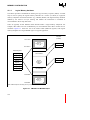
1
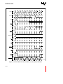
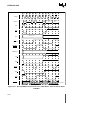
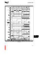
6.2.58
6.2.59
6.2.60
6.2.61
6.2.62
6.2.63
6.2.64
6.2.65
6.2.66
6.2.67
6.2.68
6.2.69
SEL<cc> ................................................................................................................ 6-97
setbit ...................................................................................................................... 6-99
SHIFT .................................................................................................................. 6-100
spanbit ................................................................................................................. 6-103
STORE ................................................................................................................ 6-104
subc ..................................................................................................................... 6-108
SUB<cc> ............................................................................................................. 6-109
subi, subo ............................................................................................................ 6-112
syncf .................................................................................................................... 6-113
sysctl .................................................................................................................... 6-114
TEST<cc> ............................................................................................................ 6-118
xnor, xor ............................................................................................................... 6-120
CHAPTER 7
PROCEDURE CALLS
7.1
CALL AND RETURN MECHANISM .............................................................................. 7-2
7.1.1
Local Registers and the Procedure Stack ............................................................... 7-2
7.1.2
Local Register and Stack Management ................................................................... 7-4
7.1.2.1
Frame Pointer ................................................................................................... 7-4
7.1.2.2
Stack Pointer .................................................................................................... 7-4
7.1.2.3
Considerations When Pushing Data onto the Stack ........................................ 7-4
7.1.2.4
Considerations When Popping Data off the Stack ........................................... 7-5
7.1.2.5
Previous Frame Pointer .................................................................................... 7-5
7.1.2.6
Return Type Field ............................................................................................. 7-5
7.1.2.7
Return Instruction Pointer ................................................................................. 7-5
7.1.3
Call and Return Action ............................................................................................. 7-5
7.1.3.1
Call Operation .................................................................................................. 7-6
7.1.3.2
Return Operation .............................................................................................. 7-7
7.1.4
Caching Local Register Sets ................................................................................... 7-7
7.1.4.1
Reserving Local Register Sets for High Priority Interrupts ............................... 7-8
7.1.5
Mapping Local Registers to the Procedure Stack .................................................. 7-11
7.2
MODIFYING THE PFP REGISTER............................................................................. 7-11
7.3
PARAMETER PASSING ............................................................................................. 7-12
7.4
LOCAL CALLS ............................................................................................................ 7-14
7.5
SYSTEM CALLS ......................................................................................................... 7-15
7.5.1
System Procedure Table ....................................................................................... 7-15
7.5.1.1
Procedure Entries ........................................................................................... 7-17
7.5.1.2
Supervisor Stack Pointer ................................................................................ 7-17
7.5.1.3
Trace Control Bit ............................................................................................ 7-17
7.5.2
System Call to a Local Procedure ......................................................................... 7-18
7.5.3
System Call to a Supervisor Procedure ................................................................. 7-18
7.6
USER AND SUPERVISOR STACKS .......................................................................... 7-19
7.7
INTERRUPT AND FAULT CALLS............................................................................... 7-19
7.8
RETURNS ................................................................................................................... 7-20
viii