1
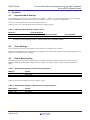
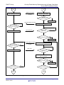
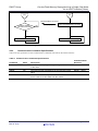
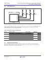
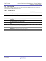
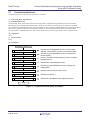
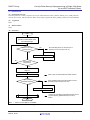
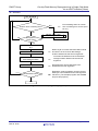
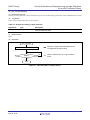
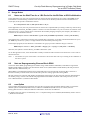
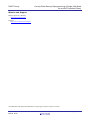
APPLICATION NOTE RX62T Group On-chip Flash Memory Reprogramming in Single-chip Mode via an UART Interface (Slave) R01AN0640EJ0102 Rev.1.02 Mar 04, 2015 Introduction This application note describes the write and erase processing for the flash memory (user MAT) using the erase block number, write data size, and write data transferred by asynchronous serial communication from an RX62T Group microcontroller (R01AN0639EJ) as described in “On-chip Flash Memory Reprogramming in Single-chip Mode via an UART Interface (Master)”. See the RX62T Group document “On-chip Flash Memory Reprogramming in Single-chip Mode via an UART Interface (Master)” (R01AN0639EJ) for details on the processing used to transfer the erase block number, write data size, and write data using asynchronous serial communication. Note that the erase and write processing for the internal flash memory used here is taken from the “RX600 Series Simple Flash API for RX600” application note Rev.2.20 (R01AN0544EU0220). Target Device RX62T Group This program can be used with other RX Family MCUs that have the same I/O registers (peripheral device control registers) as the RX62T Group. Check the latest version of the manual for any additions and modifications to functions. Careful evaluation is recommended before using this application note. Contents 1. Specifications .................................................................................................................................... 2 2. Operation Confirmation Environment ................................................................................................ 4 3. Functions Used ................................................................................................................................. 4 4. Operation ........................................................................................................................................... 5 5. Software Description ....................................................................................................................... 16 6. Usage Notes .................................................................................................................................... 38 7. Reference Documents..................................................................................................................... 39 R01AN0640EJ0102 Rev.1.02 Mar 04, 2015 Page 1 of 40 RX62T Group 1. On-chip Flash Memory Reprogramming in Single Chip Mode via an UART Interface (Slave) Specifications • This application note describes writing and erasing the user MAT using an RX62T Group R5F562TAADFP microcontroller in single-chip mode. • The slave receives the erase block number, write data size, and write data using asynchronous serial communication from the master, and performs the write and erase operations required on the user MAT. • The SCI channel 0 (SCI0) module is used for asynchronous serial communication between the master and the slave. • Asynchronous serial communication specifications Bit rate: 31,250 bps Data length: 8 bits Parity bits: none Stop bits: 1 bit • In this application note’s sample program, the slave erases the specified erase block (EB08: 16 KB) and writes the received 8 KB (256 bytes × 32) of write data to the erased block (EB08) starting at the start address of that block. Note that this application note’s specifications call for the program code to be allocated to EB00 and EB01 and for it not to be erased or overwritten. Therefore it is an error for the master to specify EB00 or EB01 as an erase block number. • Handshaking is used to control communication between the master and slave. After processing the data received from the master, the slave returns an [ACCEPTABLE] command (55h) to the master. The master starts the next serial transfer after receiving the [ACCEPTABLE] command from the slave. • When the slave completes the erase and write processing of the user MAT normally, it reports this normal completion using the 4 LEDs connected to the I/O ports. It also reports the error state if an error occurs during communication with the master or during the write/erase processing. Figure 1 shows the specifications of the system used in this application note. Slave Master Asynchronous serial communication Write data transmission Write data (8 KB) [ACCEPTABLE] command (55h) Programming/ erasing of slave starts when the IRQ switch is pressed. IRQ I/O ports RX62T On-chip RAM EB08 Write data (8 KB) After EB08 is erased, the received write data is written to EB08 (in 256-byte units), beginning from the start address EB08 Unused area (8 KB) IRQ switch LED×4 Normal end indication or error end indication I/O ports RX62T LED×4 Normal end indication or error end indication Figure 1 Specifications R01AN0640EJ0102 Rev.1.02 Mar 04, 2015 Page 2 of 40 RX62T Group On-chip Flash Memory Reprogramming in Single Chip Mode via an UART Interface (Slave) Figure 2 shows a hardware configuration diagram of the slave device as used in this application note. Asynchronous serial communication* Master TxD0 RxD0 Slave P71 LED0 P72 LED1 P73 LED2 P33 LED3 MDE Endian switch MD1 MD0 Mode switch RES# Reset switch EXTAL XTAL 12.5 MHz crystal resonator TxD0 RxD0 +5.0 V VCC VSS RX62T RX62T Note: * The TxD0 and RxD0 pins of the slave are pulled up externally. Figure 2 Hardware Configuration Diagram of Slave Device R01AN0640EJ0102 Rev.1.02 Mar 04, 2015 Page 3 of 40 RX62T Group 2. On-chip Flash Memory Reprogramming in Single Chip Mode via an UART Interface (Slave) Operation Confirmation Environment Table 1 lists the environment required for confirming slave operation. Table 1 Slave Operation Confirmation Environment Item Device Description RX62T Group: R5F562TAADFP (ROM: 256 KB, RAM: 16 KB) Renesas Starter Kit (Under development as of February 21, 2012) 5.0 V 12.5 MHz (ICLK = 100 MHz, PCLK = 50 MHz) Room temperature Version 4.09.00.007 Board Power supply voltage Input clock Operating temperature High-performance Embedded Workshop Toolchain RX Standard Toolchain (V.1.2.0.0) Debugger/Emulator E1 Emulator Debugger component RX E1/E20 SYSTEM V.1.02.00 Optimizing linkage editor -rom=D=R,D_1=R_1,D_2=R_2,PFRAM=RPFRAM (rom option)* Note: * See 6.3, rom Option, for details. 3. • • • • • • Functions Used Clock generation circuit Low Power Consumption Interrupt control unit I/O ports Serial Communications Interface ROM (flash memory for code storage) For details, see the User’s Manual listed in 7, Reference Documents. R01AN0640EJ0102 Rev.1.02 Mar 04, 2015 Page 4 of 40 RX62T Group 4. 4.1 On-chip Flash Memory Reprogramming in Single Chip Mode via an UART Interface (Slave) Operation Operation Mode Settings In the sample program, the slave’s mode pins are set to MD1 = 1, MD0 = 1 to select single-chip mode as the operating mode, the ROME bit in system control register 0 (SYSCR0) is set to 1 to enable the on-chip ROM. The slave is activated from the user MAT in single-chip mode. Table 2 lists the slave operating mode settings used in the sample program. Table 2 Operating Mode Settings of Slave Device Mode Pin SYSCR0 Register MD1 MD0 ROME Operating Mode On-Chip ROM 1 1 1 Single-chip mode Enabled Note: The initial setting of the ROME bit in the SYSCR0 register is SYSCR0.ROME = 1, so it is not necessary for the sample program to make settings to the SYSCR0 register. 4.2 Clock Settings The evaluation board used for this application note includes a 12.5 MHz crystal oscillator. Therefore this application note uses the following settings for the system clock (ICLK) and the peripheral module clock (PCLK): 8× (100 MHz) and 4× (50 MHz). 4.3 Endian Mode Setting The sample program presented in this application note supports both big- and little-endian mode. Table 3 lists the hardware (MDE pin) endian mode settings of the slave device. Note that the master and slave endian settings must match. Table 3 Endian Mode Settings of Slave Device (Hardware) MDE pin 0 1 Endian Little endian Big endian Table 4 lists the endian settings used in the compiler options. Table 4 Endian Mode Settings of Slave Device (Compiler Options) MCU Option Endian endian = little Little endian endian = big Big endian Note: Set the MDE bit to match the endian mode selected as a compiler option. R01AN0640EJ0102 Rev.1.02 Mar 04, 2015 Page 5 of 40 RX62T Group 4.4 On-chip Flash Memory Reprogramming in Single Chip Mode via an UART Interface (Slave) Asynchronous Serial Communication Specifications This application note uses asynchronous serial communication between the master and the slave to receive communication commands ([FSTART], [ERASE], [WRITE]), the erase block number, the write data size, and the write data itself. Note that the slave transmits the [ACCEPTABLE] command (55h) as a status command for handshaking. The used SCI0 TxD0 and RxD0 pins are each pulled up externally. Table 5 shows the specifications of the asynchronous serial communication used here. Table 5 Asynchronous Serial Communication Specifications Item Channel Communication mode Bit rate Data length Parity bit Stop bit Error 4.4.1 Description SCI channel 0 (SCI0) Asynchronous mode 31,250 bps (PCLK = 50 MHz) 8 bits None 1 bit Overrun error, framing error Communication Sequence Figures 3 to 6 show the communication sequence between master and slave. Master IRQ switch pressed? Slave No Yes [FSTART] command Issue [FSTART] command 1 byte of data received? No (1 byte) Yes [FSTART] command received? Yes No Error processing [ACCEPTABLE] command [ACCEPTABLE] command received? No (1 byte) Issue [ACCEPTABLE] command Yes M1 S1 Figure 3 Communication Sequence (1) R01AN0640EJ0102 Rev.1.02 Mar 04, 2015 Page 6 of 40 RX62T Group On-chip Flash Memory Reprogramming in Single Chip Mode via an UART Interface (Slave) S1 M1 [ERASE] command No 1 byte of data received? Issue [ERASE] command (1 byte) Yes [ERASE] command received? No Error processing Yes [ACCEPTABLE] command Issue [ACCEPTABLE] command [ACCEPTABLE] command received? No (1 byte) Yes Erase block number Transmit erase block number (1 byte) No 1 byte of data received? Yes Erase block number check NG Error processing OK Erase the block specified by the received erase block number Erase processing check NG OK Error processing [ACCEPTABLE] command Issue [ACCEPTABLE] command [ACCEPTABLE] command received? No (1 byte) Yes M2 S2 Figure 4 Communication Sequence (2) R01AN0640EJ0102 Rev.1.02 Mar 04, 2015 Page 7 of 40 RX62T Group On-chip Flash Memory Reprogramming in Single Chip Mode via an UART Interface (Slave) S2 M2 [WRITE] command Transmit [WRITE] command Receive 1 byte of data (1 byte) [WRITE] command received? Yes No Error processing [ACCEPTABLE] command Issue [ACCEPTABLE] command [ACCEPTABLE] command received? (1 byte) No Yes Write data size Transmit write data size (4 bytes) No 4 bytes of data received? Yes NG Write data size check OK Error processing [ACCEPTABLE] command Issue [ACCEPTABLE] command [ACCEPTABLE] command received? No (1 byte) Yes Write data Transmit write data (256 bytes) No 256 bytes of data received? Yes Write 256 bytes of received write data to user MAT Write processing check OK Write data transmit finished? No Write data receive finished? Yes NG Error processing No Yes S3 M3 Figure 5 Communication Sequence (3) R01AN0640EJ0102 Rev.1.02 Mar 04, 2015 Page 8 of 40 RX62T Group On-chip Flash Memory Reprogramming in Single Chip Mode via an UART Interface (Slave) S3 M3 [ACCEPTABLE] command [ACCEPTABLE] command received? No (1 byte) Issue [ACCEPTABLE] command Yes Normal end processing Normal end processing Figure 6 Communication Sequence (4) 4.4.2 Communication Command Specifications Table 6 lists the specifications of the communication commands sent between the master and slave. Table 6 Communication Command Specifications Command FSTART Value 10h ERASE WRITE 11h 12h ACCEPTABLE 55h Description Command to start programming/erasing of the user MAT of the slave Command to start erasing of the user MAT of the slave Command to start programming of the user MAT of the slave Status command used by the slave to inform the master that it is able to receive data from the master. R01AN0640EJ0102 Rev.1.02 Mar 04, 2015 Communication Direction Master → slave Master → slave Master → slave Slave → master Page 9 of 40 RX62T Group 4.4.3 On-chip Flash Memory Reprogramming in Single Chip Mode via an UART Interface (Slave) Erasure Block Number After receiving an [ERASE] command from the master, the slave receives 1 byte of erasure block number (1 byte of data defined by a symbolic constant). Figure 7 shows the specifications of the erasure block number. See section 4.5.1, User MAT Erase Processing, for details on the erase block numbers. Erasure block number (unsigned char type) b7 b6 b5 b4 b3 b2 b1 b0 BD7 BD6 BD5 BD4 BD3 BD2 BD1 BD0 In this application note, a value corresponding to EB08 is used as the erase block number to write or erase the slave erase block EB08. Note: A value corresponding to EB02 to EB21 must be specified as the erase block number. If a value other than an erase block number is specified, the slave will recognize an error and perform error handling. Figure 7 Erasure Block Number Specifications 4.4.4 Write Data Size After receiving a [WRITE] command from the master, the slave receives 4 bytes of write data size. Figure 8 shows the specifications of the write data size. Write data size (unsigned long type) b31 b30 b29 b28 b27 b26 b25 b24 SZ31 SZ30 SZ29 SZ28 SZ27 SZ26 SZ25 SZ24 b23 b22 b21 b20 b19 b18 b17 b16 SZ23 SZ22 SZ21 SZ20 SZ19 SZ18 SZ17 SZ16 b15 b14 b13 b12 b11 b10 b9 b8 SZ15 SZ14 SZ13 SZ12 SZ11 SZ10 SZ09 SZ08 b7 b6 b5 b4 b3 b2 b1 b0 SZ07 SZ06 SZ05 SZ04 SZ03 SZ02 SZ01 SZ00 The sample program uses a write size of 8 KB, so the write data size value is [0000 2000h]. Notes: 1. The write data size must be greater than zero and less than or equal to the erase block size for the specified erase block. If 0 or a value greater than the erase block size is specified, the slave will recognize an error and perform error handling. 2. The size of write data transmissions is fixed at 256 bytes. Consequently, if the write data size specifies a value that is not a multiple of 256 bytes, the master transmits write data in units of 256 bytes and then fills in the final unit of write data, which is less than 256 bytes, with bytes of value FFh as padding to reach a total of 256 bytes, which it transmits to the slave. Figure 8 Write Data Size Specifications R01AN0640EJ0102 Rev.1.02 Mar 04, 2015 Page 10 of 40 RX62T Group 4.4.5 On-chip Flash Memory Reprogramming in Single Chip Mode via an UART Interface (Slave) Handshaking Control The slave uses handshaking with the master for communications control. The handshaking control used here consists of the slave first receiving a serial communication from the master, then performing the processing for the received data, and finally returning an [ACCEPTABLE] command (55h) when it is ready to receive the next serial communication. The master only starts the next serial communication after it has received an [ACCEPTABLE] command from the slave. 4.4.6 Overrun Error In this application note, if an overrun error occurs during slave asynchronous serial communication reception (the SCI0.SSR.ORER bit is set to 1), the slave will perform error handling. 4.4.7 Framing Error In this application note, if a framing error occurs during slave asynchronous serial communication reception (the SCI0.SSR.FER bit is set to 1), the slave will perform error handling. R01AN0640EJ0102 Rev.1.02 Mar 04, 2015 Page 11 of 40 RX62T Group 4.5 On-chip Flash Memory Reprogramming in Single Chip Mode via an UART Interface (Slave) User MAT Write and Erase See the “RX600 Simple Flash API” application note listed in section 7, Reference Documents, for details on the RX600 Simple Flash API used for write and erase in this application note. 4.5.1 User MAT Erase Processing The R_FlashErase() function provided by the RX600 Simple Flash API is used for user MAT erase processing. Therefore the block numbers for erasing are the same as the values specified to the R_FlashErase() function. Erase errors are indicated in the return value from the R_FlashErase() function. 4.5.2 User MAT Write Processing The R_FlashWrite() function provided by the RX600 Simple Flash API is used for user MAT write processing. Write errors are indicated in the return value from the R_FlashWrite() function. 4.5.3 Changes to the Simple Flash API The Simple Flash API r_flash_api_rx600_config.h file is modified for this application note. Table 7 lists the changes to r_flash_api_rx600_config.h. Table 7 Changes to r_flash_api_rx600_config.h Item Changed Changes to Simple Flash API settings 4.5.4 Place Changed //#define IGNORE_LOCK_BITS //#define COPY_CODE_BY_API //#define FLASH_API_USE_R_BSP Notes on Using Interrupts Flash ROM cannot be access during ROM write or erase operations. Therefore it is necessary to prevent access to the ROM by interrupts that occur during write or erase operations. Although interrupts are not used in this application note, this sample program includes code that suppresses interrupts, but that code is commented out. This sample interrupt suppression code is shown below. /* Holds IPL of processor before flash operation */ // static unsigned char flash_pipl; /* Save current processor IPL */ // flash_pipl = get_ipl(); /* If your system is using the interrupt, Enable this line. */ /* Set the processor IPL so that interrupts that access ROM will not occur during ROM program/erase operations. */ // set_ipl(FLASH_READY_IPL); /* If your system is using the interrupt, Enable this line. */ /* Erasure process by using "simple API" */ fcu_status = R_FlashErase((uint8_t)target_eb); /* Programming process by using "simple API" */ fcu_status = R_FlashWrite((uint32_t)fcu_info.p_write_adrs_now, (uint32_t)wrdata_buffer,BUF_SIZE); /* Program 256 byte data to the target EB by using "simpleAPI" * (call of R_FlashWrite function in "simpleAPI") */ /* Restore processor IPL */ // set_ipl(flash_pipl); /* If your system is using the interrupt, Enable this line. */ R01AN0640EJ0102 Rev.1.02 Mar 04, 2015 Page 12 of 40 RX62T Group 4.6 On-chip Flash Memory Reprogramming in Single Chip Mode via an UART Interface (Slave) LED Connections Figure 9 shows the connections of the slave I/O ports and LED0 to LED3. +5.0 V +5.0 V +5.0 V +5.0 V Slave LED3 LED2 LED1 LED0 P33 P73 P72 P71 RX62T Figure 9 Slave Device LED Connection Diagram As shown in figure 9, high-level output from an I/O port (P71, P72, P73, or P33) causes the corresponding LED among LED0 to LED3 to turn off, and low-level output causes the corresponding LED to illuminate. Table 8 shows the correspondence between I/O port output and LED states. Table 8 Slave I/O Port Output and LED States I/O Port P71 P72 P73 P33 4.7 Register Setting PORT7.DR.B1 = 1, PORT7.DDR.B1 = 1 PORT7.DR.B1 = 0, PORT7.DDR.B1 = 1 PORT7.DR.B2 = 1, PORT7.DDR.B2 = 1 PORT7.DR.B2 = 0, PORT7.DDR.B2 = 1 PORT7.DR.B3 = 1, PORT7.DDR.B3 = 1 PORT7.DR.B3 = 0, PORT7.DDR.B3 = 1 PORT3.DR.B3 = 1, PORT3.DDR.B3 = 1 PORT3.DR.B3 = 0, PORT3.DDR.B3 = 1 I/O Port State High-level output Low-level output High-level output Low-level output High-level output Low-level output High-level output Low-level output LED State LED0 Off On LED1 Off On LED2 Off On LED3 Off On Normal End Processing When programming/erasing of the user MAT completes successfully, the slave makes a normal end indication by means of four LEDs connected to the device. The normal end indication consists of LED0 to LED3 illuminating one after another in a sequence that is repeated multiple times. R01AN0640EJ0102 Rev.1.02 Mar 04, 2015 Page 13 of 40 RX62T Group 4.8 On-chip Flash Memory Reprogramming in Single Chip Mode via an UART Interface (Slave) Error Handling Table 9 lists the slave device errors that apply to the sample program. Error handling consists of indicating the error state by means of four LEDs connected to the device. Table 9 List of Slave Errors Error No. Error No. 01 Description An overrun or framing error occurred. Error No. 02 In the [FSTART] command wait state, the command received from the master was not an FSTART command. In the [ERASE] command wait state, the command received from the master was not an ERASE command. The erasure block data received from the master specifies a block other than EB02 to EB21. An error occurred in the erase processing for the erase block. In the [WRITE] command wait state, the command received from the master was not an [WRITE] command. The write data size received from the master was 0 or a value greater than the block size of the specified erase block. An error occurred in the data write processing. Error No. 03 Error No. 04 Error No. 05 Error No. 06 Error No. 07 Error No. 08 R01AN0640EJ0102 Rev.1.02 Mar 04, 2015 LED Indication LED3 LED2 LED1 Off Off Off LED0 On Off Off On Off Off Off On On Off On Off Off Off On Off On Off On On Off Off On On On On Off Off Off Page 14 of 40 RX62T Group 4.9 On-chip Flash Memory Reprogramming in Single Chip Mode via an UART Interface (Slave) Section Settings Table 10 shows the section settings for the slave device. Table 10 Section Settings of Slave Device Section RPFRAM Start Address 0000 0000h B_1 R_1 B_2 R_2 B R SI PResetPRG P PIntPRG C_1 C_2 C C$* 0000 1000h D_1 D_2 D W* PFRAM FIXEDVECT FFFF E000h FFFF E800h FFFF F000h FFFF FFD0h R01AN0640EJ0102 Rev.1.02 Mar 04, 2015 Description Area mapped in RAM as the [PFRAM] section by the ROM support option. Uninitialized data area (ALIGN = 1) Area mapped in RAM as the [D-1] section by the ROM support option. Uninitialized data area (ALIGN = 2) Area mapped in RAM as the [D-2] section by the ROM support option. Uninitialized data area (ALIGN = 4) Area mapped in RAM as the [D] section by the ROM support option. Interrupt stack area Program area (PowerON_Reset_PC program) Program area Program area (interrupt program) Constant area (ALIGN = 1) Constant area (ALIGN = 2) Constant area (ALIGN = 4) Section initialization table of uninitialized data area, relocatable vector area Initialized data area (ALIGN = 1) Initialized data area (ALIGN = 2) Initialized data area (ALIGN = 4) Switch statement branch table area (ALIGN = 4) Program area (user MAT programming/control program) Fixed vector area Page 15 of 40 RX62T Group 5. 5.1 On-chip Flash Memory Reprogramming in Single Chip Mode via an UART Interface (Slave) Software Description File Structure Table 11 shows the file structure of the slave device. In addition to the files listed in table 11, some files generated automatically by High-performance Embedded Workshop are used as well. Table 11 File Structure of Slave Device File Name 1 resetprg.c* main.c Description Initial settings This program handles the following operations: reception and transmission control for communication commands using asynchronous serial communication with the master; reception control for the erase block number, the write data size, and the write data; control of LED display at normal completion and when an error occurs. r_flash_api_rx600.c The Simple Flash API program 2 r_flash_api_rx600.h External reference include file for the Simple Flash API program* 2 r_flash_api_rx600_private.h External reference include file for the Simple Flash API program* 2 r_flash_api_rx600_config.h Simple Flash API parameter settings include header file* 2 mcu_info.h Simple Flash API parameter settings include header file* Notes: 1. This file is generated automatically by High-performance Embedded Workshop. In the sample program it has been edited to restore a line in the PowerON_Reset_PC function calling the HardwareSetup function, which was originally commented out. In the edited version the HardwareSetup function in the main.c file is called from the PowerON_Reset_PC function. 2. See the Simple Flash API application note for details. R01AN0640EJ0102 Rev.1.02 Mar 04, 2015 Page 16 of 40 RX62T Group 5.2 On-chip Flash Memory Reprogramming in Single Chip Mode via an UART Interface (Slave) Function Structure Table 12 lists the functions for the slave device and figure 10 shows the hierarchy of these functions. Table 12 Slave Device Functions Function PowerON_Reset_PC HardwareSetup main Flash_Update File Name resetprg.c main.c main.c main.c R_FlashErase R_FlashWrite Indicate_Ending_LED Indicate_Error_LED SCI_Rcv1byte SCI_Rcvnbyte SCI_Trs1byte r_flash_api_rx600.c r_flash_api_rx600.c main.c main.c main.c main.c main.c Description Initial settings function MCU initial settings function Main function Data send/receive control and error handling control functions User MAT erase control function User MAT programming control function Normal end processing function Error end processing function 1 byte data reception function n byte data reception function 1 byte data transmission function PowerON_Reset_PC HardwareSetup main Flash_Update R_FlashErase R_FlashWrite Indicate_Ending_LED Indicate_Error_LED SCI_Rcv1byte SCI_Rcvnbyte SCI_Trs1byte Figure 10 Hierarchy of Slave Device Functions R01AN0640EJ0102 Rev.1.02 Mar 04, 2015 Page 17 of 40 RX62T Group 5.3 On-chip Flash Memory Reprogramming in Single Chip Mode via an UART Interface (Slave) Symbolic Constants Table 13 lists the symbolic constants used by the slave device. Table 13 Symbolic Constants of Slave Device Symbolic Constant FSTART ERASE WRITE ACCEPTABLE Setting Value 0x10 0x11 0x12 0x55 LED_ON 0 LED_OFF 1 RSK_LED0 PORT7.DR.BIT.B1 RSK_LED1 PORT7.DR.BIT.B2 RSK_LED2 PORT7.DR.BIT.B3 RSK_LED3 PORT3.DR.BIT.B3 RSK_LED0_DDR PORT7.DDR.BIT.B1 RSK_LED1_DDR PORT7.DDR.BIT.B2 RSK_LED2_DDR PORT7.DDR.BIT.B3 RSK_LED3_DDR PORT3.DDR.BIT.B3 WAIT_SCI1BIT 1920 WAIT_LED 2000000 SIZE_WRITE_BLOCK 128 BUF_SIZE RxD0_ICR 256 PORTB.ICR.BIT.B1 R01AN0640EJ0102 Rev.1.02 Mar 04, 2015 Description Programming/erase start command Erase start command Programming start command Status command sent to the master Set value used when the LED is on Functions Used By main Flash_Update Flash_Update main Indicate_Ending_LED Indicate_Error_LED Set value used when the LED is off HardwareSetup Indicate_Ending_LED Indicate_Error_LED On/off control of LED 0 on the HardwareSetup evaluation board main Indicate_Ending_LED Indicate_Error_LED On/off control of LED 1 on the HardwareSetup evaluation board main Indicate_Ending_LED Indicate_Error_LED On/off control of LED 2 on the HardwareSetup evaluation board main Indicate_Ending_LED Indicate_Error_LED On/off control of LED 3 on the HardwareSetup evaluation board main Indicate_Ending_LED Indicate_Error_LED I/O control for LED 0 on the HardwareSetup evaluation board I/O control for LED 1 on the HardwareSetup evaluation board I/O control for LED 2 on the HardwareSetup evaluation board I/O control for LED 3 on the HardwareSetup evaluation board Standby time data used after HardwareSetup setting the SCI0 BRR register LED illumination interval data for Indicate_Ending_LED indication of successful completion Indicate_Error_LED of programming/erasing of slave user MAT Write size for programming user Flash_Update MAT (word units) Size of write data storage area Flash_Update RxD0 input buffer settings HardwareSetup Page 18 of 40 RX62T Group On-chip Flash Memory Reprogramming in Single Chip Mode via an UART Interface (Slave) Symbolic Constant ERROR_NO_01 ERROR_NO_02 ERROR_NO_03 ERROR_NO_04 ERROR_NO_05 ERROR_NO_06 ERROR_NO_07 ERROR_NO_08 WRITE_ADRS_TOP_16K Setting Value 1 2 3 4 5 6 7 8 0x00FC0000 WRITE_ADRS_TOP_4K 0x00FF8000 BLK_SIZE_16K 16 × 1024 BLK_SIZE_4K 4 × 1024 R01AN0640EJ0102 Rev.1.02 Mar 04, 2015 Description Data indicating error state Functions Used By Flash_Update Indicate_Error_LED Start address of the 16 KB block size area in the write/erase address space Start address of the 4 KB block size area in the write/erase address space The size of each of the blocks in EB08 to EB21 The size of each of the blocks in EB00 to EB07 Flash_Update Page 19 of 40 RX62T Group 5.4 On-chip Flash Memory Reprogramming in Single Chip Mode via an UART Interface (Slave) RAM Variables Table 14 lists the RAM variables used by the slave device. Table 14 RAM Variables of Slave Device Variable wrdata_buffer[BUF_SIZE] Description Array for storing 256 bytes of write data received from the slave (256 bytes) fcu_info ST_FCU_INFO Structure for storing FCU-related address information 1 (* ) used to program/erase the user MAT (28 bytes) p_write_buffer unsigned short * Address of write data storage area used when programming user MAT: 4 bytes p_command_adrs unsigned char * FCU command destination address (programming/erase address): 4 bytes p_erase_adrs unsigned short * Start address of erase target erasure block (programming/erase address): 4 bytes p_write_adrs_top unsigned short * Start address of programming target erasure block (programming/erase address): 4 bytes p_write_adrs_end unsigned short * End address of programming target erasure block (programming/erase address): 4 bytes p_write_adrs_now unsigned short * Programming target address (programming/erase address): 4 bytes eb_block_size unsigned long Block size of the target erase block: 4 bytes Note: 1. For details on the ST_FCU_INFO type, see 5.5, Structures. 5.5 Type unsigned char Structures Table 15 lists the specifications of the ST_FCU_INFO structure used by the slave device. Table 15 ST_FCU_INFO Structure Specifications Member p_write_buffer Type unsigned short * p_command_adrs p_erase_adrs unsigned char * unsigned short * p_write_adrs_top unsigned short * p_write_adrs_end unsigned short * p_write_adrs_now eb_block_size unsigned short * unsigned long R01AN0640EJ0102 Rev.1.02 Mar 04, 2015 Description Address of write data storage area used when programming user MAT FCU command destination address (programming/erase address) Start address of erase target erasure block (programming/erase address) Start address of programming target erasure block (programming/erase address) End address of programming target erasure block (programming/erase address) Programming target address (programming/erase address) Block size of the target erase block Page 20 of 40 RX62T Group 5.6 On-chip Flash Memory Reprogramming in Single Chip Mode via an UART Interface (Slave) I/O Registers The I/O registers of the slave device used by the sample program are listed below. Note that the setting values shown are those used in the sample program and differ from the initial setting values. (1) Clock Generation Circuit System Clock Control Register (SCKCR) Bit b11 to b8 b27 to b24 Symbol PCK[3:0] Setting Value 0001 ICK[3:0] 0000 Bit Name Peripheral module clock (PCLK) select bits System clock (ICLK) select bits (2) I/O Ports Port 7 Data Register (P7.DR) Bit b1 Symbol B1 b2 B2 b3 B3 Setting Value 0 1 0 1 0 1 Bit Name P71 output data storage bit P72 output data storage bit P73 output data storage bit Symbol B3 Setting Value 0 1 Port 7 Data Direction Register (P7.DDR) Bit b1 b2 b3 Symbol B1 B2 B3 Setting Value 1 1 1 Bit Name P71 I/O select bit P72 I/O select bit P73 I/O select bit Port 3 Data Direction Register (P3.DDR) Bit b3 Symbol B3 Setting Value 1 Bit Name P33 I/O select bit Port B Input Buffer Control Register (PB.ICR) Bit b1 Symbol B1 Setting Value Bit Name 1 PB1 input buffer control bit R01AN0640EJ0102 Rev.1.02 Mar 04, 2015 R/W R/W R/W Address: 0008 C027h Function 0: Output data = 0 1: Output data = 1 0: Output data = 0 1: Output data = 1 0: Output data = 0 1: Output data = 1 Number of Bits: 8 Bit Name P33 output data storage bit Address: 0008 0020h Function 0001: × 4 PCLK = 50 MHz 0000: × 8 ICLK = 100 MHz Number of Bits: 8 Port 3 Data Register (P3.DR) Bit b3 Number of Bits: 32 R/W R/W R/W R/W Address: 0008 C023h Function 0: Output data = 0 1: Output data = 1 Number of Bits: 8 R/W R/W Address: 0008 C007h Function 1: Output port 1: Output port 1: Output port Number of Bits: 8 R/W R/W R/W R/W Address: 0008 C003h Function 1: Output port Number of Bits: 8 R/W R/W Address: 0008 C06Bh Function 1: PB1 input buffer enabled R/W R/W Page 21 of 40 RX62T Group On-chip Flash Memory Reprogramming in Single Chip Mode via an UART Interface (Slave) (3) Low Power Consumption Module Stop Control Register B (MSTPCRB) Bit b31 Symbol MSTPB31 Number of Bits: 32 Setting Value Bit Name 0 Serial communication interface 0 module stop setting bit (4) Serial Communications Interface 0 (SCI0) SCI0 Serial Control Register (SCI0.SCR) Address: 0008 0014h Function 0: SCI0 module stop state canceled Number of Bits: 8 R/W R/W Address: 0008 8242h (Serial communication interface mode (SMIF bit in SCI0.SCMR = 0)) Bit b1, b0 Symbol CKE[1:0] Setting Value Bit Name 00 Clock enable bits b2 TEIE 0 b4 RE b5 TE b6 RIE 0 1 0 1 0 Transmit end interrupt enable bit Receive enable bit Transmit enable bit Receive interrupt enable bit 1 b7 TIE 0 1 Function (For asynchronous communication) 00: Internal baud rate generator The SCK0 pin is set to be an I/O port. 0: TEI0 interrupt disabled R/W 1 R/W* 0: 1: 0: 1: 0: R/W* Serial reception disabled Serial reception enabled Serial transmission disabled Serial transmission enabled RXI0 and ERI0 interrupts disabled 1: RXI0 and ERI0 interrupts enabled R/W 2 2 R/W* R/W 0: TXI0 interrupt disabled R/W 1: TXI0 interrupt enabled Notes: 1. Writing to these bits is possible only when the TE and RE bits are both cleared to 0. 2. A value of 1 may be written to either these bits only when the TE and RE bits are both cleared to 0. Also, 0 may be written to both the TE and RE bits after one of them has been set to 1. R01AN0640EJ0102 Rev.1.02 Mar 04, 2015 Transmit interrupt enable bit Page 22 of 40 RX62T Group On-chip Flash Memory Reprogramming in Single Chip Mode via an UART Interface (Slave) SCI0 Serial Mode Register (SCI0.SMR) Number of Bits: 8 Address: 0008 8240h (Serial communication interface mode (SMIF bit in SCI0.SCMR = 0)) Bit b1, b0 b2 Symbol CKS[1:0] MP Setting Value Bit Name 00 Clock select bit 0 Multiprocessor mode bit Function R/W 1 2 00: PCLK clock (n = 0)* R/W* 2 (Only in asynchronous R/W* communication mode) 0: Multiprocessor communication function disabled 2 b3 STOP 0 Stop bits length select bit (Only in asynchronous R/W* communication mode) 0: One stop bit 2 b5 PE 0 Parity enable bit (Only in asynchronous R/W* communication mode) Transmission 0: No parity bits Reception 0: Reception with no parity 2 b6 CHR 0 Character length bit (Only in asynchronous R/W* communication mode) 0: Transmission and reception with an 8-bit data length 2 b7 CM 0 Communication mode bit 0: Asynchronous mode R/W* Notes: 1. For information on n setting values, see the User’s Manual listed in 7, Reference Documents. 2. Writing to these bits is possible only when the TE and RE bits in SCI0.SCR are both cleared to 0 (serial transmission and serial reception both disabled). SCI0 Smart Card Mode Register (SCI0.SCMR) Number of Bits: 8 Address: 0008 8246h Setting Value Bit Name Function R/W 0 Smart card interface 0: Serial communication interface R/W* mode select bit mode b3 SDIR 0 Bit order selection bit 0: LSB-first transmission/reception R/W* Note: * Writing to this bit is possible only when the TE and RE bits in SCI0.SCR are both cleared to 0 (serial transmission and serial reception both disabled). Bit b0 Symbol SMIF SCI0 Bit Rate Register (SCI0.BRR) Bit b7 to b0 Symbol Setting Value 1 00110001* Number of Bits: 8 Address: 0008 8241h Function R/W 2 31h: Bit rate = 31,250 bps R/W* (When PCLK is 50 MHz) Notes: 1. For information on BRR setting values, see the User’s Manual listed in 7, Reference Documents. 2. While this register can be read at any time, it can only be written when both the SCI0.SCR.TE bit and the SCI0.SCR.RE bits are 0 (serial transmission disabled and serial reception disabled). R01AN0640EJ0102 Rev.1.02 Mar 04, 2015 Bit Name Page 23 of 40 RX62T Group On-chip Flash Memory Reprogramming in Single Chip Mode via an UART Interface (Slave) SCI0 Serial Status Register (SCI0.SSR) Number of Bits: 8 Address: 0008 8244h (Serial communication interface mode (SMIF bit in SCI0.SCMR = 0)) Bit b2 Symbol TEND Setting Value Bit Name Transmit end flag Function R/W 0: Character transmission in progress R 1: Character transmission finished 1 b4 FER * Framing error flag 0: No framing error occurred R/(W) 2 * 1: A framing error occurred 1 b5 ORER * Overrun error flag 0: No overrun error occurred R/(W) 2 * 1: An overrun error occurred Notes: 1. The FER and ORER bits are handled as read-only in this application note. Writing to these bits to clear the flags to 0 is not performed. 2. Only writing 0 to clear the flag is allowed. SCI0 Transmit Data Register (SCI0.TDR) Setting Bit Symbol Value Bit Name b7 to * b0 Note: * The transmitted data is stored in this field. SCI0 Receive Data Register (SCI0.RDR) Bit b7 to b0 Symbol Setting Value Bit Name (5) Interrupt Control Unit (ICU) Interrupt Priority Register 80 (IPR80) Bit b3 to b0 Symbol IPR[3:0] Setting Value Bit Name 0000 SCI0 Interrupt priority level setting bits Interrupt Request Enable Register 1A (IER1A) Bit b7 Symbol IEN7 Setting Value Bit Name 0 RXI0 Interrupt enable bit 7 Interrupt Request Enable Register 1B (IER1B) Bit b0 Symbol IEN0 Setting Value Bit Name 0 TXI0 Interrupt enable bit 0 R01AN0640EJ0102 Rev.1.02 Mar 04, 2015 Number of Bits: 8 Address: 0008 8243h Function Stores transmit data. Number of Bits: 8 R/W R/W Address: 0008 8245h Function Stores receive data. Number of Bits: 8 R/W R Address: 0008 7380h Function 0000: Level 0 (interrupt disabled) Number of Bits: 8 Address: 0008 721Ah Function 0: RXI0 interrupt disabled Number of Bits: 8 R/W R/W R/W R/W Address: 0008 721Bh Function 0: TXI0 interrupt disabled R/W R/W Page 24 of 40 RX62T Group On-chip Flash Memory Reprogramming in Single Chip Mode via an UART Interface (Slave) Interrupt Request Register 215 (IR215) Bit b0 Symbol IR Number of Bits: 8 Address: 0008 70D7h Setting Value Bit Name 0 RXI0 Interrupt status flag Function 0: No RXI0 interrupt request 1: RXI0 interrupt request Note: * Only 0 may be written to this bit to clear the flag. Writing 1 is prohibited. Interrupt Request Register 216 (IR216) Bit b0 Symbol IR Setting Value Bit Name 0 TXI0 Interrupt status flag Number of Bits: 8 Address: 0008 70D8h Function 0: No TXI0 interrupt request 1: TXI0 interrupt request Note: * Only 0 may be written to this bit to clear the flag. Writing 1 is prohibited. R01AN0640EJ0102 Rev.1.02 Mar 04, 2015 R/W R/W* R/W R/W* Page 25 of 40 RX62T Group 5.7 On-chip Flash Memory Reprogramming in Single Chip Mode via an UART Interface (Slave) Function Specifications The specifications of the slave device functions are as follows. (1) PowerON_Reset_PC Function (a) Functional Overview The PowerON_Reset_PC function initializes the stack pointer (a #pragma entry declaration causes the compiler automatically to generate ISP/USP initialization code at the start of the PowerON_Reset_PC function), sets INTB (set_intb function: embedded function), initializes FPSW (set_fpsw function: embedded function), initializes the RAM area section (_INITSCT function: standard library function), calls the HardwareSetup function, initializes PSW (set_psw function: embedded function), and sets user mode as the processor mode. Then it calls the main function. (b) Arguments None (c) Return Values None (d) Flowchart PowerON_Reset_PC set_intb Use the set_intb embedded function to set the start address of the [C$VECT] section in the INTB register. set_fpsw Use the set_fpsw embedded function to initialize the FPSW register. _INITSCT Use the _INITSCT standard library function to initialize the RAM section. HardwareSetup Call the MCU initial settings function. Use the set_psw embedded function to initialize the PSW register. set_psw Set processor mode main Set user mode as the processor mode. Call the main function. brk Call the brk embedded function (BRK instruction). End Figure 11 Flowchart (PowerON_Reset_PC) (Slave) R01AN0640EJ0102 Rev.1.02 Mar 04, 2015 Page 26 of 40 RX62T Group On-chip Flash Memory Reprogramming in Single Chip Mode via an UART Interface (Slave) (2) HardwareSetup Function (a) Functional Overview The HardwareSetup function makes initial settings to the MCU. It makes initial clock settings (system clock (ICLK) and peripheral module clock (PCLK), initial I/O settings for the I/O ports (P71, P72, P73, and P33) connected to LED0 to LED3, and initial settings to SCI0. (b) Arguments None (c) Return Values None (d) Flowchart HardwareSetup • System clock ICLK = 100 MHz • Peripheral module clock PCLK = 50 MHz Clock settings LED port initial I/O settings SCI0 initial settings End • LED0 (P71): Initial output = high (LED0: turning off) • LED1 (P72): Initial output = high (LED1: turning off) • LED2 (P73): Initial output = high (LED2: turning off) • LED3 (P33): Initial output = high (LED3: turning off) • Cancel SCI0 module stop state. • Disable transmit and receive operation. • Enable PB1/RxD0 input pin buffer. • Set PCLK clock as clock source of on-chip baud rate generator. • Set asynchronous mode as communication mode. • Set serial communication interface mode as SCI0 operating mode. • Set the bit rate to 31,250 bps (when PCLK = 50 MHz) • Set the data length to 8 bits • Set no parity bit • Set number of stop bits to 1 • Wait for a 1-bit period at the bit rate • Set the SCI0 interrupt priority level to interrupts disabled • Disable TXI0 and RXI0 interrupts. • Clear TXI0 and RXI0 interrupt status flags. Figure 12 Flowchart (HardwareSetup) (Slave) R01AN0640EJ0102 Rev.1.02 Mar 04, 2015 Page 27 of 40 RX62T Group On-chip Flash Memory Reprogramming in Single Chip Mode via an UART Interface (Slave) (3) main Function (a) Functional Overview The main() function controls reception of one byte of data from the master, calls the Indicate_Error_LED() function when an error occurs, and calls the user MAT write/control program (the Flash_Update() function) in internal RAM. (b) Arguments None (c) Return Values None (d) Flowchart main Enable SCI0 transmit and receive operation. Enable RXI0, ERI0, and TXI0 interrupts. NG Overrun error or framing error? Error handling when an overrun error or framing error occurs (error No. 01) OK Indicate_Error_LED No Reception of 1 byte done? Yes Clear RXI0 interrupt status flag to 0. Read 1 byte of receive data from RDR of SCI0. Read receive data from RDR [FSTART] command received? No Error handling when the received data is not an [FSTART] command (error No. 02) Yes Indicate_Error_LED Jump to the user MAT programming/erase control program (Flash_Update function) in on-chip RAM.* Flash_Update End Note: * See 6.3, rom Option, for details. Figure 13 Flowchart (main) (Slave) R01AN0640EJ0102 Rev.1.02 Mar 04, 2015 Page 28 of 40 RX62T Group On-chip Flash Memory Reprogramming in Single Chip Mode via an UART Interface (Slave) (4) Flash_Update Function (a) Functional Overview The Flash_Update() function controls reception of communication commands using asynchronous serial communications with the master, controls reception of erase block numbers, controls reception of the write data size, controls reception of the write data, controls transmission of the ACCEPTABLE command, calls the R_FlashErase() function when the user MAT is erased, calls the R_FlashWrite() function when the user MAT is written, calls the Indicate_Ending_LED() function when a user MAT write or erase completes normally, and calls the Indicate_Error_LED() function when an operation terminates with an error. (b) Arguments None (c) Return Values None (d) Flowchart Flash_Update SCI_Trs1byte Transmit [ACCEPTABLE] command (1 byte) SCI_Rcv1byte Receive 1 byte of data from master. ([ERASE] command) [ERASE] command received? No Error handling when the received data is not an [ERASE] command (error No. 03) Yes Indicate_Error_LED SCI_Trs1byte Transmit [ACCEPTABLE] command (1 byte) SCI_Rcv1byte Receive 1 byte of data from master. (erasure block number). NG Error check OK Check whether erasure block number is within range EB02 to EB21, and if out of range perform error handling (error No. 04). Indicate_Error_LED Initialize fcu_info Initialize fcu_info (RAM variable) according to received erasure block number. 1 Figure 14 Flowchart (Flash_Update) (1) (Slave) R01AN0640EJ0102 Rev.1.02 Mar 04, 2015 Page 29 of 40 RX62T Group On-chip Flash Memory Reprogramming in Single Chip Mode via an UART Interface (Slave) 1 Erase the erasure block specified by the erasure block data. R_FlashErase NG Error check If an error occurs when erasing the erasure block, perform error handling (error No. 05). OK Indicate_Error_LED SCI_Trs1byte Transmit [ACCEPTABLE] command. (1 byte) SCI_Rcv1byte Receive 1 byte of data from the master ([WRITE] command). [WRITE] command received? No Error handling when the received data is not an [WRITE] command (error No. 06) Yes Indicate_Error_LED SCI_Trs1byte Transmit [ACCEPTABLE] command. (1 byte) SCI_Rcvnbyte Receive 4 bytes of data from the master (write size data). NG Error check Error handling when the received write data size value is 0 or larger than the size of the specified erase block. (error No. 07) OK Indicate_Error_LED Initialize fcu_info (RAM variable) according to the received write size data. Initialize fcu_info 2 Figure 15 Flowchart (Flash_Update) (2) (Slave) R01AN0640EJ0102 Rev.1.02 Mar 04, 2015 Page 30 of 40 RX62T Group On-chip Flash Memory Reprogramming in Single Chip Mode via an UART Interface (Slave) 2 Initialize storage buffer for write data received from master (wrdata_buffer[]) with FFh. Transmit [ACCEPTABLE] command. (1 byte) Initialize wrdata_buffer[ ] SCI_Trs1byte SCI_Rcvnbyte Receive 256 bytes of data from the master (write data). R_FlashWrite Write 256 bytes of data. NG Error check OK If an error occurs when writing the 256 bytes of data, perform error handling (error No. 08). Indicate_Error_LED No Programming finished? Determine whether writing of the received write size data quantity is finished. Yes SCI_Trs1byte Transmit [ACCEPTABLE] command. (1 byte) Disable SCI0 transmit and receive operation. Disable RXI0, ERI0, and TXI0 interrupts. Indicate_Ending_LED Normal end processing Figure 16 Flowchart (Flash_Update) (3) (Slave) R01AN0640EJ0102 Rev.1.02 Mar 04, 2015 Page 31 of 40 RX62T Group On-chip Flash Memory Reprogramming in Single Chip Mode via an UART Interface (Slave) (5) Indicate_Ending_LED Function (a) Functional Overview When programing/erasing completes successfully, the Indicate_Ending_LED function indicates a normal end using LED0 to LED3. The function illuminates LED0 to LED3 one at a time in sequence. (b) Arguments None (c) Return Values None (d) Flowchart Indicate_Ending_LED LED0 on (LED1 to LED3 off) Wait (WAIT_LED) Wait processing using for loop (loop count: WAIT_LED) LED1 on (LED0, LED2, and LED3 off) Wait (WAIT_LED) Wait processing using for loop (loop count: WAIT_LED) LED2 on (LED0, LED1, and LED3 off) Wait (WAIT_LED) Wait processing using for loop (loop count: WAIT_LED) LED3 on (LED0 to LED2 off) Wait (WAIT_LED) Wait processing using for loop (loop count: WAIT_LED) End Figure 17 Flowchart (Indicate_Ending_LED) (Slave) R01AN0640EJ0102 Rev.1.02 Mar 04, 2015 Page 32 of 40 RX62T Group On-chip Flash Memory Reprogramming in Single Chip Mode via an UART Interface (Slave) (6) Indicate_Error_LED Function (a) Functional Overview When an error occurs during programing/erasing of the user MAT, the Indicate_Error_LED function indicates the error number using LED0 to LED3. The display alternates repeatedly between the error number indication and all LEDs off. (b) Arguments Table 16 lists the arguments used by this function. Table 16 Arguments of Indicate_Error_LED Function Arguments 1st argument Type unsigned char Description Error number* that occurred during programing/erasing of the user MAT Note: * For information on error numbers, see 4.8, Error Handling. (c) Return Values None (d) Flowchart Indicate_Error_LED Display error number (01 to 08) using LED0 to LED3 For a description of the indications of LED0 to LED3, see 4.8, Error Handling. Wait (WAIT_LED) Wait processing using for loop (loop count: WAIT_LED) LED0 to LED3 off Turn all of LED0 to LED3 off. Wait (WAIT_LED) Wait processing using for loop (loop count: WAIT_LED) End Figure 18 Flowchart (Indicate_Error_LED) (Slave) R01AN0640EJ0102 Rev.1.02 Mar 04, 2015 Page 33 of 40 RX62T Group On-chip Flash Memory Reprogramming in Single Chip Mode via an UART Interface (Slave) (7) SCI_Rcv1byte Function (a) Functional Overview The SCI_Rcv1byte function performs the reception control for receiving 1 byte of data over SCI0 asynchronous serial communication. (b) Arguments None (c) Return Values Table 17 lists the return values used by this function. Table 17 Return Values SCI_Rcv1byte Function Type unsigned char (d) Description The one byte of receive data from the SCI0 asynchronous serial communication. Flowchart SCI_Rcv1byte Overrun error or framing error? OK No Reception of 1 byte done? Error handling when an overrun error or framing error occurs (error No. 01) NG Indicate_Error_LED Reception of 1 byte finished? Yes Clear RXI0 interrupt status flag to 0. Read receive data from RDR Return receive data Read 1 byte of receive data from RDR of SCI0. Send 1 byte of receive data as return value. End Figure 19 Flowchart (SCI_Rcv1byte) (Slave) R01AN0640EJ0102 Rev.1.02 Mar 04, 2015 Page 34 of 40 RX62T Group On-chip Flash Memory Reprogramming in Single Chip Mode via an UART Interface (Slave) (8) SCI_Rcvnbyte Function (a) Functional Overview The SCI_Rcvnbyte function controls reception of n bytes of data (n is the first argument and unsigned short type) using asynchronous serial communication by SCI0. (b) Arguments Table 18 lists the arguments used by this function. Table 18 Arguments of SCI_Rcvnbyte Function Arguments 1st argument Type unsigned short 2nd argument unsigned char * Description Receive data byte count obtained using asynchronous serial communication by SCI0 Start address of receive data storage location (c) Return Values None R01AN0640EJ0102 Rev.1.02 Mar 04, 2015 Page 35 of 40 RX62T Group (d) On-chip Flash Memory Reprogramming in Single Chip Mode via an UART Interface (Slave) Flowchart SCI_Rcvnbyte Overrun error or framing error? Error handling when an overrun error or framing error occurs (error No. 01) NG OK Indicate_Error_LED No Reception of 1 byte done? Yes Clear RXI0 interrupt status flag to 0. Read receive data from RDR Read 1 byte of receive data from RDR of SCI0 and store it in the receive data storage location obtained as the second argument. Increment address of receive data storage location Increment the address of the receive data storage location obtained as the second argument. Decrement receive data count != 0 Receive data count? =0 Decrement the receive data byte count obtained as the first argument. Repeat the receive operation until the receive data byte count obtained as the first argument reaches 0. (The sample program uses a while loop for this purpose.) End Figure 20 Flowchart (SCI_Rcvnbyte) (Slave) R01AN0640EJ0102 Rev.1.02 Mar 04, 2015 Page 36 of 40 RX62T Group On-chip Flash Memory Reprogramming in Single Chip Mode via an UART Interface (Slave) (9) SCI_Trs1byte Function (a) Functional Overview The SCI_Trs1byte function controls transmission of one byte of data using asynchronous serial communication by SCI0. (b) Arguments Table 19 lists the arguments used by this function. Table 19 Arguments of SCI_Trs1byte Function Arguments 1st argument Type unsigned char Description Transmit data byte count obtained using asynchronous serial communication by SCI0 (c) Return Values None (d) Flowchart SCI_Trs1byte Write the 1 byte of transmit data from the 1st argument to TDR of SCI0. Write transmit data to TDR TEND ? =0 Wait for transmission of 1 byte of data to finish. =1 End Figure 21 Flowchart (SCI_Trs1byte) (Slave) R01AN0640EJ0102 Rev.1.02 Mar 04, 2015 Page 37 of 40 RX62T Group 6. 6.1 On-chip Flash Memory Reprogramming in Single Chip Mode via an UART Interface (Slave) Usage Notes Notes on the Wait Time for a 1-Bit Period for the Bit Rate at SCI0 Initialization In this application note, the 1-bit period wait time for the bit rate after setting the bit rate register (SCI0.BRR) at SCI initialization is measured using a software timer. Since the bit rate for SCI0 asynchronous serial communication is 31,250 bps, the bit period is calculated as follows. The 1-bit period for the 31,250 bps bit rate is: 32 µs. In this application note, the 1-bit period wait time for the bit rate is implemented by iterating a while loop with the loop count defined by the WAIT_SCI1BIT symbolic constant. If we take the number of cycles to execute one iteration of the while loop to be 5 cycles* (which can be verified from the assembly language output by the compiler), the number of iterations can be calculated as follows. while loop run count = wait duration / (cycle count per while loop iteration × ICLK cycle duration) Note that the CPU’s instruction processing time can differ due to pipelining, so the above-mentioned number of cycles per while loop iteration (5 cycles) is a rough estimate of the instruction processing time. In the sample program, the wait duration is calculated as 96 [µs] to provide a sufficient margin, as follows: while loop run count = = WAIT_SCI1BIT = 96 [µs] / (5 × 10 [ns]) = 1,920 (ICLK = 100 MHz) Therefore, the symbolic constant WAIT_ SCI1BIT is defined as 1,920. To use this application note, users should either carefully evaluate the CPU instruction execution time or use a timer to measure this time. Note: * The number of cycles value below is for reference. The actual value will vary according to the conditions of the user’s system. 6.2 Note on Reprogramming Erasure Block EB00 The erasure block EB00 (programming/erase address range: 00FF E000h to 00FF FFFF, read address range: FFFF E000h to FFFF FFFFh) contains areas allocated for fixed vectors (FFFF FF80h to FFFF FFFFh), ID code protection (FFFF FFA0h to FFFF FFAFh), etc. When EB00 is programmed/erased, the above-mentioned fixed vector and ID code protection data is erased. It is therefore necessary to make fixed vector and ID code protection settings again after erasing EB00. ID code protection is a function that disables programming and erasing by the host. ID code protection determinations are made by using a control code and ID code programmed in the ROM. For details of ID code protection, see the User’s Manual listed in 7, Reference Documents. 6.3 rom Option The procedure described in this application note uses the rom option of the optimizing linkage editor to relocate the defined symbols in PFRAM (ROM section) to addresses in RPFRAM (RAM section). As a result, after the Flash_Update function is called, the addresses in RAM are used as the run addresses. For details of the rom option, see RX Family C/C++ Compiler Package User’s Manual (REJ10J2062), listed in section 7, Reference Documents. R01AN0640EJ0102 Rev.1.02 Mar 04, 2015 Page 38 of 40 RX62T Group 7. On-chip Flash Memory Reprogramming in Single Chip Mode via an UART Interface (Slave) Reference Documents • User’s Manual RX62T Group User’s Manual: Hardware Rev.1.10 (The latest version can be downloaded from the Renesas Electronics Web site.) RX Family User’s Manual: Software Rev.1.00 (The latest version can be downloaded from the Renesas Electronics Web site.) • Development Environment Manual RX Family C/C++ Compiler Package User’s Manual Rev.1.01 (The latest version can be downloaded from the Renesas Electronics Web site.) • Application Note RX62T Group On-chip Flash Memory Reprogramming in Single-chip Mode via an UART Interface (Slave) (R01AN0639EJ) (The latest information can be downloaded from the Renesas Electronics Web site.) RX600 Series Simple Flash API for RX600 Rev.2.20 (R01AN0544EU) (The latest information can be downloaded from the Renesas Electronics Web site.) • Technical Updates (The latest information can be downloaded from the Renesas Electronics Web site.) R01AN0640EJ0102 Rev.1.02 Mar 04, 2015 Page 39 of 40 RX62T Group On-chip Flash Memory Reprogramming in Single Chip Mode via an UART Interface (Slave) Website and Support Renesas Electronics Website http://www.renesas.com/ Inquiries http://www.renesas.com/contact/ All trademarks and registered trademarks are the property of their respective owners. R01AN0640EJ0102 Rev.1.02 Mar 04, 2015 Page 40 of 40 Revision History Rev. 1.00 1.01 Date Sep 27, 2011 Mar 27, 2012 1.02 Mar 04, 2015 Description Page Summary — First edition issued 4 Table 1 Master Verified Operating Environment: evaluation environment updated. 11 4.5.3 Changes to the Simple Flash API: Changes to the RX600 Simple Flash API are now reflected in this section. 4.5.4 Notes on Using Interrupts: Added. 13 Table 10 Master Section Settings: Setting values modified. 14 Table 11 Master File Structure: RX600 Simple Flash API description modified. 15 Table 12 Slave Device Functions: Changes to the RX600 Simple Flash API are now reflected in this section. 37 Change to the version number of the RX600 Simple Flash API in section 7, Reference Documents, and removal of the R01AN0639EJ version number. — HEW workspace generated with the environment from table 1. 4 Table 1: Optimizing linkage editor added 4 Table 1: Note * added 28 Figure 13: Note * added 38 6.1: Note * added 38 6.3 rom Option added A-1 General Precautions in the Handling of MPU/MCU Products The following usage notes are applicable to all MPU/MCU products from Renesas. For detailed usage notes on the products covered by this document, refer to the relevant sections of the document as well as any technical updates that have been issued for the products. 1. Handling of Unused Pins Handle unused pins in accord with the directions given under Handling of Unused Pins in the manual. The input pins of CMOS products are generally in the high-impedance state. In operation with an unused pin in the open-circuit state, extra electromagnetic noise is induced in the vicinity of LSI, an associated shoot-through current flows internally, and malfunctions occur due to the false recognition of the pin state as an input signal become possible. Unused pins should be handled as described under Handling of Unused Pins in the manual. 2. Processing at Power-on The state of the product is undefined at the moment when power is supplied. The states of internal circuits in the LSI are indeterminate and the states of register settings and pins are undefined at the moment when power is supplied. In a finished product where the reset signal is applied to the external reset pin, the states of pins are not guaranteed from the moment when power is supplied until the reset process is completed. In a similar way, the states of pins in a product that is reset by an on-chip power-on reset function are not guaranteed from the moment when power is supplied until the power reaches the level at which resetting has been specified. 3. Prohibition of Access to Reserved Addresses Access to reserved addresses is prohibited. The reserved addresses are provided for the possible future expansion of functions. Do not access these addresses; the correct operation of LSI is not guaranteed if they are accessed. 4. Clock Signals After applying a reset, only release the reset line after the operating clock signal has become stable. When switching the clock signal during program execution, wait until the target clock signal has stabilized. When the clock signal is generated with an external resonator (or from an external oscillator) during a reset, ensure that the reset line is only released after full stabilization of the clock signal. Moreover, when switching to a clock signal produced with an external resonator (or by an external oscillator) while program execution is in progress, wait until the target clock signal is stable. 5. Differences between Products Before changing from one product to another, i.e. to a product with a different type number, confirm that the change will not lead to problems. The characteristics of an MPU or MCU in the same group but having a different part number may differ in terms of the internal memory capacity, layout pattern, and other factors, which can affect the ranges of electrical characteristics, such as characteristic values, operating margins, immunity to noise, and amount of radiated noise. When changing to a product with a different part number, implement a system-evaluation test for the given product. Notice 1. Descriptions of circuits, software and other related information in this document are provided only to illustrate the operation of semiconductor products and application examples. You are fully responsible for the incorporation of these circuits, software, and information in the design of your equipment. Renesas Electronics assumes no responsibility for any losses incurred by you or third parties arising from the use of these circuits, software, or information. 2. Renesas Electronics has used reasonable care in preparing the information included in this document, but Renesas Electronics does not warrant that such information is error free. Renesas Electronics 3. Renesas Electronics does not assume any liability for infringement of patents, copyrights, or other intellectual property rights of third parties by or arising from the use of Renesas Electronics products or assumes no liability whatsoever for any damages incurred by you resulting from errors in or omissions from the information included herein. technical information described in this document. No license, express, implied or otherwise, is granted hereby under any patents, copyrights or other intellectual property rights of Renesas Electronics or others. 4. You should not alter, modify, copy, or otherwise misappropriate any Renesas Electronics product, whether in whole or in part. Renesas Electronics assumes no responsibility for any losses incurred by you or 5. Renesas Electronics products are classified according to the following two quality grades: "Standard" and "High Quality". The recommended applications for each Renesas Electronics product depends on third parties arising from such alteration, modification, copy or otherwise misappropriation of Renesas Electronics product. the product's quality grade, as indicated below. "Standard": Computers; office equipment; communications equipment; test and measurement equipment; audio and visual equipment; home electronic appliances; machine tools; personal electronic equipment; and industrial robots etc. "High Quality": Transportation equipment (automobiles, trains, ships, etc.); traffic control systems; anti-disaster systems; anti-crime systems; and safety equipment etc. Renesas Electronics products are neither intended nor authorized for use in products or systems that may pose a direct threat to human life or bodily injury (artificial life support devices or systems, surgical implantations etc.), or may cause serious property damages (nuclear reactor control systems, military equipment etc.). You must check the quality grade of each Renesas Electronics product before using it in a particular application. You may not use any Renesas Electronics product for any application for which it is not intended. Renesas Electronics shall not be in any way liable for any damages or losses incurred by you or third parties arising from the use of any Renesas Electronics product for which the product is not intended by Renesas Electronics. 6. You should use the Renesas Electronics products described in this document within the range specified by Renesas Electronics, especially with respect to the maximum rating, operating supply voltage range, movement power voltage range, heat radiation characteristics, installation and other product characteristics. Renesas Electronics shall have no liability for malfunctions or damages arising out of the use of Renesas Electronics products beyond such specified ranges. 7. Although Renesas Electronics endeavors to improve the quality and reliability of its products, semiconductor products have specific characteristics such as the occurrence of failure at a certain rate and malfunctions under certain use conditions. Further, Renesas Electronics products are not subject to radiation resistance design. Please be sure to implement safety measures to guard them against the possibility of physical injury, and injury or damage caused by fire in the event of the failure of a Renesas Electronics product, such as safety design for hardware and software including but not limited to redundancy, fire control and malfunction prevention, appropriate treatment for aging degradation or any other appropriate measures. Because the evaluation of microcomputer software alone is very difficult, please evaluate the safety of the final products or systems manufactured by you. 8. Please contact a Renesas Electronics sales office for details as to environmental matters such as the environmental compatibility of each Renesas Electronics product. Please use Renesas Electronics products in compliance with all applicable laws and regulations that regulate the inclusion or use of controlled substances, including without limitation, the EU RoHS Directive. Renesas Electronics assumes no liability for damages or losses occurring as a result of your noncompliance with applicable laws and regulations. 9. Renesas Electronics products and technology may not be used for or incorporated into any products or systems whose manufacture, use, or sale is prohibited under any applicable domestic or foreign laws or regulations. You should not use Renesas Electronics products or technology described in this document for any purpose relating to military applications or use by the military, including but not limited to the development of weapons of mass destruction. When exporting the Renesas Electronics products or technology described in this document, you should comply with the applicable export control laws and regulations and follow the procedures required by such laws and regulations. 10. It is the responsibility of the buyer or distributor of Renesas Electronics products, who distributes, disposes of, or otherwise places the product with a third party, to notify such third party in advance of the contents and conditions set forth in this document, Renesas Electronics assumes no responsibility for any losses incurred by you or third parties as a result of unauthorized use of Renesas Electronics products. 11. This document may not be reproduced or duplicated in any form, in whole or in part, without prior written consent of Renesas Electronics. 12. Please contact a Renesas Electronics sales office if you have any questions regarding the information contained in this document or Renesas Electronics products, or if you have any other inquiries. (Note 1) "Renesas Electronics" as used in this document means Renesas Electronics Corporation and also includes its majority-owned subsidiaries. (Note 2) "Renesas Electronics product(s)" means any product developed or manufactured by or for Renesas Electronics. http://www.renesas.com SALES OFFICES Refer to "http://www.renesas.com/" for the latest and detailed information. Renesas Electronics America Inc. 2801 Scott Boulevard Santa Clara, CA 95050-2549, U.S.A. Tel: +1-408-588-6000, Fax: +1-408-588-6130 Renesas Electronics Canada Limited 9251 Yonge Street, Suite 8309 Richmond Hill, Ontario Canada L4C 9T3 Tel: +1-905-237-2004 Renesas Electronics Europe Limited Dukes Meadow, Millboard Road, Bourne End, Buckinghamshire, SL8 5FH, U.K Tel: +44-1628-585-100, Fax: +44-1628-585-900 Renesas Electronics Europe GmbH Arcadiastrasse 10, 40472 Düsseldorf, Germany Tel: +49-211-6503-0, Fax: +49-211-6503-1327 Renesas Electronics (China) Co., Ltd. Room 1709, Quantum Plaza, No.27 ZhiChunLu Haidian District, Beijing 100191, P.R.China Tel: +86-10-8235-1155, Fax: +86-10-8235-7679 Renesas Electronics (Shanghai) Co., Ltd. Unit 301, Tower A, Central Towers, 555 Langao Road, Putuo District, Shanghai, P. R. China 200333 Tel: +86-21-2226-0888, Fax: +86-21-2226-0999 Renesas Electronics Hong Kong Limited Unit 1601-1611, 16/F., Tower 2, Grand Century Place, 193 Prince Edward Road West, Mongkok, Kowloon, Hong Kong Tel: +852-2265-6688, Fax: +852 2886-9022 Renesas Electronics Taiwan Co., Ltd. 13F, No. 363, Fu Shing North Road, Taipei 10543, Taiwan Tel: +886-2-8175-9600, Fax: +886 2-8175-9670 Renesas Electronics Singapore Pte. Ltd. 80 Bendemeer Road, Unit #06-02 Hyflux Innovation Centre, Singapore 339949 Tel: +65-6213-0200, Fax: +65-6213-0300 Renesas Electronics Malaysia Sdn.Bhd. Unit 1207, Block B, Menara Amcorp, Amcorp Trade Centre, No. 18, Jln Persiaran Barat, 46050 Petaling Jaya, Selangor Darul Ehsan, Malaysia Tel: +60-3-7955-9390, Fax: +60-3-7955-9510 Renesas Electronics India Pvt. Ltd. No.777C, 100 Feet Road, HAL II Stage, Indiranagar, Bangalore, India Tel: +91-80-67208700, Fax: +91-80-67208777 Renesas Electronics Korea Co., Ltd. 12F., 234 Teheran-ro, Gangnam-Gu, Seoul, 135-080, Korea Tel: +82-2-558-3737, Fax: +82-2-558-5141 © 2015 Renesas Electronics Corporation. All rights reserved. Colophon 5.0