1
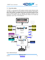
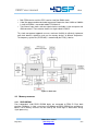
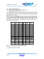
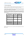
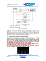
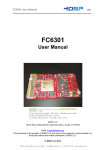
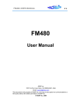
FM577 user manual
V1.2
FM577
User Manual
4DSP LLC, 955 S Virginia Street, Suite 214, Reno, NV 89502, USA
4DSP BV, Ondernemingsweg 66f, 2404HN, Alphen aan den Rijn, Netherlands
Email: [email protected]
This document is the property of 4DSP Inc. and may not be copied nor communicated to a
third party without the written permission of 4DSP Inc.
© 4DSP 2010
FM577 user manual
V1.2
Revision History
Date
Revision
Version
15-04-08
First release
1.0
15-05-08
Updated board images.
1.1
19-05-08
Removed obsolete information
1.1.1
May 12 2009
Changed logo, corrected typos
1.2
May 2010
FM577 User manual
www.4dsp.com
-2-
FM577 user manual
V1.2
Table of Contents
1
2
3
4
5
6
7
8
9
Acronyms and related documents ............................................................................. 4
1.1
Acronyms ............................................................................................................... 4
1.2
Related Documents ............................................................................................... 4
1.3
General description ................................................................................................ 5
Installation ................................................................................................................... 6
2.1
Requirements and handling instructions ................................................................ 6
2.2
Firmware and software........................................................................................... 6
Cyclone III features ...................................................................................................... 6
3.1
Series termination .................................................................................................. 6
Design .......................................................................................................................... 6
4.1
FPGA devices ........................................................................................................ 6
4.1.1
FPGA_A device.............................................................................................. 6
4.1.2
FPGA_B device.............................................................................................. 9
4.2
FPGA devices configuration ................................................................................... 9
4.2.1
Flash storage ................................................................................................. 9
4.2.2
CPLD device .................................................................................................10
4.2.3
JTAG .............................................................................................................12
4.3
Clock tree..............................................................................................................12
4.4
Memory resources ................................................................................................13
4.4.1
DDR2 SDRAM ..............................................................................................13
4.5
Front Panel IO daughter card ................................................................................14
4.5.1
Virtex-5 device to I/O front Panel daughter card ............................................14
4.5.2
Power connection to the front panel I/O daughter card ..................................16
Power requirements ...................................................................................................17
5.1
External power connector for stand alone mode ...................................................18
Environment................................................................................................................19
6.1
Temperature .........................................................................................................19
6.2
Convection cooling................................................................................................19
6.3
Conduction cooling ...............................................................................................19
Safety...........................................................................................................................19
EMC .............................................................................................................................19
Warranty ......................................................................................................................19
May 2010
FM577 User manual
www.4dsp.com
-3-
FM577 user manual
V1.2
1 Acronyms and related documents
1.1
Acronyms
ADC
DAC
DCI
DDR
DSP
EPROM
FBGA
FPDP
FPGA
JTAG
LED
LVTTL
LVDS
LSB
LVDS
MGT
MSB
PCB
PCI
PCI-e
PLL
PMC
QDR
SDRAM
SRAM
Analog to Digital Converter
Digital to Analog Converter
Digitally Controlled Impedance
Double Data Rate
Digital Signal Processing
Erasable Programmable Read-Only Memory
Fineline Ball Grid Array
Front Panel Data Port
Field Programmable Gate Array
Join Test Action Group
Light Emitting Diode
Low Voltage Transistor Logic level
Low Differential Data Signaling
Least Significant Bit(s)
Low Voltage Differential Signaling
Multi-Gigabit Transceiver
Most Significant Bit(s)
Printed Circuit Board
Peripheral Component Interconnect
PCI Express
Phase Locked Loop
PCI Mezzanine Card
Quadruple Data rate
Synchronous Dynamic Random Access memory
Synchronous Random Access memory
Table 1: Glossary
1.2
Related Documents
•
IEEE Std 1386.1-2001: IEEE Standard Physical and Environmental Layers for PCI
Mezzanine Cards (PMC).
PCI Special Interest Group (PCI SIG) PCI Local Bus Specification, Revision 3.0
•
•
•
•
ANSI/VITA 20-2001 : Conduction Cooled PMC.
ANSI/VITA 42.0-2005: XMC Switched Mezzanine Card Auxiliary Standard.
IEEE Std 1386-2001: IEEE Standard for a Common Mezzanine Card (CMC) Family.
Altera Cyclone III Device Handbook, Volume 1 and 2
•
May 2010
FM577 User manual
www.4dsp.com
-4-
FM577 user manual
1.3
V1.2
General description
The FM577 is a high performance PMC, optionally conduction cooled, dedicated to digital
signal processing applications with high bandwidth and complex algorithms requirements. It
offers multiple interfaces, fast on-board memory resources, and two Altera Cyclone III FPGA
devices. It can be utilized, for example, to accelerate frequency-domain algorithms with offthe-shelf Intellectual Property cores for applications that require the highest level of
performances. The FM577 is mechanically and electrically compliant to the standard and
specifications listed in section 1.2 of this document.
Optional
Front Panel IO
daughter card
Video, A/D, D/A, LVDS, Ethernet, etc
Optionally
conduction
cooled
114
DDR2
SDRAM
800MB/s
DDR2
SDRAM
800MB/s
Up to 512MB
Up to 512MB
DDR2
SDRAM
DDR2
SDRAM
800MB/s
800MB/s
EP3C120
Up to 512MB
Up to 512MB
EP3C40
SMA
External clock
output
FBGA 780
Configuration circuit
and JTAG
SMA
FPGA B
1PPS input or
external clock input
LED
x4
clocks
86
SMA
External clock
input
Flash
128Mbit
LED
Voltage and
temperature
monitoring
EP3C40
x4
EP3C16
FBGA 484
FPGA A
64 single ended
or
30 LVDS pairs
Pn1
Pn2
Pn3
Pn4
User I/O
PCI 66/33MHz 64/32-bit
Figure 1: FM577 block diagram
May 2010
FM577 User manual
www.4dsp.com
-5-
FM577 user manual
V1.2
2 Installation
2.1
Requirements and handling instructions
The FM577 must be installed on a motherboard compliant to the IEEE Std 1386-2001
standard for 3.3V PMC
Do not flex the board
Observe SSD precautions when handling the board to prevent electrostatic
discharges.
Do not install the FM4577 while the motherboard is powered up.
•
•
•
•
2.2
Firmware and software
Drivers, API libraries and a program example working in combination with a pre-programmed
firmware for both FPGAs are provided. The FM577 is delivered with an interface to the PCI
core in the FPGA_A device and an example VHDL design in the FPGA_B device so users
can start performing high bandwidth data transfers over the PCI bus right out of the box. For
more information about software installation and FPGA firmware, please refer the FM577 Get
Started Guide.
3 Cyclone III features
The Cyclone III devices offer features that simplify the PCB layout and improve signal
integrity.
3.1
Series termination
Cyclone III devices support on-chip series termination with calibration in all banks. The onchip series termination calibration circuit compares the total impedance of the I/O buffer to
the external resistors (50 ohms) connected to the RUP and RDN pins, and dynamically
adjusts the I/O buffer impedance until they match. This ensures limited reflections on the
data lines and better signal integrity. This feature will be used for the Pn4 interface as well as
for the PCI bus and the inter-FPGA bus.
4 Design
4.1
FPGA devices
The FPGA_A and FPGA_B FPGA devices interface to the various resources on the FM577
as shown on Figure 1. They also interconnect to each other via 82 general purpose pins and
4 clock pins (2 pairs, one in each direction, optionally 100Ω terminated).
4.1.1
4.1.1.1
FPGA_A device
Cyclone III device family and package
The FPGA_A device is from the Altera Cyclone III family. It can be an EP3C40 in a Fineline
Ball Grid array package with 484 balls.
May 2010
FM577 User manual
www.4dsp.com
-6-
FM577 user manual
4.1.1.2
V1.2
PCI interface
The FPGA_A device interfaces directly to the PCI bus via the PMC Pn1, Pn2 and Pn3
connectors. An embedded PCI core from Altera is used to communicate over the PCI bus
with the host system on the motherboard. PCI 64-bit 66MHz, PCI 64-bit 66MHz and PCI 32bit 33MHz are supported on the FM577. The bus type must be communicated at the time of
the order so the right FPGA_A device firmware can be loaded into the flash prior to delivery.
The following performances have been recorded with the FM577 transferring data on the
bus:
PCI 64-bit 66MHz: TBD
PCI 32-bit 33MHz: TBD
4.1.1.3
LED
Four LEDs are connected to the FPGA_A device. In the default FPGA firmware, the LEDs are
driven by the FPGA_B device via the inter-FPGA interface.
The LEDs are located on side 2 of the PCB in the front panel area.
FPGA_LED[3]
FPGA_LED[2]
FPGA_LED[1]
FPGA_LED[0]
Figure 2: FPGA LED locations
May 2010
FM577 User manual
www.4dsp.com
-7-
FM577 user manual
4.1.1.4
V1.2
Pn4 user I/O connector
The Pn4 connector is connected to the FPGA_A device. All 64 signals can be used as single
ended and Cyclone III series termination can be implemented. 3.3V, 2.5V or 1.8V signalling
is available (3.3V by default is mounted on board). Optionally LVDS signalling is available on
30 pairs, in which case the FPGA banks voltage must be set to 2.5V. The length skew
between any two data lines will not exceed 50mm. The following table gives the FPGA A pin
assignment for the Pn4 signals.
Connector
pin
1
3
5
7
9
11
13
15
17
19
21
23
25
27
29
31
33
35
37
39
41
43
45
47
49
51
53
55
57
59
61
63
May 2010
Signal
name
Pn4_IO0
Pn4_IO2
Pn4_IO4
Pn4_IO6
Pn4_IO8
Pn4_IO10
Pn4_IO12
Pn4_IO14
Pn4_IO16
Pn4_IO18
Pn4_IO20
Pn4_IO22
Pn4_IO24
Pn4_IO26
Pn4_IO28
Pn4_IO30
Pn4_IO32
Pn4_IO34
Pn4_IO36
Pn4_IO38
Pn4_IO40
Pn4_IO42
Pn4_IO44
Pn4_IO46
Pn4_IO48
Pn4_IO50
Pn4_IO52
Pn4_IO54
Pn4_IO56
Pn4_IO58
Pn4_IO60
Pn4_IO62
FPGA
pin
FPGA
pin
FM577 User manual
www.4dsp.com
Signal
name
Pn4_IO1
Pn4_IO3
Pn4_IO5
Pn4_IO7
Pn4_IO9
Pn4_IO11
Pn4_IO13
Pn4_IO15
Pn4_IO17
Pn4_IO19
Pn4_IO21
Pn4_IO23
Pn4_IO25
Pn4_IO27
Pn4_IO29
Pn4_IO31
Pn4_IO33
Pn4_IO35
Pn4_IO37
Pn4_IO39
Pn4_IO41
Pn4_IO43
Pn4_IO45
Pn4_IO47
Pn4_IO49
Pn4_IO51
Pn4_IO53
Pn4_IO55
Pn4_IO57
Pn4_IO59
Pn4_IO61
Pn4_IO63
Connector
pin
2
4
6
8
10
12
14
16
18
20
22
24
26
28
30
32
34
36
38
40
42
44
46
48
50
52
54
56
58
60
62
64
-8-
FM577 user manual
V1.2
Table 2 : Pn4 pin assignment
4.1.2
FPGA_B device
4.1.2.1
Cyclone III device family and package
The FPGA_B device is dedicated to Digital Signal Processing applications. This Altera
Cyclone III device can be either an EP3C120 in a Fineline Ball Grid array package with 780
balls.
4.1.2.2
Cyclone III device external memory interfaces
The FPGA_B device interfaces up to four 128Mbytes DDR2 SDRAM bank. A maximum
performance of up to 800MB/s per DDR2 SDRAM bank can be achieved.
4.1.2.3
Cyclone III device interface to Front Panel daughter card
The FPGA_B device interfaces to the front panel daughter card on the FM577 via a high
speed connector. 114 I/Os are available from the FPGA to/from the daughter card.
Refer to the Front Panel I/O section of this document for more details about the daughter
card connector electrical characteristics.
4.2
FPGA devices configuration
4.2.1 Flash storage
The FPGA firmware is stored on board in a flash device. The 512Mbit device is partly
used to store the configuration for both FPGAs. In the default CPLD firmware
configuration, the Cyclone III device A and B are directly configured from flash if a valid
bitstream is stored in the flash for each FPGA. The flash is pre-programmed in factory
with the default firmware example for both FPGAs.
May 2010
FM577 User manual
www.4dsp.com
-9-
FM577 user manual
V1.2
Figure 3 : Configuration circuit
4.2.2 CPLD device
As shown on Figure 2, a CPLD is connected between the flash device and the FPGA
devices. The CPLD main function is to program and read the flash. The data stored in the
flash are transferred from the host motherboard via the PCI bus to the FPGA_A device and
then to the CPLD writes the required bit stream to the storage device. A 31.25 MHz clock
connects to the CPLD and is used to generate the configuration clock sent to the FPGA
devices. At power up, if the CPLD detects that an FPGA configuration bitstream is stored in
the flash for both FPGA devices, it will start programming the devices.
Do NOT reprogram the CPLD without 4DSP approval
The CPLD configuration is achieved by loading with an Altera download cable a bitstream
from a host computer via the JTAG connector. The FPGA devices configuration can also be
performed using the JTAG.
4.2.2.1
DIP Switch
A switch (J1) is located next to the JTAG programming connector see Figure 4. The switch
positions are defined as follows:
May 2010
FM577 User manual
www.4dsp.com
- 10 -
FM577 user manual
V1.2
Figure 4: switch (J1) location
Sw1
OFF
Default setting. The Cyclone III device configuration is loaded from the flash at
power up.
ON
Cyclone III device safety configuration loaded from the flash at power up. To be
used only if the Cyclone III device cannot be configured or does not perform
properly with the switch in the OFF position.
Sw2
Reserved
Sw3
Reserved
Sw4
Reserved
Table 3: Switch description
4.2.2.2
LED and board status
Four LEDs connect to the CPLD and give information about the board status.
LED 0
LED 1
LED 2
LED 3
LED 3
Flashing
FPGA A or B bitstream or user_ROM_register is currently
being written to the flash
ON
FPGA A not configured
OFF
FPGA A configured
Flashing
FPGA A or B bitstream or user_ROM_register is currently
being written to the flash
ON
FPGA B not configured
OFF
FPGA B configured
Flashing
The FPGA_A device has been configured with the safety
configuration bitstream programmed in the flash at factory.
Please write a valid FPGA_A device bitstream to the flash.
ON
Flashn is busy writing or erasing
OFF
Flash device is not busy
ON
CRC error. Presumably a wrong or corrupted FPGA bitstream
has been written to the flash. Once on this LED remains on
OFF
No CRC error detected
Table 4: LED board status
May 2010
FM577 User manual
www.4dsp.com
- 11 -
FM577 user manual
V1.2
CPLD_LED[0]
CPLD_LED[1]
CPLD_LED[2]
CPLD_LED[3]
Figure 5: CPLD LED locations
4.2.3 JTAG
A JTAG connector is available on the FM577 for configuration purposes. The JTAG can also
be used to debug the FPGA design with the Altera Signal Tap.
The JTAG connector is located on side 1 of the PCB (see Figure 6).
Figure 6: JTAG connector location
The JTAG connector pinout is as follows:
Pin #
1
2
3
Signal
2.5V
GND
TCK
Signal
TMS
TDI
TDO
Pin #
4
5
6
Table 5 : JTAG pin assignment
4.3
Clock tree
The FM577 clock architecture offers an efficient distribution of low jitter clocks.
May 2010
FM577 User manual
www.4dsp.com
- 12 -
FM577 user manual
•
•
•
V1.2
Both FPGA devices and the CPLD receive a low jitter 50MHz clock.
A low jitter programmable clock able to generate frequencies from 16MHz to 230MHz
in steps of 0.5MHz is connected to both FPGA devices
Two external input clocks and one output clock are available via the front panel with
SMA connectors. These external clocks are single ended LVCMOS.
This clock management approach ensures maximum flexibility to efficiently implement
multi-clock domains algorithms and use the memory devices at different frequencies.
The frequency synthesizer (CDCEL925) is controlled by the FPGA_A device.
Figure 7 : Clock tree
4.4
Memory resources
4.4.1 DDR2 SDRAM
Four independent 16-bit DDR2 SDRAM banks are connected to FPGA B. Each bank
provides 128Mbytes. In total a maximum of 512Mbytes of DDR2 SDRAM are available on
board. These memory resources can be used by the FPGA logic as data buffers during
signal processing.
May 2010
FM577 User manual
www.4dsp.com
- 13 -
FM577 user manual
4.5
4.5.1
V1.2
Front Panel IO daughter card
Cyclone 3 device to I/O front Panel daughter card
(Only available with daughter card purchase)
The FPGA B interfaces to a 120-pin connector placed in the Front panel I/O area (on both
side 1 and side 2 of the PCB). It serves as a base for a daughter card and offers I/O diversity
to the FM577 PMC. On side 2 of the PCB, the connectors and mounting holes placement
complies with the SLB standard.
The FPGA I/O banks are powered either by 1.5V, 2.5V or 3.3V via large 0 ohms resistors
(3.3V is the default if not specified otherwise at the time of order). Please, contact 4DSP Inc.
for more information about the daughter card types available. The 120-pin Samtec connector
pin assignment is as follows. The pins are grouped in LVDS pairs (FP_Px and FP_Nx). All
signals that are shown as LVDS pairs in the table can be used for any standard that is not in
breach the Altera I/O pad electrical.
Connector
pin
1
3
5
7
9
11
13
15
17
19
21
23
25
27
29
31
Signal
Name
FP_P0
FP_N0
FP_P2(2)
FP_N2(2)
FP_P4
FP_N4
FP_P6
FP_N6
FP_P8
FP_N8
FP_P10(2)
(2)
FP_N10
FP_P12
FP_N12
FP_P14
FP_N14
33
35
37
39
FPGA
pin
FPGA
pin
Signal
name
FP_P1
FP_N1
FP_P3
FP_N3
FP_P5
FP_N5
FP_P7
FP_N7
FP_P9
FP_N9
FP_P11
FP_N11
FP_P13
FP_N13
FP_P15
FP_N15
Connector
pin
2
4
6
8
10
12
14
16
18
20
22
24
26
28
30
32
FP_P16(2)
FP_P17(1)
34
(2)
(1)
36
FP_N16
FP_N17
(1)
FP_P19
38
(1)
FP_N19
40
FP_P18
FP_N18
Table 6 : Front Panel IO daughter card pin assignment Bank A
(1)
(2)
Connected to a global clock pin on the FPGA.
Connected to a regional clock pin on the FPGA.
May 2010
FM577 User manual
www.4dsp.com
- 14 -
FM577 user manual
Connector
pin
41
43
45
47
49
51
53
55
57
59
61
63
65
67
69
71
73
75
77
79
81
83
85
87
89
91
93
95
97
99
101
103
105
107
109
111
113
115
117
119
Differential
FP_P20
FP_N20
FP_P22
FP_N22
FP_P24(2)
(2)
FP_N24
FP_P26
FP_N26
FP_P28
FP_N28
FP_P30
FP_N30
FP_P32
FP_N32
FP_P34
FP_N34
FP_P36(2)
3.3V/2.5V/1.8V
3.3V/2.5V/1.8V
3.3V/2.5V/1.8V
FP_P37
FP_N37
FP_P39
FP_N39
FP_P41
FP_N41
FP_P43
FP_N43
(1)
FP_P45
FP_N45(1)
FP_P47
FP_N47
FP_P49
FP_N49
FP_P51
FP_N51
FP_P53(2)
FP_N53(2)
FP_P55(1)
(1)
FP_N55
V1.2
FPGA
pin
FPGA
pin
Differential
FP_P21
FP_N21
FP_P23
FP_N23
FP_P25
FP_N25
FP_P27
FP_N27
FP_P29
FP_N29
FP_P31
FP_N31
FP_P33
FP_N33
(2)
FP_P35
FP_N35(2)
FP_N36(2)
Vbatt
0.9V
3.3V/2.5V/1.8V
FP_P38
FP_N38
FP_P40
FP_N40
FP_P42
FP_N42
FP_P44
FP_N44
FP_P46
FP_N46
FP_P48
FP_N48
FP_P50
FP_N50
FP_P52
FP_N52
FP_P54
FP_N54
FP_P56
FP_N56
Connector
pin
42
44
46
48
50
52
54
56
58
60
62
64
66
68
70
72
74
76
78
80
82
84
86
88
90
92
94
96
98
100
102
104
106
108
110
112
114
116
118
120
Table 7: Front Panel IO daughter card pin assignment Banks B and C
(1)
(2)
Connected to a global clock pin on the FPGA.
Connected to a regional clock pin on the FPGA.
May 2010
FM577 User manual
www.4dsp.com
- 15 -
FM577 user manual
V1.2
4.5.2 Power connection to the front panel I/O daughter card
The Front Panel I/O daughter card on side 1 of the PCB is powered via a 7-pin connector of
type BKS (Samtec). Each pin can carry up to 1.5A. The power connector’s pin assignment is
as follows.
Pin #
1
3
5
7
Signal
+3.3V
+5V
+12V
-12V
Signal
+3.3V
GND
GND
Pin #
2
4
6
Table 8: Daughter card power connector pin assignment on PMC side 1
On side 2 of the PCB, the daughter card is powered via a 33-pin connector of type BKS
(Samtec). Each pin can carry up to 1.5A. The power connector’s pin assignment is as
follows.
Pin #
1
3
5
7
9
11
13
15
17
19
21
23
25
27
29
31
33
Signal
+3.3V
+3.3V
+3.3V
+3.3V
+5V
+5V
+5V
+5V
+12V
+12V
-12V
-12V
GND
reserved
reserved
reserved
GND
Signal
GND
GND
GND
GND
GND
GND
GND
GND
GND
GND
GND
GND
reserved
reserved
reserved
reserved
Pin #
2
4
6
8
10
12
14
16
18
20
22
24
26
28
30
32
Table 9: Daughter card power connector pin assignment on PMC side 2
May 2010
FM577 User manual
www.4dsp.com
- 16 -
FM577 user manual
V1.2
5 Power requirements
The Power is supplied to the FM577 via the PMC. Several DC-DC converters generate the
appropriate voltage rails for the different devices and interfaces present on board.
The FM577 power consumption depends mainly on the FPGA devices work load. By using
high efficiency power converters, all care has been taken to ensure that power consumption
will remain as low as possible for any given application.
After power up the FM577 typically consumes 2W of power. For precise power
measurements it is recommended to use the Altera power estimation tools for both the
Cyclone III FPGA devices. The maximum current rating given in the table below is the
maximum current that can be drawn from each voltage rail in the case resources are used to
their maximum level.
Device/Interface
Voltage
Maximum
current rating
0.9V
100mA
FPGA A & B device core
1.2V
14A
DDR2 SDRAM core and I/O
banks, FPGA A & B devices I/O
banks
1.8V
8A
FPGA_A
device
I/O
bank
connected to the PCI bus, Flash,
CPLD, front Panel I/O daughter
card
3.0V/3.3V
3A
Front Panel IO daughter card
5V
1A
Front Panel IO daughter card
12V
0.5A
Front Panel IO daughter card
-12V
0.5A
Vref
and
memory
reference voltage
devices
Table 10 : Power supply
Optionally, the FM577 can be used as a stand alone module and is powered via the external
power connector.
May 2010
FM577 User manual
www.4dsp.com
- 17 -
FM577 user manual
V1.2
Figure 8 : Power supply
An ADT7411 device is used to monitor the power on the different voltage rails as well as the
temperature. The ADT7411 data are constantly passed to the Cyclone-III device.
Measurements can be accessed from the host computer via the PCI bus. A software utility
delivered with the board allows the monitoring of the voltage on the 2.5V, 1.8V, 1.5V, 1.0V
and 0.75V rails. It also displays both FPGAs junction temperature.
5.1
External power connector for stand alone mode
An external power connector (J2) is available on side 2 of the PMC, next to the PMC
connectors. It is used to power the board when it is in stand alone mode. This is a right
angled connector and it will be mounted on board only if the card is ordered as a stand alone
version (FM577-SA). The height and placement of this connector on the PCB breaches the
PMC specifications and the module should not be used in an enclosed chassis compliant to
PMC specifications if the external power connector is present on board.
Do not connect an external power source to J2 if the board is powered via the
PMC connectors. Doing so will result in damaging the board.
The external power connector is of type Molex 43045-1021. Each circuit can carry a
maximum current of 5A. The connector pin assignment is as follows:
Pin #
1
3
5
7
9
Signal
3.3V
5V
GND
GND
-12V
Signal
3.3V
5V
GND
GND
12V
Pin #
2
4
6
8
10
Table 11 : External power connector pin assignment
May 2010
FM577 User manual
www.4dsp.com
- 18 -
FM577 user manual
V1.2
6 Environment
6.1
Temperature
Operating temperature
• 0°C to +60°C (Commercial)
• -40°C to +85°C (Industrial)
Storage temperature:
• -40°C to +120°C
6.2
Convection cooling
300LFM minimum
6.3
Conduction cooling
The FM577 can optionally be delivered as conduction cooled PMC compliant to ANSI/VITA
20-2001 standard for conduction cooled PMC.
7 Safety
This module presents no hazard to the user.
8 EMC
This module is designed to operate from within an enclosed host system, which is build to
provide EMC shielding. Operation within the EU EMC guidelines is not guaranteed unless it
is installed within an adequate host system. This module is protected from damage by fast
voltage transients originating from outside the host system which may be introduced through
the system.
9 Warranty
Hardware
Software/Firmware
Basic Warranty (included)
1 Year from Date of Shipment
90 Days from Date of Shipment
Extended Warranty (optional)
2 Years from Date of Shipment
1 Year from Date of Shipment
May 2010
FM577 User manual
www.4dsp.com
- 19 -
FM577 user manual
V1.2
10 FM577 image
May 2010
FM577 User manual
www.4dsp.com
- 20 -