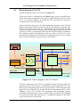
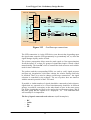
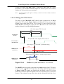
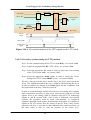
1
EUROPEAN ORGANIZATION FOR NUCLEAR RESEARCH
European Laboratory for Particle Physics
[Institute]
Internal Note/
ALICE reference number
[Institute address]
ALICE-INT-2003-056 version 1.0
Institute reference number
[-]
Date of last change
2002-10-15
Local Trigger Unit
Preliminary Design Review
Authors:
P. Jovanovic
for the ALICE Collaboration
Abstract:
This document is a compilation of texts used in proposals, replies, in technical discussions and
exchanges; above all, it is an edited version of the LTU working notes that have been
scrupulously updated throughout the progress of the project, in order to document the
development effort, to explain the ideas, the decisions, the reasons for and against, to serve as a
reminder.
Local Trigger Unit
PRELIMINARY DESIGN REVIEW
Revision 1.0 15 October 2002
Local Trigger Unit - Preliminary Design Review
ii
Local Trigger Unit - Preliminary Design Review
DOCUMENT HISTORY
Version
Date
Editor
Comments
Draft 0.1
01.09.02
P. Jovanovic
Version prepared for the LTU Preliminary Design
Review.
Version 1.0
15.10.02
P. Jovanovic
Decisions and recommendations from the LTU
Preliminary Design Review (10 and 11 October
2002, CERN) have been inserted in red.
Section 3.10.9, Error emulation, has been added.
This version has been presented to the ALICE
Technical Board for approval (22 October 2002).
iii
Local Trigger Unit - Preliminary Design Review
TABLE OF CONTENTS
1.0 INTRODUCTION ......................................................................................1
1.1 Preface .....................................................................................................1
1.2 Purpose and scope of the document ........................................................2
1.3 Document overview ................................................................................2
1.4 Definitions and acronyms........................................................................2
1.5 Signal name abbreviations ......................................................................4
1.6 References ...............................................................................................4
2.0 AT A GLANCE... .........................................................................................6
3.0 TECHNICAL SPECIFICATION ...............................................................9
3.1 Introduction .............................................................................................9
3.2 Layout of the ALICE trigger system.......................................................9
3.3 Context diagram of the LTU .................................................................11
3.4 Block diagram of the LTU ....................................................................13
3.5 LTU connections ...................................................................................14
3.5.1
3.5.2
3.5.3
3.5.4
3.5.5
3.5.6
3.6
Connections to the CTP ................................................................................... 14
Connections to the TTCvi board...................................................................... 17
Connection to the TTCex board....................................................................... 18
Connections to the sub-detector electronics.................................................... 18
Connection to the TTCit board ........................................................................ 19
LTU board front panel..................................................................................... 20
Use of the TTC system..........................................................................22
3.6.1
3.6.2
3.6.3
3.6.4
3.7
TTC address allocation.................................................................................... 22
Format of the L1 Message ............................................................................... 24
Format of the L2a Message ............................................................................. 25
Format of the L2r Word................................................................................... 26
Region of Interest interface ...................................................................26
3.7.1
3.7.2
3.8
RoII to TTC transmission................................................................................. 27
LTU to RoII interface....................................................................................... 27
LTU logic block ....................................................................................29
3.8.1
3.8.2
3.8.3
L1 Data and L2 Data de-serializers ................................................................ 30
Prevention of overflow of the TTCvi and the LTU FIFOs............................... 32
Control and arbitration of the FIFO read....................................................... 34
3.9 Generation of the BUSY signal.............................................................36
3.10
CTP emulator .....................................................................................37
3.10.1
3.10.2
3.10.3
3.10.4
3.10.5
3.10.6
3.10.7
List of emulation sequences ............................................................................. 37
Sequence List data ........................................................................................... 38
Sequence execution.......................................................................................... 40
Flow-chart of the sequence generation ........................................................... 42
Block diagram of the CTP emulator................................................................ 44
CTP emulator state machine - connections ..................................................... 46
Generation of the Start signal.......................................................................... 46
iv
Local Trigger Unit - Preliminary Design Review
3.10.8
3.10.9
3.11
3.12
3.13
3.14
3.14.1
3.14.2
3.14.3
3.14.4
3.14.5
3.14.6
3.14.7
3.14.8
3.14.9
3.14.10
3.14.11
3.14.12
LHC gap synchronisation circuit..................................................................... 49
Error emulation ............................................................................................... 50
Monitoring - scalers and timers .........................................................52
Snap-shot memory .............................................................................53
Oscilloscope probes ...........................................................................54
Timing considerations........................................................................56
System timing - general approach and main features ..................................... 56
Signal connections in the TTC partition.......................................................... 58
Timing of the TTCex board.............................................................................. 58
Timing of the TTCvi board .............................................................................. 61
Mutual timing of the CTP signals.................................................................... 62
L0 signal .......................................................................................................... 62
L1 signal .......................................................................................................... 63
Orbit signal...................................................................................................... 65
Pre-pulse signal ............................................................................................... 65
Re-synchronisation of data and strobe signals........................................... 65
Procedure of time-tuning the TTC partition............................................... 66
Automatic setting of the TTC partition timing - a proposal ....................... 67
v
Local Trigger Unit - Preliminary Design Review
vi
Local Trigger Unit - Preliminary Design Review
1.0
INTRODUCTION
1.1
Preface
This document is a compilation of texts used in proposals, replies, in technical
discussions and exchanges; above all, it is an edited version of the LTU
working notes that have been scrupulously updated throughout the progress of
the project, in order to document the development effort, to explain the ideas,
the decisions, the reasons for and against, to serve as a reminder.
As a whole, the document is a mess - inconsistent in details, too long, difficult
to read, without a natural flow, it branches chaotically in all directions, it’s
historical, it contemplates a plethora of options and versions, goes back to
battles won and lost...
It’s precious, nevertheless: it goes well beyond a mere presentation for a
conceptual design review of a single board; it’s a clear (clear?) overview of
the functionality the LTU board is expected to deliver; it deals with the system
issues and verifies the compatibility; it is pedantically detailed about some
aspects of time-tuning...
For us, working on the project, the document serves as a comprehensive highlevel design, the first step of the hierarchical top-down procedure we are going
to follow. When the project is complete, the text will be tidied up and slimmed
down to the format and size appropriate to the board documentation and a
proper User Manual.
An executive summery, re-named At a glance to avoid false flattery, is added
to help “fast readers”; they’ll find out that the document is about the LTU...
1
Local Trigger Unit - Preliminary Design Review
1.2
Purpose and scope of the document
This is a working document, currently in a draft form. Comments and
suggestions from the ALICE community are invited and encouraged. The
document shall be regularly updated, with changes explained in section
Document History.
The document gives a preliminary technical specification of the Local Trigger
Unit (LTU), based on a subset of requirements listed in the CTP URD [1]. The
document does not contain the design details since the design itself is not yet
done, but it studies the feasibility of the project and provides the guidelines for
the hardware implementation.
Since the project follows recommendations and guidelines of the ISO9001
structured quality management procedure [2], the preliminary specification
shall be assessed during the Preliminary Design Review in order to check that
the expected performance and functionality are met. The detailed design shall
be followed by the Final Design Review, before the prototype is produced and
tested; the Production Readiness Review shall be held before the final
production.
1.3
Document overview
The present section (Introduction) gives a brief account of the purpose and
scope of the document, explains its structure, defines terms and acronyms and
lists cited documents. The following section (Technical Specification)
describes the LTU’s connections to the external systems, partitions the LTU
into functional units, and describes in detail their operation; particular
attention has been given to the timing issues.
1.4
Definitions and acronyms
ADC
Analogue to digital converter.
BC
Bunch Crossing (clock) - the 40.08 MHz clock, locked
to the LHC machine cycle, used to synchronise the
pipeline processing system.
BUSY
Signal generated by a sub-detector to indicate that it
cannot accept another L0 trigger.
CTP
Central Trigger Processor [1] - electronic system that
receives inputs from ALICE trigger sub-detectors and
generates, in each bunch crossing, L0, L1 and L2
yes/no trigger decisions for all sub-detectors.
DAQ
(ALICE) Data Acquisition system.
DPM
Dual port memory.
2
Local Trigger Unit - Preliminary Design Review
FIFO
First-in-first-out memory (buffer)
GDC
Global Data Collector, part of the ALICE DAQ.
L0
Level-0 trigger (signal).
L1
Level-1 trigger (signal).
LTC
Local Trigger Crate - a VME crate that contains the
local system processor, the LTU, the TTC boards etc. .
LTU
Local Trigger Unit (board).
LVDS
Low Voltage Differential Signalling - a standard
differential signal format.
PLL
Phase locked loop.
RoI
Region of Interest (option, logic, data).
RoII
RoI Interface (board).
RoIP
RoI Processor (system).
TB
ALICE Technical Board.
TTC
Timing, Trigger and Control (system) [4][14].
TTCcf
TTC Clock Fanout (board) [21].
TTCex
TTC Encoder/Transmitter (board) [9].
TTCit
TTC Interface Test (board).
TTCmi
TTC Machine Interface (system, crate) [21].
TTCrx
Timing, Trigger and Control Receiver ASIC [7].
TTCtx
TTC Transmitter (board) [6].
TTCvi
TTC -VMEbus Interface (board) [11].
U
Unit of height in the standard 19" rack (1U = 1¾").
URD
(CTP) User Requirement Document.
3
Local Trigger Unit - Preliminary Design Review
1.5
1.6
Signal name abbreviations
BCID[12..1]
BC identifier word, part of the event identifier.
ClT
Calibration Trigger flag.
ESR
Enable Segmented Readout flag, part of the RoI option.
L1Class[50..1]
Class [50..1] L1 trigger status flag.
L1SwC
Software Class L1 trigger status.
L2arF
L2 accept/reject flag.
L2Class[50..1]
Class [50..1] L2 trigger status flag.
L2Cluster[6..1]
Cluster [6..1] L2 trigger status flag.
L2Detector[24..1]
Detector[24..1] L2 readout status flag.
L2SwC
Software Class L2 trigger status.
OrbitID[24..1]
Orbit identifier word, part of the event identifier.
RoC[4..1]
Readout Control [4..1] bits, (Software Trigger only).
RoIdata[36..1]
RoI Data [36..1] readout status bits.
SCode[2..0]
Sequence Code [2..0] bits.
References
[1]
ALICE Central Trigger Processor: User Requirement Document,
current version available on the ALICE CTP web site [10].
[2]
ISO 9001, Quality Systems, published by BSI and other national
standards bodies.
[3]
Layout and Connections of the ALICE Trigger System, proposal
approved by the ALICE TB in March 2001; available on the ATLAS
CTP web site [10].
[4]
TTC web site: http://www.cern.ch/TTC/intro.html.
[5]
Region of Interest Interface, proposal approved by the ALICE TB on
14 May 2002; available on the ALICE CTP web site [10].
[6]
B.G. Taylor, TTC Laser Transmitter (TTCex, TTCtx, TTCmx) User
Manual, current version available on the TTC web site [4].
[7]
J. Christiansen et al., TTCrx Reference Manual, current version
available on the TTC web site [4].
[8]
Proposal to replace the L1 Trigger-type Word with the L1 Message,
approved by the TB on 20 March 2002; available on the ALICE CTP
web site [10].
4
Local Trigger Unit - Preliminary Design Review
[9]
Content and format of the L2a Message, approved by the TB on 14
May 2002; available on the ALICE CTP web site [10].
[10]
ALICE CTP web site: (ALICE 3URMHFWV 7ULJJHU RU GLUHFWO\
http://www.ep.ph.bham.ac.uk/user/pedja/alice/.
[11]
Ph. Farthouat et al., TTC-VMEbus Interface (TTCvi-MkII), current
version available on the TTC web site [4].
[12]
Per Gunnar Gällnö, CERN, private communication, 19 August 2002.
[13]
B.G. Taylor, CERN, private communication, February 2001.
[14]
B.G. Taylor, TTC Distribution for LHC Detectors, IEEE Trans.
Nuclear Science, Vol. 45, June 1998, pp. 821-828.
B.G. Taylor, LHC Machine Timing Distribution for the Experiments,
Proceedings of the Sixth Workshop on Electronics for LHC
Experiments, Crakow, Poland, 11-15 September 2000, pp.312-317.
[15]
Orlando Villalobos-Baillie, private communication, 11 February 2002.
[16]
Simulation analysis done by Roman Lietava, The University of
Birmingham, July 2002.
[17]
R. Spiwoks, Dead-time generation in the Level-1 Central Trigger
Processor, ATLAS internal note, version 0.8 (Draft), 8 November
1999.
[18]
B.G. Taylor, TTCex module test procedure, revision 1.2.
[19]
Per Gunnar Gällnö, CERN, private communication, 7 June 2002.
[20]
Per Gunnar Gällnö, CERN, private communication, 19 August 2002.
[21]
B.G. Taylor, TTC Machine Interface (TTCmi) User Manual, current
version available on the TTC web site [4].
5
Local Trigger Unit - Preliminary Design Review
2.0
AT A GLANCE...
•
The ALICE trigger system, situated in the experimental cavern,
has a centralised layout (Figure 3.2): the Central Trigger
Processor (CTP), the sub-detector interface (Local Trigger
Unit) and the TTC partitions are all installed in adjacent racks.
•
The Local trigger Unit (LTU) serves as an interface between
the CTP and the sub-detector readout electronics. The existence
of a uniform interface throughout the experiment greatly
simplifies configuration and run-control tasks and makes
system modifications easier to develop and implement.
•
The LTU is a 6U VME board; context diagram of the board and
its connections is shown in Figure 3.3.
•
In the stand-alone mode of operation, the LTU fully emulates
the CTP protocol and enables sub-detectors to carry out
development, test and calibration tasks independently of the
CTP, at remote sites, or at times when the CTP is either not
available or not required. The timing of the emulated trigger
sequences is identical to the timing during the global run.
•
Sub-detectors that participate in the Region of Interest (RoI)
option require an additional board - the RoI Interface (RoII).
During a global run, the board serves as a connection to the
RoI Processor (RoIP); in the stand-alone mode, it fully
emulates the RoIP operation.
•
The RD12 Trigger, Timing and Control System (TTC) shall be
used for the distribution of trigger, timing and control signals
and messages from the CTP to the sub-detector front-end
electronics.
•
The trigger system shall distribute to the sub-detectors the BC
clock of the best “TTC quality”, without any degradation
introduced by the adopted CTP/LTU structure: the LHC phase
of the BC clock shall remain fixed; the long-term (daily) drift
shall be only several hundreds of picoseconds; the expected
jitter at the output from the TTCrx chip shall be around 80ps
(rms).
•
The adopted configuration yields the shortest L0 latency, but
the LHC phase of the L0 trigger signal shall change whenever
the CTP timing is altered and a rather laborious re-tuning of all
24 sub-detector TTC partitions might be required.
6
Local Trigger Unit - Preliminary Design Review
•
The preliminary specification of the LTU shall be assessed
during the Preliminary Design Review in order to check that the
expected performance and functionality are met. The detailed
design shall be followed by the Final Design Review, before
the prototype is produced and tested; the Production Readiness
Review shall be held before the final production.
7
Local Trigger Unit - Preliminary Design Review
8
Local Trigger Unit - Preliminary Design Review
3.0
TECHNICAL SPECIFICATION
3.1
Introduction
The Local Trigger Unit (LTU) serves as an interface between the ALICE
Central Trigger Processor (CTP) and the sub-detector readout electronics. The
existence of a uniform interface throughout the experiment greatly simplifies
configuration and run-control tasks and makes system modifications easier to
develop and implement.
The LTU is a 6U VME board, electrically connected to the CTP and to the
boards belonging to the local partition of the Trigger, Timing and Command
(TTC) system. Context diagram of the LTU, including the sub-detector TTC
partition and the signal connections, is shown in Figure 3.3.
In a global run, the LTU serves as a “transparent” link between the CTP and
the sub-detector readout electronics; the board performs the necessary
conversions of signal levels and provides some on-line monitoring options.
In the stand-alone mode of operation, the LTU fully emulates the CTP
protocol and enables sub-detectors to carry out development, test and
calibration tasks independently of the CTP, at remote sites, or at times when
the CTP is either not available or not required. The LTU generates fully
programmable trigger sequences. The sequences could be “linked” to form a
burst. A sequence, or a burst can be executed either as a single-shot, or as a
continuous loop. The timing is controlled by the software; by an internal
random signal generator, with a programmable average rate; by a pre-scaled
BC clock, with a programmable pre-scale factor; or by an external local
pulser. Mode selection is done by the software.
3.2
Layout of the ALICE trigger system
The centralised layout of the ALICE trigger system [3], shown in Figure 3.2,
has been approved by the ALICE Technical Board (TB). The hardware shall
be situated in the experimental cavern. All the sub-detector TTC partitions
shall be centrally located, installed in a number of VME crates, in racks
adjacent to the rack with the CTP and the ALICE TTC Machine Interface
(TTCmi). (The RoI fan-out electronics, or the entire RoI system, could also be
mounted in the rack.).
Each VME crate (21 slots) shall accommodate at least 4 TTC partitions (3
boards per partition; 4, if the RoI interface is also required); each crate shall
have its own processor. For the maximum number of 24 sub-detectors, the
total of 6 VME crates shall be required. The system is scalable - the crates will
be added as the number of ALICE sub-detector increases.
The electrical connections between the CTP and the sub-detector TTC
partitions are represented with arrows in Figure 3.2; more details are given in
section 3.5.1. The length of the connections is reduced to a practical minimum.
9
Local Trigger Unit - Preliminary Design Review
L0
Busy
4 TTC
partitions
BC
L0
Busy
L0
Busy
4 TTC
TTCmi
partitions
4 TTC
partitions
4 TTC
partitions
Orbit
CTP
RoI
4 TTC
partitions
4 TTC
partitions
(The CTP trigger inputs and the RoI inputs not shown)
VME crate with power supplies and cooling fans (6U + 2U);
used for the CTP, the TTC partitions and, optionally, for the
RoI electronics.
TTC Machine Interface (TTCmi) crate, with power supplies
and cooling fans (3U + 1U).
Cable tray (2U).
L0
Busy
L0
Busy
Trigger system connections: TTC optical fibre (1310 nm,
4.9ns per metre); a cable for the L0 signal; differential cable
for the LVDS Busy signal.
The CTP to LTU connection - 7 differential signals, 16 lines.
The BCFORFNGLVWULEXWLRQ FRD[LDOFDEOH
The RoI connections (not yet defined).
Figure 3.2 Layout and connections of the ALICE trigger system
10
L0
Busy
L0
Busy
Local Trigger Unit - Preliminary Design Review
It improves the system reliability, diminishes the transmission error rate and
eliminates a potential source of system noise.
The BC clock distribution network is also reduced to a minimum, which
enhances clock stability and eliminates another potential source of system
noise.
3.3
Context diagram of the LTU
The context diagram in Figure 3.3 shows the LTU as a part of the subdetector TTC partition. The two other boards, the TTCvi and the TTCex, have
been developed by the RD12 collaboration; their description and
documentation are available on the TTC Web site [4]. Sub-detectors that
participate in the Region of Interest option require an additional board - the
RoI Interface [5].
The LTU connections to the CTP are explained in detail in section 3.5.1.
The connections to the TTCvi and the TTCex boards, with some added details,
are also shown in Figure 3.14.1.
The sub-detector readout electronics is located in the experimental cavern, 20
to 50 metres away from the CTP rack. The only electrical connections are the
L0 signal (cables with a low propagation delay required in critical cases) and
the BUSY input. All the other CTP signals and data are transmitted over the
77& RSWLFDO ILEUH P JUDGHG LQGH[ PXOWLPRGH ILEUH QP,
propagation delay 4.9 ns/m).
Each of the 10 identical optical outputs of the TTCex board can be locally
fanned-out by a passive 1:32 optical tree coupler [6] to a total of 320 possible
destinations. The number could be further increased by the addition of a
TTCtx board to the sub-detector TTC partition.
At the sub-detector front-end electronics, the optical outputs are “demultiplexed” by the TTCrx ASIC [7]. The circuit also “recovers” the BC
clock, with the jitter estimated at around 80ps rms. The sub-detectors that need
a lower jitter could be provided with either a dedicated electrical output (jitter
of only 7ps rms, but a long cable could increase it significantly); or a
dedicated optical signal with a similar, low jitter, in which case a local optoelectrical converter would be required.
The TTCit board is foreseen as an optional debugging and monitoring tool. It
could be added, temporarily or permanently, to the sub-detector TTC partition.
It could also be installed separately, in Personnel Accessible Areas for
example, for monitoring of the TTC operation during the physics run. The
board requires only a single TTC optical channel; the dedicated L0 input is
optional.
11
Local Trigger Unit - Preliminary Design Review
Sub-detector TTC partition
Control Processor (VME)
- Control
- Monitoring
CTP
to FIFO
VME slave
VME master
VMEbus
FAN-OUT
board
LTU
- L1 Message
- L2r Word
- L2a Message
TTCvi
Orbit
Orbit
Pre-pulse
Pre-pulse
TTCmi
TTCex
TTCcf
L0
L1
L1
A
L1 Data
B
L2 Strobe
BUSY
board
L2 Data
BC
BUSY
BC
BC
BC
BC
Orbit
TTCit
Local pulser
1
320
BUSY
TTCrx
L0
L0
Sub-detector readout electronics
Figure 3.3 Context diagram of the LTU board
12
Local Trigger Unit - Preliminary Design Review
3.4
Block diagram of the LTU
The block diagram of the LTU is shown in Figure 3.4.
The Selector block is controlled by the Mode signal (global run/stand-alone
mode). The groups of signals External inputs, Emulated inputs and LTU inputs
are in every respect identical. It enables the LTU logic block to operate in
exactly the same way in both modes.
In the stand-alone mode, the LTU shall emulate the operation of the CTP and
generate and transmit all the signals and all the data patterns provided by the
CTP in the global mode; seen by a sub-detector, the timing and the data
structures in both cases shall remain identical, although the data content in the
stand-alone mode is programmed rather than derived from physics conditions.
The emulation option is considered necessary in order to “exercise” the subdetector front-end electronics during the development phase, or to run it when
the CTP is not available (at remote sites) or not wanted.
CTP
Monitoring counters
FAN-OUT board
Backplane copy
External
inputs
Selector
Mode
(to RoII)
LTU logic
LTU
inputs
CTP emulator
LTU outputs
(to TTCvi/TTCex)
VME outputs
Emulated
inputs
(to TTCvi)
Local BUSY
BUSY logic
Mode
Snap-shot memory
BUSY input
BUSY output
(to CTP)
Figure 3.4 Block diagram of the LTU board
The LTU connections to the CTP are explained in detail in section 3.5.1. The
operation of the CTP emulator is described in section 3.10. The LTU logic
block (section 3.8) formats the data received from the CTP/CTP emulator into
the L1 Message, L2a Message and the L2r Word, and transmits them, via the
VMEbus, to the TTCvi board. The monitoring and de-bugging options,
provided by the Monitoring counters and the Snap-shot memory are explained
in sections 3.11 and 3.12, respectively. A detailed description of the BUSY
logic block is given in section 3.9.
13
Local Trigger Unit - Preliminary Design Review
The emulation of the RoI Processor (RoIP) in the stand-alone mode shall be
performed by the logic on the adjacent RoII board [5]. In order to synchronise
the RoIP emulation on the RoII board with the CTP emulation on the LTU
board, a number of signals (Backplane copy) are transmitted via the userdefined pins of the VME J2 connector; the details are given in section 3.5.
3.5
LTU connections
Unless stated otherwise, here and in the rest of the document, ”input” and
“output” notations are referred to the LTU.
The front panel and the backplane connections of the LTU are shown in
Figure 3.5.
The signals included in the “Backplane copy” (Figure 3.4) have the LVDS
format; the point-to-SRLQW FRQQHFWLRQ WHUPLQDWLRQ UHTXLUHG DW WKH
destination) is via the user-defined pins of the VME J2 connector. The BC,
Orbit, L1 and L1 Data are part of the RoI interface (RoII board); they are
required in stand-alone mode only, in order to enable the RoI emulation; the
signals could be disabled in the global mode, if it brings any hardware
advantage. There is no clear reason to include the other signals (labelled
“optional”). It could be a convenient way to get access to all the signals
coming from the CTP (useful for sub-detectors that do not use the TTC in
“normal” way); they would also get the CTP emulator on the LTU board. It is
not clear whether the option should be pursued.
The decision about the signal levels (ECL, NIM) follows the requirements of
the TTC boards (TTCvi and TTCex).
The BUSY and the L0 inputs and outputs shall have LVDS format
(differential, low noise, low power). Two BUSY inputs and two L0 outputs
are provided in order to help the sub-detectors with front-end electronics split
between two areas (left/right, near/far).
The local Pulser input could also have the LVDS format, but it is usually
easier to generate a single-ended signal (pulse generator, etc.).
For details of the BUSY logic - see section 3.9.
3.5.1
Connections to the CTP
The electrical connections between the FO and the LTU boards are shown in
the context diagram (Figure 3.3). All the signals shall have the LVDS format.
14
Local Trigger Unit - Preliminary Design Review
LVDS
BC
(from TTCex)
ECL
BC
(to RoII)
BC
LVDS
Orbit
(to RoII)
Orbit
ECL
LVDS
Pre-pulse
(optional)
Pre-pulse
NIM
LVDS
(user-defined pins)
Pulser
LVDS
LVDS
LVDS
L2 Strobe
L2 Data
(sub-detector)
BUSY
(sub-detector)
L0
(to TTCit)
L1
ECL
LVDS
L1 Data
LVDS
L2 Strobe
LVDS
L2 Data
(to RoII)
(optional)
(optional)
BUSY logic
BUSY
L0
(sub-detector)
(to RoII)
L1
L1 Data
L0
(sub-detector)
LVDS
L1
(to TTCex)
Front panel connectors - outputs
Front panel connectors - inputs
ECL
(to TTCvi)
L0
LVDS
VME J2 connector
Pulser
Pre-pulse
(optional)
L0
(optional)
Orbit
(to TTCvi)
BUSY
LVDS
LVDS
BUSY
(to CTP)
FIFO status
LTU logic
L1
L1 Data
L2 Strobe
L2 Data
L1 Message
L2a Message
L2r Word
VME master
Figure 3.5 LTU connections
15
32
VMEbus
(to TTCvi)
Local Trigger Unit - Preliminary Design Review
The list of connections:
Orbit
Pre-pulse
L0
L1
L1 Data
L2 Strobe
L2 Data
Ground
2
2
2
2
2
2
2
2
Total 16 connections.
The connection shall be made with a 16-pin IDC connector and an 8-twisted
pair flat-cable. On the LTU board, the connector is mounted on the front panel
(Figure 3.5.6). The allocation of the connector-pins is to be decided.
The inputs are used only during a global run; in the stand-alone mode, the
inputs are ignored.
L1 Data serial format
Serial
bit
1
2..5
6
7
8..9
10..25
26..41
42..57
Data
ClT
RoC[4..1]
ESR
L1SwC
L1Class[50..1]
Sequence List
Word
Bit
0
15
0
14..11
0
10
0
9
0
8..7
1
15..0
2
15..0
3
15..0
L2 Data serial format
1
2..13
14..37
38
39
40..45
46..52
53..68
69..84
85..95
Figure 3.5.1
L2arF
BCID[12..1]
OrbitID[24..1]
ClT
L2SwC
L2Cluster[6..1]
L2Class[50..1]
4
15
4
4
4
4
5
6
7
14
13
12..7
6..0
15..0
15..0
15..5
L1 Data and L2 Data serial format
16
Local Trigger Unit - Preliminary Design Review
The BUSY output from the LTU (LVDS format as well) goes to the BUSY
board of the CTP; it uses a separate, single twisted-pair cable.
During a global run, the BUSY output is transmitted to the CTP; in the standalone mode, the output is automatically asserted. The generation of the BUSY
signal on the LTU board is explained in detail in section 3.9.
Format of the L1 Data and L2 Data serial messages
The formats of the serial L1 Data and the L2 Data messages are shown in
Figure 3.5.1; the abbreviations are explained in 1.5. The transmission of the
serial bit 1 coincides with the L1 Strobe/L2 Strobe signal.
The serial transmission time of the L1 Data message LV V WKH
transmission of the L2 Data WDNHV V ERWK WLPHV DUH VLJQLILFDQWO\ OHVV
than the minimum time between consecutive L1/L2WULJJHUVLJQDOVa VDQG
consecutive transmissions can never overlap. As a result, no queuing or
buffering is required.
The content of the messages complies fully with the following documents:
− Proposal to replace the L1 Trigger-type Word with the L1 Message
[8], approved by the TB on 20 March 2002;
− Content and format of the L2a Message [9], approved by the TB on 14
May 2002.
3.5.2
Connections to the TTCvi board
For compatibility reasons, the signal levels and the front panel connectors are
the same as on of the TTCvi board; the signal functions are explained in [11].
Orbit (output)
Signal level: ECL.
The output is connected to the ORBIT IN input of the TTCvi board. During a
global run, the Orbit output re-transmits the Orbit input from the CTP; in the
stand-alone mode, the signal is generated by the CTP emulator.
The signal is active lowLW¶VDERXW VZLGH
The timing of the signal, in respect to the delayed BC clock on the TTCvi
board (TTCvi front-panel connection CLOCK OUT nim/delayed), is critical;
the details are given in section 3.14.4.
Pre-pulse (output)
Signal level: NIM.
17
Local Trigger Unit - Preliminary Design Review
The output is connected to the B-Go <1> input of the TTCvi board. During a
global run, the Pre-pulse output re-transmits the Pre-pulse input from the
CTP; in the stand-alone mode, the signal is generated by the CTP emulator.
The signal is 100ns (4 BC periods) wide; it must arrive at least 50ns (2 BC
periods) before the front edge of the corresponding timing signal
INHIBIT<1> [12]. The front edge and the width of the INHIBIT signal are
programmable [11]; the associated synchronous command that generates the
Pre-pulse signal at the output of the TTCrx chip, is transmitted at the end of
the INHIBIT<1> interval.
3.5.3
Connection to the TTCex board
For compatibility reasons, the signal level and the front panel connector are
the same as on of the TTCex board [6].
L1 (output)
Signal level: ECL.
The output is connected directly to the A1 input of the TTCex board (the
reasons are explained in section 3.14.3).
During a global run, the L1 output re-transmits the L1 input from the CTP; in
the stand-alone mode, the signal is generated by the CTP emulator.
The timing of the signal, with respect to the BC clock on the TTCex board
(TTCex front-panel connection CLK1/CLK2), is critical; the details are given
in section 3.14.7.
BC (input)
Signal level: ECL.
The BC input is connected to one of the BC outputs of the TTCex board
(CLK1/CLK2). The outputs are generated by the local PLL, locked to the
TTCmi master clock (40.079 MHz) if the clock is available, or, in the absence
of the TTCmi, acting as a free-running oscillator of a similar frequency.
The adopted clock distribution scheme (Figure 3.3) complies with the
recommendations set by the TTC group [13] in order to achieve a minimum
clock jitter.
3.5.4
Connections to the sub-detector electronics
L0 (output)
Signal level: LVDS.
18
Local Trigger Unit - Preliminary Design Review
Two identical outputs are provided in order to help sub-detectors with frontend electronics split between two areas (left/right, near/far).
During a global run, the L0 outputs re-transmits the L0 input from the CTP; in
the stand-alone mode, the signals are generated by the CTP emulator.
Note:
The LVDS level is a “popular choice” - low power, low noise, etc. , but it’s not
directly compatible with “fast cables” (coaxial cables with low propagation delay,
required by sub-detectors for which the L0 latency is critical); the level conversion
would bring in additional delay (although some kind of re-transmission shall always
be necessary in order to fan-out the signal).
The issue was discussed during the LTU Preliminary Design Review and it was
decided to use the LVDS level for the L0 outputs.
BUSY (input)
Signal level: LVDS.
Two BUSY inputs are provided in order to help sub-detectors with front-end
electronics split between two areas (left/right, near/far). Their handling on the
LTU board is explained in section 3.9.
The signals shall be automatically asserted if the sub-detector readout
electronics is switched off, or if the cable is disconnected (CTP URD [1],
requirement 1.10.8).
Note:
Sub-detectors that operate with only one input must disable the unused input
(configuration option); otherwise the ORed BUSY (Figure 3.9) will be asserted
permanently.
It was recommended by the LTU Preliminary Design Review to filter the
BUSY inputs in order to remove glitches that might occur during signal
transmission.
Note:
The introduction of the glitch filter adds 25ns to the BUSY latency.
Pulser (input)
Signal level: ECL.
The Pulser signal is used only in the stand-alone mode to start a selected
trigger sequence (section 3.10). The timing is provided by the front edge; the
pulse width is arbitrary.
During a global run, the input is ignored.
3.5.5
Connection to the TTCit board
L0 (output)
Signal level: LVDS.
19
Local Trigger Unit - Preliminary Design Review
The signal is another copy of the L0 outputs, connected to the sub-detector
electronics.
On the TTCit board, in all modes, the signal is used for error monitoring.
3.5.6
LTU board front panel
The “artist’s view” of the LTU front panel is shown in Figure 3.5.6; all the
connector part-numbers are given (CERN stores items); main dimensions are
also included.
The outputs A and B are dedicated connections for the oscilloscope probe:
WHUPLQDWLRQLVUHTXLUHGWKHVLJQDOOHYHOLV77/DWWHQXDWHGWLPHV7KHLU
function is explained in section 3.13.
Two inputs are provided for the BC clock. One is the ECL level, supplied by
the TTCex board; this is the connection that shall be used in the final system
(see Figure 3.3). The other input is the NIM level, compatible with the
corresponding output from the TTCvi board. This option enables the LTU to
operate without the TTCex board in the partition.
Note:
Because of the restricted space, double coaxial connectors had to be used and, as a
result, a spare connection became available. Instead of leaving it unused, it was
decided to provide an additional BC input. The option is not particularly useful and
if, at a later date, a better application is found, the connection shall be re-defined.
The Pulser input is labeled PLSR (space restriction); PP is the Pre-pulse
output; BUSY 1 and BUSY 2 are BUSY inputs from the sub-detector front-end
electronics; BUSY is the output connected to the CTP. All the inputs and
outputs are shown schematically in Figure 3.5.
The LTU connection to the CTP is via a 16-pin flat-cable connector. The list
of signals is given in section 3.5.1; the final pin allocation is still to be
decided.
The LEDs are off when the corresponding signal is cleared; they are on when
the signal is asserted; the LEDs flash when the signal switches rapidly. The
choice of colour is just a proposal.
The LED BUSY indicates the status of the signal on the LTU board; in standalone mode, it could differ from the BUSY output (see section 3.9).
The RD and WR LEDs indicate a VME read or write addressed to the LTU
board (VME slave interface). There is no indication of data transmission to the
TTCvi board (VME master interface), but the LED VME is available on the
TTCvi board.
Note:
If necessary, a LED and a label could be “squeezed” between the LEDs A and B and
the 16-pin connector.
20
Local Trigger Unit - Preliminary Design Review
Front panel contour
Support bracket
VME
RD
LEDs
PCB
WR
16 pin flat cable connector
L1
BC ORBIT
BUSY
LTU
Lemo PCB connector
2 pins
L0
L0
BUSY L0
21
80
5 x 12.5
11.6
BUSY 2 BUSY 1
(SCEM 09.31.28.070.5)
L0
Figure 3.5.6
PLSR PP
15
BC
(SCEM 09.46.11.186.0)
3 x 16
B
8
A
Double coaxial connector
VL]H
Components and dimensions
LTU board - front panel
121
59.9
39.9
CTP CONNECTION
(SCEM 09.55.05.716.4)
Local Trigger Unit - Preliminary Design Review
3.6
Use of the TTC system
In the ALICE experiment, the RD12 Trigger, Timing and Control System
(TTC) [14] will be used for the distribution of trigger, timing and control
signals and messages from the Central Trigger Processor (CTP) to the subdetector front-end electronics. It has been an obvious choice: the TTC is a high
performance system, thoroughly tested and well supported by a friendly group
of experts at CERN.
The TTC has been developed as a general-purpose machine, with a number of
connections and a variety of options to meet the foreseen requirements of a
generic LHC experiment (ATLAS, CMS). Because of its special features, the
requirements of the ALICE trigger appear to exceed the “average”:
− ALICE trigger is a multi-level system (L0, L1, L2) that operates in the
dynamic partitioning mode, where individual sub-detectors, or selected
groups of sub-detectors, trigger simultaneously and independently. The
mode relies on a relatively large number of signals to synchronise and
control the process.
− The ALICE data-driven Data Acquisition System (DAQ) requires
messages containing trigger information to be broadcast to subdetector front-ends and attached to the corresponding raw event-data.
− The Region of Interest (RoI) option, as well, broadcasts geographic
information that controls the readout and also needs to be attached to
the raw event.
Apart from a dedicated connection for the L1 signal (Channel A), the TTC
system provides only a single data link, Channel B, to be shared by all the
other signals and messages. In case of the ALICE, the organisation of the
multiplexing is a critical task, made particularly difficult by the increased
number of signals and numerous and varied restrictions (some signals must
remain in synchronism with the LHC beam; some require a minimum latency;
for most, the order of transmission must be preserved; others require strictly
controlled priority rules; etc. ).
3.6.1
TTC address allocation
The 32-bit long-format TTC word has the following structure:
D31
D[30..17]
D16
1
14-bit TTCrx address
E
D[15..8]
D[7..0]
8-bit sub-address 8-bit data
The D[31..16] part is always set to H8001 (broadcast to an external register;
for details, see section 3.8.3).
22
Local Trigger Unit - Preliminary Design Review
The remaining 16 bits, available for the TTC transmissions, shall be divided
into two fields - the 4-bit TTC Address and the 12-bits TTC Data:
D[15..12]
D[11..0]
4-bit TTC Address
12-bit TTC Data
The partition works very well: the BC ID (12 bits), the Orbit ID (24 bits), the
RoI sectors (36 bits) happen all to be multiples of 12-bit data word; the 4-bit
address range is sufficient.
The allocation of the TTC addresses is shown in the table.
Code
TTC Address
0
Application
Reserved
1
L1 header
L1 Message - word 1
2
L1 data
L1 Message - words 2 to 5
3
L2a header
L2a Message - word 1
4
L2a data
L2a Message - words 2 to 8
5
L2r address
L2r Word
6
RoI header
RoI Data - word 1
7
RoI data
RoI Data - words 2 to 4
8..11
Reserved for the CTP
12..15
Available to sub-detectors
Address 0 is to be avoided; it will be used only if absolutely necessary.
Addresses 8 to 11 are reserved for the CTP use, for applications related to
configuring the global parameters in the FPGAs that accompany the TTCrx
chip; in that way, the implementation differences among sub-detectors could
be made transparent to the configuration task. Since the number of
parameters/registers is likely to be larger than 4, the register addressing shall
be indirect: first, a dedicated TTC Address would load the register address;
then, another TTC Address would be used to transmit the data. Although only
two addresses are required, it is prudent to leave some spares. The indirect
addressing is slower - two transmissions for each data word; it is, nevertheless,
acceptable since the configuration task is never performed during data taking.
23
Local Trigger Unit - Preliminary Design Review
Addresses 12 to 15 are left for sub-detector specific applications; necessarily,
they will be used differently by different sub-detectors. The indirect
addressing (see above) can be used to increase the addressing space.
3.6.2
Format of the L1 Message
The format of the L1 Message is taken from the proposal [8] approved by the ALICE TB on
20 March 2002.
Upon reception of the serial L1 Data message (section 3.5.1), the LTU
transmits to the sub-detector front-end electronics the L1 Message; the
message is transmitted via the Channel B of the TTC partition. The data
contained in the L1 Data message are formatted in the following way:
Word 1:
L1 header address
4 bits
Spare bits
ClT
RoC[4..1]
ESR
L1SwC
L1Class[50..49]
3 bits
1 bit
4 bits
1 bit
1 bit
2 bit
Word 2:
L1 data address
L1Class[48..37]
4 bits
12 bits.
Word 3:
L1 data address
L1Class[36..25]
4 bits
12 bits.
Word 4:
L1 data address
L1Class[24..13]
4 bits
12 bits.
Word 5:
L1 data address
L1Class[12..1]
4 bits
12 bits.
There shall be a programmable option on the LTU board to completely
suspend the transmission of the L1 Message; enable the transmission of the
first word only; or allow the full message to be transmitted.
24
Local Trigger Unit - Preliminary Design Review
The first word shall have a unique L1 header address (4 bits); the words 2-5
shall have the same L1 data address. The address codes are given in section
3.6.
Note:
3.6.3
The allocation of a different address to the last word (L1 trailer address) was
considered. It could have been useful in order to detect a reception of an incomplete
L1 Message, but the monitoring and reporting task would be too complicated for the
front-end electronics (timing jitter, etc.). The recovery from an error is automatic the first word, recognized by its unique address (L1 header), resets/restarts the frontend state machine. The comment also applies to the L2a Message and the RoI Data.
Format of the L2a Message
The format of the L2a Message and of the L2r Word (next section) are taken from the
proposal [9] approved by the ALICE TB on 14 May 2002.
Upon reception of the serial L2 Data message (section 3.5.1), if the L2arF
flag is asserted, the LTU transmits to the sub-detector front-end electronics the
L2a Message; the message is transmitted via the Channel B of the TTC
partition. The data contained in the L2 Data message are formatted in the
following way:
Word 1:
L2a header address 4 bits
BCID[12..1]
12 bits
Word 2:
L2a data address
OrbitID[24..13]
4 bits
12 bits
Word 3:
L2a data address
OrbitID[12..1]
4 bits
12 bits
Word 4:
L2a data address
Spare bits
ClT
L2Sw
L2Cluster[6..1]
L2Class[50..49]
4 bits
2 bits
1 bit
1 bit
6 bits
2 bits
*1
*1
4 bits
12 bits
*2
Word 5:
L2a data address
L2Class[48..37]
25
Local Trigger Unit - Preliminary Design Review
Word 6:
L2a data address
L2Class[36..25]
4 bits
12 bits
*3
4 bits
12 bits
*1
4 bits
12 bits
*1
Word 7:
L2a data address
L2Class[24..13]
Word 8:
L2a data address
L2Class[12..1]
*1 - Not used in case of a Software Trigger; reads 0.
*2 - In case of a Software Trigger - detector readout status L2Detector[24..13].
*3 - In case of a Software Trigger - detector readout status L2Detector[12..1].
3.6.4
Format of the L2r Word
If the L2arF flag is cleared in the serial L2 Data message (section 3.5.1), the
LTU transmits to the sub-detector front-end electronics the L2r Word with the
following format:
L2r address
BCID[12..1]
4 bits
12 bits
The BCID identifier should be used at the front-end to cross check that the
queued raw data correspond to the same event for which the L2r decision has
been made.
3.7
Region of Interest interface
The description of the Region of Interest interface [5] was approved by the ALICE Technical
Board on 14 May 2002.
Figure 3.7.1 presents the context diagram of the RoI system, surrounded by
the ALICE Trigger and DAQ electronics. The system is conveniently divided
into two blocks: the Region of Interest Processor (RoIP) and the Region of
Interest Interface (RoII), following the analogy with the CTP and the LTU.
The blocks are only notional - the final partitioning and definitions of block
functions will come eventually from the group responsible for the project.
This sections covers only the following interface areas that concern the LTU
board and the sub-detector TTC partition:
− RoII to TTC interface,
− LTU to RoII interface (stand-alone mode only).
26
Local Trigger Unit - Preliminary Design Review
3.7.1
RoII to TTC transmission
For each L1 trigger with the asserted ESR flag, the RoI logic is obliged to
broadcast the RoI Data to all the sub-detectors participating in the RoI option.
The broadcast takes place after the L1 trigger.
The RoI Data shall be transmitted via the Region of Interest Interface board
(RoII) that will be added to the TTC partition of all sub-detectors participating
in the option (Figure 3.7.1). The board shall be a VME master, with a lower
bus-grant priority than the L1 Message/L2r Word/L2a Message channel on the
LTU board, in order to give the priority to the transmission of the L1
Messages. The RoI Data shall be transmitted to the priority-level 3 FIFO on
the TTCvi board [11]. The transmission of the RoI Data over the Channel B
of the TTC partition shall have the following format:
Word 1:
RoI header address 4 bits
BCID[12..1]
12 bits
Word 2:
RoI data address
RoIdata[36..25]
4 bits
12 bits
Word 3:
RoI data address
RoIdata[24..13]
4 bits
12 bits
Word 4:
RoI data address
RoIdata[12..1]
4 bits
12 bits
The BCID[12..1] is a bunch crossing number of the corresponding L1 trigger
(part of the event identifier); the bits of the RoIdata point to the 36 ALICE
sectors that are to be included, or otherwise, in the segmented readout.
The first word shall have a unique RoI header address (4 bits); the words 2-4
shall have the same RoI data address. The corresponding address code is given
in section 3.6.1
3.7.2
LTU to RoII interface
In the stand-alone mode, the LTU shall emulate the operation of the CTP and
generate and transmit all the signals and all the data patterns provided by the
CTP in the global mode. It is assumed that a similar emulation option will be
required for the development and testing of the sub-detectors’ RoI electronics.
A natural place for the RoIP emulator would be the RoII board and the
27
Local Trigger Unit - Preliminary Design Review
emulated (programmed) RoI Data would be transmitted via the VMEbus, in
the same way, with the same timing and the same data structure used in the
global mode (see the previous section).
CTP
Sub-detector TTC partition
CTP inputs
VMEbus
L0
LTU
RoII
TTCvi TTCex
Ll
L0 L1 L2a L2r
L2
L1 Strobe
L1 Data
RoI inputs
RoIP
RoI Data
TTCrx
RORC
DDL
DAQ
Figure 3.7.1
Sub-detector electronics
Context diagram the RoI option
In order to synchronize the RoIP emulation on the RoII board with the CTP
emulation on the LTU board, the following signals, generated on the LTU
board, need to be transmitted to the RoII board:
28
Local Trigger Unit - Preliminary Design Review
−
−
−
−
BC,
Orbit,
L1,
L1 Data.
The Orbit, the L1 and the L1 Data signals shall be in Non Return to Zero
(NRZ) format; all signal transitions shall be synchronized with the BC clock.
The BC and the Orbit would always be a straight copy of the corresponding
signals used on the LTU board; in a global run, the L1 and the L1 Data would
be a copy of the corresponding signals received from the CTP, while, in the
stand-alone mode, the equivalent signals would be generated by the CTP
emulator.
The format and other details about the L1 Data serial message are given in
section 3.5.1.
In the stand-alone mode, upon a reception of the L1 Data with the asserted
ESR flag, the RoI emulator on the RoII board shall transmit the RoI Data to
the sub-detector front-end electronics in a manner described in detail in the
previous section (via the VMEbus and the TTC partition). The BCID[12..1]
part shall be generated by the local bunch-crossing counter, synchronous with
a similar counter that is part of the CTP emulator on the LTU board. The
RoIdata[36..1] data are likely to be pre-programmed, but, if required, a more
sophisticated structure, more akin to the operation of the RoIP, could be
derived from the information available in the L1 Data.
In the global mode, the RoI Data shall be generated by the RoI Processor
(RoIP), the emulators on both the LTU and the RoII boards shall be disabled
and the signals transmitted from the LTU board ignored (apart from the BC
clock that is likely to be required in all the modes). If found useful, an
automatic disabling of the signals could be made a programmable option.
All the signals transmitted from the LTU to the RoII board shall have the
LVDS format; the connection shall be made via the user-defined pins of the
VME J2 connector (Backplane copy in Figure 3.4): a slot “reserved” for an
optional RoII board shall be next to the LTU board and, if the option is used, a
“wired” backplane connection needs to be plugged-in.
3.8
LTU logic block
The LTU logic block, shown in Figure 3.4, performs the following functions:
− re-synchronisation of data and strobe signals;
− de-serialization of the L1 Data and the L2 Data messages and their
conversion into the adopted TTC format for the L1 Message, the L2a
Message and the L2r Word;
− queuing and temporary storage (FIFO) of the formatted TTC words;
− control and arbitration of the FIFO read operation and transmission via
the VMEbus to the TTCvi board.
29
Local Trigger Unit - Preliminary Design Review
The re-synchronisation procedure is described in section 3.14.10; the other
functions are explained in detail in the following sections.
3.8.1
L1 Data and L2 Data de-serializers
The L1 Data and the L2 Data de-serializer circuits are shown in Figure 3.8.1.
Both logic blocks are very similar: the state machine is “triggered” by the
arrival of the L1/L2 Strobe signal; the appropriate 4-bit TTC address is
appended to the 12 bits of data coming from a “free-running” serial-to-parallel
converter; the word is latched into the 16-bit buffer register and then written
into the corresponding FIFO.
The allocation of the 4-bit TTC address code is explained in section 3.6.1. The
address code is not programmable - it is set by the system firmware.
The operation of the L1 Data de-serializer is controlled by the status of two
programmable bits - the L1 Enable and the L1 Format:
− If the L1 Enable bit is cleared, no part of the L1 Data is ever stored
into either the L1 Buffer or the FIFO; the serial L1 Data are ignored,
the de-serializer state machine has no task to perform and is disabled.
As a consequence, no part of the L1 Message is ever transmitted to the
sub-detector front-end. This option would normally be used by subdetectors with a single readout mode (most of them).
− If the L1 Enable bit is asserted, the part of the L1 Data that is to be
stored and transmitted depends upon the status of the L1 Format bit: if
the bit is cleared, only the Word 1 of the L1 Message is transmitted; if
the bit is asserted, all 5 words (the complete message) are transmitted.
A latch in the L2 Data de-serializer “extracts” and stores the first bit of the
serial message - L2arF flag (the detailed format of the serial message is given
in section 3.5.1). If the flag is cleared, the L2a Message (8 words) is generated
and stored into the FIFO; if the bit is asserted, a single L2r Word is
transmitted. The formats of the L2a Message and the L2r Word are given in
sections 3.6.3 and 3.6.4.
The writing of de-serialized data into the L1 FIFO and the L2 FIFO is done
“on the fly”, while the serial data is being received; the logic “assumes” that
the corresponding FIFO is not full - no check of the FIFO status is attempted.
The FIFO capacity is 256 16-bit words. The need to prevent the FIFO
overflow and the mechanism of doing it are explained in the following
sections.
30
Local Trigger Unit - Preliminary Design Review
L1
L1 Data
Serial in
State machine of the L1 de-serializer
L1 de-serializer
BC
Parallel data out
12
4
TTC address
16
Latch
L1 buffer register
L1 Enable
L1 Format
16
Write
L1 FIFO
(256 16-bit words)
L1 Data message de-serializer
L2 Strobe L2 Data
L2arF latch
Enable
Data
State machine of the L2 de-serializer
BC
L2arF
Serial in
L2 de-serializer
BC
4
Parallel data out
12
TTC address
16
Latch
L2 buffer register
16
Write
L2 FIFO
(256 16-bit words)
L2 Data message de-serializer
Figure 3.8.1 L1 Data and L2 Data de-serializers
31
Local Trigger Unit - Preliminary Design Review
3.8.2
Prevention of overflow of the TTCvi and the LTU FIFOs
Even when the L1 trigger rate is sustained at its maximum level (40kHz [15]),
the throughput of the TTC Channel B is sufficient to deal with the data traffic.
Example 1:
The L1/L2r sequence at 40kHz rate (sub-detector with, at least, 4 slots of
multi-event buffering in the front-end); sub-detector participates in the RoI
option.
The TTC transmits, on average, 10 words (L1 Message - 5 words; L2r Word
- 1 word; RoI Data -ZRUGVHYHU\ V$VLQJOH77&WUDQVPLVVLRQWDNHV
DERXW VWKH77&RFFXSDQF\LVVWLOOOHVVWKDQ7KH-word FIFO
on the TTCvi board would deal with occasional bursts of frequent triggers.
The above figure applies to normal operation and includes a comfortable
safety margin.
Nevertheless, in some rather hypothetical circumstances the rate can be
exceeded: in the individual mode (the ATLAS DAQ term: a dedicated trigger
class; a single sub-detector in a partition; with a dedicated GDC); or in the
stand-alone mode (hardware testing, an error in setting the CTP emulator,
malicious or otherwise).
Example 2:
A sustained L1/L2rVHTXHQFHUHSHDWHGHYHU\ VL1 time minus L0 time);
the sub-detector BUSY status ignored, or a sub-detector with about 20 slots
of multi-event buffering in the front-end; sub-detector participates in the RoI
option.
The TTC is supposed to transmits 10 words (L1 Message - 5 words; L2r
Word - 1 word; RoI Data - ZRUGV HYHU\ V 6LQFH D VLQJOH 77&
WUDQVPLVVLRQWDNHVDERXW VWKH77&WKURXJKSXWLVKXJHO\H[FHHGHG7KH
throughput would be exceeded even without the contribution of the RoI
Data.
When the TTC throughput is exceeded, the TTCvi FIFO becomes full and the
data are lost. The loss of data is likely to lead to a serious synchronization
error (missing L2r, incomplete L1/L2a Message). Since the problem exists,
regardless of how unlikely its occurrence might be, the hardware must protect
against the failure of the system.
The protection could be achieved by controlling the access rate of the TTCvi
FIFO and by having a mechanism of halting the trigger generation when the
LTU FIFO becomes nearly full. The inclusion of the protection would, to
some extend, degrade the “top” performance of the system by
stopping/slowing down the operation, but, in normal working conditions, the
interlock might never operate - it is likely to be “invisible”; when the
operating conditions approach the limit, the system will only slow down rather
than crush (lose data). The limit must be set safely below the point of failure the buffer overflow.
Note:
With the FIFO capacity RI ZRUGV DQG WKH 77& WUDQVIHU WLPH RI a V D
sufficiently conservatively set rate control could allow, for example, up to 200 words
LQDQ\ V
32
Local Trigger Unit - Preliminary Design Review
The FIFO on the TTCvi board has a capacity of 256 words; its FIFO full
status is included in the TTCvi status word CSR2, accessible via a VME read.
A“FIFO nearly full” status would probably be more convenient, but the fact
that the access is only via the VMEbus, makes the status information
practically unusable for the control of the access rate.
The only remaining way to prevent the TTCvi FIFO overflow is to control the
rate of the TTC words transmitted from the LTU board; an appropriate
algorithm would be of the “leaky bucket” type, with the number of words over
a defined (lengthy) interval not exceeding the number of words that the TTCvi
can successfully transmit (NB: the Channel B shall also be used for
simultaneous transmission of the Orbit signal, the Pre-pulse signal and,
where appropriate, for the transmission of the RoI data).
The FIFO buffers on the LTU board should also be protected from becoming
full. They should have “nearly full” status bit; the bits should be ORed with
the sub-detector BUSY in order to halt further generation of L1/L2 messages.
The setting of the “nearly full” limit for the L1 FIFO is relatively easy since,
at any time, there is no data in the trigger processing pipeline and asserting the
BUSY halts the data flow instantly. In case of the L2 FIFO, there might be
quite a few L2r/L2a messages already in the processing pipeline and they all
have to be accommodated.
This scheme will require the monitoring (timing) of the BUSY signal on the
LTU board; or, at least, the monitoring of the FIFO-related component.
Alternatively, only the instances of the FIFO-related BUSY could be counted.
There is no need for a similar protection on the RoII board since the
transmission of the RoI Data will be taken into account when deciding the
values of the parameters that control the access rate of the TTCvi FIFO
(“leaky bucket” circuit); also, the RoI Data (4 words) are written into a
different, dedicated memory (TTCvi FIFO 3) that has the same capacity as the
FIFO 2, used for the L1 Messages (5 words).
Summary:
•
The overflow of the TTCvi FIFO in normal operation is unlikely, but it
could occur in some, rather hypothetical, circumstances. The error
caused by the loss of data could be severe - the overflow must be
prevented.
•
The overflow of the TTCvi FIFO shall be prevented by controlling the
rate of the TTC access (“leaky bucket” circuit on the LTU board).
•
The overflow of the L1/L2 FIFOs on the LTU board shall be prevented
by asserting the BUSY signal whenever a FIFO becomes nearly full.
•
There is no need for a similar protection on the RoII board, since the
RoI traffic shall be taken into account by the logic on the LTU board.
33
Local Trigger Unit - Preliminary Design Review
The described overflow protection logic has been modelled and its operation
simulated [16]. The simulation has confirmed that the proposed scheme
prevents any loss of data, even in unrealistic, extreme circumstances; it has
also been used to evaluate the timing consequences. The simulation procedure
and the results will be presented elsewhere.
3.8.3
Control and arbitration of the FIFO read
The logic involved in reading the FIFO data is shown in Figure 3.8.3.
The 16-bit words stored in the FIFOs are a data-part of the 32-bit TTC word;
the address-part of the TTC word has always the same content - D[31..16] =
H8001:
− D31=1 indicates a long-format TTC cycle;
− the 14-bit TTCrx address D[30..17]=0 indicates that the transmission is
a broadcast to all the TTCrx chips in the partition;
− D16=1 indicates that an external register, outside the TTCrx chip, is
being addressed.
Data from the FIFOs, with the attached address bits, are to be written into the
FIFO 2 on the TTCvi board [11].
Note:
The FIFO 0, the highest priority, is reserved for the Orbit signal; the Pre-pulse uses
the FIFO 1; the FIFO 3, the lowest priority, is left for the RoI Data transmission.
When a FIFO empty status bit is cleared (FIFO not empty), a word is waiting
to be transmitted to the TTCvi. The control logic selects the appropriate FIFO
and sends a request to the TTC traffic controller. When data are pending in
both FIFOs, the arbitration logic gives priority to the L1 FIFO in order to
minimise the transmission delay of the L1 Message (some sub-detectors need
the data from the message to start the readout).
The need for the “traffic control” is explained in the previous section. The
control circuit is based on the “leaky bucket” algorithm that properly models
the functioning of the FIFO memory (for reference and some simulation
results, see [17]).
The programmable setting of parameters that shape the operation of the TTC
traffic controller must take into account the “parallel” transfer of the RoI Data
from the RoII board (the case of sub-detectors participating in the option).
With the protection in place, if a full transmission of the L1 Message is
assumed (all five words), the overflow of the FIFO on the RoII board becomes
impossible since the RoI Data message is shorter (four words) and it is written
into a different, dedicated memory of the same capacity (FIFO 3, 256 words).
In normal operating conditions, the TTCvi FIFO protection is unlikely to ever
become active (see the next section for details). In those conditions,
“programmable” parameters should be part of the firmware, the same for all
the LTU boards (for all the sub-detectors) and set everywhere for the same
34
Local Trigger Unit - Preliminary Design Review
16
[0]
16
32
TTC address
TTC traffic controller
Request
VME request
TTC dead time
VME master interface
VME write
Data [31..16] = H8001
Select L1/L2 FIFO
16
32
Data
[1]
VMEbus
L2 FIFO
Read (256 16-bit words)
Control
L2 FIFO empty
16
Enable VME data
Data out
FIFO read control and arbitration logic
L1 FIFO nearly full
L2 FIFO nearly full
Data [15..0]
L1 FIFO
Read (256 16-bit words)
Selector
L1 FIFO empty
(to BUSY logic)
Data out
worst case. This is safer to have, easier to implement and the loss in
performance is nonexistent or, at worst, negligible.
(for monitoring only )
Figure 3.8.3
L1 FIFO and L2 FIFO read control and arbitration logic
If the traffic control circuit estimates that the TTCvi FIFO is available, the
request is immediately passed to the VME master interface block (VME
request). Otherwise, a delay (dead time) is introduced to allow the FIFO to
make room for the next transmission. The TTC dead time signal is not required
anywhere else, but might be useful to have it monitored for debugging
purposes.
Upon receiving the request, the VME master interface logic performs the
VME write cycle (Enable VME data, VME write) and the selected FIFO word
is transmitted to the TTCvi FIFO; the FIFO read control logic is now ready for
a new cycle.
35
Local Trigger Unit - Preliminary Design Review
Signals indicating the nearly full status of both the L1 and the L2 FIFOs are
sent to the BUSY logic in order to halt temporarily the trigger generation
(section 3.9).
Generation of the BUSY signal
The handling of the BUSY signal on the LTU board is depicted in Figure 3.9.
The BUSY signal is an OR of the sub-detector BUSY, the software controlled
BUSY and the nearly full status of both the L1 and the L2 FIFOs.
Sub-detector front-end electronics
Software
controlled
BUSY
Control/Status
BUSY
VME read
VMEbus
L1 FIFO nearly full
L2 FIFO nearly full
Enable BUSY<1>
Enable BUSY<2>
BUSY<1>
BUSY<2>
Local Trigger Unit
VME read
Selector
Global mode
[1]
BUSY<CTP>
3.9
[0]
VH
Sequence
generator
Central Trigger Processor
Figure 3.9 Handling of the BUSY signal on the LTU board
The external, sub-detector inputs BUSY<1> and BUSY<2> are connected via
the LTU front-panel connectors; the signals have the LVDS format. Two
inputs are provided to help sub-detectors with front-end electronics split
36
Local Trigger Unit - Preliminary Design Review
between two areas (left/right, near/far). The inputs are ORed and could be
individually disabled by the control software.
The software generated BUSY is intended only for stand-alone tests; for
obvious reasons, no interlock is necessary to prevents its use in a global run.
The L1 FIFO and the L2 FIFO status bits generate BUSY to prevent the
overflow of FIFO memories on the LTU board and, indirectly, on the TTCvi
board (for details, see section 3.8.3).
The VME processor must be able to read the status of the BUSY signal in
order to properly “schedule” software generated triggers (the case of
calibration triggers, for example); the status of the sub-detector BUSY signals
could also be a useful information for tests in stand-alone mode.
The output BUSY<CTP> is connected to the CTP via the LTU front-panel
connector; the signal has the LVDS format. In the stand-alone mode, the
output is automatically asserted (VH) to indicate that the sub-detector is not
available for a global run.
3.10
CTP emulator
In the stand-alone mode of operation, the LTU fully emulates the CTP
protocol and enables sub-detectors to carry out development, test and
calibration tasks independently of the CTP, at remote sites, or at times when
the CTP is either not available or not required.
The following sections explain the data and the format of the programmable
sequence definition, describe the available emulation options and modes, and
give the details of the required hardware.
3.10.1 List of emulation sequences
The LTU can emulate all existing trigger sequences.
The sequence name indicates how far the emulation sequence “goes” - it
contains the trigger signal generated at the end of the sequence execution: the
L0 sequence ends with the L0, etc. . Three bits are used to code the sequences
(Sequence Code). The sequence names and the corresponding codes are shown
in Table 3.10.1.
37
Local Trigger Unit - Preliminary Design Review
Table 3.10.1
List of emulation sequences
Sequence name
Sequence structure
Sequence code
L0 sequence
L0
1
L2a sequence
L0 - L1 - L2a
2
L2r sequence
L0 - L1 - L2r
3
Calibration Pre-pulse sequence Pre-pulse
4
Calibration L0 sequence
Pre-pulse - L0
5
Calibration L2a sequence
Pre-pulse - L0 - L1 - L2a
6
Calibration L2r sequence
Pre-pulse - L0 - L1 - L2r
7
3.10.2 Sequence List data
The Sequence List is a memory with a capacity of 256 16-bit words. The
“description” of each sequence takes 8 words; the maximum number of
sequences in the List is 32.
The content and the format of the emulation sequence description file are
given in Table 3.10.2. The word 0 contains the Sequence Code (see the
previous section). The bits Last and Restart control the sequence flow (see the
next section). When the Error Prone bit is asserted, a programmable error
could be introduced into the sequence structure (for details see section 3.10.9).
The data for the L1 Message are stored in words 0, 1, 2 and 3. The adopted bit
and word allocation simplifies the hardware implementation. It follows the
format used in serial L1 Data transmission from the F0 board to the LTU
board (see section 3.5.1).
The data for the L2a Message/L2r Word are stored in words 4, 5, 6 and 7. The
format “matches” the L2 Data sequence (section 3.5.1).
The event identifier is generated by the bunch crossing counter and the orbit
counter, both part of the CTP emulator.
For the convenience of the hardware implementation, the ClT bit is required at
two locations - part of both the L1 Message and the L2a Message. This should
be “hidden” by the sequence editor. The L1 and L2 data are logically related;
in case of a logic violation, the editor could issue a warning, but there is no
need to “insist” on data consistency - the L2 data are not used by the front-end
electronics, they are only re-transmitted.
38
Local Trigger Unit - Preliminary Design Review
Table 3.10.2 Format of the emulation sequence description file
Word
Bit
Data
15
14..11
10
9
8..7
Word 0
6
5
4
3
2..0
ClT
RoC[4..1]
ESR
L1SwC
L1Class[50..49]
Spare
Error Prone
Last
Restart
Word 1
15..0
L1Class[48..33]
Word 2
15..0
L1Class[32..17]
Word 3
15..0
L1Class[16..1]
Word 4
SCode[2..0]
15
L2arF
14
ClT
13
L2SwC
12..7
L2Cluster[6..1]
6..0
L2Class[50..44]
Word 5
15..0
L2Class[43..28]
Word 6
15..0
L2Class[27..12]
15..5
L2Class[11..1]
4..0
Spare
Word 7
39
Local Trigger Unit - Preliminary Design Review
3.10.3 Sequence execution
Sequence definitions are stored in the Sequence List memory. Each definition
takes 8 16-bit words, and with the proposed memory capacity of 256 16-bit
words, the maximum number of sequences in the List is 32. The List could
contain only a single sequence.
In general, sequences are executed one after the other, in the order they are
stored in the List. The sequence execution can also be controlled by two
sequence-flow control bits - Restart and Last, and by two sequence-flow
commands - Break and Quit; the control bits are part of the programmable
sequence definition; the commands are set by the control process and cleared
by the LTU hardware:
− The control bit Last of the last sequence in the List must always be
asserted. The emulation ends after the execution of a sequence with the
Last bit set, unless the Restart bit is also asserted.
− After a sequence with the control bit Restart asserted, the execution
restarts from the top of the List; the state of the Last bit is ignored.
− If the command Break is encountered after a sequence with the Restart
bit asserted, the next sequence executed is the next sequence in the
List; if the Last bit is asserted as well, the emulation is terminated.
− The command Quit unconditionally terminates the emulation at the
end of the current sequence.
The emulation control is depicted as a flow-chart in Figure 3.10.2.
The available options enable the execution of a number of sequence patterns,
some of which are shown in Figure 3.10.3. The sequences from the List can
be executed only once - single pass (a); or repeatedly, as a continuous loop
(b). The exit from the loop requires the Break command -exit at the end of the
List, or the Quit command - instant exit. The continuous loop is expected to be
the option most frequently used. The extended loop (c) “adds” sequences to
the main loop whenever the Break command is issued. The “addition” could,
for example, contain the calibration sequence.
40
Local Trigger Unit - Preliminary Design Review
Start
Execute the first
sequence
Quit?
Execute the next
sequence
No
Yes
Restart?
Yes
No
Break?
No
Yes
Clear Quit
Clear Break
Last?
No
Yes
End
Figure 3.10.2
Flow-chart of the sequence execution
41
Local Trigger Unit - Preliminary Design Review
1st sequence
1st sequence
1st sequence
1st sequence
2nd sequence
2nd sequence
2nd sequence
2nd sequence
Last
Last
(a)
(a)
(b)
(c)
(d)
Restart
Restart
Restart
(b)
Single pass
Continuous loop
Extended continuous loop
Extended loop variation
Figure 3.10.3
Last
Restart
(c)
Last
(d)
Some sequence execution patterns
3.10.4 Flow-chart of the sequence generation
In the proposed scheme (Figure 3.10.4), a check of the BUSY status is part of
the Start logic (section 3.10.7) - the Start is generated only if the BUSY is
cleared, and never during the Long LHC gap. In that way, all the sequences
are executed exactly in the way they are specified and in order in which they
are stored into the Sequence List; the Start affects only the timing of their
execution.
There is a slight difference in comparison with the global mode: the
calibration sequence will only start if the BUSY is cleared; which is not the
case in normal CTP running, but it’s not a major concern. Also, a calibration
sequence is not “interleaved” with other sequences, since the calibration
sequence has to “wait” for the calibration slot. This deviates from the “global”
conditions, but any alternative approach would require a parallel and
independent scheduling of calibration sequences - a serious LTU design
complication.
Another problem is that the latency for the asserted BUSY is always short for
“physics” triggers, but could be very long (up to 88 V IRU WKH calibration
sequence, due to the waiting for the Pre-pulse BC interval and the Calibration
L0 BC interval. This is not very serious either, since it won’t happen if the
BUSY is held following a trigger, but only when it is set “unprovoked” - a
practice which is strongly discouraged anyway.
42
Local Trigger Unit - Preliminary Design Review
Start
Read
sequence data
Start?
Wait for Start
No
Yes
Calibration?
Yes
No
Wait for Pre-pulse
bunch-crossing
Pre-pulse BC?
No
Yes
Generate
Pre-pulse
Wait for calibration
L0 bunch-crossing
Calibration
L0 BC?
No
(programmable)
Yes
No
Pre-pulse lead time
Pre-pulse
sequence?
Pre-pulse
Yes
L0
Generate L0
Yes
L1 delay
L0 sequence?
No
Generate L1 Strobe
and L2 Strobe.
Read and serialize the
L1 Data and L2 Data
Wait for the end of
L1 delay
L1 delay end?
No
(programmable)
Start
L1 delay counter
L1
Yes
End
Figure 3.10.4
Flow-chart of the sequence generation
In the flow chart, the calibration sequence, like any other, is “triggered” by the
Start signal. It would be possible to make it “self-triggered” - calibration
sequence starts as soon as its turn arrives (“Calibration?” block placed before
“Wait for Start”). A possible problem could be that, in a continuous loop, the
43
Local Trigger Unit - Preliminary Design Review
sequences would follow each other immediately. Also, the BUSY? check
would be required in the calibration brunch of the flow-chart, before the L0
generation; this could lead to calibration sequences being “modified”
(abandoned, since the L0 must not be generated if the BUSY is on); it
contradicts the “principle” stated above that “all the sequences are executed
exactly in the way they are specified”.
3.10.5 Block diagram of the CTP emulator
The block diagram of the CTP emulator is shown in Figure 3.10.5.
The format and the timing of the signals generated by the emulator is exactly
the same as the format and the timing of the corresponding signals generated
by the CTP in the global mode.
The sequence data are taken from the Sequence List (for the details - see
section 3.10.2). The access to the memory must be freed at the time of the L1
decision in order to be able to generate another L0 trigger immediately (in the
next bunch-crossing interval)- a condition that needs to be “exercised” in the
development phase. For that reason, the delay blocks are required for both the
L1 and the L2 signals. An alternative approach could be to “copy” the
sequence data in a temporary buffer in “early” stages of the sequence
execution - the option to be considered, if hardware advantages could be
identified.
The delay of the Orbit signal is likely to be required in order to “match” the
timing of the CTP in the global mode. It could be done with just few stages of
a shift register; initially, the delay should be programmable; ideally, when
fully understood, it should be “frozen”.
The state machine requires the bunch-crossing number for the generation of
the Pre-pulse and the calibration L0, and for the synchronisation with the
Long LHC Gap (see section 3.10.8).
Break and Quit are software generated commands that control the sequence
flow (section 3.10.3).
At any time, only one sequence can be “active” in its L0 - L1 phase.
Immediately after the generation of the L0, all the required operations could
be executed one after the other, and completed long before the end of the
LQWHUYDOa VDFFHVVHVWRWKHSequence List memory are always sequential,
there is no need for access arbitration or priorities.
44
Local Trigger Unit - Preliminary Design Review
BC
counter
Orbit
counter
12
24
59
BC
Event identifier
Orbit
number
12
BC
BC
number
L2 Strobe
24
L2 delay
L2 serializer
Control
5
Control
8Kx2 DPM
L1 delay
L1
BC
L2 Strobe
L1 Strobe
Break
Quit
BC
256x2 DPM
Start
BC
L2 Data
L1 Data
L1 serializer
Serializer control
Control
57
Sequence data
Orbit timing
Current
sequence
data
Orbit
Latch
256x16 SRAM
1 slot - 8 words
Orbit
delay
Event counter
BC
BC
Sequence
list
Pre-pulse
Sequence generator state machine
Figure 3.10.5
L0
Block diagram of the CTP emulator
The following operations need to be performed (see the flow-chart in Figure
3.10.4):
(The sequence data have already been read and stored - the content needs
to be known before any action is taken. No further action is required in
case of the L0/Calibration L0 sequence.)
− Latch the Event Counter into the Event Identifier register (BC
number/Orbit number) - see Figure 3.10.5.
NB: Time critical operation.
− Read the L1 Message data from the Sequence List (words 0, 1, 2 and
3); serialize the L1 Data (the L1 delay DPM memory is part of the
serialiser).
NB: Time-critical operation - the L1 delay starts from the moment the data are
serialized.
45
Local Trigger Unit - Preliminary Design Review
− Read the L2 data from the Sequence List (words 4, 5, 6 and 7) and the
content of the Event Identifier; serialize the L2 Data (the L2 delay
DPM memory is part of the serialiser)
NB: Time-critical operation - the L2 delay starts from the moment the data are
serialized.
3.10.6 CTP emulator state machine - connections
The inputs and the outputs of the CTP emulator state machine are shown in
Figure 3.10.6.
The signals required for writing and reading of the Sequence List memory (via
the VMEbus) are not included.
It might be useful to be able to clear the Orbit counter.
The same serializer is used for both the L1 Data and the L2 Data messages;
WKHWRWDOWUDQVPLVVLRQWLPHLV V- less than the time between the L0 and the
L1 trigger decisions.
The formats of the serial L1 Data and the L2 Data messages are shown in
Figure 3.5.1. The transmission of the serial bit 1 coincides with the L1
Strobe/L2 Strobe signal.
3.10.7 Generation of the Start signal
The Start signal “triggers” the execution of the emulation sequence (see the
flow-chart in Figure 3.10.4). The condition of the signal is sampled by the
sequence generator state machine only during the Wait for Start stage of the
sequence execution. It is ignored:
− if the BUSY signal is set;
− during the Long LHC Gap;
− if the current sequence is a calibration sequence “waiting” for the
calibration slot;
− if the current sequence is an L2a/L2r sequence “waiting “ for the L1
decision.
The Start signal can be generated by:
−
−
−
−
the software (control process);
the random signal generator, with a programmable average rate;
the scaled-down BC clock, with a programmable scaling factor;
the external Pulser signal (synchronization with the detector, etc.).
The selection is programmable.
46
Local Trigger Unit - Preliminary Design Review
Clear
Sequence counter
Sequence list
5
(256x16 SRAM)
8
Clear
Word counter
Address
3
Data
16
Write
Read
Latch
Error Prone
Last
Restart
Sequence Code [2..0]
Sequence data
(6-bit latch) Data
6
(W0)
3
State machine of the CTP emulator
16
9 + 16 + 16 + 16 = 57 bits ( V)
W0 W1 W2 W3
Latch
List serializer
(16 bit PISO register)
L1 Data
Enable L1 Data
Enable L2 Data
Orbit
Orbit
counter
BC
counter
24
12
BC
36
[0]
Latch
ID Serializer
[1]
Selector
L2 Data
1 + 36 + 15 + 16 + 16 + 11 = 95 bits ( V)
W4 ID W4 W5 W6 W7
(36 bit PISO register)
Select ID
L1 Strobe
L2 Strobe
Pre-pulse
L0
LHC gap
Pre-pulse BC
Calibration L0 BC
Start
Break
Quit
BC
Figure 3.10.6
Inputs and outputs of the CTP emulator state machine
47
Local Trigger Unit - Preliminary Design Review
Programmable selection
2
Selector
Software trigger [0]
Pulser signal [1]
Random trigger [2]
Scaled-down BC [3]
BUSY
Long LHC Gap
Start
(a)
Software trigger
Programmable selection
2
Selector
Pulser signal [1]
Random trigger [2]
Scaled-down BC [3]
BUSY
Long LHC Gap
Start
(b)
Figure 3.10.7
Generation of the Start signal
Two versions of the circuit are shown in Figure 3.10.7. In case of the circuit
(a), programmable code selects one out of four possible signal sources. In case
of circuit (b), the software trigger is always selected; code [0] disables any
other source; any other code selects the corresponding input in parallel with
the software trigger. It appears that (b) is a more flexible alternative.
The two versions were discussed during the LTU Preliminary Design Review
and it was decided to adopt the circuit (b).
It was also recommended that the use of the Large LHC Gap veto be made
programmable.
Note:
The option to disable the Large LHC Gap veto should be used with caution: it will
allow the L0 triggers to be generated during the gap, in violation of the adopted
requirements that prohibit such an action. The sub-detector front-end electronics
might include interlocks that reject such signals as erroneous.
The software trigger could “fail” if it coincides with either BUSY or the Long
LHC Gap; this might cause confusion. Two things could be done to avoid the
problem:
− it should be possible to read the status of the BUSY signal;
48
Local Trigger Unit - Preliminary Design Review
− the software trigger should be a pulse wider than the LHC Gapa V
If the wide pulse coincides with the LHC Gap, the trigger will be executed
immediately after the gap. In order to avoid double triggering, the width must
be less than the L0-to-L1WLPHa V
The same approach could be used for the Pulser signal, but it wouldn’t make
sense when the signal is used to synchronize triggering with the sub-detector
operation or any other external process.
3.10.8 LHC gap synchronisation circuit
The circuit is shown in Figure 3.10.8.
It has not been decided yet whether the bunch-crossing numbers (beginning,
end, etc.) should be programmable or set in the firmware.
LHC gap signal is used to inhibit “physics” triggers (Figure The 3.10.7).
An alternative implementation, based on a look-up table (4k 3-bit words),
might offer a more economical solution and provide additional flexibility
(small gaps could also be included in the veto for the Start signal, etc.). The
option will be considered.
49
Local Trigger Unit - Preliminary Design Review
BC
BC counter
12
Beginning of LHC gap BC
12
A
B
A=B
Set
Q
LHC Gap
End of LHC gap BC
12
A
Clear
B
A=B
Pre-pulse BC
12
A
B
A=B
Pre-pulse BC
Calibration L0 BC
12
A
B
A=B
Calibration L0 BC
Figure 3.10.8 Block diagram of the LHC gap synchronization circuit
3.10.9 Error emulation
The sub-detector front-end electronics is expected to monitor the integrity of
the received trigger sequences and report any errors to the DAQ system. In
order to develop and test the error-detection logic, the sub-detectors need a
source of incomplete sequences with a fully programmable structure. It was
requested, during the LTU Preliminary Design Review, that such a facility be
provided by the LTU.
50
Local Trigger Unit - Preliminary Design Review
The scheme presented, discussed and approved during the Review is depicted
in Figure 3.10.9 (a).
Stand-alone mode
Error Prone
Error Enable
Error
(programmable rate)
Error condition
Signal/message out
Signal/message in
(a)
Global mode
Error Prone
Error Enable
Error condition
Error
(programmable rate)
Signal/message out
Signal/message in
(b)
Figure 3.10.9
Error-emulation circuit
The emulation of errors operates by preventing the transmission of the
following signals/messages:
−
−
−
−
−
Pp
L0
L1
L1 Message
L2a Message/L2r Word.
The generation of errors is individually enabled for each signal/message by a
corresponding Enable Error flag, set by the control process. The occurrence of
error coincides with the common Error signal, generated by a random signal
generator with a programmable rate; 100% rate permanently asserts the
signal; 0% rate returns 0 state.
The status of the Error Prone control bit is defined in the emulation sequence
description file (section 3.10.2). When asserted, faulty sequences will be
produced at a rate proportional to the programmed rate of the random signal
generator (100% rate results in a permanently faulty sequence). If the Error
Prone bit is cleared, the generated sequence is always correct, regardless of
the way error conditions are programmed. The bit enables “mixing” of
sequences that produce errors with sequences that are always right.
The circuit (a) in Figure 3.10.9 is active only in the stand-alone mode. It was
realised, in the aftermath of the LTU Preliminary Design Review, that the
51
Local Trigger Unit - Preliminary Design Review
error-emulation option should also be required in the global mode, during the
system integration phase and for general testing and debugging. The circuit (b)
is identical to the circuit (a) in the stand-alone mode, but it allows the erroremulation to be performed during the global run as well. In the latter case, the
error-type and the error-rate are independently programmed for each subdetector.
3.11
Monitoring - scalers and timers
The list of signals to be scaled:
−
−
−
−
−
−
−
−
−
−
Pp
L0
L1
L2a
L2r
LTU BUSY
Sub-detector BUSY
L1 FIFO nearly full
L2 FIFO nearly full
Start
In order to be counted, the L2a and the L2r signals shall be generated by the
state machine of the L2 de-serializer (section 3.8.1); they have no other
function on the LTU board.
In the global mode, the LTU BUSY (BUSY in Figure 3.9) is identical to the
BUSY output sent to the CTP; the sub-detector BUSY is an OR of two BUSY
inputs (Figure 3.9). Apart from instances of the signals being counted, the
integral duration of the LTU BUSY and the sub-detector BUSY shall also be
timed (see The list of signals to be timed).
The LTU BUSY is asserted when the occupancy of the L1 FIFO or the L2
FIFO exceeds the nearly full threshold (Figure 3.9). This should never happen
in normal operation (see section 3.8.2). In special cases, when it might happen,
the effect shall be monitored by counting instances of the nearly full status (a
“mini-counter” - 8 bits or so, with overflow prevention); the time contribution,
if any, could be evaluated from the available timing of the LTU BUSY and the
sub-detector BUSY (see below).
Scaling of the Start signal is a useful debugging tool in stand-alone mode.
Note:
The L2 Strobe counting is redundant - it is always the sum of the L2a and the L2r.
Most of the signals shall also be scaled on the FO board and those counters
shall be used for the on-line monitoring. “Duplicated” counters on the LTU
board, apart from their use in stand-alone mode, shall serve mainly as faultfinding tools (connection between the FO and the LTU board, etc. ).
52
Local Trigger Unit - Preliminary Design Review
In order to enable the VME read while counting is in progress, the scalers and
the timers shall use the Gray code.
The capacity of the scalers shall be 32 bits.
The list of signals to be timed:
− LTU BUSY
− Sub-detector BUSY
7KHWLPLQJUHVROXWLRQRI VBC clock divided by 16) should be sufficient;
a 32-bit counter would provide for 28.6 minutes of signal active timing.
3.12
Snap-shot memory
A snap-shot memory with a capacity of one million words can capture 294 full
LHC orbits (26.2ms).
The list of signals to be recorded:
1.
2.
3.
4.
5.
6.
7.
8.
9.
10.
11.
12.
13.
14.
15.
Orbit
Pp
L0
L1
L1 Data
L2 Strobe
L2 Data
LTU BUSY
Sub-detector BUSY
L1 FIFO nearly full
L2 FIFO nearly full
Start
VME write
TTC MS data (8 serial bits)
TTC LS data (8 serial bits)
It was accepted, during the LTU Preliminary Design Review, that after the
completion of the detailed design the final list might include additional
signals.
All the inputs generated by the CTP in the global mode are sampled at the
output of the selector (Figure 3.4), in order to also include the signals
generated by the CTP emulator in stand-alone mode.
The Orbit signal is used to synchronise data from different snap-shot
memories.
In order to reduce the number of bits, the 16 data bits sent to the TTCvi board
are serialised in two groups of ELWV 77& 06/6 GDWD V VHULDOL]DWLRQ
time), with the VME write used as a strobe.
53
Local Trigger Unit - Preliminary Design Review
It was decided, during the LTU Preliminary Design Review, that signalsampling with the snap-shot memory shall have two modes of operation:
− in the Sample After mode, the sampling is “triggered” by a software
command generated by the control processor and halted automatically
when the memory capacity is exhausted;
− in the Sample Before mode, the signals are continuously sampled until
the software command halts the operation.
In the Sample After mode, the memory contains data from the period
following the software “trigger”; in the Sample Before mode, the data
correspond to the interval preceding the software command.
Note:
In order to enable an unambiguous interpretation of the data stored in the memory, it
is necessary that the control processor can read the memory address counter and the
status of the Address Overflow flag.
There is no need for the snap-shot memory on the LTU board to “play back”
the recorded/loaded data: the board inputs are easily generated from the CTP
emulator. The option would be a serious hardware complication, offering
hardly any advantage.
Note:
If the snap-shot memories are to be used for checking the interface between different
boards, their “triggering” needs to be synchronised. It is not very critical, since the
recorded data can be “aligned” using the instances of the Orbit signal, but a
significant overlap of the recording time must be assured. That level of accuracy can
easily be achieved among boards located in the same crate (the CTP boards, for
example), since they are activated from the same process/processor. The snap-shot
synchronisation, on the other hand, could be a problem if, for example, the interface
between the FO board and the LTU board is to be monitored since the “trigger”
would be transmitted over the processor network and could be a subject to
unpredictable and long delays.
This is probably a “false alarm”. A test (using ping instruction) shows that a round
delay for a node-to-QRGHWUDQVPLVVLRQRIDVKRUWGDWDSDFNDJHLVDERXW VLWYHU\
UDUHO\JHWVORQJHU:LWKWKHGHOD\RIDERXW VRQHGLUHFWLRQRQO\WKHVQDS-shot
synchronisation appears not to be a problem even when the boards are located in
different crates/controlled by different processors.
3.13
Oscilloscope probes
The outputs A and B on the LTU front panel (Figure 3.5.6.) enable an easy
oscilloscope access to a number of internal signals; the corresponding LEDs
provide a quick check of signal status. The scheme has been successfully used
in the NA57 trigger electronics. The connections are shown in Figure 3.13.
The connection is made viaD FRD[LDOFDEOHWHUPLQDWHGDWWKHRVFLOORVFRSH
input. The “×20 probe” (signal attenuated 20 times) has a bandwidth of several
hundred MHz and introduces negligible timing distortions.
54
Local Trigger Unit - Preliminary Design Review
Selector A
(programmable)
Selector A inputs
Select A
FDEOH
N
A
LTU front panel
Selector B
(programmable)
BC
Selector B inputs
Oscilloscope inputs
FDEOH
N
B
Select B
Figure 3.13
Oscilloscope connections
The LED connection is via the LED driver (not shown) that, depending upon
the signal status, turns the LED permanently on, permanently off, or, when the
signal changes rapidly, makes it flash.
The selector propagation delays must be made equal (to first approximation)
for all the inputs; or, at least, for groups of signals that require a check of their
mutual timing. The same BC clock is connected to both selectors and could be
used for time calibration.
The probes (and the corresponding LEDs) are used to verify signal presence
and spot any irregularities; with some caution, the relative timing could also
be checked. There is no need to change oscilloscope connections - the signal
selection is controlled by the software. The use of probes does not interfere
with the normal operation of the LTU board.
If possible, a similar number of signals should be connected to both selectors;
signals that are expected to be viewed simultaneously should be in different
groups; it would be convenient, on the other hand, to have in the same group
(A) all the signals that are likely to be used as the oscilloscope trigger, and in
the other group (B) the signals to be “displayed”; etc. . The final allocation
will certainly be a compromise.
The list of signals connected to the selector A (still incomplete):
−
−
−
−
BC
Orbit
Pp
L0
55
Local Trigger Unit - Preliminary Design Review
−
−
−
−
−
−
−
−
−
−
L1
L2 Strobe
Start
LTU BUSY
L1 FIFO empty
L2 FIFO empty
TTC dead time
TTC MS data (8 serial bits) (?)
TTC LS data (8 serial bits) (?)
VME bus request
The list of signals connected to the selector B (still incomplete):
−
−
−
−
−
−
−
−
−
−
−
3.14
BC
Orbit
L1 Data
L2 Data
Pulser (input)
BUSY 1 (input)
BUSY 2 (input)
L1 FIFO nearly full
L2 FIFO nearly full
Select L1/L2 FIFO
VME write
Timing considerations
The timing requirements for the LTU board stem from the general decisions
about the timing of the ALICE trigger system and the timing specification of
the boards that are part of the sub-detector TTC partition (TTCvi and TTCex).
The issues will be briefly reviewed; the handling of relevant signals and the
system time-tuning shall be explained in detail.
3.14.1 System timing - general approach and main features
The adoption of the timing scheme for the ALICE system implies a
compromise on three essential issues:
− the “quality” of the BC clock, distributed to the sub-systems;
− the ease, or otherwise, of the synchronisation of the experiment;
− the latency of trigger signals L0 and L1.
The interface requirements of the TTC system must also be taken into
consideration, especially those concerning the connections to the TTCvi [11]
and the TTCex [6] boards, both part of the sub-detector TTC partition.
The final shape of the timing scheme has evolved gradually, following a
number of “small steps”, taken one after the other, with the consequences they
56
Local Trigger Unit - Preliminary Design Review
implied. The crucial, guiding principle was the decision to distribute to the
sub-detectors the BC clock of the best “TTC quality”, without any
degradation introduced by the adopted CTP/LTU structure. The “quality”, in
this case, means a jitter expected at the output of a correctly implemented
TTCrx chip, a minimum long-term drift and a stable and fixed LHC phase.
The three terms, frequently used in the text, have the following meaning:
LHC phase:
the phase (0 to 25ns) of a clock or a signal with respect to the
real time of the LHC bunch crossing; can only be evaluated
indirectly.
Jitter:
a cycle-to-cycle deviation of a clock or a signal edge from its
average phase.
Drift:
phase shift of a clock or a signal with respect to the LHC
bunch-crossing; usually a long-term effect, caused by
variations in temperature, power supply levels, changes of
circuit propagation time, etc. ; likely to have a daily pattern.
The adopted design approach results in the system with the following main
features:
− The LHC phase of the BC clock delivered to sub-detectors shall
remain fixed; the long-term drift shall be very small - several hundreds
of picoseconds; the expected jitter at the output from the TTCrx chip
shall be around 80ps (rms).
− With the LHC phase of the BC clock fixed, the LHC phase of the CTP
trigger inputs (L0, L1, L2) shall also remain unchanged (short of
major modifications or mishaps).
− Any change of the LHC phase of the CTP BC clock shall require a
rather complicated tuning of all 24 sub-detector TTC partitions. There
shall be a number of critical delay adjustments in each partition that
shall need to be individually set and verified.
− The scheme achieves the shortest possible L0 latency, but the LHC
phase of the L0 trigger signal shall change whenever the CTP timing is
altered.
− The LHC phase of the L1 trigger, delivered via the TTC system,
remains fixed, but the effective L1 latency shall change whenever the
CTP timing is re-adjusted; the difference between the maximum and
the minimum L1 latency shall not exceed two BC clock intervals 50ns.
The term latency has been used for the delay between the last-arriving L0/L1
trigger input to the CTP and the corresponding L0/L1 signal delivered to the
sub-detectors. The delay includes the propagation time through the CTP logic
(with the 100ns limit explicitly set in the CTP URD), the propagation time
57
Local Trigger Unit - Preliminary Design Review
through the LTU board and, in case of the L1 signal, the transmission time
through the TTC system (TTCex board, optical fibre, the TTCrx chip).
3.14.2 Signal connections in the TTC partition
The connections in Figure 3.14.1 are identical to those shown in the context
diagram (Figure 3.3); the connector labels, printed on the boards’ front panels,
are also included. In the following text, those labels are used as signal names.
All the connections are 50 FDEOHV ZLWK D OHQJWK FRUUHVSRQGLQJ WR QV
propagation delay (~20cm).
LTU
TTCex
1ns
CLK2 (O)
BC
TTCvi
Orbit
PP
1ns
1ns
CLOCK IN
(bc/ecl)
ORBIT
(in/ecl)
B-Go IN
(nim/1)
CHANNEL OUT
(B/ecl)
1ns
1ns
CLK1 (O)
B1 (I)
1ns
A1 (I)
L1
Figure 3.14.1
Connections in the TTC partition
3.14.3 Timing of the TTCex board
The timing requirements of the TTCex board [6] are shown in Figure 3.14.2.
The signals are named using the labels on the TTCex front panel; the
waveforms represent signals at the corresponding TTCex inputs and outputs.
The minimum set-up time (5.1ns) and the minimum hold time (3.4ns) for the
data inputs A1(I) and B1(I) are referenced to the falling and the rising edge of
the CLK1(O)/ CLK2(O), respectively.
In a “standard” TTC scheme, both data inputs are driven from the TTCvi
board. The board can count the L1 pulses (Channel A); also, the L1 input
could be replaced with a number of locally generated alternatives. Since
neither option is compatible with the ALICE operation, the TTCex Channel A
58
Local Trigger Unit - Preliminary Design Review
input A1(I) in the TTC partition is connected directly to the L1 output of the
LTU board (see Figure 3.3 - the context diagram). This more compact
arrangement reduces the overall L1 propagation delay and allows independent
timing of the Channel A and the Channel B, with more flexibility and wider
margins.
25ns
B
ENC1
12.5ns
12.5ns
A
B
A
B
(O)
2ns
Channel A encoder delay (22.5ns)
CLK (I)
Data A sampling edge
Data B sampling edge
CLK1 (O)
CLK2 (O)
10ns
Channel A optimum setting
A1 (I)
TTCex channel A timing requirements
5.1ns 3.4ns
A1 (I)
Channel B optimum setting
Channel B encoder delay (25.5ns)
13ns
B1 (I)
TTCex channel B timing requirements
5.1ns 3.4ns
B1 (I)
Figure 3.14.2 Channel A and Channel B timing requirements (TTCex board)
59
Local Trigger Unit - Preliminary Design Review
The data Channel B is handled by the TTCvi board. The timing of the Channel
B is adjusted with the BC Delay rotary switch on the TTCvi front panel, in
steps of 2ns. The optimum setting of Channel B, shown in Figure 3.14.2,
provides equal margins for the set-up and hold time. The margins are not
critical since the TTCvi and the TTCex boards are adjacent to each other and
connected with very short cables (1ns); a different setting might be used in
order to optimise the overall timing (see section 3.14.8).
The “optimum setting” of the Channel A is, again, just an example, with
somewhat smaller set-up margin (5ns), but reduced L1 latency; the system
provides a relatively wide window for safe timing (see section 3.14.7).
Figure 3.14.2 also shows the timing of the CLK1(O) output in respect to the
CLK(I) (signal inversion and 2ns delay [18]); and the encoded signal,
ENC1(O), with half-cycles allocated to transmission of the Channel A and the
Channel B data.
Figure 3.14.3
Oscilloscope screen dump (TTVex board)
Trace m1 (blue): CLK1(O)
Trace 2 (green): A1(I)
Trace 1 (yellow): B1(I)
A convenient way of probing the signals during the time-tuning procedure is
with the “×20 probe” (1k UHVLVWRU ³LPSODQWHG´ LQ D FRD[LDO FDEOH DV
FORVH DV SRVVLEOH WR WKHSURELQJ FRQQHFWRU WKH FDEOH WHUPLQDWHG ZLWK DW
the oscilloscope end; signal attenuation - 1/20), attached via a LEMO Yadapter. Figure 3.14.3 is a screed dump of a typical oscilloscope display: trace
m1 (blue) is a “memorised” CLK1(O) waveform; trace 2 (green) and trace 1
60
Local Trigger Unit - Preliminary Design Review
(yellow) are A1(I) and B1(I) inputs, respectively, taken with the screen
persistence of 10 seconds. Both data inputs are driven by the TTCvi board,
with the BC Delay switch set to position 0.
Note:
A “kink” on the signal edges is caused by a fault on our TTCvi board; the board is
being repaired.
3.14.4 Timing of the TTCvi board
The phase of the CHANNEL OUT (B/ecl) signal (connected to the B1(I)
input of the TTCex board, Figure 3.14.1) is set by the BC Delay rotary switch,
located on the front panel of the TTCvi board [11]; the switch delays the
CLOCK OUT (nim/delayed) signal, the main BC clock on the TTCvi board
and the reference for all the timing adjustments.
BC clock input, TTCvi board
25ns
12.5ns
CLOCK IN
(bc/ecl)
12.5ns
Td
Delayed BC clock output, TTCvi board
CLOCK OUT
(nim/delayed)
Orbit input, TTCvi board - optimum setting
14ns
ORBIT(in/ecl)
(active low)
VSXOVHZLGWK
Orbit input, TTCvi board - timing requirements
6ns
3ns
ORBIT(in/ecl)
(active low)
Figure 3.14.4
Orbit set-up and hold time (TTCvi board)
The ORBIT (nim/ecl) signal, connected to the Orbit output of the LTU board,
is an active-low VZLGH(&/LQSXW>@WKHWLPLQJUHTXLUHPHQWVDUHVKRZQ
in Figure 3.14.4 (the signals are named using the labels on the TTCvi front
panel; the waveforms represent signals at the corresponding TTCvi inputs and
outputs). The minimum set-up time (6ns) and the minimum hold time (3ns)
61
Local Trigger Unit - Preliminary Design Review
are referenced to the falling edge of the CLOCK OUT (nim/delayed) signal
[19].
The optimum setting, shown in Figure 3.14.4, provides equal margins for the
set-up and hold time. The margins are not critical since the LTU and the
TTCvi boards are adjacent to each other and connected with very short cables
(1ns); a different setting might be used in order to optimise the overall timing
(see section 3.14.8).
Figure 3.14.4 also shows the delay of the CLOCK OUT (nim/delayed) signal
in respect to the CLOCK IN (bc/ecl) input, driven from the CLK1(O) output
of the TTCex board. The Td delay depends upon the setting N of the BC Delay
switch:
Td = 4.8ns + N·2ns [ns];
Td is a modulo 25ns sum (an example: for the BC Delay set to C, hexadecimal
12, the value of the delay Td is 3.8ns).
3.14.5 Mutual timing of the CTP signals
All the CTP inputs have the NRZ format, clocked by the same BC clock on
the same FO board; the phase of all signal transitions is equal. That
coincidence is preserved on the LTU board since the signals are transmitted
over the same, relatively short cable (not longer than 5m) with a negligible
skew.
3.14.6 L0 signal
In the following text, the extensions <CTP> and <LTU> shall be used to differentiate between
the signals generated by the CTP in global mode and their equivalents, generated in the standalone mode by the CTP emulator.
In order to minimise the latency, the L0<CTP> signal is not re-synchronised
on the LTU board: the signal is received (2.25ns), goes through a selector
(FPGA, 8ns) and is re-transmitted (1.25ns). If the PCB propagation is added
(20cm, 1ns), the estimate for the overall delay on the LTU board is 12.5ns. A
selector with a shorter delay could be designed (outside of the FPGA), but it
would save only few nanoseconds, at a cost of complications and inflexibility.
An essential requirement for the LTU is to be able to “switch” from global to
stand-alone mode without any timing re-adjustment on the board, on the
TTCvi or on TTCrx chips in the sub-detector front-end electronics; as far as
the timing is concerned, the TTC partition and the front-end electronics always
operate in the same way, regardless whether they are controlled by the CTP or
by the LTU emulator. In order to make it possible, the transitions of the
L0<LTU>, generated in stand-alone mode by the LTU emulator, must
coincide with the transitions of the L0<CTP> in global mode. That could be
best achieved by delaying appropriately the BC<LTU> clock in respect to the
BC input connected to the CLK1(O)/CLK2(O) of the TTCex board.
62
Local Trigger Unit - Preliminary Design Review
In conclusion: a programmable delay of the BC<LTU> is required on the
LTU board; the delay setting must always be the first tuning operation since it
affects further steps; the range and the resolution of the delay setting are to be
decided.
When the tuning is done, the relative position of the BC<LTU> clock in
respect to the transitions of the CTP signals will be very close to the relative
position of the BC<CTP> clock to the transitions - both the CTP and the
emulator outputs are just registered signals. This is likely to simplify the resynchronisation of the CTP signals on the LTU board (section 3.14.10), and
the tuning of the A1(I) input of the TTCex board (section 3.14.7) and the
ORBIT (nim/ecl) input of the TTCvi board (section 3.14.8).
3.14.7 L1 signal
On the LTU board, the L1 signal performs two functions:
− it is the L1 output to the TTC partition (L1<TTC>);
− it serves as a strobe (L1 Strobe) for the serial L1 Data.
The latency of the L1<TTC> is critical. There is no need to re-synchronise the
signal on the LTU board, the signal is only received and re-transmitted, but it
must arrive with a correct phase to the A1(I) input of the TTCex board (see
Figure 3.14.2).
The simplest way of tuning the L1<TTC> phase is by “insertion” of a
programmable delay into the signal path, but the disadvantage is an “initial
delay” (5-8ns) that the available components typically add to the signal
latency. Instead, the adopted solution is based on a selector with the following
inputs:
− L1<CTP>,
− registered L1<CTP>, clocked by a negative edge of the
adjusted/delayed BC<LTU> (see section 3.14.6),
− L1<LTU>,
− registered L1<LTU>, clocked by a negative edge of the
adjusted/delayed BC<LTU>.
In the global mode, the L1<CTP> is selected; in the stand-alone mode, the
L1<LTU> signal from the emulator is used. If the delay of the BC<LTU> is
properly set (see section 3.14.6), the “registered” version of a signal is
delayed by a half of the clock period (12.5ns).
Figure 3.14.5 explains the selection procedure. If the transitions of the
selected L1 occur in the “safe region” (blue), the original signal is selected. If
they violate the set-up time and the hold-time restriction (pink), the registered
version is used - the delay of 12.5ns “shifts” the transitions into the safe area
(the corresponding delay of the L1 signal at the output of the TTCrx chip is
one BC clock interval). An “extension” of 2ns is prudently added to the
minimum requirements in order to provide for a possible drift of the L1 signal
63
Local Trigger Unit - Preliminary Design Review
during transmission between the CTP and the LTU and/or the LTU and the
TTCex.
Data A sampling edge
25ns
12.5ns
12.5ns
CLK1 (O)
TTCex channel A timing requirements
2ns 5.1ns 3.4ns 2ns
12.5ns
2ns 5.1ns 3.4ns 2ns
12.5ns
12.5ns
2ns 5.1ns
12.5ns
L1 transitions in the set-up time/hold time region - delayed L1 connected to A1(I)
L1
12.5ns
A1 (I)
L1 transitions in the safe region - L1 connected to A1(I)
L1
A1 (I)
Figure 3.14.5
Selection of the A1(I) input (TTCex board)
The Ll IN (0/ecl) input to the TTCvi board is active low; the corresponding
A1(I) input to the TTCex board is active high; fortunately, both are the ECL
format. In order to remain compatible with both boards (just in case), the
polarity of the L1 output on the LTU board should also be made
programmable.
64
Local Trigger Unit - Preliminary Design Review
3.14.8 Orbit signal
In order to avoid catastrophic consequences of an intermittent jitter between
adjacent bunch-crossing intervals, the timing of the Orbit signal must comply
with the requirements shown in Figure 3.14.4. The signal transitions are in
phase with the transitions of all the other CTP signals, which makes possible
the time adjustment based on a selector, similar to the solution adopted for the
L1 signal (section 3.14.7).
The set-up time and the hold time intervals are referenced to the clock delayed
on the TTCvi board (Figure 3.14.4); the delay normally provides for the
largest margins of the B1 (I) input of the TTCex board. The margins are not at
all critical (proximity of the TTCvi and the TTCex boards) and could be
varied in a rather wide range without any negative consequences. This option
adds more flexibility to the selector-based adjustment of the Orbit input.
3.14.9 Pre-pulse signal
The Pre-pulse signal, generated by the CTP, or by the LTU emulator, is
asserted early in the LHC orbit cycle (the exact time, the corresponding
bunch-crossing, is yet to be decided). This enables a wide range of possible
settings for the Pre-pulse at the output of the TTCrx chip. The precise timing
is set by defining the delay and the width of the corresponding INHIBIT OUT
(nim/1) signal [11].
The Pre-pulse output from the LTU board is connected to the B-Go IN
(nim/1) input of the TTCvi board; no “synchronisation” is required. The
receiver circuit is “leading edge sensitive”, but the pulse width should remain
in the 50-300ns range in order to avoid problems with some earlier versions of
the TTCvi board; the minimum set up time in respect to the beginning of the
programmed INHIBIT interval is 50ns - 2 BC periods [20].
3.14.10 Re-synchronisation of data and strobe signals
The L1 Strobe, L1 Data, L2 Strobe and L2 Data signals are processed by the
sequential logic on the LTU board. Following the tuning of the L0 signal
(section 3.14.6), the BC delay compensates for the phase shift incurred during
the transmission and the edges of both the CPT and the emulator signals
coincide. The waveform diagram in Figure 3.14.6 shows that, if the sequential
logic is clocked with the negative edge of the delayed BC clock, no resynchronisation adjustment is required and the scheme provides nearly the
maximum safety margin. The added delay is of no importance.
65
Local Trigger Unit - Preliminary Design Review
CTP
CTP signal
Phase shift
Mode
D Q
Selector
BC<CTP>
LTU
LTU signal
[A]
D Q
[B]
Synchronised
signal
D Q
Delay
BC
BC<LTU>
Selector
output
[A]
Delayed BC
Synchronised
[B]
signals
Figure 3.14.6 Re-synchronisation of the CTP signals on the LTU board
3.14.11 Procedure of time-tuning the TTC partition
Step 1: Set the optimum timing for the TTCex input B1(I) - see section 3.14.3.
Step 2: Adjust the programmable BC<LTU> delay - see section 3.14.6.
Step 3: Select the appropriate L1 output in order to ensure the correct timing
of the TTCex input A1(I) - see section 3.14.7.
Step 4: Select the appropriate Orbit output in order to ensure the correct
timing of the TTCvi input ORBIT (in/ecl) - see section 3.14.8.
The Step 2 must precede the Step 3 and the Step 4; the Step 1 must precede the
Step 4. The adjustment made in the Step 1 might be altered during the Step 4
in order to optimise the timing of the Orbit signal, but the compliance with
the requirement in the Step 1 must be preserved.
In order to avoid the danger and the inconvenience of breaking and re-making
cable connections, necessary to gain access and correctly probe the relevant
signals, most of the timing could be adjusted using the LTU monitoring
outputs A and B (section 3.13); with a help of dedicated, user-friendly
software, the procedure could be made semi-automatic. A completely
automatic approach would require measurements of the phase of a number of
signals on the LTU board; also, the setting of the BC Delay rotary switch,
required in the Step 1, can only be done manually (the control processor, on
the other hand, is able to read the position of the switch [11]).
66
Local Trigger Unit - Preliminary Design Review
Automatic/semi-automatic improvements of the tuning procedure shall be
seriously considered (see the next section).
When the final design of the LTU board is complete, a detailed step-by-step
description of the tuning procedure shall be made available.
3.14.12 Automatic setting of the TTC partition timing - a proposal
The proposed procedure requires that at least one of the CTP signals can be
programmed to generate a pattern similar to the pattern defined for the trigger
inputs - continuous square wave with the period of 50ns (see Figure 3.14.7).
The obvious candidates would be the L1 Data or the L2 Data signals, since
they perform an active function only when “accompanied” with the
corresponding L1/L2 Strobe. Let’s assume that the L1 Data<CTP> and the
L1 Data<LTU> have been provided with such an option.
Procedure
Step 1: Automatically align the phase of the L1 Data <CTP> with the phase of
the L1 Data <LTU>, using a delay-scan of the BC<LTU> clock; the
procedure and the required hardware are explained later.
Step 2: Using a “calibrated” formula, select the appropriate L1 output - see
section 3.14.7.
Step 3: Read the setting of the BC Delay switch (TTCvi board) and, using a
“calibrated formula”, select the appropriate Orbit output - see section
3.14.8.
The Step 1 automatically aligns transitions of all the CTP signals with their
LTU emulator counterparts. The corresponding delay tBC of the BC<LTU>
clock is a measure of the phase shift between the transitions of the CTP signals
and the local BC clock (CLK1(O)/CLK2(O), TTCex board). The formulae,
used in the Step 2 and the Step 3, are a sum of the tBC and a constant delay,
independent of current or any other setting, that accounts for signal
propagation through the logic on the board/boards and over the connecting
cables. The constant delay is predictable, but should be, at some point,
“calibrated” by a manual measurement; if the “calibration” is board-dependent
and the variations are affecting the tuning procedure, a “data base” should be
organised that contains the required parameters.
The “weakest link” in the procedure is the fact that the BC Delay (TTCvi
board) can only be set manually. The setting provides the correct timing for
the B1 (I) input of the TTCex board (section 3.14.3). It is a “local affair”,
involving only the TTCvi and the TTCex boards; their mutual position and
their connections are the same in all the TTC partitions; as a result, the setting
of the BC Delay switch is expected to be identical on all the TTCvi boards.
The reading of the setting in the Step 3 should be considered just as a prudent
check.
67
Local Trigger Unit - Preliminary Design Review
Required hardware
The hardware required to automatically align the transitions of the CTP and
the LTU signals is shown in Figure 3.14.7. A selector, controlled by the Test
signal, configures the L1 Data registered output into a circuit that counts the
BC clock and generates the required square wave (A, B) with the 50ns period;
signal transitions have the same phase as the transitions in normal operation.
The only additional hardware is the RC low-pass filter and the ADC.
Test<CTP>
CTP
L1 Data<CTP>
D Q
BC<CTP>
Q
Test<LTU>
Phase shift
A
B
Low-pass filter
V
C N
D
10nF
ADC
To VME
processor
LTU
D Q
L1 Data<LTU>
Delay
Q
BC<LTU>
A
25ns
25ns
B
25ns
C
25ns
tw
VH/2
D
VL
0
B
B
Figure 3.14.7 Automatic alignment of the CTP and the LTU signal transitions
The width tw of the signal C is proportional to the overlap between the signals
A and B; the corresponding DC level D at the output of the filter is digitised
and read by the control processor. The D varies between the maximum value
VH/2, in case of a perfect coincidence of A and B, and the minimum value VL,
when the signals do not overlap at all (anti-coincidence); VH and VL are
voltage levels corresponding, respectively, to the logic high and the logic low
state of the AND circuit. The input impedance of the filter is too high to cause
68
Local Trigger Unit - Preliminary Design Review
any significant distortion of the output level. An 8-bit ADC with a serial
output is adequate for the application.
The delay-scan of the BC clock is performed to find the delays corresponding
to the maximum (dmax) and the minimum (dmin) value of the digitised voltage;
the real value of the voltage, on the other hand, is irrelevant. Both the dmax and
the dmin provide a correct setting; a shorter delay of the two should be selected.
The range of the programmable delay line must exceed 25ns (example: 6-bit
programmable delay line with 0.5ns increment).
The proposed operation requires well-developed control software. Following
any change of the delay, and before the digitisation is attempted, a waiting
interval should be introduced to allow the output of the filter to settle to its
final value; 1ms delay should be adequate. The whole procedure of automatic
tuning is expected to last less than one second.
A number of tests and a more detailed analysis of the procedure are both
required before a credible decision about the feasibility of the proposal could
be made.
69