1
Firmware Development and
Integration for ALICE TPC and
PHOS Front-end Electronics
A Trigger Based Readout and Control System operating in a
Radiation Environment
Johan Alme
Dissertation for the degree philosophiae doctor (PhD)
at the University of Bergen
10 August 2008
2
3
Acknowledgements
Since I started on the PhD program in May 2004 there have been many big events in
my life, both privately and professionally. I am now a married man, father to a
beautiful daughter (soon there are two!) and owns a house and a station wagon.
Brann has won the Norwegian championship for the first time in 44 years, Liverpool
FC won the Champions League and Kiss and Black Sabbath - two of my all time
favourite bands since I was a teenager - have played live in Bergen. Professionally I
have finally come to the point where I can hand in my PhD-thesis. It has been four
years where I have learnt a lot and got to know a whole lot of nice people from all
parts of the world. I have travelled more than ever before and even got to visit some
exotic places like for instance Wuhan, Chicago, Sardinia and of course CERN. It has
been a great time!
First of all I would like to thank my supervisors Kjetil Ullaland and Dieter Röhrich
for giving me this opportunity and for having belief in me. If you hadn’t talked me
into it, I wouldn’t have tried to apply for a stipend for the fourth time in a row. Kjetil
has guided and helped me in everything from the art of electronics to makeover of old
houses. We have had long and valuable discussions where I might have disagreed
with him in the start but normally not in the end. Dieter has stood up for me during
heated debates and e-mail exchanges and has always been helpful whenever help was
needed. In addition he has an amazing way of explaning the unexplainable in simple
words. The two of you have really contributed into making the 4 years that I have put
into this thesis an enjoyable and educational journey. The same goes to Bernhard
Skaali at the University of Oslo who’ve formally been my boss during these years.
Without you I would never have got this opportunity. I would also like to thank the
Norwegian Research Council for financial support.
A very special thank also goes to my friend and colleague Ketil Røed with whom I
shared an enormous amount of coffees and crackers as well as having generally
interesting discussions about nothing and everything. We have worked closely
together and I have found it to be very rewarding. Thanks also to Torsten Alt,
Matthias Richter, Per Thomas Hille and Gerd Tröger for always being willing to
answer my at times stupid questions and for making life at CERN enjoyable during
my stays there (by for instance nighttime swimming activities with Per Thomas and
Torsten). All the rest of the people in the Microelectronics group and the Nuclear
Physics group at the University of Bergen, as well as the people involved from the
Bergen University College, also deserve to be thanked. Some times for giving
4
valuable professional input, and all the time for being part of a great social
environment that have made me look forward to go to the office every day (ok, I have
to be honest – maybe not on Sundays).
My good friend Vegard Øvrelid deserves my highest appreciation for reading through
my thesis and helping me getting my English grammar in a presentable shape.
Special thanks must go to my parents for always believing in me and supporting me,
and for being loving grandparents to Liv. Liv deserves the biggest hug of all for
filling my life with joy and laughter, even if she is an earlybird…
Finally, the deepest gratitude goes to my wife, Elen Siglen, for always supporting me,
for her patience, and for keeping up with my long and endless stories of people she
have never met and topics that don't interest her. You are an even better wife and
better mother to our daughter that I ever could have dreamt of having. I love you.
Johan
Bergen, August 2008
5
Abstract
The readout electronics in PHOS and TPC – two of the major detectors of the ALICE
experiment at the LHC – consist of a set of Front End Cards (FECs) that digitize,
process and buffer the data from the detector sensors. The FECs are connected to a
Readout Control Unit (RCU) via two sets of custom made PCB backplanes. For
PHOS, 28 FECs are connected to one RCU, while for TPC the number is varying
from 18 to 25 FECs depending on location. The RCU is in charge of the data readout,
including reception and distribution of triggers and in moving the data from the FECs
to the Data Acquisition System. In addition it does low level control tasks. The RCU
consists of an RCU Motherboard that hosts a Detector Control System (DCS) board
and a Source Interface Unit. The DCS board is an embedded computer running Linux
that controls the readout electronics.
All the mentioned devices are implemented in commercial grade SRAM based Field
Programmable Gate Arrays (FPGAs). Even if these devices are not very radiation
tolerant, they are chosen because of their cost and flexibility, and most importantly
the possibility to easily do future upgrades of the electronics. Since physical shielding
of the electronics is not possible in ALICE due to the architecture of the detector, the
radiation related errors need to be handled with other techniques such as firmware
mitigation techniques.
The main objective of this thesis has been to make firmware modules for the FPGAs
reciding in different parts of the readout electronics. Because of the flexibility of the
designs, some of them have, with minor adaptations, been applied in different devices
surrounding the readout electronics. Additionally, effort has been put into testing and
integration of the system. In detail, the work presented in this thesis can be
summarized as follows:
• Firmware design for radiation environments. All firmware modules that are
designed are to be used in a radiation environment, and then special
precautions need to be taken. Additionally, a state-of-the-art solution has been
designed for protecting the main FPGA on the RCU Motherboard against
radiation induced functional failures.
• Implementation of Trigger Handling for the TPC/PHOS Readout Electronics.
The triggers are received from the global trigger system via an optical link and
are handled by an Application Spesific Integrated Circuit (ASIC) on the DCS
board. The problem is that the DCS board might have occasional down time
6
due to radiation related errors, so a special interface module is designed for the
main FPGA on the RCU Motherboard. This module decodes and verifies the
information received from the trigger system. As it is a generic design it has
also been implemented as part of the BusyBox. The BusyBox is an important
device in the trigger path of the TPC and PHOS sub-detectors.
• Implementation of the TPC/PHOS Front-end Electronics Detector Control
System. This point includes several parts that are listed from bottom up:
o PHOS FEC Board Controller. The PHOS FEC Board Controller is the
lowest level of the DCS. It is an SRAM based FPGA that is in charge of
monitoring the health status of the given FEC and configure vital parts
of the PHOS Front-end. The design is based on the TPC Board
Controller design, but it is functionally extended and has increased
robustness against radiation related errors and other external errors.
o Active Partial Reconfiguration Solution: A vital part of the Fee DCS is
the Active Partial Reconfiguration Solution that deals with radiation
related errors. This state-of-the-art design enables the possibility to
clear any radiation related error in the configuration memory of the
main FPGA on the RCU motherboard while not interfering with the
operation of the design.
o RCU main FPGA DCS interface. A small module translating the DCS
bus protocol to an FPGA internal RCU bus protocol.
o TPC/PHOS DCS board firmware. The DCS board firmware
implements the communication path down to the registers on the RCU,
and upwards towards the ARM CPU. As the DCS board might, from
time to time, reboot because of radiation related errors, effort has been
put into ensuring that this does not affect the data flow on the RCU
Motherboard. Because of the flexibility of the DCS board, this
firmware has been adapted to several other motherboards in the system.
• Testing and Verification of all firmware modules. All firmware modules have
been extensively verified with computer simulation before being tested in real
hardware.
• Maintenance of the DCS board for TPC/PHOS and of the different Fee
firmware modules in general.
7
• System Integration and System Level Tests. A big contribution has been done
integrating and testing all the modules and sub-systems. This concern both
locally on the RCU and the BusyBox, as well as making all the devices play
together on a larger scale.
As the presented electronics are located in a radiation environment and are physically
unavailable after commissioning, effort has been put into making designs that are
reliable, scalable and possible to upgrade. This has been ensured by following a
systematic design approach where testability, version management and
documentation are key elements. Some parts of the work described in this thesis have
been published and presented in international peer reviewed publications and
conferences.
8
9
Contents
ACKNOWLEDGEMENTS .................................................................................................................3
ABSTRACT ..........................................................................................................................................5
CONTENTS ..........................................................................................................................................9
CHAPTER 1
THE ALICE EXPERIMENT................................................................................15
1.1
INTRODUCTION ......................................................................................................................15
1.2
LARGE HADRON COLLIDER ....................................................................................................17
1.3
ALICE PHYSICS .....................................................................................................................18
1.4
ALICE DETECTOR .................................................................................................................19
1.4.1
Overview .....................................................................................................................19
1.4.2
Time Projection Chamber (TPC)................................................................................20
1.4.3
PHOton Spectrometer (PHOS) ...................................................................................21
1.4.4
Other Detectors...........................................................................................................22
1.5
RADIATION ENVIRONMENT OF THE FEE .................................................................................22
1.6
ONLINE SYSTEMS FOR THE ALICE TPC/PHOS ELECTRONICS ..............................................23
1.6.1
Experiment Control System.........................................................................................23
1.6.2
Trigger, Timing and Control System ..........................................................................24
1.6.3
Data Acquisition System .............................................................................................26
1.6.4
High Level Trigger......................................................................................................28
1.6.5
Detector Control System .............................................................................................28
CHAPTER 2
TPC AND PHOS FRONT-END ELECTRONICS..............................................31
2.1
INTRODUCTION ......................................................................................................................31
2.2
TPC FEE TOPOLOGY ..............................................................................................................33
2.3
PHOS FEE TOPOLOGY ...........................................................................................................34
2.4
FRONT END ELECTRONICS DEVICES.......................................................................................35
2.4.1
TPC Front End Card ..................................................................................................35
2.4.2
PHOS Front End Card ...............................................................................................36
2.4.3
Readout Control Unit..................................................................................................38
2.4.4
PHOS Trigger Generation Hardware ........................................................................42
10
2.4.5
CHAPTER 3
BusyBox...................................................................................................................... 43
DETECTOR CONTROL SYSTEM FOR THE FEE......................................... 47
3.1
INTRODUCTION ...................................................................................................................... 47
3.2
DCS BOARD SOFTWARE ....................................................................................................... 49
3.3
3.4
3.5
3.6
3.2.1
Communication Software on the DCS board ............................................................. 49
3.2.2
The DCS Board Logical Architecture ........................................................................ 50
DCS BOARD FIRMWARE ........................................................................................................ 51
3.3.1
Overview and Specification........................................................................................ 51
3.3.2
DCS board Flavours .................................................................................................. 52
RCU COMMUNICATION MODULE .......................................................................................... 53
3.4.1
Overview .................................................................................................................... 53
3.4.2
Modes of Operation ................................................................................................... 54
3.4.3
Definition of the interconnecting DCS-RCU bus lines............................................... 56
3.4.4
RCU Interrupt Handling ............................................................................................ 56
3.4.5
MessageBuffer Functional Overview ......................................................................... 57
3.4.6
MessageBuffer Configuration Block .......................................................................... 57
3.4.7
DCS Bus Protocol ...................................................................................................... 58
3.4.8
Flash Bus Protocol..................................................................................................... 59
3.4.9
SelectMAP Bus Protocol ............................................................................................ 60
3.4.10
Radiation Tolerance Measures .................................................................................. 60
3.4.11
BusyBox and Trigger-OR Flavour ............................................................................. 61
RCU MAIN FPGA IN THE FEE DCS ....................................................................................... 63
3.5.1
Introduction................................................................................................................ 63
3.5.2
DCS Interface............................................................................................................. 64
3.5.3
Monitoring and Safety Module................................................................................... 66
PHOS FEC BOARD CONTROLLER ......................................................................................... 68
3.6.1
Introduction and Requirements.................................................................................. 68
3.6.2
TPC Board Controller................................................................................................ 69
3.6.3
PHOS Board Controller Introduction........................................................................ 70
3.6.4
Registers..................................................................................................................... 72
3.6.5
Health Monitoring...................................................................................................... 74
3.6.6
High Voltage APD Bias Settings................................................................................ 76
11
3.6.7
RCU Communication ..................................................................................................78
3.6.8
Radiation Robustness Measures .................................................................................79
CHAPTER 4
4.1
4.2
4.3
4.4
RCU RADIATION TOLERANCE SOLUTION ................................................81
RADIATION EFFECTS IN INTEGRATED CIRCUITS .....................................................................81
4.1.1
Single Event Effects.....................................................................................................81
4.1.2
Single Event Upset Mitigation Techniques .................................................................83
CHOICE OF TECHNOLOGY.......................................................................................................84
4.2.1
FPGA Technologies ....................................................................................................84
4.2.2
Why an SRAM based FPGA is selected on the RCU ..................................................84
ACTIVE PARTIAL RECONFIGURATION ....................................................................................85
4.3.1
Xilinx Virtex-II Pro XC2VP7 Architecture .................................................................85
4.3.2
Configuration of Xilinx Devices..................................................................................86
4.3.3
SelectMAP Interface ...................................................................................................88
4.3.4
Limitations of Active Partial Reconfiguration ............................................................89
ACTIVE PARTIAL RECONFIGURATION SOLUTION ON THE RCU MOTHERBOARD ....................91
4.4.1
Introduction ................................................................................................................91
4.4.2
RCU Flash Architecture .............................................................................................92
4.4.3
Firmware Overview ....................................................................................................94
4.4.4
Registers......................................................................................................................95
4.4.5
Available Commands ..................................................................................................95
4.4.6
Configuration Controller ............................................................................................96
4.4.7
Power Up Detection....................................................................................................98
4.4.8
SelectMAP interface Implementation..........................................................................99
4.4.9
Radiation Tolerance Measures .................................................................................100
4.5
INTEGRATION WITH THE FEE DCS........................................................................................100
4.6
ACTIVE PARTIAL RECONFIGURATION ON OTHER DEVICES ...................................................101
4.7
EFFECTIVITY OF THE ACTIVE PARTIAL RECONFIGURATION .................................................102
CHAPTER 5
PROCESSING OF TRIGGER INFORMATION.............................................105
5.1
SYSTEM REQUIREMENTS AND OVERVIEW ............................................................................105
5.2
TRIGGER RECEPTION AND HANDLING IN TPC & PHOS FEE ................................................107
5.2.1
Introduction ..............................................................................................................107
12
5.2.2
Functional Requirements ......................................................................................... 107
5.2.3
Input from the Trigger System.................................................................................. 109
5.2.4
Fee Trigger Receiver Overview ............................................................................... 111
5.2.5
Channel A decoding ................................................................................................. 112
5.2.6
Channel B decoding ................................................................................................. 112
5.2.7
Trigger Sequence Validation.................................................................................... 114
5.2.8
Output to Internal Logic........................................................................................... 116
5.2.9
Registers................................................................................................................... 118
5.2.10
Adaptions for the BusyBox ....................................................................................... 119
5.2.11
Radiation Tolerance Measures ................................................................................ 120
5.3
TRIGGER DISTRIBUTION ...................................................................................................... 121
5.4
DATA READOUT .................................................................................................................. 121
5.5
5.6
5.4.1
The Readout Process................................................................................................ 121
5.4.2
Board Controller in the Data Readout Process ....................................................... 124
5.4.3
Event Building.......................................................................................................... 126
BUSYBOX ............................................................................................................................ 127
5.5.1
Basic Functionality .................................................................................................. 127
5.5.2
Firmware Architecture............................................................................................. 127
CONCLUSION ....................................................................................................................... 129
CHAPTER 6
6.1
6.2
6.3
VERIFICATION AND TESTING..................................................................... 131
FUNCTIONAL VERIFICATION OF THE FIRMWARE MODULES ................................................. 131
6.1.1
Introduction.............................................................................................................. 131
6.1.2
Testbench for the Trigger Receiver Module............................................................. 133
6.1.3
Testbench for the PHOS Board Controller .............................................................. 134
6.1.4
Testbench for the RCU support FPGA firmware ..................................................... 135
6.1.5
Testbench for the DCS board firmware. .................................................................. 135
HARDWARE TESTS OF THE FIRMWARE MODULES................................................................ 135
6.2.1
Trigger Receiver Module ......................................................................................... 135
6.2.2
PHOS Board Controller........................................................................................... 136
6.2.3
RCU support FPGA ................................................................................................. 138
6.2.4
DCS board Firmware............................................................................................... 139
IRRADIATION AND FAULT INJECTION TESTS ........................................................................ 140
13
6.4
SYSTEM INTEGRATION TESTS AND COMMISIONING..............................................................141
6.4.1
Introduction ..............................................................................................................141
6.4.2
TPC Electronics Commisioning................................................................................141
6.4.3
PHOS commisioning.................................................................................................142
6.4.4
Tests involving RCU firmware version 2.0 ...............................................................143
CHAPTER 7
ERROR HANDLING ON A SYSTEM LEVEL................................................145
7.1
INTRODUCTION ....................................................................................................................145
7.2
ERRORS IN THE RCU MAIN FPGA........................................................................................145
7.2.1
Consequences............................................................................................................145
7.2.2
Proposed Solutions for Error Handling ...................................................................146
7.3
ERRORS IN THE TRIGGER AND DATA PATH ..........................................................................148
7.4
ERRORS IN THE FEE DCS .....................................................................................................149
7.5
CONCLUSION ........................................................................................................................150
CHAPTER 8
APPENDIX A
CONCLUSION AND OUTLOOK .....................................................................151
LIST OF PUBLICATIONS ............................................................................153
A.1
PUBLICATIONS SIGNIFICANTLY CONTRIBUTED TO ..........................................................153
A.2
ALL PUBLICATIONS .........................................................................................................153
APPENDIX B
LIST OF ABBREVIATIONS.........................................................................155
APPENDIX C
DESIGN METHODOLOGY..........................................................................159
C.1
INTRODUCTION ...............................................................................................................159
C.2
DOCUMENTATION ...........................................................................................................159
C.2.1
Requirement Specification ........................................................................................159
C.2.2
Coding Guidelines and In Code Documentation ......................................................159
C.3
VERSION MANAGEMENT .................................................................................................160
C.3.1
Release Versions .......................................................................................................160
C.3.2
CVS ...........................................................................................................................160
C.4
PUBLISHING ....................................................................................................................161
APPENDIX D
TABLES AND FIRMWARE VERSION CHANGE LOGS........................163
D.1
TABLE LEGEND ...............................................................................................................163
D.2
DCS BOARD FIRMWARE..................................................................................................164
D.2.1
Tables........................................................................................................................164
14
D.2.2
D.3
Version Change Log................................................................................................. 167
RCU MAIN FPGA DCS INTERFACE ............................................................................... 170
D.3.1
Tables ....................................................................................................................... 170
D.3.2
Version Change Log................................................................................................. 171
D.4
PHOS BOARD CONTROLLER .......................................................................................... 171
D.4.1
Tables ....................................................................................................................... 171
D.4.2
Version Change Log................................................................................................. 177
D.5
RCU SUPPORT FPGA FIRMWARE ................................................................................... 180
D.5.1
Tables ....................................................................................................................... 180
D.5.2
Version Change Log................................................................................................. 181
D.6
TRIGGER RECEIVER MODULE ......................................................................................... 184
D.6.1
Trigger Receiver Firmware Tables .......................................................................... 184
D.6.2
Tables Defining Inputs to the Trigger Receiver Module.......................................... 190
D.6.3
Version Change Log................................................................................................. 192
D.7
OTHER TABLES .............................................................................................................. 194
APPENDIX E
INDEX ............................................................................................................. 195
REFERENCES................................................................................................................................. 197
15
Chapter 1
The ALICE Experiment
This chapter gives a brief introduction to the ALICE experiment at CERN. Quark
Gluon Plasma is discussed since the main goal of ALICE is to investigate its
properties. An overview of the ALICE detector with a brief introduction to the
various parts of the system is then given. The PHOton Spectrometer and the Time
Projection Chamber are described more in detail, while the other sub-detectors are
mentioned briefly. In addition the three main logical systems of the ALICE detector
are described on an overall system level: The Trigger System, the Data Acquisition
System (including High Level Trigger) and the Detector Control System.
1.1 Introduction
The Large Hadron Collider (LHC) is located at CERN 1 near Geneva, Switzerland.
CERN is the largest research facility in the world for particle and nuclear physics.
The LHC is a circular particle accelerator with two adjacent beams moving in
opposite directions. In four different locations the beams intersect, allowing for
collisions. The experiments using the Large Hadron Collider are located at these
intersections, of which ALICE (A Large Ion Collider Experiment) is one. The main
goal of ALICE is to study the properties of Quark Gluon Plasma. Quark Gluon
Plasma is a state of matter defined by the quarks and gluons no longer being bound
together and confined in Hadrons.
The ALICE detector is at the time of writing in the final stage of commissioning. It
has an onion like architecture with several different sub-detectors surrounding the
beam pipe in layers from inside to out, where it is wrapped by a magnet (5 meters tall
and wide). All of the sub-detectors are tailor-made to detect different particles created
in the collision.
1
CERN is an acronym for Conseil Européen pour la Recherche Nucléaire which was a provisional council for setting up
the laboratory, and was established by 11 European governments in 1952. Currently there are 20 member countries and 8
countries/organizations have so called observer status. http://www.cern.ch)
16
This thesis focuses on the instrumentation for two of the ALICE sub-detectors; the
Time Projection Chamber (TPC) and the PHOton Spectrometer (PHOS), since most
of the electronics are shared between the two sub-detectors. The TPC detector is the
main tracking device in ALICE, and is a gas filled barrel exposed to both a magnetic
and an electric field. Charged particles crossing the gas will ionize the atoms in the
gas and then the electrons will drift in electric files to the end caps of the barrel. By
measuring the arrival of the electrons at both ends of the chamber, the TPC will
reconstruct the paths of the original charged particles. The electronics used for data
readout are located at the end of the chamber directly behind the detector pads to
minimize channel noise and crosstalk. This location implies that the radiation the
electronics is there to measure will also be potentially harmful to the electronic
devices. The PHOS detector is one of the outermost detectors in ALICE and is
detecting photons from the collision. It is made of lead tungstate crystals, in which
electromagnetic showers will be generated when the crystal is hit by high energy
photons. The readout electronics are situated directly behind the crystals, and as for
TPC, located in a radiation environment.
The data readout in ALICE is trigger based. This means that any collision will be
detected by a group of fast detectors that will notify a central trigger system. The
central trigger system will distribute triggers to the different sub-detectors to start
buffering and readout of data. When the data is read out, it is moved from buffers in
the readout electronics via an optical link to computer farms where further analysis is
done before the data is stored to disk. As the potential data rate from the readout
electronics sub-systems is approximately an order of magnitude higher than what can
be stored to disk, or even transmitted over the optical data links, data processing and
compressing are done by the readout electronics.
Because of the flexibility, the cost and the possibility to easily do future upgrades of
the electronics, it has been decided to make extensive use of commercial SRAM
based Field Programmable Gate Arrays (FPGAs) in the readout electronics. The other
side of the coin is that these devices are generally not very radiation tolerant. The
architecture of the ALICE detector is such that physically shielding of the electronics
is not possible, which impose challenges in designing the electronics. This implies
that the concern with radiation related errors need to be handled with other techniques
such as firmware mitigation techniques.
The radiation environment is not the only challenge when designing the readout
electronics. As the readout electronic devices are located directly on the detector
devices, they are physically unavailable as soon as the ALICE detector is fully
operative. It is vital that they are operated under stable temperatures and that if any
17
node in the system is misbehaving, it should immediately be powered off and
analyzed whenever possible. This implies that a control system that can be operated
remotely is needed.
1.2 Large Hadron Collider
The LHC is currently in the final stages of commissioning, and will be started at the
10. of September 2008. When finished, it will be able to accelerate hadrons to higher
energies than any particle accelerator has ever done. The LHC has a circumference of
27 km and has two adjacent beam pipes where bunches of particles are accelerated to
a beam energy of 5.5 TeV per nucleon for lead nuclei beams and 7 TeV for proton
beams. The bunches are then collided within 4 experimental areas where four main
experiments are located:
• ALICE (A Large Ion Collider Experiment): ALICE is specially designed to
look for Quark Gluon Plasma (see section 1.3)
• ATLAS (A Toroidal LHC ApparatuS): ATLAS is mainly looking for the Higgs
boson, which can be understood as a missing piece in the standard model.
• CMS (Compact Muon Solenoid): CMS is also investigating physics in the TeV
range and looking for the Higgs boson.
• LHCb (LHC beauty): LHCb is designed for investigating physics related to the
bottom quark, particularly investigating CP violations in the b hadron
interactions.
Additionally there are a few smaller experiments sharing the experimental areas
doing forward physics 2.
2
The experimental definition of forward physics is “All processes in which particles are produced at small polar angles (i.e.
large rapidities)”. Citation from: Pierre Van Mechelen - "Forward" Physics at the LHC - HERA-LHC Workshop - DESY March 15, 2007
18
1.3 ALICE Physics
Figure 1-1: High Energy Physics Phase Diagram. From [1].
ALICE will study the properties of Quark Gluon Plasma. Normally, quarks can not
exist alone, only when they are bound together into hadrons by the force carrier for
the strong force (gluons). If trying to separate them, a new quark - antiquark pair
would be created in the force field. When the temperature and/or pressure are high
enough, the hadrons undergo a phase transition and Quark Gluon Plasma is formed.
In Quark Gluon Plasma the quarks and gluons are deconfined like molecules in a gas.
Figure 1-1 is a phase diagram showing the different phases of matter from hadrons to
Quark Gluon Plasma. According to the Big Bang theory, Quark Gluon Plasma is
believed to have existed up until the universe was 10-5 seconds old. At this time the
pressure and temperature had dropped so much that a process called freeze-out was
taking place, in which the quarks and the gluons bound together to form different
kinds of hadrons, amongst others the basic building blocks of nature; protons and
neutrons. During the Pb-Pb collisions LHC will generate enough energy to create
Quark Gluon Plasma.
It is not possible to observe Quark Gluon Plasma directly, only so called footprints
can be detected. Details on the experimental observables can be found in for instance
[2].
19
1.4 ALICE Detector
1.4.1 Overview
Figure 1-2: The ALICE detector. From [3]
Each of the collisions in LHC is called an event. An event produces a lot of
secondary particles. Some of these secondary particles are so short lived that they
decay long before leaving any detectable tracks. In order to look for the various decay
products, ALICE is designed to be a multi component detector that studies different
aspects of an event. Each component is used for measuring particle energies and
momentum, and/or for distinguishing different particle types.
The ALICE detector is optimized to study heavy ion collision. The onion-like
structure where the various sub-detectors are located in different layers from inside to
out is shown in Figure 1-2. The interaction point is in the centre of the detector.
Except for ACORDE (ALICE Cosmic Ray Detector), all the barell sub-detectors are
located inside the L3 magnet, which is a 12.1 m x 5.75 m magnet generating a
magnetic field of 0.5 T[3]. The data readout of ALICE is trigger based. This means
that certain fast detectors are contributing to triggers that are distributed to the subdetectors. The sub-detectors then start data buffering and readout operations.
The functionality of TPC and PHOS will be discussed in the next sections since the
work described in thesis are implemented for these two sub-detectors.
20
1.4.2 Time Projection Chamber (TPC)
Figure 1-3: Layout of the ALICE TPC. To the left a three dimensional view
and to the right are some details concerning the field cage.
The TPC [3, 4] is the main tracking detector in ALICE. As shown in Figure 1-2 it is
surrounding the beam pipe outside of the Inner Tracking System detector. The layout
of the TPC is shown in Figure 1-3. The TPC is a cylindrical gas volume of 88 m3 that
is divided in two drift regions by a high voltage electrode. The field cage seen in the
figure has an inner radius of about 85 cm, and an outer radius of about 280 cm, and
an overall length along the beam direction of 510 cm.
In the field cage the charged particles formed in the collisions ionize the gas and
electrons drift in the electric field towards the end plates at each side of the detector.
The gas in the ALICE TPC is a mixture of Ne, CO2 and N2, which gives the wanted
ionization properties and diffusion inside the field cage. The electrons in this gas
mixture have, for an electrical drift field that is 400 V/cm, a drift velocity of 2.83
cm/μs. This means that electrons starting from the central plane take about 88 μs to
reach the end plates.
Each of the two end plates is divided into 18 sectors where conventional Multi Wire
Proportional Chambers provide the required charge amplification. The readout plane
is divided into 570132 pads of different sizes. As the track density is highest near the
centre of the detector, the wire spacing and the pad size are smaller in that location to
provide better spatial resolution.
Directly behind the readout pad plane is the location of the Front-end electronics
(Fee) of the TPC. As a consequence, the Fee are located in a radiation environment
with all the challenges this implies.
21
1.4.3 PHOton Spectrometer (PHOS)
Figure 1-4: The PHOS detector. To the right are the 5 PHOS modules; to
the left is the PHOS module with strip units installed onto cooling plates.
The PHOS detector [3, 5] is one of the outermost detectors in Figure 1-2, at a
distance of 460 cm from the interaction point. In the initial run there will only be one
PHOS module present, but the final configuration holds five modules with an angular
coverage of 5*20 degrees, as shown to the right in Figure 1-4. The pseudo rapidity
coverage is -0.12 to 0.12.
Each PHOS module is built up of two different sub-detectors. The main detector is a
highly segmented ElectroMagnetic Calorimeter (EMC), while the second detector is a
Charged Particle Veto (CPV) detector. The EMC is measuring electromagnetic
showers of up to 100 GeV via a large matrix of PbWO4 crystals. The EMC for one
PHOS module is segmented into 3584 detection cells, that each consists of a crystal
and an avalanche photo diode. To increase the light yield and hence the energy
resolution of the PbWO4 crystals, the nominal operating temperature of the EMC
modules are set to -25°C 3. The crystal strips are located in a cold enclosure, whereas
the Fee are located outside this enclosure.
The CPV detector is a Multi Wire Proportional Chamber that is placed on top of the
EMC module with a distance of about 5 mm. The purpose is to discriminate charged
particles from neutral particles. The CPV detector is currently only in a prototype
version and will not be installed at the start up of LHC.
3
The first installed PHOS module will operate at room temperature during the first year.
22
1.4.4 Other Detectors
In addition to PHOS and TPC there are numerous other sub-detectors in ALICE, of
which some are marked in Figure 1-2. The detectors can be divided into the central
detectors and the forward detectors. The central detectors (or barrel detectors) are the
detectors located around the collision point, while the forward detectors are located
along the beam axis on the edge of the magnet. PHOS and TPC are central detectors.
Details concerning the various sub-detectors of ALICE can be found in [3].
Detectors other than TPC and PHOS that are interesting in the context of this work
are especially the ElectroMagnetic Calorimeter (EMCal) and the Forward
Multiplicity Detector (FMD), since these detectors share many of the electronic
components with TPC and PHOS. The location of EMCal is given in Figure 1-2.
FMD is one of the forward detectors and measures the charged particles emitted at
small angles relative to the beam. Of other important physics detectors are the Inner
Tracking System, Transition Radiation Detector (TRD), Time of Flight Detector, the
High Momentum Particle Identification Detector and the Muon Spectrometer. One of
the main electronic components of TPC and PHOS, the DCS board (see section 0), is
also in use on the TRD detector of which it was originally designed for.
The Level 0 (L0) trigger (see section 1.6.2) in ALICE combines the input from
detectors with fast trigger capability (T0, V0, Silicon Pixel Detector (SPD), TOF,
PHOS, EMCal, Muons, ACORDE). The T0 detector measures the event time with
very good precision (< 25 ps). The V0 detector is used as minimum bias trigger and
for rejection of beam gas background. ACORDE triggers on cosmic rays for
calibration and alignment purposes. As PHOS and EMCal are electromagnetic
calorimeters they detect a collision within the (L0) trigger decision window and can
then participate in the trigger generation.
1.5 Radiation Environment of the Fee
One of the major challenges in building the ALICE detector is that the radiation
which the detector shall measure is also potentially harmful for the electronics that
will do the actual measurements.
The potential radiation damage to a device is dependent on the particle charge and
energy. Simplified, a particle with high charge and low energy is more ionizing and
thus more damaging than a particle with low charge and high energy.
23
There two types of radiation effects that are of concern for the electronics: 1) the
cumulative effects, which are related to the total dose 4 that the electronics are
exposed to over the lifetime of the project, and 2) the single event effects, which are
caused by a single particle. Radiation effects in electronics are discussed in section
4.1.
Due to the relatively low total dose of < 6 Gy cumulative effects are expected to be of
little concern in the TPC electronics [6]. However, in the location of the TPC Fee,
simulations of the radiation environment show a substantial amount of energetic
hadrons (E > 10 MeV). A flux 5 of maximum 400 particles/cm2/s can be expected at
the innermost part of the TPC. The flux is decreasing further away from the collision
point and in the outermost part of the TPC the expected flux is ~130 particles/cm2/s.
Due to their low ionizing capability, low charge and high energy, these hadrons are
not expected to directly cause a single event effect. Instead they can interact with the
silicon nuclei producing highly ionizing secondary particles capable of inducing
single event effects. Combined results from the simulation of the radiation
environment and from irradiation tests can be used to predict the expected number of
single event effects and functional errors in the electronics [7, 8].
For PHOS no similar simulations have been performed, but since PHOS is the
outermost detector and the electronics are shielded by the crystals, both the flux and
total dose for PHOS is expected to be significantly lower. However, this does not
mean that the potential radiation effects on the electronics in PHOS ca be ignored.
1.6 Online Systems for the ALICE TPC/PHOS Electronics
1.6.1 Experiment Control System
The different online systems in ALICE are controlled by a single overlying master
system: the Experiment Control System (ECS)[9]. The ECS has several tasks. 1) It
provides the operators with a unified view of the experiment and a central point from
which to steer the experiment operations. 2) It permits independent and concurrent
4
The dose (or total ionizing dose) is the energy deposited by the charged particle in a given material and is measured in
Gray (Gy). 1 Gy corresponds roughly to the generation of 4.1011 electron-hole pair in 1 cm3 silicon.
5
The flux is the number of particles passing through a given area per time unit, and can be considered as the intensity of
the radiation. Flux is measured in particles/cm2/sec.
24
activities on parts of the experiment by different operators. 3) It coordinates the
operations of the control systems active on each detector: the trigger control, the
detector control, the Data Acquisition (DAQ) run control, and the High Level Trigger
(HLT) control. These sub-systems exist in parallel to each other, having no or little
cross communication between them.
ECS
HLT
DAQ
TTC
DCS
Figure 1-5: The different online system discussed in the subsequent
sections in context of the ECS. From [9].
1.6.2 Trigger, Timing and Control System
The heart of the ALICE Trigger, Timing and Control (TTC) System [3, 9] is the
Central Trigger Processor (CTP) [10]. The CTP is designed to select events
containing potential interesting physics at rates that are scaled down to suit the
restrictions imposed by the bandwidth of the DAQ system and the HLT. One of the
main challenges for the ALICE trigger is to make optimum use of the different subdetectors that are varying both in readout time and detection time. It is also important
that the trigger selections are done in a way that is optimised for different running
modes, normally Pb-Pb and p-p. The triggers generated by the TTC system are split
into a three level hierarchy, of which the first two are considered as a fast first
response to the sub-detectors. Each level of trigger is filtering out events that for
some reason are not considered interesting. The L0 trigger is the fastest trigger and
reaches detectors at 1.2 μs and is too fast to consider all the trigger inputs. A Level 1
accept (L1a) trigger arriving at the detectors at 6.5 μs includes all remaining fast
inputs. All in all there are 50 potential inputs for the L0 trigger and 24 inputs for the
L1a.
25
Figure 1-6: Sketch of the Fee for PHOS detector that shows how PHOS
acts as a trigger detector as well as how PHOS uses triggers generated by
CTP for data readout.
The final level of the trigger, the Level 2 accept (L2a) trigger, is decided by the past
future protection condition. The purpose of this is to make sure that pile-ups
corrupting the data are avoided within a programmable time interval before and after
the collision. Under normal running conditions, this time is decided by the drift time
of the TPC detector, i.e. it is issued 88 μs after the time of interaction. The L2a trigger
is distributed to the sub-detectors as messages containing information identifying the
event. The event identification consists of two parts: the Bunchcrossing ID and the
Orbit ID. In the LHC, there are at all times 3563 bunches orbiting in each ring. The
Bunchcrossing ID is the number of the bunch that is involved in the collision; while
26
the Orbit ID gives the number of times all bunches have rotated since the start of the
run. Some of these bunches are empty. For p-p it is foreseen that 2808 bunches are
filled with protons, while of Pb-Pb only 608 bunches have lead nuclei in them[11].
As a consequence the collision rate is far higher for p-p runs than for Pb-Pb runs.
The CTP distributes the triggers to the sub-detectors using Local Trigger Units
(LTUs). There is one LTU per sub-detector. The LTU forwards the trigger signals to
the Fee of each sub-detector, but can also be used in stand alone mode for debugging
purposes. In this case software on the LTU is emulating the CTP behaviour. Figure
1-6 shows a sketch of the Fee for the PHOS detector that exemplifies the trigger
distribution to the sub-detectors. The same logical overview is valid for TPC except
for the part that involves the trigger generation. PHOS contributes to one of the
trigger sources for L0 triggers and to three (high pt, mid pt and low pt) of the trigger
sources for L1a triggers. More details on the data received by the Fee via the Trigger
System are discussed in section 5.2.3.
An important feedback for the TTC system from the Fee is the busy signal. The busy
signal is received by the LTU for the given sub-detector. The LTU forwards it to the
CTP that masks any incoming triggers from being distributed to the Fee. This is
needed if the buffers on the Fee are full and no more data can be accepted. For TPC,
PHOS, FMD and EMCal this is solved by using an additional device: the BusyBox.
The BusyBox sits outside of the radiation environment and asserts the busy signal
based on information from the LTU and the DAQ system. A short overview over the
BusyBox is given in section 2.4.5.
The CTP synchronizes all triggers received from the trigger detectors with the LHC
clock[11]. The LHC clock has a frequency of 40.08 MHz. It is generated from the
frequency of the orbiting bunches in the LHC, and distributed as the global clock for
all the experiments using the LHC. For ALICE, this clock is distributed by the TTC
system together with the triggers and the trigger messages.
1.6.3 Data Acquisition System
The ALICE DAQ system is in charge of moving the data from the detector up to the
central data storage of ALICE, concentrate the data and do the eventbuilding [3, 9].
An overview of the ALICE DAQ architecture including TTC and HLT is illustrated
in Figure 1-7. This figure exemplifies the architecture for different sub-detector
setups. Event fragments from the participating sub-detectors are injected on the
Detector Data Links (DDLs) when an L2a trigger has arrived, and all different subdetectors use the same standard protocol for data transmission. The DDL consists of
27
three parts. 1) The Source Interface Unit (SIU) which sits on the detector Fee, 2) the
Destination Interface Unit (DIU) that is connected to the Data Readout Received
Card (D-RORC), and 3) a duplex multi mode optical fiber which connects the SIU
and the DIU. The data is collected by a D-RORC on the Local Data Concentrator
(LDC). The role of the LDC is to ship the event fragments to a farm of PCs called
Global Data Concentrators (GDCs), where complete events are built before being
sent disc storage. The Event Destination Manager (EDM) tells the LDCs which GDC
computer is available for event reconstruction. The software performing the data
acquisition in the ALICE DAQ system is DATE (Data Acquisition and Test
Environment). DATE collects the data from the DDLs connected to all detectors. The
DAQ system includes a configurable list of which nodes that is expected to be
participating in the run. This is the DAQ equipment list. If one of the nodes included
in the list does not deliver any event fragments within a given timeout period, the
ongoing run is aborted by the DAQ system.
Figure 1-7: The overall architecture of the Data Acquisition System, also
including the interface to the High Level Trigger. From [3] (edited).
Several triggers are so frequent that the limiting factor is the performance of the DAQ
system. Because of this the main task of the TTC system, the DAQ system and HLT
is to select interesting physics events. In Figure 1-7 several ways of dealing with this
is shown, of which one is the HLT reducing the amount of data stored to disk
significantly. The HLT is briefly discussed in the next section. The busy signal is
used to mask triggers in case the buffers on the Fee are full. For some sub-detectors
the busy are set by the Fee itself, while for TPC, PHOS, EMCal and FMD, the busy is
28
set by an external device. Another way of masking triggers is done by the DAQ itself.
The DAQ sets a flag to the TTC system if only events defined as rare should issue a
trigger. By setting this flag when the temporary storage systems of the DAQ are in
danger of being saturated it is ensured that the potentially most interesting events are
kept for analysis.
1.6.4 High Level Trigger
The purpose of the HLT [3, 9] is to reduce the overall data rate to fit the constraints
given by the DAQ archiving rate that is 1 GB/s. This is achieved by event selection
(trigger on event), selection of Region of Interest (RoI) and data compression. The
HLT cluster is a PC farm with several hundred nodes for fast online data analysis.
The events are filtered so that only events considered interesting are stored to disc for
more detailed analysis. A copy of the raw data from the DAQ are forwarded through
the D-RORC on the LDC to the HLT Readout Receiver Card (H-RORC) that sits on
the Front-end Processor (FEP), see Figure 1-7. The FEP forwards the data to the HLT
cluster. The output of the HLT is streamed back to the DAQ for permanent storage,
containing region of interest information, trigger information, event summary data
and the compressed event data itself.
1.6.5 Detector Control System
Supervisory
Layer
Low Voltage DCS
Cooling DCS
Fee DCS
PVSS II
PVSS II
PVSS II
OPC client
OPC client
FED client
DCS archive
Database
FED API (DIM protocol)
Control
Layer
OPC server
OPC server
FED server
Wiener
ELMB
InterCom
Layer
Bus system
Bus system
Fee client
Configuration
Database
Fee API (DIM protocol)
Field
Layer
Low Voltage
Supplies
Temperature
Monitoring
Devices
Fee Server
Control Enginge
Figure 1-8: The three-layered logical architecture of the DCS exemplified
with DCS for low voltage, cooling and Fee.
The primary task of the ALICE Detector Control System (DCS) [3, 9] is to make sure
that the operation of the ALICE experiment is done safely in a correct manner. As all
29
experimental equipment can be operated/controlled remotely via the DCS, the
complete ALICE experiment can be operated from a single location: the ALICE
Control Room. The DCS is concerned with all parts of the detector from gas, cooling,
ventilation, access control, and most importantly in the context of this work; the Fee.
The DCS is a heterogeneous system where the tasks are distributed over many PCs
and embedded computing devices. This ensures a scalable design, and allows
independent operation of all the different parts involved.
The DCS forms a three layered structure both physically and logically. This is shown
in Figure 1-8 for the operation of low voltage, monitoring of temperatures and the
Fee. The Supervisory Layer is the top level with the operator’s user interface,
implemented in a commercial Supervisory Control and Data Acquisition system:
ProzessVisualisierungs- und Steuerungs-System (PVSS). Examples of such interfaces
for the Fee DCS are given in Figure 3-10 and Figure 4-11. The Control Layer is a
communication layer consisting of several PCs, and the Field Layer is where the
different devices are found. All the nodes in the system work in parallel, feeding the
operator with useful information concerning the status of the system, or responding to
commands given at the top level.
The Fee DCS is responsible for configuring, monitoring and controlling the Fee of
sub-detector systems, and it is important to notice that the control system is detached
from the data flow. The control system is designed to automatically act upon different
conditions that may occur in the equipment. The configuration task includes
uploading configuration data to the Field Devices. This data is stored in the
Configuration Database and includes physical location of the equipment, hardware
addresses and different operational modes. This information covers both hardware
and software. The DCS archive database is used for storing the monitored values.
30
31
Chapter 2
TPC and PHOS Front-end Electronics
As TPC and PHOS Fee have a common design and share most of the components,
the description of the two systems is combined in this chapter. In the introduction the
Fee are put in context with the DAQ system, the DCS and the TTC system. Then the
topology of the PHOS Fee and TPC Fee is discussed, before the different components
of the Front-end electronics are presented.
2.1 Introduction
The Fee of the ALICE TPC and PHOS detector consist of all the hardware
components that are involved in the readout of the data and system monitoring and
control. The Fee have to comply with strict requirements defined in [4] for TPC. The
original requirements for PHOS are described in [5], but the Fee for PHOS have later
been redefined and now the architecture and many of the components are the same
for TPC and PHOS. Originally, the concept of the Fee was designed for TPC but
because of the flexibility of the system it was adopted by other ALICE sub-detectors
of which PHOS is one. Related to the readout and the control systems the following
requirements must be fulfilled:
• As the Fee are sited close to the collision point, especially for TPC, the
radiation tolerance is of vital importance. A major concern is that the
electronics are operating in an environment that in itself is a source of errors.
This radiation environment is described in section 1.5.
• The electronics are physically unavailable when the system is operative. This
implies that remote operation of the Fee should be possible, and that vital
components should be remotely upgradable. It also means that it is mandatory
that the devices that cannot be upgraded are reliable and stable.
• The TPC event rate of central Pb-Pb and p-p events are 200 Hz and 1 kHz
respectively. The TPC will at these rates produce about 140 GB/s and 710
GB/s of data each[12]. Per Readout Node this is about 650 MB/s and 3.28
GB/s produced data. The data throughput per Readout Node for PHOS is
32
slightly lower. As the bandwidth of the DDL is 200 MB/s, this implies that
intelligent data compression and readout schemes must be implemented.
Figure 2-1: The TPC Fee. Top: Front End Cards from the same partition
are connected by means of a custom backplane. Bottom: The RCU
interfaces the partition with the Data Acquisition, Detector Control and
Trigger Systems. From [13].
A schematic overview of the Fee for TPC in context with the online systems in
ALICE is given in Figure 2-1. For both PHOS and TPC the Fee consist of a set of
Front End Cards (FECs) that receive analogue data from the detector sensors. The
FEC amplifies and shapes the analogue signal, performs analogue to digital
conversion and digital filtering of the data. As shown in the topmost part in Figure
2-1 up to 25 FECs can be connected to one Readout Control Unit (RCU) via two
separate branches for the TPC, while for PHOS there are always 28 FECs per RCU.
As PHOS is also a trigger detector, there is additionally a Trigger Region Unit (TRU)
board on each branch. The TRU is discussed in section 2.4.4. The bottom part of
Figure 2-1 shows the RCU connected to the FECs via the backplanes. The RCU
consist of the RCU Motherboard, the DCS board and the SIU. The DCS board acts as
a node in the Field Layer of the DCS and connects to the higher hierarchical levels of
DCS via a standard Ethernet connection. The DCS board is also the receiver of the
master clock and triggers via an optical link to the TTC system. The SIU connects to
the DAQ system and pushes the data out on the DDL. All these components are
discussed in more details in the subsequent sections.
33
There are 216 RCUs in the TPC, reading out a total number of 570132 channels
connected to equally many detector pads. In the final state of the PHOS detector with
all five modules installed, there will be 20 RCUs that altogether serve 35840 channels
connected to 17920 crystals (There is one high gain and one low gain channel per
crystal).
2.2 TPC Fee Topology
Figure 2-2: Each TPC sector is divided into 6 readout partitions with 18, 20
or 25 Front End Cards. Each readout partition is configured and readout
using one RCU connected via two independent branches. From [13]
The TPC detector is divided into 36 sectors, 18 on each of the endplates of the TPC
barrel. These sectors are divided into 2 readout chambers, the inner readout chamber
and the outer readout chamber. There are 2 readout partitions in the inner chamber
and 4 readout partitions in the outer chamber. One readout partition is read out by one
RCU. As seen in Figure 2-2 there is an unequal number of FECs on the different
partitions. In the area of the TPC covered by the inner readout chamber the
occupancy is higher, and therefore the readout pads are smaller to provide a better
spatial resolution. This implies that the number of channels in this region is higher,
and more FECs are needed.
34
2.3 PHOS Fee Topology
Figure 2-3: Each PHOS module is divided into 4 readout partitions in
context of data readout. When in context of PHOS as a trigger detector,
one branch is regarded as a trigger region and is served by one TRU.
The PHOS detector consists of 5 modules. Each PHOS module (Figure 2-3) is
divided into 4 readout partitions that are served by 1 RCU each. One readout partition
is mapped to a matrix of 32 x 28 crystals, reading out two channels per crystal
divided into high gain and low gain. As for the TPC one branch consists of two PCB
backplanes, one for data and one for control signals, and 14 FECs are connected per
branch. Additionally for PHOS a ~40 cm flat ribbon cable extension connects the
PCB backplanes to the RCU. The TRU on each branch defines this area to be a
trigger region, connecting to all the FECs on the given branch. The TRU connects to
the RCU using the same PCB backplane as the FECs.
35
2.4 Front End Electronics Devices
2.4.1 TPC Front End Card
The TPC FEC (Figure 2-4) connects to the detector pads and processes the signals
generated by the charges deposited on the pads. One pad maps to one readout
channel. There are two important devices involved in the signal processing: the
PreAmplifier ShAper (PASA) and the ALICE TPC Readout Chip (ALTRO) chip. On
the FEC there are 8 PASAs and 8 ALTROs supporting altogether 128 channels per
board.
Figure 2-4: Top view of the TPC FEC. From [13]
Figure 2-5 shows the signal processing path of each channel in the TPC Fee. The
charge collected on the TPC pads is amplified and integrated by the PASA chip. It
produces a pulse with a rise time of 150 ns and a shaping time of 190 ns. The pulse is
then sampled by a 10 bit Analogue to Digital Converter (ADC) at a configurable rate
of 2.5 MHz to 10 MHz. The digitized signal is processed by digital filters that allow
for baseline restoration, pedestal subtraction, zero suppression and tail cancellation,
before being buffered in a memory. The ADC and the digital processing logic are
contained in the ALTRO [14]. The digital processing is configurable from the RCU.
36
Figure 2-5: Block diagram showing the signal path in the TPC Fee. From
[3].
The controlling functionality on the FEC is maintained by the Board Controller,
marked BC in Figure 2-4. The main task of the TPC Board Controller is to monitor
the health of the FEC by reading voltage levels, currents and temperatures. The Board
Controller is discussed in section 3.6.
2.4.2 PHOS Front End Card
As seen by Figure 2-6, the PHOS FEC includes many of the same components as the
TPC FEC. The PHOS FEC contains 4 ALTROs serving 32 inputs from the charge
sensitive amplifiers (CSPs) that are split into high gain and low gain signals using
altogether 64 ALTRO channels. The digital part from the ALTRO and to the
backplane connectors is identical to the TPC FEC, but the PHOS FEC implements
two additional features: 1) High Voltage Bias Controllers that sets the bias voltage to
the APDs, and 2) the Fast-OR output to the TRU. This is a special fast shaper that
sums 4 inputs into a Fast-OR output signal. With the 32 input channels, this gives 8
analogue sums per FEC that are made available on the output connector. The signal
path of PHOS is shown in Figure 2-7. Except for the trigger generation part, it is
similar to the signal path of the TPC FEC.
The Board Controller controls the board; monitoring voltage levels, currents and
temperatures made available by 3 ADCs placed on different locations on the board.
The Board Controller is also in charge of controlling the Digital to Analog Converters
(DACs) that set the High Voltage Biases.
37
Figure 2-6: Top View of the PHOS FEC.
Figure 2-7: Block diagram showing the signal path of PHOS, including the
trigger generation part.
38
2.4.3 Readout Control Unit
Figure 2-8: Top: The RCU top view including DCS board and SIU card. The
RCU motherboard is in the back with the SIU card (top) and the DCS board
(bottom) attached. Bottom: The RCU bottom view where the FPGAs and
the connectors to the PCB backplane are located.
A picture of the RCU is shown in Figure 2-8. In the topmost part the three boards
comprising the RCU are marked. The SIU [9] is on the top with the optical connector
39
to the DDL and the DAQ system. The DCS board is in the bottom with the optical
link to the TTC system, and the Ethernet connection to the DCS. In the back is the
RCU Motherboard.
Figure 2-9: The architecture of the Fee for one readout partition in TPC.
From [13].
The tasks of the RCU are twofold. 1) It moves the data from the FECs to the DDL,
and 2) it controls the Fee sub-system consisting of the RCU with the belonging FECs.
This is illustrated in Figure 2-9 for one TPC readout partition, but it is equally valid
for a readout partition in PHOS.
To control the data readout, the RCU distributes two clocks to the FECs, the readout
clock and the sampling clock. The readout clock is essentially the LHC clock
forwarded via the RCU main FPGA to the FECs, while the sampling clock is
generated in the RCU based on the LHC clock, and has a configurable frequency of
2.5 MHz – 10 MHz. The sampling clock is used by the ADCs in the ALTROs to
sample the analogue data on the input.
Readout Control Unit Motherboard
The RCU Motherboard hosts the FPGA that implements the readout and control
functionality on the RCU (Figure 2-8, bottom). The RCU main FPGA is a Xilinx
Virtex-II Pro XC2VP7[15, 16], and it has interfaces to the Gunning Transfer Logic
(GTL) drivers that connect to the PCB backplanes, to the DCS board, and to the SIU
card. As seen in Figure 2-9, the RCU main FPGA is a vital part of the data-path, and
it is in charge of the basic controlling functionality of the Fee.
In addition to the RCU main FPGA, the RCU hosts one additional Flash based
FPGA[17] and an 8 MB Flash Memory Device[18] that together implement the RCU
40
Reconfiguration Network. The configuration files for the RCU main FPGA are stored
on the Flash Memory Device and the task of the RCU support FPGA is to configure
the RCU main FPGA using these configuration files. This solution is extensively
discussed in Chapter 4.
Detector Control System Board
The DCS board 6 was originally designed for TRD, but because of the flexibility of
the board it has been used for several other sub-detectors in ALICE. For TPC and
PHOS the DCS board is in use on the RCU (Figure 2-8), but is additionally utilized
on several other smaller systems: the BusyBox, the PHOS Trigger-OR, the PHOS led
calibration system, and various small controlling systems for TPC (Gating grid, Laser
etc.). As seen in Figure 2-8, the DCS board interfaces the higher levels via a 10Mbit/s
Ethernet connection. The DCS board is also equipped with an SRAM device, a Flash
Memory Device acting as a hard drive, and an Altera Excalibur FPGA with an
embedded ARM processor core[19]. These components turn the DCS board into an
embedded computer, on which a small tailor made version of Linux is installed. All
ALICE sub-detectors that use the RCU as the readout controller use the same system
setup of the DCS board. This is based on the TRD version[20], and all the
software/firmware that the sub-detectors have in common is inherited from TRD,
including the Linux operative system. The Linux is the main cause of the flexibility
of the DCS board, making updates and maintenance straightforward to do.
An additional component not highlighted in Figure 2-8 is the small Lattice Complex
Programmable Logic Device [21] (CPLD) that is in charge of the clock distribution
and voltage regulator enabling. This makes it possible to power down the underlying
Motherboard and change the clock frequency of the system clock. This component is
not actively interfaced together with the RCU Motherboard since the RCU
Motherboard is considered to always be powered on 7, and the clock frequency of the
RCU Motherboard is fixed to the LHC clock frequency.
The Altera Excalibur FPGA is extensively described in [19]. The FPGA consists of
two different parts. One part contains predefined modules like the processor core,
6
The DCS board is designed and built at the Kirchhoff-institute for Physics, University of Heidelberg. http://www.kip.uniheidelberg.de/ti/DCS-board/current/
7
The actual reason for this is a hardware bug on the RCU Motherboard. The DCS board power-on-reset is connected
without a diode to the FPGAs and a pull-up on the RCU motherboard. If the DCS board disables the RCU Motherboard
voltage regulators, the pull-up will be changed to a pull-down which is strong enough to issue a reset. As a result, the DCS
board will be rebooted immadiately if the RCU Motherboard is powered down.
41
interrupt controller, various interfaces etc. The other part is the Programmable Logic
Device (PLD), where the entire user defined logic is implemented. A schematic
overview of the different components and how they are connected are found in
Figure 2-10. The Excalibur device contains an ARM 922T embedded processor core
that communicates to other modules using an AHB bus protocol. The internal
communication is divided into two separate bus systems to ensure that the processor
activity is unaffected by peripheral and memory activity. The AHB1-2 Bridge
handles all transactions from the processor core to the PLD or slaves connected to the
AHB2.
Figure 2-10: Schematic overview of the Altera Excalibur FPGA used on the
DCS board. From[19].
Some of the key modules for the DCS board in Figure 2-10 are:
• Dual Port/Single Port SRAM: Important in several modules, like for instance
the RCU Communication Module (section 3.4) and the Ethernet Module.
• Expansion Bus Interface (EBI) is used to communicate with the external Flash
Memory Device.
42
• Universal Asynchronous Receiver/Transmitter (UART): This is very handy for
debugging and testing as it provides a possibility to have the Linux command
line available via the serial port of a connected PC.
• Interrupt Controller: Handles all the interrupts, also the ones coming from the
PLD part. One of these interrupts is for instance fired when a FEC has been
switched off due to an error situation handled by the RCU.
• Watchdog Timer: Resets the whole system, thus providing protection against
software failures. On the DCS board it can be used to trigger a reboot of the
board based on for instance radiation related errors as the reset of the
Watchdog is controlled from software.
• PLD to Stripe/Stripe to PLD Bridge: These two bridges do the communication
between the user logic in the PLD and the processor core.
2.4.4 PHOS Trigger Generation Hardware
Overview
Figure 2-11: Sketch emphasizing one trigger region of PHOS to show the
data flow of the trigger detector functionality.
As the PHOS detector is fast enough to be used for L0 and L1a trigger decisions in
ALICE. Each FEC in a trigger region submits analogue sums of the input signals to
the TRU. These analogue sums are digitized and then processed by the FPGA on the
TRU into L0 and L1a triggers. The Trigger-OR board combines triggers from all
TRUs, and forwards them to the CTP. See Figure 2-11. The timing requirement for
43
generating the L0 trigger implies that PHOS must deliver the L0 trigger to the CTP
800 ns after the time of interaction. This includes the extra delay of 200 ns introduced
by the cable length of 40 meters from the Trigger-OR to the CTP. The L0 and the
L1a trigger is based on 8 analogue sums per FEC, performed on the FEC by fast
summing shapers over a 2x2 crystal matrix, before being fed to the TRU.
Trigger Router Unit (TRU)
The present version of the TRU contains a Xilinx Virtex-II Pro FPGA. 14 ADCs
digitize the 112 analogue input signals received from the FECs, before entering the
FPGA. The triggers are generated in the FPGA by summing up 2x2 analogue sums
giving a total area of 4x4 crystals in space, and additionally summing up the analogue
input signals in time over a time span of 100 ns. The L0 trigger is issued if the
deposited energy given by the space time sum exceeds a programmable threshold
between 10 and 230 MeV[22]. Three L1a triggers can be issued if there has been a
valid L0 decision. These are based on three different programmable thresholds
between 0.5 and 30 GeV. The thresholds are set to separate the events into high pt,
mid pt and low pt events, based on the value of transverse momentum of the photon.
The TRU is presented in [22] and the firmware solution is discussed in depth in[23].
Trigger-OR
The purpose of the Trigger-OR board is to collect all the L0 and L1a triggers from
the 40 TRUs in the PHOS detector. The L0 triggers are ORed through a fast OR gate.
The same approach is currently used for the different L1a triggers as well.
The present concept of the TRU analyzing the data, while the Trigger-OR only
forwards the triggers to the CTP might be changed in the future. Instead of sending
triggers from the TRU, the raw data will be shipped, leaving the data analysis to the
Trigger-OR. This opens the possibility to treat the PHOS detector as a whole, not
being limited by the boundaries of a trigger region.
2.4.5 BusyBox
One important task of the readout system is to block the CTP from sending triggers if
the buffers on the Fee are full and no more triggers can be handled. For all subdetectors using the RCU (TPC, PHOS, FMD and EMCal), the busy is generated by
the BusyBox. The BusyBox is shown in Figure 2-12 and is a dedicated board that
hosts two Xilinx Virtex-4 FPGAs and a DCS board. The sub-detector is considered
busy 1) when the buffers on the FEC are full; 2) a trigger sequence is being received
44
from the TTC, or 3) when the TTC system sends a global reset to the Fee. To assert
the busy line, the BusyBox needs to know what triggers are issued and how many
multi event buffers are occupied in the Fee. The CTP will not send any triggers as
long as the busy signal is asserted by one of the sub-detectors.
Figure 2-12: Picture of the BusyBox with open cover to display the
components. The important components are labeled.
The trigger information is acquired by the Fee trigger reception logic (see section 5.2)
communicating with the LTU via the TTC receiver chip (TTCrx) on the DCS board.
This implies that the same logic is used to decode the trigger sequences as is used in
the RCU. For information regarding the status of the buffers, communicating directly
with the Fee would be inconvenient because it is located inside the detector in the
radiation environment. The solution is to communicate with the D-RORCs which
during a data readout operation receive the event-fragments from the Fee. For TPC
there are 216 D-RORCs that are connected to the BusyBox via twisted pair LVDS
cables. To be able to serve that many connections, add-on boards are needed for the
BusyBox that are connected to the BusyBox board via flat cables. These are the
connectors as seen in Figure 2-12. FPGA #1 will serve up to 120 LVDS pairs, while
FPGA#2 serves the remaining 96. This also implies that for PHOS, a smaller
45
BusyBox with only one FPGA has been designed, that serves the 20 PHOS DRORCs. The busy output is forwarded by the LTU to the CTP, which masks all
possible trigger situations until the busy is released.
46
47
Chapter 3
Detector Control System for the Fee
In this chapter the Detector Control System for the Front-end electronics is
described, focusing only on the field layer devices. The DCS is described top down,
from the software on the DCS board, via the RCU and down to the Board Controller
on the FECs. The work of this thesis is mostly concerned with DCS board firmware
and PHOS Board Controller, and these two projects will be given more attention
than the other modules of the Fee DCS. Several other motherboards also host the
DCS board (for instance BusyBox and PHOS Trigger-OR), and the adaptation done
to the DCS board firmware for these boards is discussed. The reconfiguration logic
of the RCU Motherboard – which is a vital part of the Fee control system – is given
special attention in a separate chapter
3.1 Introduction
Whereas the general DCS architecture is discussed in section 1.6.5, this chapter will
only focus on the DCS for the Front-end electronics; more precisely the Field Layer
devices. Figure 3-1 shows a schematic of the Fee DCS Field Layer. The Front-end
electronics Server (FeeServer) software running on the DCS board interfaces the
higher levels, and custom made Linux device drivers communicate with the RCU. In
the context of the control system, the RCU main FPGA device handles the
monitoring and configuration of the FECs. The FECs both in TPC and PHOS host an
SRAM based FPGA: the Board Controller. The Board Controller reads the
temperature, voltages and currents from ADCs on the FECs and makes them
available in memory. The monitored values on the FECs are read by the DCS using
the Front-end Control (FC) Bus, where the RCU acts as an abstraction layer. These
values are published to the higher levels by the FeeServer, and are displayed to the
operator at a PVSS display in the ALICE control room.
If any measured value is violating a predefined threshold, it is of vital importance that
the Fee DCS acts immediately. This implies that already at the firmware level, an
automatic procedure must be applied to deal with such a situation or else it might lead
to permanent damage of the FECs. It is also crucial that all actions taken at the lower
48
levels are reported to the operator at the top. This includes interpreting and
combining the status and error registers in the various firmware modules in an
overviewable way for the operator.
Figure 3-1: Sketch showing the Field Layer devices for the TPC/PHOS Fee.
Another important issue in the context of the Fee DCS is the handling of radiation
related errors. As the Fee are operating in a radiation environment, single event
upsets (SEUs) can and will happen in the SRAM based FPGAs that are used
throughout the system. The consequence for the RCU can be that the data flow will
be interrupted, while an expected consequence for the DCS board is that the Ethernet
communication to the higher levels is lost. The problem is partly handled at the RCU
Motherboard by the RCU support FPGA that controls the configuration memory of
the RCU main FPGA. This supervisory system is recognized as the Reconfiguration
Network in Figure 2-8. It is a very important component of the DCS, and this topic
will be specially covered in Chapter 4. For the DCS board no such solution exists,
therefore it is vital that the DCS board has a possibility to discover that it is failing
and reboot itself. Rebooting the DCS board will reconfigure the firmware on the
FPGA, escaping from any SEU induced error situations. This also has its side effects.
It implies that the DCS board will be offline for the time it takes to reboot, and
erasing the contents in the FPGA makes the signals between DCS and RCU float. It
49
is very important that the status of the DCS board does not inflict on the operation of
the RCU, or any other Motherboard that hosts the DCS board.
3.2 DCS Board Software
3.2.1 Communication Software on the DCS board
Each DCS board implements a FeeServer which the higher layer subscribes to as a
client using DIM (Distributed Information Management) communication
framework 8. The core of the FeeServer is device independent. It provides general
communication functionality, remote control and update of the whole FeeServer
application. The core can be used for different devices, i.e. different detectors of the
ALICE experiment. The device dependent actions are adapted for each specific
device and are executed in separated threads. This makes a controlled execution
possible.
The Control Engine implements the device dependent functionality of the FeeServer,
which includes methods for initializing and cleaning up the device, as well as
command execution and device data access. As the DCS board runs a Linux
operating system, the access to the specific hardware is done via Linux device
drivers. The use of device drivers to communicate with different parts of the
hardware introduces an abstraction layer which decouples software from hardware.
Updated firmware modules and device drivers with new functionality can at any time
be inserted into the system. This establishes a system that is easy to maintain and can
with little effort be modified to meet future demands, despite if the whole detector
system is physical unavailable after project startup.
The Control Engine, FeeServer and the DCS architecture in general is extensively
discussed in [24]. The DCS board including the Linux operative system is explained
in [20].
8
http://www.cern.ch/dim
50
3.2.2 The DCS Board Logical Architecture
DCS board Flash Memory Device Architecture
The 8 MB Flash Memory Device[18] that acts as a hard drive on the DCS board is
divided into 4 memory banks where different key content is located:
• Armboot – Bootloader and Firmware
• Bootenv – The boot environment where for instance the board’s MAC address
is stored.
• Kernel – The ArmLinux Kernel.
• DCSrootfs – The root file system of the DCS board.
For the TPC/PHOS version of the DCS board, the Bootenv and Kernel are inherited
directly from the TRD version with no changes applied. The Armboot part is
naturally updated because of the needed firmware changes, and this is also true for
the software part located on the DCSrootfs.
The Root Filesystem
The root file system is formatted in the JFFS2 (Journaling Flash File System 2) type.
JFFS2 is writable, fail safe against power loss, compresses data, takes care of wear
leveling 9 and is often chosen for embedded systems.
The regular programs and commands for operating and administrating the UNIX
system are provided by BusyBox 10. In addition to them are some programs from
other sources, or written by the developers for the detector specific hardware on the
board.
There are always two sides to every story which is also true for the level of
sophistication that the Linux system provides. It implies that a lot of advanced
software is present on a low system level, which again means that there is a higher
risk of finding critical software bugs than with a simpler system. The positive side of
9
“Wear leveling is a technique for prolonging the service life of some kinds of erasable computer storage media, such as
flash memory”, citation from www.wikipedia.org.
http://www.busybox.net/10
51
this is that it is possible at any time to remotely correct any bugs found while the
experiment is ongoing.
3.3 DCS board Firmware
3.3.1 Overview and Specification
Figure 3-2: System sketch of the DCS board firmware for TPC/PHOS.
As the DCS board was originally developed to be used for the TRD detector [20], the
features that are common between the two projects are inherited from the TRD
development. This is in practice the following interfaces:
• The Ethernet Device interface
• The TTCrx I2C control interface
• The interface to the Lattice CPLD for clock distribution and Voltage Regulator
controller functionality.
• The I2C interface to the ADC for monitoring purposes.
52
• Neighbor Board Control. This is a special JTAG interface that enables a DCS
board to communicate with its neighboring DCS boards for increased
robustness. This feature was decided not to be used for TPC and PHOS, but
the interface has not been removed in case it is found useful in the future.
All of these interfaces are important for the functionality of the DCS board, but are
not discussed any further in this text. More information on this can be found in [20].
The only TPC/PHOS specific add-on done to the firmware of the DCS board is the
communication towards the Motherboard that hosts the DCS board.
The communication to the registers in both FPGAs on the RCU Motherboard as well
as a few internal registers on the DCS board is done with the RCU Communication
Module (See Figure 3-2). The RCU Communication Module needs to be able to
fulfill the following requirements:
• It must support a variety of Motherboards that host the DCS board.
• Together with the RCU support FPGA (Chapter 4) it must control the RCU
Flash Memory Device, the RCU main FPGAs configuration interface as well
as normal register access.
• It must not become the bottleneck of the system, especially while transferring
large amount of data during configuration.
The RCU Communication Module and the other modules in the DCS board firmware
have a designated address space of the ARM CPU, giving the Linux system access to
available registers and memories by the use of device drivers (Table D-2).
3.3.2 DCS board Flavours
In addition to the RCU, the DCS board is used on several other motherboards.
Special firmware versions that are based on the RCU version are designed for the
PHOS Trigger-OR board and the BusyBox. In both of these cases the increased
configurability and easy access to the firmware modules have been the main reasons
for choosing this solution.
The firmware described in this section has originally been designed for the RCU, so
this will be the focus of the text. The adaptations done for BusyBox and Trigger-OR
will be described in section 3.4.11.
53
3.4 RCU Communication Module
3.4.1 Overview
Figure 3-3: Schematic of the RCU Communication Module. The Flash
interface and the Memory Mapped interface are using the instruction (M1)
and result (M2) memories. The selectMAP interface is directly controlled by
the Linux Driver.
The RCU Communication Module (Figure 3-3) can be viewed as the glue between
the RCU and the embedded processor. The main modules are: 1) the
MessageBuffer 11, which is a memory mapped interface and by far the biggest part of
the design, and 2) the direct selectMAP interface. The MessageBuffer part makes use
of two 32 bit wide memories on the PLD, one memory acts as an Instruction Memory
(M1), while the other is a Result Memory (M2). In the Instruction Memory, the
11
The original TPC/PHOS DCS board firmware was designed at the University of Bergen by Torsten Alt. The then
existing version of the RCU Motherboard had only one Altera FPGA as the main FPGA, and it was planned to implement a
JTAG interface on the DCS board to configure this FPGA, but the results from the irradiation tests proved that this FPGA
was not suited and the present solution was developed.
54
kernel device driver writes predefined blocks of data/instruction that on execution
return status and data in the Result Memory. This increases the robustness of the
communication protocol by adding an abstraction layer between software and the low
level register interface. The direct selectMAP interface is not making use of any
memories, but is directly controlled from a Linux device driver. The direct
selectMAP mode must be actively enabled by software prior to being accessed.
The RCU Communication Module is controlled by the Command Status (ComStat)
Register (Table D-3). Transactions are initiated by writing to this memory location,
and a busy status can be read when the given command is being executed. Two bits
are considered as asynchronous resets on two levels. One is for the DCS board
firmware and the underlying Motherboard, while the other is for the DCS board
firmware only. It is also possible to disable all outputs that are routed to the DCSRCU connector to avoid stray currents in case the underlying board is powered down.
The modes of operation as described in next section are also set by two bits in the
ComStat register.
3.4.2 Modes of Operation
Historically the RCU Communication Module only consisted of the MessageBuffer
(minus the Flash interface), but as the Reconfiguration Network on the RCU
Motherboard was designed, two new ways of using the control and data lines were
introduced. In addition to the normal communication path the RCU Flash interface
and the selectMAP interface to the RCU main FPGA were added. There are several
reasons for having these two interfaces on the DCS board.
• Speed. Using the default normal operation mode to communicate with the
Flash Memory Device or the selectMAP interface is not very efficient as it will
add another – and not useful – layer of abstraction in the communication
chain. Simply moving the Flash interface and the selectMAP interface to the
DCS board, using the RCU support FPGA as a route through firmware is more
efficient.
• Space. The RCU support FPGA has limited capacity, so to be able to fit in all
the needed functionality, the modules that are not needed in the RCU support
FPGA are moved.
55
• Robustness. The RCU support FPGA is difficult to update after installation 12,
so correcting potential bugs are difficult. Moving firmware modules to the
DCS board ensures that communication paths to the selectMAP interface and
the Flash Memory Device will always be available.
The RCU Communication Module supports three communication modes: normal
operation mode, direct selectMAP mode and Flash mode as shown in Figure 3-4. The
normal operation mode is used to communicate with the registers in the firmware of
the FPGAs on the RCU Motherboard, as well as the internal registers in the DCS
firmware. The direct selectMAP mode is for communicating with the configuration
interface of the Xilinx Virtex-II Pro. The purpose of the Flash mode is to
communicate with the Flash Memory Device of the RCU. The two latter modes use
the RCU support FPGA as a tunnel to the different interfaces.
Software
Software
Software
Linux incl. drivers
Linux incl. drivers
Linux incl. drivers
Altera FPGA incl.
ARM core
Altera FPGA incl.
ARM core
Altera FPGA incl.
ARM core
DCS board
RCU board
RCU Flash
Memory
Device
RCU Xilinx-II
vp 7 Selectmap
Bus Interface
RCU Xilinx-II
vp 7
Selectmap
Bus Interface
RCU Actel
APA075
RCU Flash
Memory
Device
Figure 3-4: Sketch showing a logical view of the three modes of operation:
From left to right: Flash mode, selectMAP mode and normal operation
mode.
The RCU support FPGA has a full selectMAP interface of its own, so in the case of
the RCU the selectMAP interface on the DCS board is added for redundancy and
increased configurability. The Trigger-OR and the BusyBox do not have a support
FPGA, so for these devices it is strictly necessary to include it. The implementation
of the actual bus protocol is done in software instead of firmware since the speed of
the interface is not an issue.
12
Physical access is needed to update the RCU Support FPGA. This means that the ALICE detector must be dismantled to
access the JTAG connector on the RCU Motherboard. In other words – such a situation is not desired.
56
3.4.3 Definition of the interconnecting DCS-RCU bus lines
The three modes of operation imply that the interconnecting bus lines between DCS
and RCU are defined differently depending on the mode selected. The modes are not
used on any other motherboard than the RCU. The definition of the bus lines is given
in Table D-5. There are four lines that are valid in all modes; the interrupt line, the
reset line, and the 2 lines used for setting the mode. The interrupt line is signaling if a
critical situation has occurred on one of the FECs; a situation that needs immediate
attention from the higher level of software. The value of the mode select lines for the
different modes has been selected so that rebooting of the DCS board will not inflict
on the operation of the RCU. The modes are defined like 13:
• “11” – normal operation mode
• “10” – selectMAP mode
• “01” – Flash mode
• “00” – Normal operation compatibility mode
The default mode has been set to “11” since the mode lines have pull ups on them.
This will ensure that the mode for the RCU does not change when the DCS board
does not actively drive the lines, for instance during reboot. Support for “00” is added
for backward compatibility. It is important that the other modes are not selected by
chance, so they are chosen to be “01” and “10”, since it is unlikely that the mode
lines should be unequal to each other if not actively driven.
3.4.4 RCU Interrupt Handling
One of the control lines between the RCU and the DCS is the interrupt line. This
interrupt is forwarded directly into one of the available interrupt inputs of the ARM
core. As there is an external pull up on the interrupt line, the interrupt is active low.
Handling of the interrupt in software has not yet been integrated in the system, but
essentially the Linux driver that handles the interrupt should acknowledge this by
writing to a designated register in the RCU, which will then release the interrupt line.
13
These mode settings do not match exactly what is defined in the ComStat register in Table D-3. The reason for this is
that the modes were set differently in earlier versions of the RCU communication module firmware, and to affect as little as
possible of existing software, the mode definitions are kept equal in the upper layer, while they are recoded in the RCU
communication module.
57
What the higher level of software then decides to do when the interrupt is received
depends on the severity of the error situation, as discussed in depth in [13].
3.4.5 MessageBuffer Functional Overview
The core module of the MessageBuffer is the RCU Configuration Controller. This
finite state machine decodes the data in the Instruction Memory. Upon execution of
the sequence, data and commands are sent to the RCU Master interface or the RCU
Flash interface.
To make use of the whole width of the Instruction Memory, a possibility to compress
the data from software to the Instruction Memory is added. This means that the 32
bits that are written to the Instruction Memory can be interpreted by the RCU
Configuration Controller as 2 x 16 bits, 3 x 10 bits or 4 x 8 bits. The same can be
done the other way around back to the Result Memory. This option is designed since
the pedestal memory of the ALTRO is a 1k x 10 bit wide memory block, and writing
using 3x10 bit compression will write the pedestal data in almost 1/3 of the time
opposed to doing single transactions per 10 bit word 14.
An RCU Slave Module is included to communicate with internal registers. The
internal registers are listed in Table D-1. The SM_Enable register is used by the
BusyBox and Trigger-OR flavour of the DCS board (section 3.4.11) only. The
set_old_mode is only used by the RCU flavour and is implemented for backward
compatibility. The remaining registers are used by both. The three flavours of
firmware can be divided by the firmware version register. RCU flavour is numbered
2.x; the Trigger-OR flavour 2.x1, while the BusyBox flavour is numbered 2.x2 and
2.x3, where x is the version number. Even though the RCU Slave is connected prior
to the Mode Select Module as seen in Figure 3-3, the RCU Communication Module
still has to be in normal operation mode to be able to communicate with it.
3.4.6 MessageBuffer Configuration Block
When communicating either in normal operation mode or in Flash mode, a block of
data with a predefined format is written to the Instruction Memory. The format is
14
This was true for the different sub-versions of RCU fw v1.0. For RCU fw v2.0 this option has been removed, making the
compress algorithm less useful.
58
given in Table D-6. On command from software these blocks are decoded by the
RCU Configuration Controller.
The information given in the header of the data block is used by the MessageBuffer
to decode the message. The Version id is only in use by the driver and not read by the
firmware at all. The Control bits are used to set if the following data block is for the
Flash interface or the RCU master interface, as well as setting the compression of the
data. The Block Number is the number of the current sequence block. The first block
has number n-1, the block number is decremented for the following blocks. The last
block has block number 0. If there is only one sequence block, the block number bits
are just zero. The Number of Words are the total number of words within one block,
not including header or end block marker. The Command id gives the command to
execute. The commands are divided into a single transaction in one block or multiple
transactions in one block. The great advantage of the latter is that the overhead is
significantly reduced since only one header and one footer word are needed for a
large amount of data. Additionally, firmware (instead of software) is responsible for
controlling the actual transactions. The result of this is that the speed of the
transactions is significantly increased. As both the Flash mode and normal operation
mode uses the MessageBuffer, a special set of command for Flash mode is defined.
All available commands are listed in Table D-8.
The format for the data block returned in the result memory is given in Table D-7.
After a transaction has been executed by the RCU Communication Module, the
software can read this buffer for status information and returned data.
3.4.7 DCS Bus Protocol
Figure 3-5: DCS bus protocol. First 0xDEADBEEF is written to register
0x7000, and then it is read back afterward (From simulation).
The DCS bus is an asynchronous bus with full handshake, of which the DCS board
acts as bus master. On command from the Configuration Controller, the common
strobe is driven low and then the bus master waits for the acknowledge from the
slaves connected. Timeout is reported if no acknowledge has been received within a
specified time of 32 clks. If a valid acknowledge is received or the transaction has
59
timed out, the master returns to idle. An example of a write and read transaction is
given in Figure 3-5.
As the RCU Motherboard and the DCS board are using the same system clock, and
the wire length between the DCS board FPGA and the RCU FPGAs is only a few
centimetres, having an asynchronous bus protocol is not mandatory. It is not a very
fast protocol as it takes at least 6 clks from the strobe is asserted until it is deasserted.
On the other hand it is a fail safe protocol, and this is the reason why it at some point
in time was chosen. It has not been evaluated to be changed later on, since changing
the interface would involve changes of the slaves of all the Motherboard that hosts
the DCS board. Additionally, software gives a much larger contribution to the actual
transaction time than what the implementation of the bus protocol does.
3.4.8 Flash Bus Protocol
Figure 3-6: Write sequence for the RCU Flash interface. The first part is
writing the sequence of commands; the second part is the status polling.
The erase sequences are equal to the write sequence except for a different
command sequence (From simulation).
The Flash Interface Module is used to interface the RCU Flash Memory Device [18].
For the software it seems as if the RCU Flash Memory Device is operated in word
mode, but because of the restriction in the number of lines going from the DCS board
to the RCU Motherboard, the Flash Interface Module splits each 16 bit word into two
bytes that it writes sequentially when writing and vice versa for reading. It has been
designed like this for consistency as the RCU support FPGA operates the Flash
Memory Device in word mode. The Flash Interface Module supports the following
subset of commands as specified in [18]: Read, Write, Erase all, Erase sector, Flash
reset and Flash Read ID.
A read operation is simple. It is just to set up the address and then the data are ready
after approximately 90 ns. A reset is made by asserting the reset line and then wait for
10 μs. The most complicated operations are writing and erasing (see Figure 3-6).
These operations demand that a certain sequence of commands is written before
60
starting to continuously poll the Flash Memory Device, waiting for the Flash Memory
Device to report whether the transaction is successful or not. As the control and data
signals are routed through the RCU support FPGA on the RCU Motherboard, the
timing of the Flash communication is more relaxed than what is specified in [18].
Additionally, the speed of the Flash bus protocol is not an issue, since updating the
Flash will only be needed if a new firmware version for the RCU main FPGA is
released.
3.4.9 SelectMAP Bus Protocol
On the DCS board, the selectMAP bus is managed directly from the Linux
selectMAP device driver. The device driver interfaces dedicated input and output
data memory addresses, as well as the selectMAP bus control lines (see Table D-4).
The selectMAP bus protocol is defined by Xilinx. A short overview is given in 4.3.3,
and more information is found in [16], chapter 4 and [15], module 2 for the Virtex-II
Pro device. What can be mentioned is that the Virtex-4 and the Virtex-II Pro has a
minor variation when it comes to the protocol for reading. The Virtex-4 is used on the
Trigger-OR and the BusyBox. When reading a given register that can be addressed
by the selectMAP protocol, a header containing address information needs to be
written first. Then the bus direction should be reverted from writing to reading and,
by toggling the cclk, the busy line should signal when data is ready. The Virtex-II
selectMAP interface gives valid data at the same edge of cclk as busy goes low, while
the Virtex-4 selectMAP interface gives valid data on the next rising edge of cclk. This
means that the Linux driver that does the actual communication has to handle both
ways of reading depending on which type of FPGAs is on the board. The driver and
accompanying software for the selectMAP interface is covered in [25].
3.4.10
Radiation Tolerance Measures
The probability that the DCS board will fail due to radiation related errors is not
higher than 1 functional error per hour on all the 216 DCS boards in the TPC [7]. The
DCS board is not part of the data flow so it is not considered mandatory to keep the
DCS board from failing, as long as it is possible to return to a healthy system status.
This implies that making the firmware in a way that increases the radiation tolerance
of the FPGA has not been highly prioritised. Because of this, the most important
measures that are done have been to detach the logic of the DCS board from the logic
of the RCU Motherboard as much as possible. For instance, the handling of the
incoming triggers has been moved to the RCU Motherboard, and the only
61
responsibility of the DCS board is to configure the TTCrx ASIC device. Additionally,
it has been extensively tested that rebooting the DCS board will not have any effect
on the RCU Motherboard, especially concerning the reconfiguration of the RCU
main FPGA.
Besides building the firmware with one-hot, safe state machines, the ComStat register
is made more robust by using Triple Modular Redundancy (TMR) [26] and voting
techniques (without feedback). This precaution is taken since this register has the
global reset and the mode selection setting that would directly inflict with the RCU
Motherboard in case of an error. Ideally, hamming encoding with feedback would be
better suited for this register since then an error could be corrected when seen, but
since this would involve changes also to overlying software, and since the ComStat
register is overwritten on each transaction, TMR was chosen as an acceptable
compromise. The reset and the mode lines are fed to an 8 bit long shift register and
the actual reset signal is generated from a logical AND of all the shift register
outputs. This is done to avoid radiation related glitches or temporary bitflips to reset
the system or change the mode of operation.
3.4.11
BusyBox and Trigger-OR Flavour
This section describes the modifications done to make the DCS board fit the TriggerOR and BusyBox. From the DCS board point of view, there are two physical
differences:
• The RCU bus data width is reduced from 32 to 16 bits
• There are dedicated lines for a selectMAP interface.
Additionally the TTCrx ready line is forwarded to the BusyBox Motherboard to
participate busy decision.
The DCS board firmware for the Trigger-OR and the BusyBox is equal except for the
pinning on the DCS-RCU connector 15 and the TTCrx ready signal forwarding. An
external module is added to enable the selectMAP bus. The enable signal is set by
memory mapped register in the RCU Communication Module. This register is the
only additional feature needed in the RCU Communication Module. The reason why
this is needed is that the default value of all the registers in the Altera FPGA is 0, and
15
For ease, the same naming convention is used for this connector even though it interfaces Trigger-OR and BusyBox.
62
at the same time the selectMAP bus has negative polarity on all control signals. This
means that if the DCS board reboots during operation, the selectMAP bus lines will
be driven low, and then the Xilinx FPGA on the Motherboard will be erased. Using
the RCU selectMAP mode definition was considered, but turned down since it would
then be impossible to use selectMAP communication and memory mapped
communication in parallel. For the Trigger-OR this is essential as it will make it
possible for the DCS board to execute the Active Partial Reconfiguration of the
Trigger-OR FPGA while the system is running. Active Partial Reconfiguration is
discussed in Chapter 4.
Figure 3-7: Sketch showing the modification done for the Trigger-OR /
BusyBox.
The TTCrx ready signal is added for the BusyBox since each sub-detector should
report busy if this is not asserted. If the TTCrx ready is not asserted, it implies that
either there is a physical problem with the connection to the LTU, or that the CTP is
issuing a global reset via the TTCrx. Since the only connection problem that can
detected is on the link between the LTU and the BusyBox, it is the latter case that is
the most interesting for TPC, PHOS and the other sub-detectors using RCUs and the
BusyBox.
63
For ease, all the rest of the logic in the RCU Communication Module is untouched.
This implies that the mode selection and the Flash interface, which is very important
for the RCU Motherboard, are still included. A possible future modification of the
DCS board firmware would be to add the possibility to add/remove these features at
compile time, controlled by VHDL generics.
3.5 RCU main FPGA in the Fee DCS
3.5.1 Introduction
Figure 3-8: The RCU main FPGA firmware. The Control Node is seen on
the left, while the Readout Node is to the right.
64
The two main objectives of the RCU main FPGA firmware 16 are to perform the data
readout operation (see Chapter 5), and configure and monitor the Fee. The latter
makes the RCU main FPGA a vital part of the Fee DCS. As seen in Figure 3-8 the
firmware is split into two nodes depending on the task: the Control Node (left) and
the Readout Node (right). The Control Node monitors temperatures, voltages and
currents on the FECs and act upon threshold violations. The Readout Node
configures the FECs via the Instruction Sequencer, the Result Unit and the ALTRO
interface, and most importantly performs the readout operation.
The Monitoring and Safety Module is the main module in the Control Node. As it is
important that the readout process and the monitoring process do not affect each
other, the Monitoring and Safety Module is controlled by the DCS board only. This is
done by the DCS interface implementing two internal bus systems: 1) the RCU bus,
of which it shares the role as bus master with the SIU interface, and 2) a separate
internal bus system for the Control Node.
The Instruction Sequencer and the Result Unit are not considered part of the Control
Node as these modules are connected to the internal RCU bus, and are therefore
shared between the two bus masters. This also enables the DAQ system to configure
the FECs and for TPC this is the preferred solution. This section will only be
concerned with the Control Node.
3.5.2 DCS Interface
Introduction
The DCS interface (Figure 3-9) is needed on the RCU main FPGA to have a single
interface towards the DCS bus master on the DCS board, and to the wrap the
asynchronous bus protocol to the internal synchronous bus structure. The DCS
interface supports the different modes of which the DCS board communicates with
the RCU Motherboard, by responding and driving the bus lines only in normal
operation mode. The DCS interface will always acknowledge a transaction as long as
it is within the memory space of the RCU main FPGA, and bus access is granted.
16
Except for the DCS interface, the Trigger Receiver Module, and the SIU interface, the RCU main FPGA firmware is
developed by the Electronics Department at CERN (http://ep-ed-alice-tpc.web.cern.ch/). The SIU interface is designed by
the ALICE DAQ group at CERN (http://ph-dep-aid.web.cern.ch/ph-dep-aid/). The DCS interface and the Trigger Receiver
Module is work that is the basis of this thesis.
65
This implies that if the address belongs to the RCU support FPGA or the DCS board
firmware, the DCS interface will be silent.
Figure 3-9: Simplified Sketch of the DCS interface.
For the registers that are shared between the two bus masters of the RCU, the DCS
and the SIU, the DCS interface makes use of a bus request/grant scheme. The bus
request is handled by an arbiter. If the bus is not granted by the arbiter within a
timeout period of 32 clks, the DCS interface will not acknowledge the transaction to
the DCS board, and the transaction will time out on the DCS board side. It is possible
to check who the owner of the bus is by reading a designated register in the DCS
interface Slave Module, where both the bus grant signals are stored. If the SIU has
the ownership, and the DCS board would need it, writing to a given register address
in the internal slave will interrupt the ongoing operation on the bus and remove the
bus grant for the SIU. There are registers in the RCU main FPGA that do not need the
bus request/grant scheme, since the SIU does not have any access to them. These are
the internal registers in the DCS interface and the registers in the Monitoring and
Safety Module.
As the FPGA do not have internal tristate buffers, the internal RCU bus protocol has
one data out bus with three write enable signals depending on whether the data is to
be received by the arbiter, the Monitoring and Safety Module or the internal logic.
For the same reason there are three data input buses to the Synchronizer and Wrapper
66
process. The dedicated interrupt line from the FECs is routed to the DCS board, and
as no masking on this line is needed it is not routed via the DCS interface.
Reset Strategy
The DCS interface is also in charge of generating the resets from the DCS. The
asynchronous reset line from the DCS board will be sent further as a global reset to
internal logic. The global reset will reset both the FECs and the RCU main FPGA,
while the fec_reset and the rcu_reset with reset either one. The fec_reset and the
rcu_reset are soft resets, meaning that they only reset the status of the firmware and
not the configuration of it. These resets are generated by writing any value to three
predefined register addresses, and they are sent to a reset handling module that will
prolong the reset pulses if needed (for instance for the fec_reset), and or them with
the resets coming from the SIU that has the exact same reset strategy. The DCS
interface itself can be reset by either the asynchronous reset from the DCS board or
from the reset issued by the SIU. In this way it is always possible to reset the RCU
FPGA, if needed, from both interfaces. All available registers in the DCS interface
are listed in Table D-9.
3.5.3 Monitoring and Safety Module
Overview
The Monitoring and Safety Module is extensively described in [13]. It does three
main tasks: 1) It is the I2C master towards the slaves on the Board Controller on the
FECs, 2) it is in charge of the monitoring tasks, and 3) it is doing the low level and
fast handling of the interrupts coming from the slaves. These three features are
divided into an I2C Master interface, a Monitoring Module and Safety Module
respectively. The DCS will continuously monitor the ADC values for all FECs during
a run. These values will be available for the system operator in as a PVSS panel. A
PVSS panel for temperature monitoring in TPC is shown in Figure 3-10, where half
of the TPC A-side is powered. This is showing the TPC readout partitions and the
green color means that the temperatures in all the FECs connected to the RCU in the
readout partition are reported to be fine. It is possible to select each readout partition
to get detailed information if needed[27].
67
Figure 3-10: PVSS panel for temperature monitoring in the TPC. (by ALICE
TPC DCS group - C. Lippmann 17)
Interrupt handling
When an interrupt has been flagged by one of the connected FECs, the control status
register of each card of the respective branch is polled by the RCU to find which FEC
has issued the interrupt. This information is stored in a status memory. The interrupt
line is directly connected to the interrupt controller of the ARM CPU on the DCS
board to enable quick response from software. Depending on the severity of the
interrupt, the card is either switched off by the Safety Module, for instance when an
over threshold temperature reading has been done, or it is up to the higher level DCS
to investigate the error further. This is defined to be a hard and a soft error
respectively.
17
Christian Lippman: [email protected]
68
3.6 PHOS FEC Board Controller
3.6.1 Introduction and Requirements
For both TPC and PHOS the Board Controller handles the low level monitoring and
controlling tasks on the FECs. It makes the status of the FEC available via software,
and together with the RCU quickly responds to any error situation that might occur.
There are two buses enabling communication between the RCU and the Board
Controller; the ALTRO bus and the Front-end Control (FC) bus. The ALTRO bus is
a 40 bit parallel bus that is shared between the ALTROs and the Board Controller on
the FEC, and is used for configuration and data readout, while the FC bus is a
modified I2C protocol that is used for monitoring.
The Board Controller should be able to do the following:
• Monitor the health status of the board reading current levels, voltage levels
and temperatures on the FEC.
• Implement slaves for both bus protocols.
• Notify the RCU via a dedicated interrupt line if any monitored values violate a
configurable threshold.
• Control the ALTRO bus signals and the GTL drivers used in the
communication network with the RCU. This should be done both in register
transaction mode and data readout mode of the ALTRO bus.
• Enable the sparse readout functionality of the FEC, i.e. enable the RCU to read
only channels where data have been buffered.
• Configure the DACs that set the High Voltage Bias to the APDs. (Only
PHOS).
The concept of the PHOS Board Controller is based on the TPC Board Controller,
adding extra functionality needed for PHOS and removing some other features not
needed. Additionally it was discovered that some design choices of the TPC Board
Controller were not ideal. The FC bus slave was implemented in a way that external
errors easily could make it freeze so that the complete FC bus would be blocked. In
general, the TPC Board Controller is not implemented considering the radiation
environment the circuit is supposed to operate in, for instance are the registers not
implemented with mitigation techniques to secure them against single event effects.
69
Additionally, the design is not easily scalable since it was not foreseen that the TPC
Board Controller should be reused for other sub-detectors. One of the reasons for the
lack of scalability is that no memories are used in the design, and the addressing
scheme of the registers is inappropriate when redesigning for instance for PHOS that
has three sensor ADCs instead of one. Because of this, major changes are done to the
TPC implementation to make it suitable for PHOS and to make it more robust.
3.6.2 TPC Board Controller
The TPC Board Controller is extensively described in [13], but since the TPC Board
Controller is an important module in the Fee DCS for TPC and the design is the base
for the PHOS Board Controller, this section is dedicated to a short description of it.
The core functionality of the TPC Board Controller is to monitor the health of the
board, control the GTL drivers, and enable sparse readout and ALTRO testmode. The
PHOS Board Controller has inherited all features except for the latter. The sparse
readout and ALTRO testmode will be covered in section 5.4.2 as this is part of the
data readout functionality.
Health Monitoring
The main task of the Board controller is to monitor the health of the board. On the
TPC FEC hosts an ADC (Analog Devices AD7417[28]) that has a 10 bit temperature
sensor and 4 single channels analogue to digital converters. Two channels are
connected directly to the supply voltages on the FEC, while the two other inputs are
connected behind a resistor network so that the current drawn on the given supply
voltages can be calculated. The Board Controller communicates with the ADC using
an I2C bus protocol, and the I2C Master on the Board Controller can be configured to
read these values continuously or on command from the RCU.
Error Condition Signalling
The read back values are compared to a programmable threshold for each value. If
the read back values exceed these thresholds an interrupt signal will be issued to the
RCU Motherboard. There is one threshold for each value in the TPC Board
Controller. The currents and the temperature have a threshold giving a high limit,
while the thresholds of the voltages are given with a low limit. These thresholds give
two levels of severity that both flags an interrupt to the RCU. If the thresholds of the
temperature or current are exceeded, the RCU will immediately power off the board.
As there is only one single shared interrupt line between all boards on a FEC, the
70
RCU will need to poll every single board on the branch that signalled the interrupt to
find the source. In addition to the threshold violations, errors with the power
regulators and clocks will generate interrupts.
Board Controller Glue Logic
One part of the Board Controller consists of glue logic. The glue logic controls all
signals driven on the bus as well as the GTL drivers. As the ALTRO bus is
bidirectional, the direction of the GTL drivers for the ALTRO bus is controlled by
this logic, both for Board Controller and ALTRO transactions. It is also possible to
isolate the board, i.e. controlling the GTL drivers in such a way that the RCU can not
interfere with the internal ALTRO bus on the FEC. This is used for instance during
testmode and sparse readout, where the Board Controller becomes the bus master and
is able to address each ALTRO on the board to read/write to the internal registers.
3.6.3 PHOS Board Controller Introduction
Overview
Even if the PHOS FEC and the TPC FEC have many similarities, the two boards
differ in layout and functionality as seen in section 2.4.1 and section 2.4.2. The vital
changes seen from the perspective of the Board Controller are the inclusion of four
DACs with eight channels each for the High Voltage Bias settings, there are four
ALTROs instead of eight, three ADCs for health monitoring as opposed to one and
an USB interface device to the Board Controller is included. As the USB device was
added only for functional test of the FEC during production and is not to be used in
the final system, implementing an interface to the USB controller is not prioritized.
The basis for the code is the FMD Digitizer which essentially is the TPC design
ported to VHDL 18 with some FMD specific add-ons. For PHOS the design is made
flatter and the components that are not needed for the PHOS FEC are removed. This
included all FMD specific components and the ALTRO Testmode Module (section
5.4.2). The latter was removed since the purpose of the ALTRO test mode is to
monitor the ADC inputs of the ALTRO, which is a feature that is most useful during
hardware development[29]. When the PHOS Board Controller was designed, the
18
The FMD Digitizer is written by Christian Holm Christensen at the University of Copenhagen. More information:
http://fmd.nbi.dk/
71
FEC was already finished, making the resources used by the test mode
implementation better utilized with other features. The rest of the modules are kept,
but, as already stated in section 3.6.1, needed redesign.
Figure 3-11: Simplified sketch of the Board Controller.
A sketch of the top level is given in Figure 3-11 that shows all the sub modules of the
PHOS Board Controller. The different sub modules implement different tasks. The
Drivers module is the glue logic that controls the GTL drivers and the signals on the
ALTRO bus and FC bus. The ALTRO Switch Mask In does a combinatorial masking
of ALTRO bus input signals and internal mask bits. It will for instance mask out fake
error conditions reported by the voltage regulators when they are disabled on
purpose. The sparse readout functionality is implemented by the EventLength
Manager, and the purpose of this module is to scan the Event Length register of each
ALTRO channel to verify if it contains data. The ALTRO interface decodes the
information coming on the ALTRO bus. It verifies if the transaction is meant for the
72
actual slave and acts accordingly. The Slow Control Slave is the FC bus slave, which
is a modified I2C interface that decodes information coming on the FC bus. The
Interface Decoder is a fairly advanced module in the Board Controller for TPC and is
used to decode commands and set error bits when an unknown address is recognized.
For PHOS, this has been reduced to a simple multiplexer between the interfaces that
reports an error if the two interfaces are trying to access the registers at the same time.
The heart of the Board Controller design is the Registers module. All the memories
and registers are placed here, as well as the logic for identifying threshold violations
in the ADC values. The ADC values are read by the ADC interface, which
implements an I2C bus master towards the ADCs. The High Voltage Bias is set by
DACs that are interfaced by the serial DAC interface.
In addition to the DAC interface, the main functional changes opposed to TPC are
that all monitored values are optionally verified against high and low threshold
settings that are stored in designated memories. It is also possible to set a
configurable value from 1 – 3 of how many times a given value should violate the
threshold before it fires an interrupt. This is done so that possible transaction errors in
the ADC interface will not affect the complete FEC. The FC bus interface is made
more robust against external errors and all memories and registers that hold relatively
static information have increased radiation tolerance by the use of various mitigation
techniques.
3.6.4 Registers
The Registers Module of the Board Controller (see Figure 3-12) implements most of
the core functionality. It consists of a Register Block, a Health Status Module and
three counters. The sampling clock counter counts the sampling clock to calculate the
ratio between the system clock and the sampling clock, and two additional counters
count the L0 and L2a triggers received. The trigger counters can be used to verify
that the actual FEC is in synch with the RCU and the other FECs in the same subsystem.
The Register Block maps all register and memory addresses in the Board Controller.
The address mapping is given in Table D-10, and is defined like this for a purpose.
All the registers that are equal to the TPC Board Controller have inherited the address
location from TPC while the PHOS specific registers have been moved outside of the
address space of TPC. The reason for doing this is to make it possible to reuse more
of the DCS software for TPC, while securing that reading/writing to illegal addresses
in PHOS does not give any unwanted behaviour. In addition, the use of memories
73
makes it more economic to place for instance all the temperature, voltage and current
values within the same address area. All memories (DAC value memory, ADC value
memory, ADC threshold memories) are set up with two masters: the external
interface to the RCU and the interface to the internal modules using the memories.
The external interface has priority, and the internal modules must wait for the
external transaction to finish before resuming any ongoing operation.
Figure 3-12: Block schematic of the Registers Module.
The definition of the Control/Status Registers (CSR) of the Board Controller can be
seen in Table D-10. These registers are used to configure the Board Controller and
enable a first level status check. If the status shows that something is not as expected,
other registers exist with more detailed information, for instance concerning
hamming errors etc. The CSR0 and the CSR1 registers are highly important since
they are polled by the RCU in case of an interrupt. The CSR1 register holds the status
of all the interrupt sources on a FEC, while the CSR0 is a mask register for CSR1 that
tells the RCU which error conditions should trigger an interrupt. The other interrupt
sources besides the monitored values are the error lines from the voltage regulators,
and the status of the sampling clock compared to the system clock. As the two clocks
are dependent on each other they should have an expected ratio between them. If not,
it indicates a problem with the clock distribution on the FEC. The threshold
violations reported in CSR1 is a combination of various violations that are reported
by the Health Status Module. All the threshold violations are additionally reported
individually in a separate register. The CSR2 register enables the power regulators for
the different parts of the board and also the clocks to the ALTROs and the DACs. An
additional feature that has been added in the PHOS Board Controller is hamming
encoding of the memories for storing ADC threshold values and DAC settings. In
74
CSR2 it is possible to enable this, since this is per default disabled for backward
compatibility. The format and location of the CSR0 and CSR1 are kept strictly to
TPC convention since this is expected by the RCU.
3.6.5 Health Monitoring
Figure 3-13: The Monitoring ADC is interfaced to the Board Controller with
a standard I2C protocol. To the left is a principle drawing of the voltage
measurements done by the ADC.
ADC
IC13
IC15
IC14
Address
“000”
“001”
“010”
Location on FEC
Top: Between ALTRO 0 and ALTRO 2
Top: Power Regulator Area
Bottom: Between ALTRO 3 and ALTRO 4
Table 3-1: ADCs used for monitoring in PHOS Fee
There are three ADCs of type Analog Devices AD7417 [28] placed in different areas
on the board (see Table 3-1 and Figure 3-13), and these are controlled using a
standard I2C bus protocol. The AD7417 has 4 single channel ADCs and a
temperature monitor inside. In PHOS these are used for reading out altogether 6
different voltage levels with accompanied current consumption in addition to the
temperatures on three different locations on the board. This gives altogether 15 values
that are monitored.
The values that are monitored are explained in Figure 3-13, that show a principle
drawing on how voltage and current is monitored. Basically, the voltages on input
ADC1 and ADC3 are the actual voltage level, only downscaled by resistor R1 to
match the input range of the ADC. The ADC2 and ADC4 are used as reference
voltages to calculate the current, by using Ohms Law over resistor R6. This resistor is
75
so small compared to the others that the current flow in the others is negligible. Again
resistor R2 is used for downscaling. The conversion factors given in Table D-13 are
calculated based on these resistor values. ADC IC15 that measures the -6.0V, has an
offset of 8.2V in the measured value since a Zener Diode with a voltage drop of 8.2V
[30] is included in the resistor network.
All the instructions for reading/writing are placed in a ROM. If the sequencer is told
to start conversion, the ADC channels are read one by one, until all 15 values from
the ADCs are put into the ADC Value Memory. The AD4717 is able to do
verification of the temperature against a programmable threshold and set an overtemperature flag. This feature is not used on the FEC since testing on voltage and
current thresholds are also required. For consistency all threshold verification are
done internally in the Board Controller.
Table D-13 shows the ADC Value Memory where the values are grouped after ADC,
as given in Table 3-1. An ADC reading can run continuously – which is normal
operation mode – or start on a command given by the RCU. Whenever a new ADC
value is received from the ADC interface, the value is tested against the high and low
threshold, given in the threshold memories (Table D-11 and Table D-12). Prior to the
value being written to memory, the Health Status Module looks up two configuration
registers, the ADC difference and the ADC difference direction. The first register
decides if the value stored should be the difference between the previous value and
the actual value, while the second register sets the sign of the difference. These
settings are needed for calculating the current while at the same time trying to keep
the design as generic as possible and give increased debug possibilities. The
memories for the high and low thresholds have the same architecture as the memories
for the values, except that these memories are hamming coded. If a single hamming
error is found when reading these memories, the value in the memory is corrected. A
double error is reported in the hamming error register. The ADC value memory is not
hamming coded since it is updated frequently and since the threshold test is done on
the input value of the memory, not on the memory value itself. The ADC threshold
memories and the ADC value memory have the same addressing scheme, implying
that there is a one to one correspondence between the values in a given sub address. If
a location of the threshold memory has a zero value, it means that the threshold is
undefined, and no check will be done.
If a threshold violation has occurred, an error counter is counted up for the given
ADC value. If this counter reaches a configurable value from 1 to 3, an interrupt is
issued. For backward compatibility, the default value of this limit is set to 1. This is
76
implemented so that the interrupt will not be fired when it is a false alarm, i.e. if a
transaction error in the ADC interface has occurred.
3.6.6 High Voltage APD Bias Settings
Figure 3-14: Principle drawing showing the control of the DACs that set the
bias voltage for the High Voltage APDs.
In the complete register table given in Table D-10, the High Voltage APD bias
settings memory and some of the status registers dedicated to these settings are listed.
Setting the High Voltage Bias in practice means to set the output of 4 individual 8channel Maxim Max5308 DACs [31] that set the bias voltage to 32 APDs. See Figure
3-14. The APDs are not on the FEC itself, but are placed on small mezzanine cards
that sit directly on the crystal rod. The High Voltage bias memory holds all the
hamming coded values to be used for updating the DACs. The make the order of the
APD bias settings in memory match the crystal mapping, the order is derived from
the physical location of the APDs.
The DAC interface has a hamming decoder performing a hamming check before the
value is written to the DAC. If a single bit error is found the DAC value memory is
updated with the correct value. If a double error is found it is reported in the DAC
hamming error register and the given DAC is not updated. The High Voltage
Feedback Registers (HV_FB1 & 2) report which DACs have been updated. Normally
all DACs should be on after a command has been sent. If this is not the case the
reason is most probably due to a double hamming error or a communication error
with the given DAC.
77
Figure 3-15: Flowchart showing the sequence executed for setting the bias
voltage for the APDs.
Each DAC is set via a 16 bit shift register. They have separate data out, data in and
chip select signals and one common clock line. On the data out line from the DAC
the 16 bits that were shifted in last time are directly shifted out. In the DAC interface
this is used to verify that the bits shifted in the last time are correctly received by the
78
DAC. The Power up command is sent to all channels, pulling the output of the DAC
to the configured voltage for the channels that are not in error. These erroneous
channels will be set to 0V. The sequence that is executed when setting the DACs is
shown in Figure 3-15.
3.6.7 RCU Communication
The RCU communicates to the Board Controller via two separate buses; the ALTRO
bus and the FC bus. For the ALTRO bus this section deals only with the ALTRO
register read/write protocol. The ALTRO bus can also be switched to a data push
mode, where the ALTROs or the Board Controller will push data from the FEC to the
RCU. The implementation of this feature will be discussed in section 5.4.2.
ALTRO Bus Interface
While the ALTRO interface has been redesigned for PHOS Board Controller, the
external functionality is fully kept, both concerning the bus structure and also the
interface to internal logic. The latter is a simple synchronous bus protocol featuring
data, address and a write enable signal. The external ALTRO bus protocol is defined
in [14]. For debug purposes, the ALTRO interface stores the last acknowledged
address and the last not acknowledged address in two separate registers. This gives
valuable debug information in case there are failing bus transactions.
FC Bus Interface
The FC bus protocol as used in the TPC and PHOS Fee is a slightly modified version
of the normal I2C protocol [32] as defined by Philips almost 20 years ago. The
original definition consists of one clock line and one bidirectional serial data line. For
the RCU the bidirectional data line is replaced by one input and one output data line.
The RCU is the I2C master, while all the Board Controllers are slaves. The FC bus
protocol is defined in [12].
The I2C protocol is a serial bus protocol that transmits byte size data packets
surrounded by start and stop conditions. In general, the I2C protocol allows for
various numbers of data packets, but the TPC/PHOS Fee define that four packets of
data are always transmitted. The first packet is the FEC address and a read/write bit.
The second packet contains the register address. The third and the forth packet
contain the data, and this is either sent or received by the slave depending on the
setting of the write bit.
79
The PHOS FC bus slave is based on the same structure as for the TPC, but some
modification has been done to make it more robust against external errors. In PHOS,
it was seen that with the TPC slow control slave the transmission failed without any
reported errors when more cards than one on a branch were powered at the same
time. The reason for the error was most probably that one of the not addressed slaves
got into an illegal state and blocked the other slaves from using the shared data line.
As the PHOS module was sealed when doing these tests, it was not possible to
physically measure on the backplane to verify the qualified assumption.
Several measures were taken to prevent one slave from blocking the rest of the
communication. Originally a slave not addressed would return to idle immediately
after the FEC address was decoded and checked, and then wait for a new start
condition. This is changed so that the slave decodes all that is received on the FC bus
no matter if the card is addressed or not. This ensures that a fake start condition
caused by glitches on the bus or other external errors will not cause a slave to expect
a full transaction and therefore get stuck in a wait state. If the card address received is
not correct, a mask bit is set to mask both the external output data line and the
internal write enable to the registers. Additionally, timeout counters for each byte
received are implemented. It takes 78 clks (system clock) to receive a one byte
packet, and for convenience the timeout period is set to 128 clks.
Other modifications that have been done to the FC bus slave are that the internal
interface has been changed so that the ALTRO interface and the FC bus slave both
share the same protocol and signal names. In addition, the FC bus slave does no
longer decode the received register address information. For the PHOS Board
Controller this is only done in one location; in the register block.
3.6.8 Radiation Robustness Measures
The PHOS FEC is located in a radiation environment and the Altera FPGA might
experience SEUs inducing functional errors in the design. The ADC threshold
memories and the DAC settings memory implements a configurable possibility to
hamming code the values. The hamming code is checked every time the memory is
read by internal logic, and if a single bit error is seen the memory location is
corrected. If a double bit error is found, this is reported in designated status registers.
Important configuration registers are secured by TMR and voter logic. This has been
done since all of these registers are close to 16 bits wide. 16 bits are the maximum
width that is handled by the special I2C bus protocol. Adding hamming encoding to
these registers implies that the RCU would need to write the hamming code to an
80
additional register, if not the Board Controller would generate it itself. Although
TMR without feedback as used in this case is not the ideal solution, it was decided to
be a good compromise between needed radiation tolerance and a user friendly system
design.
The design is synthesized using safe one-hot state machines for increased radiation
tolerance. Additional protection of vital state machines have not been done due to
area and timing constraints.
81
Chapter 4
RCU Radiation Tolerance Solution
The RCU is located in a radiation environment, and since the main FPGA on the
RCU is SRAM based, it is susceptible to radiation related errors. This chapter will
first give a short introduction to single event effects, and ways to deal with these
problems. The technology choice of the RCU is then discussed, with details on the
architecture of the Xilinx Virtex-II Pro, which is the device selected. The remainder
of the chapter is dedicated to the solution for Active Partial Reconfiguration on the
RCU Motherboard. The Active Partial Reconfiguration is a feature with the selected
FPGA that makes it possible to correct radiation induced errors in the configuration
memory.
4.1 Radiation Effects in Integrated Circuits
4.1.1 Single Event Effects
As discussed in section 1.5, the Fee in TPC and PHOS are located in a radiation
environment. Integrated circuits operating under such conditions can be expected to
experience erroneous behaviour due the radiation they are exposed to. The effects of
the radiation are usually divided into single event effects and cumulative effects. A
single event effect results from a single energetic particle and has a statistical nature,
while the cumulative effects are related to the absorbed dose in the material over
time.
Cumulative effects can alter the electrical properties of the device, by for instance
changing the switching thresholds of the transistors, hence increasing the probability
for single event effects. However, due to the relatively low expected dose rates for the
Fee in ALICE, cumulative effects are not of concern. The simulated dose for the
innermost readout chambers in the TPC over the ALICE lifetime is maximum 6 Gy,
and it has been verified in irradiation tests of the Flash based devices on the RCU that
the limit of break down is worst case a dose of 6.8 kRad[7], which equals 68 Gy, i.e.
well above the expected dose.
82
Figure 4-1: An energetic incoming proton interacting with the silicon in the
transistor causing a nuclear reaction. The reaction products (Mg and α) are
generating dense ionizing tracks inducing an SEU. The gammas are not
included in the drawing and the proton is still to energetic to directly cause
an SEU.
Single event effects are, on the other hand, a major concern. The single event effects
can be ordered after permanency in three levels[26]: SEU, Single Event Latchup and
Single Event Burnout. SEUs are expected to be the main concern for the electronics
discussed in this thesis. An SEU is defined by NASA as “A radiation induced error in
microelectronic circuits caused when charged particles (usually from the radiation
belts or from cosmic rays) lose energy by ionizing the medium through which they
pass, leaving behind a wake of electron-hole pairs”. 19 An SEU is considered to be a
soft error, which means that rewriting the memory location will clear the error. One
process for generating an SEU is a single heavy ion that strikes the silicon and
generates electron-hole pairs along the track. The heavy ion can either come from an
external source, or it can be a recoil ion from a nuclear reaction caused by high
energetic hadrons hitting the silicon nuclei. The latter is the main cause of SEUs in
ALICE and a principle illustration is shown in Figure 4-1. Either way, the result is a
charge deposition that can be modelled by a transient current pulse. This current
pulse can be interpreted as a signal in the circuit that causes an upset. If this happens
in an SRAM memory cell it might cause the memory cell to flip its value and that
may in turn have an impact of the functionality of design in the integrated circuit.
19
http://www.sti.nasa.gov/thesfrm1.htm
83
4.1.2 Single Event Upset Mitigation Techniques
There are several techniques developed for dealing with the problems of single event
effects. These can be categorized as follows[26]:
• Fabrication process based techniques. For instance advanced processes such
as Silicon-on-insulator.
• Design based techniques. These are divided into two sub groups:
o Detection techniques: Hardware redundancy, time redundancy, Error
detection coding (EDC), and checker techniques.
o Mitigation techniques: Triple modular redundancy, multiple
redundancy with voting, Error detection and correction coding (EDAC)
and hardened memory cell level.
• Recovery Techniques (only applicable to programmable
Reconfiguration, Partial Reconfiguration and Rerouting Design
logic):
The fabrication process techniques will reduce total ionizing dose effects and the
probability of single event latch-ups to an acceptable level, but they will not remove
the occurrence of SEUs completely. The design based techniques are widely used
since they can be used at many different levels without changing the fabrication
process, which can be very expensive. The various types of redundancy techniques
are based on the same principle, that if one path fails there will be others working
hence giving correct result at the end. EDAC codes can also be viewed as a
redundancy technique, since redundant bits are used to detect and correct errors.
Many of the EDAC codes were developed to deal with transmission errors and other
types of errors long before the problems of single event effects were known. The
different types of EDAC codes are explained in for instance [26]. Hardened memory
cell is a different mitigation technique where the memory cell is composed with
additional devices to make it less vulnerable to SEUs. Many examples of such
memory cells are mentioned in [26].
This chapter will mainly focus on the third point on the list; Recovery Techniques.
Active Partial Reconfiguration is described in section 4.3. As part of this work a
design has been made for performing partial reconfiguration of the Xilinx Virtex-II
Pro on the RCU Motherboard.
84
4.2 Choice of Technology
4.2.1 FPGA Technologies
There are different types of FPGA technologies in the market. These are categorized
by the technology of the programmable switch used as configuration memory. The
standard types available are:
• SRAM, where the programmable switch is controlled by an SRAM memory
cell.
• Flash (or EPROM/EEPROM), where the switch is a floating gate transistor
that can be turned off by injecting charge onto the floating gate.
• Antifuse, where an electrically programmable switch forms a low resistance
path between two metal layers.
SRAM based FPGAs are volatile, meaning that they can be reprogrammed an infinite
number of times. It also means that when the power is cut, the content of the SRAM
cell is lost and it needs to be reconfigured at power on. The Antifuse and Flash based
FPGAs are non-volatile, meaning they keep their programming during a power break.
The Antifuse FPGA can only be programmed once, while the Flash based FPGA can
be programmed a certain number of times (typically around 100000) before the Flash
memory cells begin to fail.
The configuration elements of the Antifuse FPGA are not susceptible to single event
effects at all, since they are more like standard cell ASICs. The Flash based FPGAs
are less susceptible to single event effects than SRAM based FPGAs, but they may
fail completely if absorbing a high enough dose[7].
4.2.2 Why an SRAM based FPGA is selected on the RCU
Selecting a commercial grade SRAM based FPGA may not seem as a logical choice
for a system operating in a radiation environment, so prior to selecting the Xilinx
Virtex-II Pro FPGA as the main FPGA for the RCU Motherboard different integrated
circuits were investigated. With an ASIC the radiation problem would only be at the
level of the design, and existing mitigation techniques would be sufficient. There are
two main reasons why an ASIC was not chosen. The most important being that an
ASIC can not be updated at a later stage, meaning that the system will not be
adaptable as it is with an FPGA. Adaptablility is of vital importance in a complex
85
project like ALICE, since it is at the time of board design very hard to foresee the
requirements of the RCU to a detail that would be needed with an ASIC. Last minute
changes can be foreseen and then an ASIC is not the correct choice. Secondly, it
would be much more expensive with an ASIC than with a FPGA for the relatively
low amount of devices needed (<1000). Flash based and Antifuse FPGAs have
historically been smaller and simpler than the SRAM based FPGAs, and at the time
that the device choices were made no large enough Flash based FPGA could be
found. Since Flash based FPGAs also need a higher programming voltage, on-site
programming is not as easy compared to SRAM based FPGAs. Charge pumps can
generate the needed programming voltage on the board without supplying it
externally. The downside is that these circuits are generally not very radiation
tolerant, meaning that the programming action can only be done when the radiation
levels in the ALICE pit are low. The radiation hard SRAM based FPGAs were simply
too expensive.
In the end a commercial grade SRAM based FPGA was selected. The Xilinx VirtexII Pros are fairly inexpensive devices, future upgrades are possible, they offer the
resources needed, and they offer an option to do Active Partial Reconfiguration
(section 4.3). Combined with different error detection and correction coding
techniques, the Active Partial Reconfiguration will reduce the influence of SEUs to a
negligible level. The main advantage of Active Partial Reconfiguration is that it is a
technique that directly deals with errors in the configuration memory of the FPGA
opposed to other mitigation techniques.
4.3 Active Partial Reconfiguration
4.3.1 Xilinx Virtex-II Pro XC2VP7 Architecture
The configuration memory of the Virtex-II Pro, as with other Xilinx devices, is
divided into different areas that contain different types of logic. A 3-dimensional
address of these areas is given by blocks, major frames and minor frames. A minor
frame is the atomic unit of the configuration memory, and is more often referred to as
a frame. The size of a minor frame for the Virtex-II Pro XC2VP7 device is 424 bytes,
but for Virtex-II devices this number varies with the size of the device. The major
frame contains a given number of minor frames. The major frames are divided into
different types depending on what kind of logic it configures, for instance global
clock logic (GCLK) frames, frames containing input/output (IO) blocks (IOI/IOB), or
86
frames containing configuration logic blocks (CLBs). How many minor frames per
major frame there are, is decided by the type of major frame. The highest level of
addressing; the block number separates the configuration memory into three
independently addressable blocks of major frames. Block address 0 contains all the
major frames as mentioned above, block address 1 contains all the Block RAM
(BRAM), while block address 2 contains all BRAM interconnects.
Figure 4-2: The configuration memory map of the Xilinx Virtex-II Pro
XC2VP7 FPGA showing blocks and major frames. Edited from [16].
Figure 4-2 shows the configuration memory map of the Xilinx Virtex-II Pro XC2VP7
device. As seen in the figure, this device consists of 1 GCLK major frame, 2 IOB
major frames, 2 IOI major frames, 34 CLB major frames, 6 BRAM major frames and
6 BRAM interconnect major frames. Only the major frames are shown in the figure,
as only these are possible to map against the actual layout of the device. This could
be interesting to be able to pinpoint the exact location in the design space that has
experienced an SEUs. This is especially true if the design is constrained so that
different parts of the logic are mapped to certain locations.
4.3.2 Configuration of Xilinx Devices
Virtex-II devices support Partial Reconfiguration which is defined by Xilinx in [16]
to be ”Rewriting a subset of configuration frames, either while user design is
suspended ("Shutdown" partial reconfiguration) or while the user design is operating
("Active" partial reconfiguration).” There are two reasons for wanting to perform
partial reconfiguration. The first is to change design behaviour on certain parts of the
device by changing one or more sub modules, a filter for instance, while the design is
active. This gives strong restrictions to how the inter modular communication is
constrained. The other reason is to correct memory upsets in high radiation
environments, which is the reason for using it on the RCU.
87
A configuration file for a Xilinx FPGA consists of three parts whether it is a file for
initial, full configuration or partial configuration. This is shown to the left in Figure
4-3. The configuration interface of the Xilinx Virtex-II Pro device consists of a set of
registers for initialisation of the configuration process. This initialization – that can be
setting the number of frames to write, start address of first frame, enabling of
readback etc., is done by the header of the configuration file. One of these registers,
the Frame Data In Register, is used for writing the configuration data to the device.
This register is a frame buffer, and the writing of frames is pipelined. This means that
the first frame is written to the configuration memory while the second frame is being
shifted into the frame buffer. This implies that a pad frame must be written after the
last frame of configuration data. Figure 4-4 shows a simplified sketch of this concept.
The Frame Data In Register or the frame buffer is shown in the left. This way of
updating the configuration memory, by shifting data into a buffer and then
performing a copy operation opposed to shifting data directly through the
configuration registers, is what makes Active Partial Reconfiguration possible.
Configuration File Header
Configuration Data Frames
Pad Frame
Configuration File Footer
Figure 4-3: Left: Structure of a Xilinx configuration file. Right: Structure of
the generated frame files: Write-frame file and read-frame file.
Active Partial Reconfiguration on the RCU is done in two ways: Continuously
overwrite the configuration memory regardless if there has been an error or not
(scrubbing), or read back the configuration memory frame by frame, check for errors
and overwrite the frame if errors are found. For scrubbing, a file generated by the
Xilinx development kit is used. For frame by frame read back, tailor made software is
written that recognises the individual frames in the original programming file, splits
this into individual frame files and adds header and footer that hold command
sequences for either reading or writing a frame. The frame files are stored as an
answer book on the Flash Memory Device, and used for comparison and correction
when reading the frames in the radiation environment. The format of the frame files
is shown to the right in Figure 4-3. The write-frame file consists of a file header that
addresses the given frame, a data frame followed by a pad frame to shift the data
frame in, and at last a footer. The footer ends the write operation by disabling the
88
selectMAP interface. The read-frame file has the same setup, except for the lack of
pad frame. Reading the configuration memory is also done in a pipelined way as it is
for writing. In this case this implies that the first frame that is read is irrelevant, since
the frame output buffer has not been filled with data. The second frame that is read
out is verified against the content of the answer book read-frame, and then the read
footer is written to the Xilinx to end the operation.
Figure 4-4: Simplified sketch showing the concept of writing to the
configuration memory of the Xilinx Virtex-II Pro
The reason for generating individual files for reading and writing frames is to keep
the internal structure of the RCU support FPGA firmware as simple as possible as no
selectMAP command coder is then needed. A very important point is also that when
solving it this way, it is at any point in time possible to update the header/footer
information that contains all the selectMAP commands. Not only does this make the
design more fault proof as nothing is hard coded, but it also makes it possible to
change the reconfiguration scheme. One can for instance verify a group of frames that
maps to a certain sub module in the design, instead of just a single frame at the time.
4.3.3 SelectMAP Interface
There are several ways of communicating with the configuration memory in a Xilinx
Virtex-II Pro [6], but only JTAG and selectMAP operated in slave mode are possible
to use when partial reconfiguration and readback is to be implemented. The
selectMAP interface provides an 8-bit bidirectional data bus interface to the Virtex-II
Pro configuration logic, and therefore provides a much faster interface than JTAG
89
does. Slave selectMAP mode means that the configuration clock is externally driven
by the configuration controller device, opposed to master selectMAP mode, of which
the configuration clock is controlled by the device itself. The RCU uses the
selectMAP interface in a controlled clock fashion, implying that the configuration
clock is toggled only when there is data ready, while chip select is kept asserted.
Figure 4-5: Waveform showing the principles of an initial configuration
sequence in slave selectMAP mode with a controlled clock scheme of a
Xilinx Virtex-II Pro device.
The waveform for an initial configuration process in slave selectMAP mode with
controlled clock is shown in Figure 4-5. The prog_b signal starts the initial
configuration sequence. This erases the Xilinx configuration if kept low more than
300 ns. The device responds by pulling down init_b and releasing it after prog_b is
asserted again. Then the device is properly initialized and ready to receive the data
file including header and footer.
The data loading starts when deasserting rdwr_b and cs_b. This has to be done in this
order or it can be interpreted by the device as the start of an abort sequence. The
device responds by pulling low busy as a signal that it is ready to receive data. Data is
then put on the bi directional bus and cclk is toggled. The device samples the data on
rising edge of cclk. The max frequency for cclk is 50 MHz. After all the data has been
loaded, the device goes into startup phase, and if everything is ok, the done pin is
pulled high. This pin is high whenever the Xilinx is configured. For partial
reconfiguration the initialization should not be done, since this erases the Xilinx. The
startup is also not needed since the design in the FPGA is already alive and well.
4.3.4 Limitations of Active Partial Reconfiguration
Active Partial Reconfiguration puts special constraints to the user design. A certain
part of the CLBs are Look Up Tables (LUTs). These LUTs can during synthesis be
90
defined to be used as memory elements. This is area economic for instance when
building large shift registers. As the memory elements used in the LUT are part of the
configuration memory as well, this feature must be disabled when running Active
Partial Reconfiguration, or else these memory locations will be overwritten with the
default value in the scrubbing file or the frame files.
The BRAM part in the Xilinx can not be reconfigured during runtime, since these
memory elements are accessed both from the design space and the configuration
space by the same interface. If looking into the original programming file, the default
values of the BRAM as set in the design can actually be seen. The BRAM must be
secured against SEUs by the use of hamming encoding or other SEU mitigation
techniques. Also, since the internal frame counter increments automatically at the end
of each frame when writing data to the input frame buffer, the very first major frame
of BRAM can not be used in the design and must be prohibited in the design
constraint file.
An additional limitation when relying on Active Partial Reconfiguration is that the
configuration stream can not be encrypted and readback must be enabled. This is not
a real constraint for the actual project discussed here since this is anyway open
source, but might be a limitation in industrial projects.
91
4.4 Active Partial Reconfiguration Solution on the RCU
Motherboard
4.4.1 Introduction
Figure 4-6: Sketch showing the RCU, emphasizing the solution for Active
Partial Reconfiguration in the bottom right. The data path is given by black
arrows.
The solution for Active Partial Reconfiguration of the main FPGA on the RCU
Motherboard is shown in Figure 4-6 20. It consists of a Flash based support FPGA
(Actel ProASICplus APA075 [17]) that communicates both with the selectMAP
interface on the Xilinx Virtex-II Pro, and to an on board Flash Memory Device[18].
The RCU support FPGA and the Flash Memory Device has been found radiation
tolerant for the dose and flux that are expected in ALICE[7]. The support FPGA has a
20
The firmware design of the RCU support FPGA is done in cooperation with Ketil Røed, Bergen University College
([email protected])
92
communication interface upwards to the DCS board. All needed configuration files
for the Xilinx are stored on the Flash Memory Device, and the RCU support FPGA
offers three main options for configuration:
• Initial Configuration. This option will erase any design that is loaded into the
Xilinx before uploading a new design from the Flash Memory Device.
• Complete Reconfiguration (Scrubbing). This option will overwrite the
configuration memory regardless if errors have occurred or not.
• Frame by Frame Readback, Verification and Correction. In this mode of
operation, each individual frame is generated from the original programming
file and stored as an answer book on the Flash Memory Device. These files are
then to be used for comparison when reading back the same frames in the
radiation environment. Any errors found are counted and the frame address
that contained the error is stored. The errors are then automatically corrected
by overwriting the given frame.
The firmware on the RCU support FPGA needs to be simple and efficient, as general
as possible and most importantly; 100% working from the day of installation – as no
later upgrades can be done. With this in mind, as much workload as possible is
handed over to the DCS board, making the Active Partial Reconfiguration Firmware
only do as basic tasks as possible.
4.4.2 RCU Flash Architecture
As shown in Figure 4-7 the RCU Flash Memory Device is divided into to 3 different
spaces: The pointer space, the info space and the file space. This ensures a
configurable system, where as little as possible information is hard coded in the RCU
support FPGA firmware. It will also make it possible to change the location of the
files in the Flash Memory Device if this is needed over the lifetime of the experiment,
for instance due to weariness of the Flash Memory Device itself.
The pointer space is located in the boot section of the Flash Memory Device, since
the sectors in this area are 8 Kbytes opposed to 64 Kbytes on the rest. This makes it
possible to erase one single pointer and redefine it to point to a different location on
the Flash Memory Device. In this way, several designs can be stored at the Flash
Memory Device at the same time if needed. The pointer space contains pointers to the
location of the info space. The addresses of the pointers are predefined and can not be
changed. A pointer value of 0xFFFF, which is the default value of an empty Flash
Memory Device, means that the pointer is undefined and the Flash Memory Device
93
needs to be initialized. The info space holds information on the location of the
programming files on the Flash Memory Device. Excessive information is stored
concerning the individual frames as the handling of the frame files are a bit more
complicated than for initial configuration and scrubbing. In the file space all the
different files are stored. For initial configuration and scrubbing, this is one file each.
For frame by frame readback, verification and correction the number of files are
twice the number of frames to verify, since there is one read frame and one write
frame defined. This is divided into a read block and a write block that are divided by
a configurable offset.
Figure 4-7: Logical architecture of the RCU Flash Memory Device.
Additionally, the firmware version of the configuration files stored on the Flash is
also found in the initial configuration information space. This gives the upper DCS
layers a possibility to automatically verify that all RCUs are in synch at startup. In the
future, more information might be added in the info space if needed. This information
will not be used by the RCU support FPGA.
94
4.4.3 Firmware Overview
A block diagram of the RCU support FPGA firmware is shown in Figure 4-8. The
firmware enables three modes of operation: Normal Operation mode, selectMAP
mode and Flash mode. The two latter modes are direct tunnels to either the Xilinx
selectMAP interface or the RCU Flash Memory Device interface. These two
interfaces are implemented on the DCS board, as described in section 3.4. The mode
of operation is decided by two dedicated lines set by the DCS board. If normal
operation mode is selected, the RCU support FPGA firmware modules are accessible
for the DCS board through a Memory Mapped interface. This section will focus on
the firmware operation when in normal operation mode, as the other modes are
covered in section 3.4.
Figure 4-8: Block diagram showing the RCU support FPGA firmware
The Configuration Controller performs the main tasks of the RCU support FPGA.
The Power Up Detect Module is responsible for starting an initial configuration of the
RCU main FPGA at power up. The two memories are included so that the DCS board
can access the read back data from the Flash Memory Device and the selectMAP
interface for more thorough debugging. Internally they are not used. The Address
Generator generates read addresses for the Flash Memory Device. To save resources,
the 9 least significant bits of the Address Generator are used as the write address for
the internal memories when controlled by internal logic. The selectMAP interface
controller makes the atomic commands supported by the selectMAP interface
available for the DCS board. The selectMAP interface implements the Xilinx
selectMAP bus protocol when in normal operation mode.
95
An initial configuration command can be issued either from the DCS board or on
power up. Then the Xilinx will be configured with the initial configuration file stored
on the Flash Memory Device. Scrubbing is done by issuing a command from the
DCS board. The scrub-cycle can run a given number of times or infinitely until an
abort is issued. Frame by frame readback, verification and correction can be done in
two ways: The normal mode is to loop through all frames stored on the Flash
Memory Device and correct the Xilinx if needed continuously until abort, or a given
number of times. Additionally it is also possible to step through one frame at the time
by command from the DCS board, and then read the contents of the memories. This
will make it possible to pinpoint the exact bit that has been flipped. Even if it is not
foreseen to be used on the RCU, it offers a good tool giving highly detailed
information when running the system in irradiation tests.
4.4.4 Registers
The memory mapped slave on the RCU support FPGA will decode the address/data
set up by the DCS board when the registers in Table D-15 are addressed. No registers
are wider than 16 bits since the number of data lines going from the DCS board to the
RCU support FPGA are limited to 16. It was decided that this was sufficient for the
RCU support FPGA when the RCU Motherboard was designed, as there are not
enough pins on the Actel ProASICplus APA075 FPGA to support the full 32 bit data
width.
4.4.5 Available Commands
The normal operation mode is command based. This implies that all internal logic is
controlled by the two command registers that are available for the DCS board. In
addition an input data register is used as a configuration register for some of the
commands. The main command register (Table D-16) is used for executing the main
tasks of the RCU support FPGA, which includes clearing of error and status registers
internally in the RCU support FPGA and the different configuration options as
discussed in section 4.4.1. The selectMAP command register (Table D-17) is used for
executing atomic tasks on the selectMAP bus, for instance reading and writing 2x8
bits or sending a selectMAP abort command.
96
4.4.6 Configuration Controller
Memory Mapped Interface
Commands &
Input Data
Last
Frame w
SEU
SEU
Counter
Cycle
Counter
Frame
Counter
Status/
Error
Registers
Address Control
Power-Up
Detect
Controller
State Machine
SelectMAP
Interface
Data & Commands
Data
Address
Generator
Flash Device Control
Comparator
Data
RCU Flash
Device
Configuration Controller
Figure 4-9: Simplified schematic drawing showing the Configuration
Controller of the RCU support FPGA.
A simplified sketch of the configuration controller is shown in Figure 4-9. The
Controller State Machine controls the execution of the main tasks: Initial
configuration, scrubbing and frame by frame readback, verification and correction. In
addition, this module sets the error and status registers and controls the specific Flash
interface signals to read data from the Flash Memory Device. A flowchart showing
the principles of the configuration controller state machine is given in Figure 4-10.
Depending on which task that is executed, three main paths are followed. For all
tasks a dedicated counter is counting the number of cycles an operation has been
executed. For scrubbing and initial configuration, the number of cycles is defined to
be the number of times the file has been written. For initial configuration this will
never be more than one, as it makes no sense running initial configuration
continuously. For frame by frame readback, verification and correction, the number
of cycles is defined to be the number of times all frames stored in the Flash Memory
Device has been read, verified and overwritten in case of an error. If scrubbing or
frame by frame readback, verification and correction are ended by an abort from the
DCS board, the ongoing cycle will always finish before the task is stopped.
The Address Generator, that generates the addresses for the Flash Memory Device
and the internal memories, is controlled by the Configuration Controller. The pointer
addresses will be loaded when a new command has been received, or when starting a
new cycle. The reason for reloading the pointer address and hence again reading all
the information from the info space on the Flash Memory Device at each new cycle,
97
is to refresh these registers prior to using this information. This is done in case
registers of the RCU support FPGA have experienced SEUs.
Figure 4-10: Simplified flowchart of the configuration controller. Three
possible paths can be followed in the flowchart: To the right is the frame by
frame readback/verification, in the middle is the scrubbing and to the left is
the initial configuration.
98
If differences are found when reading back frames and comparing them, the
corrupted frame is reconfigured and the frame number of the corrupted frame is
stored. The error checking is done by XORing the 16 bit vector from the Flash
Memory Device to the 16 bit vector from the Xilinx selectMAP. If the result is not
equal to 0, the total number of differences is found using a pipelined structure
counting the number of ‘1’s in 4 bits per clock cycle by the use of a LUT. The
number of errors is then added to the frame by frame error counter. A signal – SEU
error – flags if an SEU has been found in the current frame and this is made available
to the DCS board and the RCU main FPGA. It is cleared after the erroneous frame
has been corrected.
A frame counter keeps track of which frame is being read, counting down from the
total number of frames as stored on the Flash Memory Device. If an error has
occurred in one of the frames, the frame number is saved to a register. This means
that the latest frame with error is always stored and can be read by the DCS board.
This number is not the frame address itself, but the frame number as given by the
sequence of frames stored on the Flash Memory Device.
4.4.7 Power Up Detection
As the RCU Motherboard does not host an external Power Up Detection component,
a simple algorithm has been designed on the RCU support FPGA to check if the RCU
Motherboard is properly powered. In that case it tries to initiate an initial
configuration from the Flash Memory Device. This means that if the Flash Memory
Device is properly configured with an initial configuration file, the RCU main FPGA
will be alive on power up.
As the state of the FPGAs and the Flash Memory Device on the RCU Motherboard is
uncertain in the power up phase, it is foreseen that the Power Up Detection Module
might try to program the RCU main FPGA a couple of times without succeeding. If
such failure arises, the error registers will get cleared and the Power Up Detection
Module will try again until it succeeds, or until a stop power up code is written from
the DCS board. This is designed using a small state machine that in idle state checks
the state of the done, busy and init_b from the Xilinx selectMAP interface and the
RynBy from the Flash Memory Device. When all signals except done are high the
RCU is expected to be powered, i.e. the Xilinx is ready to be configured. Done is low
when there is no design loaded in the Xilinx FPGA. If the done goes high, the device
is successfully configured and the state machine in charge of the power up detection
will never leave idle state. Additionally, the state machine is always checking the
99
value of last state to prevent erroneous behaviour in case the state machine powers up
in a state different to idle.
4.4.8 SelectMAP interface Implementation
The selectMAP interface implements the communication with the selectMAP bus on
the Xilinx when operating in memory mapped mode. It is operating the selectMAP
bus in slave selectMAP mode (Figure 4-5). The incoming data are being bit flipped
byte by byte as the most significant bit on the selectMAP bus is defined to be bit 0.
The selectMAP interface is an 8 bit interface, but it is handling 16 bits at a time
internally. This is done for consistency since the width of interface to the Flash
Memory Device is 16 bits, and so is the width of the DCS bus to the RCU support
FPGA. The selectMAP interface is able to do atomic commands like:
• Read – 2 x 8 bits are read from the Xilinx selectMAP bus, storing the data in a
big endian 16 bit word.
• Write – 2 x 8 bits are written to the Xilinx selectMAP bus (16 bit word input –
big endian format).
• Init Xilinx – Prog_b line is pulled low for 400 ns, hence telling the Xilinx to
clear its configuration memory.
• Startup Xilinx – A command that is only needed when doing initial
configuration. The startup command lets the cclk run continuously for 3200 ns,
which is more than enough for a startup procedure.
• Abort ongoing procedure – The abort is initialised during reading or writing
by inverting rdwr_b line while cs_b is low and the cclk is running. It can be
done if the selectMAP bus has entered an illegal state.
The speed of the interface is by design choice decided to be slower than the
maximum speed. This is done since it anyway takes at least 4 clks to read data from
the Flash Memory Device.
The selectMAP interface can be controlled either by the Configuration Controller or
by the selectMAP Control Module. The latter interprets all commands being written
to the selectMAP command register (Table D-17) and by using a simple state
machine executes them towards the selectMAP interface. Prior to finding out how to
split the original programming file into individual frame files, the selectMAP control
was added so that complete frames could be read back to the DCS board and stored in
separate files. These files were then to be used as the answer book on the Flash
100
Memory Device. An additional important point is that at the time of software
implementation of the selectMAP interface on the DCS board was not very
sophisticated and did not support frame read operations. Eventually, the direct
operation of the selectMAP interface has turned to be very handy in normal operation
of the system as well, and have been decided to be kept as is.
4.4.9 Radiation Tolerance Measures
The purpose of the RCU support FPGA is to increase the radiation tolerance of the
RCU main FPGA by correcting any error occurring in the configuration memory. It
has been through extensive irradiation testing[7, 8]. These tests have not been able to
detect any faulty behaviour at all until the device broke down after having received
the dose equivalent to 10 ALICE lifetimes. This has proven that the device itself is
radiation tolerant within the limits given by the environment, but it still does not
prevent the need of thinking mitigation techniques in design space, since these
registers are not Flash based.
The implemented design uses 93.4% of the available logic blocks of the FPGA
without SEU protection logic, and the estimated possible clock frequency is 40.870
MHz, which is at the limit of what is acceptable. On the other hand, there are not
many registers that hold static information of any importance. For instance, all
internal registers storing the file information data, used for correct access of the RCU
Flash Device, are updated frequently. This implies that any SEU in the register will
be cleared prior to using this information. And since the state machines have been
designed as safe one-hot state machines, an error in them will most probably only
cause the design to go to idle and not influence the operation of the RCU main
FPGA.
4.5 Integration with the Fee DCS
The RCU support FPGA solution has been integrated in the overall Fee DCS, and a
special software device has been written to control the RCU Flash Memory Device
and the operation of the RCU support FPGA firmware[25]. The software makes it
possible to control the reconfiguration solution from a PVSS panel (Figure 4-11),
additionally to receiving information on the status of the reconfiguration operation.
The blue colour in the figure means that the given RCU has been configured, while
the white colour is undefined, meaning that the RCU is most probably not powered
when this screenshot has been taken. In addition a green colour would mean that
101
scrubbing or frame by frame readback, verification and correction is ongoing. Red
would indicate error. The PVSS panel as shown in the figure is still under
development.
Figure 4-11: PVSS panel for operation of RCU support FPGA for TPC (by
ALICE TPC DCS group - C. Lippmann 21)
4.6 Active Partial Reconfiguration on other Devices
The solution developed for Active Partial Reconfiguration has been suggested
adapted for use on the TRU and the Trigger-OR. The TRU has the same hardware
implementation with a support FPGA and a Flash Memory Device. As the support
FPGA on the TRU is connected to the FC bus, the memory mapped interface and the
mode wrapper must be removed, and an FC bus slave added instead. In addition a
Flash interface that offers the possibility to do write operations must be added. The
problem with these adaptations is the size of the support FPGA. There is most likely
21
Christian Lippman: [email protected]
102
not space on the device to host the add-ons, and even not space on the Flash Memory
Device to host all the programming files. Hence a stripped down version must be
designed, where for instance only initial configuration and scrubbing could be
performed. Today, a Xilinx programming ROM is used on the TRU. This device
exists in parallel to the Reconfiguration Network. The programming ROM needs to
be updated by JTAG, i.e. one has to be physically present to do the task. Even if
frame by frame readback, verification and correction may not be possible to perform
by the Reconfiguration Network, adapting a lightweight version of the solution for
Active Partial Reconfiguration would be wise even if only to make it possible to
update the firmware on the TRU whenever needed.
The Trigger-OR does not have a Reconfiguration Network, but Active Partial
Reconfiguration might be executed by the DCS board in parallel with the normal
register transactions.
4.7 Effectivity of the Active Partial Reconfiguration
According to [33] a rule of thumb is to have a scrub rate at least a magnitude higher
than the SEU rate. Based on simulations on the radiation environment for TPC and
results from irradiation tests of the Xilinx Virtex-II Pro device, the approximate SEU
rate for the RCU main FPGA is 3.0 ⋅ 10-5 Hz, or approximately 0.5 SEU per RCU in
a 4 hour run period 22. As seen by the measurements give in Table 4-1, the frequency
of the error correction scheme is approximately 10000 times faster than what is
needed according to [33]. It is important to emphasize that the simulation done of the
radiation environment gives results with quite high uncertainty, so the actual SEU
rate might be higher than calculated, but not to an extent that will matter. It is also
interesting to see that the scrubbing will correct an error twice as fast as when using
frame by frame readback, verification and correction. The drawback of this method is
that one is completely blind when it comes to number of SEUs experienced by the
FPGA.
In proton – proton collisions, the mean time between events is approximately 1 ms
and the detection time of an event is approximately 90 μs. This means that around
135 events are read out during the time it takes to read all and check all the
22
Calculated by Ketil Røed ([email protected]). Yet unpublished.
103
configuration frames in the Xilinx. One SEU is enough to generate a functional error
in the design, for instance if it occurs in a LUT configuration of the logic related to
the readout. This implies that if the occurring SEU leads to a functional error, this
functional error is present for up to 135 events.
Operation
Initial Configuration
Scrubbing
Read one frame
Write one frame
Read all frames (no error)
Time
~ 113 ms
~ 77 ms
~ 163 μs
~ 180 μs
~ 150 ms
Frequency if run continously
~ 13 Hz
~ 6.6 Hz
Table 4-1: Measured times for the different operations. Note that the time of
the scrubbing is dependent on the design, as the scrubbing file is
compressed. The time given is with a special design used for irradiation
tests.
If the RCU main FPGA firmware is not implementing any standard mitigation
techniques such as for instance TMR, this functional error can also stay put even if
the cause of the error is removed. If such a functional error occurs for instance in a
state machine, this can cause the state machine into enter an illegal state. If the state
machine is implemented as a safe state machine, e.g. the state machine goes to idle if
an illegal state is detected, the next logic can wait for input from this failing state
machine that never arrives. If the state machine is not safe/one-hot, it might jump to a
legal state when it is not supposed to, which is even worse. The final consequence of
this can be a total hang-up of the logic – causing a need of a system reset.
When designing the RCU main FPGA firmware, a good idea would be to constraint
the allocation of the Readout Node and the Control Node into separate major frames.
This will give the DCS a possibility to evaluate in which node the SEU has occurred,
and if it is of any concern for the data readout process. An SEU leading to a
functional error in the Control Node is far less critical than likewise in the Readout
Node.
The conclusion is that Active Partial Reconfiguration is very effective in correcting
SEUs occurring in the configuration memory of the Xilinx, but it does not vaccinate
the FPGA against them. The chance of these SEUs generating functional errors in the
design is decided by several factors:
• The amount of logic utilized by the design. An SEU in an unused area of the
chip will not do any harm to the operation of the design.
• The dead time of different parts of the logic. The functional error can be
corrected while the logic is in an idle state.
• Implementation of mitigation techniques in the design.
104
The last point is the only point that is possible to fully control, and by adding for
instance TMR on the data path in the RCU main FPGA design, this would
significantly improve the radiation tolerance of the design as discussed in section 6.3
and in Chapter 7.
105
Chapter 5
Processing of Trigger Information
As the major part of the work concerning trigger and data path presented in this
thesis is related to the trigger reception, this will be described in detail. The triggers
are essential in ALICE to select events of interest, and this chapter describes the
reception and handling of triggers and trigger information in the Fee and the
BusyBox. The distribution of the triggers to the FECs done by the RCU is discussed,
and a short overview of the data readout process is given. How the trigger receiving
logic is integrated in the BusyBox is presented at the end.
5.1 System Requirements and Overview
The purpose of the ALICE experiment is to record high multiplicity events. The
event rate for Pb–Pb collisions at the LHC maximum luminosity of 1027 cm−2s−1 will
be about 8000 minimum bias collisions per second. This low interaction rate makes it
possible for ALICE to use slow but high granularity detectors, such as the TPC. A
trigger based data readout system is designed to cope with complicated events and a
detector set that varies in both sensitive period and readout time. There are two major
types of triggers in ALICE; the triggers generated by the TTC system and the High
Level Trigger. The first reduces the overall data rate to about 25 GB/s when
considering the Pb – Pb events within 10% centrality, while only 1.25 GB/s is stored
to disk after the fast online data analysis provided by HLT.
In the PHOS detector, an L0 trigger from the CTP [10] tells the Fee to start to buffer
data. The TPC, which is a much slower detector, will start to buffer data on arrival of
the L1a trigger. The CTP sends messages that can be decoded by the Fee into L2a
triggers with accompanied information. At the arrival of an L2a trigger the Readout
Node in the RCU main FPGA (Figure 3-8) will ship the data to the DAQ system. The
Fee have the ability to buffer 4 or 8 events in the ALTRO depending on the number
of samples configured. So if the DAQ system is busy, the event will be shipped
whenever possible. The readout can be done in two ways: normal readout or sparse
readout. The first will read all channels that connected to one RCU one by one and
ship the data to the DAQ system, the latter enables the possibility to skip readout of
106
empty channels. Then the Board Controller builds a hitmap memory that lists only
non-empty channels. In parallel with the Fee the BusyBox informs the TTC system
when the Fee can not accept more triggers. The Trigger Receiver Module that
decodes the trigger information from the CTP is common for the RCU and for the
BusyBox.
Every single RCU must be able to handle configuration and perform a readout of all
the channels connected to the readout partition. On the RCU, this has been
implemented as seen to the right in Figure 3-8. The data flow is from the ALTROs of
the FECs, via the ALTRO Interface Module, to the Data Assembler that adds the
Common Data Header (CDH) from the Trigger Receiver Module. The data is then
shipped to the DAQ system via the SIU interface. The ALTRO bus, which is a multi
drop bus that connects the FECs to the RCU, consists of two branches. One of the
core elements concerning the readout process is the Readout Node in the RCU main
FPGA. The Readout Node consists of the following modules:
• Trigger Receiver Module: Decodes the trigger sequences being submitted
from the Trigger System. This is covered in section 5.2.4.
• Event Manager: Selects the trigger source depending on configuration. Either
TTCrx trigger, software test Trigger-OR hardware test trigger.
• ALTRO Interface Module: Implements the bus master of the ALTRO bus that
communicates with all the slaves of the FECs. Most importantly it is in charge
of the data readout functionality at the arrival of an L2a trigger. In the first
phase, data is moved from the ALTRO buffers to the internal data memories.
In the second phase, the data is pushed from the data memory to the RORC via
the DDL by the Data Assembler.
• Data Assembler: Reads data from the Data Memories and combines it with the
formatted header information from the Trigger Receiver Module and
additional information generated by the Readout Node itself (e.g. block length
and status information), and builds a structured data block according to the
ALICE data format.
• SIU Interface: Implements the Fee-SIU bus protocol to transmit and receive
information from the DAQ system.
• Instruction Sequencer: Executes ALTRO/Board Controller register
instructions towards the ALTRO interface given in the Instruction Memory,
and is mainly used for configuration of the FECs.
107
• Result Unit: Holds the results and status information of the executed
instructions.
5.2 Trigger Reception and Handling in TPC & PHOS Fee
5.2.1 Introduction
The system clock and triggers with associated data are received by the DCS board
from the TTC system via an optical cable interface. The receiver of the data is the
TTCrx[34] ASIC. The TTCrx chip is directly connected to the onboard FPGA on the
DCS board. In addition, two lines – channel A and channel B, are routed to the FPGA
on the RCU Motherboard (Figure 4-6). The channel A is used for distributing the
triggers itself, while the data on channel B is the accompanied raw data.
The natural choice would be to use the TTCrx to decode the trigger data, and read
and control this with the DCS board FPGA[35]. But if a radiation related functional
error occurs in the DCS board FPGA, valid events might be lost and the run may be
aborted because of missing event fragments in the DAQ system. To prevent this, the
trigger handling is moved to the RCU main FPGA, where this task is performed by a
Trigger Receiver Module. Many functions in this module are a duplication of
functions already existing in the TTCrx. The Trigger Receiver Module decodes serial
channel B data and L0/L1a triggers coming on channel A. In this way, all sensitive
data is decoded and stored in the FPGA of the RCU Motherboard on which measures
have been developed to prevent failures due to radioactive effects (see Chapter 4).
There are several other advantages to this solution. The speed of the system increases
since the information is decoded where it is used, and does not need to be transferred
from the DCS FPGA to the RCU main FPGA. The space on the Altera Excalibur
device is also limited and receiving and decoding triggers is a quite area consuming
task. In addition the TTCrx chip does not support decoding of L0 trigger submitted
on channel A, since this is a change in the specification done after the TTCrx was
designed.
5.2.2 Functional Requirements
In ALICE, the trigger is essential for the data readout process, and the trigger
receiving logic must be able to do the following:
108
• Decode all the information being submitted from the TTC system, on both
channel A and channel B. The decoded information is among other things used
to buffer data, start a readout sequence and identify an event.
• Detect transmission errors and connection errors related to the optical
connection to the LTU and flag these to the DCS.
• Be able to operate correctly in the Fee of four different sub-detectors that all
are implemented with the RCU, namely TPC, PHOS, EMCal and FMD, as
well as for the BusyBox in the same sub-detector systems.
• Always generate the CDH [36] correctly so that no event fragments are
missing when the DAQ system is reconstructing the events and aborts the run.
The Trigger Receiver Module must decode the defined legal trigger sequences for all
sub-detectors of which it will be used. The legal trigger sequences are defined in
Table 5-1. There are three different types of trigger sequences that must be supported:
physics triggers, software triggers and calibration triggers. The software triggers are
used for information from the TTC system to the Fee, while the calibration triggers
are for calibration purposes. Only the latter use the pre-pulse. For TPC, the
calibration triggers are sent as normal software triggers, and of the four discussed
sub-detectors only FMD is using the special calibration trigger sequences 23.
Legal Trigger Sequences for TPC, PHOS, FMD* and EMCal
L0 – (L1r)
L0 – L1a – L1a message – L2a message
L0 – L1a – L1a message – L2r message
pre-pulse*
pre-pulse – L0*
pre-pulse – L0 – L1a – L1a message – L2a message*
pre-pulse – L0 – L1a – L1a message – L2r message*
Table 5-1: Table showing legal trigger sequences for TPC, PHOS, FMD
and EMCal. The sequences marked with the star are only valid for FMD.
A feature called Region of Interest is defined but currently not used. The Region of
Interest will tell the receiving Readout Node if it is within a region where interesting
data might be found for a given sub-detector. If it is included in the future, it will be
submitted between the L1a message and the L2 message on the Serial Channel B.
The triggers and messages arrive with specified latencies as given in Table 5-2. The
pre-pulse comes in the gap prior to the bunchcrossing time (BC0), and does not have
23
The PHOS led calibration system will also make use of the pre-pulse, but it is not decided at the time of writing if this
system shall use the trigger receiver module directly.
109
a specified latency. The receiving logic needs to control that the sequence and timing
is correct, and flag any error related to this. All data transmitted on the serial channel
B is hamming coded and needs to be decoded by the receiving logic. If several
hamming decoding errors occur, it is an indication of a problem with the optical line
connecting transmitting the data from the LTU to the Fee. This must be reported and
handled by the DCS.
Trigger
L0
L1a
L2a/L2r message
Latency with respect of BC0
1.2 μs
6.5 μs
88 μs (Range 80 μs – 500 μs)
Table 5-2: Legal timing of the trigger sequences. BC0 is the bunchcrossing
leading to the collision.
Effort has been put in to making the Trigger Receiver Module as generic as possible
to ease future upgrades. This might be needed, as the information being transmitted
by the CTP is likely to be extended.
5.2.3 Input from the Trigger System
Channel A
Figure 5-1: L0 and L1a trigger distribution on Channel A. The clock is the
system clock that is directly dependent on the bunchcrossing frequency in
LHC.
The Channel A transmits the triggers. It is an LVDS output from the TTCrx on the
DCS board. The Channel A is synchronous with the clock, and a level 0 trigger is
defined to have a length of 1 clk. A level 1 accept trigger is of length 2 clks, see
Figure 5-1.
Channel B
Data transmitted on the serial channel B can be divided into two types of messages:
Individually addressed messages and broadcast messages. The default state of the
serial channel B is high, so a zero on the line indicates a start condition. The next bit
after that is the frame type (FMT) bit that indicates if it an individual addressed
110
message or a broadcast message. Both types of messages are hamming encoded. The
hamming encoding is given in Table D-32 and Table D-33.
Broadcast Messages
The format of the broadcast message address is given in Table D-23. For a broadcast
message, 8 bits of command/data follow before 5 bits of hamming code. The
hamming code spans over the command/data bits. The command/data is split into a
user message, a system message and two single bits for eventcount reset and
bunchcount reset as given in Table D-24. Any bit set to one in the user message or
system message is decoded as a pre-pulse. More system/user messages might be
added in the future. The eventcount reset is not used in ALICE, while the bunchcount
reset is important, as this resets the local bunchcounter that is used for event
identification.
Individually Addressed Messages
The format of the individually addressed message is shown in Table D-25. Even if
the name suggests that this message is addressed only to specified TTCrx chips, this
is not the case. The TTC system always operates in broadcast mode, so all the address
bits are always 0. The data is split into 4 bits of address and 12 bits of data. The
individually addressed message is also hamming coded, and the hamming code spans
over the 32 bits shaded in Table D-25. Information transmitted by individually
addressed messages is for instance the L1 header/data and the L2a header/data. The
complete list is given in Table D-25. The trigger receiving logic must decode all
defined addresses from 0x1 – 0x8 and it must be possible to upgrade for possible
future use of the remaining, unused addresses. For the L1a data, L2a data and the RoI
data, the content of the data word is decided by order of the data words, i.e. which
word in the received message it is. The data following the Fee reset is unimportant.
The individually addressed messages contains information defining if it is a physics
trigger sequence, software trigger sequence or a calibration trigger sequence. For
software triggers the information concerning the participating sub-detectors are
submitted and the type of software trigger is set. Currently only start of run and end
of run software trigger sequences are defined. The bunchcrossing ID and the orbit ID
together gives a unique event ID. The bunchcrossing is the number of the particlebunch involved in the collision. The Orbit ID is the number of times all bunches has
travelled one orbit in the LHC ring. For physics triggers the trigger class is submitted.
The trigger class is defined by the parameters required to make up a trigger selection:
trigger cluster, the set of trigger inputs, past/future protection requirements and a few
other parameters. The definition of the messages is given in Table D-27, Table D-28,
111
Table D-29 and Table D-30. The abbreviations used in the tables are given in Table
D-31.
Not all information received from the TTC system is interesting for the Fee, but are
submitted to the DAQ system as part of the CDH and used for correct event
reconstruction (for instance Trigger Class).
5.2.4 Fee Trigger Receiver Overview
Figure 5-2: Schematic overview of the Trigger Receiver on the Fee.
A schematic overview of the Trigger Receiver is shown in Figure 5-2. The Trigger
Receiver is possible to synthesize in two modes by setting a generic variable: release
mode and debug mode. In debug mode, a test pattern generator is added together with
a number of additional debug registers. The test pattern generator generates a
predefined trigger sequence free of errors for debug purposes. In release mode the test
pattern generator is removed, and the Channel A input is fed directly to the Channel
A decoder. The data of the Channel B is fed to a deserializer and a hamming decoder.
From the hamming decoder the signal is split into broadcast messages and individual
addressed messages that are decoded by two dedicated modules. The sequence
validator verifies the sequence of triggers and messages, and when a complete
sequence has been received, the data is formatted in the CDH version 2 format and
stored in a FIFO together with an event information word and an event error word.
112
The FIFO has optional parity encoding decided at compile time. All events, including
software event, calibration events, and even erroneous events are stored by default.
In total, 14 events can be stored in the FIFO 24, but it is possible to constrain the FIFO
to only store 8 events since this is the maximum depth of the multi event buffer in the
ALTROs. If the readout logic reports to the trigger receiver that the multi event
buffers are full or that the DDL is not ready to receive data, the trigger receiver can
be configured to mask any additional incoming trigger sequences.
The Trigger Receiver Module handles errors that are related to message reception,
illegal ordering of triggers/messages as well as timeout conditions. The errors are
reported in the error and status words in the CDH FIFO. Additionally, counters count
the number of message decoding errors, sequence related errors and single and
double hamming errors. These counter values are accessible for the DCS.
5.2.5 Channel A decoding
A 3 bit shift register is used to decode the L0 and the L1a triggers. The L0 trigger is a
single clock pulse which is reflected in the shift register as the pattern “010”. The L1a
trigger is two clock pulses in length, which is recognized as “011” in the shift
register.
The shift register is sampled with falling edge of the clock. This ensures that the
Channel A signal is stable when the data is sampled. The shift register pattern test is
done on the rising edge of the clock.
5.2.6 Channel B decoding
The serial Channel B is sampled on falling edge of the clock to make sure that the
signal is stable when analyzing it. When a start condition has been seen (Channel B
goes from high to low), the FMT bit is analyzed and then the subsequent data is
shifted in a shift register. To keep track of how many bits to shift, the shift register is
initialized with a ‘1’ in the least significant bit, and a complete message is received
when this bit is recognized in bit location equal to message length + 1. An
individually addressed message has a total length of 39 (32 data bits and 7 hamming
bits), while a broadcast message has a total length of 13 (8 data bits and 5 hamming
24
This has to do with the predefined sizes of the Xilinx FIFO core modules.
113
bits). The different messages are checked for hamming errors when they have been
fully received. The hamming decoding is done with combinatorial LUTs to find and
correct single bit errors. Double bit errors are reported.
Figure 5-3: Principal drawing showing the time windows for the L1a trigger
and the L1a/L2a messages. The boundary L1a is given in yellow and the
L1r is shown issued after a predefined timeout period. For L2a, all
messages must be received within the time window for the trigger to be
valid.
The broadcast messages are decoded into three single bit outputs: pre-pulse,
eventcounter reset and bunchcounter reset, as given by Table D-24. The individually
addressed messages are decoded into L1a, L2a, L2r and RoI messages (Table D-27,
Table D-28, Table D-29 and Table D-30) and store the values in arrays of registers
available for trigger sequence validation. This is quite area consuming, but since the
content of the messages is to be verified later in the process, it is desirable to
implement it like this. As the data is formatted to match the CDH, only information
that is reported here could be stored. As it would make maintenance of the design
more difficult, this is not currently done. In addition to the trigger messages, a Fee
reset command is decoded from the individually addressed messages. This Fee reset
has no effect on the Trigger Receiver Module, but is forwarded to the rest of the
logic.
When decoding the messages, the order of the messages or the content of the data
transmitted is not validated, but an error situation will be flagged if a message has not
been completely received, i.e. when one or more of the data words are missing.
Additionally any other address received than 0x1 – 0x8 will result in an unknown
address warning.
114
5.2.7 Trigger Sequence Validation
The trigger sequence validation analyzes the timing and the order of the incoming
triggers and messages. A principle sketch of the state machine for the sequence
validation is given in Figure 5-4. A valid trigger sequence is always assumed starting
with a L0 trigger, even if the pre-pulse precedes the L0 trigger. When validating a
trigger sequence, the pre-pulse is only considered together with the CIT bit. Verifying
the validity of a calibration sequence includes testing if the CIT is set when a prepulse has been issued. A valid sequence ends with an L1r, an L2a or an L2r, while a
sequence ending with an L2 timeout is regarded as a definitive error situation. All of
these trigger sequences, except for the first that has no accompanied data, can be
selected to be stored in the FIFO and be sent to the DAQ system with or without
payload.
When an L0 trigger is successfully decoded, all intermediate errors and status
registers are cleared, and a counter is started that sets up legal time windows for the
reception of the L1a trigger and the messages. See Figure 5-3. The borders of the
time windows are configurable. The L1a trigger will always arrive at a defined time
with respect to the L0 trigger, and hence the valid time window is one clock cycle
wide. It is possible to set a configurable uncertainty region of up to ±16 clock cycles,
on which a boundary L1a trigger is reported. If no L1a triggers are received 15 clock
cycles after the end of the uncertainty region, an L1r is issued and the trigger
sequence is regarded as a finished and valid L0 sequence. Any L1a triggers outside of
the legal time window (valid + boundary region) are masked, but still counted and
reported as a spurious L1a trigger within the ongoing trigger sequence. A trigger
sequence can also be considered started by as L1a trigger, but then a missing L0
trigger is reported in the event error word.
The state Receive All Messages is a wait state that waits until all messages have been
received or the L2 time window is closed. As the L1a messages and the L2 messages
may blend, the content of the L1a message is not evaluated until the sequence is
considered to be finished. The time windows for the L1a message and the L2a/L2r
message are per default set very wide. The L1a message is legal between 1 μs and
500 μs, while the L2 message is legal between 80 μs and 500 μs. These limits are
configurable. An L2 timeout occurs if the L2a/L2r message has not been completely
received by the end of the time window. An L1a message missing is reported if the
same situation occurs for the L1a message. RoI is by default not considered and the
decoding and time window are disabled, but can be enabled if needed. When a
complete L2a/L2r message has been received, an L2a trigger or an L2r trigger is
115
generated, depending on the type of message received. The L2a and L2r triggers will
be generated even if an error condition has occurred during the trigger sequence, as
long as the severity of the error condition does not prohibit this.
Figure 5-4: State machine for the validation of the trigger sequences.
Immidiately after the L2a/L2r trigger is generated, the content of the messages is
verified and decoded. From the content and type of L2 trigger, the start-of-run event
and end-of-run event are generated as described in [37]. The end-of-run event is
defined so all the programs handling the data readout on the DAQ LDC can be
stopped in a coordinated and controlled manner, preventing failures and incomplete
events at the end of the run. The start of run event is sent prior to configuration of the
system so that a quick check of the data flow chain is performed for all the Readout
Nodes.
116
5.2.8 Output to Internal Logic
L2_trigger
eventinfo
eventerror
header01
FIFO_wrapper
Buffered_events
Write_enable
FIFO (128x33)
Event n (9x33)
Header #
Event
Event
FIFO wrapper
n+2
n+7
(9x33)
(9x33)
Event
n+1
(9x33)
header
Read_enable
header08
Figure 5-5: Structure of the CDH FIFO.
At the arrival of an L2a/L2r trigger or an L2 timeout, the data from the recently
finished trigger sequence is stored in the CDH FIFO. The trigger information
received for one event is multiplexed into the FIFO, as shown in Figure 5-5.
Altogether 9 words are stored in the FIFO per event: status information (Table D-20),
error/warning information (Table D-21), and the CDH. The CDH is always
transmitted prior to the event data to the DAQ system. As the content of the CDH is
based entirely on information received from the TTC system, the trigger receiving
logic formats its output as defined by the CDH. Word 0 of the CDH gives the data
size. In all sub-detectors using the RCU, this word is simply set to zero, since the
length of the payload is reported in the event trailer word instead. This information is
not ready until the actual data has been read out, and then the CDH has already been
sent to the DAQ. The content of the CDH FIFO for one single event is given in Table
5-3. The number of buffered events is visible to the other modules in the Readout
Node. Depending on configuration, it is incremented when the L2a/L2r trigger or L2
timeout is received by the FIFO wrapper, giving as quick access to the data as
possible. It is decremented when the last word of the event information is read. This
makes the FIFO operate in a pipelined manner where both read and write is possible
simultaneously, giving the best possible performance of the logic.
The event information word tells the Readout Node if the received trigger sequence is
a physics trigger sequence, software trigger sequence or a calibration trigger
sequence. It will also report if RoI is enabled, announced, received and if the given
RCU is within this region 25. Additionally, information is given whether the event
ended with an L2a/L2r trigger or an L2 timeout. This is important if several events
have already been buffered in the multi event buffers. When then the readout process
of the given event starts, the event manager can recapture needed details concerning
25
Region of Interest is, at the time of writing, not considered to be used and it is not defined how the region of interest data
should be interpreted. In the trigger receiver logic it is assumed that for TPC, one bit in the 36 bit RoI-word is set for each
sector in the TPC. No such assumption has been made for PHOS, EMCal and FMD.
117
the buffered event. The include payload flag tells the event handler whether data
should be sent together with the header to the DAQ system or not. If this flag is zero
the CDH is transmitted without payload, and the pointer in the multi event buffers is
only decremented. If this flag is 1 then a full readout process is started. The payload
flag is set when L0 and L1a triggers have arrived within the legal time windows and
the trigger sequence ends with a completely received L2a message. Other errors, such
a spurious triggers and messages or incorrectly received messages, do not matter. The
phase of the sampling clock at the arrival of the trigger that enables buffering of data
(L0 for PHOS/EMCal, L1a for TPC/FMD) is also stored in the event information
word. On the BusyBox these bits are always set to zero, as the BusyBox does not
include a sampling clock.
Word
Event Info
Event Error
CDH-word 01
CDH-word 02
CDH-word 03
CDH-word 04
CDH-word 05
CDH-word 06
CDH-word 07
Content
X”A95” | “00” | Event Information(17:0)
X“0” | Event Errors(27:0)
version(7:0) | “000” | CIT | RoC(3:0) | ESR | L1SwC | “00” | BCID(11:0)
X”00” | OrbitID(23:0)
X”00” | L2Class[47:24] / Detector[23:0]
X“0” | CDH_error/status(15:0) | Local_BCID(11:0)
L2Class[31:0]
RoIdata[3:0] | X”00” | “00” | L2Class[49:32]
RoIdata[35:4]
Table 5-3: Data stored in the FIFO. First come two words with detailed
information and status, and then all except the first word of the CDH follow.
The errors concerning the trigger sequence are reported in the error information word
as given in Table D-21. The reported hamming errors are important, and are an
indication of a problem with the optical link from the LTU to the Fee. Several other
errors will most likely be reported as a consequence of hamming errors. The message
content errors are a collection of errors that result from erroneous decoding of the
messages. The consistency between the received data of the L1a message and the L2a
message (if an L2a message has arrived) is verified, as well as the consistency
concerning the types of triggers. The received bunchcrossing ID is verified. The
number of bunches orbiting in the LHC is at all times 3563, and a bunchcrossing ID
larger than this makes no sense. The other error situations are explained in Table
D-21.
The CDH error/status word is generally defined in [36] and cited in Table D-22
including information how the CDH error/status word is generated in the Readout
Node. The error and status information given in the first two words are more detailed
than what is room for in the CDH, and the CDH error/status word is a combination of
this information.
118
5.2.9 Registers
The handling and reporting of errors are very important for the trigger reception. All
errors detected concerning a trigger sequence are reported as part of the event header,
as described in section 5.2.8. In addition, it is of vital importance that the error and
status information is available for monitoring by the DCS. The reception of the
triggers must also be adaptable for possible future changes. For instance, it is
foreseen that the expected latencies for the triggers and messages might change in the
future, which is why this can be set as part of the configuration process of the system.
Table D-18 lists the available registers in the Trigger Receiver Module, of which
some are for configuration and monitoring, and other strictly for debug purposes, for
instance the registers that present data concerning the last received event. During
normal runs, the trigger rate will be far too high to be able to make meaningful use of
the debug registers. Some of the registers in Table D-18 are labelled debug and are
only available in the debug version of the Trigger Receiver Module.
The important configuration registers that the DCS needs to set during configuration
are the control register and the latency registers that defines the legal time windows
of the trigger and messages. The definition of the control register is given in Table
D-19, and the 16 least significant bits are control bits, while the remaining bits give
status information. This register selects which type of events to be stored in the FIFO.
By default, all events are chosen for storage. As the L1a message is optional for the
LTU to send, any error situation regarding L1a message reception can be masked out.
For backward compatibility, it is possible to assume that channel A only transmits
L1a triggers 26.
Two command registers exist, one for doing a synchronous soft reset of the module,
and one for clearing all counters and error/status information registers. The first is
important in case the DCS needs to reset the data path without resetting the
configuration of the logic.
When DCS are monitoring the trigger reception it is of high importance that a
problem with the transmission is detected as early as possible. If the optical fiber for
some reason is down, the DCS board automatically switches to a local clock,
generated by a crystal on the board. The clock enables the DCS to still be able to
26
The system was originally defined so that only L1a triggers were transmitted on Channel A, while the L0 was transmitted
on a dedicated LVDS cable.
119
access the registers on the RCU Motherboard, and the important registers for
detecting a dead link are the upper part of control register and the different error
counters. The bunchcounter overflow bit in the control register is set if the
bunchcounter is not reset by the broadcasted bunchcount reset message. This is the
first indication of a dead link. If additionally the hamming error counters are zero the
communication link is most likely broken or not connected. If the hamming error
counters are counting fast, then it indicates that there is a problem with the
synchronization between the clock and the Channel B link. Either way, a
bunchcounter overflow flag must initiate a thorough check of the given RCU. This
information should be handled by the DCS, making sure that the given RCU is
removed from the DAQ equipment list until the error has been solved.
The DCS should also verify that there is coherence between the trigger counters. For
instance should the number of level 1 triggers and level 2 triggers (accept and reject)
always be equal during a run when the system is operating normally. The message
error counter counts all errors related to decoding the messages (bit 5 – 9 in the error
information word, Table D-21). The sequence error counter counts all errors related
to sequence and timeouts (bit 10 – 24 in the error information word, Table D-21).
These counters should be zero during normal operation.
5.2.10
Adaptions for the BusyBox
Figure 5-6: Wrapper that translates the BusyBox bus protocol to the RCU
bus protocol.
120
There are two adaptations needed to make the Trigger Receiver Module fit for the
BusyBox: 1) A bus wrapper that translates the definition of the bus from the internal
RCU type to BusyBox type, and 2) Removal of the sampling clock phase calculation.
The width of the external DCS databus is 16 bits for the BusyBux while it is 32 bits
for the RCU. As the Trigger Receiver Module is originally designed for the RCU, it
was additionally needed to address the 16 least significant bits and the 16 most
significant bits of the complete data word separately. This is implemented as shown
in Figure 5-6. The wrapper shifts the address bits one position to the left and adds a
new least significant bit to select which part of the data word to read. Additionally the
RCU bus protocol only has a write enable, while the BusyBox protocol includes a
module enable and a read not write signal as seen in the figure. The second
adaptation is done during compile time by setting the appropriate generic variable.
5.2.11
Radiation Tolerance Measures
As explained in the previous chapter, the Active Partial Reconfiguration of the RCU
main FPGA does not vaccinate the logic against SEUs leading to functional errors,
and to make full use of the Active Partial Reconfiguration, additional mitigation
techniques are needed. The FIFO is therefore implemented with parity. It was
originally planned to equip all state machines in the trigger receiver design with
TMR, but due to the resource usage this was decided not to be implemented in the
current version. The trigger receiver logic uses approximately 22 % of the logic
blocks in the RCU main FPGA. This means that a functional error in the
configuration memory that covers the trigger receiver logic will most probably make
the readout chain fail. On the other hand, since timeout counters are implemented and
the status of the Trigger Receiver Module is reset at the start of every trigger
sequence, the logic will recover itself when the SEU has been corrected.
121
5.3 Trigger Distribution
Up to 28 FECs on two branches
FEC
RCU Motherboard
Readout node
ALTRO 1
ALTRO bus
ALTRO 2
ALTRO
Interface
L2a/
L0 L1 L2r
SW trigger
Event
Manager
L0 L1
ALTRO N
Board
Controller
Trigger
Receiver
Module
HW trigger
DCS board
L2a/
L2r
Channel A
TTCrx
Optical link
Trigger
System
Channel B
Figure 5-7: Distribution of trigger signals from the Trigger System to the
ALTROs.
In the Readout Node of the RCU firmware the decoded trigger is then handled by the
Event Manager. This module supports three types of triggers: the triggers from the
Trigger Receiver Module, software generated test triggers and hardware generated
test triggers via dedicated input connector. The software L0/L1a triggers (depending
on detector) are generated by issuing a command from either the DAQ system or the
DCS. For hardware and software generated test triggers, the L2a trigger is then
generated after a configurable time by the firmware. The Event Manager sends the
triggers to the ALTRO interface that broadcasts them to the ALTROs on the FECs,
see Figure 5-7.
5.4 Data Readout
5.4.1 The Readout Process
The readout sequence is extensively discussed in [13], and only a short summary is
given here. Figure 5-8 shows a flowchart describing the overall readout procedure.
The very first step is that the system needs to be configured properly. In that lies
configuring all the ALTROs, configuring the Readout Node, and arming the Readout
Node to be ready to receive triggers. The configuration also includes setting the
readout mode, and when an L2a physics trigger arrives, the readout mode is
evaluated. The readout mode can either be full readout mode or sparse readout mode.
In full readout mode, all channels of all ALTROs are read out, while in sparse
122
readout mode only the channels that have buffered any data are readout. Sparse
readout is covered in section 5.4.2. The L0/L1a trigger is broadcasted at arrival from
the TTC system and makes the ALTROs start the buffering of data, while the L2a
trigger can be broadcasted later than arrival time in case the Readout Node is already
busy with a readout operation. The data is then waiting in the multi event buffer of
the ALTRO until the Readout Node and the DDL is ready.
After the readout mode has been evaluated, it is checked whether the readout list
memory is to be used or not. The readout list memory contains the order of which to
read the channels by storing the address of each given channel in a specific order. In
this way, it is possible to read the channels in the order that matches the physical
layout of the detector; a design feature that improves the event reconstruction. The
downside is that the data readout process might go slightly slower as it is not possible
to take advantage of the readout network architecture by reading from both branches
concurrently. If the readout list memory is decided not to be used, the readout is done
in a way that optimizes the readout time.
After that the active channel list is checked. The active channel list tells the Readout
Node whether the addressed channel should be read out or not. If the addressed
channel is selected for readout, the availability of the data memories is checked.
There are two data memories per branch, each able to store data generated by one
single ALTRO channel. This enables the Readout Node to store data into one
memory while simultaneously data is pushed on the DDL from the other memory. If
the data memories are full, the system goes into a wait state. If the memories are free
the Readout Node executes the channel readout command, and stores the result in the
data memory.
123
Figure 5-8: Flowchart showing the principals of the overall readout
procedure.
124
5.4.2 Board Controller in the Data Readout Process
Introduction
For both TPC and PHOS, the Board Controller plays a vital role in the readout
process, as it is a key component in the implementation of sparse readout.
Additionally, it always monitors the register transactions to the ALTROs to recognize
the channel readout command. If this is seen it switches the ALTRO bus into readout
mode, meaning essentially the ALTRO pushes data to the RCU on each clock cycle,
using all 40 bits available on the bus[14].
TPC Board Controller - ALTRO Testmode
The ALTROs have serial test outputs that are connected to inputs on the Board
Controller. These test outputs enable the possibility of reading the ALTRO raw data
directly from the outputs of the ADCs, i.e. skipping the whole processing chain and
multi-event buffer in the ALTROs. The ALTRO testmode is discussed in depth in
[13].
TPC Board Controller - Sparse Readout
When buffering an event with zero suppression enabled in the ALTROs many
channels will have no data. This is especially true for proton-proton events that have
fairly low multiplicity. The amount of data stored can be verified by reading the
pointer of the ALTRO memory, if the pointer is ≤ 1, no data are stored for that given
ALTRO channel. This is utilized to support a functionality named sparse readout.
When doing a sparse readout only the channels that have actually buffered data are
read out by the RCU and all the empty channels are skipped. This is done by the
RCU sending a sparse readout command to the Board controller, which then
immediately isolates the given FEC from the RCU. It becomes the bus master of the
local ALTRO bus behind the GTL drivers, and scans the event length registers of all
the ALTRO channels and builds a hitmap. The hitmap contains a 1 if the channel
contains data and a 0 if the channel does not. When this is finished, the Board
Controller waits for another command from the RCU that will make the Board
Controller switch into ALTRO data readout mode. Using the full 40 bit buswidth it
then transmits the hitmap to the RCU as though it was normal data from an ALTRO
channel. The RCU then uses this hitmap information to select the channels to be read
out. The sparse readout is discussed in depth in [13].
125
PHOS Board Controller - Sparse Readout
The Event Length Manager (see Figure 3-11) is the actual module implementing the
sparse readout functionality as described in the previous chapter for the TPC. The
Event Length Manager listens for two commands from the register block that are
forwarded from the RCU: Scan Eventlength and Eventlength Readout. The first
command starts to read the event length register of all the ALTRO channels. When
the hitmap register is filled, it waits for the Eventlength Readout command on which
it pushes the data to the RCU.
The sparse readout functionality has been modified only to match the different
physical requirements of the PHOS FEC opposed to the TPC FEC. The PHOS FEC
has only 4 ALTROS with address 0, 2, 3 and 4, where the TPC has 8 ALTROs with
address from 0 – 7. The bit positions in the hitmap for the “missing” PHOS ALTROs
are filled with zeros to keep the same structure of the hitmap register as for TPC. The
pushing of the data uses a gated version of the rdoclk (system clock) as data strobe as
this is done in the TPC version. Figure 5-9 shows how the gated clock is
implemented in the Board Controller. Altera do not recommend to use gated clocks in
an FPGA [38] since it is not a synchronous element. If used, it should only be in the
cases where the target application requires power reduction. This is not the case for
the Board Controller. The reason for using it here is to generate the 40 MHz data
strobe from the 40 MHz system clock. Phase locked loops can not be used since the
chosen Altera FPGA does not support this. The solution for gating the clock in the
Board Controller follows the recommendation given in [38], and since it has been
tested and verified working for TPC [13], the design is kept as is.
Figure 5-9: Excerpt from Altera Quartus RTL viewer of the logic driving the
dstb. Some signal names are added for clarity
A better solution would be to generate the clock by using a register with an enable
signal. This would reduce the data strobe frequency from 40 MHz to 20 MHz, but
since only four 40 bit words of data are pushed, it would not give a considerable
reduction to the sparse readout efficiency. This solution was not selected since it was
not known at the time of design whether the RCU would support a data strobe with
half the speed.
126
5.4.3 Event Building
The event building is done by the Data Assembler Module, as illustrated by Figure
5-10. When an L2a trigger initiates a readout, the CDH is read from the CDH FIFO
in the Trigger Receiver Module via the Event Manager. The CDH is already
formatted and ready to be pushed out on the DDL. When the 8 words of the CDH
have been written the data is read from the memories in the ALTRO Interface
Module, where the data is stored as 40 bits words. More information on the ALTRO
data format is found in [14]. To be shipped on the DDL, the data must be formatted in
32 bit words to match the DAQ data format, see Table D-34.
Figure 5-10: Event Data Block. Data sent to the DAQ system is formatted
with relevant information appended in the header and trailer words.
The trailer consists of two fixed trailer words and an optional number of words in
addition to those. The two fixed trailer words define respectively: 1) The payload
length, which specifies the number of 40-bit data words, and 2) the RCU address and
the trailer length in 32-bit words. The payload length is the first word of the trailer
and the RCU address and trailer length is part of the last word. The optional trailer
words are divided into a parameter code and a parameter. The typical parameters are
different error registers, readout lists of both branches that contain the bitmap
defining the cards that actually have been read out, information concerning the
samples, ALTRO configuration etc. Information of the samples contain the number
of samples per channel, sampling frequency, and the phase of the level 0 / level 1
127
trigger relative to the sampling clock. More information of the TPC data format is
found in [39] and in [14].
5.5 BusyBox
5.5.1 Basic Functionality
The BusyBox is covered in detail in [40], and only a short overview is given here.
When the BusyBox receives an L0 or an L1a trigger (depending on for which
detector it is used), it will assert the busy signal and wait for an L2 trigger. If the L2
trigger is a reject or it does not arrive in time the busy signal will be released. If the
L2 trigger is an L2a trigger it is assumed that a buffer in the Fee has been occupied.
The event ID from this trigger sequence is extracted and pushed into a local queue.
This queue contains the event IDs of the events that are assumed to be somewhere in
the system. Either they are stored in multi event buffers in the Fee or in the process of
being transferred to the D-RORCs. In general, if the number of event IDs stored in
this queue is equal to the total number of available multi-event buffers in the Fee (4
or 8) the busy signal is not released. To clear an event ID out of the queue it needs to
be verified that all D-RORCs have received the data for this event. The BusyBox
requests the latest received event ID from the D-RORCs, and if for some reason a DRORC does not reply, the BusyBox will resend the same request. This is important to
maintain the synchronization of the events between the BusyBox and the individual
D-RORCs.
5.5.2 Firmware Architecture
An overview of the BusyBox is given in Figure 5-11. Surrounding the module given
in the figure is a top level layer that instantiates Virtex-4 primitives such as IO
buffers and a Digital Clock Manager for generating the two clocks that are used in the
design. Most of the modules run on the normal 40 MHz system clock distributed by
the TTCrx, while the interface to the D-RORCs uses a 200 MHz clock for
oversampling the asynchronous serial bus protocol. Additionally, since the BusyBox
is built with two FPGAs, the surrounding logic specifies in which FPGA the general
BusyBox Module is to be used.
The DCS bus arbiter and address decoded interfaces the DCS bus and makes the
internal modules accessible for the DCS board for monitoring and configuration of
128
the BusyBox, which is mostly done via the Control and Status Registers Module that
interfaces the internal status and control signals. These signals are not shown on the
figure but connect to most of the other modules. One important register which is held
inside this module is the channel enable register that makes it possible to exclude
channels used for the busy verification. One channel can be recognized as one RCU D-RORC link.
Max. 120 custom serial
lines from D-RORCs
Busy signal to LTU
Max. 120 custom serial
lines to D-RORCs
BusyBox
Busy Generator
Receiver Module
Transmitter
Module
Event ID
verification
Module
Trigger Receiver
Module
Control and
Status Registers
Rx Memory
Module
BusyBox Bus
DCS bus arbiter and address decoder
Triggers and
TTCrx Ready Messages from
TTCrx
DCS bus interface
Figure 5-11: Overview of the BusyBox firmware modules. Edited from [40]
The Receiver Module contains up to 120 serial receivers depending on a global
generic that is set at the top level. The event ID and the channel number are coded
into a custom serial bus protocol, and are buffered in the Rx Memory Module, and
sent to the Event ID Verification Module for evaluation. The Transmitter Module
only contains one serial encoder that will transmit on all channels to all D-RORCs
that are not masked away by the channel enable register.
Of the output from the Trigger Receiver Module only the event ID, the triggers and
the busy signal are of interest for the BusyBox. The event ID is read from the CDH
FIFO immediately after receiving an L2a trigger and stored in a local queue in the
Event ID Verification Module. The verification process then starts by sending
requests to all D-RORCs via the Transmitter Module, and the incoming replies are
buffered and processed. The triggers from the Trigger Receiver Module are used to
129
increment the used buffer counter for each channel, while the busy is sent to the Busy
Generator. The busy decision is in the end decided based on three parameters: the
TTCrx ready from the TTC system, the busy from the Trigger Receiver Module, and
the calculation of free multi event buffers in the Fee. The feature of including the
TTCrx ready signal for busy generation is not described in [40]. It has been added at
a later stage since it is a requirement of the TTC system that busy should be asserted
when TTCrx ready is not.
5.6 Conclusion
The described version of the RCU main FPGA firmware has been extensively tested
at the time of writing (August 2008). The main structure of the firmware is kept as
described in [13], except that the Control Node and the Readout Node are more
strongly separated than before. Earlier the Module and Safety Module were
connected to the same bus as all the other modules. For the Control Node itself the
new version does not differ much from the previous version, except that the Active
Front-end Card List, that decided which FECs are powered, has been moved to the
ALTRO Interface Module so that it is accessible for the DDL during configuration of
the system.
The Readout Node is extensively updated. The Trigger Receiver Module as described
(version 1.2) has been completely redesigned in respect to the version 1.0 that up
until recently is the one that has been used. The Instruction Sequencer and the Result
Unit have also been improved with among others detailed error and status
information concerning the finished transactions.
The tests of the BusyBox have so far shown that it is stable and operating as it
should, and only minor changes have been done to the final design as described in
[40]. This implies that the trigger reception logic behaves as intended in a real life
system and is backward compatible to work with RCU firmware version that has the
older version of the trigger receiving logic.
The first large scale tests of the new RCU main FPGA firmware are promising. This
is discussed in section 6.4.4.
130
131
Chapter 6
Verification and Testing
The system as described in the previous chapters has been extensively tested. This
chapter describes the various tests and the outcome of them. As the previous chapters
mainly have covered firmware designs, the chapter opens with a discussion on
firmware simulation and modelling as it is performed on the various modules written.
The focus is then moved to the hardware tests and irradiation tests of the different
sub-systems described, before discussing the integration tests and commissioning
periods of the TPC and PHOS detector.
6.1 Functional Verification of the Firmware Modules
6.1.1 Introduction
Functional verification verifies the design intent and can easily be classified as one of
the most important tasks in the design cycle of a digital design. The main reason for
this is that when the design is built and programmed to the hardware it is a black box,
i.e. it is almost impossible to peer inside it to see if it behaves as intended. Tools exist
for FPGAs that implement an internal logic analyzer in the chip (Xilinx Chipscope
Pro, Altera signalTAP etc.), but even if these tools are of great help during the
process of verification and testing, they can not replace a functional verification of
the behavioural model in a computer simulator. The best way of doing functional
verification is by using a testbench. A testbench is a piece of code that simulates the
environment of which the design under test is supposed to be working in. The
testbench is a completely closed system that has no inputs or outputs. It can be
written in special firmware verification languages like systemC and systemVerilog,
but it is also possible to build a relatively complete testbench in VHDL. Based on
experience, a quality testbench should be able to:
• Verify the behaviour of the design automatically, i.e. without manually
needing to verify all waveforms in the simulation.
• Be easily scalable for upgrades of the design under test module.
132
• Generate reproducible results each time it is run.
• Produce informative outputs such as log files and data output files where
applicable.
• Produce a good code coverage score 27.
• Give an opportunity to simulate both the behavioural model as written in
VHDL and the post place and route netlist generated by the designated tools.
These points coincide to a large extent with what is stated in [41], but to make a
testbench obeying all these rules is time consuming. Therefore it may seem
unnecessary if the design is not very complex. However, what often is the case when
a proper testbench structure is missing, even for simple designs, is that the designs
have more bugs and correcting the bugs is less efficiently done.
For all the designs described in the previous chapters a testbench structure like
described has been developed. All testbenches that are used for simulation of the
modules are created in VHDL. The testbenches use a package where a number of
procedures and functions are defined. These procedures and functions can do bus
transactions on the DCS bus, and verify the validity afterwards. In addition, there are
functions for creating log messages both in the simulation prompt and in a log file. A
clock generator is also created that generates a 40 MHz clock signal, a stimuli trigger
and a sample trigger. The triggers are used to simulate setup and hold times in the
external interfaces. The clock and triggers can be enabled and disabled, which is very
useful as one can then stop the simulation automatically since no more actions are
taking place in the simulation. It is preferred that the bus master of any system is
implemented using procedures in a VHDL construct called a process. Any slaves in
the testbench are preferrably made as simulation models that respond to the impulse
from the design under test (DUT). These simulation models are often difficult to
design since it normally is a divergence between how the designer thinks the
simulated device is behaving and how it really is behaving. Some manufacturers offer
downloadable simulation models with their devices, but this is unfortunately not very
common.
By setting a generic variable, the post place and route model can be simulated instead
of the behavioral model. Post place and route simulation is a very time consuming
27
The code coverage score is produced by a designated software tool or a simulator that supports this feature, for instance
Mentor Graphics Questasim that is used for the presented work.
133
task. Depending on the complexity of the logic to be tested, it can be several orders of
magnitudes slower than simulating the behavioral model. Thus, having an already
verified and automatic testbench structure that can be used in both types of
simulations is of great advantage. If done properly, the resulting log file should hold
enough information to know that the design is behaving as intended, both when
simulating the behavioral model and the post place and route model. Another
advantage is that it is possible to run the post place-and-route simulation while doing
something else and verify the output afterwards.
6.1.2 Testbench for the Trigger Receiver Module
Figure 6-1: Testbench for Trigger Receiver Module.
The testbench for the Trigger Receiver Module is sketched in Figure 6-1. The Trigger
Receiver Module is the DUT. The DCS interface as described in section 3.5.2 is
added so that the functions and procedures can be used directly towards the internal
RCU bus structure of the trigger receiver. This also means that the DCS interface is
simulated in context of how it will be used, in addition to the specific simulation done
separately. Additionally to the DUT, there is a Producer and a Responder Module.
The Producer Module simulates the Channel A and Channel B interface. The
Responder Module simulates the internal logic interfaces, the reading of the FIFO etc.
The Producer also forwards the generated stimuli to the responder. In this way, the
Responder can verify the content that is produced by the Trigger Receiver Module.
The testbench is controlled by the process p_tb. This process implements the different
test cases by using the defined procedures in the testbench package. Additional
procedures have been developed to simplify the structure of the process and to
134
control the producer. The producer can be told to send correct trigger sequences or
trigger sequences with various error situations so that all the error handling of the
Trigger Receiver Module is validated.
The testbench runs through the various defined test cases to have a good coverage
(more than 95% branch coverage) of all the code in DUT and writes errors, warnings
and notes to a log file.
6.1.3 Testbench for the PHOS Board Controller
Figure 6-2: Testbench for the PHOS Board Controller
The same testbench package and structure is applied to the PHOS Board Controller.
The p_stimuli process does the DCS bus transactions that define the test cases to a
synthesized simulation model of the RCU main FPGA firmware. This is done
primarily since it is then certain that the ALTRO bus and the FC bus protocols are
implemented correctly. Secondly, it helps adapting the testbench package for the
DUT.
As the ALTRO bus is shared between 4 ALTROs and the Board Controller on the
FEC, an ALTRO simulation model has been added 28. It is also possible to set a
28
The ALTRO simulation model is the work of the EP/ED group at CERN and is downloaded from http://ep-ed-alicetpc.web.cern.ch. It has been slightly modified to match the testbench environment.
135
generic amount of FECs connected to the RCU simulation model. Additionally, there
is a simple simulation model of the DACs and the ADCs 29 on the FEC. This
testbench ensures that all possible features of the Board Controller design are tested
thoroughly.
6.1.4 Testbench for the RCU support FPGA firmware
The testbench involves a complete simulation model for the RCU Flash Memory
Device 30 and a very simple simulation model for the selectMAP interface that gives a
few responses to the data/control lines of the selectMAP bus. For the selectMAP
mode and Flash mode operation of the firmware, it has only been verified that the
output is a direct map of the input as intended.
6.1.5 Testbench for the DCS board firmware.
The testbench for the DCS board firmware involves only verification of the RCU
Communication Module, since this is the only module designed specially for
TPC/PHOS. As this firmware implements the DCS bus master, a complete set of
procedures has been written that simulates the ARM stripe interface. One DCS Bus
Slave Module has been attached that includes available registers, and also the post
place and route simulation model of the RCU support FPGA has been added so that
the Flash interface can be verified with the correct delay model that is introduced by
this device.
6.2 Hardware Tests of the Firmware Modules
6.2.1 Trigger Receiver Module
The hardware verification is performed with an RCU setup and an LTU running a
CTP emulator software[9], see section 6.3. A special design for the RCU main FPGA
has been used where the Trigger Receiver Module is synthesized in debug mode. The
29
The ADC simulation model is an I2C slave simulation model developed by Richard Herveille ([email protected]) and
John Sheahan ([email protected]) and is downloaded from http://www.opencores.org/projects/i2c/. The model
has been slightly modified to match the testbench environment.
30
The RCU Flash Memory Device simulation model is downloaded from http://www.macronix.com/.
136
DCS interface as described in section 3.5.2 is included in the test design and hence is
also then verified.
The CTP emulator is used to send sequences, and DCS board scripts have been made
to setup the Trigger Receiver Module to match the LTU, read all interesting registers
per event sent and read the FIFO via the DCS board. The DCS scripts can be
configured to generate a log file. The log files are used to verify that the content and
the behaviour are as expected. Various trigger sequences have been tested with the
CTP emulator, including for instance normal physics trigger sequences, start of run
and end of run sequences.
In addition, a long term stress tests and functional tests have been done as part of the
BusyBox testing as described in [40].
6.2.2 PHOS Board Controller
Figure 6-3: Board Controller test setup in the laboratory at the University of
Bergen.
The design has been functionally verified in hardware with a setup consisting of one
RCU and, due to the very limited number of spare FECs, only one FEC connected to
position 9 on RCU branch A (see Figure 6-3). On the PHOS module, the GTL
backplanes connect to the RCU using flat ribbon cables of length ~40 cm, but on the
test setup these were replaced by two small mezzanine cards. Cases that have been
functionally verified are amongst others ALTRO bus communication (both to Board
Controller and ALTRO), FC bus communication, DAC communication, ADC
137
communication, handling of Hamming errors and generation of the interrupt signal to
the RCU.
In addition a stress test has been performed of the FC bus interface and the ALTRO
bus interface. On the test setup, more that one million transactions on the ALTRO
bus went without errors, and more than a quarter of a million transmissions (4 bytes
each) on the FC bus did the same.
On the complete PHOS module #1 it has been functionally verified that FC bus
communication works with more than one FEC attached and powered. Concerning
the ALTRO bus protocol, certain timeout situations happen at an approximate rate of
maximum a few percent, normally less, of all transactions. It has been verified that
the reason for these timeout situations is that the Board Controller does not recognize
a valid address when an error occurs. This has been tested with a various number of
FECs powered. Even with only one FEC powered, which is an equal situation to the
one in the laboratory except for the flat cable bus extension, the rate of failing
transactions is of the same order of magnitude.
In March 2008 tests were performed on PHOS module #2 31 where register
transactions were done to both Board Controller and ALTRO on all connected FECs
on both branches. Additionally, a test of data readout was performed. The Board
Controller version used in these tests was version 3.4, which was considered to be
stable and free of all possible child deceases. The register transaction tests using the
ALTRO bus gave approximately the same result as the test carried out on PHOS
module #1, but it was seen that the number of failing transactions varied depending
on the position of the FEC on the backplane. Where some FECs had a failure rate of
0.1 %, others were close to 50%, which is unacceptable. The registers transaction test
using the Front-end Control Bus, gave 3 failing transactions out of a total of 14336
transactions (1024 transactions to each of the 14 cards on branch A). The data readout
test was done by first writing a ramp to the ALTRO pedestal memory, and then
reading it back in data readout mode. Evaluation of these tests showed a data
decoding error rate of approximately 0.5%. Because of this, the firmware was
evaluated once more and a minor detail that might have caused glitches on the GTL
driver signals was found. This was corrected and a new version was released (version
3.5 - see appendix D.4.2). New tests were performed, but no real improvement was
31
Hardware tests on PHOS module #2 were performed by Per Thomas Hille ([email protected]) and Dieter Röhrich
([email protected])
138
seen because of the upgrade, which was taken as an indication that the problem is not
related to the BOrd Controller firmware.
An independent test of the PHOS backplanes was carried out at the University of
Oslo in February 2008 [42] 32. The results showed that the flat ribbon cable extension
clearly imperils the quality of the GTL signals due to the impedance mismatch
between the cable and the PCB bus. The GTL transceivers and bus should ideally see
a uniform 75 Ω transmission path. However, due to the lack of a ground reference on
the cable its characteristic impedance is measured to be around 135 Ω. This
degradation of the GTL signals might explain the reason for the failing transactions.
On the test setup in the laboratory at the University of Bergen where the flat ribbon
cables were replaced by the mezzanine cards, the Board Controller has already from
version 3.1 appeared 100% stable.
6.2.3 RCU support FPGA
Functional test with special test design for Xilinx
A complete functional test has been performed on the RCU support FPGA firmware,
where all features have been verified working. For this test, a special Xilinx design
making use of LUT RAMs has been designed. When doing Active Partial
Reconfiguration, LUT RAMs should normally be avoided since the content of a LUT
RAM is stored in configuration memory elements. This is exactly why it is perfect for
a functional verification of the Active Partial Reconfiguration. It is in this way
possible to inject errors in a controlled environment. The LUT RAM in the test
design is by default set to zero and is possible to address from the DCS board. When
doing frame by frame readback, verification and correction, the number of errors in
the configuration memory matches the number of ‘1’s written to the LUT RAM. The
value stored in the LUT RAM is at the same time cleared. This test gives the first
proof of concept of the Active Partial Reconfiguration solution, and is a useful base
to have prior to testing the design in a radiation environment.
32
Tests of PHOS GTL backplanes were performed by Bernhard Skaali ([email protected]) and Geir Frode Raanes
Sørensen ([email protected]), University of Oslo, Norway.
139
Tests performed with RCU main FPGA firmware dated 19.06.06
This Xilinx design includes version 1.0 of the described Trigger Receiver Module
and a different DCS interface. The tests were done in a laboratory environment,
hence is it expected that no SEUs should be detected. The following tests were done:
• Monitoring the health status of the TPC FECs. Three ~12 hour runs were
made: One reference run without any active operation on the RCU support
FPGA, one run with scrubbing and one run with frame by frame read back,
verification and correction. As expected, no SEUs were detected by the RCU
support FPGA. The values read out (temperatures, analogue voltage/current,
and digital voltage/current) did not show any significant divergence between
the runs.
• Reading out data using full data path including DATE on PHOS setup with
one single FEC. Software triggers were used and three runs with 200 software
triggers each where done (same as above). The data was not investigated since
it is not likely that the reconfiguration should affect the data quality. All
triggers were counted in the RCU Xilinx FW and seen by DATE. No SEUs
were detected by the RCU support FPGA as expected.
6.2.4 DCS board Firmware
The hardware testing of the DCS board has been divided into testing the three modes
of operation of the RCU Communication Module: the normal operation mode,
selectMAP mode and Flash mode. The testing has been performed by scripts on the
DCS board. The Flash mode has been stress tested by writing two files of size 3.3
MB and 4.0 MB to location 0x0 and 0x200000 respectively. Following each writing
the content of the Flash Memory Device was read back and verified. The Flash
Memory Device was erased between each cycle. 50 cycles were executed with no
errors detected. The test lasted for about 6.5 hours.
Finally it is worth mentioning that the DCS board with the discussed firmware has
been used for the RCU and the BusyBox at TPC, PHOS, EMCal and FMD for
several years. Some minor problems have been found during this time that have been
taken care of. The changes and bugfixes are documented in the version change log in
appendix section D.2.2.
140
6.3 Irradiation and Fault Injection Tests
Irradiation tests have been performed for several reasons. Firstly it was done to
characterize the different devices used in the Fee to decide whether they would
withstand the radiation environment and behave normally. Results from these tests
have been published in [7, 8]. One test was done to verify the operation of the design
at system level. This was performed at the cyclotron at the The Svedberg Laboratory
in Uppsala, Sweden in 2005, and involved both the data path and the Fee DCS.
Finally, irradiation tests have been done to verify the effect of the Active Partial
Reconfiguration solution. This has also been done by the use of fault injection. Fault
injection simulates the effect that the radiation environment has on the FPGA, by
randomly injecting bit flips in the configuration memory of the Xilinx by a custom
made software tool 33.
The system level irradiation test were done on a complete Fee chain and the number
of errors found in the test are in an order of magnitude of what can be expected from
earlier tests[7]. But even if the test gave the expected error rate, it has to be taken into
consideration that the resulting statistics were not very high and only indicates how
the system will operate in the ALICE radiation environment. With no mitigation
techniques it can be expected to have one functional failure per hour on all 216 RCUs
in the TPC. The approximate same number applies for the DCS board. The Active
Partial Reconfiguration logic was not ready at the time of the test, so the effect of this
feature could not be tested.
The Active Partial Reconfiguration solution has been tested in two ways 34. 1)
Irradiation tests at Oslo Cyclotron Laboratory and 2) Fault injection tests in the
laboratory. In both tests a specially designed firmware for the Xilinx has been used
that enables the possibility to test the effect of the Active Partial Reconfiguration
when no mitigation techniques have been applied at design level and when a
commonly used mitigation technique (TMR) has been applied. The preliminary
results as given here are from [43].
What can be concluded from the irradiation tests is that the Active Partial
Reconfiguration alone can not prevent functional errors from occurring, but together
33
This tool is designed by Ketil Røed (ketil.roed@ift,.uib.no), University of Bergen/Bergen University College and runs on
the DCS board.
34
The irradiation tests and fault injection tests quantifying the effect of the Active Partial Reconfiguration has been
performed by Ketil Røed ([email protected]). The complete results from these will be published in the near future.
141
with conventional mitigation techniques it reduces the number of functional errors to
a negligible level. The fault injection test showed that when applying both Active
Partial Reconfiguration and TMR, it took in average 4 times more SEUs to create a
functional error than when doing no action at all. Active Partial Reconfiguration
alone did not make any measurable difference. It was on the other hand seen that
when doing no action at all the current consumption was steadily rising, but when
applying Active Partial Reconfiguration it immediately stabilized at nominal level.
This might imply that even though Active Partial Reconfiguration alone does not help
reducing the rate of functional failures, it can have an impact on the lifetime of the
components. Even so, both tests clearly emphasize the need of implementing
mitigation techniques on a design level in addition to doing Active Partial
Reconfiguration.
6.4 System Integration Tests and Commisioning
6.4.1 Introduction
Both the TPC detector and the PHOS detector have been through long and extensive
installation and commissioning periods where the electronics and the detector itself
have been tested and characterized. This section will give a short summary of the
outcome of these tests in perspective of the electronics. One important note is that up
until recently the tests have been performed with the RCU main FPGA firmware
version from June 2006 (version 1.0). This version includes a much simpler version
of the Trigger Receiver Module than described in this thesis. A short summary on
tests performed with the new RCU firmware version as described in this thesis is
given in section 6.4.4.
6.4.2 TPC Electronics Commisioning
The installation and commissioning of the TPC have lasted from early 2006 and are
still ongoing. During pre-commissioning phase, two and two sectors were tested at a
time using different kinds of triggers distributed by the TTC system. The tests
included testing of electronics and calculation of pedestal values, verification of gain
amplification factor, stability testing and overall verification by using laser tracks in
the TPC. The installation and pre-commissioning phase are discussed in more details
in [13]. During the testing it has been verified that the RCU is moving data with the
rates as expected. The DCS has also been extensively tested during pre-
142
commissioning where the Fee have been monitored, exercising the Fee DCS from
intercom layer and down. It has been verified that the monitored values are stable
except for the digital current and the temperatures, which both rise within acceptable
boundaries during an event readout when the traffic on the FEC increases.
The testing, calibration and characterization of the TPC continued in the
commissioning phase where the complete A side or C side has been powered at the
same time. These tests have included the BusyBox that has proven to perform
according to specification. It has also been seen that the DCS scaled well with minor
adjustments, and many of the PVSS panels in the supervisory layer have been
implemented (see Figure 3-10 and Figure 4-11).
6.4.3 PHOS commisioning
Only one PHOS module is installed from the very start of LHC. The installation and
pre-commissioning for PHOS module #1 started in 2005. During pre-commissioning
phase the PHOS module #1 has been calibrated using led triggers, cosmic triggers
and electron beam. In this way the High Voltage APD bias settings could be
calculated to set the gain correctly on each channel. The electronics have been tested,
which include data readout and trigger generation. The DCS monitoring was not
possible to test, because of a problem in PHOS concerning the FC bus (see section
3.6.7). Stability testing using cosmic trigger and data has been done for a long period
of time. The RCU main FPGA firmware used is from December 2006, which is the
TPC firmware with minor adaptations to make it more suitable for PHOS. For PHOS,
it is a problem that this firmware version is implemented with version 1.0 of the
Trigger Receiver Module. This does not support level 0 triggers via the TTC system.
This problem was bypassed by PHOS implementing its own hardware level 0 trigger
input.
PHOS module #1 was originally planned to be lowered in the ALICE cavern end of
2007, but it had to be postponed due to the failing readiness of the module. The
extensive testing period showed several problems. A too high number of dead
channels and bad channels, i.e. channels with too high noise level, were detected.
Noise problems were also a major issue in the electronics for trigger generation, and
digital errors in the data stream were experienced at a rate that was not acceptable.
Because of all the problems detected it was decided to open PHOS module #1 for a
more thorough inspection (The PHOS modules are sealed when fully commissioned).
When disassembling the module, a problem with condensation and corrosion of the
electronics in the connection point between the cold and warm zone was discovered.
143
Together with the problems found with the flat cable extensions as discussed in
section 6.2.2 this might explain some of the reasons for the problems with PHOS
module #1.
Commissioning phase of PHOS module #2 started late 2007 and equivalent tests have
been performed of this module showing a much improved behaviour compared to
PHOS module #1, even though the RCUs are still connected to the backplanes via flat
ribbon cables. The rate of errors was found to be at an acceptable level, hence it was
decided to include PHOS module #2 from the start of LHC. To prevent problems
with condensation, the cold zone will not be cooled to the nominal operative
temperature of -25 °C until it is ensured that the module is airtight. This means that at
the start up LHC, PHOS will have a slightly degraded energy resolution since the
light yield goes down with increasing temperature.
6.4.4 Tests involving RCU firmware version 2.0
Figure 6-4: Screenshot from run number 42188 showing a cosmic event in
TPC. The run included the following detectors HMPID, PMD, ITS, TRD,
TPC with SPD trigger. Additionally HLT was running. From commissioning
shift report 28.06.2008 by Dominik Fehlker 35
The first tests of the RCU firmware as described in this thesis (labelled RCU
firmware version 2.0) are being performed at the time of writing and the first results
are very promising. One test performed is to verify the validity of the CDH. In this
35
Dominik Fehlker ([email protected]), University of Bergen
144
test 48 RCUs participated in a 30 minute long run with a trigger rate of 180 Hz.
Altogether 100000 events were read out and the CDH were analyzed automatically at
the level the GDC, and no failures were seen at all[44].
In addition, full readout and sparse readout have been tested and verified working for
the TPC. A screenshot showing a cosmic event in TPC successfully taken with RCU
firmware version 2.0 is shown in Figure 6-4.
The DCS board Control Engine and FeeServer have been adapted to match the new
register mapping and features of the new RCU firmware version. No updates were
needed for the DCS board firmware. All tests done so far have shown that the Fee
DCS are running smoothly together with the new RCU main FPGA firmware, and no
problems are yet discovered.
Preliminary tests with Active Partial Reconfiguration in the lab show that it is
possible to operate the RCU firmware normally while reading frames continuously.
As expected, no SEUs have been detected.
145
Chapter 7
Error Handling on a System Level
This chapter discusses what can be done on a system level to reduce the effect of
errors in the electronics. This can be all sorts of errors including transaction errors,
electrical errors, errors due to noise in the system, radiation related functional errors
etc. This chapter focuses mainly on the latter; as such errors will occur several times
during the lifetime of the experiment.
7.1 Introduction
In a large scale system such as the ALICE detector, errors in the electronics of
different kinds are bound to happen over the lifetime of the project. These can for
instance be errors due to electrical noise, physical errors, transmission errors or
radiation related errors. The errors can be divided into permanent errors and nonpermanent errors. In this context a permanent error is an error that needs a full system
reset or even power down to be cleared, while a non-permanent error can be cured
while keeping the system online. If the errors can not be completely prevented, as is
the case with the radiation related errors, it is of high importance to make the design
such that the errors have as little effect as possible. The system should quickly
recover and the error should not have spreading consequences outside of the subsystem where it occurred.
7.2 Errors in the RCU main FPGA
7.2.1 Consequences
The RCU main FPGA is divided into two separate nodes, the Readout Node and the
Control Node. The severity of the error is decided by which node the error occurs in.
Errors in the Readout Node can lead to loss of data while an error in the Control
Node most likely will prevent the operator from seeing the status of the system. The
first can clearly be defined as the most severe error.
146
The consequence of an error in the Readout Node is that loss of data is almost certain
to occur. If for instance a channel B transmission error occurs resulting in a double
hamming error, the trigger information might not be successfully generated and the
RCU will send data without payload. In other words, one event will be lost for one
RCU. The RCU may still be able to generate and send a CDH, which means that the
DAQ system gets all the event fragments and the run is not aborted. A worse
situation can occur if there is a radiation related error blocking the readout path for up
to 150 ms (the time it takes until it is corrected – worst case). If the consequence of
this is that the RCU is freezing, maybe as many as approximately 130 events are
prevented from being sent to the D-RORC. The BusyBox will raise the busy flag to
the LTU when the buffers on the Fee are considered to be full, which is after 4 events
(or 8 events, depending on number of samples). A fatal consequence of this might be
that one RCU failing will block the whole TPC from sending data, or – even worse –
the DAQ system automatically aborting the run due to missing event fragments.
As mentioned in section 3.4.10, around 4 radiation related functional failures are
expected per run if no mitigation techniques are applied. Roughly estimated, 40% of
the resources in the RCU main FPGA are related to logic directly involved in trigger
and data path (Trigger reception, ALTRO interface, Data Assembler and SIU
interface). This gives around 1.5 functional errors in this logic per run, of which the
consequence is hard to estimate until measured. However, it is seen that occurrences
of functional failures that block the data readout are likely.
The consequence of an error in the Control Node is not as fatal as it is for the
Readout Node. Transaction errors on the FC bus can happen, but these are most
likely not of a permanent nature. If it is permanent, it is a FC bus slave that is stuck.
This is discussed in section 7.4. If an SEU induces a radiation related error in the
Control Node, the worst case is that one must wait until the error has been corrected
before being able to access the logic.
7.2.2 Proposed Solutions for Error Handling
There are many ways of making the design more robust against errors. Some are
already implemented in the design, such as hamming coding of the trigger
information. This prevents transmission errors from having a negative effect on the
design. Additionally, it is wise to implement the following:
• Timeout counters on tasks imminent to hang. Having timeout counters on
these tasks will greatly improve the possibility the design has to recover from
an error situation.
147
• Soft resets. A soft reset will reset the state of a design (i.e. bring all state
machines back to idle) without changing its configuration in case an error has
led the system to hang. This is an external recovery solution, and is dependent
on the next point given.
• Meaningful Status/Error registers: By implementing error/status registers it is
easy for the overlying control system to identify the occurrence and location of
an error situation. It is also easier for the DCS to do the correct exception
handling.
• Safe and One-Hot state machine implementation. One-hot state machine
encoding means that there are more possible illegal states than legal states and
that one need at least two bit flips to go from one legal state to another, which
is not very likely as a result of an error. A safe state machine is a state machine
of which all illegal states will be passed into idle state. Any synthesizer tool
will normally support both these settings.
• EDAC codes on the data stored in memory. For instance hamming coding all
data would ensure that radiation related errors in the BRAM would not
endanger the quality of the data. A different approach for securing the content
in the BRAM is given by Xilinx in [45], where the BRAM is constantly
refreshed.
• Redundancy of vital parts of the design: Especially for radiation related errors,
implementation of TMR will improve the behaviour of the design, as shown
by the tests presented in section 6.3.
It is of high importance to keep the design from freezing at a given state because of
an unexpected error situation. By the use of timeout counters, the design notices this
on its own and returns to idle. Additionally, the DCS board should be able to verify
the status of the RCU main FPGA and, if needed, do a soft reset that sets the different
failing parts back to idle.
Based on the results of the irradiation tests and fault injection tests (section 6.3), it
seems clear that in order to reduce the risk of functional failures it would be wise to
implement the complete design with TMR 36, by making three exact copies of the
36
For some Xilinx devices, this can be done with TMRTool that is a special tool developed by Xilinx for implementing
TMR in Xilinx Devices
(currently supported: Virtex-4, Virtex-II and Virtex): http://www.xilinx.com/ise/optional_prod/tmrtool.htm
148
ALTRO Branch B
ALTRO Branch A
FC Branch B
FC Branch A
DCS bus
Triggers &
Messages
firmware and add voters on all outputs. This is also recommended by Xilinx for space
applications where Xilinx devices are used[46]. The risk of radiation related errors
would then be significantly lowered, and the need for other mitigation techniques
would have been toned down. Unfortunately the current hardware solution prohibits
this solution because of area restrictions in the chosen FPGA.
Figure 7-1: Suggestion on how to increase the radiation tolerance for the
RCU main FPGA design.
A less area consuming alternative is shown in Figure 7-1, where only the modules
directly involved in the generation and sending of the CDH are protected with TMR.
In the sketch this is simplified to show the whole Readout Node as TMR protected.
As already discussed, not sending the CDH to the DAQ system will prematurely
abort the run. This means that given the area constraints of the RCU main FPGA, the
main focus when applying mitigation techniques must be to ensure that the CDH is
always correctly received and sent. If the data are temporarily corrupted or if no data
is submitted is not important, as long as the system is able to recover.
7.3 Errors in the Trigger and Data Path
As described in section 7.2.1, a consequence of an error in the Readout Node in the
RCU main FPGA is that the BusyBox flags the busy line to the CTP at false
conditions. Or even more severe: The DAQ aborts the run because of an error that is
of temporary nature. Implementing the RCU main FPGA firmware as described in
the previous section would reduce the risk of such errors, but because of the amount
of devices involved, this type of error situation can easily come from other sources as
149
well. The severity of such error situations means that ideally it would be best to
handle them online as early as possible.
A possible solution for this is to implement DCS status monitoring of the BusyBox.
As the DAQ system is completely data driven and exists in parallel with the DCS, the
DCS can not monitor if the event fragments arrive at the DAQ directly. But it can be
done on the BusyBox. The BusyBox has registers that gives the status of each
channel. The channel is directly mapped to a RCU – D-RORC link, and this means
that the BusyBox will be the first device to notice if one or more event fragments are
missing. If one channel reports that the buffers of the Fee are close to full while all
the rest of the Fee buffers are empty, it is a clear indication that the given channel is
erroneous.
When the LHC starts it can be verified if this is a problem occurring with an
unacceptable frequency. If so, the failing Fee system should preferably be removed
during runtime from the channel enable list to ensure correct busy assertion.
Additionally, this node should be removed from the DAQ equipment list so that the
run is not automatically aborted 37. The BusyBox DCS reports this situation up in the
hierarchy, so that either the operator or the DCS automatically verifies the status of
the failing Fee. If it is a physical error, the Fee should be kept removed from the
DAQ equipment list and the BusyBox channel enable list for the rest of the run, and
then debugged offline. If the cause of problem is a radiation related error, the Fee can
safely be included in the run when the error is corrected.
7.4 Errors in the Fee DCS
As the Board Controllers on all FECs are SRAM based FPGAs, they are susceptible
to radiation related errors. If an error occurs in one of the two communication
interfaces to the RCU, it might actually block the data traffic of the branch that the
failing FEC is connected to. The data traffic can be the ALTRO data or the health
monitoring data depending on what interface that experiences a problem. The only
way to cure such an error is to repower the failing board. If the error paralyses the FC
bus it can be very difficult to identify which board is signalling the interrupt as it is
hard to communicate with the FECs while the ALTRO interface is busy doing data
37
Due to the DAQ architecture it is currently not possible to automatically during runtime update the DAQ equipment list..
It can only be altered by manual intervention when no runs are ongoing.
150
readout. If the FC bus still is operating normally, the different status registers of the
Board Controller must be read and evaluated. But even these registers might not
show any irregularities if the error is radiation related. The consequence of not
finding the source of the error is that all boards must be powered down.
The DCS board needs to handle the situation that the RCU does not respond or that it
responds incorrectly, which can be the effect of a functional error in the Control
Node. The DCS should then use the information given by the RCU support FPGA. If
this reports an SEU some time afterwards, the cause of the error is already found. If
the place and route process is constrained so that the logic related to readout and logic
related to control are in separate locations on the FPGA, it is also possible to pinpoint
the module that has experienced an error.
If the DCS board itself is failing, a controlled reboot from the higher level DCS might
get it running again depending on the severity of the error. If the error kills the
Ethernet communication, the DCS board must by itself know that it is in an erroneous
state and try to reboot itself 38.
7.5 Conclusion
As discussed in this chapter, errors can and will happen during the lifetime of the
project, and having proper exception handling is important. Some possible error
situations are discussed, and some suggestions on how to deal with them are given. It
is important to have a DCS that quickly responds to error situations. It should be
emphasized that when building a state-of-the-art system such as the ALICE detector,
it is impossible to foresee all kinds of error situations. The first runs with LHC beam
will give valuable information on what error situations can be expected, and then it
will be easier to decide on solutions that minimize the effects of them.
38
The DCS boards are designed with an option of connecting neighboring boards so that each DCS board can control its
nearest neighbor and reboot it, upload new data to the Flash Memory Device etc. This feature is used in TRD, and even if
the software and firmware are available, this option was at some point decided not to be used for TPC, PHOS, FMD and
EMCal and the special cables that are needed are not connected and even not made slits for in the cooling plates of the
RCUs.
151
Chapter 8
Conclusion and Outlook
This chapter gives a short summary of the work covered by this thesis.
The ALICE detector consists of several sub-detectors, of which TPC and PHOS are
two. This thesis has focused on the Fee for TPC and PHOS, since these two detectors
share many of the electronic components, of which one of the main components is the
Readout Control Unit (RCU). The RCU consists of a Motherboard that connects to a
given number of FECs from where it receives the data during data readout. These
data are shipped out from the RCU through a SIU add-on card. In addition a DCS
board is sitting on the RCU Motherboard, monitoring and controlling the state of the
system. The RCU has been put in context with the TTC system, the DCS and the
DAQ system, where especially the two first have importance for the work presented.
The work has concentrated on trigger reception and handling at the Fee as well as the
Fee DCS.
Additionally, the BusyBox has been presented. This device is important for
preventing the Fee from being flooded by triggers if the rate is higher than what can
be handled. The trigger receiving logic and the DCS board logic of the BusyBox are
inherited from the RCU design.
Special focus has been given to the challenges that are related to the radiation
environment that the electronics are operating in, and it has been seen that for all
designs presented there is a trade off between the constraints given area and timing
and the amount of mitigation techniques that are included.
A state-of-the-art solution for correcting radiation related errors in the configuration
memory of a Xilinx Virtex-II Pro FPGA without interrupting the operation of the
firmware has been presented. It has also been verified that in order to prevent errors
in the configuration memory for having measurable effect on the firmware itself, this
feature is not enough. Standard mitigation techniques need to be applied as well. A
discussion has been done concluding that minimum the modules directly related to
the trigger and data path should be protected against radiation effects. As the RCU
main FPGA firmware is already using most of the resources in the FPGA without
applying mitigation techniques, a fair chance exists that certain parts of the firmware
152
design must be redesigned in order to make space for implementation of TMR of the
modules involved in generating and sending the CDH to the DAQ system.
All designs as presented have been extensively tested and are proven to behave
according to specification. Future upgrades might still be needed as soon as the LHC
is commissioned, as new requirements will most probably unveil when this happens.
This can especially be foreseen concerning the reception and decoding of the triggers
since there is room for sending a lot more information via the TTC system than what
is utilized today.
A main focus during the design path of the different designs has been to make them
possible to support, maintain and upgrade them in the future, see Appendix C. The
VHDL code is well documented and easy to read. All projects have generic testbench
structures so that upgrades and changes can be done with as little effort as possible. A
strict version numbering system has been used, and each version has been published
together with a design document on a Wiki Webpage[47] 39. In addition, Concurrent
Versioning System (CVS) has been applied during the development phase. This
systematic design methodology has not only ensured high quality designs with few
errors, but made sure that the errors can quickly be corrected. As the designs have
been thoroughly documented, verified and tested, the process of integrating designs
in the large scale system has proven to be smooth and straightforward, considering
the complexity of the system. The Bergen Wiki Webpage has been, and will continue
to be, a great tool in this process since it gives one designated location that collects all
the information necessary for both users and future designers.
39
The Wiki Webpage has been set up by Matthias Richter ([email protected]) and Sebastian Bablok
([email protected]) at the University of Bergen.
153
Appendix A
List of Publications
A.1 Publications Significantly Contributed To
Alme, J. et al. (2008): “Radiation-tolerant, SRAM-FPGA Based Trigger and Readout
Electronics for the ALICE Experiment”, in Proceedings for Real-Time Conference,
2007 15th IEEE-NPSS, Batavia IL (USA), April 2007, and IEEE transactions on
Nuclear Science Volume 55, Issue 1, Part 1, Feb. 2008 Page(s):76 – 83, Digital
Object Identifier 10.1109/TNS.2007.910677
Alme, J. et al. (2006): “Case Study of a Solution for Active Partial Reconfiguration of a
Xilinx Virtex-II Pro”, Proceedings FPGA world 2006 Academic, Page(s) 30–34,
ISSN 1404-3041 ISRN MDH-MRTC-204/2006-1-SE I
Alme, J. Richter, M. et al. (2006): “The control system for the Front-end electronics of the
ALICE time projection chamber”, in Proceedings for Real Time Conference, 2005.
14th IEEE-NPSS, Stockholm (Sweden), June 2005 and IEEE transactions on
Nuclear Science, June 2006, Volume: 53, Part 1, page(s): 980-985, Digital Object
Identifier: 10.1109/TNS.2006.874726
Alme, J. Richter, M. et al (2005): “A distributed, heterogeneous control system for the
ALICE TPC electronics”, International Conference Workshops on Parallel
Processing 2005. 14-17 June 2005 Page(s):265 – 272, Digital Object Identifier
10.1109/ICPPW.2005.7
A.2 All Publications
Alme, J. et al. (2008): “Radiation-tolerant, SRAM-FPGA Based Trigger and Readout
Electronics for the ALICE Experiment”, in Proceedings for Real-Time Conference,
2007 15th IEEE-NPSS, Batavia IL (USA), April 2007, and IEEE transactions on
Nuclear Science Volume 55, Issue 1, Part 1, Feb. 2008 Page(s):76 – 83, Digital
Object Identifier 10.1109/TNS.2007.910677
Alme, J. Fehlker, D. et al. (2007): “Software environment for controlling and reconfiguration of Xilinx Virtex FPGAs”, Proceedings for the Topical Workshop for
Particle Physics 2007, Prague (Czech Republic), September 2007, URL:
http://www.particle.cz/conferences/twepp07/
Alme, J. et al. (2006): “Case Study of a Solution for Active Partial Reconfiguration of a
Xilinx Virtex-II Pro”, Proceedings FPGA world 2006 Academic, Page(s) 30–34,
ISSN 1404-3041 ISRN MDH-MRTC-204/2006-1-SE I
154
Alme, J. Richter, M. et al. (2006): “The control system for the Front-end electronics of the
ALICE time projection chamber”, in Proceedings for Real Time Conference, 2005.
14th IEEE-NPSS, Stockholm (Sweden), June 2005 and IEEE transactions on
Nuclear Science, June 2006, Volume: 53, Part 1, page(s): 980-985, Digital Object
Identifier: 10.1109/TNS.2006.874726
Alme, J. Tröger, G. et al. (2006): “FPGAs - Reconfiguration for Radiation Tolerance”, GSI
Scientific Report 2005, Instrumentation Methods 27, Page(s) 288, URL:
http://www.gsi.de/informationen/wti/library/scientificreport2005/index.html
Alme, J. et al. (2005): “The ALICE TPC Readout Control Unit”, Proceedings of the 2005
IEEE Nuclear Science Symposium and Medical Imaging Conference, Puerto Rico
(USA), October 2005, Page(s):575 – 579, Volume 1, Digital Object Identifier
10.1109/NSSMIC.2005.1596317
Alme, J, Richter, M et al. (2005): “Communication Software for ALICE TPC Front-End
Electronics”, Proceedings for the 11th Workshop on Electronics for LHC and Future
Experiments, Heidelberg (Germany), September 2005, Page(s) 358-362, ISBN
9290832622
Alme, J, Røed, K er al. (2005): ”Irradiation tests of the complete ALICE TPC Front-End
Electronics chain”, Proceedings for the 11th Workshop on Electronics for LHC and
Future Experiments, Heidelberg (Germany), September 2005, Page(s) 165-169,
ISBN 9290832622
Alme, J. Tröger, G. et al. (2005): “FPGA Dynamic Reconfiguration in ALICE and beyond”,
Proceedings for the 11th Workshop on Electronics for LHC and Future Experiments,
Heidelberg (Germany), September 2005, Page(s) 119-122, ISBN 9290832622
Alme, J. Campagnolo, R et al. (2005): “Readout Electronics for the ALICE Time Projection
Chamber”, Prepared for EPS International Europhysics Conference on High Energy
Physics (HEP-EPS 2005), Lisbon (Portugal), July 2005, Page(s) 4 pages, URL:
http://pos.sissa.it/archive/conferences/021/373/HEP2005_373.pdf
Alme, J. Richter, M. et al (2005): “A distributed, heterogeneous control system for the
ALICE TPC electronics”, Proceedings for the International Conference Workshops
on Parallel Processing 2005. June 2005 Page(s):265 – 272, Digital Object Identifier
10.1109/ICPPW.2005.7
Alme, J, Gonzalez Gutiérrez, C. et al (2004): “The ALICE TPC Readout Control Unit”,
Proceedings of the 10th Workshop in Electronics for LHC and future experiments.
Boston (USA), September 2004, URL: http://lhc-workshop-2004.web.cern.ch/lhcworkshop-2004/4-Parallel%20sessions%20B/58-gonzales_proceedings.pdf
Additionally, a total number of 129 publications from 2004 to present are listed
where credited as part of the ALICE Collaboration, the ALICE TPC Collaboration or
the ALICE PHOS Collaboration (based on results from SPIRES-HEP Search).
155
Appendix B
List of Abbreviations
ACORDE
ALICE Cosmic Ray Detector
ADC
Analogue to Digital Converter
AHB
Advanced High-performance Bus
ALICE
A Large Ion Collider Experiment
ALTRO
Alice TPC Readout (ASIC)
APD
Avalanche Photo Diode
ASIC
Application Specific Integrated Circuit
ATLAS
A Toroidal LHC ApparatuS
BRAM
Block RAM
CDH
Common Data Header
CE
Control Engine
CERN
Conseil Européen pour la Recherche Nucléaire
CLB
Configuration Logic Block
CMS
Compact Muon Solenoid
CPLD
Complex Programmable Logic Device
CPV
Charged-Particle Veto
CSP
Charge Sensitive Preamplifier
CSR
Control/Status Register
CTP
Central Trigger Processor
CVS
Concurrent Versioning System
DAC
Digital to Analogue Converter
DAQ
Data Acquisition
156
DCS
Detector Control System
DIM
Distributed Information Management
DUT
Design Under Test
EBI
Expansion Bus Interface
ECS
Experiment Control System
EDAC
Error Detection and Correction Coding
EDC
Error Detection Coding
EMC
Electromagnetic Calorimeter
EMCal
Electromagnetic Calorimeter
FC Bus
Frontend Control Bus
FEC
Front End Card
Fee
Front-end electronics
FeeServer
Front-end electronics Server
FIFO
First In First Out
FMD
Forward Multiplicity Detector
FPGA
Field Programmable Gate Array
GCLK
Global Clock logic
GTL
Gunning Transfer Logic
I2C
Inter-Integrated Circuit
IO
Input/Output
JFFS2
Journaling Flash File System 2
JTAG
Joint Test Action Group
LHC
Large Hadron Collider
LHCb
LHC beauty
LTU
Local Trigger Unit
LUT
Look Up Table
157
MMU
Memory Management Unit
PASA
PreAmplified Shaper
PHOS
PHOton Spectrometer
PLD
Programmable Logic Device
PVSS
ProzessVisualisierungs und Steuerungs-System
RAM
Random Access Memory
ROM
Read Only Memory
RCU
Readout Control Unit
SEU
Single Event Upset
SPD
Silicon Pixel Detector
SRAM
Static Random Access Memory
TMR
Triple Modular Redundancy
TPC
Time Projection Chamber
TRD
Transition Radiation Detector
TRU
Trigger Region Unit
TTC
Trigger, Timing and Control
TTCrx
TTC receiver
UART
Universal Asynchronous Receiver/Transmitter
USB
Universal Serial Bus
VHDL
VHSIC (Very High Speed Integrated Circuit) Hardware
Description Language
ZDC
Zero Degree Calorimeter
158
159
Appendix C
Design Methodology
This chapter discusses the design methodology with a special focus given to the
software tools used in the firmware designs presented in this thesis.
C.1 Introduction
To ensure high quality designs, it is of vital importance to follow a strict design
methodology. A typical design cycle should consist of at least three steps: 1) Gather
the functional requirements in a specification document, 2) doing the actual design,
and 3) verifying and testing the design to make sure that it follows the requirements
as specified. During a design cycle it is normal to move back and forth between the
different steps, especially step 2 and 3. When finishing the third phase, the design is
ready to be released with a given version number. If and when further modifications
are needed due to bugs or requirement changes, the cycle is restarted from the top and
results in a new release some time later. This approach has been followed for the
designs presented in this thesis.
C.2 Documentation
C.2.1 Requirement Specification
A template has been made for the requirement specification, giving all the documents
a unified look and feel. Typically the specification document is written fairly simple
prior to starting the actual design, and filled in with design description details
afterwards. For each new version, the document has been updated so that it at all time
matches the state of the design.
C.2.2 Coding Guidelines and In Code Documentation
An additional important task done for increasing the quality of the designs is the
VHDL coding guideline document. This document states what are considered to be
160
“good code” and “bad code”, and helps unifying the coding style of the designers at
Microelectronic Department at the University of Bergen. That all designers write the
same dialect of VHDL, significantly simplifies the tasks of updating code written by
other designers. Most of the code written in the presented designs follows these
guidelines, but some code written prior to defining the coding convention have not
necessarily been updated to match the convention.
The VHDL coding guidelines also encourages writing in code documentation. This
has been done for all designs.
C.3 Version Management
C.3.1 Release Versions
A release version is defined when the firmware have implemented a set of decided
requirements and these have been verified both functionally with a testbench and if
possible on a hardware setup. For each release the design document is updated. The
release version number is stored in a register in the firmware (except for the Trigger
Receiver Module), making it possible to quickly decide what version of firmware the
various users have on their system. The documentation and the version information
simplify the support of the firmware, since the features and bugs of the various
versions are known.
C.3.2 CVS
CVS is a version control system and is used to record the history of the source files. It
is helpful to structure the project and keep track of changes done during a projects
lifetime, tag certain versions of the code to make a final release-version and finally
share the code between several designers working on the same project.
CVS has been extensively used for automatically keeping track of all changes done to
the documentation and source code files. All projects include a folder called VHDL
and a folder called docs that are checked into the CVS database. In the docs folder,
documents used as a reference base of the design are stored for most of the projects in
addition to the design documentation itself.
161
C.4 Publishing
When a final release version are done it is published on the Bergen Wiki
Webpage[47] devoted to the Bergen activities in software and firmware development
for the ALICE project. The information published typically consists of:
• Source files, including testbench
• Design documentation
• Hardware test designs where applicable
• Programming files where applicable
• Scripts and other useful files for further testing and verification of the design
• Version change logs
Additionally, if there are known bugs and issues with some of the designs, these have
been posted on the Wiki page with suggestions on workarounds until a new version
has been released. The Wiki page also links to other important pages, for instance the
CVS web interface.
162
163
Appendix D
Tables and Firmware Version Change Logs
This chapter lists the register maps and other important tables concerning the
firmware that is described in this thesis. Additionally the firmware version change
logs are listed.
D.1 Table Legend
The accessibility of the registers listed in the tables is given by 3 abbreviations:
• W=write
• R=read
• T= write trigger (not physical registers)
If the legend is RW it simply means that the register can both be read from and
written to.
164
D.2 DCS board Firmware
D.2.1 Tables
Register name
FW_Version[31:0]
Address
0xBF00
Type
R
SM_Enable
set_old_mode
0xBF01
0xBF02
RW
RW
Set_Bunchreset
Set_Eventreset
0x4A00
0x4A01
T
T
Description
[31:24] Day
[23:20] Month
[19:16] Year
[15:8] Major Number
[7:0]
Minor Number
Enables external selectmap interface
Sets the mode lines back to old mode (v2.7
and prior) if writing 0x01d to this register.
Sets TTCrx_reset = BunchCnt_Reset
Sets TTCrx_reset = EventCnt_Reset
Table D-1: List of registers that can be accessed externally via the memory
mapped module.
Register name
MSGiBuffer[31:0]
MSGoBuffer[31:0]
RegFile[7:0]
smap_direct_ctrl[7:0]
smap_direct_in[7:0]
smap_direct_out[7:0]
Address
0x80000400 –
0x800007FF
0x80000800 –
0x80000BFF
0x80000060 –
0x8000006F
0x80000070 –
0x8000007F
Type
RW
0x80000080 –
0x8000008F
0x80000030 –
0x8000003F
R
Description
User defined interface. Instruction
Memory for MessageBuffer
User defined interface. Result Memory
for MessageBuffer
User defined interface. Control register
for MessageBuffer
PIO interface. Selectmap Control Lines
[0] cclk (output)
[1] rdwr_b (output)
[2] init_b (input)
[3] prog_b (output)
[4] busy (input)
[5] cs_b0 (output)
[6] done (input)
[7] cs_b1 (output – in case of 2 FPGAs)
Selectmap data in
W
Selectmap data out
RW
RW
RW
Table D-2: List of register addresses that are accessed by the ARM CPU
towards the RCU Communication Module.
165
Register name
ComStat[7:0]
Address
0x0
Type
RW
MajorNumber[7:0]
MinorNumber[7:0]
0x1
0x2
R
R
Description
Command/Status register: controls the configuration
controller and the mux for the access of the
MSGiBuffer memory.
[7]
Start Transaction. Starts the configuration
controller
[6]
0: select configuration controller access to
the MSGiBuffer
1: select Linux access to the MSGiBuffer
[5]
DCS FW reset. Async reset ‘1’ = RESET
[4]
Disable outputs. ‘1’ = Disable
[3:2]
Mode_select(1:0)
"00" Memory mapped (default)
"10" Flash
"11" SelectMap
"01" Not Used
[1]
Reset: Async reset ‘1’= RESET
[0]
Transaction done
Version majorNumber
Version minorNumber
Table D-3: RegFile memory location of the RCU Communication Module
including Command/Status (ComStat) register
Register name
smap_direct_ctrl[7:0]
Address
0x80000070 –
0x8000007F
smap_direct_in[7:0]
0x80000080 –
0x8000008F
0x80000030 –
0x8000003F
smap_direct_out[7:0]
Description
Selectmap Control Lines
[0] cclk (output)
[1] rdwr_b (output)
[2] init_b (input)
[3] prog_b (output)
[4] busy (input)
[5] cs_b0 (output)
[6] done (input)
[7] cs_b1 (output – in case of 2 FPGAs)
Selectmap data in
Selectmap data out
Table D-4: ARM stripe memory space for the selectMAP interface.
166
Physical Lines
SelectMap mode
Flash mode
dcs_data(31:16)
dcs_data(15:0)
addr(15:0)
(15) - f_RynBy
(14:8) - addr(22:16)
(7:0) - data(7:0)
dcs_addr(15:0)
dcs_ctrl0
dcs_ctrl1
dcs_ctrl2
Not used
(15) – cs_b
(14) – busy
(13) – done
(12) – tri_select
(7:0) – selmap_data
Cclk
rdwr_b
init_b
dcs_ctrl3
dcs_ctrl4
dcs_ctrl5
dcs_ctrl6
dcs_ctrl7
prog_b
msm_interrupt
reset_n
mode_select(0)
mode_select(1) (TTCrx_ready for BusyBox)
addr(15:0)
CE
WE
F_reset (to RCU
support FPGA)
OE
Normal operation
mode
data(31:16)
data(15:0)
addr(15:0)
cstb_n
rnw
ack_n
SEU Error
Table D-5: Definition of the physical lines on the DCS-RCU connector in the
different modes of operation.
Table D-6: Message Input Buffer (Instruction Memory) format. The Block
End Marker is defined to be h”DD33”, while the End Marker is h”AA55”.
167
bit
31
word
Header
27
Command id
23
19
Block Number
15
11
”000000"
7
3
Number of Words
Status - [4] no end marker, [3] FSM error, [2] no bus grant, [1] no target answer, [0] no marker
Returned data #1 (if read command)
Returned data #2 (if read command)
...
Returned data #N (if read command)
Command id
Block Number
”000000"
Number of Words
Status - [4] no end marker, [3] FSM error, [2] no bus grant, [1] no target answer, [0] no marker
Returned data #1 (if read command)
Returned data #2 (if read command)
...
Returned data #N (if read command)
Table D-7: Message Output Buffer (Result Memory) format. Number of
Words includes the header and status word. If transaction is successful
then the status-word is 0.
Command name
SINGLE_READ
SINGLE_WRITE
MULTI_READ
MULTI_WRITE
RANDOM_READ
RANDOM_WRITE
FLASH_ERASEALL
FLASH_ERASE_SECTOR
FLASH_MULTI_
ERASE_SECTOR
FLASH_READID
FLASH_RESET
Description
A single read operation
A single write operation
Block read operation.
The count parameter indicates the number of words of a certain
format.
Block write operation.
The count parameter indicates the number of words of a certain
format.
Random read operation
Random write operation.
Erase the complete RCU Flash
Erase one sector of the RCU Flash
Erase multiple sequential sectors of the RCU Flash
Read the ID of the RCU Flash
0 = Manufacturer ID
1 = Device ID
Reset the RCU Flash
Table D-8: The commands that are available for the MessageBuffer. Note
that the commands given with FLASH in front are only available when
Flash mode is chosen.
D.2.2 Version Change Log
Version 1.0 (~april 2004)
•
Design is based on TRD DCS FW version 011.
•
MessageBuffer v1.0 (Torsten Alts original version), renamed RCU Communication Module.
•
Virtex driver for programming RCU FPGA included.
Version 2.0 (~may 2005)
•
Updated RCU Communication Module with new header format.
Version 2.1 (12.12.2005)
168
•
Updated RCU Communication Module:
•
Corrected the bug of multiread/multiwrite that was introduced with new header format in v2.0.
•
Compressing possible (2x16, 3x10, 4x8).
Version 2.2 (05.01.2006)
•
Updated RCU Communication Module:
o
Bugfix of reset state a state machine in rcu master module.
o
Bugfix in configuration controller on checking the command/address on multiread.
o
Bugfix in configuration controller on multiwrite with compressing.
o
Fix in the compressing so that the way to count words matches the requirements.
o
When compressing, writing/reading is switched from Big Endian to Little Endian.
o
Included version, mode select module and Flash interface in RCU communication Module.
o
Made new set of commands for Flash communication.
o
Synthesized using Mentor Graphics Precission - using an edf file in Quartus.
o
fw r command in software also resets certain fw modules on the DCS board.
o
Flash interface is reset whenever Flash mode is not selected.
•
Updated ARM stripe.
•
Removed Direct PIO Flash interface.
Version 2.3 (27.02.2006)
•
Updated RCU Communication Module:
o
Multiplexer that chooses to send BunchCount Reset or EventCount Reset to RCU using the
Aux4 line. Select by using memory mapped interface on DCS board. Reg addr 0x4A00
selects BunchCount Reset. Reg addr 0x4A01 selects EventCount Reset.
o
Memory Mapped Version register added: 8b'day & 4b'Month & 4b'Year & 8b'MajorNumber
& 8b'MinorNumber: Reg addr 0xBF00.
o
Interrupt (negative polarity) from Slow Control moved to RegFile Address of ARM stripe
(0x80000060). Stripe Interrupt address IRW_INT_PLD[5].
o
ComStat register is made more robust using triple redundancy.
Version 2.4 (19.03.2006)
•
RCU Communication Module:
o
Memory size is made generic.
o
Added tristate-select input for selectmap mode.
o
Increased timeout period of RCU memory mapped communication to 32 clks.
o
Increased length of we and ce pulses of Flash interface.
o
Changed tristate-select for Flash interface.
o
Increased wait time for Flash read.
Version 2.5 (08.05.2006)
169
•
VREG Module updated with new version from KIP.
•
Timing warnings removed with correct constraints settings.
•
Removed all "sensitivity list" warnings in Ethernet, jtag, vreg and I2C module.
•
All controllable outputs to RCU (except dcs_ctrl[7:6] = "00") is set to high impedance if
output_enable_n = 1 is high.
•
output_enable_n is set by bit 4 in ComStat register.
Version 2.6 (01.08.2006)
•
RCU Communication Module:
o
RCU Flash interface rebuilt to match latest version of RCU support FPGA FW (v1.3).
o
Improved error-handling in Flash interface. Checks for RynBy line, as well as bit q(5) of
Flash-data.
o
Added Comstat(5) as DCS FW reset.
o
Changed rcu_data(15) in Flash mode to input f_rynBy.
o
Added a new generic variable that makes it possible to select the type of Flash of the RCU
Motherboard. BB = boot sector in the beginning, BT = boot sector at the end.
Version 2.61 (Trigger-OR)
•
Pinning on DCS-RCU connector changed to match Trigger-OR board.
•
Added sm_enable register that is enabled by writing to 0xBF01.
•
Bus data width reduced to 16 bits. The remaining 16 bits are used for SelectMAP interface.
•
SelectMAP interface can be accessed simultaneously as memory mapped interface.
Version 2.62 (BusyBox)
•
Equal to v2.61 but with slightly different pinning on dcs-rcu (busy-logic) connector.
Version 2.7 (03.08.2007)
•
Ethernet Module upgraded to increase speed of Ethernet link as described 40. This upgrade also means
updating the Kernel of the board.
•
Minor bugs in v2.6x corrected related to the RCU master module.
Version 2.71 (Trigger-OR)
•
Same as v2.61, but including the upgrades given in v2.7.
Version 2.72 (BusyBox)
•
40
Same as v2.62, but including the upgrades given in v2.7.
http://frodo.nt.fh-koeln.de/~tkrawuts/update_howto/
170
Version 2.8 (14.11.2007)
•
Bugfix concerning the mode settings. The error led the RCU support FPGA to go into selectmap
mode when rebooting the DCS board. This also led the prog_b line to go low long enough to
sometimes erase the Xilinx. The mode settings has been changed to:
o
"11"/"00" Memory mapped mode.
o
"01" Flash mode.
o
"10" Selectmap mode.
•
The most important is that memory mapped mode is now “11”. This is default state of these lines
when the DCS board does not drive the lines during reboot.
•
Removed a register on the reset line (dcs_ctrl5) to avoid the 80 ns reset pulse whenever the DCS
board reboots.
•
Added a shift-register on the mode and reset to make sure the lines are stable and asserted at least 8
clks to increase robustness.
•
Added register 0xbf02 for setting the system back to old mode settings (by writing 0x01d) for
backward compatibility.
Version 2.81 (Trigger-OR)
•
Same as v2.71, but including the upgrades given in v2.8 (where only the correction of the reset bug
matters in this setup).
Version 2.82 (BusyBox)
•
Same as v2.72, but including the upgrades given in v2.8 (where only the correction of the reset bug
matters in this setup).
Version 2.83 (BusyBox) (15.05.2008)
•
Routed ttcrx_rdy out on dcs_ctrl7 (otherwise equal to 2.82).
D.3 RCU main FPGA DCS Interface
D.3.1 Tables
Register name
Global Reset
FEC Reset
RCU Reset
arbiter_irq
Address
0x5300
0x5301
0x5302
0x5310
Type
T
T
T
T
Grant[1:0]
0x5311
R
Description
Issues a global reset to both FEC and RCU
Issues a reset to the FEC only
Issues a reset to the RCU Xilinx.
Writing to this address will raise the interrupt
flag to the arbiter.
[0]
SIU grant
[1]
DCS grant
Table D-9: List of registers that can be accessed externally.
171
D.3.2 Version Change Log
Version 0.1 (~Oct 2007)
•
First proper version of the RCU main FPGA DCS interface.
Version 0.2 (14.11.2007)
•
Adapted to match new mode settings of dcs fw v2.8. For backward compatibility, the old normal
mode setting is still valid.
Version 0.3 (12.02.08)
•
Added seu error line from the RCU support FPGA as an input. Inverted it and masked it with mode
pins.
•
Added reset registers: Global, fec & rcu.
•
Changed the register addresses for the grant and interrupt.
•
Added we for msm module and separate data input from msm module.
D.4 PHOS Board Controller
D.4.1 Tables
Register name
UNLOCK
Addr.
0x0
Type
RW
L0CNT[15:0]
L2CNT[15:0]
SCLKCNT[15:0]
SLOWCTR_ERR
[7:0]
CSR0[11:0]
0x0B
0x0C
0x0D
0x0E
R(W)
R(W)
R(W)
R
0x11
RW
Description
One bit unlock register for writing to read only regs for
testing.
0: Locked
1: Unlocked
Number of L0 triggers received
Number of L2a triggers received
Sampling clock counter
Number of timeout situations in Slow Control
Interrupt Mask Register:
Default value = 0x1FF
[11]
HV Update Mode.
0 = The Board Controller updates DAC with
update_hv command.
1 = The Board Controller continuously updates
DACs
[10]
Conversion Mode.
0 = The Board Controller reads the content of the
monitor ADC with the STCNV command
1 = monitor ADC converts continuously
[9:8]
Error Mask. These two bits mask the assertion of
the Error line. This line is asserted with the
flags registered in CSR1[9:8]
0 = the error is masked
1 = the error asserts the line
[7:0]
Interrupt Mask. These bits mask the bits of
CSR1[7:0] for the assertion of the Interrupt line
172
Register name
CSR1[13:0]
Addr.
0x12
Type
R
CSR2[15:0]
0x13
RW
CSR3[15:0]
0x14
RW
DEBUG[1:0]
0x15
R
CNTLAT
CNTCLR
CSR1CLR
ALRST
BCRST
STCNV
SCEVL
EVLRDO
UPDATEHV
BCVERSION[15:0]
0x16
0x17
0x18
0x19
0x1A
0x1B
0x1C
0x1D
0x1E
0x20
T
T
T
T
T
T
T
T
T
R
Description
Error Status Register:
Default value = 0x0000
[13]
Value of Slow Control Interrupt line
[12]
Value of ALTRO bus Error line
[11]
Slow Control Instruction Error
[10]
ALTRO error: Registered value of ALTRO bus
error line
[9]
ALTRO bus Instruction Error (to Board Controller)
[8]
Parity error of ALTRO bus 20 MSB
[7]
Missing Sampling Clock
[6]
ALTRO Power, Digital 4.2V & 3.3V and Bias
Supply Error
[5]
Shaper +6.0V Power Supply Error
[4]
4.2 V or 3.3 V digital currents higher than
thresholds.
[3]
4.2 V or 3.3 V digital voltages lower than
thresholds.
[2]
4.0 V, +6.0 V, -6.0 V, 13.5 V analog currents
higher than threshold.
[1]
4.0 V, +6.0 V, -6.0 V, 13.5 V analog voltages
lower than threshold.
[0]
Temp1, Temp2 or Temp3 higher than threshold.
Status and Configuration
Default value = 0x013F
[15:11] Hardware Address (read only)
[10]
Card Isolated
[9:8]
Number of times a ADC threshold violation must
occur before it is reported
[7]
Not Used
[6]
Enables Hamming correction on HVDAC values
and Thresholds.
[5]
Enables DAC clock
[4]
Enables Sampling Clock
[3]
Enables Readout Clock
[2]
Power Switch for Shaper Power Regulator
[1]
Power switch for Bias Power Regulator
[0]
Power switch for ALTRO Power Regulator
Status and Configuration
Default value = 0x2220
[15]
This bit is set to 1 when the Board Controller has
completed the transaction with the mADC. It is
reset at the beginning of every transaction.
[14:8] Scevl timeout value. Max num of clks for each
transaction on the ALTRO bus when Board
Controller is master.
[7:0]
rdclk / sclk warning ratio
[1]
Value of Slow Control data line
[0]
Value of test_mg input
Latch L0, L2, SCLK counters
Clear L0, L2, SCLK counters
Clear Error Status Register
Reset all the ALTROs
Reset Board Controller to default values
Start Conversion / Readout monitor ADC
Scan Event-length registers in all ALTRO channels
Start readout of Event Length Hitmap register.
Update HV
Board Controller Version
173
Register name
VTS_HIGH[14:0]
Addr.
0x21
Type
R(W)
VTS_LOW[14:0]
0x22
R(W)
TH_HMGERR_HI
GH[14:0]
TH_HMGERR_LO
W[14:0]
HV_FB1[15:0]
0x23
R(W)
0x24
R(W)
0x25
R(W)
HV_FB2[15:0]
0x26
R(W)
HV_HVHMGERR1
[15:0]
0x27
R(W)
HV_HVHMGERR2
[15:0]
0x28
R(W)
ADC_DIFF[14:0]
0x29
RW
ADC_DIFF_DIR
[14:0]
0x2A
R(W)
Description
Voltage Temperature Status register:
[0] TEMP1 over th
[1] D4V0 over th
[2] D4V0C over th
[3] D3V3 over th
[4] D3V3C over th
[5] TEMP2 over th
[6] A6nV0 over th
[7] A6nV0C over th
[8] A6pV0 over th
[9] A6pV0C over th
[10] TEMP3 over th
[11] A3V3 over th
[12] A3V3C over th
[13] A13V0 over th
[14] A13V0C over th
Voltage Temperature Status register:
[0] TEMP1 under th
[1] D4V0 under th
[2] D4V0C under th
[3] D3V3 under th
[4] D3V3C under th
[5] TEMP2 under th
[6] A6nV0 under th
[7] A6nV0C under th
[8] A6pV0 under th
[9] A6pV0C under th
[10] TEMP3 under th
[11] A3V3 under th
[12] A3V3C under th
[13] A13V0 under th
[14] A13V0C under th
Double hamming errors found in ADC high threshold
memory .
Double hamming errors found in ADC low threshold
memory.
Compared outputs from DAC for APD
[7:0]
APD 16 – APD 23
[15:8] APD 7 – APD 0
0: DAC not set/Wrong
1: DAC set/Correct
Compared outputs from DAC for APD
[7:0]
APD 15 – APD 8
[15:8] APD 24 – APD 31
0: DAC not set/Wrong
1: DAC set/Correct
Double hamming errors for the following:
[7:0]
APD 16 – APD 23
[15:8] APD 7 – APD 0
Double hamming errors for the following:
[7:0]
APD 15 – APD 8
[15:8] APD 24 – APD 31
Sets which ADC values that should be treated as currents
in the ADC value and ADC threshold memory. In practice
this is a diff between Vprevious and Vcurrent
Default Value: 0x5294
Sets the expected direction of the current for the current
measurements given by ADC_DIFF register.
174
Register name
Addr.
Type
LAST_ADD_MSB
[15:0]
0x2C
R
LAST_VALID_ADD
[15:0]
LAST_NOTVALID_
ADD[15:0]
0x2D
R
0x2E
R
ADC Min
Threshold
Memory[14:0]
0x30 –
0x3E
RW
ADC Max
Threshold
Memory[14:0]
0x40 –
0x4E
RW
ADC Data
Memory[9:0]
HV DAC settings
memory
[14:0]
0x50 –
0x5E
0x60 –
0x7F
RW
RW
Description
0: Current = Vprevious - Vcurrent
1: Current = Vcurrent – Vprevious
Default Value: 0x0080
Debug register for ALTRO bus transaction
[15:12] Value of GTL drivers (oeba_l,
oeba_h, ctr_in, ctr_out) of valid
Transaction
[11:8] Value of GTL drivers of not valid
transaction
[7:4]
MSB of last valid address
received.
[3:0]
MSB of last not valid address
Received
Debug register for ALTRO bus transaction:
LSB of last valid address received at the FEC
Debug register for ALTRO bus transaction:
LSB of the last not valid address received at the FEC.
Min Threshold for the ADCs
[15:11] Hamming code
[10]
0: Threshold for Voltage
1: Threshold for Current
[9:0]
Data value
Max Threshold for the ADCs
[15:11] Hamming code
[10]
0: Threshold for Voltage
1: Threshold for Current
[9:0]
Data value
Data values from the ADCs
[9:0]
Data value
High voltage bias value for APDs
0x60-0x67: APD 23 down to APD 16
0x68-0x6F: APD 0 to APD 7
0x70-0x77: APD 8 to APD 15
0x78-0x7F: APD 31 down to APD 24
[15:11] Hamming code
[10]
Don’t care (not used)
[9:0]
Value to Write
Table D-10: List of registers that can be accessed externally. Note that the
registers marked with “R(W)” can be written to when unlock bit is set.
175
Memory location name
TEMP1-MIN_TH
Addr.
0x30
D4V0_MIN_TH
0x31
D4V0C_MIN_TH
0x32
D3V3_MIN_TH
0x33
D3V3C_MIN_TH
0x34
TEMP2-MIN_TH
0x35
A6nV0_MIN_TH
0x36
A6nV0C_MIN_TH
0x37
A6pV0_MIN_TH
0x38
A6pV0C_MIN_TH
0x39
TEMP3-MIN_TH
0x3A
A3V3_MIN_TH
0x3B
A3V3C_MIN_TH
0x3C
A13V0_MIN_TH
0x3D
A13V0C_MIN_TH
0x3E
Description
Minimum Temperature Threshold for ADC IC13
Default Data Value: 0x0 (disabled)
Minimum 4.0V Digital Voltage Threshold
Default Data Value: 0x1D8 (= 3.8 V)
Minimum 4.0V Digital Current Threshold
Default Value: 0x0 (disabled)
Alternatively Voltage level used for current calc.
Minimum 3.3V Digital Voltage Threshold
Default Data Value: 0x1C2 (= 2.9 V)
Minimum 3.3V Digital Current Threshold
Default Value: 0x0 (disabled)
Alternatively Voltage level used for current calc.
Minimum Temperature Threshold for ADC IC15
Default Value: 0x0 (disabled)
Minimum -6.0V Analog Voltage Threshold
Default Data Value: 0x170 (= -6.4 V)
Minimum -6.0V Analog Current Threshold
Default Value: 0x0 (disabled)
Alternatively Voltage level used for current calc.
Minimum 6.0V Analog Voltage Threshold
Default Data Value: 0x1E8 (= 5.6 V)
Minimum 6.0V Analog Current Threshold
Default Value: 0x0 (disabled)
Alternatively Voltage level used for current calc.
Minimum Temperature Threshold for ADC IC14
Default Value: 0x0 (disabled)
Minimum. 3.3V Analog Voltage Threshold
Default Value: 0x1C2 (= 2.9 V)
Minimum 3.3V Analog Current Threshold
Default Value: 0x0 (disabled)
Alternatively Voltage level used for current calc
Minimum 13.0V Analog Voltage Threshold
Default Value: 0x1D6 (= 12.6 V)
Minimum 13.0V Analog Current Threshold
Default Value: 0x0 (disabled)
Alternatively Voltage level used for current calc
Table D-11: ADC Minimum Threshold Value Memory. The conversion
factors are given in Table D-13
176
Memory location name
TEMP1-MAX_TH
Addr.
0x40
D4V0_MAX_TH[
0x41
D4V0C_MAX_TH
0x42
D3V3_MAX_TH
0x43
D3V3C_MAX_TH
0x44
TEMP2-MAX_TH
0x45
A6nV0_MAX_TH
0x46
A6nV0C_MAX_TH
0x47
A6pV0_MAX_TH
0x48
A6pV0C_MAX_TH
0x49
TEMP3-MAX_TH
0x4A
A3V3_MAX_TH
0x4B
A3V3C_MAX_TH
0x4C
A13V0_MAX_TH
0x4D
A13V0C_MAX_TH
0x4E
Description
Maximum Temperature Threshold for ADC IC13
Default Data Value: 0xA0 (= 40°C)
Maximum 4.0V Digital Voltage Threshold
Default Value: 0x0 (disabled)
Maximum 4.0V Digital Current Threshold
Default Value: 0x00C (=0.36 A)
Alternatively Voltage level used for current calc.
Maximum 3.3V Digital Voltage Threshold
Default Value: 0x0 (disabled)
Maximum 3.3V Digital Current Threshold
Default Value: 0x011 (= 0.73 A)
Alternatively Voltage level used for current calc.
Maximum Temperature Threshold for ADC IC15
Default Data Value: 0xA0 (= 40°C)
Maximum -6.0V Analog Voltage Threshold
Default Value: 0x0 (disabled)
Maximum -6.0V Analog Current Threshold
Default Value: 0x00F (=0.44 A)
Alternatively Voltage level used for current calc.
Maximum 6.0V Analog Voltage Threshold
Default Value: 0x0 (disabled)
Maximum 6.0V Analog Current Threshold
Default Value: 0x016 (= 0.764 A)
Alternatively Voltage level used for current calc.
Maximum Temperature Threshold for ADC IC14
Default Data Value: 0xA0 (= 40°C)
Maximum. 3.3V Analog Voltage Threshold
Default Value: 0x0 (disabled)
Maximum 3.3V Analog Current Threshold
Default value: 0x014 (= 0.858 A)
Alternatively Voltage level used for current calc
Maximum 13.0V Analog Voltage Threshold
Default Value: 0x0 (disabled)
Maximum 13.0V Analog Current Threshold
Default Value: 0x00F (= 0.334 A)
Alternatively Voltage level used for current calc
Table D-12: ADC Maximum Threshold Value Memory. The conversion
factors are given in Table D-13.
177
Memory
location
name
TEMP1
Addr.
Description
Conv. factor
0x50
Temperature for ADC IC13
D4V0
0x51
4.0V Digital Voltage
D4V0C
0x52
D3V3
0x53
4.0V Digital Current
Alternatively Voltage level used for current calc.
3.3V Digital Voltage
D3V3C
0x54
TEMP2
0x55
3.3V Digital Current
Alternatively Voltage level used for current calc.
Temperature for ADC IC15
A6nV0
0x56
-6.0V Analog Voltage
A6nV0C
0x57
A6pV0
0x58
A6pV0C
0x59
TEMP3
0x5A
-6.0V Analog Current
Alternatively Voltage level used for current calc.
6.0V Analog Voltage
Default Data Value: 0x1E8 (= 5.6 V)
6.0V Analog Current
Alternatively Voltage level used for current calc.
Temperature for ADC IC14
A3V3
0x5B
3.3V Analog Voltage
A3V3C
0x5C
A13V0
0x5D
3.3V Analog Current
Alternatively Voltage level used for current calc
13.0V Analog Voltage
A13V0C
0x5E
0.25°C * ADC
counts
8.04mV * ADC
counts
29.8mA * ADC
counts
6.44 mV * ADC
counts
42.9 mA * ADC
counts
0.25°C * ADC
counts
4.88mV * ADC
counts / 1000 - 8.2V
29.3mA * ADC
counts
11.4 mV * ADC
counts
34.73 mA * ADC
counts
0.25°C * ADC
counts
6.44 mV * ADC
counts
42.9 mA * ADC
counts
26.8 mV * ADC
counts
22.3 mA * ADC
counts
13.0V Analog Current
Alternatively Voltage level used for current calc
Table D-13: ADC Value Memory. The current conversion factors are only
correct if calculation of current is enabled for the given value.
Hamming bit
h(0)
h(1)
h(2)
h(3)
h(4)
d(0) ⊕ d(1) ⊕ d(3) ⊕ d(4) ⊕ d(6) ⊕ d(8) ⊕ d(10)
d(0) ⊕ d(2) ⊕ d(3) ⊕ d(5) ⊕ d(6) ⊕ d(9) ⊕ d(10)
d(1) ⊕ d(2) ⊕ d(3) ⊕ d(7) ⊕ d(8) ⊕ d(9) ⊕ d(10)
d(4) ⊕ d(5) ⊕ d(6) ⊕ d(7) ⊕ d(8) ⊕ d(9) ⊕ d(10)
h(0) ⊕ h(1) ⊕ h(2) ⊕ h(3) ⊕ d(0) ⊕ d(1) ⊕ d(2) ⊕ d(3) ⊕ d(4) ⊕ d(5) ⊕ d(6) ⊕ d(7)
⊕ d(8) ⊕ d(9) ⊕ d(10)
Table D-14: Hamming encoding used in the Board Controller. h is the 5 bit
hamming vector and d is the 11 bit data vector.
D.4.2 Version Change Log
Version 3.0 (16.08.2007)
•
Functionally based on PHOS PCM v2.x (hence is the version number starting at 3.0).
•
Two command interfaces.
o
ALTRO bus interface.
178
o
FC bus interface (Modified I2C interface).
•
Setting of DACs for bias voltage for High Voltage region.
•
Interface to 3 ADCs for verifying voltage and current-levels as well as temperatures.
•
Programmable thresholds for flagging errors in ADC values.
•
Monitoring error inputs from Power Regulators.
•
Interrupt line to RCU for errors of a severity level craving urgent measures.
•
Possible to set the FEC in standby mode by turning off voltage regulators and not reporting any
warnings/errors.
•
Radiation environment precautions:
o
Hamming coded ADC threshold settings.
o
Hamming coded DAC values.
o
TMR of configuration/status register.
•
Configurable automatic update of DAC.
•
Thresholds, ADC values and DAC values stored in memories.
•
Main functional changes from HUST PCM v2.x.
o
Removed of USB communication.
o
Removed of Board ID register.
o
Included Hamming encoding and TMR of static registers/memories.
o
Some register remapping.
o
Thresholds and ADC values stored in memories.
Version 3.1 (11.09.2007)
•
Added high and low ADC threshold memory.
•
Added new module for verifying ADC values.
•
Remapped most register adresses.
•
Configurable number of times (1-3) of same threshold error before interrupt is flagged.
•
Added two registers to decide if adc values will be treated as current or voltages.
•
The continuously reading of ADC default disabled.
•
Removed the error testing for illegal addresses (all addresses are ok, but will not return anything if not
defined).
•
Added an unlock register to make it possible to overwrite certain status registers for debug purposes.
•
Changed default state of Slow Control Slave dout from 0 to 1 (Bug introduced in 3.0).
•
Bugfix of DAC interface in case of hamming error in last channel of each DAC.
Version 3.2 (03.10.2007)
•
Problem with Slow Control Communication attempted solved by making the slave more robust:
o
The slow control now decodes all info on the FC bus no matter if the card address is correct
or not. This is done to make the slow control busy hence masking it for any fake start
conditions on the bus. The sda_out line and the internal we signal is masked with a card
address ok signal.
179
•
o
Added timeout counters for Slow Control Transactor and Receiver.
o
Rewrote state machine in FC bus slave to reduce the amount of combinatorics.
o
Added sda_out line to csr3 register for debug.
Rewrote state machines in ADC interface to reduce the amount of combinatorics.
Version 3.3 (17.10.2007)
•
Included support for Sparse Readout:
o
Exact copy of TPC version with a minor change to account for the less ALTROs in PHOS
and the special ALTRO addressing of PHOS (0, 2, 3 & 4).
o
Hitmap transmitted by the use of dstb that is a gated version of the readout clock.
o
Added the needed functionality on the driver module to support the Board Controller being
ALTRO bus master.
o
Added the needed registers addresses for Sparse Readout. Exact copy of TPC version
o
Rewrote ALTRO interface to one single module with the aim of making it more robust.
o
Minor change in drivers module.
•
Added another timeout counter for the Slow Control Module and made a count of timeout conditions
available in the register map.
•
Added a debug register with information on the state of the sda line and test_mg input.
Version 3.4 (31.10.2007)
•
Added debug counters and registers in the ALTRO interface module:
•
Counters for number of received strobes, and number of generated acks.
•
Information stored concerning the last acked address, and last address not acked.
•
Added metastability filters on all control signals and address on the ALTRO Bus in an attempt to
make it even more robust.
•
The problem with the occasional timeout on the ALTRO bus is still present, but testing has shown the
time-out occurs when the Board Controller receives not valid addresses (for some reason). This
proves that with a high certainty the problem is not related to the Board Controller.
Version 3.5 (30.03.2008)
•
Added registers on the GTL bus drivers to remove the possibility of glitches on the drivers.
•
Changed start condition of the readout command detect state machine to make it behave better in ppr
simulations.
•
Removed debug counters and metastability filter on ALTRO interface, since it had no effect.
180
D.5 RCU support FPGA firmware
D.5.1 Tables
Register name
Command(15:0)
Address
0xB000
Type
W
Command_SM(15:0)
0xB002
W
Actel_Reset
0xB003
T
Status(11:0)
0xB100
R
Error(7:0)
0xB101
R
Version_Number(15:0)
0xB102
R
Input_Data(15:0)
0xB103
RW
RB_ErrCnt(15:0)
0xB104
R
RB_Err_FrameNumber
(11:0)
0xB105
R
RB_FrameNumber
(11:0)
RB_numOfCycles(15:0)
0xB106
R
0xB107
R
Stop Power Up Code
0xB112
W
Description
Writing to this register triggers a command
execution. See Table D-16: for available
commands
Writing to this register triggers a command
execution for the selectMAP. See Table D-17: for
available commands
Same as RCU_Reset but only for RCU support
FPGA
Read: Status Register.
(11:8) Æ Stop Power Up Code
(7)
Æ Null pointer in Flash
(6)
Æ Config Controller busy
(5)
Æ Not Used
(4)
Æ Selectmap IF busy
(3:0) Æ (Last) Active Cmd:
hA – Init Config
hB – Scrub
hC – Scrub Cont
hD – Rb Frame
hE – Rb Frame Cont
Read: Error Register.
(7)
Æ Selectmap RAM Parity Error
(6)
Æ Flash RAM Parity Error
(5)
Æ Not Used
(4)
Æ Not Used
(3)
Æ Not Used
(2)
Æ Smap Unknown Cmd
(1)
Æ Smap busy Not Asserted Error
(0)
Æ Smap Done Failed
Firmware version:
(15:8) Æ Major Number
(7:0) Æ Minor Number
Data to write to RCU support FPGA. Used as
configuration data for specifics commands,
decided by the command how it should be
interpreted
Number of Errors found by readback and
verification of Xilinx Configuration Memory
Last frame number with error (as given by the
frame sequence stored in the Flash Memory
Device)
Last frame being verified (as given by the frame
sequence stored in the Flash Memory Device)
Number of times a scrubbing cycle or a complete
Frame by Frame readback cycle (all frames) has
been done.
Writing X”A” to this register prevents the RCU
support FPGA from trying to automatically
configure the Xilinx if sm_done is low
181
Register name
Flash_Interface
_Memory(15:0)
SelectMAP_Interface
_Memory(15:0)
Address
0xB200 –
0xB3FF
0xB400 –
0xB5FF
Type
RW
RW
Description
512x16 RAM block used for Flash Memory Device
Communication
512x16 RAM block used for selectMAP Bus
Communication
Table D-15: Externally accessible registers.
Command
CLEAR_ERROR
Value
0x0001
Data register (0xB103)
Not Used
CLEAR_STAT
INIT_CONFIG
0x0002
0x0004
Not Used
Not Used
SCRUB
SCRUB_CONT
0x0010
0x0020
RBFRAME
0x0100
Not Used
Num of times to run. If
zero then run
continuously until abort.
Not Used
RBFRAME_CONT
0x0200
ABORT
0x8000
Num of times to run. If
zero then run
continuously until abort.
Not Used
Description
Clears error register, and brings FW
out of an illegal state. Must be done if
error has occurred.
Clears status register and counters
Initial configuration of Xilinx from
Flash
Scrub Xilinx one time.
Scrub Continuously from Flash
Read back single frame from Xilinx
and clear error if found, always
starting with first frame stored in Flash
Memory Device, and continue with
next frame on subsequent executions.
Continuously read back Xilinx and
clear error if found
Aborts ongoing operation
Table D-16: Main Command Register (0xB000).
Command
Value
INIT_XIL
0x01
Data register
(0xB103)
Not Used
STARTUP_XIL
0x02
Not Used
WRITE_XIL
0x04
Data to be written
READ_XIL
0x08
ABORT_XIL
0x10
Number of 16 bit words to
read. If this register is 0,
only 1 read op is
performed.
Not Used
Description
Do init procedure of Xilinx. Will erase
the content of the Xilinx configuration
memory.
Do startup procedure of Xilinx (toggle
cclk a number of times while cs_b is
low)
Write a 16 bit word to selectMAP IF in
two subsequent 8 bit writes.
Read 16 bits of data from the
selectMAP Bus. (Working only if a
correct command sequence has been
written to the Xilinx first)
Issue abort sequence
Table D-17: SelectMAP Command Register (0xB002).
D.5.2 Version Change Log
Version 1.0 (Dec 2005)
•
The first working revision of the RCU support FPGA firmware.
•
Flash interface that supports all atomic commands included, including a special verify method.
•
Initial configuration.
•
Direct selectMAP mode tested and verified.
182
Version 1.1 (13.02 2006)
•
Bug fix in direct Flash mode - tested and verified working.
•
Version register added. address = hB200 (b8'Majornumber & b8'Minornumber).
•
Rearranged Xilinx programming to handle 16 bits words instead of 32 bit words as Flash reads only
16 bits and speeded up the process.
•
Read of Xilinx selectMAP interface is verified working using normal operation mode.
•
Verify Flash method removed.
•
Status register updated with more status/error information.
•
If circuit comes into error condition, then everything is halted until error condition is cleared. (0xB000
= 0x0).
•
Corrected a bug in the memory mapped interface that made the circuit hang after a "no target answer"
transaction.
•
Added continuously scrubbing and abort command.
Version 1.2 (25.04 2006)
•
Flash interface and selectMAP interface can be generically selected to be included.
•
Scrubbing of complete configuration supported:
•
o
Single.
o
Continuous until abort.
o
Continuous # number of cycles.
Frame by frame readback, verification and correction supported:
o
Single step. One frame at the time.
o
Continuous until abort. Runs complete cycles.
o
Continuous # number of times. Runs complete cycles.
•
Counters for Number of Readback Verification errors and number of cycles added.
•
Register for frame with last RB error added. (As given by the sequence the frames are stored in the
Flash).
•
Register for frame being verified added. (As given by the sequence the frames are stored in the Flash).
•
Status register rearranged.
•
Error register added.
•
Command register rearranged.
•
Clear error and clear status added.
•
Added SelectMAP Command register.
•
Added Flash Command register.
•
Flash interface (and DCS control) on RCU support FPGA removed due to space limitations. Can only
read Flash, while the DCS board handles the rest.
•
Removed delay when in between scrub cycles.
Version 1.3 (28.08 2006)
183
•
Corrected critical timing issues when doing frame by frame read-back verification.
•
Cleaned up state machine in Configuration Controller module.
•
Added LUTs and pipelined the readback error counter.
•
Synchronized the input control lines for the selectMAP bus.
•
Relaxed the timing on the selectMAP interface.
•
A bit slower operation – but timing is now good.
•
Removed register for reading the last address being written to.
•
Changed reset register address to 0xB003.
•
Fixed a bug when clearing error register.
•
Set continuous scrubbing to read pointer between scrub cycles to refresh registers.
•
The memories are not in the data-path from the Flash Memory Device to the SelectMAP bus anymore
– they are only readable from the DCS board.
•
Added power up detection module that start initial configuration.
•
Added stop code register for stopping power up detection module from trying to reconfigure.
•
Added address generator module to save area.
•
Added new generic variable to select type of Flash Memory Device (BB or BT).
•
Added new memory mapped interface module without support for Flash interface on RCU support
FPGA (selected by generics).
•
Added synchronizers for the control lines of the Flash Memory Device in direct Flash mode to deal
with timing issues.
•
Added f_rynby line to DCS board in direct Flash mode.
•
Added output seu_error on dcs_ctrl3 in normal operation mode.
Version 1.4 (14.11.2007)
•
Bugfix concerning the mode settings. The error led the RCU support FPGA to go into selectMAP
mode when rebooting the DCS board. This also led the prog_b line to go low long enough to
sometimes erase the Xilinx.
•
The seu_error flag is inverted so that default state is high.
•
Extra robustness has been added to reset line so that the reset must be low for at least 125 ns for the
RCU support FPGA to reset. This is done to make sure glitches do not reset the RCU support FPGA.
•
Corrected a bug that made the scrubbing counter in continuous scrubbing mode increment by 2,
instead of 1.
184
D.6 Trigger Receiver Module
D.6.1 Trigger Receiver Firmware Tables
Register name
Control[23:0]
Address
0x4000
Type
RW
Module Reset
RoI_Config1[17:0]
0x4001
0x4002
T
RW
RoI_Config2[17:0]
0x4003
RW
Reset Counters
0x4004
T
Issue Testmode
0x4005
T
L1_Latency[15:0]
0x4006
RW
L2_Latency[31:0]
0x4007
RW
RoI_Latency[31:0]
0x4009
RW
L1_msg_latency[31:0]
0x400A
RW
Pre_pulse_counter[15:0]
BCID_Local[11:0]
L0_counter[15:0]
L1_counter[15:0]
L1_msg_counter[15:0]
L2a_counter[15:0]
L2r_counter[15:0]
RoI_counter[15:0]
Bunchcounter[11:0]
hammingErrorCnt[31:0]
0x400B
0x400C
0x400D
0x400E
0x400F
0x4010
0x4011
0x4012
0x4013
0x4016
R
R
R
R
R
R
R
R
R
R
Description
[0] Serial B channel on/off
Default: 1
[1] Disable_error_masking
0
[2] Enable RoI decoding
0
[3] L0 support
1
[4:7] (Not Used)
[8] L2a FIFO storage mask
1
[9] L2r FIFO storage mask
1
[10] L2 Timeout FIFO storage mask
1
[11] L1a message mask
1
[12] Enable Input Trigger Mask
0
[13:15] (Not Used)
[16] Bunch_counter overflow
[17] Run Active
[18] busy (receiving sequence)
[19] Not Used
[23:20] CDH version
0x2
Reset Module
Definition of what region of interest the RCU is a
part of (depends on the sector). Bit 17:0
Definition of what region of interest the RCU is a
part of (depends on the sector). Bit 35:18
Write to this registers will reset the counters in the
module
Debug: Issues testmode sequence. Note that
serialB channel input MUST be disabled when
using this feature.
[15:12] Uncertainty region +- N. default value 0x2
(50 ns)
[11:0] Latency from L0 to L1, default value 0x0D4
(5.3 us)
[15:0] Max Latency from BC0 to L2, default value
0x4E20 (500 us)
[31:16] Min Latency from BC0 to L2, default value
0x0C80 (80 us)
[15:0] Max Latency from BC0 to RoI msg
[31:16] Min Latency from BC0 to RoI msg
[15:0] Max Latency from BC0 to L1 msg, default
value 0x0028 (1 us)
[31:16] Min Latency from BC0 to L1 msg, default
value 0x0F8 (6,2 us)
Number of decoded pre-pulses.
Number of bunchcrossings at arrival of L1 trigger.
Number of L0 triggers
Number of L1 triggers
Number of successfully decoded L1a messages
Number of successfully decoded L2a messages
Number of successfully decoded L2r messages
Number of successfully decoded RoI messages
Debug: Number of bunchcrossings
[15:0] Number of single bit hamming errors [31:16]
Number of double bit hamming errors
185
Register name
ErrorCnt[31:0]
Address
0x4017
Type
R
Buffered_events[4:0]
DAQ_Header01[31:0]
DAQ_Header02[31:0]
DAQ_Header03[31:0]
DAQ_Header04[31:0]
DAQ_Header05[31:0]
DAQ_Header06[31:0]
DAQ_Header07[31:0]
Event_info[17:0]
0x4020
0x4021
0x4022
0x4023
0x4024
0x4025
0x4026
0x4027
0x4028
R
R
R
R
R
R
R
R
R
Event_error[24:0]
0x4029
R
L1_MessageHeader[11:0]
L1_MessageData1[11:0]
L1_MessageData2[11:0]
L1_MessageData3[11:0]
L1_MessageData4[11:0]
L2aMessageHeader[11:0]
L2aMessageData1[11:0]
L2aMessageData2[11:0]
L2aMessageData3[11:0]
0x4030
0x4031
0x4032
0x4033
0x4034
0x4035
0x4036
0x4037
0x4038
R
R
R
R
R
R
R
R
R
Description
[15:0] Number of message decoding errors
[31:16] Number of errors related to sequence and
timeouts.
Number of events stored in the FIFO.
Latest received DAQ Header 1
Latest received DAQ Header 2
Latest received DAQ Header 3
Latest received DAQ Header 4
Latest received DAQ Header 5
Latest received DAQ Header 6
Latest received DAQ Header 7
Latest Received Event information:
[0] RoI enabled
[1] Region of Interest announced (=ESR)
[2] RoI received
[3] Within region of interest
[4:7] Calibration/SW trigger type (= RoC)
[8] Software trigger event
[9] Calibration trigger event
[10] Event has L2 Reject trigger
[11] Event has L2 Accept trigger
[12] Include payload
[17:13] SCLK phase when (L0/L1)trigger arrives
Latest Received Event error conditions:
[0] Serial B Stop Bit Error
[1] Single Bit Hamming Error Individually Addr.
[2] Double Bit Hamming Error Individually Addr.
[3] Single Bit Hamming Error Broadcast.
[4] Double Bit Hamming Error Broadcast.
[5] Unknown Message Address Received
[6] Incomplete L1a Message
[7] Incomplete L2a Message
[8] Incomplete RoI Message
[9] TTCrx Address Error (not X”0003”)
[10] Spurious L0
[11] Missing L0
[12] Spurious L1
[13] Boundary L1
[14] Missing L1
[15] L1a message arrives outside legal timeslot
[16] L1a message missing/timeout
[17] L2 message arrives outside legal timeslot
[18] L2 message missing/timeout
[19] RoI message arrives outside legal timeslot
[20] RoI message missing/timeout
[21] Prepulse error (=0; possible future use)
[22] L1a message content error
[23] L2 message content error
[24] RoI message content error
Debug: Latest received L1a message
Debug: Latest received L1a message
Debug: Latest received L1a message
Debug: Latest received L1a message
Debug: Latest received L1a message
Debug: Latest received L2a Message
Debug: Latest received L2a Message
Debug: Latest received L2a Message
Debug: Latest received L2a Message
186
Register name
L2aMessageData4[11:0]
L2aMessageData5[11:0]
L2aMessageData6[11:0]
L2aMessageData7[11:0]
L2rMessageHeader[11:0]
RoIMessageHeader[11:0]
RoIMessageData1[11:0]
RoIMessageData2[11:0]
RoIMessageData3[11:0]
FIFO_read_enable
FIFO_DAQHeader[31:0]
Address
0x4039
0x403A
0x403B
0x403C
0x403D
0x403E
0x403F
0x4040
0x4041
0x4080
0x4081
Type
R
R
R
R
R
R
R
R
R
T
R
Description
Debug: Latest received L2a Message
Debug: Latest received L2a Message
Debug: Latest received L2a Message
Debug: Latest received L2a Message
Debug: Latest received L2r Message
Debug: Latest received RoI Message
Debug: Latest received RoI Message
Debug: Latest received RoI Message
Debug: Latest received RoI Message
Debug: Triggers a readout pulse to FIFO
Debug: Output of FIFO
Table D-18: List of registers that can be accessed externally. Note that the
registers marked debug can be excluded by setting the generic
include_debug_registers to false, but during the development of HW/FW
they come in handy for testing and verification. Excluding them will
decrease the number of CLBs used by the module significantly
(approximately 20% reduction for Xilinx Virtex-2 pro XC2VP7).
Bit
0
Name
Enable Input
Type
RW
1
RW
2
Disable Error
Masking
Enable RoI decoding
RW
3
L0 support
RW
4:7
8
Not Used
L2a FIFO storage
mask
RW
9
L2r FIFO storage
mask
RW
10
L2 Timeout FIFO
storage mask
L1a message mask
RW
11
RW
12
Enable trigger input
mask
RW
13:15
16
Not Used
Bunch_counter
overflow
R
17
18
Run Active
Busy
R
R
19
23:20
Not Used
CDH Version
R
Explanation
Enables or disables the Channel A and Channel B inputs.
Default enabled
This switch disables the masking of all triggers/messages
received outside legal time windows. Default disabled.
Enables the check and verification of RoI messages.
Default disabled
Enables the L1a line decoder to decode either L0/L1a or
only L1a. Default enabled L0 & L1a
0: Events with L2a triggers are not stored in the FIFO
1: Events with L2a triggers are stored in the FIFO.
(default)
0: Events with L2r triggers are not stored in the FIFO
1: Events with L2r triggers are stored in the FIFO.
(default)
0: Events with L2 timeout are not stored in the FIFO
1: Events with L2 timeout are stored in the FIFO. (default)
0: Error situations concerning the L1a message are not
reported
1: Error situations are reported. (default)
0: all triggers accepted (default)
1: trigger sequences masked if ddl_rdy_rx is not set,
meb_full is set or number of events equals 8
Overflow of Bunchcounter – no reception of bunchcount
reset messages.
0: ok
1: overflow
Run Active as set by SOR and EOR events
The module is busy receiving a trigger sequence
0: not busy
1: busy
Version of the CDH generated by the Trigger Module
Table D-19: Definition of the control register.
187
Bit
0
Name
RoI Enabled
1
Region of Interest
announced
2
RoI received
3
Within region of interest
4:7
Calibration/SW trigger
type
8
Software trigger event
9
Calibration trigger event
10
11
12
L2r received
L2a received
Include payload
17:13
SCLK phase
Explanation
Information if RoI decoding is enabled by user.
0: disabled
1: enabled
True if the ESR bit is set in L1a message and the RoI decoding
is enabled, this bit is set,
0: RoI not announced or disabled
1: RoI expected and enabled.
True if a RoI message is received when RoI decoding is
enabled.
0: Not received or disabled.
1: Received
True if the received RoI message is matching the RoI config
register. For TPC decoding this is the case if bit n is ‘1’ in both
registers.
0: Not within region of interest or RoI disabled.
1: Within RoI and RoI enabled.
Equal to the RoC bits in L1a message, telling what kind of
software/calibration trigger that is received. The only defined so
far are SOR and EOR.
0xE : Start of Run
0xF : End of Run
True if both L1_swC and L2_SwC is set in L1a message and
L2a message respectively
0: Normal trigger
1: Software trigger
True if pre-pulse has arrived – independent of CIT flag.
0: Not a calibration trigger (no pre-pulse)
1: calibration trigger
True if stored event has ended with an Level 2 reject trigger
True if stored event has ended with an Level 2 accept trigger
High if the CDH should generate payload. This is logically equal
to: L2a_received and not missing_L1 and not missing_L0
Gives the phase of the sampling clock when a trigger has
arrived.
Table D-20: Event information register with information concerning last
event. The same information is found as the first word in the FIFO.
188
Bit
0
1
2
3
4
5
6
7
8
9
10
11
12
13
14
15
16
17
18
19
20
21
22
Name
Channel B Stop Bit Error
Single Bit Hamming
Error Individually Addr
Double Bit Hamming
Error Individually Addr
Single Bit Hamming
Error Broadcast
Double Bit Hamming
Error Broadcast
Unknown Message
Address Received
Incomplete L1a message
Incomplete L2a Message
Incomplete RoI Message
TTCrx Address Error
Spurious L0
Missing L0
Spurious L1
Boundary L1
Missing L1
L1a message arrives
outside legal timeslot
L1a message
missing/timeout
L2 message arrives
outside legal timeslot
L2 message
missing/timeout
RoI message arrives
outside legal timeslot
RoI message
missing/timeout
Prepulse error
L1a message content
error
23
L2 message content
error
24
RoI message content
error
Explanation
Serial B stop bit is 0 when it is expected to be 1
Single bit hamming error found and corrected in individually
addressed message
Double bit hamming error found in individually addressed
message, not possible to correct
Single bit hamming error found and corrected in broadcast
message
Double bit hamming error found in broadcast message, not
possible to correct
If an individually addressed message has arrived with an address
that is not recognized
High when less than 4 L1 data words follows a L1 header
High when less than 7 L2a data words follows a L2a header
High when less than 3 RoI data words follows a RoI header
High if the TTCrx address is unequal to 0x8001
High if a L0 trigger comes outside of the legal time window for a L0
High if the L0 trigger is missing
High if a L1 trigger comes outside of the legal time window for a L1
High if a L1 trigger is in the uncertainty region set by the L1
Latency register
High if the L1 trigger is missing
High if all or part of the L1a message arrives outside of the legal
time window for a L1a message
High if the L1a message does not start to arrive within the legal
time window for a L1a message
High if all or part of the L2a/L2r message arrives outside of the
legal time window for a L2a/L2r message
High if the L2a/L2r message does not start to arrive within the legal
time window for a L2a/L2r message
High if all or part of the RoI message arrives outside of the legal
time window for a RoI message.
High if the RoI message does not start to arrive within the legal
time window for a RoI message.
Not Set
High if one of the following occur:
CIT_L1 = 0 after arrival of pre-pulse
L1_SwC = 0 when CIT_L1 = 1
L1_SwC /= L2_SwC
CIT_L1 /= CIT_L2a
ESR_L1 /= ESR_L2a
High if one of the following occur:
BCID_L2a/L2r > 3563
CIT_L2 = 0 after arrival of pre-pulse
L2_SwC = 0 when CIT_L2 = 1
L1_SwC /= L2_SwC
CIT_L1 /= CIT_L2a
ESR_L1 /= ESR_L2a
High if the following occur:
BCID_RoI > 3563
Table D-21: Event error register with error information concerning last
event. The same information is found as the second word in the FIFO.
189
Bit
0
1
2
3
4
Name
Trigger Overlap Error
Trigger L0 missing error
Data parity error
Control parity error
Trigger information unavailable
5
6
7
8
9
10
Front-end electronics error
HLT decision flag
HLT payload flag
DDG payload flag
Trigger L1 time violation
Trigger L2 timeout and L2 timing
violation
11
Pre-pulse or Pre-trigger error
12
Trigger error
13
Trigger L1 missing error
14
15
Multi-event buffer error
Reserved for future use.
Explanation
Spurious L0 error
Missing L0 error
Not handled by trigger receiver (= ‘0’)
Not handled by trigger receiver (= ‘0’)
Incomplete L1a message |
Incomplete L2a Message |
Incomplete RoI Message |
L1a message missing/timeout |
L2 message missing/timeout |
RoI message missing/timeout
Not handled by trigger receiver (= ‘0’)
Not handled by trigger receiver (= ‘0’)
Not handled by trigger receiver (= ‘0’)
Not handled by trigger receiver (= ‘0’)
Spurious L1
NOT Missing L1 &
L2 message arrives outside legal timeslot |
L2 message missing/timeout
Not handled as the programmable pre-pulse
BunchCrossing interval/range can not currently be
detected (= ‘0’)
Serial B Stop bit Error |
Single Bit Hamming Error Individually Addressed |
Double Bit Hamming Error Individually Addressed |
Single Bit Hamming Error Broadcast |
Double Bit Hamming Error Broadcast |
Unknown Message Address Received |
L1a message Data Error |
L2a Message Data Error |
RoI Message Data Error |
L1a message arrives outside legal timeslot |
L2 message arrives outside legal timeslot |
RoI message arrives outside legal timeslot |
RoI message missing/timeout |
BCID error (local unlike received) |
L1a message content error |
L2 message content error |
RoI message content error
Missing L1 &
NOT L2 message missing/timeout
Not handled by trigger receiver (= ‘0’).
(=’0’)
Table D-22: The CDH error and status word found in CDH word 4. The
errors that are not handled by the trigger receiver are explicitly marked.
190
D.6.2 Tables Defining Inputs to the Trigger Receiver Module
Except for Table D-32 and Table D-33, all tables in this section are from [9, 34, 48]
The tables describing the hamming code are based on the C source code files of the
LTU.
star
t
0
FMT
Cmd/Data [7:0]
Hmg[4:0]
stop
0
dddddddd
eeeee
1
Table D-23: Broadcast message on serial B channel. FMT bit is 0 for a
broadcast message.
Bit
7..6
User message
5..2
System message
1
Eventcount reset
0
Bunchcount Reset
Table D-24: Definition of serial channel B broadcast message.
star
t
0
FMT
TTCrx_addr[13:0]
1
tttttttttttt
Ext
addr
i
1
1
Subaddr
[3:0]
aaaa
Data [11:0]
Hmg[6:0]
stop
dddddddddddd
eeeeeee
1
Table D-25: Individual addressed message on serial channel B. FMT bit is
1 for an individual addressed message.
Subaddress[3:0]
0x0
0x1
0x2
0x3
0x4
0x5
0x6
0x7
0x8
0x9 - 0xB
0xC – 0xF
Type of message
Reserved
L1 header
L1 data
L2 accept header
L2 accept data
L2 reject header
RoI header
RoI data
Fee reset
Reserved for the CTP
Available for sub-detectors
Table D-26: Type of messages received as individual addressed serial
channel B transmissions. From [9], additionally including Fee reset which is
defined in [48].
Word
1
2
3
4
5
15..12
L1 header
L1 data
L1 data
L1 data
L1 data
11
10
Spare bit
CIT
L1Class[45:34]
L1Class[33:22]
L1Class[21:10]
L1Class[9:0]
9..6
RoC[3:0]
Table D-27: Level 1 message format.
5
ESR
4
L1SwC
3..2
1..0
L1Class[49:46]
Spare bits
191
Word
1
2
3
4
5
6
7
8
15..12
L2a header
L2a data
L2a data
L2a data
L2a data
L2a data
L2a data
L2a data
11
10
9
8
7..2
BCID[11:0]
OrbitID[23:12]
OrbitID[11:0]
spare ESR
CIT L2SwC
L2Cluster[5:0]
L2Class[47:36] (physics) | Detector[23..12] (software)
L2Class[35:24] (physics) | Detector[11..0] (software)
L2Class[23:12] (physics) | 0 (software)
L2Class[11:0] (physics) | 0 (software)
1..0
L2Class[49:48]
Table D-28: Level 2 accept message format.
Word
1
15..12
L2r header
11..0
BCID[11:0]
Table D-29: Level 2 reject message format.
Word
1
2
3
4
15..12
RoI header
RoI data
RoI data
RoI data
11..0
BCID[11:0]
RoI_data[35:24]
RoI_data[23:12]
RoI_data[11:0]
Table D-30: Region of Interest message format.
Abbreviation
CIT
RoC
L1SwC
L2Sw
ESR
BCID
Orbit ID
L1Class/L2Class
Detector
RoI Data
Explanation
Calibration trigger flag. This flag should be high if the trigger sequence is a
calibration trigger sequence hence is preceded by a pre-pulse.
Readout Control. Controls the readout mode of the sub-detector, but is also
used for other purposes. For instance, the type of software trigger is
defined by ROC.
Software trigger flag (Level 1 message).
Software trigger flag (Level 2 message).
Enable Segmented Readout. Enables the Region of Interest option if high.
Bunchcrossing ID. The number of the particle bunch involved in the
collision.
The number of times all bunches have travelled one orbit in the LHC ring
since start of run.
Trigger class. The trigger class is defined by the parameters required to
make up a trigger selection: trigger cluster, the set of trigger inputs,
past/future protection requirements and a few other parameters.
The information concerning the participating sub-detectors (when software
triggers).
Defining the Region of Interest.
Table D-31: Definitions of the abbreviations in Table D-27, Table D-28,
Table D-29 and Table D-30.
Hamming bit
h(0)
h(1)
h(2)
h(3)
h(4)
d(0) ⊕ d(1) ⊕ d(2) ⊕ d(3)
d(0) ⊕ d(4) ⊕ d(5) ⊕ d(6)
d(1) ⊕ d(2) ⊕ d(4) ⊕ d(5) ⊕ d(7)
d(1) ⊕ d(3) ⊕ d(4) ⊕ d(6) ⊕ d(7)
h(0) ⊕ h(1) ⊕ h(2) ⊕ h(3) ⊕ d(0) ⊕ d(1) ⊕ d(2) ⊕ d(3) ⊕ d(4) ⊕ d(5) ⊕ d(6) ⊕ d(7)
Table D-32: 8 bit hamming coding as used in broadcast transmissions
192
Hamming bit
h(0)
h(1)
h(2)
h(3)
h(4)
h(5)
h(6)
d(0) ⊕ d(1) ⊕ d(2) ⊕ d(3) ⊕ d(4) ⊕ d(5)
d(6) ⊕ d(7) ⊕ d(8) ⊕ d(9) ⊕ d(10) ⊕ d(11) ⊕ d(12) ⊕ d(13) ⊕ d(14) ⊕ d(15) ⊕
d(16) ⊕ d(17) ⊕ d(18) ⊕ d(19) ⊕ d(20)
d(6) ⊕ d(7) ⊕ d(8) ⊕ d(9) ⊕ d(10) ⊕ d(11) ⊕ d(12) ⊕ d(13) ⊕ d(21) ⊕ d(22) ⊕
d(23) ⊕ d(24) ⊕ d(25) ⊕ d(26) ⊕ d(27)
d(0) ⊕ d(1) ⊕ d(2) ⊕ d(6) ⊕ d(7) ⊕ d(8) ⊕ d(9) ⊕ d(14) ⊕ d(15) ⊕ d(16) ⊕ d(17) ⊕
d(21) ⊕ d(22) ⊕ d(23) ⊕ d(24) ⊕ d(28) ⊕ d(29) ⊕ d(30)
d(0) ⊕ d(3) ⊕ d(4) ⊕ d(6) ⊕ d(7) ⊕ d(10) ⊕ d(11) ⊕ d(14) ⊕ d(15) ⊕ d(18) ⊕ d(19)
⊕ d(21) ⊕ d(22) ⊕ d(25) ⊕ d(26) ⊕ d(28) ⊕ d(29) ⊕ d(31)
d(1) ⊕ d(3) ⊕ d(5) ⊕ d(6) ⊕ d(8) ⊕ d(10) ⊕ d(12) ⊕ d(14) ⊕ d(16) ⊕ d(18) ⊕ d(20)
⊕ d(21) ⊕ d(23) ⊕ d(25) ⊕ d(27) ⊕ d(28) ⊕ d(30) ⊕ d(31)
h(0) ⊕ h(1) ⊕ h(2) ⊕ h(3) ⊕ h(4) ⊕ h(5) ⊕ d(0) ⊕ d(1) ⊕ d(2) ⊕ d(3) ⊕ d(4) ⊕ d(5)
⊕ d(6) ⊕ d(7) ⊕ d(8) ⊕ d(9) ⊕ d(10) ⊕ d(11) ⊕ d(12) ⊕ d(13) ⊕ d(14) ⊕ d(15) ⊕
d(16) ⊕ d(17) ⊕ d(18) ⊕ d(19) ⊕ d(20) ⊕ d(21) ⊕ d(22) ⊕ d(23) ⊕ d(24) ⊕ d(25) ⊕
d(26) ⊕ d(27) ⊕ d(28) ⊕ d(29) ⊕ d(30) ⊕ d(31)
Table D-33: 32 bit hamming coding as used in individual addressed
transmissions.
D.6.3 Version Change Log
Version 1.0
•
Decoding of serial B input.
•
Broadcast messages.
•
Individual addressed messages.
•
Hamming decoding of serial Channel B message.
•
Repair and count single bit errors.
•
Count other errors.
•
Generation of Level 2 accept, Level 2 reject and RoI trigger.
•
Generation of eventcount reset and bunchcount reset from serial Channel B broadcast messages.
•
Counters: Level 1 Accept, level 2 accept, level 2 reject and RoI triggers.
•
Verification if L2a+L2r = L1a.
•
Testmode that simulates arrival of serial B messages.
•
Handling of transmission errors etc.
•
Memory mapped interface.
•
CDH outputs for data assembler.
Version 1.1
•
Redesigned most parts of the module.
•
Supports both RCU and BusyBox.
•
Decoding serial Channel B input.
•
Broadcast messages (bunchcount reset, eventcount reset, pre-pulse).
•
Individual addressed messages (L1a, RoI, L2a, L2r).
•
Decode Channel A line to L0 trigger and L1a trigger.
193
•
Hamming decoding of serial B message.
•
Report, repair and count single bit hamming errors.
•
Report and count other errors, including double bit hamming errors, message decoding error and
sequence validation errors.
•
Generation of L0, L1a, L2a and L2r trigger.
•
Decoding of RoI is optional and can be enabled in the Control/Status register.
•
Status output showing if run is ongoing. (Between vanguard and rearguard trigger.)
•
Counters: Internal bunchcounter, trigger counters, message counters and error counters.
•
Reporting transmission errors etc.
•
Reporting timeouts and sequence errors.
•
Memory mapped interface.
•
RCU Version with 32 bit bidirectional data-bus.
•
BusyBox Version with 16 bit bidirectional data-bus.
•
FIFO with header words and event information for data assembly.
•
Generic debug-mode with possibility to read out FIFO from DCS board, more debug registers and a
simple simulation of arrival of trigger sequences.
Version 1.2 (13.12.2007)
•
Sample Channel A and serial Channel B on falling edge.
•
Remake of L1a decode module to simplify it.
•
Remake of Addressed message decoder:
o
Added FEE reset decoding.
o
It is now possible that messages come in between each other (L2H-L2D-L1H-L1D-L2D ..
etc).
•
Remake of Sequence Validator module so that the time windows can overlap to the extreme (this was
not possible earlier.
•
Some modifications to the Error and info register.
•
Added Phase check module to store in what phase of the sampling clock the trigger arrives.
•
Control registers slightly changed.
•
All latencies now given with respect to L0 trigger instead of BC0.
Version 1.21 (29.05.2008)
•
Corrected the version information in the CDH.
•
Bugfix in the phase-check module. The stored phase is no longer cleared when an L2 trigger arrives.
Version 1.22 (30.05.2008)
•
Added input meb_depth and a meb_mask_enable to control register. This will make it possible to
constrain the FIFO to store only the number of header as multi event buffers. Any trigger sequences
received if MEBs are full are masked completely.
Version 1.23 (12.06.2008)
194
•
Removed input meb_depth and a meb_mask_enable to control register.
•
Removed test for RoC = 0 when physics trigger as this was not correct.
•
Added inputs meb_full, ddl_rdy_rx and enable_trigger_input_mask to control register. The
enable_trigger_input mask will enable the meb_full_flag or the ddl_rdy_rx to mask out any incoming
triggers. In addition it will constrain the FIFO to only be able to store 8 events.
D.7 Other Tables
Bit
Word
1
2
3
4
5
[31:24]
Data word [31:0]
Data word [23:0]
Data word [15:0]
Data word [7:0]
Data word [39:8]
[23:16]
[15:8]
[7:0]
Data word [39:32]
Data word [39:24]
Data word [39:16]
Table D-34: Four 40 bit ALTRO data words are formatted into five 32 bit
DAQ words. From [13].
195
Appendix E
Index
A Large Ion Collider Experiment. See ALICE
A Toroidal LHC ApparatuS. See ATLAS
Active Partial Reconfiguration, 62, 83, 85, 87, 89, 91,
92, 101, 102
ALICE, 15, 17, 18, 29, 81
ALICE detector, 15, 19, 151
ALICE TPC gas mixture, 20
Altera Excalibur FPGA, 40
Altera signalTAP, 131
ALTRO, 35, 36, 57, 70, 121, 124, 126
ALTRO bus, 68, 70, 71, 78, 106, 124, 134
ARM processor core, 40
ASIC, 61, 84
ATLAS, 17
Board Controller, 36, 47, 66, 68, 69, 70, 72, 74, 78, 80,
106, 124
broadcast message, 110, 113
bunchcrossing ID, 25, 117
BusyBox, 26, 43, 52, 61, 106, 119, 127, 149
CDH, 106, 108, 112, 113, 116, 117, 144
Central Trigger Processor. See CTP
CERN, 15
CLB, 86
CMS, 17
Common Data Header. See CDH
Compact Muon Solenoid. See CMS
Concurrent Versioning System. See CVS
Configuration Database, 29
Control Engine, 49, 144
Control Node, 64, 103, 129, 145
CTP, 24, 26, 43, 62, 105
cumulative effects, 23, 81
CVS, 153
DAQ, 24, 26, 27, 32, 64, 107, 116, 149
Data Acquisition. See DAQ
data readout, 16, 19, 39, 44, 68, 106, 115, 121, 137, 142,
146, 152
Data Readout Received Card. See D-RORC
DCS, 29, 32, 47, 49, 64, 69, 100
DCS archive database, 29
DCS board, 32, 38, 39, 40, 41, 43, 47, 49, 50, 51, 52, 55,
56, 58, 60, 61, 92, 107, 109, 118, 152
DDL, 27, 32, 39
Destination Interface Unit. See DIU
Detector Control System. See DCS
Detector Data Link. See DDL
device drivers, 49, 52
DIU, 27
D-RORC, 27, 44, 127, 146
ECS, 24
ElectroMagnetic Calorimeter. See EMCal
embedded computer, 5, 40
EMCal, 22, 26, 108
event, 19, 22, 24, 27, 31, 43, 103, 105, 107, 108, 111,
115, 116, 118, 122, 126, 142, 144, 146
event ID, 127, 128
Experiment Control System. See ECS
FC bus, 68, 71, 78, 79, 134
FEC, 32, 33, 34, 35, 36, 42, 47, 64, 66, 68, 70, 74, 124,
137, 139, 150
Fee, 20, 21, 23, 26, 28, 29, 31, 32, 33, 34, 35, 39, 43, 81,
105, 108, 127, 144, 149, 152
FeeServer, 47, 49, 144
FMD, 22, 26, 70, 108
Forward Multiplicity Detector. See FMD
FPGA, 16, 84
Actel ProASICplus APA075, 91
Altera Excalibur FPGA, 41
Xilinx Virtex-II Pro XC2VP7, 85
frame, 85, 87, 90, 93, 98, 99
Frame by Frame Readback, Verification and Correction,
92, 93, 95, 101, 138
Front End Card. See FEC
Front-end electronics. See Fee
functional verification, 131, 138
health monitoring, 36, 69, 70, 74
High Level Trigger. See HLT
High Voltage Bias, 36, 68, 70, 72, 76
HLT, 24, 27, 28, 105
I2C, 51, 68, 72, 74, 78, 79
individually addressed message, 110, 113
Large Hadron Collider. See LHC
LHC, 15, 26, 105, 142
LHC beauty. See LHCb
LHCb, 17
Linux, 40, 42, 47, 49
Local Trigger Unit. See LTU
LTU, 26, 44, 62, 118
MessageBuffer, 53, 54, 57, 58
196
mitigation technique, 5, 16, 68, 80, 83, 84, 90, 100, 103,
120, 141, 146, 152
Monitoring and Safety Module, 64, 65, 66
Orbit ID, 26
Oslo Cyclotron Laboratory, 140
PCB backplanes, 5, 34, 39
PHOS, 16, 21, 23, 26, 31, 33, 34, 36, 39, 40, 42, 52, 68,
70, 79, 81, 105, 134, 136, 141, 142, 143, 152
CPV, 21
EMC, 21
PHOton Spectrometer. See PHOS
Quark Gluon Plasma, 15, 17, 18
radiation environment, 16, 20, 22, 31, 48, 79, 81, 84,
102, 139, 140, 152
RCU, 32, 33, 34, 36, 38, 48, 81, 84, 87, 100, 102, 106,
108, 152
RCU Communication Module, 41, 52, 53, 54, 55, 57, 63
RCU main FPGA, 39, 40, 47, 48, 52, 63, 64, 98, 100,
102, 104, 105, 107, 129, 134, 145
RCU Motherboard, 32, 39, 40, 54, 55, 60, 64, 83, 84, 91,
98, 107
RCU support FPGA, 40, 48, 52, 54, 55, 59, 60, 91, 92,
94, 98, 99, 100
Readout Control Unit. See
readout electronics, 16
Readout Node, 31, 64, 103, 105, 106, 108, 116, 121,
122, 129, 145, 148
readout partition, 33, 34, 39, 66
Reconfiguration Network, 40, 48, 54, 102
Scrubbing, 87, 90, 92, 95, 101
selectMAP, 53, 60, 62, 88, 95, 99
SEU, 48, 79, 82, 85, 90, 103, 120, 146
Single Event Burnout, 82
single event effects, 23, 68, 81, 83
Single Event Latchup, 82
Single Event Upset. See SEU
SIU, 27, 32, 38, 65
Source Interface Unit. See SIU
Sparse Readout, 68, 69, 71, 105, 124, 125
state machine, 61, 80, 96, 98, 99, 100, 103, 114, 147
testbench, 131, 132, 133, 134, 135, 153
The Svedberg Laboratory, 140
Time Projection Chamber. See TPC
TMR, 61, 79, 103, 120, 148
TPC, 16, 20, 23, 25, 31, 33, 35, 39, 40, 44, 52, 60, 64,
66, 68, 69, 79, 81, 102, 105, 127, 140, 141, 144, 152
Transition Radiation Detector. See TRD
TRD, 22, 40, 51
trigger, 19, 22, 24, 27, 28, 32, 42, 60, 72, 105, 106, 107,
108, 109, 110, 112, 113, 114, 117, 121, 127, 134,
144, 152
Trigger Receiver Module, 106, 107, 108, 109, 112, 120,
128, 129
Trigger Region Unit. See TRU
Trigger, Timing and Control. See TTC
Trigger-OR, 40, 42, 43, 52, 61, 101
Triple Modular Redundancy. See TMR
TRU, 32, 34, 36, 42, 43, 101
TTC, 24, 26, 32, 44, 105, 107, 108, 110, 116, 129, 141,
152
TTCrx, 51, 61, 62, 107, 109
Xilinx Chipscope Pro, 131
197
References
1.
2.
3.
4.
5.
6.
7.
8.
9.
10.
11.
12.
13.
14.
15.
16.
17.
HEP Phase Diagram, GSI, Germany:
http://www.gsi.de/fair/experiments/CBM/1intro.html
ALICE Collaboration (2004), ALICE Physics Performance Report, Volume I.
Journal of Physics G: Nuclear and Particle Physics 30, p. 1517-1763, CERN,
Switzerland
ALICE Collaboration (2008), ALICE Experiment at the CERN LHC, ALICE
Technical Paper I (To be published), CERN, Switzerland
ALICE Collaboration (2000), ALICE TPC Technical Design Report, CERN,
Switzerland. ISBN: 92-9083-155-3
ALICE Collaboration (1999), Technical Design Report of the Photon
Spectrometer, CERN, Switzerland. ISBN: 92-9083-138-3
Tsiledakis, G. K. (2006). Scale Dependence of Mean Transverse Momentum
Fluctuations at Top SPS Energy measured by the CERES experiment and
studies of gas properties for the ALICE experiment, PhD Thesis, Fachbereich
Physik, Technische Universität Darmstadt, Germany
Røed, K., et al. (2005). Irradiation tests of the complete ALICE TPC FrontEnd Electronics chain. in Proceedings of the 11th Workshop Electronics for
LHC and Future Experiments. p. 165-169
Straume, B. H. (2006). Strålingstester og utvikling av bestrålingsprosedyre for
ALICE TPC-elektronikken (Language: Norwegian), MSc Thesis, Department
of Physics and Technology, University of Bergen, Norway
ALICE Collaboration (2004), ALICE Technical Design Report of the Trigger,
Data Acquisition, High-Level Trigger and Control System, CERN. ISBN: 929083-217-7
Evans, D., et al. (2005). The ALICE central trigger system. in Proceedings for
the 14th IEEE-NPSS Real Time Conference. p. 5 (on CD-ROM)
Timing, Trigger and Control (TTC) Systems for the LHC, CERN,
Switzerland: http://ttc.web.cern.ch/TTC/intro.html
Gutierrez, C. G., et al. (2005). The ALICE TPC readout control unit. in IEEE
Nuclear Science Symposium Conference Record p. 575-579
Gutiérrez, C. G. (2007). Readout and control system for the ALICE TPC
electronics, PhD, Escuela Técnica Superior de Ingenieros Industrriales y de
Telecomunicación University of Cantabria, Spain
ALICE TPC Readout Chip User Manual (2002), CERN EP/ED. Available
from: http://ep-ed-alice-tpc.web.cern.ch
Virtex-II Pro and Virtex-II Pro X Platform FPGAs: Complete Data Sheet,
DS083 (v4.7) (2007), Xilinx Inc. Available from: http://www.xilinx.com
Virtex-II Pro and Virtex-II Pro X FPGA User Guide, UG012 (v4.2) (2007),
Xilinx Inc. Available from: http://www.xilinx.com
Actel ProASICPLUS® Flash Family FPGAs, v5.5 (2007), Actel Corporation.
Available from: http://www.actel.com
198
18.
19.
20.
21.
22.
23.
24.
25.
26.
27.
28.
29.
30.
31.
32.
33.
34.
MX29LV640B T/B 64M-BIT [8M x 8/4M x 16] Single Voltage 3V Only Flash
Memory Datasheet (2007), MXIC Macronix International Co., Ltd. Available
from: http://www.macronix.com/
Excalibur Devices, Hardware Reference Manual, Version 3.1 (2002), Altera.
Available from: http://www.altera.com
Krawutschke, T. (2008). Reliability and Redundancy of an Embedded System
used in the Detector Control System of the ALICE Experiment, PhD Thesis (to
be published), Institute of Communication Engineering, University of Applied
Sciences Cologne, Germany
Lattice ispMACH 4000V/B/C/Z Family 3.3V/2.5V/1.8V In-System
Programmable SuperFAST High Density PLDs Datasheet (2003), Lattice
Semiconductor Corporation. Available from: http://www.latticesemi.com/
Müller, H., et al. (2005). Trigger Region Unit for the ALICE PHOS
Calorimeter. in Proceedings of the 11th Workshop Electronics for LHC and
Future Experiments. p. 384 - 387
Karlsson, A. D. O. and Tröger, G. (2006) An interface solution at 53.76 Gb/s
input bandwidth to a single Xilinx Virtex-II Pro FPGA - a practical challenge.
DOI: CERN-OPEN-2006-032
Bablok, S., et al. (2006). Front-End-Electronics Communication software for
multiple detectors in the ALICE experiment. Nuclear Instruments and Methods
in Physics Research Section A: Accelerators, Spectrometers, Detectors and
Associated Equipment, Vol. 557(2): p. 631-638
Fehlker, D. (2007). Development and commissioning of a software
environment for controlling and re-configuration of Xilinx Virtex FPGAs,
Diploma Thesis, Faculty of Mathematics/Physics/Computer Science,
Hochshule Mittweida (FH) University of Appplied Sciences, Germany
Kastensmidt, F. L., Carro, L., and Reis, R. (2006), Fault-Tolerance
Techniques for SRAM-based FPGAs, Springer. ISBN: 0-387-31068-1
Lippmann, C., CERN, Switzerland, Private communication
10-Bit Digital Temperature Sensor (AD7416) and Four Single-Channel ADCs
(AD7417/AD7418), Rev.G (2004), Analog Devices. Available from:
http://www.analog.com
Campagnolo, R., CERN, Switzerland, Private communication
Zeners BZX84C 3V3 - BZX84C 33 Datasheet (2001), Fairchild Semiconductor
Corporation. Available from: http://www.fairchildsemi.com
Maxim Low-Power, Low-Glitch, Octal 10-Bit Voltage-Output DACs with
Serial Interface Datasheet (2001), Maxim Integrated Products. Available
from: http://www.maxim-ic.com
The I2C-bus specification, version 2.1 (2001), Philips. Available from:
http://www.semiconductors.philips.com
Carmichael, C., Caffrey, M., and Salazar, A. (2000) Correcting Single-Event
Upsets Through Virtex Partial Configuration XAPP216 (v1.0) Available from:
http://www.xilinx.com
Christiansen, J., et al. (2005). TTCrx Reference Manual, v 3.11, A Timing,
Trigger and Control Receiver ASIC for LHC Detectors. CERN - EP/MIC
199
35.
36.
37.
38.
39.
40.
41.
42.
43.
44.
45.
46.
47.
48.
Solli, S. I. (2007). Design of a trigger system interface for readout of the
ALICE TPC/PHOS detectors, MSc Thesis, Department of Physics, University
of Oslo, Norway
F. Formenti, A. Kluge, and Vyvre, P. V. (2006). Trigger error handling and
reporting. CERN, Switzerland. Available from: http://edms.cern.ch
Carena, F., et al. (2005). Vanguard and rearguard events in ALICE. CERN,
Switzerland, ALICE-INT-2005-0 version 1.7
Stephenson, J. (2005) Design Guidelines for Optimal Results in FPGAs. DOI:
CF-031405-1.0 Available from: http://www.altera.com/
Musa, L. TPC Weekly Meeting: ALICE TPC Data Format (2008), CERN,
Switzerland. Available from:
http://indico.cern.ch/conferenceDisplay.py?confId=27653
Munkejord, M. (2007). Development of the ALICE Busy Box, MSc Thesis,
Department of Physics and Technology, University of Bergen, Norway
Bergeron, J. (2003), Writing testbenches: functional verification of HDL
models, 2nd edition, Springer Science+Business Media, Inc. ISBN: 1-40207401-8
Skaali, T. B. PHOS meeting: The PHOS GTL Bus (2008), CERN, Switzerland.
Available from: http://indico.cern.ch/conferenceDisplay.py?confId=30642
Røed, K., Bergen University College, Norway, Private communication
Musa, L., CERN, Switzerland, Private communication
Miller, G. and Carmichael, C. (2007) Single-Event Upset Mitigation for Xilinx
FPGA Block Memories, XAPP962, v1.0.
Available from:
http://www.xilinx.com
Bridgford, B., Carmichael, C., and Tseng, C. W. (2007) Correcting SingleEvent Upsets in Virtex-II Platform FPGA Configuration Memory, XAPP779
(v1.1) Available from: http://www.xilinx.com
The Wiki-page of the Experimental Nuclear Physics Group Department of
Physics
and
Technology,
University
of
Bergen,
Norway:
http://www.ift.uib.no/~kjeks/wiki
ALICE Central Trigger Processor Webpage, ALICE Trigger Group,
Birmingham, England: http://epweb2.ph.bham.ac.uk/user/pedja/alice/
Note: Most of the referenced publications in this thesis can be downloaded from:
http://web.ift.uib.no/~kjeks/jalme_phd-thesis_references.zip


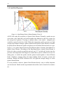
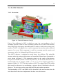
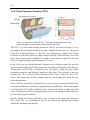
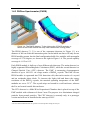
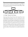
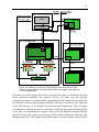
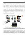
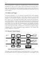

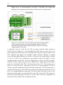
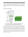
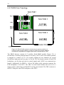
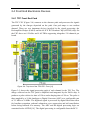
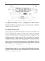
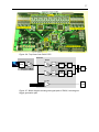
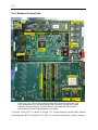
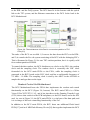
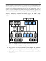
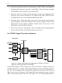
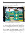


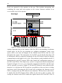
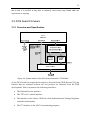
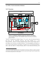
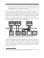
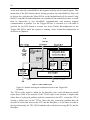
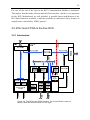
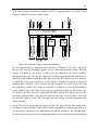
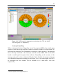
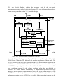
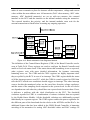
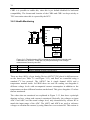
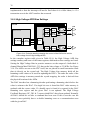
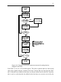

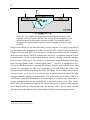
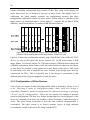
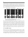
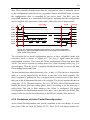
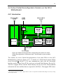
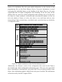
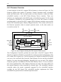
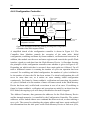
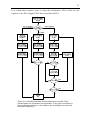
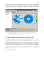

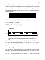
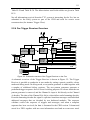
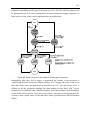
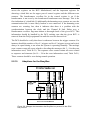
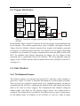
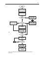
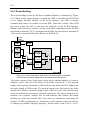
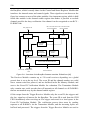

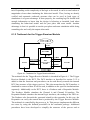
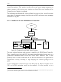

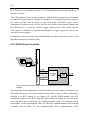
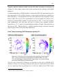
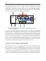


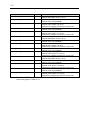
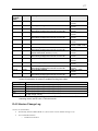
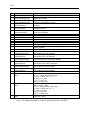
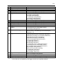
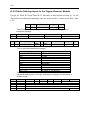
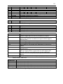
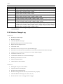
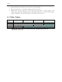
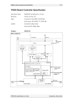


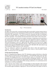
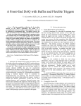

![Indico User Guide - Indico [Home]](http://vs1.manualzilla.com/store/data/006906671_1-144eb090a744237196a75cbdc9f1656c-150x150.png)