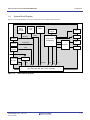
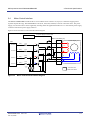
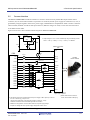
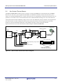
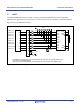
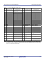
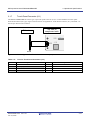
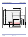
1
User’s Manual
HMI Expansion Board
32
R0K50564MB001BR
User's Manual
Renesas Microcomputer
RX64M Group
All information contained in these materials, including products and product specifications,
represents information on the product at the time of publication and is subject to change by
Renesas Electronics Corporation without notice. Please review the latest information published by
Renesas Electronics Corporation through various means, including the Renesas Electronics
Corporation website (http://www.renesas.com).
www.renesas.com
Rev.1.01
2015.1
Notice
1.
Descriptions of circuits, software and other related information in this document are provided only to illustrate the operation of
semiconductor products and application examples. You are fully responsible for the incorporation of these circuits, software,
and information in the design of your equipment. Renesas Electronics assumes no responsibility for any losses incurred by you
or third parties arising from the use of these circuits, software, or information.
2.
Renesas Electronics has used reasonable care in preparing the information included in this document, but Renesas Electronics
does not warrant that such information is error free. Renesas Electronics assumes no liability whatsoever for any damages
incurred by you resulting from errors in or omissions from the information included herein.
3.
Renesas Electronics does not assume any liability for infringement of patents, copyrights, or other intellectual property rights of
third parties by or arising from the use of Renesas Electronics products or technical information described in this document. No
license, express, implied or otherwise, is granted hereby under any patents, copyrights or other intellectual property rights of
Renesas Electronics or others.
4.
You should not alter, modify, copy, or otherwise misappropriate any Renesas Electronics product, whether in whole or in part.
Renesas Electronics assumes no responsibility for any losses incurred by you or third parties arising from such alteration,
modification, copy or otherwise misappropriation of Renesas Electronics product.
5.
Renesas Electronics products are classified according to the following two quality grades: “Standard” and “High Quality”. The
recommended applications for each Renesas Electronics product depends on the product’s quality grade, as indicated below.
“Standard”:
Computers; office equipment; communications equipment; test and measurement equipment; audio and visual
equipment; home electronic appliances; machine tools; personal electronic equipment; and industrial robots etc.
“High Quality”: Transportation equipment (automobiles, trains, ships, etc.); traffic control systems; anti-disaster systems; anticrime systems; and safety equipment etc.
Renesas Electronics products are neither intended nor authorized for use in products or systems that may pose a direct threat to
human life or bodily injury (artificial life support devices or systems, surgical implantations etc.), or may cause serious property
damages (nuclear reactor control systems, military equipment etc.). You must check the quality grade of each Renesas
Electronics product before using it in a particular application. You may not use any Renesas Electronics product for any
application for which it is not intended. Renesas Electronics shall not be in any way liable for any damages or losses incurred
by you or third parties arising from the use of any Renesas Electronics product for which the product is not intended by Renesas
Electronics.
6.
You should use the Renesas Electronics products described in this document within the range specified by Renesas Electronics,
especially with respect to the maximum rating, operating supply voltage range, movement power voltage range, heat radiation
characteristics, installation and other product characteristics. Renesas Electronics shall have no liability for malfunctions or
damages arising out of the use of Renesas Electronics products beyond such specified ranges.
7.
Although Renesas Electronics endeavors to improve the quality and reliability of its products, semiconductor products have
specific characteristics such as the occurrence of failure at a certain rate and malfunctions under certain use conditions. Further,
Renesas Electronics products are not subject to radiation resistance design. Please be sure to implement safety measures to
guard them against the possibility of physical injury, and injury or damage caused by fire in the event of the failure of a Renesas
Electronics product, such as safety design for hardware and software including but not limited to redundancy, fire control and
malfunction prevention, appropriate treatment for aging degradation or any other appropriate measures. Because the evaluation
of microcomputer software alone is very difficult, please evaluate the safety of the final products or systems manufactured by
you.
8.
Please contact a Renesas Electronics sales office for details as to environmental matters such as the environmental compatibility
of each Renesas Electronics product. Please use Renesas Electronics products in compliance with all applicable laws and
regulations that regulate the inclusion or use of controlled substances, including without limitation, the EU RoHS Directive.
Renesas Electronics assumes no liability for damages or losses occurring as a result of your noncompliance with applicable laws
and regulations.
9.
Renesas Electronics products and technology may not be used for or incorporated into any products or systems whose
manufacture, use, or sale is prohibited under any applicable domestic or foreign laws or regulations. You should not use
Renesas Electronics products or technology described in this document for any purpose relating to military applications or use
by the military, including but not limited to the development of weapons of mass destruction. When exporting the Renesas
Electronics products or technology described in this document, you should comply with the applicable export control laws and
regulations and follow the procedures required by such laws and regulations.
10. It is the responsibility of the buyer or distributor of Renesas Electronics products, who distributes, disposes of, or otherwise
places the product with a third party, to notify such third party in advance of the contents and conditions set forth in this
document, Renesas Electronics assumes no responsibility for any losses incurred by you or third parties as a result of
unauthorized use of Renesas Electronics products.
11. This document may not be reproduced or duplicated in any form, in whole or in part, without prior written consent of Renesas
Electronics.
12. Please contact a Renesas Electronics sales office if you have any questions regarding the information contained in this document
or Renesas Electronics products, or if you have any other inquiries.
(Note 1) “Renesas Electronics” as used in this document means Renesas Electronics Corporation and also includes its majorityowned subsidiaries.
(Note 2) “Renesas Electronics product(s)” means any product developed or manufactured by or for Renesas Electronics.
(2012.4)
WEEE Directive
Renesas development tools and products are directly covered by the European Union's Waste
Electrical and Electronic Equipment, (WEEE), Directive 2002/96/EC.
As a result, this equipment, including all accessories, must not be disposed of as household
waste but through your locally recognised recycling or disposal schemes.
As part of our commitment to environmental responsibility Renesas also offers to take back the
equipment and has implemented a Tools Product Recycling Program for customers in Europe.
This allows you to return equipment to Renesas for disposal through our approved Producer
Compliance Scheme.
To register for the program, click here "http://www.renesas.com/weee".
About This Manual
1. Purpose and Target Readers
This manual is designed to provide the user with an understanding of the functions and operating specifications of this
extension board. A basic knowledge of electrical circuits, logical circuits, and microcomputers (MCUs) is necessary in
order to use this manual.
This manual is composed of an overview of the expansion board; its functional and operational specifications.
Carefully read all notes described in the body of text in the manual.
The Revision History summarizes the modifications and additions to the previous versions. Refer to the text of the manual
for details.
The following document applies to the RX64M HMI Expansion Board R0K50564MB001BR.
Document Type
User's Manual
Description
Document Title
Describes functional specifications
HMI Expansion Board
(devices, memory maps, electrical
R0K50564MB001BR
characteristics), and operational
User's Manual
Document No.
This publication
specifications (connectors, and
switches)
The following documents apply to the RX64M group. Make sure to refer to the latest version of these documents which
can be obtained from Renesas Electronics website.
Document Type
User's Manual: Hardware
Description
Document Title
Hardware specifications (pin
RX64M Group User’s
assignments, memory maps,
manual: Hardware
Document No.
R01UH0377EJ
peripheral function specifications,
electrical characteristics, timing
charts) and operation description
Application note
Applications, sample programs, etc.
RENESAS TECHNICAL
Information regarding product
UPDATE
specifications, documents, etc.
Available on Renesas Electronics website
2. Frequently Used Abbreviations and Acronyms
ACIA
Asynchronous Communication Interface Adapter
bps
Bits per second
CRC
Cyclic Redundancy Check
DMA
Direct Memory Access
DMAC
Direct Memory Access Controller
GSM
Global System for Mobile Communications
Hi-Z
High Impedance
IEBus
Inter Equipment bus
I/O
Input/Output
IrDA
Infrared Data Association
LSB
Least Significant Bit
MSB
Most Significant Bit
NC
Non-Connection
PLL
Phase Locked Loop
PWM
Pulse Width Modulation
SFR
Special Function Registers
SIM
Subscriber Identity Module
UART
Universal Asynchronous Receiver/Transmitter
VCO
Voltage Controlled Oscillator
All trademarks and registered trademarks are the property of their respective owners.
Table of Contents
1.
2.
3.
Overview.................................................................................................................................................... 1-1
1.1
Overview ......................................................................................................................................................... 1-1
1.2
System Configuration ...................................................................................................................................... 1-2
1.3
External Specifications .................................................................................................................................... 1-3
1.4
System Block Diagram .................................................................................................................................... 1-4
1.5
Absolute Maximum Ratings ............................................................................................................................ 1-5
1.6
Operating Conditions....................................................................................................................................... 1-5
Functional Specifications........................................................................................................................... 2-1
2.1
Function Overview .......................................................................................................................................... 2-1
2.2
Sound I/O Interface.......................................................................................................................................... 2-2
2.3
7-Segment LEDs and User LEDs .................................................................................................................... 2-3
2.4
Motor Control Interface ................................................................................................................................... 2-4
2.5
Camera Interface.............................................................................................................................................. 2-5
2.6
Non-Contact Thermal Sensor .......................................................................................................................... 2-6
2.7
eMMC.............................................................................................................................................................. 2-7
2.8
Touch Panel Interface ...................................................................................................................................... 2-8
2.9
USB Battery Charge Controller ....................................................................................................................... 2-9
2.10
Power Supply Wiring..................................................................................................................................... 2-10
Operational Specifications......................................................................................................................... 3-1
3.1
Connector Overview ........................................................................................................................................ 3-1
3.1.1
RSK+ for RX64M CPU Board Connectors (JA1 to JA3, JA5, JA6, SSI, and PDC).............................. 3-2
3.1.2
Sound I/O Connectors (J1, J2, J3, and J4) .............................................................................................. 3-7
3.1.3
Motor Connector (J7).............................................................................................................................. 3-9
3.1.4
External Power Supply Connector (J8)................................................................................................... 3-9
3.1.5
Camera Connector (J9) ......................................................................................................................... 3-10
3.1.6
Sensor Connector (J10)......................................................................................................................... 3-11
3.1.7
Touch Panel Connector (J11)................................................................................................................ 3-12
3.1.8
GND Connector (J12)........................................................................................................................... 3-13
3.2
Operation Parts Layout .................................................................................................................................. 3-14
3.2.1
Jumpers (JP1, JP4 to JP8) ..................................................................................................................... 3-15
3.2.2
LEDs..................................................................................................................................................... 3-18
3.2.3
Potentiometer........................................................................................................................................ 3-18
3.2.4
Test Pins ............................................................................................................................................... 3-19
3.3
Settings for RSK+ for RX64M CPU Board................................................................................................... 3-20
3.4
Dimensions .................................................................................................................................................... 3-24
Appendix R0K50564MB001BR Schematics.........................................................................................................1
HMI expansion board R0K50564MB001BR
1.
Overview
1.1
Overview
1. Overview
The HMI expansion board R0K50564MB001BR is a functional expansion board used by connecting with the RSK+ for
RX64M CPU Board. The features of the HMI expansion board are listed below.
• Pin jacks for sound input dual system (mic/ line-in) and sound output dual system (headphone/line-out) are included.
Asahi Kasei AK4642EN is included as Audio Codec LSI to make it possible to input/output high quality sound data.
The sound data can also be input to the RX64M ADC.
• 7-segment LEDs (for 10 digits) is included, which can be used to display characters for demonstrations.
• Stepping motor control circuit and connectors for motor connection are included, which enable motor operation
working with the RSK+ for RX64M CPU Board communication systems and display.
• Connectors for camera connection are included. These connectors can be used as input devices for the camera with
the PDC interface.
• Connectors for OMRON Non-Contact Thermal Sensor D6T-44L-06 are included as a human sensor. These
connectors can be sued in demonstrations.
• An eMMC device with 8GB is included.
• A touch panel connector (8-pin FFC) for R8C/3JT touch panel demonstration board (R0K521336C0001BR) is
included.
• A USB battery charge controller with RX64M USB Full-Speed (USBA) is included, which makes it possible to evaluate
the lithium-ion battery charging function from VBUS (with R2A20057BX) and the power supply function from
lithium-ion battery to VBUS.
R20UT3056EJ0101 Rev.1.01
Jan. 16, 2015
1-1
HMI expansion board R0K50564MB001BR
1.2
1. Overview
System Configuration
Figure 1.1 shows the Example of System Configuration with HMI expansion board.
RSK+ for RX64M CPU board
MCU
Lithium-ion
JA6
JA5
JA2
JA1
battery
JA3
SSI
AC adapter for
RSK+ for RX64M
CPU board
PDC
HMI expansion board
R0K50564MB001BR
JA6
JA5
JA2
JA1
Sound I/O
L_OUT
R_OUT
L_IN
R_IN
JA3
Audio
Codec
AK4642EN
HP
Motor power supply
Motor
Power
MIC
J25(SSI)
J24(PDC)
TouchPanel
FFC
7-segment LED (10 digits)
Motor
Connector
Sensor
Camera
Stepping motor
(2-phase unipolar driving)
Touch panel
to R8C/3JT
demonstration board
Figure 1.1
Human
sensor
PDC camera
Example of System Configuration
R20UT3056EJ0101 Rev.1.01
Jan. 16, 2015
1-2
HMI expansion board R0K50564MB001BR
1.3
1. Overview
External Specifications
Table 1.1 lists the External Specifications for the HMI expansion board.
Table 1.1
External Specifications
No.
1
Item
Sound I/O interface
Description
Includes a sound I/O interface with RX64M SSI
• Includes Asahi Kasei AK4642EN as Audio Codec LSI
-
Input clock : 12.288MHz
-
Sampling rate : 48kHz/24kHz/16kHz/12kHz are supported
• Supports dual systems for 16-bit stereo Input/output
-
Microphone, headphone (stereo mini-jack) : 1 for each
-
Line-in, line-out (RCA jack×2) : 1 set for each
• Sound input data can be input to RX64M ADC (Selected by JP8)
2
LEDs
Includes 7-segment LEDs and individual LEDs
• Includes 7-segment LEDs for 10 digits, which can be used to display
characters
• 4 user LEDs, LEDs for motor external power supply and charger IC/STAT
3
Motor control interface
Includes a stepping motor (2-phase unipolar driving) control interface
• Includes a 6-pin connector for motor driver circuit and motor connection
• Motor power supply connector is prepared, which can be switched by using
the RSK power supply and jumper
4
Camera interface
Includes a camera interface which can be connected to PDC for image input
• Includes 2.7 system power supply generator, a level shifter circuit, and a
16-pin DIP connector expecting that OmniVision OV7670 camera module
is connected.
5
Non-contact thermal sensor
6
eMMC
Includes OMRON Non-Contact Thermal Sensor D6T-44L-06 to be connected
on I2C as a human sensor
Includes the 8GB eMMC that controlled by RX64M MMCHI for
Backward-compatible mode access.
Note that this should be controlled exclusively from the SD card slot on RSK+
for RX64M CPU Board.
7
Touch panel interface
Includes a connector (8-pin FFC) for R8C/3JT touch panel demonstration
board (R0K521336C0001BR)
8
USB battery charge
Includes a USB battery charge controller with RX64M USB Full-Speed(USBA)
controller
• Test pin (3-pin) is prepared to connect the lithium-ion battery
• Lithium-ion battery charging function from VBUS (with R2A20057BX)
• Power supply function from lithium-ion battery to VBUS
9
RSK interface
10
Board specifications
Includes the following connectors for RSK+ for RX64M CPU Board
JA1/JA2(26-pin), JA3(50-pin), JA5/JA6(24-pin), PDC(20-pin), and SSI(12-pin)
• Dimensions: 180 mm×180 mm
• Mounting form: 4-layer, double-sided (Thickness: 1.6mm)
• Number of board: 1
R20UT3056EJ0101 Rev.1.01
Jan. 16, 2015
1-3
HMI expansion board R0K50564MB001BR
1.4
1. Overview
System Block Diagram
Figure 1.2 shows the Example of System Configuration for the HMI expansion board.
USB
battery
charge
controller
7-seg
LED
eMMC
Oscillator
HP
12.288MHz
PORT
LINE OUT
SCI(I2C)
Sensor
connector
Audio Codec
(AK4642EN)
Touch panel
connector
SCI(UART)
Camera
connector
PDC
MIC
Switches
LINE IN
5V
Jumper
Connectors
for motor
5V
MMCHI
SSI
SCI
ADC
(I2C)
PORT
Through-hole for expansion connectors
(JA1,JA2,JA3,JA5,JA6, PDC, and SSI)
Figure 1.2
System Block Diagram
R20UT3056EJ0101 Rev.1.01
Jan. 16, 2015
1-4
HMI expansion board R0K50564MB001BR
1.5
1. Overview
Absolute Maximum Ratings
Table 1.2 lists the Absolute Maximum Ratings for the HMI expansion board.
Table 1.2
Absolute Maximum Ratings
Symbol
Item
Rated Value
Remarks
5VCC
5V system power supply voltage
-0.5V to 6.0V
Vss reference
3VCC
3.3V system power supply voltage
-0.5V to 4.1V
Vss reference (Only for direct supply)
Topr
Operating ambient temperature*
0°C to 50°C
Do not expose to condensation or corrosive
Tstg
Storage ambient temperature*
-20°C to 60°C
gases.
Do not expose to condensation or corrosive
gases.
[Note] * The ambient temperature is the air temperature immediate to the board.
1.6
Operating Conditions
Table 1.3 shows the Operating Conditions for the HMI expansion board.
Table 1.3
Operating Conditions
Symbol
5VCC
Item
5V system power supply voltage
Rated Value
4.75V to 5.25V
Remarks
The value is defined on the CPU board
(Vss reference)
3VCC
3.3V system power supply voltage
3.0V to 3.6V
The value is defined on the CPU board
(Vss reference)
-
Board maximum consumption
Up to 1.5A
current
Topr
Operating ambient temperature*
0°C to 50°C
Do not expose to condensation or corrosive
gases.
[Note] * The ambient temperature is the air temperature immediate to the board.
R20UT3056EJ0101 Rev.1.01
Jan. 16, 2015
1-5
HMI expansion board R0K50564MB001BR
R20UT3056EJ0101 Rev.1.01
Jan. 16, 2015
1. Overview
1-6
HMI expansion board R0K50564MB001BR
2.
Functional Specifications
2.1
Function Overview
2.Functional Specifications
Table 2.1 lists the R0K50564MB001BR Function Modules.
Table 2.1 R0K50564MB001BR Function Modules
Section
2.2
Function
Sound I/O Interface
Description
Includes a sound I/O interface with dual system
• Asahi Kasei AK4642EN is used as AudioCodec LSI
• A 12.288MHz oscillator is included as a master clock
48kHz/24kHz/16kHz/12kHz are supported for sampling rate
• Stereo mini jacks for mic input and headphone output
• Stereo RCA jacks for line-in input and line-out output
• Mic and line-in can be input to RX64M ADC2 and ADC3 (JP8 is used)
User LEDs
• 7-segment LEDs (Red): 10 (Can be used to display characters)
• User LEDs: 4
2.4
Motor Control Interface
Includes a driver circuit and connectors for stepping motor (2-phase unipolar
2.5
Camera Interface
Includes a camera interface which can be connected to PDC for image input
2.3
7-Segment LEDs and
driving)
• OmniVision OV7670 camera module can be connected
• 2.7 system power supply generator for camera module and level shifter circuit
• A 16-pin DIP connector
2.6
Non-Contact Thermal
Includes a non-contact thermal sensor interface as a human sensor
Sensor
• Omron D6T-44L-06 can be connected
• I2C interface level shifter circuit
2.7
eMMC
Includes an eMMC device with 8GB
2.8
Touch Panel Interface
Includes a 8-pin FFC connector for R8C/3JT touch panel demonstration board
2.9
USB Battery Charge
Includes a USB battery charging function with RX64M USB Full-Speed (USBA)
ControllerUSB Battery
Charge Controller
• Lithium-ion battery charging function from VBUS (with R2A20057BX)
• Power supply function from lithium-ion battery to VBUS
Power Supply Wiring
3.3V and 5V system power supply and ground wiring from JA1,JA2 and JA6
(R0K521336C0001BR)
2.10
connector
-
Operational Specifications Chapter 3 describes details of connectors, jumpers, and LEDs.
R20UT3056EJ0101 Rev.1.01
Jan. 16, 2015
2-1
HMI expansion board R0K50564MB001BR
2.2
2.Functional Specifications
Sound I/O Interface
The R0K50564MB001BR includes Asahi Kasei Audio Codec LSI AK4642EN to support the sound I/O function. The
RX64M SCIg Ch2 is used to control the Audio Codec LSI in simple I2C mode, and the SSI is used to transfer the sound
data. The port P51 is used to control power-down mode, and the port PB7 is used for BEEP input. The potentiometer
(VR1) is also included in the R0K50564MB001BR for BEEP sound control.
On the R0K50564MB001BR, the sound data can be input to the RX64M ADC by setting JP8 because ADC2 and ADC3
used for sound data input are also connected to the USB battery charge controller.
Figure 2.1 shows the Sound I/O Interface Block Diagram.
JA1
11 ADC2
12 ADC3
AVCC
Audio Codec LSI
(AK4642EN)
3VCC
2.2uF
15
4
21
3VCC
JA6
SSCL2
SSDA2
1.5kΩ
×2
6
9
9
10
JA3
PB7
AVDD
MPWR
2
1
1
2
31
3
4
32
5
6
7
8
9
10
30
11
12
29
13
14
15
16
R2
17
18
R1
19
20
HVDD
I2C
RIN1
SCL
SDA
R62 47kΩ Optional
8
LIN2
CAD0
RIN2
R61 47kΩ
VSS
47
VCOM
LIN1
12
3VCC
P51
DVDD
7
PDN
16
47kΩ
VSS
28
VR1
1uF
2.2kΩ×2
MIC IN (J1)
3
1
2
1uF×2
LINE IN (J3)
L2
L1
1uF×2
BTT_MON
JP8
MIN
0.1uF
BTT_TEMP
20kΩ
To USB battery
charge controller
AVSS
SSI
LINE OUT (J4)
SSIRXD0
SSITXD0
SSISCK0
SSIWS0
AUDIOCLK
10
12
12
11
9
14
11
13
5
18
3
17
2
10kΩ
1
5
25
JP1
4700pF
SDTO
LOUT
SDTI
ROUT
L2
27
26
1uF×2
BICK
R1
AVSS
MCKO
HP OUT (J2)
MCKI
VCOC
MUTET
HPL
HPR
3
24
1
23
47uF×2
Oscillator
22
(12.288MHz)
16
R2
20kΩ×2
LRCK
1uF
3
L1
220Ω×2
2
6.8Ω×2
0.22uF×2
AVSS
HVSS
SPP
DVSS
SPN
20
AVSS
10Ω×2
19
AVSS
3VCC
L1
AVSS
L2
0.1uF
10uF
BLM21PG300SN1
VSS
VSS
AVCC
AVSS
• JP8 setting for sound I/O
Set jumpers Short/Open using AK4642EN: Short JP8_3-4, 7-8, 11-12, and 15-16, Open others
Set jumpers for MIC IN using ADC of RX64M: Short JP8_1-2, 5-6, 11-12, and 15-16, Open others
Set jumpers for LINE IN using ADC of RX64M: Short JP8_3-4, 7-8, 9-10, and 13-14, Open others
• JP8 setting for ADC of RX64M
Set jumpers for MIC IN using ADC of RX64M: Short JP8_1-2 and 5-6, Open JP8_3-4, 7-8, 9-10, 13-14, 17-18, and 19-20
Set jumpers for LINE IN using ADC of RX64M: Short JP8_9-10 and 13-14, Open JP8_1-2, 5-6, 11-12, 15-16, 17-18, and 19-20
Set jumpers for USB battery charge controller using ADC of RX 64M: Short JP8_17-18 and 19-20, Open JP8_1-2, 5-6, 9-10, and 13-14
* Pull-up/down on JA connector signals are not included .
Figure 2.1
Sound I/O Interface Block Diagram
R20UT3056EJ0101 Rev.1.01
Jan. 16, 2015
2-2
HMI expansion board R0K50564MB001BR
2.3
2.Functional Specifications
7-Segment LEDs and User LEDs
The R0K50564MB001BR includes ten 7-segment LEDs with a total of 18 general ports from the application header JA3
and four user LEDs with general ports from JA2 and JA6.
Figure2.2 shows the Block Diagram for 7-Segment LEDs and User LEDs.
47kΩ
3VCC
47kΩ
7-segment LED
(1st digit)
2.2kΩ
3VCC
7-segment LED
(6th digit)
2.2kΩ
COM
COM
A
A
B
B
C
C
D
D
E
E
F
F
G
G
DP
47kΩ
3VCC
User LED0
P91
10
LED0
1kΩ
Green
User LED1
P93
12
LED1
1kΩ
47kΩ
JA6
User LED2
P10
LED2
LED3
COM
COM
A
A
B
B
C
C
D
D
E
E
F
F
G
G
DP
47kΩ
7-segment LED
(3rd digit)
2.2kΩ
3VCC
7-segment LED
(8th digit)
2.2kΩ
1kΩ
User LED3
15
7-segment LED
(7th digit)
2.2kΩ
3VCC
Green
P11
3VCC
DP
Green
16
47kΩ
7-segment LED
(2nd digit)
2.2kΩ
JA2
DP
3VCC
1kΩ
Green
COM
COM
A
A
B
B
C
C
D
D
E
E
F
F
G
G
DP
47kΩ
DP
3VCC
47kΩ
7-segment LED
(4th digit)
2.2kΩ
3VCC
7-segment LED
(9th digit)
2.2kΩ
COM
COM
A
A
B
B
C
C
D
D
E
E
F
F
G
G
DP
47kΩ
2.2kΩ
JA3
P61
P62
P63
P64
P65
PA3
PA4
PA5
PA6
PA7
28
7SEG_com1
50
7SEG_com2
49
7SEG_com3
26
7SEG_com4
46
7SEG_com5
4
7SEG_com6
5
7SEG_com7
6
7SEG_com8
7
7SEG_com9
8
7SEG_com10
9
7SEG_a
10
7SEG_b
11
7SEG_c
12
7SEG_d
13
7SEG_e
14
7SEG_f
15
7SEG_g
44
7SEG_DP
DP
3VCC
7-segment LED
(5th digit)
47kΩ
2.2kΩ
3VCC
7-segment LED
(10th digit)
COM
COM
A
A
B
B
C
C
D
D
E
E
F
F
G
G
DP
DP
3VCC
PB0
PB1
PB2
PB3
PB4
PB5
PB6
P53
74LV541
OE1 OE2 GND
330Ω×8
VSS
Figure2.2
Block Diagram for 7-Segment LEDs and User LEDs
R20UT3056EJ0101 Rev.1.01
Jan. 16, 2015
2-3
HMI expansion board R0K50564MB001BR
2.4
2.Functional Specifications
Motor Control Interface
The R0K50564MB001BR includes the drive circuit and the motor connector J7 (6-pin) to control the stepping motor
(2-phase unipolar driving). The RX64M MTU3 Ch7 (PA1, PA2, P66, and P67) is used to control the motor. The power
supply (5V) for motor drive can be supplied by selecting either the application header JA1-1 or the external power supply
connector J8 at JP4 for power supply selection.
Figure2.3 shows the Motor Control Interface Block Diagram.
5V power supply for motor drive
Power block
Motor connector (J7)
JA5
MTIOC7A
MTIOC7B
MTIOC7C
MTIOC7D
21
MTR_A
23
MTR_B
22
MTR_C
24
MTR_D
2.2kΩ
2.2kΩ
2.2kΩ
2.2kΩ
1
A
2
+DC
3
A
4
B
5
+DC
6
B
2-phase stepping motor
A
B
A
B
4.7kΩ
×4
: Connected to the
outside of the board
VSS
Figure2.3
Motor Control Interface Block Diagram
R20UT3056EJ0101 Rev.1.01
Jan. 16, 2015
2-4
HMI expansion board R0K50564MB001BR
2.5
2.Functional Specifications
Camera Interface
The R0K50564MB001BR includes the interface to connect a camera for 8-bit parallel data output and the camera
connector (J9). OV7670 camera module is expected to be connected, and the power supply for camera drive (2.75V) is
generated by using the regulator from 5VCC power supply. RX64M SCI6 in simplified I2C mode is used to control the
camera module, and PDC is used for data input. However, different voltages are used, so a bus switch is inserted as a
level shifter between them.
Figure2.4 shows the Camera Interface Block Diagram on R0K50564MB001BR.
5VCC
LT1117
VIN
2_7VCC
VOUT
• Output voltage of LT1117 can be calculated by using the following formula .
ADJ
VOUT = 1.25V ( 1 + R2/R1 ) = 1.25 ( 1 + 147/121 ) = 2.768595V
121Ω
10uF
10uF
100uF
147Ω
Camera connector
(J9)
1
VSS
PDC
SCL
SDA
1.5kΩ
×2
0Ω×12
20
3
4
19
VCC
SIO_C
OV7670
camera module
SIO_O
2_7VCC
PCKO
5
3VCC
VSYNC
HSYNC
PIXCLK
8
74CB3T1G125
EN
XCLK
3VCC
VSS
9
5
74CB3T3125
10
6
8
7
EN
VSYNC
HREF
PCLK
3VCC
PIXD7
PIXD6
PIXD5
PIXD4
PIXD3
PIXD2
PIXD1
PIXD0
VSS
11
9
74CB3T3245
12
10
13
11
14
12
15
13
16
14
17
15
18
16
EN
33Ω×12
R×11
(DNF)
VSS
2
VSS
• The following process are required because the power supply on MCU
(3VCC) is 3.3V and
D7
D6
D5
D4
D3
D2
D1
D0
GND
2.54mm pitch 16Pin×2
Right-angle receptacle
(Samtec SSW-108-02-G-D-RA, or
Hirose HIF3H-16DB-2.54DS(71))
the one on camera (2_7VCC) is 2.75V.
- I2C pull-up is performed by using the power supply on camera (2_7VCC).
- 74CB3Txx is inserted to the PDC-related signal as a level shifter.
* 74CB3Txx is recognized as 'H' when VIN is about 60% of power supply voltage.
It outputs Vo voltage with 90% of power supply voltage when IOH is 16mA.
Figure2.4
Camera Interface Block Diagram
R20UT3056EJ0101 Rev.1.01
Jan. 16, 2015
2-5
HMI expansion board R0K50564MB001BR
2.6
2.Functional Specifications
Non-Contact Thermal Sensor
The R0K50564MB001BR includes the sensor connector to connect the MEMS non-contact thermal sensor (OMRON
D6T-44L-06). The 5VCC power supplied from the RSK+ for RX64M CPU Board is used for the sensor drive power
supply (5V), and the RX64M SCIg Ch7 is used to control the sensor in simplified I2C mode. Because this sensor uses 5V
operation, a level shifter circuit is inserted between the sensor and the RX64M. The SCIg Ch7 is also connected to the
touch panel interface and the USB battery charge control circuit. The USB battery charge controller can be applied at the
same time because it is used in simple I2C mode, but the touch panel interface cannot be applied at the same time
because it is used in UART mode. Either JP5 or JP6 should be selected to use the touch panel interface.
Figure2.5 shows the Non-Contact Thermal Sensor Block Diagram on R0K50564MB001BR.
D6T-44L-06
JA2
A-RXD7
A-TXD7
3VCC
5VCC
VCCA
VCCB
SDAA
SDAB
SCLA
SCLB
Sensor connector
(J10)
JP5
8
1
6
1
2
2
3
1.5kΩ
×2
3
JP6
1.5kΩ
×2
4
3
1
EN
PCA9517
2
VSS
VSS
VCC
SCL
SDA
Sensorspecific cable
GND
SM05B-GHS-TB(JST)
Sensor-specific cable
SDA7
SCL7
To USB battery charge controller
A-TXD7
A-RXD7
To touch panel interface
Housing: GHR-04V-2(JST)
Contact: SSHL-002T-P0.2(JST)
Figure2.5
Non-Contact Thermal Sensor Block Diagram
R20UT3056EJ0101 Rev.1.01
Jan. 16, 2015
2-6
HMI expansion board R0K50564MB001BR
2.7
2.Functional Specifications
eMMC
The R0K50564MB001BR includes one eMMC controlled by the RX64M MMCHI. Please note that the RX64M
MMCHI control signals cannot be used with the SD card slot and the external bus on the RSK+ for RX64M CPU Board
at the same time because it is multiplexed with the SDHI control signals and the external bus signals.
Figure2.6 shows the eMMC Block Diagram.
3VCC
100kΩ×9
Bus switch circuit
JA3
(MMC_D7-B)
D11
18
(MMC_D6-B)
D10
17
J5
(MMC_D5-B)
D9 16
J4
(MMC_D4-B)
D8 15
J3
(MMC_D3-B)
D3 10
J2
(MMC_D2-B)
D2 9
H5
(MMC_D1-B)
D7 14
H4
(MMC_D0-B)
D6 13
H3
(MMC_CLK-B)
D5 12
W6
(MMC_CMD-B)
D4 11
W5
(MMC_RESn-B)
D15
22
(MMC_CD-B)
D14
21
eMMC
4.7kΩ
22Ω×11
J6
U5
3VCC
DAT7
VCC
DAT6
VCCQ
DAT5
VDDI
DAT4
1uF
DAT2
DAT1
DAT0
CLK
CMD
RESn
VSS
VSSQ
100kΩ
Optional
3VCC
100kΩ
0.1uF
DAT3
VSS
VSS
100kΩ
EN
JP7
VSS
* The eMMC signals should pass through the bus switch circuit controlled by JP7 to enable all signals to be
concurrently connected/disconnected.
(This bus switch uses SH74CB3Q3245 and SH74CB3Q3125, and short JP6 when the eMMC is used.)
Figure2.6
eMMC Block Diagram
R20UT3056EJ0101 Rev.1.01
Jan. 16, 2015
2-7
HMI expansion board R0K50564MB001BR
2.8
2.Functional Specifications
Touch Panel Interface
The R0K50564MB001BR includes the 8-pin FFC type connector (J11) to connect the R8C/3JT touch panel
demonstration board (TV type). The RX64M AD0 is used for analog input from the touch panel, and the RX64M SCIg
Ch7 is used to communicate with the R8C/3JT in UART mode. The SCIg Ch7 is also connected to the non-contact
thermal sensor and the USB battery charge control circuit, so the 8-pin FFC type connector (J11) cannot be used with
these devices at the same time.
Figure2.7 shows the Touch Panel Interface Block Diagram.
3VCC
JA2
Touch panel connector
(J11)
1
RESET
1
0Ω
2
3
4
JA1
5
AN0
9
0Ω
6
7
8
From Non-contact
thermal sensor
block
A-RXD7
A-TXD7
VSS
VCC
RESET
MODE
TXD
RXD
DAOUT
FFC-specific
cable
NC
GND
52207-0817
To touch panel
R8C/3JT demonstration board
Figure2.7
Touch Panel Interface Block Diagram
R20UT3056EJ0101 Rev.1.01
Jan. 16, 2015
2-8
HMI expansion board R0K50564MB001BR
2.9
2.Functional Specifications
USB Battery Charge Controller
The R0K50564MB001BR supports the battery charging function and the power supply function to VBUS using the
RX64M USB Full-Speed (USBA) which corresponds to the Battery Charging Class. The USB Full-Speed ports on the
RSK+ for RX64M CPU Board are used to evaluate the lithium-ion battery charging function from VBUS and the VBUS
power supply function from the lithium-ion battery by using the VBUS signal from the USB Hi-Speed ports via the
application header JA6. The battery charger IC includes the R2A20057BX, and the RX64M SCIg Ch7 is used in
simplified I2C mode to control the charger IC. The SCIg Ch7 is also connected to the non-contact thermal sensor and the
touch panel interface, but the latter cannot be used at the same time because it is used in UART mode. ADC2 and ADC3
are used to monitor the battery status and also to input the sound data. The JP8 is used to select either for monitoring
battery status or inputting sound data.
Figure2.8 the USB Battery Charge Controller Block Diagram.
JA6
EXT_VBUS
EXT_BATT
17
L7
19
L8
L3
EXT_CHG
21
L9
LTC3428
4.7uF
Ferrite beads×3
8
4
10kΩ
5
22pF
7
1
11
1000pF
VIN
VOUT
SHDNn
SWA
Vc
SWB
AGND
FB
PGNDA
L4
2.2uH
PGNDB
2.2uH
3
2
Dxx
9
Dyy
383kΩ
22uF
121kΩ
6
10
TGND
JA3
A21(PC5)
A0(PA0)
42
1
0Ω×2
VSS
SHDNn
USUP
* Each capacity (condenser)
is allocated nearby IC.
750Ω
A2
A3
VSS
LED4
B3
D1
E1
TP1
C4
From non-contact
thermal sensor
block
L5
R2A20057BX
0.1uF 6.8uF
SCL7
E4
SDA7
E3
18kΩ×2 D2
E2
C1
B2
IN1
DOUT1
IN2
DOUT2
IN3
SYS1
STATn
SYS2
POKn
SGn
USUP
FBC
SCL
SDA
BAT1
BAT2
DP
THVDD
DM
SGREF
GND
DDGND
TH
CTL
CENn
2.2uH
HAT1069C
A1
B1
0.1uF
22uF
A4
B4
TP2
D4
VSS
HAT1069C
C5
A5
B5
100kΩ
D5
51kΩ
D3
E5
C3
100kΩ
0.1uF
0Ω
C2
0Ω×2
VSS
From sound I/O
interface
(Optional)
VSS
BTT_TEMP
-
T
+
-
T
+
2.2uF 0.1uF
BTT_MON
VSS
5V system power supply line such as VBUS
4.xxV power supply line connected to the battery
Lithium-ion battery
GND
(Connected to the
outside of the board)
Figure2.8
USB Battery Charge Controller Block Diagram
R20UT3056EJ0101 Rev.1.01
Jan. 16, 2015
2-9
HMI expansion board R0K50564MB001BR
2.10
2.Functional Specifications
Power Supply Wiring
3.3V and 5V are supplied from the RSK+ for RX64M CPU Board via JA1,JA2 and JA3 connector. The 3.3V power is
supplied to all the interfaces and devices except the motor control interface, and the 5V power is supplied to the motor
control interface, the non-contact thermal sensor, and the camera interface. The power supplied to the camera interface is
used to generate 2.75V power supply for camera module driver. In the motor control interface, either the 5V power
supplied from JA1 connector or 5V input from the external power supply connector J8 is selected at JP4 to be used as 5V
power supply for motor drive.
Figure2.9 shows the Power Supply Wiring on R0K50564MB001BR.
External power supply
connector (J8)
External power supply LED
(LED5)
(DC5V supply)
JP4
1kΩ
2
Motor control
interface
3
JA1
Blue
1
5VCC
5V
1
Non-contact thermal
sensor
3VCC
3V3
GND
GND
3
2
4
Camera interface
JA2
GND
4
Sound I/O interface
JA6
GND
7-segment LEDs,
User LEDs
24
eMMC
Touch panel
interface
VSS
External 5V system power supply from 5VCC or Jxx
3VCC (3.3V system power supply)
GND
Figure2.9
Power Supply Wiring
R20UT3056EJ0101 Rev.1.01
Jan. 16, 2015
2-10
HMI expansion board R0K50564MB001BR
3.
Operational Specifications
3.1
Connector Overview
3. Operational Specifications
Figure 3.1 shows the R0K50564MB001BR Connector Assignments.
JA6
JA5
JA2
JA1
L_OUT
J4
R_OUT
L_IN
J3
R_IN
JA3
J2
HP
J8
J1
Mic
Motor
Power
TP_FFC
SSI
PDC
J7
Motor
Connector
J11
J10
Sensor
J9
Camera
:Connectors for RSK+ for RX64M CPU board
Figure 3.1
J12
:Other connectors
R0K50564MB001BR Connector Assignments
R20UT3056EJ0101 Rev.1.01
Jan. 16, 2015
3-1
HMI expansion board R0K50564MB001BR
3.1.1
3. Operational Specifications
RSK+ for RX64M CPU Board Connectors (JA1 to JA3, JA5, JA6, SSI, and PDC)
The R0K50564MB001BR has RSK connectors of the application headers (JA1 to JA3, JA5, and JA6) and connectors of
SSI, and PDC. These connectors can be used by connecting with the RSK+ for RX64M CPU Board.
Figure 3.2 shows the Pin Assignments for RSK Connectors (JA1 to JA3, JA5, JA6, SSI, and PDC). Table 3.1 to Table
3.7 list the pin names for RSK Connectors (JA1 to JA3, JA5, JA6, SSI, and PDC).
Top view of component side
24
23
JA6
JA6
L_OUT
2
J4
R_OUT
JA5
1
26
23
JA5
2
25
JA2
L_IN
24
1
26
JA2
JA1
25
JA1
J3
R_IN
2 1
2 1
2
1
J2
HP
JA3
50
49
JA3
J8
J1
Mic
TP_FFC
2
1
J11
SSI
PDC
PDC
11 1
20
19
J7
Motor
Connector
J10
Sensor
Figure 3.2
12 2
SSI
Motor
Power
J9
Camera
J12
Pin Assignments for RSK Connectors (JA1 to JA3, JA5, JA6, SSI, and PDC)
R20UT3056EJ0101 Rev.1.01
Jan. 16, 2015
3-2
HMI expansion board R0K50564MB001BR
Table 3.1
Pin
No.
3. Operational Specifications
Pins for Application Header (JA1)
Signal Name (Port)
Usage/Destination
Pin
No.
Signal Name (Port)
Usage/Destination
1
5V
5VCC
2
GND
GND
3
3V3
3VCC
4
GND
GND
5
AVCC
-
6
AVSS
-
7
AVREF
-
8
ADTRG
-
9
ADC0 (P40)
AD input for touch panel
10
ADC1
-
11
ADC2 (P42)
Sound I/O (L) or USB
12
ADC3 (P43)
Sound I/O (R) or USB
battery charge control
battery charge control
thermal monitor
voltage monitor
13
DA0
-
14
DA1
-
15
IO_0
-
16
IO_1
-
17
IO_2
-
18
IO_3
-
19
IO_4
-
20
IO_5
-
21
IO_6
-
22
IO_7
-
23
IRQ3/IRQAEC/M2_
-
24
IIC_EX
-
-
26
IIC_SCL
-
HSIN0
25
IIC_SDA
[Note] "-" in Usage/Destination column means that the pins are not used.
Table 3.2
Pin
No.
Pins for Application Header (JA2)
Signal Name (Port)
Usage/Destination
Pin
No.
Signal Name (Port)
1
RESET
Device reset
2
EXTAL
3
NMI
-
4
Vss1
5
WDT_OVF
-
6
Usage/Destination
GND via 0Ω resister
*1
SCIaTX (P90)
Non-contact thermal sensor,
USB battery control and
serial communication with
touch panel (I2C/UART)
7
IRQ0/WKUP/M1_H
-
8
*1
SCIaRX (P92)
SIN0
Non-contact thermal sensor,
USB battery control and
serial communication with
touch panel (I2C/UART)
*1
9
IRQ1/M1_HSIN1
-
10
SCIaCK (P91)
11
M1_UD
-
12
CTSRTS (P93)*1
LED1 control
LED0 control
13
M1_Up
-
14
M1_Un
-
15
M1_Vp
-
16
M1_Vn
-
17
M1_Wp
-
18
M1_Wn
-
19
TimerOut
-
20
TimerOut
-
21
TimerIn
-
22
TimerIn
-
23
IRQ2/M1_EncZ/M1
-
24
M1_POE
-
-
26
M1_TRDCLK
-
_HSIN2
25
M1_TRCCLK
[Note] "-" in Usage/Destination column means that the pins are not used. *1 in Signal Name (Port) column indicates that
the settings on the RSK+ for RX64M CPU Board should be changed when appropriate functions are used. Refer to
Section 3.3 for details about setting change.
R20UT3056EJ0101 Rev.1.01
Jan. 16, 2015
3-3
HMI expansion board R0K50564MB001BR
Table 3.3
Pin
No.
1
3. Operational Specifications
Pins for Application Header (JA3)
Signal Name (Port)
A0 (PA0)
Usage/Destination
Port for USB battery
Pin
No.
Signal Name (Port)
Usage/Destination
2
A1
-
charge control
3
A2
-
4
A3 (PA3)
Port for 7-seg LED
5
A4 (PA4)
Port for 7-seg LED
6
A5 (PA5)
Port for 7-seg LED
7
A6 (PA6)
Port for 7-seg LED
8
A7 (PA7)
Port for 7-seg LED
9
A8 (PB0)
Port for 7-seg LED
10
A9 (PB1)
Port for 7-seg LED
11
A10 (PB2)
Port for 7-seg LED
12
A11 (PB3)
Port for 7-seg LED
13
A12 (PB4)
Port for 7-seg LED
14
A13 (PB5)
Port for 7-seg LED
15
A14 (PB6)
Port for 7-seg LED
16
A15 (PB7)
Port for sound I/O
17
D0
-
18
D1
-
19
D2
-
20
D3
-
21
D4
-
22
D5
-
23
D6
-
24
D7
-
25
RDn
-
26
WR/SDWE (P64)*1
28
CSb (P61)
*1
Port for 7-seg LED
27
CSa
-
Port for 7-seg LED
29
D8
-
30
D9
-
31
D10
-
32
D11
-
33
D12
-
34
D13
-
35
D14
-
36
D15
-
37
A16
-
38
A17
-
39
A18
-
40
A19
-
41
A20
-
42
A21 (PC5)*1
Port for USB battery charge
control
43
A22 (PC6)
-
44
SDCLK/BCLK
Port for 7-seg LED
(P53)*1
45
CSc/Wait
-
46
ALE/SDCKE
Port for 7-seg LED
(P65)*1
47
HWRn/DQM1
Port for sound I/O
48
LWRn/DQM0
-
Port for 7-seg LED
50
RAS (P62)
Port for 7-seg LED
(P51)*1
49
CAS (P63)
[Note] "-" in Usage/Destination column means that the pins are not used. *1 in Signal Name (Port) column indicates that
the settings on the RSK+ for RX64M CPU Board should be changed when appropriate functions are used. Refer to
Section 3.3 for details about setting change.
R20UT3056EJ0101 Rev.1.01
Jan. 16, 2015
3-4
HMI expansion board R0K50564MB001BR
Table 3.4
Pin
No.
3. Operational Specifications
Pins for Application Header (JA5)
Signal Name (Port)
Usage/Destination
Pin
No.
Signal Name (Port)
Usage/Destination
1
ADC4
-
2
ADC5
-
3
ADC6
-
4
ADC7
-
5
CAN1TX
-
6
CAN1RX
-
7
CAN2TX
-
8
CAN2RX
-
IRQ4/M2_EncZ/M2
-
10
IRQ5/M2_HSIN2
-
M2_UD
-
12
M2_Uin
-
13
M2_Vin
-
14
M2_Win
-
15
M2_Toggle
-
16
M2_POE
-
17
M2_TRCCLK
-
18
M2_TRDCLK
-
19
M2_Up
-
20
M2_Un
-
21
M2_Vp (PA2)*1
Timer output for motor
22
M2_Vn (P67)*1
9
HSIN1
11
23
M2_Wp (PA1)
*1
Timer output for motor
24
M2_Wn (P66)
*1
Timer output for motor
Timer output for motor
[Note] "-" in Usage/Destination column means that the pins are not used. *1 in Signal Name (Port) column indicates that
the settings on the RSK+ for RX64M CPU Board should be changed when appropriate functions are used. Refer to
Section 3.3 for details about setting change.
Table 3.5
Pin
No.
1
Pins for Application Header (JA6)
Signal Name (Port)
Usage/Destination
DREQ
-
3
TEND
-
5
RS232TX
-
7
SCIbRX
-
9
SCIcTX (P50)*1
I2C for sound I/O control
Pin
No.
2
Signal Name (Port)
Usage/Destination
DACK
-
4
STBYn
-
6
RS232RX
-
8
SCIbTX
-
10
SCIbCK
*1
11
SCIcCK
-
12
SCIcRX (P52)
13
M1_Toggle
-
14
M1_Uin
-
15
M1_Vin (P11)*1
LED3 control
16
M1_Win (P10)*1
LED2 control
18
Reserved
-
20
Reserved
-
22
Reserved
-
24
VSS
GND via 0-ohm resister
17
19
Reserved/
USB battery charge
USB_VBUS*1
control
Reserved/
USB battery charge
USB_BATT
21
Reserved/
USB_CHG
23
*1
control
USB battery charge
*1
Unregulated_VCC
I2C for sound I/O control
control
-
[Note] "-" in Usage/Destination column means that the pins are not used. *1 in Signal Name (Port) column indicates that
the settings on the RSK+ for RX64M CPU Board should be changed when appropriate functions are used. Refer to
Section 3.3 for details about setting change.
R20UT3056EJ0101 Rev.1.01
Jan. 16, 2015
3-5
HMI expansion board R0K50564MB001BR
Table 3.6
Pin
No.
Pins for SSI Connector
Signal Name (Port)
1
5V
3
GND
5
AUDIOCLK (P22)
7
GND
9
11
3. Operational Specifications
SSISCK0 (P23)
SSIWS0 (P21)
*1
*1
*1
Usage/Destination
Pin
No.
Signal Name (Port)
Usage/Destination
-
2
3V3
-
-
4
GND
-
Sound I/O data transfer
6
GND
-
-
8
NC
Sound I/O data transfer
Sound I/O data transfer
10
12
*1
Sound I/O data transfer
*1
Sound I/O data transfer
SSIRXD0 (P20)
SSITXD0 (P17)
[Note] "-" in Usage/Destination column means that the pins are not used. *1 in Signal Name (Port) column indicates that
the settings on the RSK+ for RX64M CPU Board should be changed when appropriate functions are used. Refer to
Section 3.3 for details about setting change.
Table 3.7
Pin
No.
Pins for PDC Connector
Signal Name (Port)
Usage/Destination
Pin
No.
Signal Name (Port)
Usage/Destination
1
5V
-
2
3V3
-
3
GND
-
4
GND
-
Camera interface
6
RESn
Camera interface
*1
5
PCKO (P33)
7
GND
-
8
PIXCLK (P24)
Camera interface
9
VSYNC (P32)*1
Camera interface
10
HSYNC (P25)
Camera interface
*1
Camera interface
11
PIXD7 (P23)
*1
Camera interface
12
PIXD6 (P22)
13
PIXD5 (P21)*1
Camera interface
14
PIXD4 (P20)*1
Camera interface
15
*1
Camera interface
16
PIXD2 (P87
Camera interface
PIXD3 (P17)
17
PIXD1 (P86)
Camera interface
18
PIXD0 (P15)
19
SDA (P00)
Camera interface
20
SCL (P01)
*1
Camera interface
Camera interface
[Note] "-" in Usage/Destination column means that the pins are not used. *1 in Signal Name (Port) column indicates that
the settings on the RSK+ for RX64M CPU Board should be changed when appropriate functions are used. Refer to
Section 3.3 for details about setting change.
R20UT3056EJ0101 Rev.1.01
Jan. 16, 2015
3-6
HMI expansion board R0K50564MB001BR
3.1.2
3. Operational Specifications
Sound I/O Connectors (J1, J2, J3, and J4)
The R0K50564MB001BR has sound I/O connectors (J1, J2, J3, and J4). Table 3.8 lists the Sound I/O Connectors.
Table 3.8
Sound I/O Connectors
No.
Connector Name
J1
MIC-IN stereo mini jack
J2
HP-OUT stereo mini jack
J3
LINE-IN stereo RCA jack
J4
LINE-OUT stereo RCA jack
Remarks
Figure 3.3 shows the Pin Assignments for Sound I/O Connectors, and Table 3.9 to Table 3.12 list the pin names for each
connector.
Top view of component side
L1 L2
J4
R1 R2
LINE_OUT
L1 L2
J3
R1 R2
LINE_IN
3
2
J2
1
3
2
HP_OUT
J1
1
MIC_IN
Board edge
Figure 3.3
Pin Assignments for Sound I/O Connectors
R20UT3056EJ0101 Rev.1.01
Jan. 16, 2015
3-7
HMI expansion board R0K50564MB001BR
Table 3.9
Pins for MIC-IN Stereo Mini Jack (J1)
Pin No.
Signal Name
1
RIN1
3
LIN1
Table 3.10
Pin No.
2
Signal Name
AVSS
Pins for HP-OUT Stereo Mini Jack (J2)
Pin No.
Signal Name
1
HPR
3
HPL
Table 3.11
3. Operational Specifications
Pin No.
2
Signal Name
AVSS
Pins for LINE-IN Stereo RCA Jack (J3)
Pin No.
Signal Name
Pin No.
Signal Name
R1
AVSS
R2
RIN2
L1
AVSS
L2
LIN2
Table 3.12
Pins for LINE-OUT Stereo RCA Jack (J4)
Pin No.
Signal Name
Pin No.
Signal Name
R1
AVSS
R2
ROUT
L1
AVSS
L2
LOUT
R20UT3056EJ0101 Rev.1.01
Jan. 16, 2015
3-8
HMI expansion board R0K50564MB001BR
3.1.3
3. Operational Specifications
Motor Connector (J7)
The R0K50564MB001BR has a motor connector (J7) for stepping motor connection. Figure 3.4 shows the Pin
Assignments for Motor Connector (J7), and Table 3.13 lists the pin names for the connector.
Top view of
component side
J8
J7
6
1
J12
Figure 3.4
Pin Assignments for Motor Connector (J7)
Table 3.13
Pins for Motor Connector (J7)
Pin No.
1
Signal Name
Pin No.
Signal Name
A
2
3
+DC
4
+DC
5
A
6
B
3.1.4
__
B
__
External Power Supply Connector (J8)
The R0K50564MB001BR has an external power supply connector (J8) for motor drive. Figure 3.5 shows the Pin
Assignments for External Power Supply Connector (J8), and Table 3.14 lists the pin names for the connector.
Top view of
component side
2
1
J8
J7
J12
Figure 3.5
Pin Assignments for External Power Supply Connector (J8)
Table 3.14
Pins for External Power Supply Connector (J8)
Pin No.
1
Signal Name
Ext-5VCC
R20UT3056EJ0101 Rev.1.01
Jan. 16, 2015
Pin No.
2
Signal Name
GND
3-9
HMI expansion board R0K50564MB001BR
3.1.5
3. Operational Specifications
Camera Connector (J9)
The R0K50564MB001BR has a camera connector (J9) to connect the 8-bit parallel data output camera. Figure 3.6 shows
the Pin Assignments for Camera Connector (J9), and Table 3.15 lists the pin names for the connector.
Top view of
component side
SSI
PDC
TP_FF
C
SSI
PDC
J11
J10
J9 2
1
Sensor
Side view
2
1
Figure 3.6
Pin Assignments for Camera Connector (J9)
Table 3.15
Pins for Camera Connector (J9)
Pin No.
1
Signal Name
VCC
Camera
Camera
Camera
Pin No.
2
16
15
Board
Signal Name
GND
3
SIO_C
4
SIO_O
5
VSYNC
6
HREF
7
PCLK
8
XCLK
9
D7
10
D6
11
D5
12
D4
13
D3
14
D2
15
D1
16
D0
R20UT3056EJ0101 Rev.1.01
Jan. 16, 2015
16
15
3-10
HMI expansion board R0K50564MB001BR
3.1.6
3. Operational Specifications
Sensor Connector (J10)
The R0K50564MB001BR has a sensor connector (J10) for the MEMS non-contact thermal sensor. Figure 3.7 shows the
Top view of
component side
TP_FF
C
Pin Assignment for Sensor Connector (J10), and Table 3.16 lists the pin names for the connector.
J11
J10
Sensor
4
J9
1
Side view
Board
Figure 3.7
Pin Assignment for Sensor Connector (J10)
Table 3.16
Pins for Sensor Connector (J10)
Pin No.
Signal Name
Pin No.
Signal Name
1
GND
2
VCC
3
SDA
4
SCL
R20UT3056EJ0101 Rev.1.01
Jan. 16, 2015
J5
Camera
3-11
HMI expansion board R0K50564MB001BR
3.1.7
3. Operational Specifications
Touch Panel Connector (J11)
The R0K50564MB001BR has an FFC type 8-pin touch panel connector (J11) to connect the R8C/3JT touch panel
demonstration board (TV type). Figure 3.8 shows the Pin Assignment for Touch Panel Connector (J11), and Table 3.17
lists the pin names for the connector.
Side view
Top view of
component side
SSI
SSI
1
J11
8
J10
Sensor
Board
Figure 3.8
Pin Assignment for Touch Panel Connector (J11)
Table 3.17
Pins for Touch Panel Connector (J11)
Pin No.
Signal Name
Pin No.
Signal Name
1
VCC
2
RESET
3
MODE (NC)
4
TXD
5
RXD
6
DAOUT
7
NC
8
GND
R20UT3056EJ0101 Rev.1.01
Jan. 16, 2015
3-12
HMI expansion board R0K50564MB001BR
3.1.8
3. Operational Specifications
GND Connector (J12)
The R0K50564MB001BR has a GND connector (J12). Figure 3.9 shows the Pin Assignment for GND Connector (J12),
and Table 3.18 lists the pin names for the connector.
Top view of
component side
J7
Motor
Connecto
r
1 2 3
J12
Figure 3.9
Pin Assignment for GND Connector (J12)
Table 3.18
Pins for GND Connector (J12)
Pin No.
Signal Name
1
GND
2
GND
3
GND
R20UT3056EJ0101 Rev.1.01
Jan. 16, 2015
3-13
HMI expansion board R0K50564MB001BR
3.2
3. Operational Specifications
Operation Parts Layout
The R0K50564MB001BR has jumpers, LEDs, potentiometer, and test pins as operational parts. Figure 3.10 shows the
Operation Parts Layout for R0K50564MB001BR.
- T +
LED4
TP1
TP2
VR1
JA6
JA5
J4
JP1
JP7
JA2
1
3
J3
JA1
1
2
JP8
JA3
J2
JP4
1
J1
3
JP5 JP6
1
3
3
SSI
J7
J10
Figure 3.10
J8
PDC
7SEG9
7SEG7
7SEG5
7SEG3
7SEG1
7SEG10
7SEG8
7SEG6
7SEG4
7SEG2
J11
1
LED5
J9
LED0 LED2
LED1 LED3
J12
Operation Parts Layout for R0K50564MB001BR
R20UT3056EJ0101 Rev.1.01
Jan. 16, 2015
3-14
HMI expansion board R0K50564MB001BR
3.2.1
3. Operational Specifications
Jumpers (JP1, JP4 to JP8)
Six jumpers listed in Table 3.19 are included in the R0K50564MB001BR to select functions.
Table 3.19
Jumpers for R0K50564MB001BR
No.
Jumper Name
Function
JP1
AUDIOCLK select jumper
Selects the AUDIOCLK signal of the SSI connector
JP4
Motor power supply select jumper
Selects motor drive power supply
JP5
A-RXD select jumper
Selects functions for A-RXD
JP6
A-TXD select jumper
Selects functions for A-TXD
JP7
eMMC select jumper
Controls the bus switch inserted between the eMMC
and the RSK+ for RX64M CPU Board signals
JP8
3.2.1.1
Analog input select jumper
Select sound data input and RX64M ADC2/ADC3 input
AUDIOCLK Select Jumper (JP1)
JP1 selects a signal to input to the RX64M AUDIOCLK by using either the 12.288MHz oscillator output or the
AK4642EN MCKO output. Pin1 and 2 should be connected when using output from the 12.288MHz oscillator, or pin 2
and 3 should be connected when using output from the MCKO signal. Table 3.20 lists the Settings for AUDIOCLK
Select Jumper (JP1).
Table 3.20
Settings for AUDIOCLK Select Jumper (JP1)
No.
Setting
JP1
1-2 short
Connects the 12.288MHz oscillator to the RX64M AUDIOCLK
2-3 short
Connects the AK4642EN MCKO output to the RX64M AUDIOCLK
[Note]:
3.2.1.2
Function
Default setting.
Motor Power Supply Select Jumper (JP4)
JP4 selects whether or not the motor drive power supply should be supplied from the application header (JA1) or from
the external power supply connector (J8). Pin 1 and 2 should be connected when the power is supplied from the external
power supply connector (J8), and pin 2 and 3 should be connected when the power is supplied from the application
header (JA1). Table 3.21 lists the Settings for Motor Power Supply Select Jumper (JP4).
Table 3.21
Settings for Motor Power Supply Select Jumper (JP4)
No.
Setting
JP4
1-2 short
Supplies power from the external power supply connector (J3)
2-3 short
Supplies power from the application header (JA1)
[Note]:
Function
Default setting.
R20UT3056EJ0101 Rev.1.01
Jan. 16, 2015
3-15
HMI expansion board R0K50564MB001BR
3.2.1.3
3. Operational Specifications
A-RXD Select Jumper (JP5)
JP5 selects a connection destination for the A-RXD signal of the RX64M SCIg Ch7. Pin 1 and 2 should be connected
when connecting the A-RXD signal to the touch panel interface, and pin 2 and 3 should be connected when connecting
the SDA7 signal to the non-contact thermal sensor and the USB battery charge controller. Table 3.22 lists the Settings for
A-RXD Select Jumper (JP5).
Table 3.22
Settings for A-RXD Select Jumper (JP5)
No.
Setting
JP5
1-2 short
Connects the A-RXD signal to the touch panel interface
Function
2-3 short
Connects to the SDA7 signal to the non-contact thermal sensor and the USB battery
charge controller
[Note]:
3.2.1.4
Default setting.
A-TXD Select Jumper (JP6)
JP6 selects the connection destination for the A-TXD signal of the RX64M SCIg Ch7. Pin 1 and 2 should be connected
when connecting the A-TXD signal to the touch panel interface, and pin 2 and 3 should be connected when connecting
the SCL7 signal to the non-contact thermal sensor and the USB battery charge controller. Table 3.23 lists the Settings for
A-TXD Select Jumper (JP6).
Table 3.23
Settings for A-TXD Select Jumper (JP6)
No.
Setting
Function
JP6
1-2 short
Connects the A-TXD signal to the touch panel interface
2-3 short
Connects the SCL7 signal to the non-contact thermal sensor and the USB battery
charge controller
[Note]:
3.2.1.5
Default setting.
eMMC Select Jumper (JP7)
JP7 controls the signal line connection between the RX64M and the eMMC. It is connected to use the eMMC. When the
eMMC is not used, it can be separated after the bus switch which has been inserted between the RX64M and the eMMC
turned off by disconnecting JP7. Table 3.24 lists the Settings for eMMC Select Jumper (JP7).
Table 3.24
Settings for eMMC Select Jumper (JP7)
No.
Setting
JP7
Open
Do not connect the RX64M MMCHI signal to the eMMC (eMMC disabled)
Short
Connects the RX64M MMCHI signal to the eMMC
[Note]:
Function
Default setting.
R20UT3056EJ0101 Rev.1.01
Jan. 16, 2015
3-16
HMI expansion board R0K50564MB001BR
3.2.1.6
3. Operational Specifications
Analog Input Select Jumper (JP8)
The R0K50564MB000BR has a jumper (JP8) for sound data input and for switching RX64M ADC2/ADC3 input. Table
3.25 lists the Setting for Analog Input Select Jumper (JP8).
Table 3.25
Setting for Analog Input Select Jumper (JP8)
No.
Setting
1-2
Short
Connects MIC_IN_L and RX64M ADC2
Function
Exclusive control is necessary for 3-4, 9-10
Remarks
Open
Disconnects MIC_IN_L and RX64M ADC2
and 17-18
(Concurrent short circuit disabled)
3-4
5-6
Short
Connects MIC_IN_L and AK4642EN LIN1
Exclusive control is necessary for 1-2
Open
Disconnects MIC_IN_L and AK4642EN LIN1
(Concurrent short circuit disabled)
Short
Connects MIC_IN_R and RX64M ADC3
Exclusive control is necessary for 7-8,
Open
Disconnects MIC_IN_R and RX64M ADC3
13-14 and 19-20
(Concurrent short circuit disabled)
7-8
9-10
Short
Connects MIC_IN_R and AK4642EN RIN1
Exclusive control is necessary for 5-6
Open
Disconnects MIC_IN_R and AK4642EN RIN1
(Concurrent short circuit disabled)
Short
Connects LINE_IN_L and RX64M ADC2
Exclusive control is necessary for 1-2,
Open
Disconnects LINE_IN_L and RX64M ADC2
11-12 and 17-18
(Concurrent short circuit disabled)
11-12
13-14
Short
Connects LINE_IN_L and AK4642EN LIN2
Exclusive control is necessary for 9-10
Open
Disconnects LINE_IN_L and AK4642EN LIN2
(Concurrent short circuit disabled)
Short
Connects LINE_IN_R and RX64M ADC3
Exclusive control is necessary for 5-6,
Open
Disconnects LINE_IN_R and RX64M ADC3
15-16 and SW19-20
Short
Connects LINE_IN_R and AK4642EN RIN2
Exclusive control is necessary for 13-14
Open
Disconnects LINE_IN_R and AK4642EN RIN2
(Concurrent short circuit disabled)
Short
Connects BTT_MON and RX64M ADC2
Exclusive control is necessary for 1-2, 9-10
Open
Disconnects BTT_MON and RX64M ADC2
(Concurrent short circuit disabled)
Short
Connects BTT_TEMP and RX64M ADC3
Exclusive control is necessary for 5-6 and
Open
Disconnects BTT_TEMP and RX64M ADC3
13-14 (Concurrent short circuit disabled)
(Concurrent short circuit disabled)
15-16
17-18
19-20
[Note]:
Default setting.
R20UT3056EJ0101 Rev.1.01
Jan. 16, 2015
3-17
HMI expansion board R0K50564MB001BR
3.2.2
3. Operational Specifications
LEDs
The R0K50564MB001BR has ten 7-segment LEDs and six single LEDs.
3.2.2.1
7-Segment LEDs
The R0K50564MB001BR has 7-sigment LEDs (7SEG1 to 7SEG10) for ten digits. These LEDs are anode common type
and using the cathode side in common, they use a dynamic lighting circuit which lights on by common switching.
Refer to Figure 2.3 "Block Diagram for 7-Segment LEDs and User LEDs" for details about the signal connection.
3.2.2.2
Single LEDs
The R0K50564MB001BR has six single LEDs listed in Table 3.26.
Table 3.26
R0K50564MB001BR Mounted LEDs
No.
Color
LED0
Green
User LED (Turns on when the RX64M P91 port has "Low" level output.)
Function/Remarks
LED1
Green
User LED (Turns on when the RX64M P93 port has "Low" level output.)
LED2
Green
User LED (Turns on when the RX64M P10 port has "Low" level output.)
LED3
Green
User LED (Turns on when the RX64M P11 port has "Low" level output.)
LED4
Red
USB battery charge controller IC status monitoring LED
(Turns on when STATn has "Low" level output.)
LED5
Blue
LED for external power supply
(Turns on when the motor drive 5V external power is supplied.)
3.2.3
Potentiometer
The R0K50564MB001BR has one potentiometer listed in Table 3.27 for buzzer input gain control to Audio Codec LSI
Refer to the datasheet provided by the manufacturer for accuracy and others. Regarding the relationship between setting
resistance values and input gain, refer to the connection diagram attached to this manual and the Audio Codec LSI
datasheet.
Table 3.27
R0K50564MB001BR Mounted Potentiometer
No.
Product No.
VR1
N6-L50T0S 103 or N6-L50T0C 103
R20UT3056EJ0101 Rev.1.01
Jan. 16, 2015
Manufacturer
PIHER
3-18
HMI expansion board R0K50564MB001BR
3.2.4
3. Operational Specifications
Test Pins
The R0K50564MB001BR has five test pins listed in Table 3.28 for the USB battery charge controller.
Table 3.28
R0K50564MB001BR Mounted Test Pins
No.
TP1
TP2
TP3(+)
Function
Remarks
Monitoring POKn signals of battery charge controller IC
Monitoring SGn signals of battery charge controller IC
Connected to + pin of lithium-ion battery
Connects battery for charge control to
the outside of the board
TP4(T)
Connected to T pin of lithium-ion battery
Connects battery for charge control to
the outside of the board
TP5(-)
Connected to - pin of lithium-ion battery
Connects battery for charge control to
the outside of the board
R20UT3056EJ0101 Rev.1.01
Jan. 16, 2015
3-19
HMI expansion board R0K50564MB001BR
3.3
3. Operational Specifications
Settings for RSK+ for RX64M CPU Board
Table 3.29 lists the settings required on the RSK+ for RX64M CPU Board which is connected depending on the function
used. Table 3.30 to Table 3.37 list the settings for each function when the R0K50564MB001BR is used. These settings
must be followed when connecting the RSK+ for RX64M CPU Board with the R0K50564MB001BR.
Table 3.29
Settings for RSK+ for RX64M CPU Board when R0K50564MB001BR Connected
Type
Resistor
Part No.
R100, R115, R268, R269,
Setting
Remove 0Ω resistor
Usage
Sound I/O
R317, R330, R481, R518
R99, R114, R285, R286,
Mount 0Ω resistor
R287, R288, R289, R476
R317, R330, R490, R518
Remove 0Ω resistor
R267, R270, R271, R273,
Mount 0Ω resistor
Camera
R274, R290
R387, R433, R464
Remove 0Ω resistor
R348, R404, R429, R445
Mount 0Ω resistor
R351, R409
Remove 0Ω resistor
R40, R83, R187
Mount 0Ω resistor
R423, R424, R428, R441
Remove 0Ω resistor
R51, R62, R63, R70
Mount 0Ω resistor
R3
Remove 0Ω resistor
7-seg LED
User LED
Motor
USB battery,
R15
Mount 0Ω resistor
R141, R165
Remove 0Ω resistor
Switch
SW6
SW6-1: OFF
USB battery
Jumper
J9, J20
J9: Open, J20 2-3 pin: Short
LED0, LED3
J8, J13
2-3 pin: Short
USB battery
J22
1-2 pin: Short
J1, J7, J9
Setting is changed according to the
USB battery, thermal sensor,
and touch panel
power supply or charge evaluation.
J15, J17
Open
J16, J18
2-3 pin: Short (1-2 pin: Short for Ether)
PDC camera
USB battery, thermal sensor,
and touch panel
Others
Connector
D2
Change to 0Ω resistor
USB battery
RV1
Set wiper terminal voltage as about 1.5V
Touch panel
JA1, JA2
Mount 26-pin connector on solder side
Not included by default,
to connect this board
Connectors adjunct to the
Mount 50-pin connector on solder side
R0K50564MB001BR are
to connect this board
used.
JA3
JA5, JA6
Mount 24-pin connector on solder side
to connect this board
PDC
Mount 20-pin connector on solder side
SSI
Mount 12-pin connector on solder side
to connect this board
to connect this board
R20UT3056EJ0101 Rev.1.01
Jan. 16, 2015
3-20
HMI expansion board R0K50564MB001BR
Table 3.30
Settings for RSK+ for RX64M CPU Board when Sound I/O Interface Used
Type
Resistor
3. Operational Specifications
Part No.
Setting and limitation
R100, R115, R268, R269,
Remove 0Ω resistor
R317, R330, R481, R518
R99, R114, R285, R286,
Notes
On the RSK+ for RX64M CPU Board, P17 is
used for the serial EEPROM control signal, and
Mount 0Ω resistor
P20, P21 and P22 are used for the USB control
signal. Also, the SSI-related signal is
R287, R288, R289, R476
multiplexed with the PCD-related signal.
Therefore, it is not possible to concurrently use
the sound I/O interface while the said signals
are used on the RSK+ for RX64M CPU Board.
Table 3.31
Settings for RSK+ for RX64M CPU Board when 7-Segment LEDs Used
Type
Resistor
Part No.
Setting and limitation
Notes
R387, R433, R464
Remove 0Ω resistor
P61, P64, and P65 are used for the SDRAM
R348, R404, R429, R445
Mount 0Ω resistor
control signal on the RSK+ for RX64M CPU
Board. It is not possible to concurrently use the
7-seg LEDs while the said signal is used on the
RSK+ for RX64M CPU Board.
Table 3.32
Settings for RSK+ for RX64M CPU Board when User LEDs Used
Type
Resistor
Jumper
Table 3.33
Type
Resistor
Part No.
Setting and limitation
Notes
R409
Remove 0Ω resistor (LED1, P93)
On the RSK+ for RX64M CPU Board, P10 and
R187
Mount 0Ω resistor (LED1, P93)
P11 are used for the USB control signal, and
R351
Remove 0Ω resistor (LED2, P10)
P91 and P93 are used for the Ethernet control
R83
Mount 0Ω resistor (LED2, P10)
signal. It is not possible to concurrently use the
R40
Mount 0Ω resistor (LED3, P11)
user LEDs while the said signals are used on
J9
Open (LED3, P11)
the RSK+ for RX64M CPU Board.
J20
2-3 pin: Short (LED0, P91)
Settings for RSK+ for RX64M CPU Board when Motor Control Interface Used
Part No.
R423, R424,
Setting and limitation
Remove 0Ω resistor
R428, R441
R51, R62,
R63, R70
Notes
P66, P67, PA1, and PA2 are used for the SDRAM
control signal on the RSK+ for RX64M CPU Board. It
Mount 0Ω resistor
is not possible to concurrently use the motor control
interface while the said signal is used on the RSK+
for RX64M CPU Board.
R20UT3056EJ0101 Rev.1.01
Jan. 16, 2015
3-21
HMI expansion board R0K50564MB001BR
Table 3.34
Type
Resistor
Settings for RSK+ for RX64M CPU Board when Camera Interface Used
Part No.
Setting and limitation
R317, R330,
Remove 0Ω resistor
R267, R270,
Notes
P17 is used for the serial EEPROM control signal, and P32
and P33 are used for the CAN control signal. P20, P21 and
R490, R518
Jumper
3. Operational Specifications
Mount 0Ω resistor
P22 are used for the USB control signal, and P00 and P01
R271, R273,
are used for the PMOD1 control signal on the RSK+ for
R274, R290
RX64M CPU Board. Also the PDC singles are multiplexed
J15, J17
Open
with the SSI signal, therefore, they aren’t possible to
concurrently use the camera interface while the said signals
are used on the RSK+ for RX64M CPU Board.
P12 and P13 are used for the EEPROM control signal on the
RSK+ for RX64M CPU Board, so used by specifying an
address.
Table 3.35
Settings for RSK+ for RX64M CPU Board when Non-Contact Thermal Sensor Used
Type
Part No.
Setting and limitation
Notes
Resistor
R141, R165
Remove 0Ω resistor
P90 and P92 are used for the Ethernet control signal on
Jumper
J16, J18
2-3 pin: Short
the RSK+ for RX64M CPU Board. It is not possible to
concurrently use the non-contact thermal sensor while
the said signal is used on the RSK+ for RX64M CPU
Board.
This signal is also used for the USB battery charge
controller and the touch panel interface.
(Exclusive control from the touch panel interface)
Table 3.36
Settings for RSK+ for RX64M CPU Board when USB Battery Charge Controller Used
Type
Part No.
Setting and limitation
Notes
R3, R141, R165
Remove 0Ω resistor
P90, P92, PC5, and PC6 are used for the Ethernet
R15
Mount 0Ω resistor
control signal on the RSK+ for RX64M CPU Board. It is
Switch
SW6
SW6-1: OFF
not possible to concurrently use the USB battery charge
Jumper
J8, J13
2-3 pin: Short
controller while the said signal is used on the RSK+ for
J16, J18
2-3 pin: Short
RX64M CPU Board.
Resistor
P90 and P92 are also used for the non-contact thermal
sensor and the touch panel interface.
(Exclusive control from the touch panel interface)
Other
J22
1-2 pin: Short
Power supply from EXT_BATT.
J1, J7, J9
Suitable setting
Setting is changed according to the power supply or
change
charge evaluation.
Change to 0Ω resistor
It's recommended to change for 0Ω register to cancel a
D2
voltage drop at VBUS input.
R20UT3056EJ0101 Rev.1.01
Jan. 16, 2015
3-22
HMI expansion board R0K50564MB001BR
Table 3.37
3. Operational Specifications
Settings for RSK+ for RX64M CPU Board when Touch Panel Interface Used
Type
Part No.
Setting and limitation
Notes
Resistor
R141, R165
Unmount 0Ω resistor
P90 and P92 are used for the Ethernet control signal on
Jumper
J16, J18
2-3 pin: Short
the RSK+ for RX64M CPU Board. It is not possible to
concurrently use the touch panel interface while the said
single is used on the RSK+ for RX64M CPU Board.
This signal is also used for the non-contact thermal
sensor and the USB battery charge controller. These
functions are disabled while the said signal is used.
Others
RV1
Set wiper terminal
voltage as about 1.5V
Table 3.38 lists the limitations for the RSK+ for RX64M CPU Board, which must be followed when connecting to the
R0K50564MB001BR.
Table 3.38
Limitations for RSK+ for RX64M CPU Board when R0K50564MB001BR Connected
Type
Part No.
Limitation
Remarks
Memory
U13
SDRAM disabled
When 7-seg LEDs and the motor are used
Connector
RCAN
CAN connector disabled
When PDC is used
ETHERNET0,
Ethernet connector disabled
When user LEDs, USB battery charge
(because the same signal line is used)
(because the same signal line is used)
ETHERNET1
controller, non-contact thermal sensor, and
touch panel are used
(because the same signal line is used)
USBH1,
USBH connector disabled
When user LED2 and LED3, sound I/O, and
the camera are used
USBH2,
(because the same signal line is used)
USBH3
PMOD1
PMOD1 connector disabled
When PDC is used
VR1
Potentiometer disabled
When the touch panel is used
(because the same signal line is used)
Potentiometer
(because the same signal line is used)
R20UT3056EJ0101 Rev.1.01
Jan. 16, 2015
3-23
HMI expansion board R0K50564MB001BR
3.4
3. Operational Specifications
Dimensions
Figure 3.11 shows the R0K50564MB001BR Demensions.
180.00
90.00
19.00
10.00
4-R3
7.00
7.00
7.00
24
23
JA6
JA6
2
L_OUT
1
26
JA2
JA1
25
JA1
J3
2 1
2 1
2
1
50
49
JA3
JA3
J2
119.36
HP
1
26
J8
7.00
37.00
TP_FFC
J11
PDC
SSI
PDC
11 1
Motor
Power
20
19
J7
Motor
Connector
J10
Sensor
J9
83.8
12 2
68.56
2
1
SSI
78.00
J1
60.00
Mic
35.54
180.00
R_IN
JA5
2
25
JA2
L_IN
JA5
23
148.00
R_OUT
J4
24
J12
Camera
8.81
85.01
97.71
100.25
128.19
Figure 3.11
R0K50564MB001BR Demensions
R20UT3056EJ0101 Rev.1.01
Jan. 16, 2015
3-24
RX64MHMI Expansion Board R0K50564MB001BR
Appendix
Appendix R0K50564MB001BR Schematics
R20UT3056EJ0101 Rev.1.01
Jan. 16, 2015
Appendix-1
1
2
3
4
5
HMI expansion board R0K50564MB001BR SCHEMATICS
A
A
TITLE
Note:
PAGE
INDEX
1
2
Audio Interface and eMMC
7Seg-LED, user LED and Motor Control 3
Camera, Sensor Interface and others
4
Host Interface Connectors
5
VSS
Digital GND (VSS)
AVSS
Analog GND (AVss)
Not mounted
5VCC =
3VCC =
2_7VCC
AVDD =
B
R
C
CE
CP
L
=
=
=
=
=
Digital 5V
Digital 3.3V
= Digital 2.75V
Analog 3.3V for Audio Interface
B
Fixed Resistors
Ceramic Caps
Tantalum Electrolytic Caps
Decoupling Caps
Inductor
C
C
D
D
CHANGE
Renesas Solutions Corp.
DRAWN
SCALE
DATE
1
2
CHECKED
DESIGNED
INDEX
( 1
/ 5
D-R0K50564MB001BR_C
14-08-07
3
APPROVED
R0K50564MB001BR
4
5
)
1
2
3
4
5
Audio Interface
3VCC
R6
R4
[5]
[5]
[5]
1.5kΩ
1.5kΩ
7
P51
20kΩ 28
R7
SSIRXD0
SSITXD0
JP1
XG8S-0331
1
2
3
1µF/16V
SSISCK0
SSIWS0
AUDIOCLK
14
13
17
18
AVCC
VCC OUT
2
0.1µF/10V
AVSS
GND OE
47kΩ
47kΩ
47kΩ
47kΩ
47kΩ
X1
4
CP5
3
CE2
+
0.0047µF/16V
CP4
[5]
[5]
[5]
12
11
R12
R13
R14
R15
R16
[5]
[5]
8
9
10
SSCL2
SSDA2
R10
5
10kΩ
25
CE4
+
3
22
16
1µF/16V
1
VCOM
MPWR
AK4642EN
AVSS
3VCC
DVDD
AVDD
HVDD
I2C
LIN1/IN1-
CAD0
RIN1/IN1+
SCL
SDA
1
3
5
7
9
11
13
15
17
19
31
32
PDN
MIN
LIN2/IN2+
SDTO
SDTI
RIN2/IN2-
BICK
LRCK
MCKI
MCKO
LOUT
VCOC
ROUT
MUTET
30
JP8
PSM-420233-10
2
4
6
8
10
12
14
16
18
20
29
AVSS
HVSS
DVSS
HPL
HPR
1µF_C/10V
1µF_C/10V
C3
1µF_C/10V
L2
L3
L1
C4
1µF_C/10V
R2
R3
R1
C5
1µF_C/10V
26
47µF/10V
24
47µF/10V
COPAL
1
CP8
SPP
33
0.1µF/10V
3AGND
SPN
Digital-Analog
Voltage Conversion
LINE IN
3VCC
L1
BLM21AG121SN1
LINE OUT
R2
R3
R1
CE6
2
3
L2
BLM21AG121SN1
J2
VSS
MJ2335
CP7
R21
AVSS
This circuit must be arranging
near the power supply source.
0.22µF/16V
10Ω
+
Head Phone
1
6.8Ω
AVCC
PJRAN2X1U02X
J4
R19
2
L2
L3
L1
220Ω
20kΩ
CE5 R18 6.8Ω
23
R20
VR1
R9
R11
C6
3
CT-6ES10kΩ
3VCC
PJRAN2X1U02X
J3
220Ω
1µF_C/10V
0.22µF/16V
B
Mic
MJ2335
R8
27
A
J1
1
20kΩ
PB7
MIN Gain control
2
3
C2
CP6
[5]
CP2
0.1µF/10V
C1
R17
VSS
SG-8002CA_12.288MHz
2.2µF/10V
CE1
2
1
CE3
10µF/16V
CP1
0.1µF/10V
A
U1
0.1µF/10V
CP3
VSS
15
4
21
6
+
_47kΩ
2.2kΩ
R2
R3
47kΩ
2.2kΩ
R5
AVCC
R1
+
ADC3
+
ADC2
[5]
10Ω
[5]
B
20
BTT_MON
19
[4]
BTT_TEMP
[4]
VSS
AVSS
3VCC
R22
R23
R24
R25
R26
R27
R28
R29
R30
R31
eMMC
MMC_D[7:0]
1
19
C
A1
A2
A3
A4
A5
A6
A7
A8
B1
B2
B3
B4
B5
B6
B7
B8
NC
OE
Vcc
GND
18
17
16
15
14
13
12
11
20
10
R32
R33
R34
R37
R35
R36
R38
R39
3VCC
H3
H4
H5
J2
J3
J4
J5
J6
22Ω
22Ω
22Ω
22Ω
22Ω
22Ω
22Ω
22Ω
W5
W6
U5
CP10
0.1µF/10V
DAT0
DAT1
DAT2
DAT3
DAT4
DAT5
DAT6
DAT7
CMD
CLK
RSTN
VSS
[5]
2
1
MMC_CMD
U4A
A
OE
B
3
R40
22Ω
6
R41
22Ω
8
R43
22Ω
L4
INDEX
VDDI
VCC
VCC
VCC
VCC
VCCQ
VCCQ
VCCQ
VCCQ
VCCQ
VSS
VSS
VSS
VSS
VSSQ
VSSQ
VSSQ
VSSQ
VSSQ
M6
N5
T10
U9
K6
W4
Y4
AA3
AA5
M7
P5
R10
U8
Y2
Y5
AA4
AA6
K4
U3-2
CP50
0.1µF/10V
CP9
0.1µF/10V
SN74CB3Q3125
U4B
A
OE
B
U4C
A
OE
B
SN74CB3Q3125
B
3VCC
100kΩ
100kΩ
JP7
XG8S-0231
1
2
VSS
D
U4E
SN74CB3Q3125
NC
NC
NC
NC
NC
NC
NC
NC
NC
NC
NC
NC
NC
NC
NC
NC
NC
NC
NC
NC
NC
NC
NC
NC
NC
NC
NC
NC
NC
NC
NC
NC
NC
NC
CP11
0.1µF/10V
C
VSS
D
Renesas Solutions Corp.
CHANGE
W8
W7
W3
W2
W1
V14
V13
V12
V3
V2
V1
U14
U13
U12
U10
U7
U6
U3
U2
U1
T14
T13
T12
T5
T3
T2
T1
R14
R13
R12
R5
R3
R2
R1
K10
K11
K12
K13
K14
L1
L2
L3
L12
L13
L14
M1
M2
M3
M5
M8
M9
M10
M12
M13
M14
N1
N2
N3
N10
N12
N13
N14
P1
P2
P3
P10
P12
P13
P14
SN74CB3Q3125
14
A
OE
VSS
11
R44
3VCC
U4D
NC
NC
NC
NC
NC
NC
NC
NC
NC
NC
NC
NC
NC
NC
NC
NC
NC
NC
NC
NC
NC
NC
NC
NC
NC
NC
NC
NC
NC
NC
NC
NC
NC
NC
7
12
13
MMC_CD
R45
[5]
CE7
_100kΩ
9
10
MMC_RESn
A4
A6
A9
A11
B2
B13
D1
D14
H1
H2
H6
H7
H8
H9
H10
H11
H12
H13
H14
J1
J7
J8
J9
J10
J11
J12
J13
J14
K1
K3
K5
K7
K8
K9
VSS
SN74CB3Q3125
[5]
CE16
1µF/16V
eMMC
NC
NC
NC
NC
NC
NC
NC
NC
NC
NC
NC
NC
NC
NC
NC
NC
NC
NC
NC
NC
NC
NC
NC
NC
NC
NC
NC
NC
NC
NC
NC
NC
NC
NC
NC
5
4
MMC_CLK
+
1µF/16V
R42
[5]
+
AH11
AH9
AH6
AH4
AG13
AG2
AE14
AE1
AA14
AA13
AA12
AA11
AA10
AA9
AA8
AA7
AA2
AA1
Y14
Y13
Y12
Y11
Y10
Y9
Y8
Y7
Y6
Y3
Y1
W14
W13
W12
W11
W10
W9
2
3
4
5
6
7
8
9
3VCC
K2
NC
NC
NC
NC
NC
NC
NC
NC
NC
NC
NC
NC
NC
NC
NC
NC
NC
NC
NC
NC
NC
NC
NC
NC
NC
NC
NC
NC
NC
NC
NC
NC
NC
NC
NC
U2
SN74CB3Q3245
Texas Instruments
MMC_D0
MMC_D1
MMC_D2
MMC_D3
MMC_D4
MMC_D5
MMC_D6
MMC_D7
U3-1
eMMC
100kΩ
100kΩ
100kΩ
100kΩ
100kΩ
100kΩ
100kΩ
100kΩ
4.7kΩ
100kΩ
[5]
DRAWN
CHECKED
DESIGNED
APPROVED
R0K50564MB001BR
Audio Interface and eMMC
( 2
SCALE
D-R0K50564MB001BR_C
DATE
1
2
14-08-07
3
4
5
/ 5
)
1
2
3
4
5
7-segment LED (1-disit x 10)
3VCC
3VCC
1
1
2
1
2
3
R48
1kΩ
3
6
2.2kΩ
O# (Black)
TR6
SSM6J50TU
4
R60
5
4
A
1kΩ
1
3
4
Green
5
LED1
A
SML-310MT
R67
P10
K
1kΩ
A
[5]
SML-310MT
7SEG_com5
R65
2.2kΩ
K
1kΩ
g
c
e
D.P
d
Com2
10
9
A
8
7
6
Com1
a
f
b
g
c
e
D.P
d
Com2
7SEG_com8
2.2kΩ
10
3
G
TR11
SSM6J50TU
Com1
a
f
b
g
c
e
D.P
d
Com2
A
1
2
3
SML-310MT
4
5
a
f
b
g
c
e
D.P
d
Com2
4
6
5
2
1
3
7
4
6
5
47kΩ
2.2kΩ
10
3
G
TR12
SSM6J50TU
1
3
7
4
6
5
7SEG_com10
10
2.2kΩ
3
G
TR13
SSM6J50TU
D.P
d
Com2
7
6
B
Com1
a
f
b
g
c
e
D.P
d
Com2
10
9
8
7
6
7SEG9
LAP-401VD
ROHM
8
47kΩ
c
e
9
8
9th disit
2
R66
g
10
3VCC
9
[5]
Com1
1
2
R62
b
8th disit
8
7SEG_com9
a
f
7SEG8
LAP-401VD
ROHM
9
[5]
Com1
3VCC
Com1
a
f
b
g
c
e
D.P
d
Com2
10
9
8
7
6
3VCC
C
10th disit
7SEG10
LAP-401VD
ROHM
D
D
R68
P11
[5]
7SEG5
LAP-401VD
ROHM
LED3
[5]
47kΩ
R55
5th disit
3
G
TR8
SSM6J50TU
Green
5
S
47kΩ
LED2
[5]
6
R157
S
C
4
3VCC
R152
Green
4
K
1kΩ
6
5
2
1
R64
Com2
7
7SEG4
LAP-401VD
ROHM
2
SML-310MT
P93
d
3
D
TR7
SSM6J50TU
D
K
D.P
8
4th disit
3
G
6
5
2
1
2.2kΩ
3VCC
c
e
1
S
R61
LED0
[5]
b
7th disit
2
R156
S
47kΩ
Green
R63
a
f
7SEG7
LAP-401VD
ROHM
9
3VCC
R151
7SEG_com4
g
10
3
G
TR10
SSM6J50TU
4
4
3
4.7kΩ
R59
4.7kΩ
R58
4.7kΩ
R57
4.7kΩ
1
2
[5]
b
7SEG3
LAP-401VD
ROHM
D (Blue)
Q10
2SD1834T100
2.2kΩ
a
f
2.2kΩ
D
5
D4
7SEG_com3
6
5
2
1
[5]
Com1
7SEG_com7
3rd disit
3
G
D
R56
P91
Com1
3VCC
S
2.2kΩ
47kΩ
B (Yellow)
R54
[5]
R155
S
Q7
2SD1834T100
47kΩ
R50
3VCC
R150
VSS
[5]
5
6
5
2
1
3
C (Green)
4
1SS355
MTR_D
4
6
4
4
1
Q6
2SD1834T100
2.2kΩ
B
[5]
7
6
5
2
1
3
4
MTR_C
Com2
3
7SEG2
LAP-401VD
ROHM
2
1SS355
[5]
d
8
4
O (White)
TR5
SSM6J50TU
6
5
2
1
2
2.2kΩ
D3
R53
D.P
2
D
R52
e
1
S
D2
A (Red)
7SEG_com2
5
MTR_B
c
7SEG6
LAP-401VD
ROHM
9
2nd disit
3
G
D
Q4
2SD1834T100
2.2kΩ
1
[5]
R49
1SS355
[5]
g
10
TR9
SSM6J50TU
R154
S
R51
47kΩ
J7
ML-700-NH-6P
SATO PARTS
VSS
1SS355
MTR_A
b
3VCC
R149
+ CE8
10µF/25V
D1
VSS
[5]
5
a
f
2.2kΩ
6th disit
3
G
2
LED5
SB1111C
1
4
XG8S-0331
JP4
Com1
R47
6
5
2
1
A
7SEG1
LAP-401VD
ROHM
7SEG_com6
D
TR4
SSM6J50TU
[5]
6
5
2
1
2.2kΩ
5VCC
47kΩ
1st disit
3
G
6
5
2
1
R46
S
7SEG_com1
D
J8
S2B-XH-A
JST
[5]
S
47kΩ
TP6
Ext-5VCC
4
R153
4
R148
Motor-Connecting Interface
1
9
2
8
3
7
4
6
5
Com1
a
f
b
g
c
e
D.P
d
Com2
10
9
8
7
6
U17
SN74LV541
Texas Instruments
[5]
7SEG_f
[5]
7SEG_g
[5]
7SEG_e
[5]
7SEG_d
[5]
7SEG_DP
[5]
7SEG_c
[5]
7SEG_b
[5]
7SEG_a
2
3
4
5
6
7
8
9
1
19
A1
A2
A3
A4
A5
A6
A7
A8
OE1
OE2
Y1
Y2
Y3
Y4
Y5
Y6
Y7
Y8
Vcc
GND
18
17
16
15
14
13
12
11
20
10
R69
330Ω
R70
330Ω
R71
330Ω
R72
3VCC
330Ω
R73
330Ω
R74
CP51
330Ω
R75
0.1µF/10V
330Ω
R76
330Ω
VSS
D
D
CHANGE
Renesas Solutions Corp.
DRAWN
CHECKED
DESIGNED
APPROVED
R0K50564MB001BR
7Seg LED, Usr LED and Motor I/F
( 3
SCALE
D-R0K50564MB001BR_C
DATE
1
2
14-08-07
3
4
5
/ 5
)
4
R99
R100
PDC_SCL
PDC_SDA
0Ω
0Ω
[5]
2
P92
_22kΩ
_22kΩ
_22kΩ
PDC_VSYNC
U11A
2
1
0Ω
A
OE
[5]
PDC_HSYNC
B
U11B
5
4
0Ω
A
OE
[5]
R107
PIXCLK
B
9
10
0Ω
A
OE
0Ω
A
1
OE
3VCC
_22kΩ
_22kΩ
_22kΩ
_22kΩ
_22kΩ
_22kΩ
_22kΩ
_22kΩ
VSS
CP36
0.1µF/10V
2
3
4
5
6
7
8
9
0Ω
0Ω
0Ω
0Ω
0Ω
0Ω
0Ω
0Ω
VSS
U13
SN74CB3T3245
Texas Instruments
R110
R111
R112
R113
R114
R115
R116
R117
R118
R119
R120
R121
R122
R123
R126
R127
PIXD7
PIXD6
PIXD5
PIXD4
PIXD3
PIXD2
PIXD1
PIXD0
B
VCC
GND
4
5
3
SN74CB3T1G125
B
[5]
[5]
[5]
[5]
[5]
[5]
[5]
[5]
2_7VCC
U12
2
1
19
A1
A2
A3
A4
A5
A6
A7
A8
B1
B2
B3
B4
B5
B6
B7
B8
NC
OE
Vcc
GND
VSS
SCLA
SDAA
SCLB
SDAB
GND
1.5kΩ
1.5kΩ
R98
1.5kΩ
JST
SM04B-GHS-TB
8
5
EN
A
4
3
2
1
7
6
CP49
PCA9517
0.1µF/10V
J10 (Sensor)
VSS
0.1µF/10V
VSS
[5]
RESET#
[5]
ADC0
R106
0Ω
J11 (Touch Panel)
R108
1
2
3
4
5
6
7
8
A_TXD
A_RXD
(Camera)
0Ω
VSS
52271-0819
Molex
USB Battery Charge Control
B
Don't prepare the poor layer
under the fuse .
Bel Fuse Inc
0ZCC0300FF2B
F1
SSW-108-02-T-D-RA
Samtec
L4
CLF7045T-2R2N
[5]
18
17
16
15
14
13
12
11
20
10
J9
1
2
3
4
5
6
7
8
9
10
11
12
13
14
15
16
8
B
VCCB
3VCC
SN74CB3T3125
R109
PCKO
CP48
VCCA
Touch Panel Interface
2_7VCC
U11C
VSS
[5]
4
1
6
SN74CB3T3125
VSS
U10
2
3
SCL7
SDA7
3
SN74CB3T3125
VSS
R105
1
XG8S-0331
JP6
R101
R102
R103
[5]
R104
1
3
2
P90
5VCC
3
3VCC
[5]
1.5kΩ
1.5kΩ
1.5kΩ
JP5
XG8S-0331
R93
R94
[5]
[5]
A
5
3VCC
Sensor Interface
2_7VCC
R96
Camera Interface
3
R97
2
R95
1
L5
CLF7045T-2R2N
SHDNn
8
CP37
4.7µF/16V
R124
3VCC
4
5
10kΩ
7
1
11
CP38 CP39
22pF/16V
1000pF/16V
U14
Vin
Vout
SHDN
Vc
SWA
SWB
AGND
FB
PGNDA PGNDB
TGND
3
USB_VBUSBAT
2
9
D9
PMEG1020
D10
PMEG1020
6
10
CE11 +
22µF/16V
LTC3428
[5]
R125
383kΩ
R128
121kΩ
CP40
0.1µF/10V
VSS
VSS
2_7VCC
OUT
R129
121Ω
ADJ/GND
LT1117
C
[5]
0.1µF/16V
USB_CHG
U16
R2A20057BX
Renesas
VSS
A
+ CE14
10µF/16V
A2
A3
B3
Red
SML-310VT
TP1
POCn
LED4
D1
E1
1
VSS
[5]
U11D
A
OE
B
SN74CB3T3125
11
C4
USUP
E4
E3
U11E
SN74CB3T3125
CP44
0.1µF/10V
R133
R135
7
12
13
14
3VCC
VSS
CP42
R130
750Ω
R131
147Ω
+ CE13
10µF/16V
6.8µF/16V
CP41
+ CE12
100µF/10V
18kΩ
18kΩ
VSS
D2
E2
C1
B2
IN1
IN2
IN3
DOUT1
DOUT2
SYS1
SYS2
STAT
POC
CP43
A4
B4
SG
FBC
SCL
SDA
BAT1
BAT2
THVDD
SGREF
GND
DDGND
TH
CTL1
CEN
+ CE15
4.7µF/16V
22µF/16V
VSS
USUP
DP
DM
A1
B1
TR2
SSM6J412TU 1
D 2
5
4
6
S
L6
LQM2HPN2R2MG0
D4
C5
TP2
SG
R159
_47kΩ
C
TR3
1 SSM6J412TU
2 D
5
6
4
S
3G
IN
2
1
1
U15
K
3
3
G
5VCC
VSS
R160
_47kΩ
BTT_MON
BTT_TEMP
A5
B5
E5
C3
C2
1
TP3
BAT+
1
TP4
BAT_T
1
TP5
BAT-
R132
D5
D3
R134
R136
R137
0Ω
0Ω
[2]
[2]
100kΩ
_51kΩ
CP45
R138
0Ω
R139
100kΩ
0.1µF/10V
VSS
VSS
D
D
CHANGE
Renesas Solutions Corp.
DRAWN
CHECKED
DESIGNED
APPROVED
R0K50564MB001BR
Camera, Sensor, Touch Panel
and USB Battery Control
( 4
SCALE
D-R0K50564MB001BR_C
DATE
1
2
14-08-07
3
4
5
/ 5
)
5
4
3
2
1
Application Header
(Host Interface Connectors)
PDC Connector
3VCC 5VCC
JA1
HKP-26M2
Hirose
1
3
5
7
9
11
13
15
17
19
21
23
25
D
[4]
[2]
R140
ADC0
ADC2
0Ω
R164
_10kΩ
JA5
HKP-24M2
Hirose
2
4
6
8
10
12
14
16
18
20
22
24
26
VSS
ADC3
1
3
5
7
9
11
13
15
17
19
21
23
[2]
[3]
[3]
MTR_A
MTR_B
PDC
2
4
6
8
10
12
14
16
18
20
22
24
MTR_C
MTR_D
D
1
2
3
4
5
6
7
8
9
10
11
12
13
14
15
16
17
18
19
20
[3]
[3]
VSS
PCKO
[4]
PIXCLK
[4]
PDC_VSYNC
[4]
PDC_HSYNC
[4]
PIXD7
[4]
PIXD6
[4]
PIXD5
[4]
PIXD4
[4]
PIXD3
[4]
PIXD2
[4]
PIXD1
[4]
PIXD0
[4]
PDC_SDA
[4]
PDC_SCL
[4]
HKP-20M2
R141
JA2
HKP-26M2
Hirose
1
3
5
7
9
11
13
15
17
19
21
23
25
C
2
4
6
8
10
12
14
16
18
20
22
24
26
RESET#
0Ω
SSI Connector
[4]
JA6
HKP-24M2
Hirose
R162
0Ω
P90
P92
P91
P93
[4]
[4]
[3]
[3]
VSS
[2]
SSDA2
[3]
P11
1
3
5
7
9
11
13
15
EXT_VBUS 17
19
L7
21
_BLM18SG700TN1D
23
[4]
USB_VBUSBAT
[4]
USB_CHG
SSI
2
4
6
8
10
12
14
16
18
20
22
24
EXT_VATT
SSCL2
P10
R163
1
2
3
4
5
6
7
8
9
10
11
12
[2]
[3]
SSISCK0
SSIRXD0
SSIWS0
SSITXD0
0Ω
VSS
L8
BLM18SG700TN1D
EXT_CHG
L9
BLM18SG700TN1D
C
AUDIOCLK
[2]
[2]
[2]
[2]
[2]
HKP-12M2
GND Connector
MMC_D[7:0]
1
2
3
JA3
HKP-50M2
Hirose
B
[4]
R145
USUP
[3]
[3]
[3]
[3]
[3]
[3]
7SEG_com7
7SEG_com9
7SEG_a
7SEG_c
7SEG_e
7SEG_g
[2]
MMC_CMD
0Ω
MMC_D2
MMC_D0
MMC_D4
MMC_D6
[2]
[2]
[3]
MMC_CD
P51
7SEG_com3
PA0
1
3
5
7
9
11
13
15
17
19
21
23
25
27
29
31
33
35
37
39
41
43
45
47
49
J12
XG8S-0331
[2]
2
4
6
8
10
12
14
16
18
20
22
24
26
28
30
32
34
36
38
40
42
44
46
48
50
MMC_CLK
[2]
B
VSS
7SEG_com6
[3]
7SEG_com8
[3]
7SEG_com10
[3]
7SEG_b
[3]
7SEG_d
[3]
7SEG_f
[3]
PB7
[2]
MMC_D3
MMC_D1
7SEG_com4
[3]
7SEG_com1
MMC_RESn
[3]
[2]
MMC_D5
MMC_D7
PC5
R146
SHDNn
7SEG_DP
7SEG_com5
0Ω
7SEG_com2
[4]
[3]
[3]
[3]
A
A
CHANGE
Renesas Solutions Corp.
DRAWN
CHECKED
DESIGNED
APPROVED
R0K50564MB001BR
Host Interface Connectors
( 5
SCALE
D-R0K50564MB001BR_C
DATE
5
4
14-08-07
3
2
1
/ 5
)
REVISION HISTORY
HMI Expansion Board R0K50564MB001BR User's Manual
Rev.
Date
Description
1.00
Dec. 10, 2014
-
1.01
Jan. 16, 2015
Whole
Page
Summary
First edition
Unified the designation of RSK board to "RSK + for RX64M CPU board"
HMI Expansion Board R0K50564MB001BR User's Manual
Publication Date: Jan. 16, 2015
Rev.1.01
Published by: Renesas Electronics Corporation
http://www.renesas.com
SALES OFFICES
Refer to "http://www.renesas.com/" for the latest and detailed information.
Renesas Electronics America Inc.
2801 Scott Boulevard Santa Clara, CA 95050-2549, U.S.A.
Tel: +1-408-588-6000, Fax: +1-408-588-6130
Renesas Electronics Canada Limited
1101 Nicholson Road, Newmarket, Ontario L3Y 9C3, Canada
Tel: +1-905-898-5441, Fax: +1-905-898-3220
Renesas Electronics Europe Limited
Dukes Meadow, Millboard Road, Bourne End, Buckinghamshire, SL8 5FH, U.K
Tel: +44-1628-585-100, Fax: +44-1628-585-900
Renesas Electronics Europe GmbH
Arcadiastrasse 10, 40472 Düsseldorf, Germany
Tel: +49-211-6503-0, Fax: +49-211-6503-1327
Renesas Electronics (China) Co., Ltd.
Room 1709, Quantum Plaza, No.27 ZhiChunLu Haidian District, Beijing 100191, P.R.China
Tel: +86-10-8235-1155, Fax: +86-10-8235-7679
Renesas Electronics (Shanghai) Co., Ltd.
Unit 301, Tower A, Central Towers, 555 Langao Road, Putuo District, Shanghai, P. R. China 200333
Tel: +86-21-2226-0888, Fax: +86-21-2226-0999
Renesas Electronics Hong Kong Limited
Unit 1601-1613, 16/F., Tower 2, Grand Century Place, 193 Prince Edward Road West, Mongkok, Kowloon, Hong Kong
Tel: +852-2265-6688, Fax: +852 2886-9022/9044
Renesas Electronics Taiwan Co., Ltd.
13F, No. 363, Fu Shing North Road, Taipei 10543, Taiwan
Tel: +886-2-8175-9600, Fax: +886 2-8175-9670
Renesas Electronics Singapore Pte. Ltd.
80 Bendemeer Road, Unit #06-02 Hyflux Innovation Centre, Singapore 339949
Tel: +65-6213-0200, Fax: +65-6213-0300
Renesas Electronics Malaysia Sdn.Bhd.
Unit 906, Block B, Menara Amcorp, Amcorp Trade Centre, No. 18, Jln Persiaran Barat, 46050 Petaling Jaya, Selangor Darul Ehsan, Malaysia
Tel: +60-3-7955-9390, Fax: +60-3-7955-9510
Renesas Electronics Korea Co., Ltd.
12F., 234 Teheran-ro, Gangnam-Ku, Seoul, 135-920, Korea
Tel: +82-2-558-3737, Fax: +82-2-558-5141
© 2014 Renesas Electronics Corporation. All rights reserved.
Colophon 3.0
16
HMI Expansion Board
R0K50564MB001BR
User's Manual
R20UT3056EJ0101