1
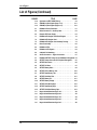
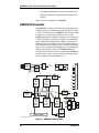
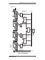
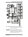
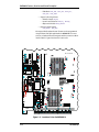
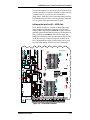
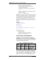
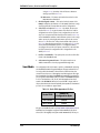
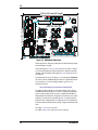
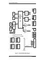
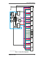
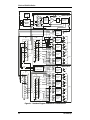
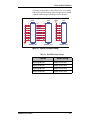
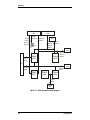
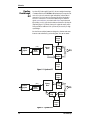
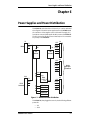
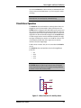
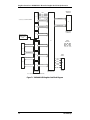
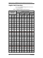
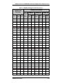
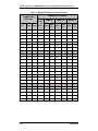
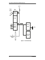
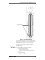
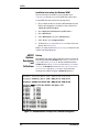
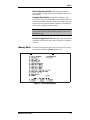
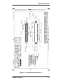
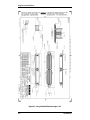
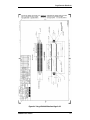
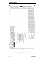
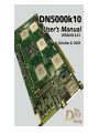
DN5000k10 Features, Overview and General Description
•
User-designed daughter PWB for custom circuitry and interfaces.
•
SignalTap and Identify (from Synplicity) fully supported via JTAG
interface.
Figure 2-1 shows a block diagram of the DN5000k10.
DN5000k10 Description
The DN5000k10 is a complete logic emulation system that enables ASIC or
IP designers a vehicle to prototype logic and memory designs for a fraction
of the cost of existing solutions. The DN5000k10 can be hosted in a 32/64bit PCI/PCI-X slot, or can be used as a stand-alone device. A single
DN5000k10 stuffed with five EP1S80s can emulate up to 3.5 million gates
of logic as measured by LSI. High I/O-count, 1508-pin, flip-chip BGA packages are employed. The F1508 package has 1203 I/Os, which allows for
abundant connections to daughter connectors and external memories. A
total of 488 test pins are provided on the top of the PWB via high-density
connectors for logic analyzer-based debugging, or for pattern generator
stimulus. Custom daughter cards such as the DN3000k10SD can be
mounted to these connectors as a means of interfacing the DN5000k10 to
application-specific circuits. A reference 32-bit PCI target design and test
bench is provided in Verilog at no additional cost.
Smart Media
Card
16/32/64 Mbyte
RS232
EPM3256A
CPLD
32kx8 SRAM
(FPGA configuration
storage)
20
FPGA
Configuration
Switching +3.3V (10A)
Power
+1.5V (10A)
Supply
+5V
ATmega103L
Flash-based µP
FPGA
Configuration
Controller
2
+5V
-12V
+12V
+3.3V
FlowThrough/
Pipelined
ECLK
AB
SSRAM
164
512k x 36
FPGA
A (U12)
FPGA
B (U19)
EP1S80
(FF1508)
EP1S80
(FF1508)
AF
FB
AD
256
153
FB
clocks
FB
512k x 36
BD
AE
144
FlowThrough/
Pipelined
69
MB [255:0]
69
AF
SSRAM
AD
256
ECLK
150
150
15
AD
ECLK
Reset
Control
SSRAM
BE
FlowThrough/
Pipelined
153
21
Top of PWB
AB
AB
69
(test connectors)
+1.5V
190
512k x 36
143
ACLK
FPGA
F (U11)
FE
158
FPGA
E (U15)
EP1S80
(FF1508)
EP1S80
(FF1508)
ED
158
FPGA
D (U20)
BCLK
config
CCLK
EP1S80
(FF1508)
DCLK
110
ECLK
SDRAM
Roboclock
PLL
1
Roboclock
PLL
2
Clock
Selection
Jumpers
or
External
Cable
OSC
X1
OSC
X2
config
92
(168 pin DIMM)
Up to 1GB x 64
69
32/64-Bit PCI/PCI-X
ECLK
FlowThrough/
Pipelined
SSRAM
512k x 36
DN5000k10 REV 10/8/03
DE
Figure 2-1 DN5000k10 Block Diagram
2-2
The DINI Group