1
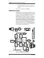
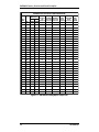
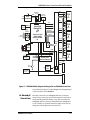
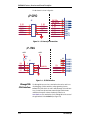
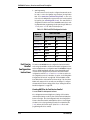
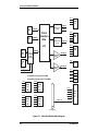
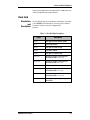
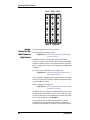
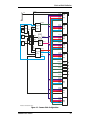
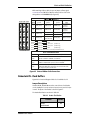
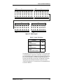
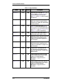
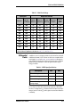
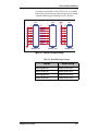
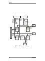
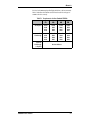
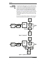
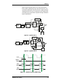
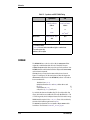
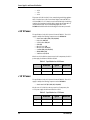
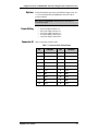
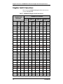
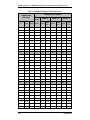
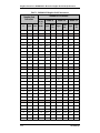
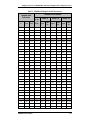
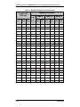
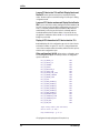
Clocks and Clock Distribution
Table 4-7 Clock Skew Settings
Input Signals
RB[C-F]F1
Output Skew Function
RB[C-F]F0
DCLK[3:0] or DCLK[7:4] or
and FBF0[2:1] ECLK[11:8]
ECLK[15:12]
CCLK[3:0] or
ECLK[3:0]
CCLK[7:4] or
ECLK[7:4]
Feedback
Output
Signals
LOW
LOW
-4tU
-4tU
-8tU
-8tU
-4tU
LOW
MID
-3tU
-3tU
-7tU
-7tU
N/A
LOW
HIGH
-2tU
-2tU
-6tU
-6tU
N/A
MID
LOW
-1tU
-1tU
COL1*
COL1*
N/A
MID
MID
0tU
0tU
0tU
0tU
0tU
MID
HIGH
+1tU
+1tU
COL2**
COL2**
N/A
HIGH
LOW
+2tU
+2tU
+6tU
+6tU
N/A
HIGH
MID
+3tU
+3tU
+7tU
+7tU
N/A
HIGH
HIGH
+4tU
+4tU
+8tU
+8tU
+4tU
*The clock skew is equivalent to the skew on DCLK[3:0] or ECLK[11:8]
**The clock skew is equivalent to the skew on DCLK[7:4] or ECLK[15:12]
Differential
Clocks
In addition to LVTTL clock signals, the RoboclockII clock buffers can handle
LV Differential (LVPECL) clocks. The user can cable in an acceptable differential signal to PLL1B and PLL1BN, or PLL2B and PLL2BN through the
clock grid J13. The signals must obey the specifications given in Table 4-8.
Onboard circuitry is available to center the signals about the proper
voltage, if needed.
Table 4-8 LVPECL Input Specifications
Description
Min
Max
Differential Voltage
0.4
3.3
Highest HIGH Voltage
1.0
3.3
Lowest LOW Voltage
GND
2.9
Common Mode range
(crossing voltage)
0.8
3.3
The clock input of the RoboclockII can accept a superset of PECL. PECL
involves a 1 V swing about VCC/2. The RoboclockII clock input can accept a
swing of up to 3.3 V about VCC/2, which gives the user another dimension
of flexibility.
DN5000k10 User’s Manual
4-13