1
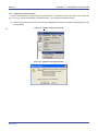
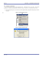
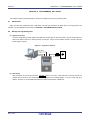
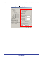
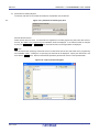
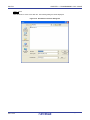
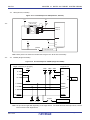
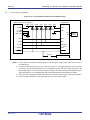
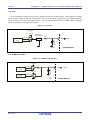
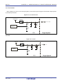
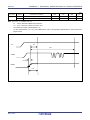
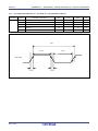
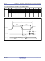
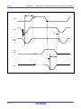
PG-FP5
CHAPTER 12 TROUBLESHOOTING
[Cause 6]
UART communication may not be synchronized.
[Action 6]
When UART is used, communication may not be synchronized due to a baud rate error of the target device. In this
case, change the CPU clock or baud rate, or change the communication channel to another communication mode.
[Cause 7]
If using a 78K0S/Kx1+ microcontroller or the UPD78F9334, it is possible that the wrong connection procedure was
implemented.
[Action 7]
With devices that using program files in which “use the RESET pin as the input-only port (P34)” is set by the option
byte, flash memory programming mode cannot be entered if power is supplied to the target system before the
target cable is connected to the target system. Connect the target cable to the target system and then supply
power to the target system as prescribed in the connection procedure.
<R>
[Cause 8]
For the RX family and Super H family, the I/O signal setting does not match the wiring of the target system.
<R>
[Action 8]
Check if the settings in the [I/O Signal Settings] area on the [Advanced] tab in the Device Setup dialog box match
the wiring of the target system.
(3) The following message is displayed in the action log window and normal communication is not performed in
flash memory programming mode.
ERROR Communication failure or timeout.
[Cause 1]
The clock or power supply may not be stable.
[Action 1]
Confirm that the clock or power is supplied on the target system.
[Cause 2]
Communication may not be stable.
[Action 2]
<1> Confirm that no noise is applied to communication.
<2> Confirm that the FP5 and target system are properly connected.
<3> Confirm that unused pins are properly handled.
<4> Confirm that an appropriate clock and communication rate are selected.
Stable programming may be
achieved by setting a lower value for the clock or communication rate.
R20UT0008EJ0500 Rev. 5.00
2011.12.26
Page 215 of 254