1
SAFETY PRECAUTIONS
(Read these precautions before using this product.)
Before using this product, please read this manual and the relevant manuals carefully and pay full attention
to safety to handle the product correctly.
In this manual, the safety precautions are classified into two levels: "
WARNING" and "
CAUTION".
WARNING
Indicates that incorrect handling may cause hazardous conditions,
resulting in death or severe injury.
CAUTION
Indicates that incorrect handling may cause hazardous conditions,
resulting in minor or moderate injury or property damage.
Under some circumstances, failure to observe the precautions given under "
CAUTION" may lead to
serious consequences.
Observe the precautions of both levels because they are important for personal and system safety.
Make sure that the end users read this manual and then keep the manual in a safe place for future
reference.
[Design Precautions]
WARNING
● Configure safety circuits external to the programmable controller to ensure that the entire system
operates safely even when a fault occurs in the external power supply or the programmable controller.
Failure to do so may result in an accident due to an incorrect output or malfunction.
(1) Configure external safety circuits, such as an emergency stop circuit, protection circuit, and
protective interlock circuit for forward/reverse operation or upper/lower limit positioning.
(2) The programmable controller stops its operation upon detection of the following status, and the
output status of the system will be as shown below.
Overcurrent or overvoltage protection of
the power supply module is activated.
Q series module
AnS/A series module
All outputs are turned off
All outputs are turned off
All outputs are held or turned off
The CPU module detects an error such as a
watchdog timer error by the self-diagnostic function. according to the parameter setting.
All outputs are turned off
All outputs may turn on when an error occurs in the part, such as I/O control part, where the CPU
module cannot detect any error. To ensure safety operation in such a case, provide a safety
mechanism or a fail-safe circuit external to the programmable controller. For a fail-safe circuit
example, refer to Page 638, Appendix 8.
(3) Outputs may remain on or off due to a failure of an output module relay or transistor. Configure an
external circuit for monitoring output signals that could cause a serious accident.
1
[Design Precautions]
WARNING
● In an output module, when a load current exceeding the rated current or an overcurrent caused by a
load short-circuit flows for a long time, it may cause smoke and fire. To prevent this, configure an
external safety circuit, such as a fuse.
● Configure a circuit so that the programmable controller is turned on first and then the external power
supply. If the external power supply is turned on first, an accident may occur due to an incorrect output
or malfunction.
● For the operating status of each station after a communication failure, refer to relevant manuals for the
network. Incorrect output or malfunction due to a communication failure may result in an accident.
● When changing data of the running programmable controller from a peripheral connected to the CPU
module or from a personal computer connected to an intelligent function module, configure an
interlock circuit in the sequence program to ensure that the entire system will always operate safely.
For program modification and operating status change, read relevant manuals carefully and ensure
the safety before operation. Especially, in the case of a control from an external device to a remote
programmable controller, immediate action cannot be taken for a problem on the programmable
controller due to a communication failure. To prevent this, configure an interlock circuit in the
sequence program, and determine corrective actions to be taken between the external device and
CPU module in case of a communication failure.
[Design Precautions]
CAUTION
● Do not install the control lines or communication cables together with the main circuit lines or power
cables. Keep a distance of 100mm (3.94 inches) or more between them. Failure to do so may result in
malfunction due to noise.
● When a device such as a lamp, heater, or solenoid valve is controlled through an output module, a
large current (approximately ten times greater than normal) may flow when the output is turned from
off to on. Take measures such as replacing the module with one having a sufficient current rating.
● After the CPU module is powered on or is reset, the time taken to enter the RUN status varies
depending on the system configuration, parameter settings, and/or program size. Design circuits so
that the entire system will always operate safely, regardless of the time.
2
[Installation Precautions]
CAUTION
● Use the programmable controller in an environment that meets the general specifications in this
manual. Failure to do so may result in electric shock, fire, malfunction, or damage to or deterioration of
the product.
● To mount the module, while pressing the module mounting lever located in the lower part of the
module, fully insert the module fixing projection(s) into the hole(s) in the base unit and press the
module until it snaps into place. Incorrect mounting may cause malfunction, failure or drop of the
module. When using the programmable controller in an environment of frequent vibrations, fix the
module with a screw. Tighten the screw within the specified torque range. Undertightening can cause
drop of the screw, short circuit or malfunction. Overtightening can damage the screw and/or module,
resulting in drop, short circuit, or malfunction.
● When using an extension cable, connect it to the extension cable connector of the base unit securely.
Check the connection for looseness. Poor contact may cause incorrect input or output.
● When using a memory card, fully insert it into the memory card slot. Check that it is inserted
completely. Poor contact may cause malfunction.
● When using an SD memory card, fully insert it into the SD memory card slot. Check that it is inserted
completely. Poor contact may cause malfunction.
● When using an extended SRAM cassette, fully insert it into the connector for cassette connection of
the CPU module. Close the cassette cover after inserting to avoid looseness of the extended SRAM
cassette. Poor contact may cause malfunction.
● Shut off the external power supply (all phases) used in the system before mounting or removing the
module. Failure to do so may result in damage to the product. A module can be replaced online (while
power is on) on any MELSECNET/H remote I/O station or in the system where a CPU module
supporting the online module change function is used. Note that there are restrictions on the modules
that can be replaced online, and each module has its predetermined replacement procedure. For
details, refer to this manual and in the manual for the corresponding module.
● Do not directly touch any conductive part of the module, the memory card, the SD memory card, or
the extended SRAM cassette. Doing so can cause malfunction or failure of the module.
● When using a Motion CPU module and modules designed for motion control, check that the
combinations of these modules are correct before applying power. The modules may be damaged if
the combination is incorrect. For details, refer to the user's manual for the Motion CPU module.
[Wiring Precautions]
WARNING
● Shut off the external power supply (all phases) used in the system before wiring. Failure to do so may
result in electric shock or damage to the product.
● After installation and wiring, attach the included terminal cover to the module before turning it on for
operation. Failure to do so may result in electric shock.
3
[Wiring Precautions]
CAUTION
● Individually ground the FG and LG terminals of the programmable controller with a ground resistance
of 100 or less. Failure to do so may result in electric shock or malfunction.
● Use applicable solderless terminals and tighten them within the specified torque range. If any spade
solderless terminal is used, it may be disconnected when the terminal screw comes loose, resulting in
failure.
● Check the rated voltage and terminal layout before wiring to the module, and connect the cables
correctly. Connecting a power supply with a different voltage rating or incorrect wiring may cause a fire
or failure.
● Connectors for external connection must be crimped or pressed with the tool specified by the
manufacturer, or must be correctly soldered. Incomplete connections could result in short circuit, fire,
or malfunction.
● Install the connector to the module securely. Poor contact may cause malfunction.
● Do not install the control lines or communication cables together with the main circuit lines or power
cables. Keep a distance of 100mm (3.94 inches) or more between them. Failure to do so may result in
malfunction due to noise.
● Place the wires or cables in a duct or clamp them. If not, dangling cable may swing or inadvertently be
pulled, resulting in damage to the module or cables or malfunction due to poor connection.
● Connect the cable correctly after confirming the interface type to be connected. Connecting to the
wrong interface or incorrect wiring can result in a failure of the module or external devices.
● Tighten the terminal screw within the specified torque range. Undertightening can cause short circuit,
fire, or malfunction. Overtightening can damage the screw and/or module, resulting in drop, short
circuit, or malfunction.
● Prevent foreign matter such as dust or wire chips from entering the module. Such foreign matter can
cause a fire, failure, or malfunction.
● A protective film is attached to the top of the module to prevent foreign matter, such as wire chips,
from entering the module during wiring. Do not remove the film during wiring. Remove it for heat
dissipation before system operation.
● Do not pull the cable section of a cable for disconnection. When disconnecting a cable with a
connector, hold the connector and pull it. When disconnecting a cable on a terminal block, loosen the
terminal screw before disconnection. Pulling the connected cable can result in malfunction or damage
of the module or the cable.
● Mitsubishi programmable controllers must be installed in control panels. Connect the main power
supply to the power supply module in the control panel through a relay terminal block. Wiring and
replacement of a power supply module must be performed by maintenance personnel who is familiar
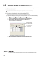
with protection against electric shock. (For wiring methods, refer to Page 100, Section 4.8.1.)
4
[Startup and Maintenance Precautions]
WARNING
● Do not touch any terminal while power is on. Doing so will cause electric shock.
● Correctly connect the battery connector. Do not charge, disassemble, heat, short-circuit, solder, or
throw the battery into the fire, or apply liquid or a strong shock to the battery. Doing so will cause the
battery to produce heat, explode, ignite, or liquid spill, resulting in injury and fire.
● Shut off the external power supply (all phases) used in the system before cleaning the module or
retightening the terminal screws, connector screws, or module fixing screws. Failure to do so may
result in electric shock or cause the module to fail or malfunction.
[Startup and Maintenance Precautions]
CAUTION
● Before performing online operations (especially, program modification, forced output, and operation
status change) for the running CPU module from the peripheral connected, read relevant manuals
carefully and ensure the safety. Improper operation may damage machines or cause accidents.
● Do not disassemble or modify the modules. Doing so may cause failure, malfunction, injury, or a fire.
● Use any radio communication device such as a cellular phone or PHS (Personal Handy-phone
System) more than 25cm (9.85 inches) away in all directions from the programmable controller.
Failure to do so may cause malfunction.
● Shut off the external power supply (all phases) used in the system before mounting or removing the
module. Failure to do so may cause the module to fail or malfunction. A module can be replaced
online (while power is on) on any MELSECNET/H remote I/O station or in the system where a CPU
module supporting the online module change function is used. Note that there are restrictions on the
modules that can be replaced online, and each module has its predetermined replacement procedure.
For details, refer to this manual and the manual for the corresponding module.
● After the first use of the product, do not mount/remove the module to/from the base unit, the extended
SRAM cassette to/from the CPU module, or the terminal block to/from the module more than 50 times
(IEC 61131-2 compliant) respectively. Exceeding the limit of 50 times may cause malfunction.
● After the first use of the product, do not mount/remove the SD memory card more than 500 times.
Exceeding the limit of 500 times may cause malfunction.
● Do not drop or apply shock to the battery to be installed in the module. Doing so may damage the
battery, causing the battery fluid to leak inside the battery. If the battery is dropped or any shock is
applied to it, dispose of it without using.
● Before handling the module, touch a grounded metal object to discharge the static electricity from the
human body. Failure to do so may cause the module to fail or malfunction.
5
[Disposal Precautions]
CAUTION
● When disposing of this product, treat it as industrial waste. When disposing of batteries, separate
them from other wastes according to the local regulations. (For details of the Battery Directive in EU
countries, refer to Page 646, Appendix 11.)
[Transportation Precautions]
CAUTION
● When transporting lithium batteries, follow the transportation regulations. (For details of the regulated
models, refer to Page 645, Appendix 10.)
6
CONDITIONS OF USE FOR THE PRODUCT
(1) Mitsubishi programmable controller ("the PRODUCT") shall be used in conditions;
i) where any problem, fault or failure occurring in the PRODUCT, if any, shall not lead to any major
or serious accident; and
ii) where the backup and fail-safe function are systematically or automatically provided outside of
the PRODUCT for the case of any problem, fault or failure occurring in the PRODUCT.
(2) The PRODUCT has been designed and manufactured for the purpose of being used in general
industries.
MITSUBISHI SHALL HAVE NO RESPONSIBILITY OR LIABILITY (INCLUDING, BUT NOT
LIMITED TO ANY AND ALL RESPONSIBILITY OR LIABILITY BASED ON CONTRACT,
WARRANTY, TORT, PRODUCT LIABILITY) FOR ANY INJURY OR DEATH TO PERSONS OR
LOSS OR DAMAGE TO PROPERTY CAUSED BY the PRODUCT THAT ARE OPERATED OR
USED IN APPLICATION NOT INTENDED OR EXCLUDED BY INSTRUCTIONS, PRECAUTIONS,
OR WARNING CONTAINED IN MITSUBISHI'S USER, INSTRUCTION AND/OR SAFETY
MANUALS, TECHNICAL BULLETINS AND GUIDELINES FOR the PRODUCT.
("Prohibited Application")
Prohibited Applications include, but not limited to, the use of the PRODUCT in;
• Nuclear Power Plants and any other power plants operated by Power companies, and/or any
other cases in which the public could be affected if any problem or fault occurs in the PRODUCT.
• Railway companies or Public service purposes, and/or any other cases in which establishment of
a special quality assurance system is required by the Purchaser or End User.
• Aircraft or Aerospace, Medical applications, Train equipment, transport equipment such as
Elevator and Escalator, Incineration and Fuel devices, Vehicles, Manned transportation,
Equipment for Recreation and Amusement, and Safety devices, handling of Nuclear or
Hazardous Materials or Chemicals, Mining and Drilling, and/or other applications where there is a
significant risk of injury to the public or property.
Notwithstanding the above, restrictions Mitsubishi may in its sole discretion, authorize use of the
PRODUCT in one or more of the Prohibited Applications, provided that the usage of the PRODUCT
is limited only for the specific applications agreed to by Mitsubishi and provided further that no
special quality assurance or fail-safe, redundant or other safety features which exceed the general
specifications of the PRODUCTs are required. For details, please contact the Mitsubishi
representative in your region.
7
INTRODUCTION
This manual provides hardware specifications, maintenance and inspection of the system, and troubleshooting of the CPU
modules, power supply modules, and base units required for operating the Q series programmable controllers.
Before using this product, please read this manual and the relevant manuals carefully and develop familiarity with the
functions and performance of the Q series programmable controller to handle the product correctly.
When applying the program examples introduced in this manual to the actual system, ensure the applicability and confirm that
it will not cause system control problems.
Relevant CPU module
CPU module
Model
Basic model QCPU
Q00(J)CPU, Q01CPU
High Performance model QCPU
Q02(H)CPU, Q06HCPU, Q12HCPU, Q25HCPU
Process CPU
Q02PHCPU, Q06PHCPU, Q12PHCPU, Q25PHCPU
Redundant CPU
Q12PRHCPU, Q25PRHCPU
Q00U(J)CPU, Q01UCPU, Q02UCPU, Q03UD(E)CPU, Q03UDVCPU,
Universal model QCPU
Q04UD(E)HCPU, Q04UDVCPU, Q06UD(E)HCPU, Q06UDVCPU,
Q10UD(E)HCPU, Q13UD(E)HCPU, Q13UDVCPU, Q20UD(E)HCPU,
Q26UD(E)HCPU, Q26UDVCPU, Q50UDEHCPU, Q100UDEHCPU
First use of the Q series CPU module
Memory must be formatted using a programming tool before first use of the CPU module.
For details of memory formatting, refer to the following.
Operating manual for the programming tool used
Precautions for batteries
(1)
When resuming operation with the CPU module which has been stored without battery:
The CPU module memory must be formatted using a programming tool. (
Page 258, Section 13.4)
Remark
This manual does not describe the functions of the CPU module.
For the functions, refer to the following.
Manuals for the CPU module used. (Function Explanation, Program Fundamentals)
For multiple CPU systems, refer to the following.
QCPU User's Manual (Multiple CPU System)
For redundant systems, refer to the following.
QnPRHCPU User's Manual (Redundant System)
8
Memo
9
CONTENTS
CONTENTS
SAFETY PRECAUTIONS . . . . . . . . . . . . . . . . . . . . . . . . . . . . . . . . . . . . . . . . . . . . . . . . . . . . . . . . . . . . . 1
CONDITIONS OF USE FOR THE PRODUCT . . . . . . . . . . . . . . . . . . . . . . . . . . . . . . . . . . . . . . . . . . . . . 7
INTRODUCTION . . . . . . . . . . . . . . . . . . . . . . . . . . . . . . . . . . . . . . . . . . . . . . . . . . . . . . . . . . . . . . . . . . . . 8
MANUALS . . . . . . . . . . . . . . . . . . . . . . . . . . . . . . . . . . . . . . . . . . . . . . . . . . . . . . . . . . . . . . . . . . . . . . . . 15
MANUAL PAGE ORGANIZATION . . . . . . . . . . . . . . . . . . . . . . . . . . . . . . . . . . . . . . . . . . . . . . . . . . . . . . 18
TERMS . . . . . . . . . . . . . . . . . . . . . . . . . . . . . . . . . . . . . . . . . . . . . . . . . . . . . . . . . . . . . . . . . . . . . . . . . . 19
PACKING LIST . . . . . . . . . . . . . . . . . . . . . . . . . . . . . . . . . . . . . . . . . . . . . . . . . . . . . . . . . . . . . . . . . . . . 22
CHAPTER 1 OVERVIEW
1.1
Features . . . . . . . . . . . . . . . . . . . . . . . . . . . . . . . . . . . . . . . . . . . . . . . . . . . . . . . . . . . . . . . . . . 23
CHAPTER 2 SYSTEM CONFIGURATION
30
2.1
Overall Configuration . . . . . . . . . . . . . . . . . . . . . . . . . . . . . . . . . . . . . . . . . . . . . . . . . . . . . . . . 31
2.2
Component List. . . . . . . . . . . . . . . . . . . . . . . . . . . . . . . . . . . . . . . . . . . . . . . . . . . . . . . . . . . . . 32
2.3
Precautions for System Configuration . . . . . . . . . . . . . . . . . . . . . . . . . . . . . . . . . . . . . . . . . . . 35
2.3.1
Bus connection of GOT . . . . . . . . . . . . . . . . . . . . . . . . . . . . . . . . . . . . . . . . . . . . . . . . . . . . . 43
2.3.2
Peripheral device configuration . . . . . . . . . . . . . . . . . . . . . . . . . . . . . . . . . . . . . . . . . . . . . . . 47
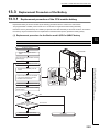
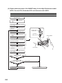
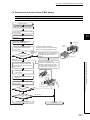
CHAPTER 3 CPU MODULE START-UP PROCEDURES
53
CHAPTER 4 INSTALLATION AND WIRING
55
4.1
4.2
4.3
Installation Environment and Installation Position . . . . . . . . . . . . . . . . . . . . . . . . . . . . . . . . . . 55
4.1.1
Installation environment . . . . . . . . . . . . . . . . . . . . . . . . . . . . . . . . . . . . . . . . . . . . . . . . . . . . . 55
4.1.2
Instructions for mounting the base unit . . . . . . . . . . . . . . . . . . . . . . . . . . . . . . . . . . . . . . . . . 56
Module Installation . . . . . . . . . . . . . . . . . . . . . . . . . . . . . . . . . . . . . . . . . . . . . . . . . . . . . . . . . . 59
4.2.1
Precaution on installation . . . . . . . . . . . . . . . . . . . . . . . . . . . . . . . . . . . . . . . . . . . . . . . . . . . . 59
4.2.2
Base unit installation . . . . . . . . . . . . . . . . . . . . . . . . . . . . . . . . . . . . . . . . . . . . . . . . . . . . . . . 60
4.2.3
Installation and removal of module . . . . . . . . . . . . . . . . . . . . . . . . . . . . . . . . . . . . . . . . . . . . 67
Connecting an Extension Base Unit . . . . . . . . . . . . . . . . . . . . . . . . . . . . . . . . . . . . . . . . . . . . . 74
4.3.1
Setting the extension base number . . . . . . . . . . . . . . . . . . . . . . . . . . . . . . . . . . . . . . . . . . . . 74
4.3.2
Connection and disconnection of extension cable . . . . . . . . . . . . . . . . . . . . . . . . . . . . . . . . . 81
4.3.3
Extension cable specifications . . . . . . . . . . . . . . . . . . . . . . . . . . . . . . . . . . . . . . . . . . . . . . . . 83
4.3.4
Voltage drop when an extension base unit is used . . . . . . . . . . . . . . . . . . . . . . . . . . . . . . . . 84
4.4
Mounting and Removing a Terminal Block . . . . . . . . . . . . . . . . . . . . . . . . . . . . . . . . . . . . . . . . 90
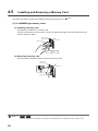
4.5
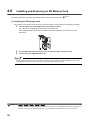
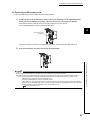
Installing and Removing a Memory Card . . . . . . . . . . . . . . . . . . . . . . . . . . . . . . . . . . . . . . . . . 92
4.6
Installing and Removing an SD Memory Card . . . . . . . . . . . . . . . . . . . . . . . . . . . . . . . . . . . . . 96
4.7
Installing and Removing an Extended SRAM Cassette . . . . . . . . . . . . . . . . . . . . . . . . . . . . . . 98
4.8
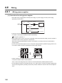
Wiring . . . . . . . . . . . . . . . . . . . . . . . . . . . . . . . . . . . . . . . . . . . . . . . . . . . . . . . . . . . . . . . . . . . 100
4.8.1
Wiring power supplies . . . . . . . . . . . . . . . . . . . . . . . . . . . . . . . . . . . . . . . . . . . . . . . . . . . . . 100
4.8.2
Wiring of 18-point screw terminal block . . . . . . . . . . . . . . . . . . . . . . . . . . . . . . . . . . . . . . . . 105
4.8.3
Wiring to connectors . . . . . . . . . . . . . . . . . . . . . . . . . . . . . . . . . . . . . . . . . . . . . . . . . . . . . . 107
4.8.4
Grounding . . . . . . . . . . . . . . . . . . . . . . . . . . . . . . . . . . . . . . . . . . . . . . . . . . . . . . . . . . . . . . 112
CHAPTER 5 GENERAL SPECIFICATIONS
10
23
113
CHAPTER 6 CPU MODULE
6.1
6.2
6.3
6.4
6.5
6.6
Part Names. . . . . . . . . . . . . . . . . . . . . . . . . . . . . . . . . . . . . . . . . . . . . . . . . . . . . . . . . . . . . . . 115
6.1.1
Basic model QCPU . . . . . . . . . . . . . . . . . . . . . . . . . . . . . . . . . . . . . . . . . . . . . . . . . . . . . . . 115
6.1.2
High Performance model QCPU, Process CPU and Redundant CPU . . . . . . . . . . . . . . . . 121
6.1.3
Universal model QCPU . . . . . . . . . . . . . . . . . . . . . . . . . . . . . . . . . . . . . . . . . . . . . . . . . . . . 126
Specifications . . . . . . . . . . . . . . . . . . . . . . . . . . . . . . . . . . . . . . . . . . . . . . . . . . . . . . . . . . . . . 141
6.2.1
Basic model QCPU . . . . . . . . . . . . . . . . . . . . . . . . . . . . . . . . . . . . . . . . . . . . . . . . . . . . . . . 141
6.2.2
High Performance model QCPU . . . . . . . . . . . . . . . . . . . . . . . . . . . . . . . . . . . . . . . . . . . . . 144
6.2.3
Process CPU . . . . . . . . . . . . . . . . . . . . . . . . . . . . . . . . . . . . . . . . . . . . . . . . . . . . . . . . . . . . 148
6.2.4
Redundant CPU . . . . . . . . . . . . . . . . . . . . . . . . . . . . . . . . . . . . . . . . . . . . . . . . . . . . . . . . . . 152
6.2.5
Universal model QCPU . . . . . . . . . . . . . . . . . . . . . . . . . . . . . . . . . . . . . . . . . . . . . . . . . . . . 156
Switch Operation at the Time of Writing Program. . . . . . . . . . . . . . . . . . . . . . . . . . . . . . . . . . 175
6.3.1
Basic model QCPU and Universal model QCPU . . . . . . . . . . . . . . . . . . . . . . . . . . . . . . . . . 175
6.3.2
High Performance model QCPU, Process CPU and Redundant CPU . . . . . . . . . . . . . . . . 176
Reset Operation . . . . . . . . . . . . . . . . . . . . . . . . . . . . . . . . . . . . . . . . . . . . . . . . . . . . . . . . . . . 177
6.4.1
Basic model QCPU and Universal model QCPU . . . . . . . . . . . . . . . . . . . . . . . . . . . . . . . . . 177
6.4.2
High Performance model QCPU, Process CPU and Redundant CPU . . . . . . . . . . . . . . . . 178
Latch Clear Operation. . . . . . . . . . . . . . . . . . . . . . . . . . . . . . . . . . . . . . . . . . . . . . . . . . . . . . . 179
6.5.1
Basic model QCPU and Universal model QCPU . . . . . . . . . . . . . . . . . . . . . . . . . . . . . . . . . 179
6.5.2
High Performance model QCPU, Process CPU and Redundant CPU . . . . . . . . . . . . . . . . 179
Automatic Write to the Standard ROM . . . . . . . . . . . . . . . . . . . . . . . . . . . . . . . . . . . . . . . . . . 180
CHAPTER 7 POWER SUPPLY MODULE
7.1
182
Part Names and Settings . . . . . . . . . . . . . . . . . . . . . . . . . . . . . . . . . . . . . . . . . . . . . . . . . . . . 183
7.1.1
7.2
115
Base unit that can be used in combination with power supply module . . . . . . . . . . . . . . . . 189
Specifications . . . . . . . . . . . . . . . . . . . . . . . . . . . . . . . . . . . . . . . . . . . . . . . . . . . . . . . . . . . . . 191
7.2.1
Power supply module specifications . . . . . . . . . . . . . . . . . . . . . . . . . . . . . . . . . . . . . . . . . . 191
7.2.2
Specifications . . . . . . . . . . . . . . . . . . . . . . . . . . . . . . . . . . . . . . . . . . . . . . . . . . . . . . . . . . . . 208
7.2.3
Selecting the power supply module . . . . . . . . . . . . . . . . . . . . . . . . . . . . . . . . . . . . . . . . . . . 209
7.2.4
Precautions on power supply capacity. . . . . . . . . . . . . . . . . . . . . . . . . . . . . . . . . . . . . . . . . 212
7.2.5
Life detection power supply module. . . . . . . . . . . . . . . . . . . . . . . . . . . . . . . . . . . . . . . . . . . 213
CHAPTER 8 BASE UNIT
217
8.1
Part Names. . . . . . . . . . . . . . . . . . . . . . . . . . . . . . . . . . . . . . . . . . . . . . . . . . . . . . . . . . . . . . . 217
8.2
Extension Base Units that can be Combined with the Main Base Unit. . . . . . . . . . . . . . . . . . 224
8.3
Specification Table . . . . . . . . . . . . . . . . . . . . . . . . . . . . . . . . . . . . . . . . . . . . . . . . . . . . . . . . . 225
CHAPTER 9 MEMORY CARD
9.1
Part Names. . . . . . . . . . . . . . . . . . . . . . . . . . . . . . . . . . . . . . . . . . . . . . . . . . . . . . . . . . . . . . . 229
9.1.1
9.2
9.3
229
List of usable memory cards . . . . . . . . . . . . . . . . . . . . . . . . . . . . . . . . . . . . . . . . . . . . . . . . 230
Specifications . . . . . . . . . . . . . . . . . . . . . . . . . . . . . . . . . . . . . . . . . . . . . . . . . . . . . . . . . . . . . 231
9.2.1
Memory card specifications . . . . . . . . . . . . . . . . . . . . . . . . . . . . . . . . . . . . . . . . . . . . . . . . . 231
9.2.2
Specifications of the memory card battery . . . . . . . . . . . . . . . . . . . . . . . . . . . . . . . . . . . . . . 233
Handling . . . . . . . . . . . . . . . . . . . . . . . . . . . . . . . . . . . . . . . . . . . . . . . . . . . . . . . . . . . . . . . . . 234
11
9.3.1
Battery installation into the memory card . . . . . . . . . . . . . . . . . . . . . . . . . . . . . . . . . . . . . . . 235
CHAPTER 10 SD MEMORY CARD
237
10.1
Part Names. . . . . . . . . . . . . . . . . . . . . . . . . . . . . . . . . . . . . . . . . . . . . . . . . . . . . . . . . . . . . . . 237
10.2
Specifications . . . . . . . . . . . . . . . . . . . . . . . . . . . . . . . . . . . . . . . . . . . . . . . . . . . . . . . . . . . . . 238
10.3
Handling . . . . . . . . . . . . . . . . . . . . . . . . . . . . . . . . . . . . . . . . . . . . . . . . . . . . . . . . . . . . . . . . . 238
10.4
Forcibly Disabling the SD Memory Card. . . . . . . . . . . . . . . . . . . . . . . . . . . . . . . . . . . . . . . . . 239
CHAPTER 11 EXTENDED SRAM CASSETTE
240
11.1
Part Names. . . . . . . . . . . . . . . . . . . . . . . . . . . . . . . . . . . . . . . . . . . . . . . . . . . . . . . . . . . . . . . 240
11.2
Specifications . . . . . . . . . . . . . . . . . . . . . . . . . . . . . . . . . . . . . . . . . . . . . . . . . . . . . . . . . . . . . 241
11.3
Handling . . . . . . . . . . . . . . . . . . . . . . . . . . . . . . . . . . . . . . . . . . . . . . . . . . . . . . . . . . . . . . . . . 241
CHAPTER 12 BATTERY
242
12.1
Battery Specifications . . . . . . . . . . . . . . . . . . . . . . . . . . . . . . . . . . . . . . . . . . . . . . . . . . . . . . . 242
12.2
Battery Installation . . . . . . . . . . . . . . . . . . . . . . . . . . . . . . . . . . . . . . . . . . . . . . . . . . . . . . . . . 243
CHAPTER 13 MAINTENANCE AND INSPECTION
247
13.1
Daily Inspection . . . . . . . . . . . . . . . . . . . . . . . . . . . . . . . . . . . . . . . . . . . . . . . . . . . . . . . . . . . 247
13.2
Periodic Inspection . . . . . . . . . . . . . . . . . . . . . . . . . . . . . . . . . . . . . . . . . . . . . . . . . . . . . . . . . 248
13.3
Replacement Procedure of the Battery. . . . . . . . . . . . . . . . . . . . . . . . . . . . . . . . . . . . . . . . . . 249
13.3.1 Replacement procedure of the CPU module battery . . . . . . . . . . . . . . . . . . . . . . . . . . . . . . 249
13.3.2 SRAM card battery replacement procedure. . . . . . . . . . . . . . . . . . . . . . . . . . . . . . . . . . . . . 255
13.4
Operating the Programmable Controller that Has been Stored . . . . . . . . . . . . . . . . . . . . . . . 258
CHAPTER 14 MODULE CHANGE DURING SYSTEM OPERATION
259
14.1
Online Module Change . . . . . . . . . . . . . . . . . . . . . . . . . . . . . . . . . . . . . . . . . . . . . . . . . . . . . . 259
14.2
Change of Redundant Power Supply Module. . . . . . . . . . . . . . . . . . . . . . . . . . . . . . . . . . . . . 269
CHAPTER 15 TROUBLESHOOTING
15.1
270
Visual Inspection. . . . . . . . . . . . . . . . . . . . . . . . . . . . . . . . . . . . . . . . . . . . . . . . . . . . . . . . . . . 271
15.1.1 When the POWER LED does not turn on . . . . . . . . . . . . . . . . . . . . . . . . . . . . . . . . . . . . . . 272
15.1.2 When the POWER LED does not turn on in green . . . . . . . . . . . . . . . . . . . . . . . . . . . . . . . 272
15.1.3 When the LIFE LED does not turn on in green or orange . . . . . . . . . . . . . . . . . . . . . . . . . . 273
15.1.4 When the MODE LED does not turn on . . . . . . . . . . . . . . . . . . . . . . . . . . . . . . . . . . . . . . . . 274
15.1.5 When the RUN LED does not turn on . . . . . . . . . . . . . . . . . . . . . . . . . . . . . . . . . . . . . . . . . 275
15.1.6 When the BOOT LED flickers . . . . . . . . . . . . . . . . . . . . . . . . . . . . . . . . . . . . . . . . . . . . . . . 275
15.2
Checking the Error Details . . . . . . . . . . . . . . . . . . . . . . . . . . . . . . . . . . . . . . . . . . . . . . . . . . . 276
15.3
Checking for Functional Errors . . . . . . . . . . . . . . . . . . . . . . . . . . . . . . . . . . . . . . . . . . . . . . . . 279
15.3.1 Write to PLC and Read from PLC . . . . . . . . . . . . . . . . . . . . . . . . . . . . . . . . . . . . . . . . . . . . 280
15.3.2 Boot operation . . . . . . . . . . . . . . . . . . . . . . . . . . . . . . . . . . . . . . . . . . . . . . . . . . . . . . . . . . . 281
15.3.3 Errors caused by hardware . . . . . . . . . . . . . . . . . . . . . . . . . . . . . . . . . . . . . . . . . . . . . . . . . 282
15.3.4 Ethernet communication . . . . . . . . . . . . . . . . . . . . . . . . . . . . . . . . . . . . . . . . . . . . . . . . . . . 283
12
15.3.5 Socket communication function . . . . . . . . . . . . . . . . . . . . . . . . . . . . . . . . . . . . . . . . . . . . . . 288
15.3.6 MC protocol function . . . . . . . . . . . . . . . . . . . . . . . . . . . . . . . . . . . . . . . . . . . . . . . . . . . . . . 289
15.3.7 Transmission from an external device . . . . . . . . . . . . . . . . . . . . . . . . . . . . . . . . . . . . . . . . . 290
15.3.8 Operating status of the CPU module . . . . . . . . . . . . . . . . . . . . . . . . . . . . . . . . . . . . . . . . . . 290
15.3.9 Errors caused by SFC program instruction . . . . . . . . . . . . . . . . . . . . . . . . . . . . . . . . . . . . . 291
15.3.10 I/O module . . . . . . . . . . . . . . . . . . . . . . . . . . . . . . . . . . . . . . . . . . . . . . . . . . . . . . . . . . . . . . 292
15.3.11 Power supply module. . . . . . . . . . . . . . . . . . . . . . . . . . . . . . . . . . . . . . . . . . . . . . . . . . . . . . 293
15.4
Saving Data . . . . . . . . . . . . . . . . . . . . . . . . . . . . . . . . . . . . . . . . . . . . . . . . . . . . . . . . . . . . . . 295
APPENDICES
299
Appendix 1 Error Code Lists . . . . . . . . . . . . . . . . . . . . . . . . . . . . . . . . . . . . . . . . . . . . . . . . . . . . . . 299
Appendix 1.1
Error codes . . . . . . . . . . . . . . . . . . . . . . . . . . . . . . . . . . . . . . . . . . . . . . 300
Appendix 1.2
Reading error codes . . . . . . . . . . . . . . . . . . . . . . . . . . . . . . . . . . . . . . . . 300
Appendix 1.3
Error code list (1000 to 1999) . . . . . . . . . . . . . . . . . . . . . . . . . . . . . . . . . . 301
Appendix 1.4
Error code list (2000 to 2999) . . . . . . . . . . . . . . . . . . . . . . . . . . . . . . . . . . 319
Appendix 1.5
Error code list (3000 to 3999) . . . . . . . . . . . . . . . . . . . . . . . . . . . . . . . . . . 345
Appendix 1.6
Error code list (4000 to 4999) . . . . . . . . . . . . . . . . . . . . . . . . . . . . . . . . . . 364
Appendix 1.7
Error code list (5000 to 5999) . . . . . . . . . . . . . . . . . . . . . . . . . . . . . . . . . . 379
Appendix 1.8
Error code list (6000 to 6999) . . . . . . . . . . . . . . . . . . . . . . . . . . . . . . . . . . 381
Appendix 1.9
Error code list (7000 to 10000) . . . . . . . . . . . . . . . . . . . . . . . . . . . . . . . . . . 390
Appendix 1.10 Clearing an error . . . . . . . . . . . . . . . . . . . . . . . . . . . . . . . . . . . . . . . . . . . 394
Appendix 1.11
Error codes returned to request source during communication with CPU module . 395
Appendix 2 Special Relay List. . . . . . . . . . . . . . . . . . . . . . . . . . . . . . . . . . . . . . . . . . . . . . . . . . . . . 429
Appendix 3 Special Register List. . . . . . . . . . . . . . . . . . . . . . . . . . . . . . . . . . . . . . . . . . . . . . . . . . . 478
Appendix 4 Battery Life . . . . . . . . . . . . . . . . . . . . . . . . . . . . . . . . . . . . . . . . . . . . . . . . . . . . . . . . . . 570
Appendix 4.1
Display of battery consumption and reduction measures of the consumption . . . 571
Appendix 4.2
Battery lives of CPU modules . . . . . . . . . . . . . . . . . . . . . . . . . . . . . . . . . . 573
Appendix 4.3
SRAM card battery life . . . . . . . . . . . . . . . . . . . . . . . . . . . . . . . . . . . . . . . 600
Appendix 5 Checking Serial Number and Function Version . . . . . . . . . . . . . . . . . . . . . . . . . . . . . . 602
Appendix 5.1
Applicable software versions . . . . . . . . . . . . . . . . . . . . . . . . . . . . . . . . . . . 604
Appendix 5.2
GX Configurator versions applicable to a single CPU system . . . . . . . . . . . . . . 605
Appendix 6 Added or Changed Functions . . . . . . . . . . . . . . . . . . . . . . . . . . . . . . . . . . . . . . . . . . . 607
Appendix 6.1
Basic model QCPU upgrade . . . . . . . . . . . . . . . . . . . . . . . . . . . . . . . . . . . 607
Appendix 6.2
High Performance model QCPU upgrade . . . . . . . . . . . . . . . . . . . . . . . . . . . 609
Appendix 6.3
Precautions for using older versions of the High Performance model QCPU . . . . 611
Appendix 6.4
Process CPU upgrade . . . . . . . . . . . . . . . . . . . . . . . . . . . . . . . . . . . . . . . 614
Appendix 6.5
Redundant CPU upgrade . . . . . . . . . . . . . . . . . . . . . . . . . . . . . . . . . . . . . 615
Appendix 6.6
Universal model QCPU upgrade . . . . . . . . . . . . . . . . . . . . . . . . . . . . . . . . 616
Appendix 7 EMC and Low Voltage Directives. . . . . . . . . . . . . . . . . . . . . . . . . . . . . . . . . . . . . . . . . 619
Appendix 7.1
Requirements for compliance with the EMC Directive . . . . . . . . . . . . . . . . . . . 619
Appendix 7.1.1
Standards relevant to the EMC Directive . . . . . . . . . . . . . . . . . . . . . . 620
Appendix 7.1.2
Installation instructions for EMC Directive . . . . . . . . . . . . . . . . . . . . . . 622
Appendix 7.1.3
Cables. . . . . . . . . . . . . . . . . . . . . . . . . . . . . . . . . . . . . . . . . . . . . 623
Appendix 7.1.4
Installation environment of the CC-Link/LT module and the AS-i module . 630
Appendix 7.1.5
Power supply part of the power supply module, Q00JCPU, and Q00UJCPU
. . . . . . . . . . . . . . . . . . . . . . . . . . . . . . . . . . . . . . . . . . . . . . . . . . 630
13
Appendix 7.1.6
When using MELSEC-A series modules . . . . . . . . . . . . . . . . . . . . . . 631
Appendix 7.1.7
Others . . . . . . . . . . . . . . . . . . . . . . . . . . . . . . . . . . . . . . . . . . . . . 633
Appendix 7.2
Requirements to compliance with the Low Voltage Directive . . . . . . . . . . . . . . 635
Appendix 7.2.1
Standard applied for MELSEC-Q series programmable controller . . . . . . 635
Appendix 7.2.2
MELSEC-Q series programmable controller selection . . . . . . . . . . . . . . 635
Appendix 7.2.3
Power supply . . . . . . . . . . . . . . . . . . . . . . . . . . . . . . . . . . . . . . . . 636
Appendix 7.2.4
Control panel . . . . . . . . . . . . . . . . . . . . . . . . . . . . . . . . . . . . . . . . 636
Appendix 7.2.5
Grounding . . . . . . . . . . . . . . . . . . . . . . . . . . . . . . . . . . . . . . . . . . 637
Appendix 7.2.6
External wiring . . . . . . . . . . . . . . . . . . . . . . . . . . . . . . . . . . . . . . . 637
Appendix 8 General Safety Requirements . . . . . . . . . . . . . . . . . . . . . . . . . . . . . . . . . . . . . . . . . . . 638
Appendix 9 Calculating Heat Generation of Programmable Controller. . . . . . . . . . . . . . . . . . . . . . 642
Appendix 10 Precautions for Battery Transportation. . . . . . . . . . . . . . . . . . . . . . . . . . . . . . . . . . . . . 645
Appendix 11 Handling of Batteries and Devices with Built-in Batteries in EU Member States . . . . . 646
Appendix 11.1
Disposal precautions . . . . . . . . . . . . . . . . . . . . . . . . . . . . . . . . . . . . . . . . 646
Appendix 11.2
Exportation precautions . . . . . . . . . . . . . . . . . . . . . . . . . . . . . . . . . . . . . . 647
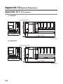
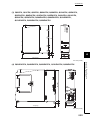
Appendix 12 External Dimensions . . . . . . . . . . . . . . . . . . . . . . . . . . . . . . . . . . . . . . . . . . . . . . . . . . 648
Appendix 12.1 CPU modules . . . . . . . . . . . . . . . . . . . . . . . . . . . . . . . . . . . . . . . . . . . . . 648
Appendix 12.2 Power supply modules . . . . . . . . . . . . . . . . . . . . . . . . . . . . . . . . . . . . . . . 653
Appendix 12.3 Main base units . . . . . . . . . . . . . . . . . . . . . . . . . . . . . . . . . . . . . . . . . . . 657
Appendix 12.4 Extension base units . . . . . . . . . . . . . . . . . . . . . . . . . . . . . . . . . . . . . . . . 663
Appendix 12.5 Other optional items. . . . . . . . . . . . . . . . . . . . . . . . . . . . . . . . . . . . . . . . . 669
INDEX
671
REVISIONS . . . . . . . . . . . . . . . . . . . . . . . . . . . . . . . . . . . . . . . . . . . . . . . . . . . . . . . . . . . . . . . . . . . . . . 675
WARRANTY . . . . . . . . . . . . . . . . . . . . . . . . . . . . . . . . . . . . . . . . . . . . . . . . . . . . . . . . . . . . . . . . . . . . . 679
14
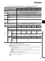
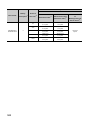
MANUALS
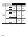
To understand the main specifications, functions, and usage of the CPU module, refer to the basic manuals.
Read other manuals as well when using a different type of CPU module and its functions.
Order each manual as needed, referring to the following lists.
The numbers in the "CPU module" and the respective modules are as follows.
Number
CPU module
1)
Basic model QCPU
2)
High Performance model QCPU
3)
Process CPU
4)
Redundant CPU
5)
Universal model QCPU
● : Basic manual,
: Other CPU module manuals/Use them to utilize functions.
(1) CPU module user's manual
Manual name
Description
< Manual number (model code) >
QnUCPU Users Manual (Function Explanation,
Program Fundamentals)
< SH-080807ENG (13JZ27) >
Qn(H)/QnPH/QnPRHCPU User's Manual (Function
Explanation, Program Fundamentals)
< SH-080808ENG (13JZ28) >
QCPU User's Manual (Multiple CPU System)
CPU module
1)
2)
3)
4)
Functions, methods, and devices for
●
programming
Functions, methods, and devices for
programming
5)
●
●
●
●
Information for configuring a multiple CPU
system (system configuration, I/O numbers,
communication between CPU modules, and
communication with the input/output modules
< SH-080485ENG (13JR75) >
QnPRHCPU User's Manual (Redundant System)
and intelligent function modules)
Redundant system configuration, functions,
communication with external devices, and
< SH-080486ENG (13JR76) >
QnUCPU User's Manual (Communication via Built-in
Ethernet Port)
< SH-080811ENG (13JZ29) >
QnUDVCPU/LCPU User's Manual (Data Logging
Function)
< SH-080893ENG (13JZ39) >
●
troubleshooting
Functions for the communication via built-in
Ethernet port
Functions for the data logging of the CPU
module
15
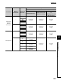
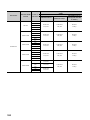
(2) Programming manual
Manual name
Description
< Manual number (model code) >
MELSEC-Q/L Programming Manual (Common
Instruction)
< SH-080809ENG (13JW10) >
MELSEC-Q/L/QnA Programming Manual (SFC)
How to use sequence instructions, basic
instructions, and application instructions
CPU module
1)
2)
3)
4)
5)
●
●
●
●
●
System configuration, performance
specifications, functions, programming,
debugging, and error codes for SFC
< SH-080041 (13JF60) >
MELSEC-Q/L Programming Manual (MELSAP-L)
< SH-080076 (13JF61) >
MELSEC-Q/L Programming Manual (Structured
Text)
< SH-080366E (13JF68) >
(MELSAP3) programs
Programming methods, specifications, and
functions for SFC (MELSAP-L) programs
Programming methods using structured text
language
MELSEC-Q/L/QnA Programming Manual (PID
Control Instructions)
Dedicated instructions for PID control
< SH-080040 (13JF59) >
QnPHCPU/QnPRHCPU Programming Manual
(Process Control Instructions)
Dedicated instructions for process control
< SH-080316E (13JF67) >
(3) Operating manual
Manual name
Description
< Manual number (model code) >
GX Works2 Version1 Operating Manual (Common)
Operating methods of GX Developer, such as
programming, printing, monitoring, and
<SH-080373E, 13JU41>
16
1)
2)
3)
4)
5)
●
●
●
●
●
System configuration, parameter settings, and
online operations (common to Simple project
<SH-080779ENG, 13JU63> and Structured project) of GX Works2
GX Developer Version 8 Operating Manual
CPU module
debugging
(4) Intelligent function module manual
Manual name
Description
< Manual number (model code) >
CC-Link IE Controller Network Reference Manual
CPU module
1)
2)
3)
4)
5)
Specifications, procedures and settings before
system operation, parameter setting,
programming, and troubleshooting of the CC-
< SH-080668ENG (13JV16) >
Link IE Controller Network module
MELSEC-Q CC-Link IE Field Network Master/Local
Specifications, procedures and settings before
Module User's Manual
system operation, parameter setting,
programming, and troubleshooting of the CC< SH-080917ENG (13JZ47) >
Link IE Field Network module
Q Corresponding MELSECNET/H Network System
Specifications, procedures and settings before
Reference Manual (PLC to PLC network)
system operation, parameter setting,
programming, and troubleshooting of a
MELSECNET/H network system (PLC to PLC
< SH-080049 (13JF92) >
network)
Q Corresponding MELSECNET/H Network System
Specifications, procedures and settings before
Reference Manual (Remote I/O network)
system operation, parameter setting,
programming, and troubleshooting of a
MELSECNET/H network system (remote I/O
< SH-080124 (13JF96) >
network)
Q Corresponding Ethernet Interface Module User's
Specifications, procedures for data
Manual (Basic)
communication with external devices, line
connection (open/close), fixed buffer
communication, random access buffer
communication, and troubleshooting of the
< SH-080009 (13JL88) >
Ethernet module
MELSEC-Q/L Ethernet Interface Module User's
E-mail function, programmable controller CPU
Manual (Application)
status monitoring function, communication via
CC-Link IE Controller Network, CC-Link IE
Field Network, MELSECNET/H, or
MELSECNET/10, communication using the
data link instructions, and file transfer function
< SH-080010 (13JL89) >
(FTP server) of the Ethernet module
MELSEC-Q CC-Link System Master/Local Module
System configuration, performance
User's Manual
specifications, functions, handling, wiring, and
< SH-080394E (13JR64) >
troubleshooting of the QJ61BT11N
Q Corresponding Serial Communication Module
Overview, system configuration, specifications,
User's Manual (Basic)
procedures before operation, basic data
communication method with external devices,
maintenance and inspection, and
troubleshooting for using the serial
< SH-080006 (13JL86) >
communication module
MELSEC-Q/L Serial Communication Module User's
Special functions (specifications, usage, and
Manual (Application)
settings) and data communication method with
external devices of the serial communication
< SH-080007 (13JL87) >
module
17
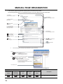
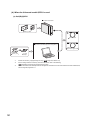
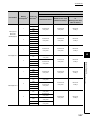
MANUAL PAGE ORGANIZATION
In this manual, pages are organized and the symbols are used as shown below.
The following page illustration is for explanation purpose only, and is different from the actual pages
"" is used for
screen names and items.
The chapter of
the current page is shown.
shows operating
procedures.
shows mouse
operations.*1
[ ] is used for items
in the menu bar and
the project window.
The section of
the current page is shown.
Ex. shows setting or
operating examples.
shows reference
manuals.
shows notes that
requires attention.
shows
reference pages.
shows useful
information.
*1
The mouse operation example is provided below. (For GX Works2)
Menu bar
Ex.
[Online]
[Write to PLC...]
Select [Online] on the menu bar,
and then select [Write to PLC...].
A window selected in the view selection area is displayed.
Ex.
[Parameter]
Project window
[PLC Parameter]
Select [Project] from the view selection
area to open the Project window.
In the Project window, expand [Parameter] and
select [PLC Parameter].
View selection area
Icons
Basic model
QCPU
Basic
18
High
Performance
model QCPU
High
performance
Process
Redundant
Universal model
CPU
CPU
QCPU
Process
Redundant
Universal
Description
Icons indicate that specifications described
on the page contain some precautions.
TERMS
Unless otherwise specified, this manual uses the following generic terms and abbreviations.
* indicates a part of the model or version.
(Example): Q33B, Q35B, Q38B, Q312B Q3B
Term
Description
Series
Q series
Abbreviation for Mitsubishi MELSEC-Q series programmable controller
AnS series
Abbreviation for compact types of Mitsubishi MELSEC-A Series Programmable Controller
A series
Abbreviation for large types of Mitsubishi MELSEC-A Series Programmable Controller
CPU module type
CPU module
Generic term for the Basic model QCPU, High Performance model QCPU, Process CPU,
Redundant CPU, Universal model QCPU
Basic model QCPU
Generic term for the Q00JCPU, Q00CPU, and Q01CPU
High Performance model QCPU
Generic term for the Q02CPU, Q02HCPU, Q06HCPU, Q12HCPU, Q25HCPU
Process CPU
Generic term for the Q02PHCPU, Q06PHCPU, Q12PHCPU, Q25PHCPU
Redundant CPU
Generic term for the Q12PRHCPU and Q25PRHCPU
Generic term for the Q00UJCPU, Q00UCPU, Q01UCPU, Q02UCPU, Q03UDCPU,
Q03UDVCPU, Q03UDECPU, Q04UDHCPU, Q04UDVCPU, Q04UDEHCPU, Q06UDHCPU,
Universal model QCPU
Q06UDVCPU, Q06UDEHCPU, Q10UDHCPU, Q10UDEHCPU, Q13UDHCPU, Q13UDVCPU,
Q13UDEHCPU, Q20UDHCPU, Q20UDEHCPU, Q26UDHCPU, Q26UDVCPU, Q26UDEHCPU,
Q50UDEHCPU, and Q100UDEHCPU
Generic term for Mitsubishi motion controllers, Q172CPUN, Q173CPUN, Q172HCPU,
Motion CPU
Q173HCPU, Q172CPUN-T, Q173CPUN-T, Q172HCPU-T, Q173HCPU-T, Q172DCPU,
Q173DCPU, Q172DCPU-S1, Q173DCPU-S1, Q172DSCPU, and Q173DSCPU
PC CPU module
C Controller module
High-speed Universal model QCPU
Generic term for MELSEC-Q series-compatible PC CPU module, PPC-CPU852(MS)-512,
manufactured by CONTEC Co., Ltd.
Generic term for the Q06CCPU-V-H01, Q06CCPU-V, Q06CCPU-V-B, Q12DCCPU-V, and
Q24DHCCPU-V C Controller modules
Generic term for the Q03UDVCPU, Q04UDVCPU, Q06UDVCPU, Q13UDVCPU, and
Q26UDVCPU
Generic term for the Q03UDVCPU, Q03UDECPU, Q04UDVCPU, Q04UDEHCPU,
Built-in Ethernet port QCPU
Q06UDVCPU, Q06UDEHCPU, Q10UDEHCPU, Q13UDVCPU, Q13UDEHCPU,
Q20UDEHCPU, Q26UDVCPU, Q26UDEHCPU, Q50UDEHCPU, and Q100UDEHCPU
CPU module model
QnU(D)(H)CPU
QnUDVCPU
QnUDE(H)CPU
Generic term for the Q00UJCPU, Q00UCPU, Q01UCPU, Q02UCPU, Q03UDCPU,
Q04UDHCPU, Q06UDHCPU, Q10UDHCPU, Q13UDHCPU, Q20UDHCPU, and Q26UDHCPU
Generic term for the Q03UDVCPU, Q04UDVCPU, Q06UDVCPU, Q13UDVCPU, and
Q26UDVCPU
Generic term for the Q03UDECPU, Q04UDEHCPU, Q06UDEHCPU, Q10UDEHCPU,
Q13UDEHCPU, Q20UDEHCPU, Q26UDEHCPU, Q50UDEHCPU, and Q100UDEHCPU
19
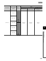
Term
Description
Base unit type
Generic term for the main base unit, extension base unit, slim type main base unit, redundant
Base unit
power main base unit, redundant power extension base unit, redundant type extension base
unit base unit, and multiple CPU high speed main base unit
Main base unit
Extension base unit
Generic term for the Q3B, Q3SB, Q3RB, and Q3DB
Generic term for the Q5B, Q6B, Q6RB, Q6WRB, QA1S5B, QA1S6B, QA6B,
and QA6ADP+A5B/A6B
Slim type main base unit
Another term for the Q3SB
Redundant power main base unit
Another term for the Q3RB
Redundant power extension base unit
Another term for the Q6RB
Redundant type extension base unit
Another term for the Q6WRB
Multiple CPU high speed main base
unit
Redundant base unit
Redundant power supply base unit
Another term for the Q3DB
Generic term for the redundant power main base unit, redundant power
extension base unit, and redundant type extension base unit
Generic term for the redundant power main base unit and redundant power extension base unit
Base unit model
Q3B
Generic term for the Q33B, Q35B, Q38B, and Q312B main base units
Q3SB
Generic term for the Q32SB, Q33SB, and Q35SB slim type main base units
Q3RB
Another term for the Q38RB main base unit for redundant power supply system
Q3DB
Generic term for the Q35DB, Q38DB and Q312DB multiple CPU high speed main base units
Q5B
Generic term for the Q52B and Q55B extension base units
Q6B
Generic term for the Q63B, Q65B, Q68B, and Q612B extension base units
Q6RB
Another term for the Q68RB extension base unit for redundant power supply system
Q6WRB
Another term for Q65WRB extension base unit for redundant system
QA1S5B
Another term for the QA1S51B extension base unit
QA1S6B
Generic term for the QA1S65B and QA1S68B extension base units
QA6B
Generic term for the QA65B and QA68B extension base units
A5B
Generic term for the A52B, A55B, and A58B extension base units
A6B
Generic term for the A62B, A65B, and A68B extension base units
QA6ADP+A5B/A6B
Abbreviation for A large type extension base unit where the QA6ADP is mounted
Power supply module
Generic term for the Q series power supply module, AnS series power supply module, A series
Power supply module
power supply module, slim type power supply module, redundant power supply module, and life
detection power supply module
Q series power supply module
AnS series power supply module
A series power supply module
Generic term for the Q61P-A1, Q61P-A2, Q61P, Q61P-D, Q62P, Q63P, Q64P, and Q64PN
power supply modules
Generic term for the A1S61PN, A1S62PN, and A1S63P power supply modules
Generic term for the A61P, A61PN, A62P, A63P, A68P, A61PEU, and A62PEU power supply
modules
Slim type power supply module
Abbreviation for the Q61SP slim type power supply module
Redundant power supply module
Generic term for the Q63RP and Q64RP redundant power supply modules
Life detection power supply module
Abbreviation for the Q61P-D life detection power supply module]
20
Term
Description
Network module
CC-Link IE module
MELSECNET/H module
Generic term for the CC-Link IE Controller Network module and the CC-Link IE Field Network
module
Abbreviation for the MELSECNET/H network module
Ethernet module
Abbreviation for the Ethernet interface module
CC-Link module
Abbreviation for the CC-Link system master/local module
Network
CC-Link IE
Generic term for the CC-Link IE Controller Network and the CC-Link IE Field Network
MELSECNET/H
Abbreviation for the MELSECNET/H network system
Memory extension
Memory card
SRAM card
Generic term for the SRAM card, Flash card, and ATA cards
Generic term for the Q2MEM-1MBS, Q2MEM-2MBS, Q3MEM-4MBS, and Q3MEM-8MBS
SRAM cards
Flash card
Generic term for the Q2MEM-2MBF and Q2MEM-4MBF Flash cards
ATA card
Generic term for the Q2MEM-8MBA, Q2MEM-16MBA, and Q2MEM-32MBA ATA cards
Generic term for the L1MEM-2GBSD and L1MEM-4GBSD SD memory cards
SD memory card
A memory device which consists of flash memory (abbreviation for Secure Digital Memory
Card)
Extended SRAM cassette
Generic term for the Q4MCA-1MBS, Q4MCA-2MBS, Q4MCA-4MBS, and Q4MCA-8MBS
extended SRAM cassette
Software package
Programming tool
GX Works2
GX Developer
PX Developer
Generic term for GX Works2 and GX Developer
Product name for the MELSEC programmable controller software package
Product name for SWD5C-FBDQ process control FBD software package
Others
A CPU module which controls each I/O module and intelligent function module
Control CPU
In a multiple CPU system, the CPU module which executes the control can be set for each
module.
Controlled module
I/O modules and intelligent function modules which are controlled by a control CPU
Abbreviation for the MELSEC communication protocol. The MELSEC communication protocol
MC protocol
is a communication method to access from an external device to the CPU module according to
the communication procedure for the Q series programmable controller (such as a serial
communication module, Ethernet module).
QA6ADP
Abbreviation for the QA6ADP QA conversion adapter module
Extension cable
Generic term for the QC05B, QC06B, QC12B, QC30B, QC50B, and QC100B extension cables
Tracking cable
Generic term for the QC10TR and QC30TR tracking cables for the Redundant CPU
Battery
GOT
Generic term for the Q6BAT, Q7BAT, and Q8BAT CPU module batteries, Q2MEM-BAT SRAM
card battery, and Q3MEM-BAT SRAM card battery
Generic term for Mitsubishi Graphic Operation Terminal, GOT-A*** series, GOT-F***
series, and GOT1000 series
21
PACKING LIST
The following items are included in the package of this product. Before use, check that all the items are included.
(1) CPU module
(a) Q00JCPU or Q00UJCPU
Product Name
Quantity
Module
1
Battery (Q6BAT)
1
Base unit mounting screw (M4 × 14 screw)
4
Safety Guidelines (IB-0800423)
1
(b) Other than Q00JCPU and Q00UJCPU
Product Name
Quantity
Module
1
Battery (Q6BAT)
1
(2) Main base unit
Product Name
Unit
1
Base unit mounting screw (M4 × 14 screw*1)
Safety Guidelines (IB-0800423)
*1
*2
Quantity
4/5*2
1
For the slim type main base unit, M4 × 12 screws are supplied.
Screws as many as the number of mounting holes are supplied.
(3) Extension base unite
Product Name
Unit
1
Base unit mounting screw (M4 × 14 screw)
*3
Quantity
4/5*3
Screws as many as the number of mounting holes are supplied.
(4) Power supply module or I/O module
Product Name
Module
22
Quantity
1
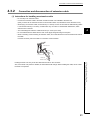
CHAPTER 1 OVERVIEW
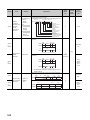
CHAPTER 1
1.1
OVERVIEW
1
Features
This section describes the features of Q series CPU modules.
(1) Large number of I/O points
The Q Series CPU module supports the following number of actual I/O points accessible to the I/O modules
mounted on the base unit.
(a) Basic model QCPU
• Q00JCPU:
256 points (X/Y0 to FF)
• Q00CPU, Q01CPU:
1024 points (X/Y0 to 3FF)
Up to 2048 points (X/Y0 to 7FF) are supported as the number of I/O device points usable for refreshing the
remote I/O of the CC-Link and link I/O (LX, LY) of the MELSECNET/H.
(b) High Performance model QCPU
One module can support 4096 points (X/Y0 to FFF).
Up to 8192 points (X/Y0 to 1FFF) are supported as the number of I/O device points usable for the remote I/O
stations in the MELSECNET/H remote I/O network, the CC-Link data link, and the MELSECNET/MINI-S3 data
link.
(c) Process CPU and Redundant CPU
Up to 8192 points (X/Y0 to 1FFF) are supported as the number of I/O device points usable for the remote I/O
stations in the MELSECNET/H remote I/O network and CC-Link data link.
(d) Universal model QCPU
• Q00UJCPU:
256 points (X/Y0 to FF)
• Q00UCPU, Q01UCPU:
1024 points (X/Y0 to 3FF)
• Q02UCPU:
• Q03UD(E)CPU, Q03UDVCPU,
2048 points (X/Y0 to 7FF)
Q04UD(E)HCPU, Q04UDVCPU,
Q06UD(E)HCPU, Q06UDVCPU,
Q10UD(E)HCPU, Q13UD(E)HCPU,
Q13UDVCPU, Q20UD(E)HCPU,
Q26UD(E)HCPU, Q26UDVCPU,
Q50UDEHCPU, Q100UDEHCPU:
4096 points (X/Y0 to FFF)
Up to 8192 points (X/Y0 to 1FFF) are supported as the number of I/O device points usable for the remote I/O
stations in the MELSECNET/H remote I/O network and CC-Link data link.
23
1.1 Features
One module can support 4096 points (X/Y0 to FFF).
(2) Large selection of CPU modules
The following lists the lineup of CPU available for various program size.
CPU module type
Basic model QCPU
High Performance model QCPU
Process CPU
Redundant CPU
Universal model QCPU
24
Program size
Q00(J)CPU
8K steps
Q01CPU
14Ksteps
Q02(H)CPU
28K steps
Q06HCPU
60K steps
Q12HCPU
124K steps
Q25HCPU
252K steps
Q02PHCPU
28K steps
Q06PHCPU
60K steps
Q12PHCPU
124K steps
Q25PHCPU
252K steps
Q12PRHCPU
124K steps
Q25PRHCPU
252K steps
Q00U(J)CPU
10K steps
Q01UCPU
15K steps
Q02UCPU
20K steps
Q03UD(E)CPU
30K steps
Q03UDVCPU
30K steps
Q04UD(E)HCPU
40K steps
Q04UDVCPU
40K steps
Q06UD(E)HCPU
60K steps
Q06UDVCPU
60K steps
Q10UD(E)HCPU
100K steps
Q13UD(E)HCPU
130K steps
Q13UDVCPU
130K steps
Q20UD(E)HCPU
200K steps
Q26UD(E)HCPU
260K steps
Q26UDVCPU
260K steps
Q50UDEHCPU
500K steps
Q100UDEHCPU
1000K steps
CHAPTER 1 OVERVIEW
1
(3) High-speed processing
High speed processing has been achieved.
CPU module type
Basic model QCPU
High Performance model QCPU
LD instruction processing speed
Q00JCPU
200ns
Q00CPU
160ns
Q01CPU
100ns
Q02CPU
79ns
Q02HCPU, Q06HCPU, Q12HCPU,
Q25HCPU
Q02PHCPU, Q06PHCPU, Q12PHCPU,
Process CPU
34ns
Q25PHCPU
Redundant CPU
Universal model QCPU
Q12PRHCPU, Q25PRHCPU
Q00UJCPU
120ns
Q00UCPU
80ns
Q01UCPU
60ns
Q02UCPU
40ns
Q03UD(E)CPU
20ns
Q04UD(E)HCPU, Q06UD(E)HCPU,
Q10UD(E)HCPU, Q13UD(E)HCPU,
Q20UD(E)HCPU, Q26UD(E)HCPU,
9.5ns
Q50UDEHCPU, Q100UDEHCPU
High-speed
Q03UDVCPU, Q04UDVCPU,
Universal model
Q06UDVCPU, Q13UDVCPU,
QCPU
Q26UDVCPU
1.9ns
(a) Basic model QCPU
MELSECNET/H link refreshing: 2.2ms/2K words*1
*1
The Q01CPU is used without using SB and SW, and the MELSECNET/H network module is mounted on the main base
unit.
(b) High Performance model QCPU, Process CPU, Redundant CPU or
Universal model QCPU
Access to the intelligent function module: 20µs/word (approximately 7 times*2)
MELSECNET/H link refreshing: 4.6ms/8K words (approximately 4.3 times*2)
*2
These are the values resulted from the following comparison:
• Comparing Q02HCPU with Q2ASHCPU-S1
• Comparing Q25PHCPU with Q4ARCPU
• Comparing Q25PRHCPU with Q4ARCPU
25
1.1 Features
The MELSEC Q series base unit high-speed system bus has achieved faster access to an intelligent function
module and link refresh with a network module.
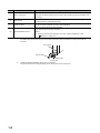
(4) Increase in debugging efficiency through high-speed communication with a
programming tool
High-speed communications at 115.2Kbps maximum are available by using RS-232 which reducing the time
required for writing and reading of programs and monitoring. Also, the communication time efficiency of
debugging has been increased.
In addition, High Performance model QCPUs (except for the Q02CPU), Process CPUs, Redundant CPUs and
Universal model QCPUs support USB, so that high-speed communications of 12Mbps are available.
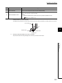
Q25HCPU(USB)
Q25HCPU(RS-232)
12
30
Q2ASHCPU
A2USHCPU-S1
86
94
0 10 20 30 40 50 60 70 80 90 100 (Unit:s)
(5) Use of AnS/A series I/O modules and special function modules
The AnS/A series compatible extension base units (QA1S5B, QA1S6B, QA6B, and
QA6ADP+A5B/A6B) can be connected to the main base unit where the High Performance model QCPU or
Universal model QCPU*1 is mounted. This enables the use of AnS/A series I/O modules and special function
modules.
*1
The Universal model QCPU whose serial number (first five digits) is "13102" or later is applicable.
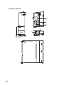
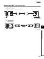
(6) Miniaturized modules (space-saving size)
5 Slot Main Base Unit 245mm(9.65inch)
8 Slot Main Base Unit 328mm(12.92inch)
12 Slot Main Base Unit 439mm(17.28inch)
26
(depth:98mm(3.86inch))
AnS series
Q series
98mm (3.86inch)
The installation space for the Q series has been reduced by approx. 60% compared with the AnS series.
CHAPTER 1 OVERVIEW
1
(7) Connection of up to 7 extension base units
Up to seven extension base units can be connected to the Q series CPU module.
The overall extension cable length is 13.2m (43.31feet), which allows flexible layout of base units.
(8) Memory extension
By extending the memory capacity of a CPU module, large size files can be managed. Comments can be set to
all data devices and old programs can be saved as correction history.
(a) Memory card
A memory card (maximum 32M bytes) can be installed. (The maximum size is available only for ATA cards.)
Memory cards are used for the following operations.
• Boot operation
• Restoring backup data
• Writing programs to the ROM
Data that cannot be stored in the built-in memory of the CPU module, such as sampling trace data and file
register data, can be stored as well.
(b) SD memory card
SD memory cards are used for the following operations.
• Boot operation
• Restoring backup data
• Data backup
• Data logging
An extended SRAM cassette extends the capacity of the standard RAM in a CPU module.
• An extended SRAM cassette can be used together with an SD memory card, allowing users to store data
separately (for example, boot data in an SD memory card and device data in an extended SRAM
cassette). This improves maintainability.
• With existing CPU modules, file register areas in the standard RAM and an SRAM card cannot be
accessed sequentially, and the boundary needs to be considered at programming. If the standard RAM
capacity is extended using an extended SRAM cassette, the device area can be extended without
considering the boundary.
Remark
Memory extension methods differ depending on the CPU module. (
Page 42, Section 2.2)
27
1.1 Features
(c) Extended SRAM cassette
(9) Automatic write to the standard ROM
Note 1.1,
Note 1.2
Note 1.1 Note 1.2
Parameters and programs in a memory card or SD memory card can be written to the standard ROM of the CPU
module without using a programming tool.
If the boot operation is being performed from the standard ROM, parameters and programs in a memory card or
SD memory card can be written to the standard ROM by inserting it to the CPU module. Users do not need a
programming tool (personal computer) on hand to modify parameters and programs.
(10)External input/output forced on/off
Note 1.1
Forced on and off of external input and output is available using a programming tool even when the CPU module
is running or program is being processed.
Also, wiring test and operation test can be conducted without halting the CPU module by forcibly turning on or off
the I/O.
(11)Remote password function
When the built-in Ethernet port QCPU, Ethernet module, or serial communication module is externally accessed,
an access to the CPU module can be controlled by setting a remote password.
(12)Remote I/O network of MELSECNET/H
Note 1.1
A MELSECNET/H remote I/O system can be configured by installing a MELSECNET/H remote master station.
● The remote password can be set up when the Ethernet module, or serial communication module of function version B or
later is used.
● The MELSECNET/H remote I/O network can be implemented when the MELSECNET/H network module of function
version B or later is used.
(13)Support of multiple CPU systems
CPU module supports the multiple CPU system.
Multiple CPU systems can be constructed in combination with CPU modules, motion CPU(s), PC CPU module(s),
and C Controller module.
For details of the multiple CPU system, refer to the following.
QCPU User's Manual (Multiple CPU System)
Note 1.1
Basic
The Basic model QCPU does not support the following functions.
• Automatic write to the standard ROM
• External input/output forced on/off
• MELSECNET/H remote I/O network
Note 1.2
Universal
The Universal model QCPU does not support the following function.
• Parameter setting of automatic write to the standard ROM
28
CHAPTER 1 OVERVIEW
1
(14)Support of redundant power supply systems
The redundant power supply system can be configured using a redundant base unit and redundant power supply
modules.
The system can continue operation even if one of the power supply modules fails, since the other will supply the
power.
(15)Direct connection to Ethernet
Note 1.3
Note 1.3
The Built-in Ethernet port QCPU module allows direct connections to Ethernet.
For details of the functions, refer to the following.
QnUCPU User's Manual (Communication via Built-in Ethernet Port)
1.1 Features
Note 1.3
Universal
Only the Built-in Ethernet port QCPU supports this function.
29
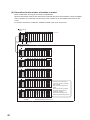
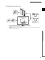
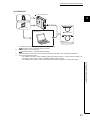
CHAPTER 2
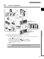
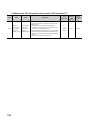
SYSTEM CONFIGURATION
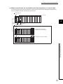
This chapter describes system configurations, precautions, and components of the Q Series CPU module.
This section describes system configurations for a single CPU system with the Basic model QCPU, High Performance
model QCPU, Process CPU, or Universal model QCPU, and a system configuration when using GOT by bus
connection.
For a multiple CPU system and redundant system (when using the Redundant CPU), refer to the following.
QCPU User's Manual (Multiple CPU System)
QnPRHCPU User's Manual (Redundant System)
30
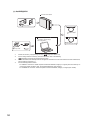
CHAPTER 2 SYSTEM CONFIGURATION
2.1
Overall Configuration
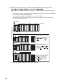
2
Extended SRAM cassette
Memory card, SD memory card
Basic model QCPU
High Performance model QCPU
Process CPU
Universal model QCPU
Battery for QCPU (Q6BAT)
Q7BAT-SET
Q3
Q3
Q3
Q3
Battery holder
B main base unit
RB redundant power main base unit
SB slim type main base unit
DB multiple CPU high speed main base unit
Battery for QCPU (Q7BAT)
Q8BAT-SET
Extension cable
Battery for QCPU (Q8BAT)
Q5 B extension base unit
Q6 B extension base unit
Q6 RB redundant power extension base unit
QA1S5 B extension base unit
QA1S6 B extension base unit
QA6 B extension base unit
2.1 Overall Configuration
Q8BAT connection cable
Power supply module/I/O module/Intelligent function module/Special function module
The combination of modules depends on the devices used in the configuration.
For the applicable combinations, refer to the following.
• CPU modules and base units, batteries, memory cards, SD memory cards, and/or extended SRAM
cassettes (
Page 32, Section 2.2)
• Base units and power supply modules (
• Main base units and extension base units (
Page 216, CHAPTER 7)
Page 251, CHAPTER 8)
• CPU modules and intelligent function modules or special function modules
(
User's manual for each module)
To correctly configure a system, observe precautions described in Page 35, Section 2.3.
31
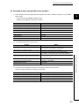
2.2
Component List
(1) Basic model QCPU
Item
Description
Main base unit
Q33B, Q35B, Q38B, Q312B
Applicable main base
Redundant power main base unit
Q38RB
unit*1
Slim type main base unit
Q32SB, Q33SB, Q35SB
Multiple CPU high speed main base unit
Q35DB, Q38DB, Q312DB
Model requiring no power supply module
Q52B, Q55B
Model requiring a Q series power supply module
Q63B, Q65B, Q68B, Q612B
Redundant power extension base unit
Q68RB
Applicable extension base
unit
Maximum number of
connectable extension
base units
Q00JCPU: 2
Q00CPU, Q01CPU: 4
Maximum number of
Q00JCPU: 16 (max. 16 slots)
mountable modules
Q00CPU, Q01CPU: 24 (max. 24 slots)
Extension cable
QC05B, QC06B, QC12B, QC30B, QC50B, QC100B
Total length of extension
cables
13.2m (43.31 feet)
Memory extension
----
Applicable battery
Q6BAT
*1
32
The Q00JCPU does not require a power supply module and the main base unit since the module is an integrated
combination of a power supply module and the main base unit.
CHAPTER 2 SYSTEM CONFIGURATION
(2) High Performance model QCPU
Item
Description
Applicable main base unit
Applicable extension base
unit
Main base unit
Q33B, Q35B, Q38B, Q312B
Redundant power main base unit
Q38RB
Slim type main base unit
Q32SB, Q33SB, Q35SB
Multiple CPU high speed main base unit
Q35DB, Q38DB, Q312DB
Model requiring no power supply module
Q52B, Q55B
Model requiring a Q series power supply module
Q63B, Q65B, Q68B, Q612B
Redundant power extension base unit
Q68RB
Model requiring no AnS series power supply
2
QA1S51B
module*1
Model requiring a AnS series power supply module*1
QA1S65B, QA1S68B
Model requiring A series power supply module*1
QA65B, QA68B, QA6ADP+A6B
Model requiring no A series power supply module*1
QA6ADP+A5B
Maximum number of
connectable extension
7
base units
Maximum number of
64 (max. 64 slots)
mountable modules
Extension cable
QC05B, QC06B, QC12B, QC30B, QC50B, QC100B
Total length of extension
13.2m (43.31 feet)
cables
Memory extension
Q2MEM-1MBS, Q2MEM-2MBS
Flash card
Q2MEM-2MBF, Q2MEM-4MBF
ATA card
Q2MEM-8MBA, Q2MEM-16MBA, Q2MEM-32MBA
Applicable battery
*1
Q6BAT, Q7BAT, Q8BAT
The A/AnS series extension base units are applicable only when the Q3B is used as a main base unit.
(3) Process CPU
Item
Applicable main base unit
Applicable extension base
unit
Description
Main base unit
Q33B, Q35B, Q38B, Q312B
Redundant power main base unit
Q38RB
Multiple CPU high speed main base unit
Q35DB, Q38DB, Q312DB
Model requiring no power supply module
Q52B, Q55B
Model requiring a Q-series power supply module
Q63B, Q65B, Q68B, Q612B
Redundant power extension base unit
Q68RB
Maximum number of
connectable extension
7
base units
Maximum number of
64 (max. 64 slots)
mountable modules
Extension cable
QC05B, QC06B, QC12B, QC30B, QC50B, QC100B
Total length of extension
13.2m (43.31 feet)
cables
Memory extension
SRAM card
Q2MEM-1MBS, Q2MEM-2MBS
Flash card
Q2MEM-2MBF, Q2MEM-4MBF
ATA card
Applicable battery
Q2MEM-8MBA, Q2MEM-16MBA, Q2MEM-32MBA
Q6BAT, Q7BAT, Q8BAT
33
2.2 Component List
SRAM card
(4) Universal model QCPU
Item
Description
Main base unit
Q33B, Q35B, Q38B, Q312B
Applicable main base
Redundant power main base unit
Q38RB
unit*1
slim type main base unit
Q32SB, Q33SB, Q35SB
Multiple CPU high speed main base unit
Q35DB, Q38DB, Q312DB
Model requiring no power supply module
Q52B, Q55B
Model requiring a Q-series power supply module
Q63B, Q65B, Q68B, Q612B
Redundant power extension base unit
Q68RB
Model requiring no AnS series power supply
Applicable extension base
unit
QA1S51B
module*3
Model requiring an AnS series power supply
QA1S65B, QA1S68B
module*3
Model requiring no A series power supply module*3
QA65B, QA68B, QA6ADP+A6B
Model requiring an A series power supply module*3
QA6ADP+A5B
Maximum number of
Q00UJCPU: 2
connectable extension
Q00UCPU, Q01UCPU, Q02UCPU: 4
base units
Other than above: 7
Q00UJCPU: 16 (max. 16 slots)
Maximum number of
Q00UCPU, Q01UCPU: 24 (max. 24 slots)
mountable modules
Q02UCPU: 36 (max. 36 slots)
Other than above: 64 (max. 64 slots)
Extension cable
QC05B, QC06B, QC12B, QC30B, QC50B, QC100B
Total length of extension
13.2m (43.31 feet)
cables
Other than
QnUDVCPU
Memory
*2
extension
Applicable battery
*1
*2
*3
Q2MEM-1MBS, Q2MEM-2MBS, Q3MEM-4MBS,
Q3MEM-8MBS
Flash card
Q2MEM-2MBF, Q2MEM-4MBF
ATA card
Q2MEM-8MBA, Q2MEM-16MBA, Q2MEM-32MBA
SD memory card
QnUDVCPU
34
SRAM card
Extended SRAM cassette
L1MEM-2GBSD, L1MEM-4GBSD
Q4MCA-1MBS, Q4MCA-2MBS, Q4MCA-4MBS,
Q4MCA-8MBS
Q6BAT, Q7BAT, Q8BAT
The Q00JCPU does not require a power supply module and the main base unit since the module is an integrated
combination of a power supply module and the main base unit.
Memory cards cannot be used in the Q00U(J)CPU and Q01UCPU.
The A/AnS series extension base units can be used when the following conditions are satisfied.
• The serial number (first five digits) of the Universal model QCPU used is "13102" or later.
• The Q3B or Q3DB is used as a main base unit, or the Q00UJCPU is used.
CHAPTER 2 SYSTEM CONFIGURATION
2.3
Precautions for System Configuration
This section describes restrictions on the system configuration using the Q series CPU module.
2
(1) Number of mountable modules
The number of mountable modules and supported functions are restricted depending on the module type.
(a) When the Basic model QCPU is used
Product
CC-Link IE Controller Network module
Model
Maximum number of modules/units
per system
• QJ71GP21-SX
• QJ71GP21S-SX
• QJ71LP21
• QJ71BR11
• QJ71LP21-25
MELSECNET/H module
Only 1 module*1
• QJ71LP21S-25
• QJ71LP21G
• QJ71LP21GE
• QJ71NT11B
• QJ71E71
Ethernet module
• QJ71E71-B2
• QJ71E71-B5
Only 1 module
• QJ71E71-100
CC-Link module
• QJ61BT11
• QJ61BT11N
Up to 2 modules*2
2.3 Precautions for System Configuration
• QI60*1
• QX40H*6
Interrupt module
• QX70H*6
•
Only 1 module*3
QX80H*6
• QX90H*6
High speed data logger module
• QD81DL96
Only 1 module*5
• GOT-A900 Series (for bus
GOT
connection only)*4
• GOT1000 Series (for bus
Up to 5 units
connection only)*4
*1
*2
*3
*4
The number is a total of the CC-Link IE Controller Network module and MELSECNET/H module.
Modules of function version B or later are available.
The number is for interrupt modules with no interrupt pointer setting.
With interrupt pointer setting, there is no restriction on the number of modules.
For interrupt pointer setting, refer to the following.
Qn(H)/QnPH/QnPRHCPU User's Manual (Function Explanation, Program Fundamentals)
For the available GOT models, refer to the following.
GOT-A900 Series User's Manual (GT Work2 Version2/GT Designer2 Version2 Compatible Connection System
Manual)
*5
*6
GOT1000 Series Connection Manual
One module can be mounted for one control CPU.
The module is available only when the interrupt module is selected by setting the function selector switch (SW2) to OFF.
35
(b) When the High Performance model QCPU or Process CPU is used
Product
Model
CC-Link IE Controller Network
• QJ71GP21-SX
module*1
• QJ71GP21S-SX
Maximum number of
modules/units per system
Up to 2 modules
• QJ71LP21
• QJ71BR11
Up to 4 modules
• QJ71LP21-25
MELSECNET/H module
• QJ71LP21S-25
Up to 4 modules
in total
• QJ71LP21G
• QJ71LP21GE
• QJ71NT11B
• QJ71E71
Ethernet module
• QJ71E71-B2
• QJ71E71-B5
Up to 4 modules
• QJ71E71-100
CC-Link module
• QJ61BT11
• QJ61BT11N
No restriction*2
MELSECNET/MINI-S3 data
• A1SJ71PT32-S3
No restriction
link module*3
• A1SJ71T32-S3
(Auto refresh setting not allowed)
• A1SD51S
• A1SD21-S1
AnS Series special function
• A1SJ71J92-S3(When using GET/PUT service)
module*3
• A1SJ71AP23Q
Up to 6 modules in total
• A1SJ71AR23Q
• A1SJ71AT23BQ
• A1SI61*3
• QI60
Interrupt module
• QX40H*5
• QX70H*5
Only 1 module
• QX80H*5
• QX90H*5
High speed data logger module
GOT
*1
*2
*3
*4
• QD81DL96
• GOT-A900 Series (only for bus connection)*4
• GOT100 0Series (only for bus connection)*4
Only 1 module*6
Up to 5 units
Only the High Performance model QCPU whose serial number (first five digits) is "09012" or later and Process CPU
whose serial number (first five digits) is "10042" or later can be used.
One CPU module can control the following number of modules by setting CC-Link network parameters in GX Developer.
• The serial number (first five digits) of the CPU module is "08031" or earlier: up to 4 modules
• The serial number (first five digits) of the CPU module is "08032" or later: up to 8 modules
There is no restriction on the number of modules when the parameters are set with the CC-Link dedicated instructions.
For the CC-Link system master/local modules whose parameters can be set by the dedicated instructions, refer to the
following.
MELSEC-Q CC-Link System Master/Local Module User's Manual
The module is available only when the High Performance model QCPU is used.
For the available GOT models, refer to the following.
GOT-A900 Series User's Manual (GT Work2 Version2/GT Designer2 Version2 Version2 Compatible Connection
System Manual)
*5
*6
36
GOT1000 Series Connection Manual
The module is available only when the interrupt module is selected by setting the function selector switch (SW2) to OFF.
One module can be mounted for one control CPU.
CHAPTER 2 SYSTEM CONFIGURATION
(c) When the Redundant CPU is used
For the modules with restriction on the number of mountable modules, refer to the following.
QnPRHCPU User's Manual (Redundant System)
2
(d) When the Universal model QCPU is used
Product
Model
CC-Link IE Controller Network
• QJ71GP21-SX
module*1
• QJ71GP21S-SX
Maximum number of
modules/units per system
• QJ71LP21
• QJ71BR11
• QJ71LP21-25
MELSECNET/H module
Up to 4 modules*2*3
• QJ71LP21S-25
• QJ71LP21G
• QJ71LP21GE
• QJ71NT11B
CC-Link IE Field network module
• QJ71GF11-T2
No restriction*8
• QJ71E71
Ethernet module
• QJ71E71-B2
• QJ71E71-B5
Up to 4 modules*3
• QJ71E71-100
CC-Link module
MELSECNET/MINI-S3 data link
module
*11
• QJ61BT11
• QJ61BT11N
No restriction*4*5
• A1SJ71PT32-S3
No restriction
• A1SJ71T32-S3
(Auto refresh setting not allowed)
2.3 Precautions for System Configuration
• A1SD51S
• A1SD21-S1
• A1SJ71J92-S3
AnS series special function module*11
(When using GET/PUT service)
Up to 6 modules in total
• A1SJ71AP23Q
• A1SJ71AR23Q
• A1SJ71AT23BQ
• A1SI61*11
• QX40H*10
Interrupt module
• QX70H*10
Only 1 module*6
• QX80H*10
• QX90H*10
High speed data logger module*12
GOT
*1
*2
*3
*4
• QD81DL96
• GOT1000 Series (only for bus
connection)*7
Only 1 module*9
Up to 5 units
Only the CC-Link IE Controller Network module whose serial number (first five digits) is "09042" or later can be used.
The number is a total of the CC-Link IE Controller Network modules and MELSECNET/H network modules.
The number of mountable modules for the Q00UJCPU, Q00UCPU, and Q01UCPU is only one module, and two
modules for the Q02UCPU.
Modules of function version B or later are available.
37
*5
*6
*7
*8
*9
*10
*11
*12
38
One CPU module can control the following number of modules by setting CC-Link network parameters in a programming
tool.
• Q00UJCPU, Q00UCPU, Q01UCPU: up to 2 modules
• Q02UCPU: up to 4 modules
• Q03UD(E)CPU, Q03UDVCPU, Q04UD(E)HCPU, Q04UDVCPU, Q06UD(E)HCPU, Q06UDVCPU, Q10UD(E)HCPU,
Q13UD(E)HCPU, Q13UDVCPU, Q20UD(E)HCPU, Q26UD(E)HCPU, Q26UDVCPU, Q50UDEHCPU,
Q100UDEHCPU: up to 8 modules
There is no restriction on the number of modules when the parameters are set with the CC-Link dedicated instructions.
For the CC-Link system master/local modules whose parameters can be set with the dedicated instructions, refer to the
following.
CC-Link System Master/Local Module User's Manual
The number is for interrupt modules with no interrupt pointer setting.
With interrupt pointer setting, there is no restriction on the number of modules.
For interrupt pointer setting, refer to the following.
QnUCPU User's Manual (Function Explanation, Program Fundamentals)
For the available GOT models, refer to the following.
GOT1000 Series Connection Manual
One CPU module can control the following number of modules by setting CC-Link network parameters in a programming
tool.
• Q00UJCPU, Q00UCPU, Q01UCPU: up to 2 modules
• Q02UCPU: up to 4 modules
• Q03UD(E)CPU, Q03UDVCPU, Q04UD(E)HCPU, Q04UDVCPU, Q06UD(E)HCPU, Q06UDVCPU, Q10UD(E)HCPU,
Q13UD(E)HCPU, Q13UDVCPU, Q20UD(E)HCPU, Q26UD(E)HCPU, Q26UDVCPU, Q50UDEHCPU,
Q100UDEHCPU: up to 8 modules
There is no restriction on the number of modules when the parameters are set with the CC-Link IE Field Network
dedicated instructions.
For the CC-Link IE Field Network modules whose parameters can be set with the dedicated instructions, refer to the
following.
MELSEC-Q CC-Link IE Field Network Master/Local Module User's Manual
One module can be mounted for one control CPU.
The module is available only when the interrupt module is selected by setting the function selector switch (SW2) to OFF.
This module is applicable only when the Universal model QCPU whose serial number (first five digits) is "13102" or later
is used.
The High-speed Universal model QCPU supports only the high speed data logger module whose serial number (first five
digits) is "14122" or later.
CHAPTER 2 SYSTEM CONFIGURATION
(2) Modules with limitations when using a Built-in Ethernet port QCPU
The following table lists restrictions on modules when Built-in Ethernet port QCPU is used.
Product
Model
Serial number (first five digits)
2
QJ71LP21-25
QJ71LP21S-25
MELSECNET/H module
Some modules have restrictions depending
QJ71LP21G
on the use conditions.*1
QJ71LP21GE
QJ71BR11
QJ71C24N
Serial communication module
QJ71C24N-R2
"10042" or later
QJ71C24N-R4
Web server module
QJ71WS96
MES interface module
QJ71MES96
*1
"10012" or later
("14122" or later when used with the
QnUDVCPU)
If the MELSECNET module meets the following all conditions, use the MELSECNET/H module whose serial number
(first five digits) is "10042" or later.
1) A multiple CPU system containing a Built-in Ethernet port QCPU is configured.
2) To an Ethernet port of a Built-in Ethernet port QCPU, a programming tool or GOT is connected.
3) From a programming tool or GOT, access is made to another station through a MELSECNET/H module controlled
by another CPU.
4) The access target on another station is an A/QnA series CPU module.
(3) Number of available slots
Empty slots are included in the number of available slots (modules) in the base unit.
The number of available slots (modules) varies depending on the base unit.
Page 217, CHAPTER 8
For the assignment concepts of base units and I/O numbers, refer to the following.
User's manual for the CPU module used (Function Explanation, Program Fundamentals)
CPU
0
1
2
3
4
Input Input Empty Input Output
Number of
slot points
16
16
0
16
16
points points point points points
Occupies 1 slot.
39
2.3 Precautions for System Configuration
(One slot is occupied even when "empty" and "0 points" are set for the slot 2 as shown in the following figure.)
(4) Precautions for the number of modules to mount
Mount modules within the range of the number of available slots.
When the total number of slots for the main base unit and extension base units exceeds the number of available
slots (for example, six 12-slot base units are used), mount modules only on the available slots so that no error
occurs.
If a module is mounted on a invalid slot, "SP.UNIT LAY ERR." (error code: 2124) occurs.
Main base unit
Q312B
CPU
Power supply
module
0
1
2
3
4
5
6
7
8
9
10
11
Slot number
CPU module
Extension base unit
Q612B
12
13
14
15
16
17
18
19
20
21
22
23
Extension 1
24
25
26
27
28
29
30
31
32
33
34
35
Extension 2
36
37
38
39
40
41
42
43
44
45
46
47
Extension 3
48
49
50
51
52
53
54
55
56
57
58
59
Extension 4
Q612B
Q612B
Q612B
Q612B
Extension 5
Modules can be
installed.
40
Prohibit
Prohibit
Prohibit
Prohibit
Prohibit
63
Prohibit
62
Prohibit
61
Prohibit
60
When the GOT has been busconnected, one slot of extension
base 1 is used.
Also one GOT occupies 16 I/O
points.
When using the GOT, consider
the number of slots and the
number of I/O points.
Refer to the GOT Manual for
details of busconnecting the GOT.
Modules cannot be installed.
(Installing modules will result in error.)
CHAPTER 2 SYSTEM CONFIGURATION
(5) Precautions when using AnS/A series modules
1) When using the AnS series special function modules shown below, a limitation is placed on an accessible
device range.
• A1SJ71J92-S3 type JEMANET interface module
2
• A1SD51S type intelligent communication module
Device
Accessible device range
Input (X), Output (Y)
X/Y0 to 7FF
Internal relay (M), Latch relay (L)
M/L0 to 8191
Link relay (B)
B0 to FFF
Timer (T)
T0 to 2047
Counter (C)
C0 to 1023
Data register (D)
D0 to 6143
Link register (W)
W0 to FFF
Annumciator (F)
F0 to 2047
2) The modules listed below cannot be used.
Product
MELSECNET/10 network module
MELSECNET(II), /B data link module
Model
A1SJ71LP21, A1SJ71BR11, A1SJ71LR21, A1SJ71QLP21,
A1SJ71QLP21S, A1SJ71QBR11, A1SJ71QLR21
A1SJ71AP21, A1SJ71AR21, A1SJ71AT21B
A1SJ71E71N-T, A1SJ71E71N3-T, A1SJ71E71N-B2(-B5),
Ethernet module
A1SJ71QE71N-T, A1SJ71QE71N3-T, A1SJ71QE71N-B2(-B5)
A1SJ71UC24-R2(-PRF), A1SJ71QC24(-R2), A1SJ71QC24N(-R2),
A1SJ71QC24N1(-R2)
Computer link/multidrop link module
A1SJ71UC24-R4*1
CC-Link system master/local module
A1SJ61BT11, A1SJ61QBT11
ME-NET interface module
A1SJ71ME81
*1
Only multidrop link function can be used. The computer link function and printer function cannot be used.
3) The AnS/A series dedicated instructions for the following modules cannot be used.
Rewriting using the FROM or TO instruction is required.
Product
Model
High speed counter module
A1SD61, A1SD62, A1SD62D(-S1), A1SD62E
MELSECNET/MINI-S3
A1SJ71PT32-S3, A1SJ71T32-S3
Positioning module
A1SD75P1-S3(P2-S3/P3-S3)
ID module
A1SJ71ID1-R4, A1SJ71ID2-R4
41
2.3 Precautions for System Configuration
Serial communication module, computer link module
4) System configurations and functions are partially restricted when writing the parameters set under the "High
speed interrupt fixed scan interval" setting.
For the restrictions, refer to the following.
User's manual for the CPU module used (Function Explanation, Program Fundamentals)
5) For restrictions on mounting the A series module on the QA6B or QA6ADP+A5B/A6B, refer to the
following.
QA65B/QA68B Extension Base Unit User's Manual
QA6ADP QA Conversion Adapter Module User's Manual
6) For restrictions on using varying AnS/A series compatible extension base units, refer to Page 74, Section
4.3.
42
CHAPTER 2 SYSTEM CONFIGURATION
2.3.1
Bus connection of GOT
In the system with the Q series CPU module, the GOT can be connected on the bus using the extension cable
2
connector of the main base unit or extension base unit.
This section describes the system configuration of a GOT on the bus.
For details of bus connection of the GOT, refer to the following.
GOT-A900 Series User's Manual (Connection)
GOT1000 Series Connection Manual
(1) GOT recognized by CPU module
When a GOT is connected by bus, the CPU module recognizes the GOT as an intelligent function module with 16
I/O points.
Therefore, the I/O must be assigned to the CPU module in the GOT setup.
(When connecting a GOT on the bus, one extension base (16 points x 10 slots) must be occupied by the GOT.)
For details of the GOT setup, refer to the following.
GOT-A900 Series Operating Manual (Extension Function /Option Function)
GT15 User's Manual
GT16 User's Manual (Basic Utility)
(2) Maximum number of GOTs
Up to five GOTs can be connected on the bus.
2.3 Precautions for System Configuration
2.3.1 Bus connection of GOT
43
(3) Precautions
• When connecting a GOT on the bus, position the GOT in the base subsequent to base units. Do not position
the GOT between base units.
• Extension cables for connecting a GOT on the bus must be a maximum of 13.2m (43.31 feet) in total length.
• A bus extension connector box (A9GT-QCNB) is required when a first GOT connected on the bus is installed
13.2 m (43.31 feet) or more away from the main base unit. (Note that the bus extension connector box
cannot be used for the Q00JCPU.)
For details of the A9GT-QCNB, refer to the following.
A9GT-QCNB Type Bus Extension Connector Box User's Manual
• When using a redundant base unit (Q3RB/Q6RB/Q6WRB) as the base unit, a GOT cannot be
connected on the bus.)
• When using the QA1S6B as a extension base unit, install the GOT in the base subsequent to the
extension base units but assign the I/O number subsequent to Q6B/Q5B.
Extension
stage number I/O number
00 to 7F
Q38B main base unit
Q68B extension base unit
1
80 to FF
QA1S68B extension base unit
3
1A0 to 21F
GOT
2
100 to 19F
• When using the QA1S5B, QA6B, or QA6ADP+A5B/A6B as an extension base unit, the GOT cannot
be connected to the bus.
• Before starting up the CPU module, initialize the GOT (Set up the extension base and slot number in the
GOT setup.) that is to be connected to the bus.
• Apply the power to the CPU module and GOT by either of the following way.
1) Simultaneously turn on the CPU module and GOT.
2) Turn on the CPU module first, and then the GOT.
• For the applicable GOT, refer to Page 35, Section 2.3 (1).
• Ground the FG wire between the programmable controller and the GOT on the GOT side.
For installation, refer to the manual for the GOT used.
44
CHAPTER 2 SYSTEM CONFIGURATION
(4) Outline of system configuration
Main base unit ... The figure shows the configuration when 16-point modules are loaded to each slot.
2
Q series
power supply
module
0
1
2
3
4
.... Slot number
10 to 1F
20 to 2F
30 to 3F
40 to 4F
CPU
00 to 0F
Q35B (5 slots occupied)
.... I/O number
CPU module
Extension base unit ... The figure shows the configuration when 16-point modules are loaded to each slot.
12
B0 to BF
C0 to CF
90 to 9F
11
13
14
15
16
17
110 to 11F
10
80 to 8F
70 to 7F
9
100 to 10F
60 to 6F
8
F0 to FF
50 to 5F
7
E0 to EF
6
D0 to DF
5
A0 to AF
Q68B (8 slots occupied)
Q65B (5 slots occupied)
3)
No. of extension stages: 3
slots No.: 1
No. of extension stages: 3
slots No.: 2
4)
5)
No. of extension stages: 3
slots No.: 3
No. of extension stages: 3
slots No.: 4
Set on
the GOT
side.
18
19
20
21
22
130 to 13F
140 to 14F
150 to 15F
160 to 16F
Stage extension image for GOT connection viewed from CPU module
120 to 12F
No. of extension stages: 3
slots No.: 0
2)
2.3 Precautions for System Configuration
2.3.1 Bus connection of GOT
1)
1)
2)
3)
4)
23
24
25
26
27
GOT (No. of extension stages: 3)
16 points ×10 slots occupied
5)
Set to empty in "I/O assignment setting"
of PLC parameter
45
Note 2.1
• Q00JCPU and Q00UJCPU: 2
• When using Q00CPU, Q01CPU, Q00UCPU,
Q01UCPU, or Q02UCPU
Maximum number
:4
of connectable
• When using High Performance model QCPU, Process
extension base units
CPU, Q03UD(E)CPU, Q03UDVCPU,
(for GOT bus
Q04UD(E)HCPU, Q04UDVCPU, Q06UD(E)HCPU,
connection)
Q06UDVCPU, Q10UD(E)HCPU, Q13UD(E)HCPU,
The final level is for GOT only.
Q13UDVCPU, Q20UD(E)HCPU, Q26UD(E)HCPU,
Q26UDVCPU, Q50UDEHCPU, or Q100UDEHCPU
:7
• Q00JCPU or Q00UJCPU: 16 - (number of connected GOTs)
• When using Q00CPU, Q01CPU, Q00UCPU, or Q01UCPU
24 - (number of connected GOTs) module
Maximum number
• When using Q02UCPU
of mountable
36 - (number of connected GOTs) module
modules
• When using High Performance model QCPU, Process CPU, Q03UD(E)CPU, Q03UDVCPU, Q04UD(E)HCPU,
Q04UDVCPU, Q06UD(E)HCPU, Q06UDVCPU, Q10UD(E)HCPU, Q13UD(E)HCPU, Q13UDVCPU,
Q20UD(E)HCPU, Q26UD(E)HCPU, Q26UDVCPU, Q50UDEHCPU, or Q100UDEHCPU
64 - (number of connected GOTs) module
Applicable main
Q33B, Q35B, Q38B, Q312B, Q35DB, Q38DB, Q312DB
base unit
Model requiring no power supply module
Q52B, Q55B
Applicable
Model requiring a Q-series power supply module
Q63B, Q65B, Q68B, Q612B
extension base unit
Model requiring a AnS series power supply
module
Note 2.2
Applicable
QA1S65B, QA1S68B
QC05B, QC06B, QC12B, QC30B, QC50B, QC100B
extension cable
Q series power
supply module
Q61P-A1, Q61P-A2, Q61P, Q61P-D, Q62P, Q63P, Q64P, Q64PN
Note 2.1
AnS series power
supply module
A1S61PN, A1S62PN, A1S63P
Note 2.2
Note 2.2
Note 2.1
Basic
Universal
Since the Q00JCPU and Q00UJCPU are modules integrated with a power supply module and main base unit, the main
base unit (Q3B) and Q series power supply module are not required.
Note 2.2
High
performance
Universal
Only the High Performance model QCPU or the Universal model QCPU whose serial number (first five digits) is "13102"
or later supports the use of these extension base units.
46
CHAPTER 2 SYSTEM CONFIGURATION
2.3.2
Peripheral device configuration
This section describes peripheral devices that can be used in a system where the Basic model QCPU, High
2
Performance model QCPU, Process CPU, or Universal model QCPU is installed.
(1) When the Basic model QCPU is used
Basic model QCPU
Personal Computer (GX Works2, GX Developer, GX Configurator) *1
For the versions of GX Works2, GX Developer, and GX Configurator that can be used with the Basic model QCPU, refer
to Page 604, Appendix 5.1.
47
2.3 Precautions for System Configuration
2.3.2 Peripheral device configuration
*1
RS-232 cable
(2) When the High Performance model QCPU is used
High Performance model QCPU
Memory card
1
RS-232 cable
Personal Computer
(GX Works2, GX Developer, GX Configurator) * 4
USB cable
(Connector type B)
Memory card
1
2, 3
PC card
adapter
Programming unit, connection cable * 5 * 6
*1
*2
*3
*4
*5
*6
48
Format ATA cards by a programming tool only. (
Page 234, Section 9.3)
Not applicable to the Q02CPU.
For the writing method to a memory card and USB cables, refer to the following.
Operating manual for the programming tool used
For the GX Works2, GX Developer and GX Configurator versions that can be used with the High Performance model
QCPU, refer to Page 604, Appendix 5.1.
For inquiries and orders of a programming unit (EPU01) and connection cable (EPU20R2CBL), please contact your
local Mitsubishi Electric Engineering Co., Ltd. sales office.
Programming units cannot be used when the "High speed interrupt fixed scan interval" parameter is written to the High
Performance model QCPU whose serial number (first five digits) is “04012” or later.
CHAPTER 2 SYSTEM CONFIGURATION
(3) When the Process CPU is used
Process CPU
2
Memory card
1
Personal Computer
(GX Works2, GX Developer,
GX Configurator, PX Developer)
Memory card
1
RS-232 cable
3
PC card
adapter
USB cable
(Connector type B)
2
*1
*2
Format ATA cards by a programming tool only. (
Page 234, Section 9.3)
For the writing method to a memory card and USB cables, refer to the following.
*3
Operating manual for the programming tool used
For the GX Works2, GX Developer, GX Configurator, and PX Developer versions that can be used with the Process
CPU, refer to Page 604, Appendix 5.1.
2.3 Precautions for System Configuration
2.3.2 Peripheral device configuration
49
(4) When the Universal model QCPU is used
(a) QnU(D)(H)CPU
Universal model QCPU
Memory card
1
RS-232 cable
Personal Computer
(GX Works2, GX Developer, GX Configurator) * 3
USB cable
2
(Connector type miniB)
Memory card
50
1
PC card
adapter
*1
*2
Format ATA cards by a programming tool only. (
Page 234, Section 9.3)
For the writing method to a memory card and USB cables, refer to the following.
*3
Operating manual for the programming tool used
For the GX Works2, GX Developer and GX Configurator versions that can be used with the Universal model QCPU,
refer to Page 604, Appendix 5.1.
CHAPTER 2 SYSTEM CONFIGURATION
(b) QnUDVCPU
Universal model QCPU
2
Extended SRAM cassette
SD memory card
1
Personal Computer
(GX Works2) 3
Ethernet cable
4
USB cable
2
(Connector type miniB)
*1
For the writing method to an SD memory card, refer to the following.
*2
GX Works2 Version 1 Operating Manual (Common)
For USB cables, refer to the following.
*3
*4
GX Works2 Version 1 Operating Manual (Common)
For the GX Works2 versions that can be used with the Universal model QCPU, refer to Page 669, Appendix 5.1.
Use the following Ethernet cables.
• For 10BASE-T connection: Cables compliant to Ethernet standards, category 3 or higher (STP/UTP cables (In an
environment subject to electric noise, use shielded twisted pair (STP) cables.))
• For 100BASE-TX connection: Cables compliant to Ethernet standards, category 5 or higher (STP cables)
2.3 Precautions for System Configuration
2.3.2 Peripheral device configuration
51
(c) QnUDE(H)CPU
Universal model QCPU
Memory card
1
Ethernet cable
4
Personal Computer
(GX Works2, GX Developer,
GX Configurator)*3
USB cable
2
(Connector type miniB)
Memory card
*1
*2
*3
*4
1
PC card
adapter
Format ATA cards by a programming tool only. (
Page 234, Section 9.3)
For the writing method to a memory card and USB cables, refer to the following.
Operating manual for the programming tool used
For the GX Works2, GX Developer and GX Configurator versions that can be used with the Universal model QCPU,
refer to Page 604, Appendix 5.1.
Use the following Ethernet cables
• For 10BASE-T connection: Cables compliant to Ethernet standards, category 3 or higher (STP/UTP cables (In an
environment subject to electric noise, use shielded twisted pair (STP) cables.))
• For 100BASE-TX connection: Cables compliant to Ethernet standards, category 5 or higher (STP cables)
52
CHAPTER 3 CPU MODULE START-UP PROCEDURES
CHAPTER 3
CPU MODULE START-UP
PROCEDURES
This chapter provide the start-up procedure for the Q Series CPU module on the assumption that programs and
parameters have been created separately.
3
For the start-up procedures for a redundant system configured with a Redundant CPU, refer to the following.
QnPRHCPU User's Manual (Redundant System)
Start
Module installation
•••
Page 55, CHAPTER 4
•••
Page 55, CHAPTER 4,
Install any of the following modules required for the system configuration to the
base unit.
• Power supply module
• CPU module (Install a memory card, SD memory card, or extended SRAM
cassette as needed.)
• Intelligent function module and/or special function module
• Network module
• I/O module
Wiring/connection
1)
Wire the power supply to the power supply module.
Page 237, CHAPTER 10,
2)
Wire external device(s) to intelligent function module(s), special function
Page 240, CHAPTER 11
module(s), and/or I/O module(s).
3)
Install wiring between network modules.
4)
Install the battery to the CPU module.
5)
Connect the main base unit to an extension base unit and also between
extension base units by extension cables and then set the number of bases
to extension base units.
Module initial settings
1)
Halt the CPU module.
2)
Set up switches of the intelligent function module(s) and/or special function
•••
Page 115, CHAPTER 6
•••
Page 115, CHAPTER 6,
module(s).
3)
Set up switches of the network module.
System power on
Page 182, CHAPTER 7,
Confirm the following items of the system, and then power on the system.
Page 55, CHAPTER 4
• Wiring of the power supply
• Power supply voltage
• Operating status of the CPU module: Stop status (reset canceled)
Connection of the PC in which a programming tool is installed
1)
Start up Programming tool on the personal computer in which the
programming tool is installed.
2)
•••
Operating manual for the
programming tool used
Connect the personal computer in which the programming tool is installed,
to the CPU module.
(To next page)
53
(From previous page)
Memory formatting
•••
Format the memory to be used by the "PC Memory Formatting" of Programming
tool.
Operating manual for the
programming tool used
*3
Writing the parameters and programs
•••
Operating manual for the
programming tool used
Write the parameters and programs created by the programming tool into the
CPU module.
System reboot
•••
Page 115, CHAPTER 6
•••
Page 270, CHAPTER 15
•••
Page 115, CHAPTER 6
Turn off and on the system power supply, or reset the CPU module.
Error check
Confirm that the ERR.LED of the CPU module is off.
If the ERR.LED is on or flashing, identify the error cause by the system monitor
or diagnostics of the programming tool*1 to eliminate the error cause.
If the error is related to the parameters or programs, correct them.
Running of the CPU module*2
Run the CPU module, and then confirm that the RUN LED of the CPU module
turns on.
Completed
*1
*2
*3
The following types of diagnostics are available.
• PLC diagnostics
• Ethernet diagnostics
• CC IE Control diagnostics
• CC IE Field diagnostics
• MELSECNET diagnostics
• CC-Link and CC-Link/LT diagnostics
CPU modules with a large-capacity program memory may require time before they go into the RUN status.
The Basic model QPCU of the function version B or later does not require formatting the standard RAM, but it requires
clearing the standard RAM. For clearing the standard RAM (file register), refer to the following.
Qn(H)/QnPH/QnPRHCPU User's Manual (Function Explanation, Program Fundamentals)
For details of the wiring, connection, and initial settings of intelligent function modules, special function modules, and
network modules, refer to manuals for intelligent function modules, special function modules, and network module used.
54
CHAPTER 4 INSTALLATION AND WIRING
CHAPTER 4
4.1
4.1.1
INSTALLATION AND WIRING
Installation Environment and Installation Position
Installation environment
4
Install the programmable controller according to the installation environment shown in the general specifications.
(
Page 113, CHAPTER 5)
Do not install the programmable controller to the place where:
• An ambient temperature is outside the range of 0 to 55°C;
• Ambient humidity is outside the range of 5 to 95%RH,
• Condensation occurs due to rapid temperature change;
• Corrosive gas or combustible gas is present;
• Conductive powder such as dust and iron powder, oil mist, salinity, or organic solvent is filled;
• The programmable controller is exposed to direct sunlight;
• A strong electric field or strong magnetic field is generated; and
• The programmable controller is subject to vibration and shock.
4.1 Installation Environment and Installation Position
4.1.1 Installation environment
55
4.1.2
Instructions for mounting the base unit
When mounting the programmable controller to a control panel, fully consider its operability, maintainability and
environmental resistance.
(1) Module mounting position
To ensure good ventilation and ease module change, provide clearance between the module top/bottom and
structures/parts as shown below.
(a) In case of main base unit or extension base unit
Indicates the panel top, wiring duct or any
part position.
5, 6
30mm(1.18 inch)
or more
1, 5
Programmable
controller
Door
Panel
30mm(1.18 inch)
or more
4, 5
4
5mm (0.20 inch) or more
*1
*2
*3
*4
*5
*6
56
2, 6
20mm
(0.79 inch)
or more
3
5mm (0.20 inch) or more 6
For wiring duct with 50mm (1.97 inches) or less height.
40mm (1.58 inches) or more for other cases.
20mm (0.79 inches) or more when the adjacent module is not removed and the extension cable is connected.
80mm (3.15 inches) or more for the connector type. 140mm (5.51 inches) or more for installing a tracking cable when
using a Redundant CPU. 80mm (3.15 inches) or more for installing the Q8BAT cable when using the Q8BAT.
45mm (1.77 inches) or more when the Q7BAT is mounted.
30mm (1.18 inches) or more from the top and bottom of the Q8BAT when the Q8BAT is mounted.
5mm (0.20 inches) or more from the right and left of the Q8BAT when the Q8BAT is mounted.
CHAPTER 4 INSTALLATION AND WIRING
(b) In case of slim type main base unit
Indicates the panel top, wiring duct or any
part position.
30mm (1.18 inch)
or more
1, 5
5, 6
Programmable
controller
Panel
30mm (1.18 inch)
or more
4, 5
4
17 mm (0.67 inch) or more 2, 6
*1
*2
*3
*4
*5
*6
Door
4
20mm
(0.79 inch)
or more
3
5mm (0.20 inch) or more 6
For wiring duct with 50mm (1.97 inches) or less height.
40mm (1.58 inches) or more for other cases.
The cable of the power supply module of the slim type main base unit protrudes out of the left end of the module. Install
the module while reserving 17mm (0.67 inches) or more wiring space.
If the cable sheath is susceptible to damage caused by a structural object or part on the left side of the module, take a
protective measure with spiral tube or a similar insulator.
80mm (3.15 inches) or more for the connector type. 80mm (3.15 inches) or more for installing the Q8BAT cable when
using the Q8BAT.
45mm (1.77 inches) or more when the Q7BAT is mounted.
30mm (1.18 inches) or more from the top and bottom of the Q8BAT when the Q8BAT is mounted.
5mm (0.20 inches) or more from the right and left of the Q8BAT when the Q8BAT is mounted.
4.1 Installation Environment and Installation Position
4.1.2 Instructions for mounting the base unit
(2) Module mounting orientation
• To ensure good ventilation for heat dispassion, install the programmable controller in the orientation as
shown below.
• Do not mount the programmable controller in the orientations as shown below.
Horizontal installation
Vertical mounting
57
(3) Installation surface
Mount the base unit on a flat surface. If the mounting surface is not even, this may strain the printed circuit boards
and cause malfunctions.
(4) Installation of unit in an area where the other devices are installed
Avoid mounting base unit in proximity to vibration sources such as large magnetic contractors and no-fuse circuit
breakers; mount these on a separate panel or at a distance.
(5) Distances from the other devices
In order to avoid the effects of radiated noise and heat, provide the clearances indicated below between the
programmable controller and devices that generate noise or heat (contactors and relays).
• Required clearance in front of programmable controller : at least 100 mm (3.94 inches)*1
• Required clearance on the right and left of programmable controller : at least 50 mm (1.97 inches)
At least
50mm (1.97 inch)
At least
100mm
(3.94 inch)*1
At least
50mm (1.97 inch)
Contactor, relay, etc.
*1
58
When using a Redundant CPU, keep a distance of 100mm (3.94 inches) or more between the programmable controller
and the tracking cable.
CHAPTER 4 INSTALLATION AND WIRING
4.2
4.2.1
Module Installation
Precaution on installation
This section describes precautions for handling CPU modules, I/O modules, intelligent function modules, power supply
modules, and base units.
• Do not drop or apply strong shock to the module case, memory card, SD memory card, extended SRAM
cassette, terminal block connector, and pin connector.
4
• Do not remove the printed-circuit board of a module or extended SRAM cassette from the case.
Doing so may cause failure of the module and/or printed-circuit board.
• Tighten the module fixing screws and terminal block screws within the specified torque range shown in the
following table.
Location of Screw
Tightening Torque Range
Module fixing screw (M3 × 12 screw)
0.36 to 0.48N•m
I/O module terminal block screw (M3 screw)
0.42 to 0.58N•m
I/O module terminal block fixing screw (M3.5 screw)
0.66 to 0.89N•m
Power supply module terminal screw (M3.5 screw)
0.66 to 0.89N•m
• Be sure to install a power supply module in the power supply installation slot of Q3B, Q3SB, Q3RB,
Q3DB, Q6B, Q6RB, Q6WRB, QA1S6B or QA6B.
Even if the power supply module is not installed, when the I/O modules and intelligent function module
installed on the base units are of light load type, the modules may be operated.
In this case, because a voltage becomes unstable, we cannot guarantee the operation.
• When using an extension cable or a tracking cable, keep it away from the main circuit cable (high voltage
Keep a distance of 100mm (3.94 inches) or more from the main circuit.
• The following are precautions on use in combination with a module whose depth is 130mm or less (Q66DAG).
1) A module that is less than 130mm in depth cannot be mounted between modules that are 130mm or
more in depth.
2) A module that is less than 130mm in depth cannot be mounted on the right side of a module that is
130mm or more in depth.
3) When the power supply module Q64P(N) is used and a module that is 130mm or more in depth is
mounted in slot 0, it may be difficult to mount/remove a CPU module or insert/remove a memory card.
Although there is no problem with the system operation, if it is inconvenient, mount a module that is less
than 130mm in depth in slot 0 or leave the slot empty.
In case of using the QA1S6B, when installing the base unit to DIN rail in an environment of frequent vibration, use a
vibration-proofing bracket (A1S-PLT-D). Mounting the vibration-proofing bracket (A1S-PLT-D) enhances the resistance to
vibration.
Depending on the environment to install the base unit, it is also recommended to secure the base unit directly to the control
panel.
59
4.2 Module Installation
4.2.1 Precaution on installation
and large current).
4.2.2
Base unit installation
(1) Installing a base unit on a control panel
Install a main base unit, Q00JCPU, and Q00UJCPU (by screwing) in the following procedure.
1.
Fit the two base unit top mounting screws into the enclosure.
Panel
2.
Place the right-hand side notch of the base unit onto the right-hand side screw.
Panel
3.
Place the left-hand side pear-shaped hole onto the left-hand side screw.
Panel
4.
Fit the mounting screws into the holes at the bottom of the base unit, and then retighten the all
mounting screws.
● Install the main base unit, Q00JCPU, and Q00UJCPU on the panel while no module is mounted in the right-end slot on
the base.
When removing the base from the panel, remove the module mounted on the right-end slot first and then the base unit.
● The mounting screws that provided with the slim type main base unit differ from those provided with other types of the
base unit.
For mounting screws for the slim type main base unit, order "cross recessed head bind screw M4 x 12 (black)".
60
CHAPTER 4 INSTALLATION AND WIRING
(2) Mounting a base unit on a DIN rail
Note the following when mounting a DIN rail.
Mounting a DIN rail needs special adaptors (optional), which are user-prepared.
(a) Applicable adaptor types
For Q38B,Q312B,Q68B,Q612B,Q38RB,Q68RB,
Q65WRB,Q38DB,Q312DB
:
For Q35B,Q35DB,Q65B,Q00JCPU, Q00UJCPU
:
For Q33B,Q52B,Q55B,Q63B,Q32SB,Q33SB,Q35SB :
4
Quantity of included parts
DIN rail mounting
adaptors
Q6DIN1
Q6DIN2
Q6DIN3
Adaptor(Large)
Adaptor(small)
Q6DIN1
2
4
Q6DIN2
2
Q6DIN3
1
Mounting screw
Square washer
Stopper
3
3
2
3
2
2
2
2
2
2
2
(M5 × 10)
(b) Adaptor installation method
The following figures show how to attach adaptors for mounting a base unit on a DIN rail.
Base unit rear
Insert the adaptor (large) into the grooves of
the base unit from below.
4.2 Module Installation
4.2.2 Base unit installation
Place the hook of the adaptor
(small) in the lower hole.
Push the top of the adaptor
(small) far enough until it
"clicks".
Push the bottom of the adaptor (large) far enough
until it "clicks".
(c) Applicable DIN rail types (IEC 60715)
TH35-7.5Fe
TH35-7.5Al
TH35-15Fe
61
(d) Distance between DIN rail mounting screws
When using DIN rail, DIN rail mounting screws must be inserted in 200 mm (7.88 inches) distances or less in
order to ensure that the rail has sufficient strength.
DIN rail mounting screw
(obtained by user)
DIN rail
35mm
(1.38 inch)
P
P
P
P=200mm (7.88 inch) or less
When installing the DIN rail in a frequent vibration and/or shock prone environment, insert the mounting screws
in 200mm interrals or less by the following method show below.
• For Q38B, Q312B, Q68B, Q612B, Q38RB, Q68RB, Q65WRB, Q38DB or Q312DB type
Screw the DIN rail in three places using the mounting screws and square washers included with the DIN
rail mounting adaptors (hereafter referred to as the adaptors) in 'Position A' (bottom of base unit).
B *3
DIN rail
A *2
B *3
Mounting screws (included with adaptors)
Square washers necessary *1
Mounting screws (obtained by user)
No square washers
35mm
Stopper
Stopper
P
P
P
P
P=200mm (7.88 inch) or less
62
CHAPTER 4 INSTALLATION AND WIRING
• For Q00JCPU, Q00UJCPU, Q33B, Q35B, Q35DB, Q65B, Q52B, Q55B, Q63B, Q32SB, Q33SB or Q35SB
type
Screw the DIN rail in two places using the mounting screws and square washers included with the
adaptors in 'Position A' (bottom of base unit).
B *3
DIN rail
B *3
A *2
Mounting screws
(included with adaptors)
Square washers necessary *1
Mounting screws (obtained by user)
No square washers
35mm
4
Stopper
Stopper
P
P
P
P=200mm (7.88 inch) or less
*1
The following shows where to position the square washers.
Square washer
DIN rail
Mounting screws
square washer
Mounting screws
(M5 10)
*2
Mounting side
(e.g. Control panel)
Side view A
Screw the DIN rail to a control panel using the mounting screws and square washers included with the adaptors in
'Position A' (bottom of base unit).
Screw the DIN rail with mounting screws(obtained by user) in 'Position B' (Where the base unit is not installed). In this
method the supplied mounting screws and square washers are not used.
● Use only one washer for each mounting screw. Use only the square washers supplied with the adaptors.
If two or more washers are used together for one mounting screw, the screw may interfere with the base unit.
● Make sure to align the square washer sides with the DIN rail.
square washer
DIN rail
square washer
DIN rail
● Use the DIN rail that is compatible with M5 size screws.
63
4.2 Module Installation
4.2.2 Base unit installation
*3
Side view A
DIN rail
(e) Stopper mounting
When using the DIN rail in the environment with frequent vibration, use stoppers included with the DIN rail
mounting adaptor shown in (a).
An example of the use of the DIN rail stopper is described in the following procedure. Fix the module according to the
manual of the DIN rail stopper used.
1) Loosen the screw at the top of the
stopper. (2 stoppers)
Hook
Stopper
1)
Hook
2) Hitch the lower hook of the stopper
to the bottom of the DIN rail. Install
the stopper with the arrowhead side
facing up.
3)
3) Hitch the upper hook of the stopper
to the top of the DIN rail.
4) Slide the stopper to the end of the
base unit so that they are fully in
contact. Pay attention when the DIN
rail has been installed on the right side.
The stopper needs to be attached
upside down.
5) Press the stopper toward the opposite
direction from the arrow incised on the
stopper. Then tighten the screw with a
screwdriver.
(Tightening torque 1.00 to 1.35N m)
Hitch hook to top of
DIN rail
2) Hitch hook to bottom
of DIN rail
Stopper 4)
5)
DIN rail
(Left side)
4) Stopper
5)
Make sure that the left and right
stoppers are fixed securely to the
DIN rail.
Complete
64
DIN rail
(Right side)
Stopper
Stopper
CHAPTER 4 INSTALLATION AND WIRING
In addition, when three or more modules with 130mm or more in depth (such as Q66DA-G etc.) are mounted,
or when the base unit is used in the environment with extremely frequent vibration, use the Q6DIN1A Q-type
base DIN rail mounting adaptor (vibration-proofing bracket kit) where the large mounting bracket is included.
The large mounting bracket enables to enhance the resistance to vibration. Depending on the environment, it is
recommended to mount the base unit directly on the control panel.
1) Q6DIN1A applicable models
Q00JCPU, Q00UJCPU, Q33B, Q35B, Q38B, Q312B, Q32SB, Q33SB, Q35SB, Q38RB, Q35DB, Q38DB,
Q312DB, Q52B, Q55B, Q63B, Q65B, Q68B, Q612B, Q68RB, Q65WRB
Quantity of included parts
DIN rail mounting
Module
adaptor (Vibration-
Adaptor
Adaptor
mounting
Square
proofing bracket kit)
(Large)
(small)
screw
washer
Stopper
Mounting
Mounting
bracket L
bracket R
1
1
Mounting
screw
(M5 × 10)
(M4 × 10)
Q6DIN1A
2
4
4
3
2
4
3
When stoppers are used, the dimension of stoppers need to be considered in the unit installation dimensions. For the base
unit dimensions (W), refer to Page 225, Section 8.3.
Base unit
98(3.86)
49
35(1.38)
49
Stopper
(1.93) (1.93)
Stopper
DIN rail
4.2 Module Installation
4.2.2 Base unit installation
Base unit width : W
DIN rail center
W+18(0.71)
Unit: mm (inch)
65
(f) Dimensions when DIN rail is attached (Side view).
Board side
DIN rail depth (D)
TH35-7.5Fe, TH35-7.5Al:7.5 (0.30)
TH35-15Fe:15 (0.59)
5
(0.20)
D
7.5
(0.30)
Base unit
Power supply module
(49 (1.93))
DIN rail adaptor
Example) Q64PN Power supply module = 115 (4.53)
3
(0.12)
(49 (1.93))
35 (1.38)
98 (3.86)
DIN rail: TH35-7.5Fe,
TH35-7.5Al,
TH35-15Fe
Unit: mm (inch)
66
CHAPTER 4 INSTALLATION AND WIRING
4.2.3
Installation and removal of module
This section explains how to install and remove a power supply, CPU, I/O, intelligent function or another module to and
from the base unit.
(1) Installation and removal of the module on/from Q3B, Q3SB, Q3RB,
Q3DB, Q5B, Q6B, Q6RB and Q6WRB
(a) Installation of module on Q3B, Q3SB, Q3RB, Q3DB, Q5B, Q6B, Q6RB
and Q6WRB
4
Base unit
Securely insert the module
fixing projection (*1) into the
module fixing hole so that the
latch is not misaligned.
Base unit
Module
mounting lever
module
fixing hook
(*2)
Using the module fixing hole
as a supporting point, push
the module in the direction
of arrow until it clicks.
Module fixing
projection
Module connector
Module fixing hole
Base unit
Module fixing
projection (*1)
Module
Module
mounting lever
Make sure that the module
is inserted in the base unit
securely.
Completed
*1
If the module has two module fixing projections, insert the two module fixing projections on the right and left into the
module fixing holes so that they are not misaligned.
Module fixing hook
Base unit hook
Q63RP
Center top
Push
*2
If the module has two module fixing hooks on its top, push the center top of the module so that the two module fixing
hooks on the right and left are securely engaged with the base unit hooks.
67
4.2 Module Installation
4.2.3 Installation and removal of module
Module fixing hole
● When mounting the module, always insert the module fixing projection into the module fixing hole of the base unit.
At that time, securely insert the module fixing projection so that it does not come off from the module fixing hole.
Failure to do so may damage the module connector and module.
● When using the programmable controller in an environment of frequent vibration or impact, secure the module to the
base unit using screws.
Module fixing screw : M3 × 12 (user-prepared)
● After first use of the product, do not mount or remove the module onto or from the base unit more than 50 times (IEC
61131-2 compliant). Exceeding the limit of 50 times may cause malfunction.
68
CHAPTER 4 INSTALLATION AND WIRING
(b) Removal of module from Q3B, Q3SB, Q3RB, Q3DB, Q5B, Q6B, Q6RB,
and Q6WRB
Support the module with both
hands and securely press the
module fixing hook(*1) with your
finger.
Push
Lifting
Pull the module straight toward
you supporting it at its bottom
while pressing the module fixing
hook (*1).
4
Module fixing
hook 1
Module
connector
Module
While lifting the module, take off
the module fixing projection (*2)
from the module fixing hole.
Base unit
Module fixing hole
Completed
*1
If the module has two module fixing hooks on its top, push the two modules fixing hooks on the right and left of the
module top simultaneously with your fingers until they stop.
Push simultaneously
*2
If the module has two module fixing projections, remove the two module fixing projections on the right and left of the
module bottom from the module fixing holes.
When removing the module which is secured by module fixing screw, remove the module fixing screw first and then module
fixing projection off the module fixing hole of the base unit.
Failure to do so may damage the module fixing projection.
69
4.2 Module Installation
4.2.3 Installation and removal of module
Module fixing hook
(2) Installation and removal of the module on/from QA1S5B and QA1S6B
(a) Installation of module on QA1S5B and QA1S6B
Insert the module fixing
projections into the module
fixing hole in the base unit.
Base unit
Module
Module
connector
Using the module fixing hole as
a support, install the module
onto the base unit by pushing it
in the direction of arrow.
Module fixing
hole
Module fixing
projection
Make sure that the
module is firmly inserted
in the base unit. Then,
secure it with the module
mounting screw.
Completed
Module mounting screw
Base unit
Module
● Make sure to mount the module with the module fixing projection inserted into the module fixing hole, using the module
mounting screws.
Failure to do so may damage the module connector and module.
● Attach a provided dustproof cover on the left side of the module that is to be mounted to the QA1S5B. If not, foreign
matter will get in the module and cause failure.
70
CHAPTER 4 INSTALLATION AND WIRING
(b) Removal of module from QA1S5B and QA1S6B
Remove the module
mounting screw, and
using the bottom of the
module as a support,
pull the top of the
module toward you.
Base unit
Module connector
Module
Lift the module upwards
and remove the module
fixing projection from the
module fixing hole.
4
Module fixing hole
Completed
71
4.2 Module Installation
4.2.3 Installation and removal of module
When removing the module which is secured by module mounting screw, remove the module mounting screw first and then
module fixing projection off the module fixing hole of the base unit.
Failure to do so may damage the module fixing projection.
(3) Installation and removal of on/from QA6B
(a) Installation of module on QA6B
Hook
hook of module is
For use in an environment with particularly frequent vibrations and/or shock, secure the module to the base with screws.
Module fixing screw: M4 (0.16) × 0.7 (0.03) × 12mm (0.47 inches) (User-prepared)
72
CHAPTER 4 INSTALLATION AND WIRING
(b) Removal from QA6B
on the top of
module
hook,
Hook
4
Lift the module upwards and remove
the module fixing projections from the
73
4.2 Module Installation
4.2.3 Installation and removal of module
Disengage the hook from the module fixing hole (A) and then remove the module fixing projection from the module fixing
hole (B). Attempting to remove the module forcibly may damage the hook or module fixing projection.
4.3
Connecting an Extension Base Unit
When using two or more extension base units, the base number must be set with their base number setting
connectors.*1
(The number of extension bases is set to 1 by factory default.)
*1
4.3.1
Since the Q6WRB is fixed to the extension 1, extension base No. setting is not required.
Setting the extension base number
Set the extension base number in the following procedure.
1.
The base number setting connector of the extension base unit is located under the IN side base
cover. First, loosen the upper and lower screws in the IN side base cover and remove the base
cover from the extension base unit.
Fixing screw
Extension base unit
Flat blade screwdriver
Base cover
Base cover
74
CHAPTER 4 INSTALLATION AND WIRING
2.
Insert the connector pin in the required base number location of the connector (PIN1) existing
between the IN and OUT sides of the extension cable connector.
Connector pin
4
Number setting for extension bases
Extension Extension Extension Extension Extension Extension Extension
1
2
3
4
5
6
7
CPU module
Q02(H)CPU, Q06HCPU, Q12HCPU,
Q25HCPU, Q02PHCPU,
Q06PHCPU, Q12PHCPU,
Q25PHCPU, Q03UD(E)CPU,
Q03UDVCPU, Q04UD(E)HCPU,
Q04UDVCPU, Q06UD(E)HCPU,
Setting available
Q06UDVCPU, Q10UD(E)HCPU,
Q13UD(E)HCPU, Q13UDVCPU,
Q26UDVCPU, Q50UDEHCPU,
Q100UDEHCPU
Q12PRHCPU*2, Q25PRHCPU*2
Q00JCPU, Q00UJCPU
Q00CPU, Q01CPU, Q00UCPU,
Q01UCPU, Q02UCPU
*1
*2
*3
*4
Setting not
Setting available*4
available*3
Setting available
Setting available
Setting prohibited*1
Setting prohibited*1
If these base numbers are set, "BASE LAY ERROR" (error code: 2010) occurs.
The extension base unit can be connected only when the serial number (first five digits) of the Redundant CPU is
"09012" or later and the redundant system is configured.
The extension base unit cannot be connected when the serial number (first five digits) of the Redundant CPU is "09011"
or earlier.
Connect the Q6WRB to the first extension base. Since the Q6WRB is fixed to the first extension base, base number
setting is not required.
The Q6WRB cannot be connected to the second extension base or later bases. Use the Q6RB for the second
extension base or later bases.
75
4.3 Connecting an Extension Base Unit
4.3.1 Setting the extension base number
Q20UD(E)HCPU, Q26UD(E)HCPU,
3.
Install the base cover to the extension base unit and tighten the base cover screw. (Tightening
torque: 0.36 to 0.48N•m)
Fixing screw
Base cover
Extension base unit
Base cover
Flat blade screwdriver
● Set extension base numbers in the order of connection, starting from the extension base unit connected to the main base
unit.
● Set correct extension base number for the base number setting connector. Do not set the same extension base number
for two or more extension base units and do not skip extension base number setting. Doing so may cause incorrect input
or incorrect output.
76
CHAPTER 4 INSTALLATION AND WIRING
(1) Precautions for setting the extension base numbers
(a) Setting order
Set the extension base number consecutively.
In Auto mode, when any extension base number is skipped, no slots will be allocated to an empty extension
base so that the slots cannot be reserved.
For details of the base mode, refer to the following.
Manuals for the CPU module used (Function Explanation, Program Fundamentals)
4
Main base unit
Q312B
CPU
Power supply
module
0
1
2
3
4
5
6
7
8
9
10
11
Slot number
CPU module
Extension base unit
Q68B
12
13
14
15
16
17
18
19
Extension 1
0
0
0
0
0
0
0
0
Extension 2
20
21
22
23
24
25
26
27
Extension 3
4.3 Connecting an Extension Base Unit
4.3.1 Setting the extension base number
Q68B
Skipped
stage number
Q68B
77
(b) When the same number is set
The same extension number cannot be set for multiple extension base unit.
Main base unit
Q312B
CPU
Power supply
module
0
1
2
3
4
5
6
7
8
9
10
11
Slot number
CPU module
Extension base unit
Q68B
Extension 1
The same extension stage
number cannot be set!
Q68B
Extension 1
Extension stage number
setting connector
78
CHAPTER 4 INSTALLATION AND WIRING
(c) When connector pins are connected in more than 2 positions, or no pin is used
The extension base unit cannot be used when connector pins for base number setting are inserted in more
than two positions and when not using any connector pin.
Main base unit
Q312B
CPU
0
1
2
3
4
5
6
7
8
9
10
11
Slot number
4
Power supply
module
CPU module
Extension base unit
Q68B
Extension 1
Connector pins must not be
inserted in 2 or more positions!
Q68B
Extension 2
Connector pin must be inserted!
4.3 Connecting an Extension Base Unit
4.3.1 Setting the extension base number
79
(d) Extension base positioning for AnS/A series-compatible extension base units
(QA1S5B, QA1S6B, QA6B, and QA6ADP+A5B/A6B)
When using AnS/A series-compatible extension base units in combination, follow the instructions described
below.
• Connect the units in order of Q5B/Q6B, QA1S5B/QA1S6B, QA6B, and QA6ADP+A5B/A6B
from the nearest position of the main base unit.
• The QA1S6B and QA6ADP+A5B/A6B cannot be used in combination.
• The QA1S51B, which does not have an extension cable connector (OUT), cannot be used with the
QA6B or QA6ADP+A5B/A6B.
Main base unit
Q312B
CPU
Power supply
module
0
1
2
3
4
5
6
7
8
9
10
11
Slot number
CPU module
Extension base unit
Q68B
12
13
14
15
16
17
18
19
24
25
26
Extension 1
Extension base unit for mounting
the Q series-compatible module
(Q5 B/Q6 B is connected to
the main base unit or Q5 B/
Q6 B.)
QA1S68
20
21
22
23
27
Extension 2
Extension base unit for mounting
the AnS series-compatible
module (QA1S5 B/QA1S6 B
is connected to the main base
unit, the end of the Q5 B/Q6 B
or QA1S6 B)
QA68B
28
29
30
31
32
33
34
35
Extension 3
*1
80
Extension base unit for mounting
the A series-compatible module*1
(QA6 B is connected to the
main base unit, the end of the
Q5 B/Q6 B/QA1S6 B or
QA6 B)
When using the QA6ADP+A5B/A6B, connect it below the QA6B.
CHAPTER 4 INSTALLATION AND WIRING
4.3.2
Connection and disconnection of extension cable
(1) Instructions for handling an extension cable
• Do not step on an extension cable.
• Connect the extension cable to the base unit with the base cover installed to the base unit.
(After you have set the extension number to the extension base unit, reinstall and screw the base cover.)
• When laying an extension cable, secure 55mm (2.17 inches) or more as the minimum cable bending radius.
If it is less than 55mm (2.17 inches), a malfunction may occur due to characteristic deterioration, cable
disconnection or the like.
4
• The overall length of extension cables must be up to 13.2m (43.31 feet).
• Do not install extension cables with the main circuit (high voltage and large current) line.
• When connecting or disconnecting an extension cable, do not hold the ferrite cores mounted at both ends of
the cable.
Hold the connector part of the cable for connection or disconnection.
Main base unit
Connector
Ferrite core
Extension cable
Also, if the ferrite core position is shifted, the characteristic will change. When handling the cable, do not to shift
the ferrite core position.
81
4.3 Connecting an Extension Base Unit
4.3.2 Connection and disconnection of extension cable
Holding the ferrite core may cause the cable disconnection in the connector.
(2) Connection of extension cable
When connecting an extension base unit to the main base unit with an extension cable, plug the OUT side connector of the
main base unit and the IN side connector of the extension base unit with an extension cable. The system will not operate
properly if the extension cable is connected in the form of IN to IN, OUT to OUT or IN to OUT.
When connecting two or more extension base units, plug the OUT side connector of the first extension base unit and the IN
side connector of the second extension base unit with an extension cable.
1.
To connect an extension cable to the main base unit, remove the portion under the OUT characters
on the base cover with a tool such as a flat blade screwdriver (5.5 × 75, 6 × 100).
This also applies to a case where an extension cable is connected to the OUT side connector of
the extension base unit. When connecting an extension cable to the Q00JCPU and Q00UJCPU,
remove the base cover manually. To remove the base cover, insert the tip of a screwdriver into a
clearance below the base cover and pry it up. Be careful not to damage the connector when
inserting the screw driver since a connector is located inside the base cover.
Main base unit
Base cover
Extension base unit
Cut at 2 places
of thin wall
Flat blade screwdriver
2.
Cut at 2 places
of thin wall
Flat blade screwdriver
To connect the extension cable to the next extension base unit, remove the seal put under the IN
characters on the base cover.
Extension base unit
IN side of
base cover
Seal
82
OUT side of
base cover
CHAPTER 4 INSTALLATION AND WIRING
3.
When plugging the extension cable to any base unit, hold the connector part of the extension
cable.
Main base unit
Connector
4
Extension cable
4.
After fitting the extension cable, always tighten the extension cable connector fixing screws.
(Tightening torque: 0.20N•m)
Main base unit
Fixing screw
Flat blade screwdriver
(3) Disconnection of extension cable
that the fixing screws have been completely removed.
4.3.3
Extension cable specifications
The extension cables are connected to transfer signals between a main base unit and an extension base unit or
between extension base units.
Item
Type
QC05B
QC06B
QC12B
QC30B
QC50B
QC100B
Cable length
0.45m
0.6m
1.2m
3.0m
5.0m
10.0m
Conductor resistance value
0.044
0.051
0.082
0.172
0.273
0.530
Weight
0.15kg
0.16kg
0.22kg
0.40kg
0.60kg
1.11kg
When the extension cables are used in combination, overall distance of the combined cable must be 13.2 m (43.31 feet) or
less.
83
4.3 Connecting an Extension Base Unit
4.3.3 Extension cable specifications
When disconnection the extension cable, hold and pull the connector part of the extension cable after confirming
4.3.4
Voltage drop when an extension base unit is used
Since the extension base unit (Q5B or QA1S5B) is supplied with 5VDC from the power supply module on the main
base unit, a voltage drop occurs at extension cables. Improper I/O may occur if the specified voltage (4.75VDC or
higher) is not supplied to the "IN" connector of the Q5B or QA1S5B.
When using the Q5B or QA1S5B, make sure that the "IN" connector of the Q5B or QA1S5B is supplied with
4.75VDC or higher.
And it is recommended to connect either of the extension base units as close as possible to the main base unit by
using the short extension cable, so as to minimize the effects of voltage drop.
(1) When only the Q5B or QA1S5B is connected to the extension base unit
(a) Selection condition
4.75VDC or higher must be supplied to the "IN" connector of the Q5B or QA1S5B in the final extension
base.
84
CHAPTER 4 INSTALLATION AND WIRING
(b) How to calculate voltage to "IN" connector
The 5VDC output voltage of the power supply module on the main base unit is set to at least 4.90VDC.
Therefore, the Q5B or QA1S5B can be used if the voltage drop at the extension cable is 0.15VDC or lower
(4.9VDC - 4.75VDC = 0.15VDC).
.
Extension cable type
Main base unit
Power
supply
module
V1
Extension base unit (Q5
R1
B)
Extension base unit (Q5
R2
R7 Extension base unit (Q5
I7
R1
Rn
l1 to l7
QC12B
0.082
QC30B
0.172
QC50B
0.273
QC100B
0.530
4
B, QA1S5
B)
Extension
stage 7
Description
Voltage drop at the extension cable between the main base unit and extension base unit (Q5B, QA1S5B)
Voltage drop at the extension cable between the extension base unit (Q5B, QA1S5B) (extension stage n-1) and extension
base unit (Q5B, QA1S5B) (extension stage n)
Extension cable resistance between the main base unit and extension base unit (Q5B, QA1S5B)
Extension cable resistance between the extension base unit (Q5B, QA1S5B) (extension stage n-1) and extension base
unit (Q5B, QA1S5B) (extension stage n)
5VDC current consumption among extension base 1 to 7*1
*1
Sum total of currents consumed by Q5B, QA1S5B and currents consumed by the I/O modules, intelligent function
modules mounted on the Q5B, QA1S5B. The symbols including "I" (I1 to I7) vary with the modules mounted on the
Q5B, QA1S5B. For details of the symbol, refer to the user's manuals for the modules used.
85
4.3 Connecting an Extension Base Unit
4.3.4 Voltage drop when an extension base unit is used
Vn
0.051
Extension
stage 2
Symbol
V1
0.044
QC06B
B)
I2
V7
resistance
QC05B
Extension
stage 1
I1
V2
Extension cable conductor
Voltage drop at extension cable on corresponding extension unit
Q5B,
Sum total of
voltage drops to
QA1S5B
Installation
V1
V2
V3
V4
V5
V6
V7
position
"IN" connector
of Q5B or
QA1S5B (V)
Extension 1
R1•I1
----
----
----
----
----
----
V=V1
Extension 2
R1 (I1+I2)
R2•I2
Extension 3
R1 (I1+I2+I3)
R2 (I2+I3)
R3•I3
----
----
----
----
----
V= V1+V2
----
----
----
----
V=V1+V2+V3
Extension 4
R1 (I1+I2+I3+I4)
R2 (I2+I3+I4)
R3 (I3+I4)
R4•I4
----
----
----
V=V1+V2+V3+V4
Extension 5
R1 (I1+I2+I3+I4+I5)
R2 (I2+I3+I4+I5)
R3 (I3+I4+I5)
R4 (I4+I5)
R5•I5
----
----
V=V1+V2+V3+V4+
V5
Extension 6
R1
(I1+I2+I3+I4+I5+I6)
R2
(I2+I3+I4+I5+I6)
R3
(I3+I4+I5+I6)
R4 (I4+I5+I6)
R5 (I5+I6)
R6•I6
----
V=V1+V2+V3+V4+
V5+V6
Extension 7
R1
(I1+I2+I3+I4+I5+I6+I7)
R2
(I2+I3+I4+I5+I6+I7)
R3
(I3+I4+I5+I6+I7)
R4
(I4+I5+I6+I7)
R5 (I5+I6+I7)
R6 (I6+I7)
R7•I7
V=V1+V2+V3+V4+
V5+V6+V7
The voltage supplied to "IN" connector of the Q5B or QA1S5B in the final extension base reaches 4.75 VDC or
higher on the condition that the sum total of voltage drop to "IN" connector of Q5B or QA1S5B (V) is 0.15V or
lower.
86
CHAPTER 4 INSTALLATION AND WIRING
(2) When the Q6B or QA1S6B is connected between the main base unit and
the Q5B or QA1S5B
(a) Selection condition
4.75VDC or higher must be supplied to the "IN" connector of the Q5B or QA1S5B in the final extension
base.
(b) How to calculate voltage to "IN" connector
The 5VDC output voltage of the power supply module on the main base unit is set to at least 4.90VDC.
Therefore, the Q5B or QA1S5B can be used if the voltage drop at the extension cable is 0.15VDC or lower
(4.9VDC - 4.75VDC = 0.15VDC).
[When the Q5B or QA1S5B is connected
to Extension stage 2]
Main base unit
Power
supply
module
R1
Extension base unit (Q6
V
R2
B, QA1S6
Power
supply
module
Extension base unit (Q5
B)
Extension
stage 1
B, QA1S5
Extension cable conductor
resistance
QC05B
0.044
QC06B
0.051
QC12B
0.082
QC30B
0.172
QC50B
0.273
QC100B
0.530
B)
Extension
stage 2
I1
Description
Voltage drop at the extension cable between the main base unit and extension base unit (Q5B, QA1S5B)
5VDC current consumption when the extension base unit (Q5B, QA1S5B) is used as Extension stage n+1
n = 1 to 6, n: Extension number of extension base unit (Q6B) connected
In
(Sum total of currents consumed by Q5B, QA1S5B and currents consumed by the I/O modules, intelligent function
modules mounted on the Q5B, QA1S5B.)
Extension cable resistance between the main base unit and the extension base unit (Q6B, QA1S6B) or the extension base
Rn
unit (Q6B, QA1S6B) and the extension base unit (Q6B, QA1S6B)
Rn+1
Extension cable resistance between the extension base unit (Q6B, QA1S6B) and extension base unit (Q5B, QA1S5B)
Position of extension base unit
Q6B, QA1S6B
Q5B, QA1S5B
Voltage drop caused by extension cable from the main
base unit to IN connector of the Q5B or QA1S5B (V)
Extension1
Extension 2
V=(R1+R2)I1
Extension 1, Extension 2
Extension 3
V=(R1+R2+R3)I2
Extension 1 to 3
Extension 4
V=(R1+R2+R3+R4)I3
Extension 1 to 4
Extension 5
V=(R1+R2+R3+R4+R5)I4
Extension 1 to 5
Extension 6
V=(R1+R2+R3+R4+R5+R6)I5
Extension 1 to 6
Extension 7
V=(R1+R2+R3+R4+R5+R6+R7)I6
The voltage supplied to the "IN" connector of the Q5B or QA1S5B reaches 4.75 VDC or higher on the condition
that the voltage drop (V) at the extension cable between the main base unit and Q5B or QA1S5B is 0.15 VDC or
lower.
87
4.3 Connecting an Extension Base Unit
4.3.4 Voltage drop when an extension base unit is used
Symbol
V
Extension cable type
4
(3) When the GOT is bus-connected
(a) Selection condition
4.75VDC or higher should be supplied to the "IN" connector of the Q5B in the final extension.
(b) How to calculate voltage to "IN" connector
The 5VDC output voltage of the power supply module on the main base unit is set to at least 4.90VDC.
Therefore, the Q5B can be used if the voltage drop is 0.15VDC or lower (4.9VDC -4.75VDC = 0.15VDC).
Extension cable type
[When the Q5
B is connected to Extension stage 2.]
Main base unit
Power
supply
module
Extension base unit (Q6
R1
B)
Power
supply
module
V
resistance
QC05B
0.044
QC06B
0.051
QC12B
0.082
QC30B
0.172
QC50B
0.273
QC100B
0.530
Extension
stage 1
Extension base unit (Q5
B)
R2
Extension
stage 2
I1
GOT
Extension cable conductor
GOT
Extension
stage 3
Im
Number of GOTs connected : Max. 5units
Symbol
V
Description
Voltage drop at the extension cable between the main base unit and extension base unit (Q5B)
5VDC current consumption when the extension base unit (Q5B) is used as Extension n+1,
In
n = 1 to 5, n: Extension number of the extension base unit (Q6B) connected
(Sum total of current consumed by Q5B and currents consumed by I/O, intelligent function modules loaded on the Q5B)
Im
Rn
Rn+1
88
5VDC current consumption of the GOT (current consumption per GOT is 255mA)
• Im = 255 × c (c: Number of GOTs connected (c: 1 to 5))
Extension cable resistance between the main base unit and extension base unit (Q6B) or the extension base unit (Q6B)
and extension base unit (Q6B)
Extension cable resistance between the extension base unit (Q6B) and extension base unit (Q5B)
CHAPTER 4 INSTALLATION AND WIRING
Position of extension base unit
Q6B
Q5B
Number of bases
for GOT bus
connection
Voltage drop caused by extension cable from the
main base unit to the Q5B IN connector (V)
Extension 1
Extension 2
Extension 3
V=(R1+R2)(I1+Im)
Extension 1, Extension 2
Extension 3
Extension 4
V=(R1+R2+R3)(I2+Im)
Extension 1 to 3
Extension 4
Extension 5
V=(R1+R2+R3+R4)(I3+Im)
Extension 1 to 4
Extension 5
Extension 6
V=(R1+R2+R3+R4+R5)(I4+Im)
Extension 1 to 5
Extension 6
Extension 7
V=(R1+R2+R3+R4+R5+R6)(I5+Im)
The voltage supplied to the "IN" connector of the Q5B reaches 4.75 VDC or higher on the condition that the voltage drop (V)
4
at the extension cable between the main base unit and Q5B is 0.15 VDC or lower.
When connecting GOT by extension cable that is 13.2 m (43.31ft) or longer, the bus extension connector box A9GT-QCNB
is required.
Since the A9GT-QCNB is supplied with 5VDC from the power supply module loaded on the main base unit, 30mA must be
added to "Im" as the current consumption of the A9GT-QCNB.
For details of the method for GOT bus connection, refer to the following.
GOT-A900 Series User's Manual (Connection)
GOT1000 Series Connection Manual
4.3 Connecting an Extension Base Unit
4.3.4 Voltage drop when an extension base unit is used
89
4.4
Mounting and Removing a Terminal Block
This section describes a procedure for mounting and removing an 18-point terminal block.
(1) Removal procedure
1.
block mounting screw.
Terminal block
mounting screw
2.
90
Open the terminal cover and loosen the terminal
Remove the terminal block.
CHAPTER 4 INSTALLATION AND WIRING
(2) Mounting procedure
1.
Mount the terminal block.
4
2.
Tighten the terminal block mounting screws.
Terminal block
mounting screw
4.4 Mounting and Removing a Terminal Block
For mounting and removal of other terminal blocks, refer to the user's manual for the module used.
91
4.5
Installing and Removing a Memory Card
This section describes a procedure for installing and removing a memory card.
Note 4.1 Note 4.1
(1) For Q2MEM type memory cards
(a) Installing a memory card
Pay attention to the direction of a memory card.
Insert the card securely into the connector of a CPU module until the height of the card reaches that of the
memory card EJECT button.
Memory card
EJECT button
CPU module
Memory card
Insertion direction check
( mark)
(b) Removing a memory card
Press the memory card EJECT button and pull out the memory card.
Memory card
EJECT button
CPU module
Push
Memory card
Note 4.1
Basic
Universal
The Basic model QCPU, Q00U(J)CPU, Q01UCPU, and QnUDVCPU do not support the use of a memory card.
92
CHAPTER 4 INSTALLATION AND WIRING
(2) For Q3MEM type memory cards
(a) Installing a memory card
Pay attention to the direction of a memory card and install the card according to the following procedure.
Install the memory card
Slightly bend the center of a lid
to make space between a
projection and a mounting hole
and remove the lid.
CPU module
Turn OFF power supply of the
CPU module and remove a lid
of the CPU module.
Projection
4
MEMORY card
EJECT button
CPU module
Memory card
Install a memory card to a
memory card slot of the CPU
module.
*Insertion direction check
( mark)
CPU module
Set a memory card protective
cover to the CPU module.
4.5 Installing and Removing a Memory Card
Completed
93
(b) Removing a memory card
When removing a memory card from the CPU module, remove a memory card protective cover and press the
EJECT button to pull out the memory card.
Remove a memory card protective cover, press the memory card EJECT button, and pull out the memory card.
Remove a cover,
pressing fixing claws
of top/bottom
Remove the memory card
CPU module
Turn OFF power supply of the
CPU module and remove a
memory card protective cover
from the CPU module.
Memory card
EJECT button
Push
CPU module
Press the EJECT button to eject
a memory card.
Completed
(3) Removing a memory card during power-on
Check that the corresponding special relay areas (SM604 and SM605) are off.
• The memory card cannot be removed while "SM604" is on because the CPU module is using the card.
• Turn off "SM605" if it is on.
When both "SM604" and "SM605" are off, remove the memory card according to the following procedure.
1.
Turn on the special relay "SM609" using the sequence program or by the device test of a
programming tool.
2.
3.
By monitoring the programming tool, check that the special relay "SM600" is turned off.
Remove the memory card.
SM600 (Memory card usable flag)
: The system turns on this flag when a memory card is
SM604 (Memory card in-use flag)
ready to be used.
: The system turns on this flag when a memory card is being
SM605 (Memory card remove/insert
used.
: The user turns on this flag to disable insertion/removal of a
prohibit flag)
memory card.
(4) Installing a memory card during power-on
1.
2.
94
Install a memory card.
Check that the special relay "SM600" is on by monitoring the programming tool.
CHAPTER 4 INSTALLATION AND WIRING
Observe the following precautions when installing or removing a memory card while power is on.
● Note that the data in a memory card may be damaged if the above procedure is not followed. If the operating status of the
CPU module at the time of an error is set to "Stop" in parameter, the CPU module stops its operation upon the occurrence
of "ICM.OPE.ERROR".
● When a memory card is installed, the scan time of the CPU module increases by several 10ms (maximum). The scan
time increases for only one scan where the CPU module performs the mount processing.
● Poor insertion of the memory card may result in "ICM.OPE.ERROR".
● Using the tweezers below is effective when the memory card cannot be removed smoothly.
Product
Model name
Plastic tweezers
NK-2539
4
4.5 Installing and Removing a Memory Card
95
4.6
Installing and Removing an SD Memory Card
This section describes a procedure for installing and removing an SD memory card.
Note 4.2 Note 4.2
(1) Installing an SD memory card
Pay attention to the direction of an SD memory card and install the card according to the following procedure.
1.
Insert an SD memory card straight into the SD memory card slot.
The notch part of the SD memory card must be on the lower side.
After installing the SD memory card, check that it is inserted completely. Poor contact may cause
malfunction.
2.
3.
The SD CARD LED starts flashing, and turns on when the card is ready to be used.
Check that the SD CARD LED remains on.
If the SD CARD LED does not turn on even after an SD memory card is installed, check that SM606 (SD memory card
forced disable instruction) and SM607 (SD memory card forced disable status flag) are off.
Note 4.2
Basic
High
performance
Process
Redundant
Universal
The Basic model QCPU, High Performance model QCPU, Process CPU, and Redundant CPU do not support the use of
SD memory cards. For the Universal model QCPU, only the QnUDVCPU supports the use of SD memory cards.
96
CHAPTER 4 INSTALLATION AND WIRING
(2) Removing an SD memory card
Pull out the SD memory card according to the following procedure.
1.
Disable the access to the SD memory card in either of the following. The SD CARD LED flashes
during the access-disabling processing, and turns off when the processing is completed.
• Press the SD memory card lock switch on the CPU module for over one second.
• Turn on SM609 (Memory card remove/insert enable flag).
4
SD memory card
lock switch
When removing the SD memory card while the power is on, check that the SD CARD LED is off.
2.
Push the SD memory card once, and pull out the card straight.
● When the SD card installation/removal is prohibited or the card is being used, the SD CARD LED does not turn off.
Check the following items to check that the SD card installation/removal is prohibited or the card is being used.
• SM605 (Memory card remove/insert prohibit flag) is off.
• All points in SD604 (Memory card use conditions) are off.
SD604 (Memory card use conditions) turns off when the file in the SD memory card is not used. When SD604
does not turn off, use SM606 (SD memory card forced disable instruction) and SM607 (SD memory card forced
disable status flag) to forcibly disable the use of the SD memory card.
(
Page 239, Section 10.4)
97
4.6 Installing and Removing an SD Memory Card
● Do not remove the SD memory card while any function using the card is being executed.
4.7
Installing and Removing an Extended SRAM Cassette
This section describes a procedure for installing and removing an extended SRAM cassette.
Note 4.3 Note 4.3
(1) Installing an extended SRAM cassette
Insert an extended SRAM cassette while the power is off.
1.
Open the cassette cover on the side of the CPU module.
Cassette cover
2.
Hold the top and the bottom of the knob of the extended SRAM cassette, and insert it straight into
the cassette connector.
The notch part of the extended SRAM cassette must be on the right side.
After installing the cassette, check that it is inserted completely.
Extended SRAM cassette
Tab
3.
Note 4.3
Close the cassette cover.
Basic
High
performance
Process
Redundant
Universal
The Basic model QCPU, High Performance model QCPU, Process CPU, and Redundant CPU do not support the use of
extended SRAM cassettes. For the Universal model QCPU, only the QnUDVCPU supports the use of extended SRAM
cassettes.
98
CHAPTER 4 INSTALLATION AND WIRING
● The data stored in the standard RAM before an extended SRAM cassette is installed are retained even after the cassette
is installed.
● The capacity of the standard RAM after installation can be checked on the "Online Data Operation" window.
[Online]
[Read from PLC]
(2) Removing an extended SRAM cassette
Remove an extended SRAM cassette while the power is off.
1.
4
Read the data stored in the standard RAM (including the extended SRAM cassette) using GX
Works2 in advance.
Removing the extended SRAM cassette deletes all the data stored in the standard RAM (including the
cassette).
2.
3.
4.
5.
Turn off the power supply of the CPU module.
Remove the CPU module from the base unit.
Open the cassette cover on the side of the CPU module.
Hold the top and the bottom of the tab of the extended SRAM cassette, and pull it out straight from
the connector.
6.
Close the cassette cover.
4.7 Installing and Removing an Extended SRAM Cassette
99
4.8
4.8.1
Wiring
Wiring power supplies
(1) Precautions for wiring power supplies
• Wire cables of the programmable controller power supply, I/O power supply, and motor power supply
separately as shown below.
Programmable
controller power
supply
Main
power supply
100VAC
200VAC
Isolation
transformer
Programmable
controller
Relay
terminal block
T1
I/O power supply
I/O equipment
Motor power supply
Motor equipment
Inside a control panel
• If there is much noise, such as lightning surge, connect an isolation transformer.
For details on the isolation transformer, refer to the following.
Page 619, Appendix 7.1
• Taking rated current or inrush current into consideration when wiring the power supply, connect a breaker or
an external fuse that have proper blown and detection.
When using a single programmable controller, a 10A breaker or an external fuse are recommended for
wiring protection.
• Do not connect the 24VDC outputs of two or more power supply modules in parallel to supply power to one
I/O module. Parallel connection will damage the power supply modules.
Power supply module
I/O module
Power supply module
I/O module
24VDC
24VDC
24VDC
External power supply
• 100VAC, 200VAC and 24VDC wires must be twisted as dense as possible.
Connect the modules with the shortest distance.
Also, to reduce the voltage drop to the minimum, use the thickest wires possible (maximum 2mm2).
• Do not bundle the 100VAC and 24VDC wires with, or run them close to, the main circuit (high voltage, large
current) and I/O signal lines (including common line). Reserve a distance of at least 100 mm from adjacent
wires.
100
CHAPTER 4 INSTALLATION AND WIRING
• Momentary power failure may be detected or the CPU module may be reset due to serge caused by
lightening.
As measures against a noise caused by surge, connect a surge absorber for lightening as shown in the
following figure.
Using the surge absorber for lightening can reduce the influence of lightening.
Programmable
controller
AC
I/O devices
4
E1
E1
E1
E2
Surge absorber for lightening
• Use an online UPS (uninterruptible power supply) with power distortion factor of 5% or less or line-interactive
UPS. For a standby system UPS, use Mitsubishi small-capacity UPS "FREQUPS FW-F series" (hereafter
abbreviated as FW-F series).*1 (Example: FWF10-0.3K/0.5K)
Do not use any standby system UPS other than the FW-F series.
*1
Use a FW-F series UPS with the serial number starts with P or later or ends with HE.
Starts with "P" or later
● Separate the ground of the surge absorber for lightening (E1) from that of the programmable controller (E2).
● Select a surge absorber for lightening whose power supply voltage does no exceed the maximum allowable circuit
voltage even at the time of maximum power supply voltage elevation.
101
4.8 Wiring
4.8.1 Wiring power supplies
Ends with "HE"
(2) Wiring examples
The following figures show wiring examples of cables such as power cables and ground wires to the main base
unit and extension base units.
(a) Single power supply system
100/110VAC
AC
Main base unit
(Q38B)
Q61P
CPU module
Fuse
ERR*1
AC
DC
FG*2
LG*2
INPUT
100-240VAC
24VDC
Connect to 24VDC
terminals of I/O module
that requires 24VDC
internally.
Extension cable
Extension base unit
(Q68B)
Q61P
I/O module
ERR*1
100VAC
FG*2
LG*2
INPUT
100-240VAC
Ground wire
Grounding
*1
*2
The operation of the ERR terminal is as follows:
<When the power supply module is mounted on the main base unit>
The terminal turns off (opens) when the AC power is not input, a CPU module stop error (including a reset) occurs, or the
fuse of the power supply module is blown.
<When the power supply module is mounted on the extension base unit>
The terminal is always off (opened).
Ground the LG and FG terminals by using a ground wire as thick and short as possible (2mm in diameter).
● Use the thickest possible (max. 2 mm2) wires for the 100/200VAC and 24VDC power cables. Twist these wires starting at
the connection terminals. Use a solderless terminal for wiring a terminal block. To prevent short-circuit due to loosening
screws, use the solderless terminals with insulation sleeves of 0.8 mm (0.03 inches) or less.
Note that up to two solderless terminals can be connected per terminal block.
Terminal block
Solderless terminals
with insulation sleeves
● When LG and FG terminals are connected, ground the wires.
If not, the programmable controller may become susceptible to noise.
Since the LG terminal has a half of the input voltage, touching this terminal may result in electric shock.
● No system error can be detected by the ERR terminal of an extension base unit. (The ERR terminal is always set to off.)
102
CHAPTER 4 INSTALLATION AND WIRING
(b) Redundant power supply system
System A System B
100V/200VAC
AC
Redundant power main base unit
(Q38RB)
Q64RP
Q64RP
100V/200VAC
AC
ERR*2, *3
FG*4
LG*4
ERR*2, *3
FG*4
LG*4
INPUT
100/
200VAC
INPUT
100/
200VAC
Redundant power extension
base unit (Q68RB)
Q64RP
Q64RP
Extension cable
Ground wire
Grounding
100V/200VAC
CPU module
4
I/O module
ERR*2, *3
FG*4
LG*4
ERR*2, *3
FG*4
LG*4
INPUT
100/
200VAC
INPUT
100/
200VAC
Ground wire
Grounding
100V/200VAC
AC
*2
*3
*4
The operation of the ERR terminal is as follows:
<When the redundant power supply module is mounted on the redundant power main base unit>
The terminal turns off (opens) when the AC power is not input, a CPU module stop error (including a reset) occurs, the
redundant power supply module fails, or the fuse of the redundant power supply module is blown.
<When the redundant power supply module is mounted on the redundant power extension base unit>
The terminal turns off (opens) when the AC power is not input, the redundant power supply module fails, or the fuse of
the redundant power supply module is blown.
When input power is supplied to the redundant power supply module mounted on the redundant power main base unit
and the redundant power supply module mounted on the redundant power extension base unit simultaneously, the ON
(short) timing of the ERR terminal on the redundant power main base unit is later than that of the ERR terminal on the
redundant power extension base unit by the initial processing time of the CPU module.
Ground the LG and FG terminals by using a ground wire as thick and short as possible (2mm in diameter).
103
4.8 Wiring
4.8.1 Wiring power supplies
AC
● Use the thickest possible (max. 2 mm2) wires for the 100/200VAC and 24VDC power cables. Twist these wires starting at
the connection terminals. Use a solderless terminal for wiring a terminal block. To prevent short-circuit due to loosening
screws, use the solderless terminals with insulation sleeves of 0.8 mm (0.03 inches) or less.
Note that up to two solderless terminals can be connected per terminal block.
Terminal block
Solderless terminals
with insulation sleeves
● Supply power to two redundant power supply modules individually (redundant power supply system).
● When two redundant power supply modules (Q64RP) are placed together and operated as a redundant power supply
system, it is recommended to use one of them as an AC power input and connect the other to an uninterruptible power
supply to the other.
● When the LG and FG terminals are connected, ground the wires.
If not, the programmable controller may become susceptible to noise.
Since the LG terminal has a half of the input voltage, touching this terminal may result in electric shock.
104
CHAPTER 4 INSTALLATION AND WIRING
4.8.2
Wiring of 18-point screw terminal block
(1) Precautions
• Insulation-sleeved crimping terminals cannot be used with the terminal block.
It is recommended to cover the wire connections of the crimping terminals with mark or insulation tubes.
• The wires used for connection to the terminal block must be 0.3 to 0.75mm2 in core and 2.8mm (0.11 inches)
max. in outside diameter.
• Run the input and output lines away from each other.
• When the lines cannot be run away from the main circuit and power lines, use a batch-shielded cable and
ground it on the programmable controller side.
4
In some cases, ground it in the opposite side.
Programmable
controller
Shield cable
Input
Shield jacket
Output
RA
DC
• Where wiring runs through piping, ground the piping.
• Run the 24VDC input line away from the 100VAC and 200VAC lines.
• Wiring of 200m or longer will raises current leakage due to the line capacity, resulting in a fault.
• To prevent electric shock or malfunction, provide the external power supply for the module to be changed
online with means that can turn the power supply off individually, e.g. a switch. (
Page 299, CHAPTER
14)
connect a surge absorber for lightning as shown in Page 100, Section 4.8.1.
• Failure to do so increases the risk of I/O device failure due to lightning.
For screw terminal blocks other than the 18-point screw terminal block, refer to the user's manual for the module used.
105
4.8 Wiring
4.8.2 Wiring of 18-point screw terminal block
• As a countermeasure against the power surge due to lightning, separate the AC wiring and DC wiring and
(2) Wiring method
(a) Wiring to an 18-point screw terminal block
1.
Strip the insulating coating from the cable.
2.
Connect a solderless terminal to the stripped part of
the cable.
For applicable solderless terminals, refer to the
specifications of each module.
3.
Wire the solderless terminals to the 18-point screw
terminal block.
For terminal layout, refer to the specifications of each
module.
Screwdriver
106
CHAPTER 4 INSTALLATION AND WIRING
4.8.3
Wiring to connectors
(1) Precautions
• Connectors for external devices (A6CON) must be crimped, pressed, or correctly soldered.
• Plug connectors for external devices (A6CON) securely to the module and tighten the two screws.
• Use copper wires having temperature rating of 75°C or more for the connectors.
• Tighten the connector screws within the following specified torque range.
Screw type
Tightening torque range
4
0.20 to 0.29N•m
Connector screw (M2.6)
• Place the cables in a duct or clamp them. If not, dangling cable may swing or inadvertently be pulled,
resulting in damage to the module or cables or malfunction due to poor connection.
To make the wiring comply with the EMC and Low Voltage Directives, refer to Page 619, Appendix 7.
Even when compliance with the EMC Directive and Low Voltage Directives is not required, configuring the system that
complies with the EMC Directive may reduce external noise.
(2) Applicable connectors
The following tables list the crimp tool, pressure-displacement tools, and the types of connectors used for
modules.
(a) 40-pin connector
Model
Soldering connector
(straight out type)
Crimp connector
(straight out type)
A6CON1
0.3mm2 (22AWG) (stranded)
A6CON2
0.088 to 0.24mm2 (28 to 24AWG) (stranded)
28AWG (stranded)
Pressure-displacement connector
A6CON3*1
(straight out type)
30AWG (solid)
Flat cable of 1.27mm pitch
Soldering connector
(both for straight out and 45-degree types)
*1
Applicable wire size
4.8 Wiring
4.8.3 Wiring to connectors
Type
A6CON4
0.3mm2 (22AWG) (stranded)
When the A6CON3 is used for the CPU module to connect external devices, it can be used only when all I/O signal
points are used for the general-purpose I/O function.
(b) Crimp tool and pressure-displacement tools for 40-pin connectors
Type
Model
Contact
Crimp tool
FCN-363T-T005/H
Pressure-
FCN-367T-T012/H (locator plate)
FUJITSU COMPONENT LIMITED
displacement
FCN-707T-T001/H (cable cutter)
http://www.fcl.fujitsu.com/en/
tool
FCN-707T-T101/H (hand press)
For wiring of the connectors and usage of the crimp tool and pressure-displacement tools, contact FUJITSU
COMPONENT LIMITED.
107
(3) Wiring method
(a) A6CON1, A6CON4
1.
Loosen the four fixing screws on the connector and
remove the screws. Open the connector cover from
the connector side.
2.
Solder the wires and coat them with heat shrinkable
tubes.
Heat shrinkable tube
3.
Check the terminal layout and install the wires to
the connector.
When the connector is plugged into an I/O module, an
FG wire needs not to be installed.
108
CHAPTER 4 INSTALLATION AND WIRING
4.
Place the connector on one side of the connector
cover and put the fixing screws through the screw
holes. Cover the other connector cover onto the
connector.
4
5.
Tighten the four screws.
4.8 Wiring
4.8.3 Wiring to connectors
109
(b) A6CON2
The following table lists the specifications of the FCN-363T-T005/H used for the A6CON2.
Applicable wire
Cross-section area of
size
wire
Outside
Crimp height
diameter of
coated wire
Length of stripped
wire part
24AWG
0.20 to 0.24mm2
1.25 to 1.30
1.2 or less
3.0 to 4.0
26AWG
0.16mm2
1.20 to 1.25
1.2 or less
3.0 to 4.0
1.15 to 1.20
1.2 or less
3.0 to 4.0
28AWG
0.13 to
0.088 to
0.096mm2
Wiring of the A6CON2 requires special tools.
For usage and adjustment of the tools, contact FUJITSU COMPONENT LIMITED.
(c) A6CON3
Wiring of the A6CON3 requires special tools.
For usage and adjustment of the tools, contact FUJITSU COMPONENT LIMITED.
1.
Check the terminal layout and press the wires
against the connector.
Arrangement for a flat cable is in the order of A1B1A2•••••.
(The following figure shows a connector seen from the plug-in side.)
B20 B19 B18 B17 B16 B15 B14 B13 B12 B11 B10 B09 B08 B07 B06 B05 B04 B03 B02 B01
A20 A19 A18 A17 A16 A15 A14 A13 A12 A11 A10 A09 A08 A07 A06 A05 A04 A03 A02 A01
110
CHAPTER 4 INSTALLATION AND WIRING
(4) Plugging a connector
(a) Installation procedure
1.
Plug the connector into the slot on the module.
Connector screw
4
Tighten the two connector screws (M2.6).
1.
Loosen the two connector screws and pull out the
4.8 Wiring
4.8.3 Wiring to connectors
2.
(b) Removal procedure
connector from the module.
111
4.8.4
Grounding
For grounding, perform the following:
• Use a dedicated grounding wire as far as possible. (Grounding resistance of 100 or less.)
• When a dedicated grounding cannot be provided, use (2) Shared grounding shown below.
Programmable
controller
Equipment
Ground
resistance of
100 or less
(1) Independent grounding
Programmable
controller
Equipment
Programmable
controller
Equipment
Ground
resistance of
100 or less
Recommended
(2) Shared grounding
Allowed
(3) Common grounding
Not allowed
• Use thick cables up to 2mm2. Bring the grounding point close to the programmable controller as much as
possible so that the ground cable can be shortened.
112
CHAPTER 5 GENERAL SPECIFICATIONS
CHAPTER 5
GENERAL SPECIFICATIONS
The following table lists the general specifications of the programmable controller.
Item
Specifications
Operating ambient
0 to 55°C
temperature
Storage ambient
-25 to 75°C*3
temperature
Operating ambient
humidity
5 to 95%RH*4, non-condensing
Storage ambient
5
humidity
Frequency
Vibration resistance
Shock resistance
Operating
Compliant with
Under
JIS B 3502 and
intermittent
IEC 61131-2
vibration
Constant
acceleration
Half amplitude
5 to 8.4Hz
----
3.5mm
8.4 to 150Hz
9.8m/s2
----
Under continuous
5 to 8.4Hz
----
1.75mm
vibration
8.4 to 150Hz
2
4.9m/s
Sweep count
10 times each in
X, Y, Z directions
----
----
Compliant with JIS B 3502 and IEC 61131-2 (147 m/s2, 3 times each in 3 directions X, Y, Z)
No corrosive gases
atmosphere
Operating altitude*5
0 to 2000m
Installation location
Inside a control panel
Overvoltage
II or less
category*1
Pollution degree*2
Equipment class
*1
*2
*3
*4
*5
2 or less
Class I
This indicates the section of the power supply to which the equipment is assumed to be connected between the public
electrical power distribution network and the machinery within premises.
Category II applies to equipment for which electrical power is supplied from fixed facilities. The surge voltage withstand
level for up to the rated voltage of 300V is 2500V.
This index indicates the degree to which conductive material is generated in terms of the environment in which the
equipment is used.
Pollution level 2 is when only non-conductive pollution occurs. A temporary conductivity caused by condensing must be
expected occasionally.
The storage ambient temperature is -20 to 75°C if the system includes the AnS/A series modules.
The operating ambient humidity and storage ambient humidity are 10 to 90%RH if the system includes the AnS/A series
modules.
Do not use or store the programmable controller under pressure higher than the atmospheric pressure of altitude 0m.
Doing so may cause malfunction. When using the programmable controller under pressure, please consult your local
Mitsubishi Electric representative.
113
Memo
114
CHAPTER 6 CPU MODULE
CHAPTER 6
6.1
CPU MODULE
Part Names
6.1.1
Basic model QCPU
(1) Q00JCPU
1)
4) 5) 6)
OUT
2)
6
7)
When opening the cover, put your
finger here.
8)
6.1 Part Names
6.1.1 Basic model QCPU
12) 13)
OUT
3)
INPUT
100-240VAC
10) 9)
50/60Hz 105VA
OUTPUT
5VDC3A
(FG)
(LG)
14)
N
INPUT
100-240VAC
100-240VAC
L
11)
15)
16)
115
No.
Name
1)
Base mounting hole
2)
Cover
3)
Extension cable connector
4)
POWER LED
Application
Pear-shaped hole for mounting modules to a panel such as a control box. (For M4 screw)
Protective cover for extension cable connector. Remove this cover when connecting an
extension base unit.
Connector for transferring signals to or from the extension base unit. Connect an extension
cable.
Power indicator LED for 5VDC. Turns on in green during normal output of 5VDC.
Indicates the operating status of the CPU module.
On: During operation with the RUN/STOP/RESET switch set to "RUN"
Off: During stop with the RUN/STOP/RESET switch set to "STOP"
When the error that stops operation is detected
Flash:
When parameters/program is written during STOP and the RUN/STOP/RESET switch is
moved from "STOP" to "RUN".
To turn on the RUN LED after writing the program, perform the following operations.
5)
RUN LED
• Set the RUN/STOP/RESET switch from "STOP" to "RUN" to "STOP" to "RUN".
• Perform reset with the RUN/STOP/RESET switch. (
Page 177, Section 6.4.1)
• Power on the programmable controller again.
To turn on the RUN LED after writing the parameters, perform the following operations.
• Perform reset with the RUN/STOP/RESET switch.
• Power on the programmable controller again.
(If the RUN/STOP/RESET switch is set from "RUN" to "STOP" to "RUN" after
changing the parameter values, the new values are not reflected on the parameters
related to the intelligent function module, such as the network parameters.)
On: When the self-diagnostic error that will not stop operation is detected.
• When continuation of operation at error detection is set in the parameter.
• When the annunciator (F) is turned on by the SET/OUT instruction.
6)
ERR. LED
• When battery low occurs.
Off: Normal
Flash:
When the error that stops operation is detected.
When reset operation is performed with the RUN/STOP/RESET switch.
Connector used for mounting an I/O module or intelligent function module.
7)
Module connector
(To the connector of the spare space where no module is mounted, fit the accessory connector
cover or the blank cover module (QG60) to prevent dust from entering.)
8)
DIN rail adaptor mounting holes
Holes for mounting a DIN rail adaptor.
9)
FG terminal
Ground terminal connected with the shield pattern of the printed circuit board.
10)
LG terminal
Power filter ground having a half potential of the input voltage.
11)
Power input terminals
Power input terminals for connection of a 100VAC to 200VAC power supply.
12)
Battery
13)
Battery fixing hook
14)
Battery connector pin
Backup battery for use of the program memory, standard RAM, clock function and backup
power time function.
Hook for holding the battery.
For connection of the battery lead wires.
(Lead wires are disconnected from the connector when shipping to prevent the battery from
consuming.)
116
CHAPTER 6 CPU MODULE
No.
Name
15)
RS-232 connector*1
Application
Connector for connecting a peripheral device by RS-232.
Can be connected by the RS-232 connection cable (QC30R2).
RUN: Executes sequence program operation.
STOP: Stops sequence program operation.
16)
RUN/STOP/RESET switch*2
RESET:
Performs hardware reset, operation error reset, operation initialization or like.
(
*1
Page 177, Section 6.4.1)
When a cable is connected to the RS-232 connector at all times, clamp the cable to prevent a poor connection, moving,
and disconnection by unintentional pulling.
The Q6HLD-R2 type RS-232 connection disconnection prevention holder is available as a clamp for RS-232 connector.
CPU module
RS-232 cable
6
Q6HLD-R2
Fixing screw
*2
Operate the RUN/STOP/RESET switch with your fingertips.
To prevent the switch from being damaged, do not use any tool such as screw driver.
6.1 Part Names
6.1.1 Basic model QCPU
117
(2) Q00CPU, Q01CPU
1)
2)
3)
5)
6)
7)
8)
9)
4)
When opening the cover, put
your finger here.
10)
11)
12)
118
CHAPTER 6 CPU MODULE
No.
1)
Name
Application
Module fixing hook
Hook used to fix the module to the base unit. (Single-motion installation)
Indicates the operating status of the CPU module.
On: During operation with the RUN/STOP/RESET switch set to "RUN".
Off: During stop with the RUN/STOP/RESET switch set to "STOP".
When the error that stops operation is detected
Flash:
When parameters/program is written during STOP and the RUN/STOP/RESET switch is
set from "STOP" to "RUN".
To turn on the RUN LED after writing the program, perform the following operations.
2)
• Move the RUN/STOP/RESET switch from "STOP" to "RUN" to "STOP" to "RUN".
RUN LED
• Perform reset with the RUN/STOP/RESET switch. (
Page 177, Section 6.4.1)
• Power on the programmable controller again
To turn on the RUN LED after writing the parameters, perform the following operations.
• Perform reset with the RUN/STOP/RESET switch.
• Power on the programmable controller again.
(If the RUN/STOP/RESET switch is set from "RUN" to "STOP" to "RUN" after
changing the parameter values, the new values are not reflected on the parameters
related to the intelligent function module, such as the network parameters.)
6
On: When the self-diagnostic error that will not stop operation is detected.
• When continuation of operation at error detection is set in the parameter.
• When the annunciator (F) is turned on by the SET/OUT instruction.
3)
• When battery low occurs.
ERR. LED
Off: Normal
Flash:
When the error that stops operation is detected.
When reset operation is performed with the RUN/STOP/RESET switch.
Serial number display
5)
Battery
6)
Battery fixing hook
7)
Battery connector pin
Shows the serial number printed on the rating plate.
Backup battery for use of the program memory, standard RAM, and backup power time
function.
Hook for holding the battery.
For connection of the battery lead wires.
(Lead wires are disconnected from the connector when shipping to prevent the battery from
consuming.)
RUN: Executes sequence program operation.
STOP: Stops sequence program operation.
8)
*2
RUN/STOP/RESET switch
RESET:
Performs hardware reset, operation error reset, operation initialization or like.
(
Page 177, Section 6.4.1)
Connector for RS-232 connection
9)
RS-232 connector*1
10)
Module fixing screw hole
Hole for the screw used to fix to the base unit. (M3 × 12 screw)
11)
Module fixing projection
Projection used to secure the module to the base unit.
12)
Module mounting lever
Lever used to mount the module to the base unit.
Can be connected by the RS-232 connection cable (QC30R2).
119
6.1 Part Names
6.1.1 Basic model QCPU
4)
*1
When a cable is connected to the RS-232 connector at all times, clamp the cable to prevent a poor connection, moving,
and disconnection by unintentional pulling.
The Q6HLD-R2 type RS-232 connection disconnection prevention holder is available as a clamp for RS-232 connector.
CPU module
RS-232 cable
Q6HLD-R2
Fixing screw
*2
120
Operate the RUN/STOP/RESET switch with your fingertips.
To prevent the switch from being damaged, do not use any tool such as screw driver.
CHAPTER 6 CPU MODULE
6.1.2
High Performance model QCPU, Process CPU and Redundant
CPU
(1) Q02CPU, Q02HCPU, Q06HCPU, Q12HCPU, Q25HCPU, Q02PHCPU, Q06PHCPU,
Q12PHCPU, Q25PHCPU
1)
2)
9)
3)
4)
5)
6)
7)
10)
1
2
3
4
5
13)
14)
15)
11)
6
*1
12)
8)
When opening the cover, put
your finger here.
6.1 Part Names
6.1.2 High Performance model QCPU, Process CPU and Redundant CPU
16)
*1 Not provided for Q02CPU.
17)
20)
19)
18)
121
(2) Q12PRHCPU, Q25PRHCPU
1)
2)
21)
3)
22)
4)
23)
5)
9)
24)
13)
6)
7)
10)
14)
15)
25)
11)
12)
8)
When opening the cover, put
your finger here.
16)
17)
20)
19)
18)
122
CHAPTER 6 CPU MODULE
No.
Name
1)
Module fixing hook
2)
MODE LED
Application
Hook used to secure the module to the base unit. (Single-motion installation)
Indicates the mode of the CPU module.
On (green): Q mode
Flash (green): Forced on and off for external I/O registered
Indicates the operating status of the CPU module.
On: The RUN/STOP switch is set to "RUN".
Off: The RUN/STOP switch is set to "STOP".
(The standby system Redundant CPU module in the backup mode does not turn on even
when the RUN/STOP switch is set to "RUN" but the module is stopped.)
When an error is detected and operation must be halted due to the error
Flash:
Parameters or programs are written with the RUN/STOP switch set to "STOP" and then
the RUN/STOP switch is turned from "STOP" to "RUN."
When the operation mode is changed from the backup mode to the separate mode in the
3)
RUN LED
Redundant CPU system, the RUN LED of the standby system side CPU module flashes.
To turn on the RUN LED after writing the program, perform the following operations.
6
• Set the RUN/STOP switch from "RUN" "STOP" "RUN".
• Reset with the RESET/L. CLR switch.
• Restart the programmable controller power.
To turn on the RUN LED after writing the parameters, perform the following operations.
• Reset with the RESET/L. CLR switch.
• Restart the programmable controller power.
(If the RUN/STOP switch is set from "RUN" "STOP" "RUN" after changing the
parameters, network parameters and intelligent function module parameters will not be
updated.)
On: Detect on of self-diagnosis error which will not stop operation, except battery error.
(When operation continued at error detection is set in the parameter setting.)
4)
ERR. LED
Flash:
Detection of the error that stops operation.
When automatic write to the standard ROM is completed normally. (The BOOT LED
flashes together.)
On: Error detected by CHK instruction or annunciator (F) turned ON
5)
USER LED
Off: Normal
Flash: Execution of latch clear
6)
BAT. LED
On: Battery error due to reduction in battery voltages of CPU module or memory card.
Off: Normal
On: Start of boot operation
Off: Non-execution of boot operation
7)
BOOT LED
Flash:
When automatic write to the standard ROM is completed normally. (The ERR. LED
flashes together.)
8)
Serial number display
Shows the serial number printed on the rating plate.
9)
Memory card EJECT button
Used to eject the memory card from the CPU module.
10)
Memory card installing connector
Connector used for installing the memory card to the CPU module.
11)
USB connector*1
Connector for connection with USB-compatible peripheral device. (Connector type B)
Can be connected by USB-dedicated cable.
(Not available for Q02CPU.)
12)
RS-232 connector*1
Connector for connecting a peripheral device by RS-232.
Can be connected by RS-232 connection cable (QC30R2).
123
6.1 Part Names
6.1.2 High Performance model QCPU, Process CPU and Redundant CPU
Off: Normal
No.
Name
Application
Used to set the items for operation of the CPU module.
For the system protection and the valid parameter drives of the DIP switches, refer to the
following.
Qn(H)/QnPH/QnPRHCPU User's Manual (Function Explanation, Program
Fundamentals)
DIP switches*2
SW1 : Used to set system protection. Inhibits all the writing and control instructions to the CPU
ON SW
13)
module. (Factory-default is off)
Off: No protection
1
On: Protection
2
SW2, SW3 : Used to specify parameter-valid drive.
3
(Both SW2 and SW3 are preset to off as factory default)
SW2
SW3
Parameter Drive
4
OFF
OFF
5
ON
OFF
SRAM card (Drive 1)
OFF
ON
Flash card/ATA card (Drive 2)
ON
ON
Standard ROM (Drive 4)
Program memory (Drive 0)
(Parameters cannot be stored in standard RAM (Drive 3).)
SW4:Must not be used. Normally off. (Factory default: Off)
SW5:Must not be used. Normally off. (Factory default: Off)
14)
RUN/STOP switch*3
RUN: Executes sequence program operation.
STOP:Stops sequence program operation.
RESET:
Used to perform hardware reset, operation fault rest, operation initialization, etc.
(If this switch is left in the RESET position, the whole system will be reset and the system
15)
RESET/L. CLR switch*3
will not operate properly. After performing reset, always return this switch to the neutral
position.)
L. CLR:
Used to turn "Off" or clear to "zero" all latch area data set in the parameter.
Used to clear the sampling trace settings.
16)
Module fixing screw hole
Hole for the screw used to fix to the base unit. (M3 × 12 screw)
17)
Module fixing projection
Projection used to fix the module to the base unit.
18)
Battery connector pin
For connection of battery lead wires.
(Lead wires are disconnected from the connector when shipping to prevent the battery from
consuming.)
Backup battery for use of program memory, standard RAM, and the backup power time
19)
Battery
20)
Module mounting lever
function.
Lever used to mount the module to the base unit.
Indicates the backup or separate mode while the system is running normally.
On (green): Backup mode
On (red):The status in which control (RUN) cannot be continued by system switching
On (orange):Separate mode
Off: Debug mode
The LED indication is as listed below when the memory copy from control system to standby
system is executed.
21)
BACKUP LED
*4
In backup mode
In separate mode
Control system
Standby system
Control system
Standby system
Memory copy executing
ON (red)
Flashing (red)
ON (orange)
Flashing (orange)
Memory copy normally
completed
ON (red)
ON (red)
ON (orange)
ON (orange)
For the memory copy from control system to standby system, refer to the following.
QnPRHCPU User's Manual (Redundant System)
124
CHAPTER 6 CPU MODULE
No.
Name
Application
Indicates the CPU module operates as control system or standby system.
22)
CONTROL LED*4
On: Control system (The standby system is normal and system switching is available.)
Off: Standby system
Note that this LED turns on in the debug mode.
The LED of the CPU module on the system A side turns on.
On: System A
Flash:
23)
SYSTEM A LED*4
When the tracking cable is disconnected while the system runs normally as the system A.
(It lasts until the system A side tracking cable is connected.)
Off: System B (The SYSTEM B LED turns on.)
Note that this LED turns on in the debug mode.
The LED of the CPU module on the system B side turns on.
On: System B
Flash:
24)
*4
SYSTEM B LED
When the tracking cable is disconnected while the system runs normally as the system B
(It lasts until the system B side tracking cable is connected.)
Off: System A (The SYSTEM A LED turns on.)
Note that this LED turns off in the debug mode.
25)
TRACKING connector*4
*1
6
Connector for connecting system A or B with the tracking cable.
When a cable is connected to the RS-232 connector at all times, clamp the cable to prevent a poor connection, moving,
and disconnection by unintentional pulling.
The Q6HLD-R2 type RS-232 connector disconnection prevention holder is available as a clamp for RS-232 connector.
CPU module
Q6HLD-R2
Fixing screw
*2
*3
*4
Because the DIP switches are located out of reach of fingertips, operate it with a tool such as screwdriver. Careful
attention must be paid to prevent the switch part from being damaged.
Operate the RUN/STOP switch and RESET/L. CLR switch with your fingertips.
To prevent the switch from being damaged, do not use any tool such as screw driver.
Applicable only to the Redundant CPU.
125
6.1 Part Names
6.1.2 High Performance model QCPU, Process CPU and Redundant CPU
RS-232 cable
6.1.3
Universal model QCPU
(1) Q00UJCPU
1)
4)
5)
6)
7)
8)
9)
2)
10)
11)
12)
When opening the cover,
put your finger here.
20)
Q00UJCPU
OUT
3)
INPUT
100-240VAC
14) 13)
50/60Hz 105VA
OUTPUT
5VDC 3A
(FG)
(LG)
N
INPUT
100-240VAC
100-240VAC
L
16)
17)
15)
126
19)
18)
CHAPTER 6 CPU MODULE
No.
Name
1)
Base mounting hole
2)
Cover
3)
Extension cable connector
4)
POWER LED
Application
Pear-shaped hole for mounting modules a panel such as a control box. (For M4 screw)
Protective cover for extension cable connector. Remove this cover when connecting an
extension base unit.
Connector for transferring signals to or from the extension base unit. Connect an extension
cable.
Power indicator LED for 5VDC. Turns on in green during normal output of 5VDC.
Indicates the mode of the CPU module.
On: Q mode
5)
MODE LED
Flash:
Executional conditioned device test is being executed.
External input/output forced on/off function is being executed.
Indicates the operating status of the CPU module.
On: During operation with the RUN/STOP/RESET switch set to "RUN"
Off: During stop with the RUN/STOP/RESET switch set to "STOP"
When the error that stops operation is detected.
Flash:
When parameters or a program is written during STOP and the RUN/STOP/RESET
6
switch is moved from "STOP" to "RUN".
To turn on the RUN LED after writing the program, perform the following operations.
6)
RUN LED
• Shift the RUN/STOP/RESET switch from "RUN" to "STOP" to "RUN".
• Perform reset with the RUN/STOP/RESET switch.
• Power on the programmable controller again.
To turn on the RUN LED after writing the parameters, perform the following operations.
• Perform reset with the RUN/STOP/RESET switch.
• Power on the programmable controller again.
(If the RUN/STOP/RESET switch is shifted from "RUN" to "STOP" to "RUN"
after changing the parameter values, the new values are not reflected on the parameters
On: When the self-diagnostic error (other than a battery error) that will not stop operation is
detected.
(When continuation of operation at error detection is set in the parameter)
7)
ERR. LED
Off: Normal
Flash:
When the error that stops operation is detected.
When reset operation is performed with the RUN/STOP/RESET switch.
8)
USER LED
On: Annunciator (F) turned on.
Off: Normal
Flash (yellow): Battery error due to voltage drop of the CPU module battery.
On (green):
Keeps on for 5 seconds after competing of restoring the data that are backed up by the
9)
BAT. LED
latch data backup function to the standard ROM.
Flash (green):
When data are backed up to the standard ROM by the latch data backup function
Off: Normal
10)
Serial number display
11)
Module connector
Shows the serial number printed on the rating plate.
Connector used for mounting an module or intelligent function module.
(To the connector of the spare space where no module is mounted, fit the accessory connector
cover or the blank cover module (QG60) to prevent dust from entering.)
12)
DIN rail adopter mounting holes
Holes for mounting a DIN rail adaptor.
13)
FG terminal
Ground terminal connected with the shield pattern of the printed circuit board.
14)
LG terminal
Power filter ground having a half potential of the input voltage.
15)
Power input terminals
Power input terminals for connection of a 100VAC to 200VAC power supply.
16)
Battery
Backup battery for use of the standard RAM and battery power time function.
127
6.1 Part Names
6.1.3 Universal model QCPU
related to the intelligent function module, such as the network parameters.)
No.
Name
Application
For connection of the battery lead wires.
17)
Battery connector pin
(Lead wires are disconnected from the connector when shipping to prevent the battery from
consuming.)
18)
USB connector*1
19)
RS-232 connector*1
Connector for connection with USB-compatible peripheral devices. (Connector type miniB)
Can be connected by USB-dedicated cable.
Connector for connecting a peripheral device by RS-232.
Can be connected by RS-232 connection cable. (QC30R2)
RUN: Executes sequence program operation.
STOP: Stops sequence program operation.
20)
*2
RUN/STOP/RESET switch
RESET:
Performs hardware reset, operation error reset, operation initialization or like.
(
*1
Page 177, Section 6.4.1)
When leaving a cable connected to a USB connector or RS-232 connector, clamp the cable.
The Q6HLD-R2 type RS-232 connector disconnection prevention holder is available as a clamp for the RS-232
connector.
CPU module
RS-232 cable
Q6HLD-R2
Fixing screw
*2
128
Operate the RUN/STOP/RESET switch with your fingertips.
To prevent the switch from being damaged, do not use any tool such as screw driver.
CHAPTER 6 CPU MODULE
(2) Q00UCPU, Q01UCPU
1)
Q00UCPU
2)
3)
4)
5)
6)
10)
11)
6
12)
7)
When opening the cover,
put your finger here.
13)
6.1 Part Names
6.1.3 Universal model QCPU
14)
15)
8)
9)
129
No.
1)
Name
Module fixing hook
Application
Hook used to fix the module to the base unit. (Single-motion installation)
Indicates the mode of the CPU module.
On: Q mode
2)
MODE LED
Flash:
Executional conditioned device test is being executed.
External input/output forced on/off function is being executed.
Indicates the operating status of the CPU module.
On: During operation with the RUN/STOP/RESET switch set to "RUN"
Off: During stop with the RUN/STOP/RESET switch set to "STOP"
When an error that stops operation is detected.
Flash:
Parameters or programs are written with the RUN/STOP/RESET switch set to "STOP",
and then the RUN/STOP/RESET switch is turned from "STOP" to "RUN."
To turn on the RUN LED after writing the program, perform the following operations.
3)
RUN LED
• Set the RUN/STOP/RESET switch in the order of "RUN" "STOP" "RUN".
• Perform reset with the RUN/STOP/RESET switch.
• Power on the programmable controller again.
To turn on the RUN LED after writing the parameters, perform the following operations.
• Perform reset with the RUN/STOP/RESET switch.
• Power on the programmable controller again.
(If the RUN/STOP/RESET switch is set in the order of "RUN" "STOP" "RUN" after
changing the parameters, network parameters and intelligent function module
parameters will not be updated.)
On: Detection of self-diagnosis error which will not stop operation, except battery error.
(When operation continued at error detection is set in the parameter setting.)
4)
ERR. LED
Off: Normal
Flash:
Detection of the error that stops operation.
When reset operation becomes valid with the RUN/STOP/RESET switch.
5)
USER LED
On:Annunciator (F) turned on.
Off:Normal
On (yellow):Battery error due to battery voltage drop of the CPU module.
On (green):
Turned on for 5 seconds after restoring of data backed up to the standard ROM by the
6)
BAT. LED
latch data backup is completed.
Flash (green):
Flashes when backup of data to the standard ROM by latch data backup is completed.
Off: Normal
7)
Serial number display
Shows serial number printed on the rating plate.
8)
Battery
Backup battery for use of the standard RAM and backup power time function.
9)
Battery connector pin
For connection of battery lead wires.
(Lead wires are disconnected from the connector when shipping to prevent the battery from
consuming.)
RUN:Executes sequence program operation
STOP:Stops sequence program operation
10)
RUN/STOP/RESET switch*2
RESET:
Performs hardware reset, operation error reset, operation initialization, and like.
(
11)
USB connector*1
12)
RS-232 connector*1
13)
Module fixing holes
130
Page 177, Section 6.4.1)
Connector for connection with USB-compatible peripheral device. (Connector type miniB)
Can be connected by USB-dedicated cable.
Connector for connecting a peripheral device by RS-232.
Can be connected by RS-232 connection cable (QC30R2).
Hole for the screw used to fix to the base unit. (M3 × 12 screw)
CHAPTER 6 CPU MODULE
No.
Name
Application
14)
Module fixing projection
Projection used to secure the module to the base unit.
15)
Module mounting lever
Lever used to mount the module to the base unit.
*1
When leaving a cable connected to a USB connector or RS-232 connector, clamp the cable to prevent a poor
connection, moving, and disconnection by unintentional pulling.
The Q6HLD-R2 type RS-232 connector disconnection prevention holder is available as a clamp for the RS-232
connector.
CPU module
RS-232 cable
Q6HLD-R2
Fixing screw
*2
Operate the RUN/STOP/RESET switch with your fingertips.
To prevent the switch from being damaged, do not use any tool such as screw driver.
6
6.1 Part Names
6.1.3 Universal model QCPU
131
(3) Q02UCPU, Q03UDCPU, Q04UDHCPU, Q06UDHCPU, Q10UDHCPU,
Q13UDHCPU, Q20UDHCPU, Q26UDHCPU
1)
2)
9)
3)
4)
5)
6)
7)
10)
13)
11)
12)
8)
When opening the cover, put
your finger here.
14)
15)
18)
17)
16)
132
CHAPTER 6 CPU MODULE
No.
1)
Name
Module fixing hook
Application
Hook used to fix the module to the base unit. (Single-motion installation)
Indicates the mode of the CPU module.
On: Q mode
2)
MODE LED
Flash:
Executional conditioned device test is being executed.
External input/output forced on/off function is being executed.
CPU module change function with memory card is being executed.
Indicates the operating status of the CPU module.
On: During operation with the RUN/STOP/RESET switch set to "RUN"
Off: During stop with the RUN/STOP/RESET switch set to "STOP"
When an error that stops operation is detected
Flash: Parameters or programs are written with the RUN/STOP/RESET switch set to "STOP",
and then the RUN/STOP/RESET switch is turned from "STOP" to "RUN."
To turn on the RUN LED after writing the program, perform the following operations.
3)
• Set the RUN/STOP/RESET switch in the order of "RUN" "STOP" "RUN".
RUN LED
• Perform reset with the RUN/STOP/RESET switch.
6
• Power on the programmable controller again.
To turn on the RUN LED after writing the parameters, perform the following operations.
• Perform reset with the RUN/STOP/RESET switch.
• Power on the programmable controller again.
(If the RUN/STOP/RESET switch is set in the order of "RUN" "STOP" "RUN" after
changing the parameters, network parameters and intelligent function module parameters will
not be updated.)
On: Detection of self-diagnosis error which will not stop operation, except battery error.
(When operation continued at error detection is set in the parameter setting.)
4)
ERR. LED
Off: Normal
Flash: Detection of the error that stops operation.
5)
USER LED
On: Annunciator (F) turned on.
Off: Normal
On (yellow): Battery error due to battery voltage drop of the memory card.
Flash (yellow): Battery error due to voltage drop of the CPU module battery.
On (green): Turned on for 5 seconds after restoring of data backed up to the standard ROM by
6)
BAT. LED
the latch data backup is completed.
Flash (green): Flashes when backup of data to the standard ROM by latch data backup is
completed.
Off: Normal
On: Start of boot operation
7)
BOOT LED
8)
Serial number display
Shows the serial number printed on the rating plate.
9)
Memory card EJECT button
Used to eject the memory card from the CPU module.
10)
Memory card installing connector
Connector used for installing the memory card to the CPU module.
11)
USB connector*1
12)
RS-232 connector*1
Off: Non-execution of boot operation
Connector for connection with USB-compatible peripheral device. (Connector type miniB)
Can be connected by USB-dedicated cable.
Connector for connecting a peripheral device by RS-232.
Can be connected by RS-232 connection cable (QC30R2).
RUN: Executes sequence program operation.
13)
RUN/STOP/RESET switch*2
STOP: Stops sequence program operation.
RESET: Performs hardware reset, operation error reset, operation initialization or like.
(
Page 177, Section 6.4.1)
14)
Module fixing screw hole
Hole for the screw used to secure to the base unit. (M3 × 12 screw)
15)
Module fixing projection
Projection used to secure the module to the base unit.
133
6.1 Part Names
6.1.3 Universal model QCPU
When reset operation becomes valid with the RUN/STOP/RESET switch.
No.
Name
Application
For connection of battery lead wires.
16)
Battery connector pin
(Lead wires are disconnected from the connector when shipping to prevent the battery from
consuming.)
17)
Battery
Backup battery for use of standard RAM and backup power time function.
18)
Module mounting lever
Lever used to mount the module to the base unit.
*1
When a cable is connected to the USB connector and RS-232 connector at all times, clamp the cable to prevent a poor
connection, moving, and disconnection by unintentional pulling. The Q6HLD-R2 type RS-232 connector disconnection
prevention holder is available as a clamp for RS-232 connector.
CPU module
RS-232 cable
Q6HLD-R2
Fixing screw
*2
134
Operate the RUN/STOP/RESET switch with your fingertips. To prevent the switch from being damaged, do not use any
tool such as screw driver.
CHAPTER 6 CPU MODULE
(4) Q03UDVCPU, Q04UDVCPU, Q06UDVCPU, Q13UDVCPU, Q26UDVCPU
1)
2)
*1
3)
4)
5)
6)
7)
11)
10)
8)
12)
13)
15)
6
14)
16)
9)
*1
Do not remove this sticker since it is for Mitsubishi maintenance.
17)
6.1 Part Names
6.1.3 Universal model QCPU
18)
19)
20)
21)
22)
23)
135
No.
1)
Name
Module fixing hook
Application
Hook used to fix the module to the base unit. (Single-motion installation)
Indicates the mode of the CPU module.
On: Q mode
2)
MODE LED
Flash:
Executional conditioned device test is being executed.
External input/output forced on/off function is being executed.
CPU module change function with memory card is being executed.
Indicates the operating status of the CPU module.
On: During operation with the RUN/STOP/RESET switch set to "RUN"
Off: During stop with the RUN/STOP/RESET switch set to "STOP"
When an error that stops operation is detected.
Flash: Parameters or programs are written with the RUN/STOP/RESET switch set to "STOP",
and then the RUN/STOP/RESET switch is turned from "STOP" to "RUN."
To turn on the RUN LED after writing the program, perform the following operations.
3)
• Set the RUN/STOP/RESET switch in the order of "RUN" "STOP" "RUN".
RUN LED
• Perform reset with the RUN/STOP/RESET switch.
• Power on the programmable controller again.
To turn on the RUN LED after writing the parameters, perform the following operations.
• Perform reset with the RUN/STOP/RESET switch.
• Power on the programmable controller again.
(If the RUN/STOP/RESET switch is set in the order of "RUN" "STOP" "RUN" after
changing the parameters, network parameters and intelligent function module parameters
will not be updated.)
• On: Detection of self-diagnosis error which will not stop operation, except battery error.
(When operation continued at error detection is set in the parameter setting.)
4)
• Off: Normal
ERR. LED
• Flash: Detection of the error that stops operation.
When reset operation becomes valid with the RUN/STOP/RESET switch.
5)
• On: Annunciator (F) turned on.
USER LED
• Off: Normal
Indicates the battery status and latch data backup status of the CPU module.
• Flash (yellow): Battery error due to voltage drop of the CPU module battery.
• On (green): Turned on for 5 seconds after restoring of data backed up to the standard ROM
6)
BAT. LED
by the latch data backup is completed.
• Flash (green): Flashes when backup of data to the standard ROM by latch data backup is
completed.
• Off: Normal
7)
BOOT LED
On: Start of boot operation
Off: Non-execution of boot operation
• On (green): An SD memory card is being used.
8)
• Flash (green): An SD memory card is being prepared or performing stop processing. Or,
SD CARD LED
logging processing has completed.
• Off: An SD memory card is not used.
9)
Serial number display
Shows the serial number printed on the rating plate.
10)
SD memory card slot
Slot for an SD memory card
Switch to disable access to an SD memory card during installation or removal of the card.
11)
SD memory card lock switch
When the switch is pressed for over one second, the SD CARD LED flashes and then turns
on, disabling access to the card.
(
Page 97, Section 4.6 (2))
• RUN: Executes sequence program operation.
12)
RUN/STOP/RESET switch*2
• STOP: Stops sequence program operation.
• RESET: Performs hardware reset, operation error reset, operation initialization or like.
(
136
Page 177, Section 6.4.1)
CHAPTER 6 CPU MODULE
No.
Name
13)
USB connector*1
14)
Ethernet connector
15)
100M LED
16)
SD/RD LED
Application
Connector for connection with USB-compatible peripheral device. (Connector type miniB)
Can be connected by USB-dedicated cable.
Connector for connecting an Ethernet device (RJ45 connector)
On: Connected at 100Mbps.
Off: Connected at 10Mbps. Or disconnected.
On: Data being sent/received
Off: No data being sent/received
17)
Module fixing screw hole
Hole for the screw used to secure to the base unit. (M3 × 12 screw)
18)
Cassette cover
Cover for the cassette connector (
19)
Cassette connector
Connector for an extended SRAM cassette (
Page 98, Section 4.7)
Page 98, Section 4.7)
20)
Module fixing projection
Projection used to secure the module to the base unit.
21)
Module mounting lever
Lever used to mount the module to the base unit.
22)
Battery
23)
Battery connector pin
Backup battery for the standard RAM (including an extended SRAM cassette) and the use of
the backup power function
For connection of battery lead wires.
(Lead wires are disconnected from the connector when shipping to prevent the battery from
consuming.)
*1
*2
6
When a cable is connected to the USB connector at all times, clamp the cable to prevent a poor connection, moving, and
disconnection by unintentional pulling.
Operate the RUN/STOP/RESET switch with your fingertips. To prevent the switch from being damaged, do not use any
tool such as screw driver.
6.1 Part Names
6.1.3 Universal model QCPU
137
(5) Q03UDECPU, Q04UDEHCPU, Q06UDEHCPU, Q10UDEHCPU, Q13UDEHCPU,
Q20UDEHCPU, Q26UDEHCPU, Q50UDEHCPU, Q100UDEHCPU
1)
2)
9)
3)
4)
5)
6)
7)
10)
13)
11)
20)
21)
19)
8)
When opening the cover, put
your finger here.
14)
15)
18)
17)
16)
138
CHAPTER 6 CPU MODULE
No.
1)
Name
Module fixing hook
Application
Hook used to fix the module to the base unit. (Single-motion installation)
Indicates the mode of the CPU module.
On: Q mode
2)
MODE LED
Flash:
Executional conditioned device test is being executed.
External input/output forced on/off function is being executed.
CPU module change function with memory card is being executed.
Indicates the operating status of the CPU module.
On: During operation with the RUN/STOP/RESET switch set to "RUN"
Off: During stop with the RUN/STOP/RESET switch set to "STOP"
When an error that stops operation is detected
Flash:
Parameters or programs are written with the RUN/STOP/RESET switch set to "STOP",
and then the RUN/STOP/RESET switch is turned from "STOP" to "RUN."
To turn on the RUN LED after writing the program, perform the following operations.
3)
RUN LED
• Set the RUN/STOP/RESET switch in the order of "RUN" "STOP" "RUN".
6
• Perform reset with the RUN/STOP/RESET switch.
• Power on the programmable controller again.
To turn on the RUN LED after writing the parameters, perform the following operations.
• Perform reset with the RUN/STOP/RESET switch.
• Power on the programmable controller again.
(If the RUN/STOP/RESET switch is set in the order of "RUN" "STOP" "RUN" after
changing the parameters, network parameters and intelligent function module
parameters will not be updated.)
On: Detection of self-diagnosis error which will not stop operation, except battery error.
(When operation continued at error detection is set in the parameter setting.)
4)
ERR. LED
Off: Normal
Detection of the error that stops operation.
When reset operation becomes valid with the RUN/STOP/RESET switch.
5)
USER LED
On: Annunciator (F) turned on
Off: Normal
On (yellow):Battery error due to battery voltage drop of the memory card.
Flash (yellow):Battery error due to voltage drop of the CPU module battery.
On (green):
6)
BAT. LED
Turned on for 5 seconds after restoring of data backed up to the standard ROM by the
latch data backup is completed.
Flash (green):
Flashes when backup of data to the standard ROM by latch data backup is completed.
Off: Normal
On: Start of boot operation
7)
BOOT LED
8)
Serial number display
Shows the serial number printed on the rating plate.
9)
Memory card EJECT button
Used to eject the memory card from the CPU module.
10)
Memory card installing connector
Connector used for installing the memory card to the CPU module.
11)
USB connector*1
12)
RS-232 connector*1
Off: Non-execution of boot operation
Connector for connection with USB-compatible peripheral device. (Connector type miniB)
Can be connected by USB-dedicated cable.
Connector for connecting a peripheral device by RS-232.
Can be connected by RS-232 connection cable (QC30R2).
139
6.1 Part Names
6.1.3 Universal model QCPU
Flash:
No.
Name
Application
RUN: Executes sequence program operation.
STOP: Stops sequence program operation.
13)
*2
RUN/STOP/RESET switch
RESET:
Performs hardware reset, operation error reset, operation initialization or like.
(
Page 177, Section 6.4.1)
14)
Module fixing screw hole
Hole for the screw used to secure to the base unit. (M3 × 12 screw)
15)
Module fixing projection
Projection used to secure the module to the base unit.
16)
Battery connector pin
(Lead wires are disconnected from the connector when shipping to prevent the battery from
17)
Battery
Backup battery for use of standard RAM and backup power time function.
18)
Module mounting lever
Lever used to mount the module to the base unit.
19)
Ethernet connector
Connector for connecting an Ethernet device (RJ45 connector)
20)
100M LED
21)
SD/RD LED
For connection of battery lead wires.
consuming.)
*1
*2
140
On: Connected at 100Mbps.
Off: Connected at 10Mbps. Or disconnected.
On: Data being sent/received
Off: No data being sent/received
When a cable is connected to the USB connector at all times, clamp the cable to prevent a poor connection, moving, and
disconnection by unintentional pulling.
Operate the RUN/STOP/RESET switch with your fingertips. To prevent the switch from being damaged, do not use any
tool such as screw driver.
CHAPTER 6 CPU MODULE
6.2
Specifications
The following table lists performance specifications of CPU modules.
6.2.1
Basic model QCPU
Basic model QCPU
Item
Q00JCPU
Q00CPU
Q01CPU
Control method
Stored program repeat operation
I/O control mode
Refresh mode (Direct access I/O is available by specifying direct access I/O (DX, DY).)
Sequence control
Program
language
language
Process control
Relay symbol language, logic symbolic language, MELSAP3 (SFC), MELSAP-L, function block,
and structured text (ST)
----
language
Processing
LD X0
200ns
160ns
100ns
MOV D0 D1
700ns
560ns
350ns
6
speed
(sequence
instruction)
Processing
Tracking execution
speed
time
(redundant
----
(increased scan time)
function)
Constant scan
1 to 2000ms
(Function for keeping regular scan time)
(Setting available in 1ms unit.) (Setting by parameters.)
8K steps (32K bytes)
Program memory
(drive 0)
58K bytes
Memory card (RAM)
Memory card (ROM)
(drive 3)
Standard ROM
(drive 4)
CPU shared memory
*3, *4
*1
*2
----
(drive 2)
Standard RAM
94K bytes
----
(drive 1)
Memory size*1
14K steps (56K bytes)
0
128K bytes*3
58K bytes
94K bytes
----
1K byte
The size unit of the files stored in the memory area differs depending on the CPU module. For details, refer to the
following.
Qn(H)/QnPH/QnPRHCPU User's Manual (Function Explanation, Program Fundamentals)
The maximum number of executable sequence steps is obtained by the following formula.
(Program size) - (File header size (Default: 34 steps))
For details of the program size and files, refer to the following.
Qn(H)/QnPH/QnPRHCPU User's Manual (Function Explanation, Program Fundamentals)
*3
*4
Page 607, Appendix 6)
The size has been increased by the function upgrade of the CPU module. (
Data in the CPU shared memory is not latched.
Data in the CPU shared memory is cleared when the programmable controller is powered on or the CPU module is
reset.
QCPU User's Manual (Multiple CPU System)
141
6.2 Specifications
6.2.1 Basic model QCPU
Program size*1, *2
Basic model QCPU
Item
Max. number
of files stored
Q00JCPU
Q00CPU
Program memory
6*5
Memory card (RAM)
----
Memory
Flash
card
card
(ROM)
ATA card
Standard RAM
----------
1
Standard ROM
Maximum number of
Initial
intelligent function
setting
module parameters
Refresh
6*5
512
256
No. of times of writing data into the
Max. 100000 times
standard ROM
No. of I/O device points
2048 points (X/Y0 to 7FF)
(No. of points usable on program.)
No. of I/O points
(No. of points accessible to the actual
I/O module.)
Q01CPU
256 points
1024 points (X/Y0 to 3FF)
(X/Y0 to FF)
Internal relay [M]*6
8192 points by default (M0 to 8191) (changeable)
Latch relay [L]*6
2048 points by default (L0 to 2047) (changeable)
Link relay
[B]*6
2048 points by default (B0 to 7FF) (changeable)
512 points by default (T0 to 511)
(Sharing of low- and high-speed timers) (changeable)
The low- and high-speed timers are specified by the instructions.
Timer [T]*6
The measurement unit of the low- and high-speed timers is set up by parameters.
(Low-speed timer: 1 to 1000ms, 1ms unit, 100ms by default)
(High-speed timer: 0.1 to 100.0ms, 0.1ms unit, 10.0ms by default)
0 point by default (sharing of the low- and high-speed retentive timers) (changeable)
The low- and high-speed retentive timers are specified by the instructions.
No. of device points
Retentive timer [ST]*6
The measurement unit of the low- and high-speed retentive timers is set up by parameters.
(Low-speed retentive timer: 1 to 1000ms, 1ms unit, 100ms by default)
(High-speed retentive timer: 0.1 to 100.0ms, 0.1ms unit, 10.0ms by default)
Normal counter: 512 points by default (C0 to 511) (changeable)
Counter [C]
*6
Interrupt counter: 128 points max.
(0 points by default, setting by parameters)
Data register [D]*6
11136 points by default (D0 to 11135) (changeable)
Link register [W]*6
2048 points by default (W0 to 7FF) (changeable)
Annunciator [F]*6
1024 points by default (F0 to 1023) (changeable)
Edge relay
[V]*6
1024 points by default (V0 to 1023) (changeable)
R:
The following number of device points can be used by
switching blocks (in increments of 32768 points (R0 to
File
register
----
32767)).
ZR: The following number of device points can be used without
[R],[ZR]
switching blocks.
Standard
RAM
----
65536 points (The number of device points is fixed.)
Link special relay [SB]
1024 points (SB0 to 3FF) (The number of device points is fixed.)
Link special register [SW]
1024 points (SW0 to 3FF) (The number of device points is fixed.)
142
CHAPTER 6 CPU MODULE
Basic model QCPU
Item
Q00JCPU
Step relay [S]*7
Q01CPU
2048 points (S0 to 127/block) (The number of device points is fixed.)
Index register [Z]
10 points (Z0 to 9) (The number of device points is fixed.)
Pointer [P]
No. of device points
Q00CPU
300 points (P0 to 299) (The number of device points is fixed.)
128 points (I0 to 127) (The number of device points is fixed.)
The cyclic interval of system interrupt pointers I28 to 31 can be set up by parameters.
Interrupt pointer [I]
(2 to 1000ms, 1ms unit)
Default values I28: 100ms, I29: 40ms, I30: 20ms, I31: 10ms
Special relay [SM]
1024 points (SM0 to 1023) (The number of device points is fixed.)
Special register [SD]
1024 points (SD0 to 1023) (The number of device points is fixed.)
Function input [FX]
16 points (FX0 to F) (The number of device points is fixed.)
Function output [FY]
16 points (FY0 to F) (The number of device points is fixed.)
Function register [FD]
5 points (FD0 to 4) (The number of device points is fixed.)
No. of device tracking words
----
6
Device for accessing the link device directly.
Exclusively used for CC-Link IE Controller Network and MELSECNET/H.
Link direct device
Specified form: J\X, J\Y, J\W, J\B,
J\SW, J\SB
Intelligent function module device
Device for accessing the buffer memory of the intelligent function module directly.
Specified form: U\G
L0 to 2047 (default)
Latch range
(Latch range can be set up for B, F, V, T, ST, C, D, and W.) (Setting by parameters.)
RUN/PAUSE contact
One contact can be set up in X0 to 7FF for each of RUN and PAUSE. (Setting by parameters.)
Year, month, date, hour, minute, second and day of the week
(Automatic leap year detection)
6.2 Specifications
6.2.1 Basic model QCPU
Accuracy: -3.2 to +5.27s(TYP.+1.98s)/d at 0°C
Clock function
Accuracy: -2.57 to +5.27s(TYP.+2.22s)/d at 25°C
Accuracy: -11.68 to +3.65s(TYP.-2.64s)/d at 55°C
Allowable momentary power failure
time
20ms or less (100VAC or
more)
5VDC internal current consumption
H
External dimensions
W
D
0.26A*8
98mm (3.86 inches)
245mm (9.65 inches)*9
98mm (3.86 inches)
Varies depending on the power supply module.
0.25A
0.27A
98mm (3.86 inches)
27.4mm (1.08 inches)
89.3mm (3.52 inches)
*6
0.13kg
0.66kg
Each of parameter, intelligent function module parameter, sequence program, SFC program, device comment, and initial
device value files can be stored.
The number of points can be changed within the setting range.
*7
*8
*9
(
Qn(H)/QnPH/QnPRHCPU User's Manual (Function Explanation, Program Fundamentals)
The step relay is a device for the SFC function.
The value is for the CPU module and base unit together.
The value includes the CPU module, base unit, and power supply module.
Weight
*9
*5
Remark
For the general specifications, refer to Page 113, CHAPTER 5.
143
6.2.2
High Performance model QCPU
High Performance model QCPU
Item
Q02CPU
Q02HCPU
Control method
Q06HCPU
Q25HCPU
Stored program repeat operation
Refresh mode
I/O control mode
(Direct access I/O is available by specifying direct access I/O (DX, DY).)
Sequence control
Program
language
language
Process control
Relay symbol language, logic symbolic language, MELSAP3 (SFC), MELSAP-L, function block,
and structured text (ST)
----
language
Processing
Q12HCPU
LD X0
79ns
34ns
MOV D0 D1
237ns
102ns
speed
(sequence
instruction)
Processing
Tracking
speed
execution time
(redundant
(increased scan
function)
time)
----
Constant scan
0.5 to 2000ms
(Function for keeping regular scan
(Setting available in 0.5ms unit.) (Setting by parameters.)
time)
Program size*1, *2
Program memory
(drive 0)
28K steps
60K steps
124K steps
252K steps
(112K bytes)
(240K bytes)
(496K bytes)
(1008K bytes)
112K bytes
240K bytes
496K bytes
1008K bytes
Memory card
Size of the installed memory card
(RAM)
(2M bytes max.)
(drive 1)
Memory card
Memory
size*1
Size of the installed memory card
(ROM)
(Flash card: 4M bytes max.,
(drive 2)
ATA card: 32M bytes max.)
Standard RAM
(drive 3)
Standard ROM
(drive 4)
64K bytes
112K bytes
CPU shared
memory*3 , *4
*1
*2
128K bytes*3
240K bytes
256K bytes*3
496K bytes
1008K bytes
8K bytes
The size unit of the files stored in the memory area differs depending on the CPU module. For details, refer to the
following.
Qn(H)/QnPH/QnPRHCPU User's Manual (Function Explanation, Program Fundamentals)
The maximum number of executable sequence steps is obtained by the following formula.
(Program size) - (File header size (Default: 34 steps))
For details of the program size and files, refer to the following.
Qn(H)/QnPH/QnPRHCPU User's Manual (Function Explanation, Program Fundamentals)
*3
*4
Page 607, Appendix 6)
The size has been increased by the function upgrade of the CPU module. (
Data in the CPU shared memory is not latched.
Data in the CPU shared memory is cleared when the programmable controller is powered on or the CPU module is
reset.
QCPU User's Manual (Multiple CPU System)
144
CHAPTER 6 CPU MODULE
High Performance model QCPU
Item
Q02CPU
Program memory
Q02HCPU
28
Memory card (RAM)
Max. number
of files stored
Memory
Flash
card
card
(ROM)
ATA card
Max. number of intelligent
Initial
function module
setting
parameters
Refresh
No. of times of writing data into the
standard ROM
No. of I/O device points
(No. of points usable on program.)
Q12HCPU
Q25HCPU
60
124
252*5
287 (When the Q2MEM-2MBS is used)
288
512
3*6
Standard RAM
Standard ROM
Q06HCPU
28
60
124
252
512
256
Max. 100000 times
8192 points (X/Y0 to 1FFF)
6
No. of I/O points
(No. of points accessible to the actual
4096 points (X/Y0 to FFF)
I/O module.)
Internal relay [M]
8192 points by default (M0 to 8191) (changeable)
Latch relay [L]
8192 points by default (L0 to 8191) (changeable)
Link relay [B]
8192 points by default (B0 to 1FFF) (changeable)
2048 points by default (T0 to 2047) (sharing of low- and high-speed timers) (changeable)
The low- and high-speed timers are specified by the instructions.
The measurement unit of the low- and high-speed timers is set up by parameters.
(Low-speed timer: 1 to 1000ms, 1ms unit, 100ms by default)
6.2 Specifications
6.2.2 High Performance model QCPU
No. of device points*7
Timer [T]
(High-speed timer: 0.1 to 100.0ms, 0.1ms unit, 10.0ms by default)
0 point by default (sharing of the low- and high-speed retentive timers) (changeable)
The low- and high-speed retentive timers are specified by the instructions.
Retentive timer [ST]
The measurement unit of the low- and high-speed retentive timers is set up by parameters.
(Low-speed retentive timer: 1 to 1000ms, 1ms unit, 100ms by default)
(High-speed retentive timer: 0.1 to 100.0ms, 0.1ms unit, 10.0ms by default)
Normal counter, 1024 points by default (C0 to 1023) (changeable)
Counter [C]
Interrupt counter: 256 points max. (0 point by default, setting by parameters)
Data register [D]
12288 points by default (D0 to 12287) (changeable)
Link register [W]
8192 points by default (W0 to 1FFF) (changeable)
Annunciator [F]
2048 points by default (F0 to 2047) (changeable)
Edge relay [V]
2048 points by default (V0 to 2047) (changeable)
*5
*6
The CPU module can execute up to 124 programs. Any program exceeding 124 cannot be executed.
The number has been increased by the function upgrade of the CPU module.
*7
(
Qn(H)/QnPH/QnPRHCPU User's Manual (Function Explanation, Program Fundamentals))
The number of points can be changed within the setting range.
(
Qn(H)/QnPH/QnPRHCPU User's Manual (Function Explanation, Program Fundamentals)
145
High Performance model QCPU
Item
Q02CPU
R:
Q02HCPU
Q06HCPU
Q12HCPU
Q25HCPU
The following number of device points can be used by switching blocks (in increments of
32768 points (R0 to 32767)).
ZR: The following number of device points can be used without switching blocks.
Standard
RAM
32768 points
65536 points
SRAM card
File
[R],
register*8
[ZR]
517120 points
(1M byte)
SRAM card
1041408 points
(2M bytes)
Flash card
1041408 points
(2M bytes)
Flash card
No. of device points
131072 points
1042432 points
(4M bytes)
Link special relay [SB]
2048 points (SB0 to 7FF) (The number of device points is fixed.)
Link special register [SW]
2048 points (SW0 to 7FF) (The number of device points is fixed.)
Step relay [S]*9
8192 points (S0 to 8191) (The number of device points is fixed.)
Index register [Z]
16 points (Z0 to 15) (The number of device points is fixed.)
4096 points (P0 to 4095) (The number of device points is fixed.), The use ranges of the local
Pointer [P]
pointers and common pointers can be set up by parameters.
256 points (I0 to 255) (The number of device points is fixed.)
The constant cyclic interval of system interrupt pointers I28 to 31 can be set up by parameters.
Interrupt pointer [I]
(0.5 to 1000ms, 0.5ms unit)
Default values I28: 100ms, I29: 40ms, I30: 20ms, I31: 10ms
Special relay [SM]
2048 points (SM0 to 2047) (The number of device points is fixed.)
Special register [SD]
2048 points (SD0 to 2047) (The number of device points is fixed.)
Function input [FX]
16 points (FX0 to F) (The number of device points is fixed.)
Function output [FY]
16 points (FY0 to F) (The number of device points is fixed.)
Function register [FD]
5 points (FD0 to 4) (The number of device points is fixed.)
No. of device tracking words
---Device for accessing the link device directly.
Dedicated to CC-Link IE Controller Network*10 and MELSECNET/H.
Link direct device
Specified form: J\X, J\Y, J\W, J\B, J\SW, J\SB
Intelligent function module device
*8
*9
*10
Specified form: U\G
When a Flash card is used, only reading is possible. ATA cards cannot be used.
The step relay is a device for the SFC function.
When using CC-Link IE Controller Network, check the versions of the CPU module and programming tool.
(
146
Device for accessing the buffer memory of the intelligent function module directly.
Page 609, Appendix 6.2)
CHAPTER 6 CPU MODULE
High Performance model QCPU
Item
Q02CPU
Q02HCPU
Q06HCPU
Q12HCPU
Q25HCPU
L0 to 8191 (default)
Latch range
(Latch range can be set up for B, F, V, T, ST, C, D, and W.) (Setting by parameters.)
RUN/PAUSE contact
One contact can be set up in X0 to 1FFF for each of RUN and PAUSE. (Setting by parameters.)
Year, month, date, hour, minute, second, and day of the week
(Automatic leap year detection)
Accuracy: -3.18 to +5.25s(TYP.+2.12s)/d at 0°C
Clock function
Accuracy: -3.93 to +5.25s(TYP.+1.90s)/d at 25°C
Accuracy: -14.69 to +3.53s(TYP.-3.67s)/d at 55°C
Allowable momentary power failure
Varies depending on the power supply module.
time
5VDC internal current consumption
External dimensions
0.60A
0.64A
H
98mm (3.86 inches)
W
27.4mm (1.08 inches)
D
89.3mm (3.52 inches)
Weight
6
0.20kg
Remark
For the general specifications, refer to Page 113, CHAPTER 5.
6.2 Specifications
6.2.2 High Performance model QCPU
147
6.2.3
Process CPU
Process CPU
Item
Q02PHCPU
Q06PHCPU
Control method
Refresh mode
(Direct access I/O is available by specifying direct access I/O (DX, DY).)
Sequence control
Program
language
language
Process control
Relay symbol language, logic symbolic language, MELSAP3 (SFC),
MELSAP-L, function block and structured text (ST)
FBD for process control (Programming by PX Developer)
language
speed
(sequence
instruction)
Q25PHCPU
Stored program repeat operation
I/O control mode
Processing
Q12PHCPU
LD X0
34ns
MOV D0 D1
102ns
Processing
Tracking
speed
execution time
(redundant
(increased scan
function)
time)
----
Constant scan
(Function for keeping regular scan
0.5 to 2000ms (Setting available in 0.5ms unit.) (Setting by parameters)
time)
Program size*1, *2
Program memory
(drive 0)
28K steps
60K steps
124K steps
252K steps
(112 bytes)
(240 bytes)
(496 bytes)
(1008 bytes)
112K bytes
240K bytes
496K bytes
1008K bytes
Memory card
(RAM)
Size of the installed memory card (2M bytes max.)
(drive 1)
Memory card
Size of the installed memory card
(ROM)
Memory size*1
(Flash card: 4M bytes max., ATA card: 32M bytes max.)
(drive 2)
Standard RAM
128K bytes
(drive 3)
Standard ROM
(drive 4)
112K bytes
256K bytes
240K bytes
CPU shared
memory*3
*1
*2
*3
1008K bytes
8K bytes
The size unit of the files stored in the memory area differs depending on the CPU module. For details, refer to the
following.
Qn(H)/QnPH/QnPRHCPU User's Manual (Function Explanation, Program Fundamentals)
The maximum number of executable sequence steps is obtained by the following formula.
(Program size) - (File header size (Default: 34 steps))
For details of the program size and files, refer to the following.
Qn(H)/QnPH/QnPRHCPU User's Manual (Function Explanation, Program Fundamentals)
Data in the CPU shared memory is not latched.
Data in the CPU shared memory is cleared when the programmable controller is powered on or the CPU module is
reset.
QCPU User's Manual (Multiple CPU System)
148
496K bytes
CHAPTER 6 CPU MODULE
Process CPU
Item
Program memory
Q02PHCPU
Q06PHCPU
Q12PHCPU
Q25PHCPU
28
60
124
252*4
Memory card (RAM)
Max. number
of files stored
Memory
Flash
card
card
(ROM)
ATA card
287(When the Q2MEM-2MBS is used)
288
512
3*5
Standard RAM
Standard ROM
Max. number of intelligent
Initial
function module
setting
parameters
Refresh
No. of times of writing data into the
standard ROM
No. of I/O device points
(No. of points usable on program.)
28
60
124
252
512
256
Max. 100000 times
8192 points (X/Y0 to 1FFF)
6
No. of I/O points
(No. of points accessible to the actual
4096 points (X/Y0 to FFF)
I/O module.)
Internal relay [M]
8192 points by default (M0 to 8191) (changeable)
Latch relay [L]
8192 points by default (L0 to 8191) (changeable)
Link relay [B]
8192 points by default (B0 to 1FFF) (changeable)
2048 points by default (T0 to 2047) (sharing of low- and high-speed timers) (changeable)
The low- and high-speed timers are specified by the instructions.
The measurement unit of the low- and high-speed timers is set up by parameters.
(Low-speed timer: 1 to 1000ms, 1ms unit, 100ms by default)
6.2 Specifications
6.2.3 Process CPU
No. of device points*6
Timer [T]
(High-speed timer: 0.1 to 100.0ms, 0.1ms unit, 10.0ms by default)
0 point by default (sharing of low- and high-speed retentive timers) (changeable)
The low- and high-speed retentive timers are specified by the instructions.
Retentive timer [ST]
The measurement unit of the low- and high-speed retentive timers is set up by parameters.
(Low-speed retentive timer: 1 to 1000ms, 1ms unit, 100ms by default)
(High-speed retentive timer: 0.1 to 100.0ms, 0.1ms unit, 10.0ms by default)
Normal counter, 1024 points by default (C0 to 1023) (changeable)
Counter [C]
Interrupt counter: 256 points max. (0 points by default, setting by parameters)
Data register [D]
12288 points by default (D0 to 12287) (changeable)
Link register [W]
8192 points by default (W0 to 1FFF) (changeable)
Annunciator [F]
2048 points by default (F0 to 2047) (changeable)
Edge relay [V]
2048 points by default (V0 to 2047) (changeable)
*4
*5
The CPU module can execute up to 124 programs. Any program exceeding 124 cannot be executed.
The number has been increased by the function upgrade of the CPU module.
*6
(
Qn(H)/QnPH/QnPRHCPU User's Manual (Function Explanation, Program Fundamentals))
The number of points can be changed within the setting range.
(
Qn(H)/QnPH/QnPRHCPU User's Manual (Function Explanation, Program Fundamentals))
149
Process CPU
Item
Q02PHCPU
R:
Q06PHCPU
Q12PHCPU
Q25PHCPU
The following number of device points can be used by switching blocks (in increments of
32768 points (R0 to 32767)).
ZR: The following number of device points can be used without switching blocks.
Standard
65536 points
RAM
SRAM card
File
[R],
register*7
[ZR]
517120 points
(1M byte)
SRAM card
1041408 points
(2M bytes)
Flash card
1041408 points
(2M bytes)
Flash card
No. of device points
131072 points
1042432 points
(4M bytes)
Link special relay [SB]
2048 points (SB0 to 7FF) (The number of device points is fixed.)
Link special register [SW]
2048 points (SW0 to 7FF) (The number of device points is fixed.)
Step relay [S]*8
8192 points (S0 to 8191) (The number of device points is fixed.)
Index register [Z]
16 points (Z0 to 15) (The number of device points is fixed.)
4096 points (P0 to 4095) (The number of device points is fixed.), The use ranges of the local
Pointer [P]
pointers and common pointers can be set up by parameters.
256 points (I0 to 255) (The number of device points is fixed.)
The constant cyclic interval of system interrupt pointers I28 to 31 can be set up by parameters.
Interrupt pointer [I]
(0.5 to 1000ms, 0.5ms unit)
Default values I28: 100ms, I29: 40ms, I30: 20ms, I31: 10ms
Special relay [SM]
2048 points (SM0 to 2047) (The number of device points is fixed.)
Special register [SD]
2048 points (SD0 to 2047) (The number of device points is fixed.)
Function input [FX]
16 points (FX0 to F) (The number of device points is fixed.)
Function output [FY]
16 points (FY0 to F) (The number of device points is fixed.)
Function register [FD]
5 points (FD0 to 4) (The number of device points is fixed.)
No. of device tracking words
---Device for accessing the link device directly.
Exclusively used for CC-Link IE Controller Network*9 and MELSECNET/H.
Link direct device
Specified form: J\X, J\Y, J\W, J\B, J\SW, J\SB
Intelligent function module device
*7
*8
*9
Specified form: U\G
When a Flash card is used, only reading is possible. ATA cards cannot be used.
The step relay is a device for the SFC function.
When using CC-Link IE Controller Network, check the versions of the CPU module and programming tool.
(
150
Device for accessing the buffer memory of the intelligent function module directly.
Page 614, Appendix 6.4)
CHAPTER 6 CPU MODULE
Process CPU
Item
Q02PHCPU
Q06PHCPU
Q12PHCPU
Q25PHCPU
L0 to 8191 (default)
Latch range
(Latch range can be set up for B, F, V, T, ST, C, D, and W.) (Setting by parameters)
RUN/PAUSE contact
One contact can be set up in X0 to 1FFF for each of RUN and PAUSE. (Setting by parameters)
Year, month, date, hour, minute, second, and day of the week
(Automatic leap year detection)
Clock function
Accuracy: -3.18 to +5.25s(TYP.+2.12s)/d at 0°C
Accuracy: -3.93 to +5.25s(TYP.+1.90s)/d at 25°C
Accuracy: -14.69 to +3.53s(TYP.-3.67s)/d at 55°C
Allowable momentary power failure
time
Varies depending on the power supply module.
5VDC internal current consumption
External dimensions
0.64A
H
98mm (3.86 inches)
W
27.4mm (1.08 inches)
D
89.3mm (3.52 inches)
Weight
6
0.20kg
Remark
For the general specifications, refer to Page 113, CHAPTER 5.
6.2 Specifications
6.2.3 Process CPU
151
6.2.4
Redundant CPU
Redundant CPU
Item
Q12PRHCPU
Control method
Stored program repeat operation
Refresh mode
I/O control mode
(Direct access I/O is available by specifying direct access I/O (DX, DY).)
Sequence control
Program
language
language
Process control
language
Processing
speed
(sequence
instruction)
Q25PRHCPU
Relay symbol language, logic symbolic language, MELSAP3 (SFC),
MELSAP-L, function block and structured text (ST)
FBD for process control (Programming by PX Developer)
LD X0
34ns
MOV D0 D1
102ns
Processing
Tracking
speed
execution time
(redundant
(increased scan
function)
time)
Device memory 48k words: 10ms
Device memory 100k words: 15ms
(
QnPRHCPU User's Manual (Redundant System))
Constant scan
(Function for keeping regular scan
0.5 to 2000ms (Setting available in 0.5ms unit) (Setting by parameters)
time)
Program size*1, *2
Program memory
(drive 0)
124K steps
252K steps
(496 bytes)
(1008 bytes)
496K bytes
1008K bytes
Memory card
(RAM)
Size of the installed memory card (2M bytes max.)
(drive 1)
Memory card
*1
Memory size
(ROM)
(drive 2)
Size of the installed memory card
(Flash card: 4M bytes max., ATA card: 32M bytes max.)
Standard RAM
256K bytes
(drive 3)
Standard ROM
(drive 4)
CPU shared
memory
*1
*2
496K bytes
1008K bytes
----
The size unit of the files stored in the memory area differs depending on the CPU module. For details, refer to the
following.
Qn(H)/QnPH/QnPRHCPU User's Manual (Function Explanation, Program Fundamentals)
The maximum number of executable sequence steps is obtained by the following formula.
(Program size) - (File header size (Default: 34 steps))
For details of the program size and files, refer to the following.
Qn(H)/QnPH/QnPRHCPU User's Manual (Function Explanation, Program Fundamentals)
152
CHAPTER 6 CPU MODULE
Redundant CPU
Item
Program memory
Q12PRHCPU
Q25PRHCPU
124
252*3
Memory card (RAM)
Max. number
of files stored
Memory
Flash
card
card
(ROM)
ATA card
287(When the Q2MEM-2MBS is used)
288
512
3*4
Standard RAM
Standard ROM
Max. number of intelligent
Initial
function module
setting
parameters
Refresh
No. of times of writing data into the
standard ROM
No. of I/O device points
(No. of points usable on program.)
124
252
512
256
Max. 100000 times
8192 points (X/Y0 to 1FFF)
6
No. of I/O points
(No. of points accessible to the actual
4096 points (X/Y0 to FFF)
I/O module.)
Internal relay [M]
8192 points by default (M0 to 8191) (changeable)
Latch relay [L]
8192 points by default (L0 to 8191) (changeable)
Link relay [B]
8192 points by default (B0 to 1FFF) (changeable)
2048 points by default (T0 to 2047) (sharing of low- and high-speed timers) (changeable)
The low- and high-speed timers are specified by the instructions.
The measurement unit of the low- and high-speed timers is set up by parameters.
(Low-speed timer: 1 to 1000ms, 1ms unit, 100ms by default)
6.2 Specifications
6.2.4 Redundant CPU
No. of device points*5
Timer [T]
(High-speed timer: 0.1 to 100.0ms, 0.1ms unit, 10.0ms by default)
0 point by default (sharing of low- and high-speed retentive timers) (changeable)
The low- and high-speed retentive timers are specified by the instructions.
Retentive timer [ST]
The measurement unit of the low- and high-speed retentive timers is set up by parameters.
(Low-speed retentive timer: 1 to 1000ms, 1ms unit, 100ms by default)
(High-speed retentive timer: 0.1 to 100.0ms, 0.1ms unit, 10.0ms by default)
Normal counter, 1024 points by default (C0 to 1023) (changeable)
Counter [C]
Interrupt counter: 256 points max. (0 points by default, setting by parameters)
Data register [D]
12288 points by default (D0 to 12287) (changeable)
Link register [W]
8192 points by default (W0 to 1FFF) (changeable)
Annunciator [F]
2048 points by default (F0 to 2047) (changeable)
Edge relay [V]
2048 points by default (V0 to 2047) (changeable)
*3
*4
The CPU module can execute up to 124 programs. Any program exceeding 124 cannot be executed.
The number has been increased by the function upgrade of the CPU module.
*5
(
Qn(H)/QnPH/QnPRHCPU User's Manual (Function Explanation, Program Fundamentals))
The number of points can be changed within the setting range.
(
Qn(H)/QnPH/QnPRHCPU User's Manual (Function Explanation, Program Fundamentals))
153
Redundant CPU
Item
Q12PRHCPU
R:
Q25PRHCPU
The following number of device points can be used by switching blocks (in increments of
32768 points (R0 to 32767)).
ZR: The following number of device points can be used without switching blocks.
Standard
131072 points
RAM
SRAM card
File
[R],
register*6
[ZR]
517120 points
(1M byte)
SRAM card
1041408 points
(2M bytes)
Flash card
1041408 points
(2M bytes)
No. of device points
Flash card
1042432 points
(4M bytes)
Link special relay [SB]
2048 points (SB0 to 7FF) (The number of device points is fixed.)
Link special register [SW]
2048 points (SW0 to 7FF) (The number of device points is fixed.)
Step relay [S]*7
8192 points (S0 to 8191) (The number of device points is fixed.)
Index register [Z]
16 points (Z0 to 15) (The number of device points is fixed.)
4096 points (P0 to 4095) (The number of device points is fixed.), The use ranges of the local
Pointer [P]
pointers and common pointers can be set up by parameters.
256 points (I0 to 255) (The number of device points is fixed.)
The constant cyclic interval of system interrupt pointers I28 to 31 can be set up by parameters.
Interrupt pointer [I]
(0.5 to 1000ms, 0.5ms unit)
Default values I28: 100ms, I29: 40ms, I30: 20ms, I31: 10ms
Special relay [SM]
2048 points (SM0 to 2047) (The number of device points is fixed.)
Special register [SD]
2048 points (SD0 to 2047) (The number of device points is fixed.)
Function input [FX]
16 points (FX0 to F) (The number of device points is fixed.)
Function output [FY]
16 points (FY0 to F) (The number of device points is fixed.)
Function register [FD]
5 points (FD0 to 4) (The number of device points is fixed.)
Max. 100k words
No. of device tracking words
(
QnPRHCPU User's Manual (Redundant System))
Device for accessing the link device directly
Exclusively used for CC-Link IE Controller Network*8 and MELSECNET/H
Link direct device
Specified form: J\X, J\Y, J\W, J\B, J\SW, J\SB
Intelligent function module device
*6
*7
*8
Specified form: U\G
When a Flash card is used, only reading is possible. ATA cards cannot be used.
The step relay is a device for the SFC function.
When using CC-Link IE Controller Network, check the versions of the CPU module and programming tool.
(
154
Device for accessing the buffer memory of the intelligent function module directly
Page 615, Appendix 6.5)
CHAPTER 6 CPU MODULE
Redundant CPU
Item
Q12PRHCPU
Q25PRHCPU
L0 to 8191 (default) (Setting by parameters)
Latch range
(Latch range can be set up for B, F, V, T, ST, C, D, and W.)
RUN/PAUSE contact
One contact can be set up in X0 to 1FFF for each of RUN and PAUSE. (Setting by parameters)
Year, month, date, hour, minute, second, and day of the week
(Automatic leap year detection)
Clock function
Accuracy: -3.2 to +5.27s (TYP.+2.07s)/d at 0°C
Accuracy: -2.77 to +5.27s (TYP.+2.22s)/d at 25°C
Accuracy: -12.14 to +3.65s (TYP.-2.89s)/d at 55°C
Allowable momentary power failure
time
Varies depending on the power supply module.
5VDC internal current consumption
External dimensions
0.89A
H
98mm (3.86 inches)
W
55.2mm (2.17 inches)
D
89.3mm (3.52 inches)
Weight
6
0.30kg
Remark
For the general specifications, refer to Page 113, CHAPTER 5.
6.2 Specifications
6.2.4 Redundant CPU
155
6.2.5
Universal model QCPU
(1) Q00UJCPU, Q00UCPU, Q01UCPU, Q02UCPU
Universal model QCPU
Item
Q00UJCPU
Q00UCPU
Control method
Refresh mode
(Direct access I/O is available by specifying direct access I/O (DX, DY).)
Sequence control language
language
Relay symbol language, logic symbolic language, MELSAP3 (SFC),
MELSAP-L, function block and structured text (ST)
Process control language
Processing
speed
(sequence
instruction)
Q02UCPU
Stored program repeat operation
I/O control mode
Program
Q01UCPU
----
LD X0
120ns
80ns
60ns
40ns
MOV D0 D1
240ns
160ns
120ns
80ns
Processing
speed
Tracking execution time
(redundant
(increased scan time)
----
function)
Constant scan
0.5 to 2000ms
(Function for keeping regular scan time)
(Setting available in 0.5ms unit) (Setting by parameters)
Program size*1, *2
10K steps
15K steps
20Ksteps
(40K bytes)
(60K bytes)
(80K bytes)
40K bytes
60K bytes
80K bytes
Program memory (drive 0)
Size of the installed
Memory card (RAM) (drive 1)
----
memory card
(8M bytes max.)
Size of the installed
memory card
Memory card (ROM) (drive 2)
(Flash card:
----
4M bytes max.,
*1
Memory size
ATA card:
32M bytes max.)
Standard RAM (drive 3)
----
128K bytes
Standard ROM (drive 4)
256K bytes
512K bytes
----
8K bytes
CPU
*1
*2
*3
shared
Multiple CPU high
memory
speed
*3
transmission area
The size unit of the files stored in the memory area differs depending on the CPU module.
For details, refer to the following.
QnUCPU User's Manual (Function Explanation, Program Fundamentals)
The maximum number of executable sequence steps is obtained by the following formula.
(Program size) - (File header size (Default: 34 steps))
For details of the program size and files, refer to the following.
QnUCPU User's Manual (Function Explanation, Program Fundamentals)
Data in the CPU shared memory is not latched.
Data in the CPU shared memory is cleared when the programmable controller is powered on or the CPU module is
reset.
QCPU User's Manual (Multiple CPU System)
156
----
CHAPTER 6 CPU MODULE
Universal model QCPU
Item
Q00UJCPU
Q00UCPU
Q01UCPU
Q02UCPU
*7
Program memory
32
Memory card (RAM)
----
64*7
319 (When the
Q3MEM-8MBS is
used)
Max. number
of files stored
Memory card
Flash card
----
288
(ROM)
ATA card
----
511
Standard RAM
4 files (each one of the following files: file register file, local device
----
file, sampling trace file, and module error collection file)
Standard ROM
128
Initial
Max. number of intelligent
function module parameters
setting
Refresh
No. of times of writing data into the program
No. of times of writing data into the standard
1024
6
Max. 100000 times
No. of I/O device points
8192 points (X/Y0 to 1FFF)
(No. of points usable on program.)
module.)
256
*5
ROM
(No. of points accessible to the actual I/O
2048
Max. 100000 times*4
memory
No. of I/O points
512
256 points
1024 points
2048 points
(X/Y0 to FF)
(X/Y0 to 3FF)
(X/Y0 to 7FF)
8192 points by default (M0 to 8191) (changeable)
Latch relay [L]*6
8192 points by default (L0 to 8191) (changeable)
Link relay [B]*6
8192 points by default (B0 to 1FFF) (changeable)
2048 points by default (T0 to 2047) (changeable)
(Sharing of low- and high-speed timers)
The low- and high-speed timers are specified by the instructions.
Timer [T]*6
The measurement unit of the low- and high-speed timers is set up by parameters.
(Low-speed timer: 1 to 1000ms, 1ms unit, 100ms by default)
(High-speed timer: 0.01 to 100ms, 0.01ms unit, 10.00ms by default)
No. of device points
0 points by default (sharing of the low- and high-speed retentive timers) (changeable)
The low- and high-speed retentive timers are specified by the instructions.
The measurement unit of the low- and high-speed retentive timers is set up by
Retentive timer [ST]*6
parameters.
(Low-speed retentive timer: 1 to 1000ms, 1ms unit, 100ms by default)
(High-speed retentive timer: 0.01 to 100ms, 0.01ms unit, 10.00ms by default)
*6
Normal counter, 1024 points by default (C0 to 1023) (changeable)
Counter [C]
Data register
[D]*6
12288 points by default (D0 to 12287) (changeable)
Extended data register [D]
Link register
*6
----
0 points by default (changeable)
2048 points by default (F0 to 2047) (changeable)
Annunciator [F]
[V]*6
2048 points by default (V0 to 2047) (changeable)
Link special relay [SB]
Link special register
0 points by default (changeable)
8192 points by default (W0 to 1FFF) (changeable)
Extended link register [W]
Edge relay
----
[W]*6
*6
[SW]*6
2048 points by default (SB0 to 7FF) (changeable)
2048 points by default (SW0 to 7FF) (changeable)
157
6.2 Specifications
6.2.5 Universal model QCPU
Internal relay [M]*6
*4
*5
*6
*7
158
A single write operation may not be counted as one.
The count of writing into the program memory can be checked with the special register (SD682 and SD683).
A single write operation may not be counted as one.
The count of writing into the standard ROM can be checked with the special register (SD687 and SD688).
The number of points can be changed within the setting range. (
QnUCPU User's Manual (Function Explanation,
Program Fundamentals))
The number of executable programs differs depending on the CPU module.
• Q00UJCPU, Q00UCPU, Q01UCPU: up to 32 programs
• Q02UCPU: up to 64 programs
CHAPTER 6 CPU MODULE
Universal model QCPU
Item
Q00UJCPU
Q00UCPU
R:
----
Q01UCPU
Q02UCPU
The following number of device points can be used by switching blocks
(in increments of 32768 points (R0 to 32767)).
ZR: The following number of device points can be used without switching
blocks.
Standard RAM
----
65536 points
SRAM card
(1M byte)
File
register
[R],
*8
[ZR]
SRAM card
(2M bytes)
SRAM card
(4M bytes)
SRAM card
(8M bytes)
Flash card
(2M bytes)
No. of device points
Flash card
(4M bytes)
Step relay [S]*9
----
517120 points
----
1041408 points
----
2087936 points
----
4184064 points
----
1041408 points
----
2087936 points
6
8192 points (S0 to 8191) (The number of device points is fixed.)*10, *15
Index register /
max. 20 points (Z0 to 19)
Standard devise register [Z]
Index register [Z]
(32-bit modification specification of
max. 10 points (Z0 to 18)
----
(Index register (Z) is used in double words.)
ZR device)
512 points (P0 to 511), The use ranges of the local
4096 points (P0 to 4095), The use
pointers and common pointers can be set up by
ranges of the local pointers and common
parameters.
pointers can be set up by parameters.
256 points (I0 to 255)
128 points (I0 to 127)
The constant cyclic interval of system interrupt
Interrupt pointer [I]
pointers I28 to 31 can be set up by parameters.
The constant cyclic interval of system
interrupt pointers I28 to 31 can be set up
by parameters.
(0.5 to 1000ms, 0.5ms unit)
Default values I28: 100ms, I29: 40ms, I30: 20ms, I31:
10ms
(0.5 to 1000ms, 0.5ms unit)
Default values I28: 100ms, I29: 40ms,
I30: 20ms, I31: 10ms
Special relay [SM]
2048 points (SM0 to 2047) (The number of device points is fixed.)
Special register [SD]
2048 points (SD0 to 2047) (The number of device points is fixed.)
Function input [FX]
16 points (FX0 to F) (The number of device points is fixed.)
Function output [FY]
16 points (FY0 to F) (The number of device points is fixed.)
Function register [FD]
5 points (FD0 to 4) (The number of device points is fixed.)
No. of device tracking words
---Device for accessing the link device directly
Link direct device
Dedicated to CC-Link IE and MELSECNET/H.
Specified form: J\X, J\Y, J\W, J\B, J\SW, J\SB
Intelligent function module device
*8
*9
*10
*15
Device for accessing the buffer memory of the intelligent function module directly
Specified form: U\G
When a Flash card is used, only reading is possible. ATA cards cannot be used.
The step relay is a device for the SFC function.
For the Universal model QCPU whose serial number (first five digits) is "10042" or later, the number of device points can
be changed to zero.
For the Universal model QCPU whose serial number (first five digits) is "12052" or later, a step relay can be set in
increments of 1k point and up to 8192 points. (
Page 616, Appendix 6.6)
159
6.2 Specifications
6.2.5 Universal model QCPU
Pointer [P]
Universal model QCPU
Item
Specifications of
built-in
Q00UJCPU
Q00UCPU
Q01UCPU
Data transmission speed
----
Communication mode
----
Transmission method
----
Max. distance between
----
hub and node
Ethernet
Max.
port CPU
number of
module*11
connectable
100BASE-
nodes
TX
Q02UCPU
10BASE-T
-------
Number of
----
connections*12
L0 to 8191 (8192 points by default)
Latch range
(Latch range can be set up for B, F, V, T, ST, C, D, and W.) (Setting by parameters)
RUN/PAUSE contact
One contact can be set up in X0 to 1FFF for each of RUN and PAUSE. (Setting by parameters)
Year, month, date, hour, minute,
Year, month, date, hour, minute, second, and day of the
week
Accuracy: -2.96 to +3.74s
(Automatic leap year detection)
Clock function
second, and day of the week
(Automatic leap year detection)
Accuracy: -2.96 to +3.74s (TYP.+1.24s)/d at 0°C
Accuracy: -2.34 to +3.74s (TYP.+1.63s)/d at 25°C
Accuracy: -11.48 to +2.12s (TYP.-3.03s)/d at 55°C
(TYP.+1.42s)/d at 0°C
Accuracy: -3.18 to +3.74s
(TYP.+1.50s)/d at 25°C
Accuracy: -13.20 to +2.12s
(TYP.-3.54s)/d at 55°C
Allowable momentary power failure
time
20ms or less
(100VAC or
Varies depending on the power supply module.
more)
5VDC internal current consumption
H
External dimensions
W
D
Weight
0.37A*13
98mm
245mm
27.4mm (1.08 inches)
(9.65 inches)*14
98mm
89.3mm (3.52 inches)
(3.86 inches)
0.15kg
For the Built-in Ethernet port QCPU
The number is a total of TCP/IP and UDP/IP.
The value is for the CPU module and base unit together.
The value includes the CPU module, power supply module, and base unit.
Remark
For the general specifications, refer to Page 113, CHAPTER 5.
160
0.23A
98mm (3.86 inches)
(3.86 inches)
0.70kg*14
*11
*12
*13
*14
0.33A
0.20kg
CHAPTER 6 CPU MODULE
(2) Q03UD(E)CPU, Q04UD(E)HCPU, Q06UD(E)HCPU, Q10UD(E)HCPU,
Q13UD(E)HCPU
Universal model QCPU
Item
Q03UDCPU
Q04UDHCPU
Q06UDHCPU
Q10UDHCPU
Q13UDHCPU
Q03UDECPU Q04UDEHCPU Q06UDEHCPU Q10UDEHCPU Q13UDEHCPU
Control method
Stored program repeat operation
I/O control mode
Refresh mode (Direct access I/O is available by specifying direct access I/O (DX, DY).)
Program
language
Processing
speed
(sequence
instruction)
Relay symbol language, logic symbolic language, MELSAP3 (SFC),
Sequence control language
MELSAP-L, function block and structured text (ST)
Process control language
----
LD X0
20ns
9.5ns
MOV D0 D1
40ns
19ns
6
Processing
speed
Tracking execution time
(redundant
(increased scan time)
----
function)
Constant scan
(Function for keeping regular scan time)
Program size*1, *2
Program memory (drive 0)
0.5 to 2000ms (Setting available in 0.5ms unit) (Setting by parameters)
30K steps
40K steps
60K steps
100K steps
130K steps
(120K bytes)
(160K bytes)
(240K bytes)
(400K bytes)
(520K bytes)
120K bytes
160K bytes
240K bytes
400K bytes
520K bytes
Memory card (RAM)
Size of the installed memory card (8M bytes max.)
Memory card (ROM)
(drive 2)
Standard RAM
Memory
(drive 3)
size*1
Standard ROM
(drive 4)
shared
memory
*1
*2
*3
192K bytes
256K bytes
768K bytes
1024K bytes
1024K bytes
2048K steps
8K bytes
CPU
*3
Size of the installed memory card (Flash card: 4M bytes max., ATA card: 32M bytes max.)
Multiple
CPU high
speed
32K bytes
transmission area
The size unit of the files stored in the memory area differs depending on the CPU module.
For details, refer to the following.
QnUCPU User's Manual (Function Explanation, Program Fundamentals)
The maximum number of executable sequence steps is obtained by the following formula.
(Program size) - (File header size (Default: 34 steps))
For details of the program size and files, refer to the following.
QnUCPU User's Manual (Function Explanation, Program Fundamentals)
Data in the CPU shared memory is not latched.
Data in the CPU shared memory is cleared when the programmable controller is powered on or the CPU module is
reset.
QCPU User's Manual (Multiple CPU System)
161
6.2 Specifications
6.2.5 Universal model QCPU
(drive 1)
Universal model QCPU
Item
Program memory
Memory card (RAM)
Memory
Max. number
card
of files stored
(ROM)
Q03UDCPU
Q04UDHCPU
Q06UDHCPU
Q10UDHCPU
Q03UDECPU
Q04UDEHCPU
Q06UDEHCPU
Q10UDEHCPU
124
*4
252
288
ATA card
511
Standard ROM
Max. number of intelligent
Initial
function module
setting
parameters
Refresh
No. of times of writing data into the
program memory
No. of times of writing data into the
standard ROM
No. of I/O device points
(No. of points usable on program.)
Q13UDEHCPU
*4
319 (When the Q3MEM-8MBS is used)
Flash card
Standard RAM
Q13UDHCPU
4 files (each one of the following files: file register file, local device file,
sampling trace file, and module error collection file)
256
4096
2048
Max. 100000 times*5
Max. 100000 times*6
8192 points (X/Y0 to 1FFF)
No. of I/O points
(No. of points accessible to the actual
4096 points (X/Y0 to FFF)
I/O module.)
Internal relay [M]*7
Latch relay [L]
Link relay
8192 points by default (M0 to 8191) (changeable)
*7
8192 points by default (L0 to 8191) (changeable)
[B]*7
8192 points by default (B0 to 1FFF) (changeable)
2048 points by default (T0 to 2047) (changeable)
(Sharing of low- and high-speed timers)
The low- and high-speed timers are specified by the instructions.
Timer [T]*7
The measurement unit of the low- and high-speed timers is set up by parameters.
(Low-speed timer: 1 to 1000ms, 1ms unit, 100ms by default)
No. of device points
(High-speed timer: 0.01 to 100ms, 0.01ms unit, 10.00ms by default)
0 points by default (sharing of the low- and high-speed retentive timers) (changeable)
The low- and high-speed retentive timers are specified by the instructions.
*7
Retentive timer [ST]
The measurement unit of the low- and high-speed retentive timers is set up by parameters.
(Low-speed retentive timer: 1 to 1000ms, 1ms unit, 100ms by default)
(High-speed retentive timer: 0.01 to 100ms, 0.01ms unit, 10.00ms by default)
Counter [C]*7
Data register [D]*7
Extended data register [D]
Link register [W]*7
Extended link register [W]
Normal counter, 1024 points by default (C0 to 1023) (changeable)
12288 points by default (D0 to 12287) (changeable)
0 points by default (changeable)
8192 points by default (W0 to 1FFF) (changeable)
0 points by default (changeable)
Annunciator [F]*7
2048 points by default (F0 to 2047) (changeable)
Edge relay [V]*7
2048 points by default (V0 to 2047) (changeable)
Link special relay [SB]*7
2048 points by default (SB0 to 7FF) (changeable)
Link special register [SW]*7
2048 points by default (SW0 to 7FF) (changeable)
162
CHAPTER 6 CPU MODULE
*4
*5
*6
*7
The number of executable programs differs depending on the CPU module.
• Q03UD(E)CPU, Q04UD(E)HCPU, Q06UD(E)HCPU: up to 124 programs
• Q10UD(E)HCPU, Q13UD(E)HCPU: up to 124 programs (125 or more programs cannot be executed.)
A single write operation may not be counted as one.
The count of writing into the program memory can be checked with the special register (SD682 and SD683).
A single write operation may not be counted as one.
The count of writing into the standard ROM can be checked with the special register (SD687 and SD688).
The number of points can be changed within the setting range. (
Program Fundamentals))
QnUCPU User's Manual (Function Explanation,
6
6.2 Specifications
6.2.5 Universal model QCPU
163
Universal model QCPU
Item
Q03UDCPU
Q04UDHCPU
Q06UDHCPU
Q03UDECPU
Q04UDEHCPU
Q06UDEHCPU
R:
Q10UDHCPU
Q13UDHCPU
Q10UDEHCPU Q13UDEHCPU
The following number of device points can be used by switching blocks (in increments of
32768 points (R0 to 32767)).
ZR: The following number of device points can be used without switching blocks.
Standard RAM
98304 points
131072 points
SRAM card
SRAM card
[R],
(2M bytes)
register*8
[ZR]
SRAM card
1041408 points
2087936 points
(4M bytes)
SRAM card
4184064 points
(8M bytes)
Flash card
1041408 points
No. of device points
(2M bytes)
Flash card
2087936 points
(4M bytes)
Step relay [S]*9
524288 points
517120 points
(1M byte)
File
393216 points
8192 points (S0 to 8191) (The number of device points is fixed.)*10, *16
Index register /
Max. 20 points (Z0 to 19)
Standard devise register [Z]
Index register [Z]
(32-bit modification specification
of ZR device)
Max. 10 points (Z0 to 18)
(Index register (Z) is used in double words.)
4096 points (P0 to 4095),
Pointer [P]
The use ranges of the local pointers and common pointers can be set up by parameters.
256 points (I0 to 255)
Interrupt pointer [I]
The constant cyclic interval of system interrupt pointers I28 to 31 can be set up by parameters.
(0.5 to 1000ms, 0.5ms unit)
Default values I28: 100ms, I29: 40ms, I30: 20ms, I31: 10ms
Special relay [SM]
2048 points (SM0 to 2047) (The number of device points is fixed.)
Special register [SD]
2048 points (SD0 to 2047) (The number of device points is fixed.)
Function input [FX]
16 points (FX0 to F) (The number of device points is fixed.)
Function output [FY]
16 points (FY0 to F) (The number of device points is fixed.)
Function register [FD]
5 points (FD0 to 4) (The number of device points is fixed.)
No. of device tracking words
---Device for accessing the link device directly
Dedicated to CC-Link IE and MELSECNET/H
Link direct device
Specified form: J\X, J\Y, J\W, J\B,
J\SW, J\SB
Intelligent function module device
*8
*9
*10
*16
Device for accessing the buffer memory of the intelligent function module directly
When a Flash card is used, only reading is possible. ATA cards cannot be used.
The step relay is a device for the SFC function.
For the Universal model QCPU whose serial number (first five digits) is "10042" or later, the number of device points can
be changed to zero.
For the Universal model QCPU whose serial number (first five digits) is "12052" or later, a step relay can be set in
increments of 1k point and up to 16384 points. (
164
Specified form: U\G
Page 607, Appendix 6)
CHAPTER 6 CPU MODULE
Universal model QCPU
Item
Q03UDCPU
Q04UDHCPU
Q06UDHCPU
Q10UDHCPU
Q13UDHCPU
Q03UDECPU
Q04UDEHCPU
Q06UDEHCPU
Q10UDEHCPU
Q13UDEHCPU
Data transmission
100/10Mbps
speed
Communication mode
Full-duplex/Half-duplex
Specifi-
Transmission method
Base band
cations of
Max. distance between
Ethernet
hub and node
port built in
Max.
10BASE-
number of
T
connectable
100BAS
nodes
E-TX
the CPU
module*11
Number of
100m
Cascade connection: Up to four bases*17
Cascade connection: Up to two bases*17
16 for a total of socket communication, MELSOFT connection, and MC protocol and 1 for FTP
connections*12
L0 to 8191 (8192 points by default)
Latch range
6
(Latch range can be set up for B, F, V, T, ST, C, D, and W.) (Setting by parameters)
RUN/PAUSE contact
One contact can be set up in X0 to 1FFF for each of RUN and PAUSE. (Setting by parameters)
Year, month, date, hour, minute, second, and day of the week
(Automatic leap year detection)
Clock function
Accuracy: -2.96 to +3.74s (TYP.+1.42s)/d at 0°C
Accuracy: -3.18 to +3.74s (TYP.+1.50s)/d at 25°C
Accuracy: -13.20 to +2.12s (TYP.-3.54s)/d at 55°C
Allowable momentary power failure
Varies depending on the power supply module.
time
5VDC internal current consumption
0.39A*14
H
98mm (3.86 inches)
W
27.4mm (1.08 inches)
D
89.3mm (3.52 inches)*15
0.20kg*15
Weight
*11
*12
*13
*14
*15
*17
For the Built-in Ethernet port QCPU
The number is a total of TCP/IP and UDP/IP.
The value is 0.46A for the Q03UDECPU.
The value is 0.49A for the Q04UDEHCPU, Q06UDEHCPU, Q10UDEHCPU, and Q13UDEHCPU.
For Q03UDECPU, Q04UDEHCPU, Q06UDEHCPU, Q10UDEHCPU, and Q13UDEHCPU, the external dimensions and
the weight are as follows.
• External dimensions (D): 115 mm
• Weight: 0.22 kg
This is the number of connectable nodes when a repeater hub is used. For the number of connectable nodes when a
switching hub is used, contact the manufacturer of the switching hub used.
Remark
For the general specifications, refer to Page 113, CHAPTER 5.
165
6.2 Specifications
6.2.5 Universal model QCPU
External dimensions
0.33A*13
(3) Q20UD(E)HCPU, Q26UD(E)HCPU, Q50UDEHCPU, Q100UDEHCPU
Universal model QCPU
Item
Q20UDHCPU
Q26UDHCPU
Q20UDEHCPU
Q26UDEHCPU
Q50UDEHCPU
Q100UDEHCPU
Control method
Stored program repeat operation
I/O control mode
Refresh mode (Direct access I/O is available by specifying direct access I/O (DX, DY).)
Sequence control language
Program
language
Relay symbol language, logic symbolic language, MELSAP3 (SFC),
MELSAP-L, function block and structured text (ST)
Process control language
Processing
speed
(sequence
instruction)
----
LD X0
9.5ns
MOV D0 D1
19ns
Processing
speed
Tracking execution time
(redundant
(increased scan time)
----
function)
Constant scan
(Function for keeping regular scan time)
Program size*1, *2
Program memory (drive 0)
Memory
size*1
0.5 to 2000ms (Setting available in 0.5ms unit) (Setting by parameters)
200K steps
260K steps
500K steps
1000K steps
(800K bytes)
(1040K bytes)
(2000K bytes)
(4000K bytes)
800K bytes
1040K bytes
2000K bytes
4000K bytes
Memory card (RAM) (drive 1)
Size of the installed memory card (8M bytes max.)
Memory card (ROM) (drive 2)
Size of the installed memory card (Flash card: 4M bytes max., ATA card: 32M bytes max.)
Standard RAM (drive 3)
1280K bytes
1536K bytes
1792K bytes
Standard ROM (drive 4)
4096K steps
8192K bytes
16384K bytes
8K bytes
CPU shared
memory
*3
Multiple CPU
high speed
transmission
32K bytes
area
*1
*2
*3
The size unit of the files stored in the memory area differs depending on the CPU module.
For details, refer to the following.
QnUCPU User's Manual (Function Explanation, Program Fundamentals)
The maximum number of executable sequence steps is obtained by the following formula.
(Program size) - (File header size (Default: 34 steps))
For details of the program size and files, refer to the following.
QnUCPU User's Manual (Function Explanation, Program Fundamentals)
Data in the CPU shared memory is not latched.
Data in the CPU shared memory is cleared when the programmable controller is powered on or the CPU module is
reset.
QCPU User's Manual (Multiple CPU System)
166
CHAPTER 6 CPU MODULE
Universal model QCPU
Item
Q20UDHCPU
Q26UDHCPU
Q20UDEHCPU
Q26UDEHCPU
Memory card (RAM)
Memory
card
of files stored
(ROM)
288
ATA card
511
Standard ROM
Max. number of intelligent
function module parameters
319 (When the Q3MEM-8MBS is used)
Flash card
Standard RAM
4 files (each one of the following files: file register file, local device file,
sampling trace file, and module error collection file)
256
512
Initial
4096
setting
Refresh
No. of times of writing data into the
program memory
No. of times of writing data into the
standard ROM
No. of I/O device points
(No. of points usable on program.)
Q100UDEHCPU
252*4
Program memory
Max. number
Q50UDEHCPU
2048
Max. 100000 times*5
6
Max. 100000 times*6
8192 points (X/Y0 to 1FFF)
No. of I/O points
(No. of points accessible to the actual I/O
4096 points (X/Y0 to FFF)
module.)
Internal relay [M]*7
Latch relay
8192 points by default (L0 to 8191) (changeable)
[B]*7
8192 points by default (B0 to 1FFF) (changeable)
2048 points by default (T0 to 2047) (changeable)
(Sharing of low- and high-speed timers)
The low- and high-speed timers are specified by the instructions.
Timer [T]*7
The measurement unit of the low- and high-speed timers is set up by parameters.
(Low-speed timer: 1 to 1000ms, 1ms unit, 100ms by default)
No. of device points
(High-speed timer: 0.01 to 100ms, 0.01ms unit, 10.00ms by default)
0 points by default (sharing of the low- and high-speed retentive timers) (changeable)
The low- and high-speed retentive timers are specified by the instructions.
*7
Retentive timer [ST]
The measurement unit of the low- and high-speed retentive timers is set up by parameters.
(Low-speed retentive timer: 1 to 1000ms, 1ms unit, 100ms by default)
(High-speed retentive timer: 0.01 to 100ms, 0.01ms unit, 10.00ms by default)
Counter [C]*7
Normal counter, 1024 points by default (C0 to 1023) (changeable)
Data register [D]*7
Extended data register [D]
Link register [W]*7
Extended link register [W]
*7
12288 points by default (D0 to 12287) (changeable)
0 points by default (changeable)
131072 points by default (changeable)
8192 points by default (W0 to 1FFF) (changeable)
0 points by default (changeable)
Annunciator [F]
2048 points by default (F0 to 2047) (changeable)
Edge relay [V]*7
2048 points by default (V0 to 2047) (changeable)
Link special relay [SB]*7
2048 points by default (SB0 to 7FF) (changeable)
Link special register [SW]*7
2048 points by default (SW0 to 7FF) (changeable)
167
6.2 Specifications
6.2.5 Universal model QCPU
Link relay
8192 points by default (M0 to 8191) (changeable)
[L]*7
*4
*5
*6
*7
168
The number of executable programs differs depending on the CPU module.
• Q20UD(E)HCPU, Q26UD(E)HCPU: up to 124 programs (125 or more programs cannot be executed.)
• Q50UDEHCPU, Q100UDEHCPU: up to 252 programs
A single write operation may not be counted as one.
The count of writing into the program memory can be checked with the special register (SD682 and SD683).
A single write operation may not be counted as one.
The count of writing into the standard ROM can be checked with the special register (SD687 and SD688).
The number of points can be changed within the setting range. (
Program Fundamentals))
QnUCPU User's Manual (Function Explanation,
CHAPTER 6 CPU MODULE
Universal model QCPU
Item
Q20UDHCPU
Q26UDHCPU
Q20UDEHCPU
Q26UDEHCPU
R:
Q50UDEHCPU
Q100UDEHCPU
The following number of device points can be used by switching blocks (in increments of
32768 points (R0 to 32767)).
ZR: The following number of device points can be used without switching blocks.
Standard RAM
655360 points
786432 points
SRAM card
517120 points
(1M byte)
SRAM card
File
[R],
(2M bytes)
register*8
[ZR]
SRAM card
1041408 points
2087936 points
(4M bytes)
SRAM card
4184064 points
(8M bytes)
Flash card
No. of device points
Flash card
2087936 points
(4M bytes)
8192 points (S0 to 8191) (The number of device points is fixed.)*10, *15
Index register/
Max. 20 points (Z0 to 19)
Standard devise register [Z]
Index register [Z]
Max. 10 points (Z0 to 18)
(32-bit modification specification of
(Index register (Z) is used in double words.)
ZR device)
4096 points (P0 to 4095), The use ranges of
8192 points (P0 to 8191), The use ranges of
the local pointers and common pointers can
the local pointers and common pointers can
be set up by parameters.
be set up by parameters.
256 points (I0 to 255)
Interrupt pointer [I]
The constant cyclic interval of system interrupt pointers I28 to 31 can be set up by parameters.
(0.5 to 1000ms, 0.5ms unit)
Default values I28: 100ms, I29: 40ms, I30: 20ms, I31: 10ms
Special relay [SM]
2048 points (SM0 to 2047) (The number of device points is fixed.)
Special register [SD]
2048 points (SD0 to 2047) (The number of device points is fixed.)
Function input [FX]
16 points (FX0 to F) (The number of device points is fixed.)
Function output [FY]
16 points (FY0 to F) (The number of device points is fixed.)
Function register [FD]
5 points (FD0 to 4) (The number of device points is fixed.)
No. of device tracking words
---Device for accessing the link device directly
Dedicated to CC-Link IE and MELSECNET/H
Link direct device
Specified form: J\X, J\Y, J\W, J\B,
J\SW, J\SB
Intelligent function module device
*8
*9
*10
*15
Device for accessing the buffer memory of the intelligent function module directly
Specified form: U\G
When a Flash card is used, only reading is possible. ATA cards cannot be used.
The step relay is a device for the SFC function.
For the Universal model QCPU whose serial number (first five digits) is "10042" or later, the number of device points can
be changed to zero.
For the Universal model QCPU whose serial number (first five digits) is "12052" or later, a step relay can be set in
increments of 1k point and up to 16384 points. (
Page 607, Appendix 6)
169
6.2 Specifications
6.2.5 Universal model QCPU
Pointer [P]
6
1041408 points
(2M bytes)
Step relay [S]*9
917504 points
Universal model QCPU
Item
Q20UDHCPU
Q26UDHCPU
Q20UDEHCPU
Q26UDEHCPU
Data transmission
Q100UDEHCPU
100/10Mbps
speed
Communication mode
Full-duplex/Half-duplex
Transmission method
Base band
Specifications
Max. distance between
of Ethernet
hub and node
port built in the
Max.
10BASE-
number of
T
connectable
100BAS
nodes
E-TX
CPU module*11
Q50UDEHCPU
Number of
100m
Cascade connection: Up to four bases*16
Cascade connection: Up to two bases*16
16 for a total of socket communication, MELSOFT connection, and MC protocol and 1 for FTP
connections*12
L0 to 8191 (8192 points by default)
Latch range
(Latch range can be set up for B, F, V, T, ST, C, D, and W.) (Setting by parameters)
RUN/PAUSE contact
One contact can be set up in X0 to 1FFF for each of RUN and PAUSE. (Setting by parameters)
Year, month, date, hour, minute, second, and day of the week
(Automatic leap year detection)
Clock function
Accuracy: -2.96 to +3.74s (TYP.+1.42s)/d at 0°C
Accuracy: -3.18 to +3.74s (TYP.+1.50s)/d at 25°C
Accuracy: -13.20 to +2.12s (TYP.-3.54s)/d at 55°C
Allowable momentary power failure time
Varies depending on the power supply module.
0.39A*13
5VDC internal current consumption
H
External dimensions
98mm (3.86 inches)
W
D
27.4mm (1.08 inches)
89.3mm(3.52
inches)*14
0.20kg*14
Weight
*11
*12
*13
*14
*16
115mm(4.53 inches)
0.24kg
For the Built-in Ethernet port QCPU
The number is a total of TCP/IP and UDP/IP.
The value is 0.49A for the Q20UDEHCPU and Q26UDEHCPU.
For Q20UDEHCPU and Q26UDEHCPU, the external dimensions and the weight are as follows.
• External dimensions (D):115 mm
• Weight: 0.22 kg
This is the number of connectable nodes when a repeater hub is used. For the number of connectable nodes when a
switching hub is used, contact the manufacturer of the switching hub used.
Remark
For the general specifications, refer to Page 113, CHAPTER 5.
170
0.50A
CHAPTER 6 CPU MODULE
(4) Q03UDVCPU, Q04UDVCPU, Q06UDVCPU, Q13UDVCPU, Q26UDVCPU
Universal model QCPU
Item
Q03UDVCPU
Q04UDVCPU
Control method
Refresh mode
Relay symbol language, logic symbolic language, MELSAP3 (SFC),
MELSAP-L, function block, and structured text (ST)
Process control language
Processing
Q26UDVCPU
(Direct access I/O is available by specifying direct access I/O (DX, DY).)
Sequence control language
language
Q13UDVCPU
Stored program repeat operation
I/O control mode
Program
Q06UDVCPU
----
LD X0
1.9ns
MOV D0 D1
3.9ns
speed
(sequence
instruction)
Processing
speed
Tracking execution time
(redundant
(increased scan time)
----
6
function)
Constant scan
0.5 to 2000ms
(Function for keeping regular scan time)
Program size*1, *2
Program memory (drive 0)
(Setting available in 0.1ms unit) (Setting by parameters)
30K steps
40K steps
60K steps
130K steps
260K steps
(120K bytes)
(160K bytes)
(240K bytes)
(520K bytes)
(1040K bytes)
120K bytes
160K bytes
240K bytes
520K bytes
1040K bytes
Memory card (RAM)
----
(drive 1)
Memory card (SD) (drive 2)
Depends on the SD memory card (SD or SDHC type) used. (Max. 32G bytes)
Without an
Memory
size
RAM (drive
3)
192K bytes
256K bytes
768K bytes
1024K bytes
1280K bytes
SRAM cassette
With an
extended
SRAM cassette
Standard ROM (drive 4)
Capacities of the memory in the module + extended SRAM cassette
(The maximum capacity of an extended SRAM cassettes is 8M bytes.)
1025.5K bytes
2051K bytes
4102K bytes
8K bytes
CPU
Multiple CPU
shared
high speed
memory*3
transmission
32K bytes
area
*1
*2
The maximum number of executable sequence steps is obtained by the following formula.
(Program size) - (File header size (Default: 34 steps))
For details of the program size and files, refer to the following.
QnUCPU User's Manual (Function Explanation, Program Fundamentals)
When the QnUD(H)CPU or QnUDE(H)CPU is replaced with the QnUDVCPU, the number of steps in the program may
change (increase or decrease).
• For details of the change, refer to the “Precautions for replacing the QnUD(E)(H)CPU with the QnUDVCPU”
section in the following manual.
QnUCPU User's Manual (Function Explanation, Program Fundamentals)
• For the number of steps of each instruction, refer to the “INSTRUCTION TABLES” chapter in the following
manual.
*3
MELSEC-Q/L Programming Manual (Common Instruction)
Data in the CPU shared memory cannot be latched.
Data in the CPU shared memory is cleared when the programmable controller is powered on or the CPU module is
reset.
QCPU User's Manual (Multiple CPU System)
171
6.2 Specifications
6.2.5 Universal model QCPU
extended
Standard
Universal model QCPU
Item
Q03UDVCPU
Program memory
124
card (SD)
number of
Q13UDVCPU
252
Q26UDVCPU
*4
Subdirectory: 65534 files (maximum)
Root directory: 65535 files (maximum)
SDHC
Max.
Q06UDVCPU
*4
Root directory: 512 files (maximum)
SD
Memory
Q04UDVCPU
Subdirectory: 65534 files (maximum)
Without an
files stored
extended SRAM
Standard
cassette
RAM
323
With an extended
SRAM cassette
Standard ROM
Max. number of
intelligent function
module parameters
256
Initial setting
4096
Refresh
2048
No. of times of writing data into the program
Max. 100000 times*5
memory
No. of times of writing data into the standard
Max. 100000 times*5
ROM
No. of I/O device points
8192 points (X/Y0 to 1FFF)
(No. of points usable on program.)
No. of I/O points
(No. of points accessible to the actual I/O
4096 points (X/Y0 to FFF)
module.)
9216 points by
Internal relay [M]*6
default
15360 points by default
28672 points by default
(M0 to 9215)
(M0 to 15359) (changeable)
(M0 to 28671) (changeable)
(changeable)
Latch relay [L]
*6
8192 points by default (L0 to 8191) (changeable)
Link relay [B]*6
8192 points by default (B0 to 1FFF) (changeable)
2048 points by default (T0 to 2047) (changeable)
(Sharing of low- and high-speed timers)
The low- and high-speed timers are specified by the instructions.
*6
Timer [T]
The measurement unit of the low- and high-speed timers is set up by parameters.
(Low-speed timer: 1 to 1000ms, 1ms unit, 100ms by default)
No. of device points
(High-speed timer: 0.01 to 100ms, 0.01ms unit, 10.00ms by default)
0 points by default (sharing of the low- and high-speed retentive timers) (changeable)
The low- and high-speed retentive timers are specified by the instructions.
Retentive timer [ST]*6
The measurement unit of the low- and high-speed retentive timers is set up by parameters.
(Low-speed retentive timer: 1 to 1000ms, 1ms unit, 100ms by default)
(High-speed retentive timer: 0.01 to 100ms, 0.01ms unit, 10.00ms by default)
Counter [C]*6
Normal counter, 1024 points by default (C0 to 1023) (changeable)
13312 points
Data register [D]*6
by default
22528 points by default
41984 points by default
(D0 to 13311)
(D0 to 22527) (changeable)
(D0 to 41983) (changeable)
(changeable)
Extended data register [D]*6
Link register [W]
*6
8192 points by default (W0 to 1FFF) (changeable)
Extended link register [W]
Annunciator [F]
*6
*6
2048 points by default (V0 to 2047) (changeable)
[SB]*6
Link special register
172
0 points by default (changeable)
2048 points by default (F0 to 2047) (changeable)
Edge relay [V]*6
Link special relay
0 points by default (changeable)
[SW]*6
2048 points by default (SB0 to 7FF) (changeable)
2048 points by default (SW0 to 7FF) (changeable)
CHAPTER 6 CPU MODULE
Universal model QCPU
Item
Q03UDVCPU
R:
Q04UDVCPU
Q06UDVCPU
Q13UDVCPU
Q26UDVCPU
The following number of device points can be used by switching blocks (in increments
of 32768 points (R0 to 32767)).
ZR: The following number of device points can be used without switching blocks.
Without
an
extended
98304 points
131072 points
393216 points
524288 points
655360 points
622592 points
655360 points
917504 points
1048576 points
1179648 points
1146880 points
1179648 points
1441792 points
1572864 points
1703936 points
2195456 points
2228224 points
2490368 points
2621440 points
2752512 points
4292608 points
4325376 points
4587520 points
4718592 points
4849664 points
SRAM
cassette
With
File
[R],
Q4MCA-
register
[ZR]
1MBS
Standard
RAM
With
Q4MCA2MBS
With
No. of device points
Q4MCA-
6
4MBS
With
Q4MCA8MBS
Step relay [S]*7
8192 points (S0 to 8191) (changeable)
Index register/
Standard devise register [Z]
Index register [Z]
(32-bit modification specification of ZR
Max. 10 points (Z0 to 18)
(Index register (Z) is used in double words.)
4096 points (P0 to 4095),
Pointer [P]
The use ranges of the local pointers and common pointers can be set up by parameters.
256 points (I0 to 255)
Interrupt pointer [I]
The constant cyclic interval of system interrupt pointers I28 to 31 can be set up
by parameters. (0.5 to 1000ms, 0.5ms unit)
Default values I28: 100ms, I29: 40ms, I30: 20ms, I31: 10ms
Special relay [SM]
2048 points (SM0 to 2047) (The number of device points is fixed.)
Special register [SD]
2048 points (SD0 to 2047) (The number of device points is fixed.)
Function input [FX]
16 points (FX0 to F) (The number of device points is fixed.)
Function output [FY]
16 points (FY0 to F) (The number of device points is fixed.)
Function register [FD]
5 points (FD0 to 4) (The number of device points is fixed.)
No. of device tracking words
---Device for accessing the link device directly.
Dedicated to CC-Link IE and MELSECNET/H
Link direct device
Specified form: J\X, J\Y, J\W, J\B,
J\SW, J\SB
Intelligent function module device
*4
*5
Device for accessing the buffer memory of the intelligent function module directly.
Specified form: U\G
*6
The number of executable programs in the CPU module is up to 124.
A single write operation may not be counted as one.
The count of writing to the program memory or standard ROM can be checked with the special register (SD682 and
SD683, or SD687 and SD688, respectively).
The number of points can be changed within the setting range. For the setting range, refer to the following.
*7
QnUCPU User's Manual (Function Explanation, Program Fundamentals)
The step relay is a device for the SFC function.
173
6.2 Specifications
6.2.5 Universal model QCPU
device)
Max. 20 points (Z0 to 19)
Universal model QCPU
Item
Q03UDVCPU
Q04UDVCPU
Data transmission speed
Full-duplex/Half-duplex
Transmission method
Base band
Max. distance between hub
of Ethernet
and node
port built in
Max.
10BASE-T
number of
module
Q13UDVCPU
connectable
100BASE-
nodes
TX
Number of connections*9
Q26UDVCPU
100/10Mbps
Communication mode
Specifications
the CPU
Q06UDVCPU
100m
Cascade connection: Up to four bases*8
Cascade connection: Up to two bases*8
16 for a total of socket communication, MELSOFT connection, and MC protocol,
and 1 for FTP
L0 to 8191 (8192 points by default)
Latch range
(Latch range can be set up for B, F, V, T, ST, C, D, and W.) (Setting by parameters)
One contact can be set up in X0 to 1FFF for each of RUN and PAUSE.
RUN/PAUSE contact
(Setting by parameters)
Year, month, date, hour, minute, second, and day of the week
(Automatic leap year detection)
Clock function
Accuracy: -2.97 to +3.75s (TYP.+0.39s)/d at 0°C
Accuracy: -2.97 to +3.75s (TYP.+0.39s)/d at 25°C
Accuracy: -12.77 to +2.13s (TYP.-5.32s)/d at 55°C
Allowable momentary power failure time
5VDC internal current consumption
External dimensions
Varies depending on the power supply module.
0.58A (only CPU module), 0.6A (with an extended SRAM cassette)
H
98mm (3.86 inches)
W
27.4mm (1.08 inches)
D
115mm (4.53 inches)
Weight
0.20kg
*8
*9
This is the number of connectable nodes when a repeater hub is used. For the number of connectable nodes when a
switching hub is used, contact the manufacturer of the switching hub used.
The number is a total of TCP/IP and UDP/IP.
Remark
For the general specifications, refer to Page 113, CHAPTER 5.
174
CHAPTER 6 CPU MODULE
6.3
Switch Operation at the Time of Writing Program
6.3.1
Basic model QCPU and Universal model QCPU
This section explains the switch operation after a program is written using programming tool.
(1) When writing program with CPU module set to "STOP"*1
(a) To set to RUN status with device memory data cleared
1.
Set the RUN/STOP/RESET switch to the RESET position once (Approximately 1 second) and return
it to the STOP position.
2.
3.
Set the RUN/STOP/RESET switch to the RUN position.
The CPU module is placed in the RUN status (RUN LED: On).
6
(b) To set to RUN status with device memory data not cleared (held)
1.
2.
3.
4.
5.
Set the RUN/STOP/RESET switch to the RUN position.
The RUN LED flashes.
Set the RUN/STOP/RESET switch to the STOP position.
Set the RUN/STOP/RESET switch to the RUN position again.
The CPU module is placed in the RUN status (RUN LED: On).
(2) When a program is written while CPU module is running (online change)*2
*1
*2
When a program was written to the program memory during boot operation, also write the program to the boot source
memory. If the program is not written to the boot source memory, the old program will be executed at the next boot
operation.
When a program is written online in the ladder mode, the changed program is written to the program memory.
When performing boot operation, also write the program to the boot source memory after online change. If the program
is not written to the boot source memory, the old program will be executed at the next boot operation.
For details of the boot operation, refer to the following.
QnUCPU User's Manual (Function Explanation, Program Fundamentals)
When the CPU module is placed in the STOP status by the remote STOP operation of programming tool, it can be set in the
RUN status by the remote RUN operation of programming tool after program write. In that case, no operation is needed for
the RUN/STOP/RESET switch of the CPU module. For details of programming tool, refer to the following.
Operating manual for the programming tool used
175
6.3 Switch Operation at the Time of Writing Program
6.3.1 Basic model QCPU and Universal model QCPU
No operation is needed for the RUN/STOP/RESET switch of the CPU module. At this time, the device memory
data are not cleared.
6.3.2
High Performance model QCPU, Process CPU and Redundant
CPU
This section explains the switch operation after a program is written using programming tool.
(1) When writing program with CPU module set to "STOP"*1
(a) To set to RUN status with device memory data cleared
1.
Set the RESET/L. CLR switch to the RESET position once and return it to the original neutral
position.
2.
3.
Set the RUN/STOP switch to RUN.
The CPU module is placed in the RUN status (RUN LED: On).
(b) To set to RUN status with device memory data not cleared (held)
1.
2.
3.
4.
5.
Set the RUN/STOP switch to RUN.
The RUN LED flashes.
Set the RUN/STOP switch to STOP.
Set the RUN/STOP switch to RUN again.
The CPU module is placed in the RUN status (RUN LED: On).
(2) When a program is written while CPU module is running
(online change)*2
No operation is needed for the RUN/STOP switch and RESET/L. CLR switch of the CPU module.
At this time, the device memory data are not cleared.
*1
*2
When a program was written to the program memory during boot operation, also write the program to the boot source
memory.
If the program is not written to the boot source memory, the old program will be executed at the next boot operation.
When a program is changed online in the ladder mode, the changed program is written to the program memory.
When performing boot operation, also write the program to the boot source memory after online change. If the program
is not written to the boot source memory, the old program will be executed at the next boot operation.
For details of the boot operation, refer to the following.
Qn(H)/QnPH/QnPRHCPU User's Manual (Function Explanation, Program Fundamentals)
● Before writing a program to the CPU module, perform the following operation.
• Set the system protect setting switch (DIP switch: SW1) of the CPU module to off (not protected).
• Cancel the registered password on programming tool.
● When the CPU module is placed in the STOP status by the remote STOP operation of programming tool, it can be put in
the RUN status by the remote RUN operation of programming tool after program write. In that case, No operation is
needed for the RUN/STOP switch and RESET/L. CLR switch of the CPU module.
● For details of programming tool, refer to the following.
Operating manual for the programming tool used
176
CHAPTER 6 CPU MODULE
6.4
6.4.1
Reset Operation
Basic model QCPU and Universal model QCPU
For the Universal model QCPU, the RUN/STOP/RESET switch of the CPU module is used to switch between the RUN
status and STOP status and to perform RESET operation.
When using the RUN/STOP/RESET switch to reset the CPU module, setting the RUN/STOP/RESET switch to the
reset position will not reset it immediately.
Hold the RUN/STOP/RESET switch in the RESET position until reset processing is complete (the flashing ERR. LED turns
off).
If you release your hand from the RUN/STOP/RESET switch during reset processing (the ERR. LED is flashing), the switch
will return to the STOP position and reset processing cannot be completed.
6
Perform reset operation using the RUN/STOP/RESET switch as shown in the following flowchart.
Start
Hold the RUN/STOP/RESET switch in the
"RESET" position (1 second or more).
.......................Reset operation is started using
the RUN/STOP/RESET switch.
RESET RUN
STOP
RUN/STOP/RESET
switch
MODE
RUN
ERR.
USER
BAT.
BOOT
.......................Reset is accepted and reset
processing is performed.
flashes.
The "ERR. LED" goes off.
MODE
RUN
ERR.
USER
BAT.
BOOT
.......................Reset is completed.
Goes off.
Return the RUN/STOP/RESET
switch to the "STOP" position.*
RESET RUN
STOP
6.4 Reset Operation
6.4.1 Basic model QCPU and Universal model QCPU
The ERR. LED flashes several times
(3 to 4 times).
RUN/STOP/RESET
switch
.......................Reset is canceled.
*:
Releasing your hand from the
RUN/STOP/RESET switch returns it
to the STOP position.
Completed
177
Operate the RUN/STOP/RESET switch with your fingertips.
To prevent the switch from being damaged, do not use any tool such as screw driver.
6.4.2
High Performance model QCPU, Process CPU and Redundant
CPU
Reset operation is performed by turning the RESET/L. CLR switch of the CPU module to the RESET side for the High
Performance model QCPU, Process CPU, and Redundant CPU.
Be sure to return the RESET/L. CLR switch to the neutral position after resetting. When the system is left with the RESET/L.
CLR switch set to the RESET, the entire system is reset, not operated normally.
178
CHAPTER 6 CPU MODULE
6.5
Latch Clear Operation
6.5.1
Basic model QCPU and Universal model QCPU
Latch clear is performed by the remote latch clear operation of a programming tool.
Latch clear cannot be executed by operating the switches of the CPU module.
● The valid/invalid for latch clear in the clear range of latch clear operation can be set for each device. The setting can be
made in the device setting of the PLC parameter.
● For the remote latch clear operation by programming tool, refer to the following.
User's manual (Function Explanation, Program Fundamentals) for the CPU module used
6.5.2
High Performance model QCPU, Process CPU and Redundant
CPU
6
To perform latch clear, operate the RESET/L. CLR switch in the following procedure.
1.
2.
RUN/STOP switch: STOP
RESET/L. CLR switch: Set the switch to the L. CLR position several times until the USER LED
flashes.
USER LED: Flash (Ready for latch clear)
RESET/L. CLR switch: Set the switch to the L. CLR position one more time.
USER LED: Off (Latch clear complete)
● The valid/invalid for latch clear in the clear range of latch clear operation can be set for each device. The setting can be
configured in the device setting of the PLC parameter.
● In addition to the way of using the RESET/L. CLR switch for latch clear, remote latch clear may be performed from
programming tool.
For details of remote latch clear operation by programming tool, refer to the following.
Qn(H)/QnPH/QnPRHCPU User's Manual (Function Explanation, Program Fundamentals)
179
6.5 Latch Clear Operation
6.5.1 Basic model QCPU and Universal model QCPU
3.
6.6
Automatic Write to the Standard ROM
Note 6.1
The High Performance model QCPU, Process CPU and Redundant CPU allow data in the memory card to be written
into the standard ROM automatically.Note 6.1
For details, refer to the following.
Qn(H)/QnPH/QnPRHCPU User's Manual (Function Explanation, Program Fundamentals)
(1) Procedures for automatic write to the standard ROM
Automatic write to the standard ROM is performed with the following procedures.
(a) Operation with programming tool (setting automatic write to the standard ROM)
Project window
1.
2.
[Parameter]
[PLC Parameter]
[Boot File]
Check the "Auto Download All Data from Memory Card to Standard ROM".
Set the parameter and program to be booted in the "Boot File" tab.
(Set the "Transfer from" to "Standard ROM".)
Check "Auto Download
All Data from Memory
Card to Standard ROM ".
Set "Transfer from" to
"Standard ROM".
3.
Note 6.1
Store the set parameters and programs to be booted in the memory card.
Basic
Universal
For the Basic model QCPU and Universal model QCPU, automatic write to the standard ROM is not available.
180
CHAPTER 6 CPU MODULE
(b) Operations on CPU module (automatic write to the standard ROM)
1.
2.
Power off the programmable controller.
Insert the memory card that contains the parameters and programs to be booted onto the CPU
module.
3.
Set the DIP switches on the CPU module so that the valid parameter drive is matched with the
memory card to be installed.
• When a SRAM card is installed:
SW2 : On
SW3 : Off
• When a Flash card/ATA card is installed: SW2 : Off
SW3 : On
4.
Power on the programmable controller.
Boot the file specified in the memory card into the program memory, and write the program in the memory
to the standard ROM after completion of the boot.
5.
The BOOT LED will flash when automatic write to the standard ROM is completed, and the CPU
module will be in the stop error status.
6.
7.
6
Power off the programmable controller.
Remove the memory card, and then set the valid parameter drive to the standard ROM with the
CPU module's DIP switches.
• Standard ROM:
SW2 : On
SW3 : Off
8.
The parameters and programs will be booted from the standard ROM to the program memory
when the programmable controller is powered on.
6.6 Automatic Write to the Standard ROM
181
CHAPTER 7
POWER SUPPLY MODULE
This chapter describes the specifications of the power supply modules applicable for the programmable controller
system (The Q Series power supply module, slim type power supply module, redundant power supply module and
AnS/A Series power supply module) and how to select the most suitable module.
182
CHAPTER 7 POWER SUPPLY MODULE
7.1
Part Names and Settings
This section describes part names of each power supply module.
Q61P-A1 (100 to 120VAC input, 5VDC 6A output)
Q61P-A2 (200 to 240VAC input, 5VDC 6A output)
Q61P (100 to 240VAC input, 5VDC 6A output)
Q62P (100 to 240VAC input, 5VDC 3A/24VDC 0.6A output)
Q63P (24VDC input, 5VDC 6A output)
Q64P (100 to 120VAC/200 to 240VAC input, 5VDC 8.5A output)
Q64PN (100 to 240VAC input, 5VDC 8.5A output)
11)
1), 2)
10)
10)
8)
4)
4)
(Q62P
only)
6)
6)
7)
7)
13), 14),
15), 17)
16)
12)
9)
9)
3)
Q63P
7.1 Part Names and Settings
Q61P-A1, Q61P-A2, Q61P, Q62P, Q64P, Q64PN
Q61P-D (100 to 240VAC input, 5VDC 6A output)
Q61SP (100 to 240VAC input, 5VDC 2A output)
11)
11)
1)
10)
4)
4)
5)
6)
6)
7)
7)
15)
15)
12)
7
12)
9)
183
No.
Name
Application
On (green): Normal (5VDC output, momentary power failure within 20ms)
Off:
1)
POWER LED*2
• AC power supply is on but the power supply module is out of order.
(5VDC error, overload, internal circuit failure, or blown fuse)
• AC power supply is not on.
• Power failure (including an momentary power failure of 20ms or more)
On (green): Normal (5VDC output, momentary power failure within 10ms)
Off:
2)
POWER LED
• DC power supply is on but the power supply module is out of order.
(5VDC error, overload, internal circuit failure, or blown fuse)
• DC power supply is not on.
• Power failure (including an momentary power failure of 10ms or more)
On (green): When operation has started
On (orange): Remaining life of the module approx. 50%
Flash (orange):
• On for 5 seconds and off for 1 second:
Module remaining life is approx. 1 year
• At intervals of 0.5 seconds:
Module remaining life is approx. 6 months
3)
LIFE LED
Off:
• Module life expired
• Ambient temperature is out of range (Ambient temperature of the module is exceeding the
specification and also the life detection function is stopped.)
On (red):
Ambient temperature out of range (Ambient temperature of the module is exceeding the
specification)
Flash(red): Function failure (at intervals of 1 second)
• Turns on when the entire system operates normally.
• Turns off (opens) when the power is not supplied, a stop error (including reset) occurs in the
4)
ERR. terminal
CPU module, or the fuse is blown.
• In a multiple CPU system, turns off when a stop error occurs in any of the CPU modules.
Normally off when mounted on an extension base unit.
• Output signal of the terminal turns off (opens) when the life is detected. (Applicable only
when the remaining life is 1 year or less.)
• Flicker-OFF (opens) when the life diagnostics error (including detection error) is detected.*1
5)
LIFE OUT terminal
• Flicker-OFF (opens) when the ambient temperature is detected out of range.
• Output signal of the terminal turns off (opens) when the watchdog timer error is detected in
the module.
The above operations are available when the module is mounted on an extension base unit.
6)
FG terminal
Ground terminal connected to the shield pattern of the printed circuit board.
Grounding for the power supply filter. For AC input, it has one-half the potential of the input
7)
LG terminal
8)
+24V, 24G terminals
9)
Terminal screw
M3.5 × 7 screw
10)
Terminal cover
Protective cover of the terminal block
11)
Module fixing screw hole
12)
Module mounting lever
Used to mount the module onto the base unit.
13)
Power input terminals
Power input terminals for Q61P-A1 and connected to a 100VAC power supply.
14)
Power input terminals
15)
184
Power input terminals
voltage.
Used to supply 24VDC power to inside the output module
(using external wiring).
Used to secure the module to the base unit.
M3 × 12 screw (user-prepared) (Tightening torque range : 0.36 to 0.48N•m)
Power input terminals for Q61P-A2 and connected to a 200VAC power supply.
Power input terminals for Q61P, Q61P-D, Q61SP, Q62P, Q64PN and connected to a power
supply of 100VAC to 200VAC.
CHAPTER 7 POWER SUPPLY MODULE
No.
Name
Application
16)
Power input terminals
Power input terminals for Q63P and connected to a 24VDC power supply.
17)
Power input terminals
Power input terminals for Q64P and connected to a 100VAC/200VAC power supply.
*1
*2
Flicker-OFF indicates that the output signal of the terminal turns off and on at intervals of one second for three times and
then off (opens).
When using the Q61P-D in the system configured with an extension base unit, the POWER LED of the Q61P-D on the
extension base unit may turn on in dull red when the module is turned off. Note that this does not indicate an error.
● The Q61P-A1 is dedicated for inputting a voltage of 100 VAC.
Do not input a voltage of 200 VAC into it or trouble may occur on the Q61P-A1.
Supply power voltage
Power supply
module
Q61P-A1
Q61P-A2
100VAC
200VAC
Operates normally.
Power supply module causes trouble.
Power supply module does not cause trouble.
CPU module cannot be operated.
Operates normally.
● Q64P automatically switches the input range 100/200VAC.
Therefore, it cannot be used in the intermediate voltage (133 to 169VAC).
The CPU module may not work normally if the above intermediate voltage is applied.
● Individually ground the LG and FG terminals with a ground resistance of 100 or less.
● When the Q61P-A1, Q61P-A2, Q61P-D, Q61P, Q62P, Q63P, Q64P or Q64PN is mounted on the extension base unit, a
system error cannot be detected by the ERR. terminal. (The ERR. terminal is always off.)
7
● Cables for the ERR. contact and LIFE OUT contact must be up to 30m and installed in the control panel.
7.1 Part Names and Settings
185
Q64RP
Q63RP
10)
10)
1)
2)
9)
9)
3)
3)
(FG)
4)
4)
(LG)
5)
5)
6)
7)
INPUT
24VDC
MAX 65W
OUTPUT 5VDC 8.5A
ERR.
L
24VDC 0.5A
+24V
INPUT 24VDC
24G
Q63RP
11)
11)
8)
8)
No.
Name
Application
On (green): Normal operation (5V DC output, momentary power failure of 10ms or less)
On (red):
1)
POWER LED*1
DC power is input but the Q63RP is faulty. (5V DC error, overload, or internal circuit failure)
Off: DC power not input, blown fuse, power failure (including momentary power failure of 10ms
or more)
On (green): Normal (5V DC output, momentary power failure within 20ms)
On (red):
2)
POWER LED*1
AC power supply is on but Q64RP is out of order.
(5V DC error, overload, or internal circuit failure)
Off: AC power supply is not on, blown fuse, power failure (including momentary power failure of
20ms or more)
<When power supply is mounted on redundant power main base unit (Q3RB)>
• Turns on when the system on the redundant power main base unit operates normally.
• Turns off (open) when the Q63RP fails, the DC power supply is not input, a CPU module stop
error (including a reset) occurs, or the fuse is blown.
3)
ERR. terminal
• Turns off (open) when a stop error occurs in any of the CPU modules in a multiple CPU system.
<When power supply is mounted on redundant power extension base unit (Q6RB) or redundant
type extension base unit (Q6WRB)>
• Turns on when the Q63RP operates normally.
• Turns off (open) when the Q63RP fails, the DC power supply is not input, or the fuse is blown.
4)
FG terminal
Ground terminal connected to the shield pattern of the printed circuit board.
Grounding for the power supply filter. The potential of AC input (Q64RP) terminal is 1/2 of the
5)
LG terminal
6)
Power input terminals
Connect direct current of 24 VDC with the power input terminal.
input voltage.
7)
Power input terminals
Power input terminals and connected to a 100VAC/200VAC power supply.
8)
Terminal screw
M3.5 × 7 screw
9)
Terminal cover
Protective cover of the terminal block
10)
Module fixing screw hole
11)
Module mounting lever
*1
186
Screw hole for securing a module to the base unit.
M3 × 12 screw (user-prepared) (Tightening torque : 0.36 to 0.48N•m)
Used to mount a module on the base unit.
Although the POWER LED turns on in red for a moment immediately after the power supply is turned on or off,
redundant power supply modules is not faulty.
CHAPTER 7 POWER SUPPLY MODULE
● Q64RP automatically switches the input range 100/200VAC.
Therefore, it cannot be used in the intermediate voltage (133 to 169VAC).
The CPU module may not work normally if the above intermediate voltage is applied.
● Supply power to redundant power supply modules from separate power sources (a redundant power supply system).
● Individually ground the LG and FG terminals with a ground resistance of 100 or less.
7
7.1 Part Names and Settings
187
A1S61PN
A1S62PN
9)
3)
No.
4)
5)
A1S63P
10)
9)
1)
1)
8)
8)
7)
2)
3)
4)
5)
7)
Name
2)
9)
4)
5)
7)
8)
Application
On (green): Normal (5VDC output, momentary power failure within 20ms)
Off:
1)
POWER LED
• AC power supply is on but the power supply module is out of order.
(5VDC error, overload, internal circuit failure, or fuse blown)
• AC power supply is not on
• Power failure (including an momentary power failure of 20ms or more)
On (green): Normal (5VDC output, momentary power failure within 10ms)
Off:
2)
POWER LED
• DC power supply is on but the power supply module is out of order.
(5VDC error, overload, internal circuit failure, or fuse blown)
• DC power supply is not on.
• Power failure (including an momentary power failure of 10ms or more)
3)
+24V, 24G terminals
Used to supply 24VDC power to inside the output module (using external wiring).
4)
FG terminals
Ground terminal connected to the shield pattern of the printed circuit board.
5)
LG terminals
6)
Power input terminals
Used to connect a 100VAC to 200VAC power supply.
7)
Power input terminals
Used to connect a 24VDC power supply.
8)
Terminal screw
M3.5 × 7 screw
9)
Terminal cover
Protective cover of the terminal block
10)
Module fixing screw hole
Grounding for the power supply filter. The potential of A1S61PN or A1S62PN terminal is 1/2 of
the input voltage.
Used to secure the module to the base unit.
(M4 screw, tightening torque : 0.66 to 0.89N•m)
● Do not wire to those terminals for which NC is stamped on the terminal block.
● Individually ground the LG and FG terminals with a ground resistance of 100 or less.
188
CHAPTER 7 POWER SUPPLY MODULE
7.1.1
Base unit that can be used in combination with power supply
module
This section describes the base unit that can be used in combination with the power supply module respectively.
For details of the CPU modules and base units, refer to the following.
CPU modules:
Base units:
Page 115, CHAPTER 6
Page 217, CHAPTER 8
For details on the system configuration, refer to Page 30, CHAPTER 2.
(1) Main base unit
: Combination available, ×: Combination not available
Main base unit
Power
Q33B
supply
Q35B
module
Q38B
Q312B
Q32SB
Q33SB
Q35DB
Q38RB
Q35SB
Q38DB
Q312DB
7
Q61P-A1
Q61P-A2
Q61P
Q61P-D
×
Q62P
×
Q63P
Q64P
7.1 Part Names and Settings
7.1.1 Base unit that can be used in combination with power supply module
Q64PN
Q61SP
Q63RP
Q64RP
×
×
×
×
×
×
189
(2) Extension base unit
: Combination available, ×: Combination not available
Extension base unit
Power
Q63B
supply
Q52B
Q65B
module
Q55B
Q68B
Q68RB
Q65WRB
QA1S51B
QA1S65B
QA1S68B
Q612B
QA65B
QA68B
*2
Q61P-A1
Q61P-A2
Q61P
Q61P-D
×
Q62P
×
×
×
×
×
×
×
×
×
×
×
×
×
Q63P
Q64P
Q64PN
Q61SP
Q63RP
Q64RP
×
×
×
×
×
×
×
×
×
×
×
×
×
×
*1
A1S61PN
A1S62PN
×
A1S63P
A61P
A61PN
A62P
A63P
×
A61PEU
A62PEU
*1
*2
190
When mounting the Q64RP to the Q65WRB, use the Q64RP whose serial number (first six digits) is "081103" or later.
The vibration condition described in the general specifications may not be met if the serial number (first six digits) of the
Q64RP is "081102" or earlier is mounted.
The QA6ADP+A6B also has the equivalent specifications.
CHAPTER 7 POWER SUPPLY MODULE
7.2
Specifications
7.2.1
Power supply module specifications
The following table lists specifications of power supply modules.
Performance Specifications
Item
Q61P-A1
Q61P-A2
Mounting position
Q62P
Power supply module mounting slot
Applicable base unit
Q3B, Q3DB, Q6B
+10%
Input power supply
Q61P
+10%
+10%
100 to 120VAC -15%
200 to 240VAC -15%
100 to 240VAC -15%
(85 to 132VAC)
(170 to 264VAC)
(85 to 264VAC)
Input frequency
50/60Hz ±5%
Input voltage distortion
Within 5% (
factor
Max. input apparent
power
Page 100, Section 4.8.1)
105VA
120VA
Max. input power
105VA
7
----
Inrush current*1
20A within 8ms
5VDC
current
24VDC
----
0.6A
External output voltage
----
24VDC ±10%
5VDC
6.6A or more
3.3A or more
24VDC
----
Overcurrent
protection
*1
6A
3A
0.66A or more
Overvoltage
5VDC
5.5 to 6.5V
protection*1
24VDC
----
Efficiency
70% or more
Allowable momentary
Within 20ms
power failure time*1
Dielectric withstand
Between input -LG batched and output-FG batched
voltage
Insulation resistance
Noise durability
Operation indication
Fuse
65% or more
2830VAC rms/3 cycles (2000m)
Input and LG batched, output and FG batched, batch input-LG, batch output-FG
10M or higher by 500VDC insulation resistance tester
• By noise simulator of 1500Vp-p noise voltage, 1µs noise width and 25 to 60Hz noise frequency
• Noise voltage IEC 61000-4-4, 2KV
LED indication (Normal: On (green), Error: Off)
Built-in (User-unchangeable)
191
7.2 Specifications
7.2.1 Power supply module specifications
Rated output
Performance Specifications
Item
Q61P-A1
Q61P-A2
Application
ERR. contact (
Rated switching
Contact output section
Q61P
Page 183, Section 7.1)
24VDC, 0.5A
voltage, current
Minimum
5VDC, 1mA
switching load
Response time
OFF to ON: 10ms max., ON to OFF: 12ms max.
Mechanical : More than 20 million times
Life
Electrical : More than 100 thousand times at rated switching voltage, current
Surge
None
suppressor
Fuse
None
Terminal screw size
M3.5
Applicable wire size
0.75 to 2mm2
Applicable solderless
RAV1.25 - 3.5, RAV2 - 3.5
terminal
Applicable tightening
0.66 to 0.89N•m1
torque
External
dimensions
Weight
H
98mm (3.86 inches)
W
55.2mm (2.17 inches)
D
90mm (3.55 inches)
0.31kg
*1
192
Q62P
0.40kg
For the descriptions of the specification items, refer to Page 209, Section 7.2.3.
0.39kg
CHAPTER 7 POWER SUPPLY MODULE
Performance Specifications
Item
Q63P
Mounting position
Power supply module mounting slot
Applicable base unit
Q3B, Q3DB, Q6B
Input power supply
24VDC -35%
(15.6 to 31.2VDC)
+30%
Input frequency
----
Input voltage distortion
----
factor
Max. input power
45W
Inrush current
100A within 1ms (at 24VDC input)
Rated output
5VDC
6A
current
24VDC
----
External output voltage
----
Overcurrent
5VDC
6.6A or more
protection*1
24VDC
----
Overvoltage
5VDC
5.5 to 6.5V
protection*1
24VDC
----
Efficiency
Allowable momentary
Within 10ms
power failure time*1
(at 24VDC input)
Dielectric withstand voltage
Insulation resistance
Between primary and 5VDC 500VAC
10M or more by insulation resistance tester
Noise durability
By noise simulator of 500Vp-p noise voltage, 1µs noise width and 25 to 60Hz noise frequency
7.2 Specifications
7.2.1 Power supply module specifications
Operation indication
LED indication (Normal: On (green), Error: Off)
Fuse
Built-in (User-unchangeable)
Application
ERR. contact (
Rated switching
Contact output section
7
70% or more
voltage, current
Minimum switching
load
Response time
Page 183, Section 7.1)
24VDC, 0.5A
5VDC, 1mA
OFF to ON: 10ms max. ON to OFF: 12ms max.
Mechanical : More than 20 million times
Life
Electrical : More than 100 thousand times at rated switching voltage, current
Surge suppressor
None
Fuse
None
Terminal screw size
M3.5
Applicable wire size
0.75 to 2mm2
Applicable solderless
RAV1.25 - 3.5, RAV2 - 3.5
terminal
Applicable tightening torque
External
dimensions
Weight
0.66 to 0.89N•m
H
98mm (3.86 inches)
W
55.2mm (2.17 inches)
D
90mm (3.55 inches)
0.33kg
*1
For the description of the specifications, refer to Page 209, Section 7.2.3.
193
Performance Specifications
Item
Q64P
Q64PN
Mounting position
Power supply module mounting slot
Applicable base unit
Q3B, Q3DB, Q6B
+10%
Input power supply
+10%
100 to 120VAC/200 to 240VAC -15%
100 to 240VAC -15%
(85V to 132VAC/170 to 264VAC)
(85V to 264VAC)
Input frequency
50/60Hz ±5%
Input voltage distortion
factor
Within 5% (
Page 100, Section 4.8.1)
Max. input apparent
160VA
power
Inrush current*1
20A within 8ms
Rated
5VDC
8.5A
output current
24VDC
----
Overcurrent
5VDC
9.9A or more
protection*1
24VDC
----
Overvoltage
5VDC
5.5 to 6.5V
protection*1
24VDC
----
Efficiency
70% or more
Allowable momentary
Within 20ms
power failure time*1
Dielectric withstand
Between inputs/LG and outputs/FG
voltage
2830VAC rms/3 cycles (2000 m)
Insulation resistance
Noise durability
Operation indication
Fuse
10M or higher by 500VDC insulation resistance tester
• By noise simulator of 1500Vp-p noise voltage, 1µs noise width and 25 to 60Hz noise frequency
• Noise voltage IEC 61000-4-4, 2KV
LED (Normal: On (green), Error: Off)*2
LED (Normal: On (green), Error: Off)
Built-in (User-unchangeable)
Application
Rated switching
Contact output section
Input and LG batched, output and FG batched, batch input-LG, batch output-FG
voltage, current
Minimum
switching load
Response time
Life
Surge
suppressor
Fuse
ERR. contact (
Page 183, Section 7.1)
24VDC, 0.5A
5VDC, 1mA
OFF to ON: 10ms max. ON to OFF: 12ms max.
Mechanical : More than 20 million times
Electrical : More than 100 thousand times at rated switching voltage, current
None
None
Terminal screw size
M3.5 screw
Applicable wire size
0.75 to 2mm2
Applicable solderless
terminal
Applicable tightening
torque
194
RAV1.25 - 3.5, RAV2 - 3.5
0.66 to 0.89N•m
CHAPTER 7 POWER SUPPLY MODULE
Performance Specifications
Item
External
dimensions
Weight
Q64P
H
98mm (3.86 inches)
W
55.2mm (2.17 inches)
D
115mm (4.53 inches)
0.40kg
*1
*2
Q64PN
0.47kg
For the descriptions of the specification items, refer to Page 209, Section 7.2.3.
During the operation, do not allow the input voltage to change from 200VAC level (170 to 264VAC) to 100VAC level (85
to 132VAC). (If changed, the POWER LED of the module turns off and the system operation stops.)
7
7.2 Specifications
7.2.1 Power supply module specifications
195
Performance Specifications
Item
Q61SP
Mounting position
Power supply module mounting slot
Applicable base unit
Q3SB
Input power supply
100 to 240VAC -15%
+10%
(85 to 264VAC)
Input frequency
50/60Hz ±5%
Input voltage distortion
factor
Within 5% (
Page 100, Section 4.8.1)
Max. input apparent
40VA
power
Inrush current*1
40A within 8ms
Rated output
5VDC
2A
current
24VDC
----
Overcurrent
5VDC
2.2A or more
protection*1
24VDC
----
Overvoltage
5VDC
5.5 to 6.5V
protection*1
24VDC
----
Efficiency
70% or more
Allowable momentary
Within 20ms (AC100VAC or more)
power failure time*1
Dielectric withstand
Between inputs/LG and outputs/FG
voltage
Insulation resistance
Noise durability
Operation indication
Fuse
10M or higher by 500VDC insulation resistance tester
• By noise simulator of 1500Vp-p noise voltage, 1µs noise width and 25 to 60Hz noise frequency
• Noise voltage IEC 61000-4-4, 2KV
LED indication (Normal: On (green), Error: Off)
Built-in (User-unchangeable)
Application
Rated switching
Contact output section
2830VAC rms/3 cycles (2000 m)
Input and LG batched, output and FG batched, batch input-LG, batch output-FG
voltage, current
Minimum
switching load
Response time
Life
Surge
suppressor
ERR. contact (
Page 183, Section 7.1)
24VDC, 0.5A
5VDC, 1mA
OFF to ON: 10ms max. ON to OFF: 12ms max.
Mechanical : More than 20 million times
Electrical : More than 100 thousand times at rated switching voltage, current
None
Fuse
None
Terminal screw size
M3.5 screw
Applicable wire size
0.75 to 2mm2
Applicable solderless
terminal
Applicable tightening
torque
196
RAV1.25 - 3.5, RAV2 - 3.5
0.66 to 0.89N•m
CHAPTER 7 POWER SUPPLY MODULE
Performance Specifications
Item
External
dimensions
Weight
Q61SP
H
98mm (3.86 inches)
W
27.4mm (1.08 inches)
D
104mm (4.09 inches)
0.18kg
*1
For the descriptions of the specification items, refer to Page 209, Section 7.2.3.
7
7.2 Specifications
7.2.1 Power supply module specifications
197
Performance Specifications
Item
Q63RP
Base unit position
Power supply module mounting slot
Applicable base unit
Q3RB, Q3RB, Q6WRB
Input power supply
24V DC(-35%/+30%) (15.6 to 31.2V DC)
Max. input power
65W
Inrush current
150A within 1ms
5VDC
Rated output
8.5A
current
24VDC
----
Overcurrent
5VDC
9.35A or more
protection*1
24VDC
----
Overvoltage
5VDC
5.5 to 6.5V
protection*1
24VDC
----
Efficiency
65% or more
Allowable momentary
Within 10ms (at 24V DC input)
power failure time*1
Dielectric withstand
Between primary and 5VDC 500VAC
voltage
Insulation resistance
10M or more by insulation resistance tester
Noise durability
noise voltage, 1µs noise width and 25 to 60Hz
By noise simulator of 500Vp-p
noise frequency
Operation indication
LED indication
Fuse
(Normal operation: On (green) Error: Off (red)
Built-in (User-unchangeable)
Application
ERR. contact (
Rated switching
Contact output section
*2
voltage, current
Minimum switching
load
Response time
Page 183, Section 7.1)
24VDC, 0.5A
5VDC, 1mA
OFF to ON: 10ms max. ON to OFF: 12ms max.
Mechanical : More than 20 million times
Life
Electrical : More than 100 thousand times at rated switching voltage, current
Surge suppressor
None
Fuse
None
Terminal screw size
M3.5 Screw
Applicable wire size
0.75 to 2mm2
Applicable solderless
RAV1.25-3.5, RAV2-3.5, RAV1.25-3.5, RAV2-3.5
terminal
Applicable tightening
0.66 to 0.89N•m
torque
H
External
dimensions
Weight
W
83mm (3.27 inches)
D
115mm (4.53 inches)
0.60kg
*1
*2
198
98mm (3.86 inches)
For the descriptions of the specification items, refer to Page 209, Section 7.2.3.
Although the POWER LED momentarily turns on in red immediately after the power supply is turned on or off, the
Q63RP is not faulty.
CHAPTER 7 POWER SUPPLY MODULE
Performance Specifications
Item
Q64RP
Mounting position
Power supply module mounting slot
Applicable base unit
Q3RB, Q6RB, Q6WRB*3
Input power supply
100 to 120VAC/200 to 240VAC -15%
+10%
(85 to 132VAC/170 to 264VAC)
Input frequency
50/60Hz ±5%
Input voltage distortion
factor
Within 5% (
Page 100, Section 4.8.1)
Max. input apparent
160VA
power
Inrush current*1
20A within 8ms
Rated output
5VDC
8.5A
current
24VDC
----
Overcurrent
5VDC
9.35A or more
protection*1
24VDC
----
Overvoltage
5VDC
5.5 to 6.5V
protection*1
24VDC
----
Efficiency
Allowable momentary
Within 20ms
power failure time*1
Dielectric withstand
Between inputs/LG and outputs/FG
voltage
Noise durability
Operation indication
Fuse
Input and LG batched, output and FG batched, batch input-LG, batch output-FG
10M or higher by 500VDC insulation resistance tester
• By noise simulator of 1500Vp-p noise voltage, 1µs noise width and 25 to 60Hz noise frequency
• Noise voltage IEC 61000-4-4, 2KV
LED indication (Normal: ON (green), Error: ON (red))*2*4
Built-in (User-unchangeable)
Application
Rated switching
Contact output section
2830VAC rms/3 cycles (2000 m)
voltage, current
Minimum
switching load
Response time
Life
Surge
suppressor
ERR. contact (
Page 183, Section 7.1)
24VDC, 0.5A
5VDC, 1mA
OFF to ON: 10ms max. ON to OFF: 12ms max.
Mechanical : More than 20 million times
Electrical : More than 100 thousand times at rated switching voltage, current
None
Fuse
None
Terminal screw size
M3.5 screw
Applicable wire size
0.75 to 2mm2
Applicable solderless
terminal
Applicable tightening
torque
7.2 Specifications
7.2.1 Power supply module specifications
Insulation resistance
7
65% or more
R1.25-3.5, R2-3.5, RAV1.25-3.5, RAV2-3.5
0.66 to 0.89N•m
199
Performance Specifications
Item
H
External
dimensions
Weight
98mm (3.86 inches)
W
83mm (3.27 inches)
D
115mm (4.53 inches)
0.47kg
*1
*2
*3
*4
200
Q64RP
For the descriptions of the specification items, refer to Page 209, Section 7.2.3.
Although the POWER LED momentarily turns on in red immediately after the power supply is turned on or off, the
Q64RP is not faulty.
When mounting the Q64RP to the Q65WRB, use the Q64RP whose first 6 digits of serial No. is "081103" or later. The
vibration condition described in the general specifications may not be met if the serial number (first six digits) of the
Q64RP is "081102" or earlier is mounted.
During the operation, do not allow the input voltage to change from 200VAC level (170 to 264VAC) to 100VAC level (85
to 132VAC). (If changed, the POWER LED of the module turns red and the system operation stops.)
CHAPTER 7 POWER SUPPLY MODULE
Performance Specifications
Item
Q61P-D
Mounting position
Power supply module mounting slot
Applicable base unit
Q3B, Q3DB, Q6B
Input power supply*2
100 to 240VAC -15%
+10%
(85 to 264VAC)
Input frequency
50/60Hz ±5%
Input voltage distortion
factor
Within 5% (
Max. input apparent
130VA
power
Max. input power
Inrush current
Page 100, Section 4.8.1)
----
*1
20A within 8ms
Rated output
5VDC
current
6A
24VDC
----
External output voltage
----
Overcurrent
5VDC
6.6A or more
protection*1
24VDC
----
Overvoltage
5VDC
5.5 to 6.5V
protection*1
24VDC
----
Efficiency
70% or more
Allowable momentary
Within 20ms
power failure time*1
Dielectric withstand
Between input -LG batched and output-FG batched
Noise durability
Operation indication
Fuse
Input and LG batched, output and FG batched, batch input - LG, batch output - FG
10M or higher by 500VDC insulation resistance tester
• By noise simulator of 1500Vp-p noise voltage, 1µs noise width and 25 to 60Hz noise frequency
• Noise voltage IEC 61000-4-4, 2KV
LED indication (POWER LED, LIFE LED) (
Rated switching
voltage, current
Minimum
switching load
Response time
Life
Surge
suppressor
ERR. contact, LIFE OUT contact (
5VDC, 1mA
OFF to ON: 10ms max. ON to OFF: 12ms max.
Mechanical : More than 20 million times
Electrical : More than 100 thousand times at rated switching voltage, current
None
None
Terminal screw size
M3.5
Applicable wire size
0.75 to 2mm2
Applicable solderless
terminal
Applicable tightening
Page 183, Section 7.1)
24VDC, 0.5A
Fuse
torque
Page 213, Section 7.2.5)
Built-in (User-unchangeable)
Application
Contact output section
2830VAC rms/3 cycles (2000m)
7.2 Specifications
7.2.1 Power supply module specifications
voltage
Insulation resistance
7
RAV1.25 - 3.5, RAV2 - 3.5
0.66 to 0.89N•m
201
Performance Specifications
Item
External
dimensions
Weight
H
98mm (3.86 inches)
W
55.2mm (2.17 inches)
D
90mm (3.55 inches)
0.45kg
*1
*2
202
Q61P-D
For the descriptions of the specification items, refer to Page 209, Section 7.2.3.
When using the Q61P-D in the system configured with a A/AnS series module, the power supply modules mounted on
the main base unit and extension base unit must be turned on and off simultaneously.
CHAPTER 7 POWER SUPPLY MODULE
Performance Specifications
Item
Q00JCPU (Power supply part)
Q00UJCPU (Power supply part)
+10%
100 to 240VAC -15%
Input power supply
(85 to 264VAC)
Input frequency
50/60Hz ±5%
Input voltage distortion
factor
Within 5% (
Max. input apparent
105VA
power
Inrush current*1
Rated output
current
Overcurrent
protection*1
Overvoltage
protection*1
Page 100, Section 4.8.1)
40A within 8ms
5VDC
3A
5VDC
3.3A or more
5VDC
5.5 to 6.5V
Efficiency
65% or more
Allowable momentary
7
Within 20ms (100VAC or more)
power failure time*1
Dielectric withstand
Between inputs/LG and outputs/FG
voltage
2830VAC rms/3 cycles (2000 m)
Insulation resistance
Input and LG batched, output and FG batched, batch input-LG, batch output-FG
10M or higher by 500VDC insulation resistance tester
• By noise simulator of 1500Vp-p noise voltage, 1µs noise width and 25 to 60Hz noise frequency
Noise durability
Operation indication
Fuse
7.2 Specifications
7.2.1 Power supply module specifications
• Noise voltage IEC61000-4-4, 2KV
LED indication (The POWER LED of the CPU part: Normal: On (green), Error: Off)
Built-in (User-unchangeable)
Contact output section
None
Terminal screw size
M3.5×7
Applicable wire size
0.75 to 2mm2
Applicable solderless
terminal
Applicable tightening
torque
External dimensions
Weight
*1
RAV1.25 - 3.5, RAV2 - 3.5
0.66 to 0.89N•m
Page 141, Section 6.2
For the descriptions of the specification items, refer to Page 209, Section 7.2.3.
203
Performance Specifications
Item
A1S61PN
A1S62PN
Mounting position
A1S63P
Power supply module mounting slot
Applicable base unit
QA1S6B
+10%
Input power supply
24VDC -35%
(85 to 264VAC)
(15.6 to 31.2VDC)
50/60Hz ±5%
----
Input frequency
Input voltage distortion
factor
Within 5% (
Max. input apparent
power
Max. input power
Page 100, Section 4.8.1)
---
105VA
----
----
41W
*1
Inrush current
81A within 1ms
20A within 8ms
5VDC
Rated output
+30%
100 to 240VAC -15%
5A
3A
5A
current
24VDC
----
0.6A
----
Overcurrent
5VDC
5.5A or more
3.3A or more
5.5A or more
protection*1
24VDC
----
0.66A or more
----
Overvoltage
5VDC
5.5 to 6.5V
protection*1
24VDC
----
Efficiency
65% or more
Allowable momentary
Dielectric withstand
Within 10ms
Within 20ms
power failure time*1
(at 24VDC input)
Between inputs/LG and outputs/FG
voltage
2830VAC rms/3 cycles (2000 m)
500VAC
Between inputs and outputs (LG and FG separated), between inputs and
Insulation resistance
LG/FG, between outputs and FG/LG 10M or more by 500VDC insulation
resistance tester
• By noise simulator of 1500Vp-p noise voltage, 1µs noise width and 25 to
Noise durability
60Hz noise frequency
By noise simulator of 500Vp-p noise
60Hz noise frequency
LED indication (Normal: On (green), Error: Off)
Fuse
Built-in (User-unchangeable)
Contact output section
None
Terminal screw size
M3.5 screw
Applicable wire size
0.75 to 2mm2
Applicable solderless
RAV1.25 to 3.5, RAV2 to 3.5
terminal
Applicable tightening
0.66 to 0.89N•m
torque
H
External
dimensions
Weight
130mm (5.12 inches)
W
55mm (2.17 inches)
D
93.6mm (3.69 inches)
0.60kg
*1
204
5M or more by insulation
resistance tester
voltage, 1µs noise width and 25 to
• Noise voltage IEC 61000-4-4, 2KV
Operation indication
Between primary and 5VDC
For the descriptions of the specification items, refer to Page 209, Section 7.2.3.
0.50kg
CHAPTER 7 POWER SUPPLY MODULE
Performance Specifications
Item
A61P
A61PN
Mounting position
A62P
A63P
Power supply module mounting slot
Applicable base unit
QA6B
+10%
100VAC to 120VAC-15%
(85VAC to 132VAC)
Input power supply
+30%
24VDC-35%
(15.6VDC to 31.2VDC)
+10%
200VAC to 240VAC-15%
(170VAC to 264VAC)
Input frequency
50/60Hz ±5%
Input voltage distortion
Within 5% (
Max. input apparent
–
–
Page 100, Section 4.8.1)
160VA
power
155VA
65W
20A, 8ms or less*1
Inrush current
100A, 1ms or less
Rated output
5VDC
current
8A
5A
8A
24VDC
–
0.8A
–
Overcurrent
5VDC
8.8A or more
5.5A or more
8.5A or more
protection*1
24VDC
–
1.2A or more
–
Overvoltage
5VDC
5.5 to 6.5V
5.5 to 6.5V
5.5 to 6.5V
protection*1
24VDC
7
–
Efficiency
65% or more
Dielectric withstand
Between AC external terminals and ground, 1500V AC, 1 minute
voltage
Between DC external terminals and ground, 500V AC, 1 minute
By noise simulator of
500Vp-p noise voltage,
noise frequency
noise width 1µs, and 25 to
60Hz noise frequency
Insulation resistance
Between AC external terminals and ground, 5M or higher by 500VDC insulation resistance tester
Power indicator
LED indication of power supply
Terminal screw size
M4 × 0.7 × 6
Applicable wire size
0.75 to 2mm2
Applicable solderless
R1.25-4, R2-4
terminal
RAV1.25, RAV2-4
Applicable tightening
78 to 118N•cm
torque
H
External
dimensions
250mm (9.84 inches)
W
55mm (2.17 inches)
D
121mm (4.76 inches)
Weight
0.98 kg
Allowable momentary
power failure time
*1
0.75 kg
0.94 kg
20ms or less
0.8 kg
1ms or less
For the descriptions of the specification items, refer to Page 209, Section 7.2.3.
205
7.2 Specifications
7.2.1 Power supply module specifications
Noise durability
By noise simulator of 1500Vp-p noise voltage, noise width 1µs, and 25 to 60Hz
Performance specifications
Item
A61PEU
A62PEU
Mounting position
Power supply module mounting slot
Applicable base unit
QA6B
Input power supply
100 to 120/200 to 240VAC +10%/-15%
Input frequency
50/60Hz ±5%
Input voltage distortion
Within 5% (
Max. input apparent power
Inrush
Page 100, Section 4.8.1)
130VA
155VA
current*1
20A, 8ms or less
Rated output
5VDC
8A
5A
current
24VDC
–
0.8A
Overcurrent
5VDC
8.8A or more
5.5A or more
protection*1
24VDC
–
1.2A or more
Overvoltage
5VDC
5.5 to 6.5V
protection*1
24VDC
–
–
Efficiency
65% or more
Between
Dielectric withstand
primary side
voltage
2830V AC rms/3 cycles (altitude 2000m)
and FG
By noise simulator of noise voltage IEC 801-4, 2KV, 1500Vp-p,
Noise durability
noise width 1µs, and noise frequency 25 to 60Hz
Power indicator
LED indication of power supply
Terminal screw size
M4 × 0.7 × 6
Applicable wire size
0.75 to 2mm2
Applicable solderless terminal
RAV1.25-4, RAV2-4
Applicable tightening torque
External
dimensions
H
250mm(9.84 inches)
W
55mm(2.17 inches)
D
Weight
121mm(4.76 inches)
0.8 kg
Allowable momentary power failure
time*1
*1
206
98 to 137N•cm
0.9 kg
20ms or less
For the descriptions of the specification items, refer to Page 209, Section 7.2.3.
CHAPTER 7 POWER SUPPLY MODULE
Performance Specifications
Item
A68P
Mounting position
I/O module slot
Number of occupied points
2 slots occupied, 1 slot 16 points
+10%
100 to 120V AC-15%
(85 to 132V AC)
Input voltage
+10%
200 to 240V AC-15%
(170 to 264V AC)
Input frequency
50/60Hz ±5%
Max. input apparent power
Inrush current
95VA
20A, within 8ms
Rated output
+15VDC
1.2A
current
-15VDC
0.7A
Overcurrent
+15VDC
1.64A or more
protection*1
-15VDC
0.94A or more
Efficiency
65% or more
Power indicator
Power LED display (Normal: On (green), error: Off)
7
Contact output
Switched on if +15V DC output is +14.25V or higher or -15V DC output is -14.25V or lower.
Power ON output
Min. contact switching load: 5V DC, 10mA
Min. contact switching load: 264V AC (R load)
M3 × 0.5 × 6
Applicable wire size
0.75 to 2mm2
Soldreless terminal
V1.25 - 4, V2 - YS4A, V2 - S4, V2 - YS4A
Applicable tightening torque
External
dimensions
Weight
68N•cm
H
250mm (9.84 inches)
W
75.5mm (2.97 inches)
D
121mm (4.76 inches)
0.9kg
*1
The overcurrent protection shuts off the +15VDC circuit if a current higher than the specified value flows in the circuit
and:
• Both +15VDC and -15VDC are switched off if overcurrent has occurred at +15V; or
• -15VDC is switched off but +15V remains output if overcurrent has occurred at -15V; and
• The power supply module LED is switched off or dimly lit due to ±15VDC voltage drop.
If this device is activated, turn off the input power supply and eliminate the cause such as insufficient current capacity
or short before restarting the system.
207
7.2 Specifications
7.2.1 Power supply module specifications
Terminal screw size
7.2.2
Specifications
(1) Overcurrent protection
The overcurrent protection device shuts off the 5V, 24VDC circuit and stops the system if the current flowing in the
circuit exceeds the specified value. The LED of the power supply module turns off or turns on in dim green when
voltage is lowered. (As for the redundant power supply module, the LED turns off or turns on in red.) If this device
is activated, switch the input power supply off and eliminate the cause such as insufficient current capacity or
short. Then, a few minutes later, switch it on to restart the system. The initial start for the system takes place when
the current value becomes normal.
(2) Overvoltage protection
The overvoltage protection device shuts off the 5VDC circuit and stops the system if a voltage of 5.5VDC is
applied to the circuit. When this device is activated, the power supply module LED turns off. If this happens,
switch the input power off, then a few minutes later on. This causes the initial start for the system to take place.
The power supply module must be changed if the system is not booted and the LED remains off (As for the
redundant power supply module, the LED turns on in red).
(3) Allowable momentary power failure time
For AC input power supply
• If the momentary power failure time is within 20ms, the system detects an AC down and suspends the
operation processing. However, the system continues operations after the power comes back.
• If the momentary power failure time exceeds 20ms, the system either continues or initially starts the
operations depending on the power supply load. In case that the operation processing is continued, the
system operates the same as when the momentary power failure time is within 20ms.
• Supplying the same amount of AC to both the power supply module and an AC input module (such as the
QX10) can prevent a connected sensor from being turned off due to the momentary power failure.
However, if only the power supply module and an AC input module are connected on the AC line, an AC
down detection in the power supply module may be delayed due to the internal capacitor of the AC input
module.
To avoid this delaying, connect a load of approximately 30mA per AC input module on the AC line.
• During the system operation with two redundant power supply modules, the system does not initially start
operations when the momentary power failure of 20ms or longer occurs in one of the AC input power
supplies.
However, the system may initially start operations when the momentary power failure of 20ms or longer
occurs simultaneously in both AC input power supplies.
For DC input power supply
• If the momentary power failure time is within 10ms*1, the system detects a 24VDC down and suspends the
operation processing. However, the system continues operations after the power comes back.
• If the momentary power failure time exceeds 10ms*1, the system either continues or initially starts the
operations depending on the power supply load. In case that the operation processing is continued, the
system operates the same as when the momentary power failure time is within 10ms.
*1
This is the time when 24VDC is input. If the input is less than 24VDC, the time will be less than 10ms.
(4) Inrush current
When power is switched on again immediately (within 5 seconds) after power-off, an inrush current of more than
the specified value (2ms or less) may flow. Reapply power 5 or more seconds after power-off. When selecting a
fuse and breaker in the external circuit, take account of the blowout, detection characteristics and above matters.
208
CHAPTER 7 POWER SUPPLY MODULE
7.2.3
Selecting the power supply module
The power supply module is selected according to the total of current consumption of the base units, I/O modules,
intelligent function module, special function module, and peripheral devices supplied by its power supply module.
For the internal current consumption of 5VDC of the base unit, refer to Page 217, CHAPTER 8.
For the internal current consumption of 5VDC of the I/O modules, intelligent function module, special function module,
and peripheral devices, refer to the Manuals of their respective modules.
For the devices obtained by a user, see the manual for the respective device.
(1) When the base unit is Q3B, Q3DB or Q6B:
Power supply module
Q61P, Q62P, etc.
Base unit Q35B,
Q65B, etc.
CPU module*1
Q02(H)CPU,
Q06HCPU, etc.
Peripheral devices, converter,
cables, etc. (for connection
between CPU module and
PC)
I/O module QX10,
QY10, etc.
7
Intelligent function module Q64AD,
QJ71LP21-25, etc.
*1
The CPU module is mounted on the main base unit.
Keep the current consumption of the base unit (Q3B, Q3DB, and Q6B) below the 5VDC rated output
current of the Q series power supply module.
Type
6.0A
Q61P-A1, Q61P-A2, Q61P, Q61P-D, Q63P
3.0A
Q62P
8.5A
Q64P, Q64PN
(a) Precaution on using the extension base unit (Q5B, QA1S5B)
When the Q5B or QA1S5B is used, a power of 5VDC is supplied from the power supply module on the
main base unit through an extension cable.
Therefore, to use the Q5B or QA1S5B, pay attention to the following.
• Select a proper power supply module of 5VDC rated output current to be installed to the main base unit so
that it will cover the current used by the Q5B or QA1S5B.
For example, if current consumption is 3.0A on the main base unit and 1.0A on the Q5B or QA1S5B,
any of the power supply modules shown in a table below must be mounted on the main base unit.
5VDC rated output current
Type
6.0A
Q61P-A1, Q61P-A2, Q61P, Q61P-D, Q63P
8.5A
Q64P, Q64PN
• Because 5VDC is supplied to the Q5B or QA1S5B through an extension cable, voltage is lowered in
the extension cable.
The power supply module and extension cable must be selected so that a voltage of 4.75VDC or higher is
supplied to the "IN" connector of the Q5B or QA1S5B.
For details of the voltage drop, refer to Page 84, Section 4.3.4.
209
7.2 Specifications
7.2.3 Selecting the power supply module
5VDC rated output current
(b) Methods for reducing voltage drops
The following methods are effective to reduce voltage drops at the extension cables.
1) Changing the module loading positions
Load large current consumption modules on the main base unit.
Load small current consumption modules on the extension base unit (Q5B).
2) Using short extension cables
The shorter the extension cable is, the smaller the resistance and voltage drops will be.
Use the shortest possible extension cables.
(2) When the base unit is Q3SB:
Slim type
Power supply module
Q61SP
Slim type main base unit Q32SB,
Q33SB, Q35SB
CPU module
Q02(H)CPU,
Q06HCPU, etc.
Peripheral devices, converter,
cables, etc. (for connection
between CPU module and
PC)
I/O module QX10,
QY10, etc.
Intelligent function module Q64AD,
QJ71LP21-25, etc.
Keep the current consumption of the slim type main base unit (Q3SB) not exceeding the 5VDC rated output
current of the slim type power supply module (Q61SP).
5VDC Rated output current
Type
2.0A
Q61SP
(3) When the base unit is Q3RB or Q6RB
Redundant power supply
module × 2 modules
Redundant power supply base unit
Q3 RB, Q6 RB
CPU module*2
Q02(H)CPU,
Q06HCPU, etc.
Peripheral devices, converter,
cables, etc. (for connection
between CPU module and
PC)
I/O module QX10,
QY10, etc.
Intelligent function module Q64AD,
QJ71LP21-25, etc.
2 Mounted on the redundant main base unit (Q3 RB)
5VDC rated output current
8.5A
210
Type
Q63RP
Q64RP
CHAPTER 7 POWER SUPPLY MODULE
When a redundant power supply system is configured and one redundant power supply module has failed, the system is
operated using the other redundant power supply module only during replacement of the failed redundant power supply
module.
Therefore, keep the current consumption of the redundant power supply base unit (Q3RB/Q6RB/Q6WRB) within the
5VDC rated output current (8.5A) for one redundant power supply module.
(a) Cautions for using the extension base unit (Q5B)
When Q5B is used, a power of 5VDC is supplied from the redundant power supply module on the redundant
power main base unit (Q3RB) through an extension cable.
Pay attentions to the following to use Q5B.
• Keep the sum of the current consumption on Q3RB and Q5B not exceeding the 5VDC rated output
current for one redundant power supply module.
• Because 5VDC is supplied to Q5B through an extension cable, voltage drop occurs in the extension
cable.
Select an appropriate extension cable so that a voltage of 4.75VDC or more is supplied at the "IN"
connector of Q5B.
For details of the voltage drop, refer to Page 84, Section 4.3.4.
7
(b) Methods for reducing voltage drops
The following methods are effective to reduce voltage drops at the extension cables.
1) Changing the module mounting positions
Mount a module with large current consumption on the redundant power main base unit (Q3RB).
Mount small current consumption modules on the extension base unit (Q5B).
2) Using short extension cables
7.2 Specifications
7.2.3 Selecting the power supply module
The shorter the extension cable is, the smaller the resistance and voltage drops are.
Use the shortest possible extension cables.
(4) When the base unit is QA1S6B:
AnS series power supply
module A1S61PN, A1S62PN,
A1S63P
Base unit QA1S65B,
QA1S68B
I/O module A1SX10,
A1SY10, etc.
Special function module
A1SD61,A1SD75P1-S3, etc.
peripheral
devices
AD75TU
Select the power supply module also in consideration of the current consumption of the peripheral devices
connected to the special function module.
For example, when the AD75TU is connected to the AD75P1-S3, the current consumption of the AD75TU must
also be taken into account.
211
(5) When the base unit is QA6B:
A series power supply
module A61P, A61PN, A62P,
A63P
Base unit QA65B,
QA68B
I/O module AX10,
AY10, etc.
Special function module
AD61,AD75P1-S3, etc.
Peripheral
device
AD75TU
Select the power supply module also in consideration of the current consumption of the peripheral devices
connected to the special function module.
For example, when the AD75TU is connected to the AD75P1-S3, the current consumption of the AD75TU must
also be taken into account.
7.2.4
Precautions on power supply capacity
(1) When using the Q64RP/Q64P
The Q64RP and Q64P automatically recognize the rated input voltage waveform to switch the input voltage
between 100VAC and 200VAC.
Select a power supply for the Q64RP/Q64P having enough power capacity.
(The power capacity should be twice or more as great as the current consumption of the power supply module.)
If the power supply of insufficient power capacity is selected, the power supply module might fail when 200VAC
power is supplied.
(2) When using a Q series power supply module (except the Q64RP/Q64P)
Select a power supply for a Q series power supply module having enough power capacity.
(The power capacity should be twice or more as great as the current consumption of the power supply module.)
212
CHAPTER 7 POWER SUPPLY MODULE
7.2.5
Life detection power supply module
The Life detection power supply module estimates its remaining life internally and indicates the life. The remaining life
of the module can be checked by the LIFE LED located on the front of the module and on/off of the LIFE OUT
terminals.
(1) LED indication and module status during operation
The following table lists the LED indication and module status during operation.
LED
POWER
LIFE
LIFE OUT terminal
Module
• Power supply module failure
Off
Off
Off
• AC power is not input
• Power failure (including momentary power
failure for 20ms or more)
On (green)
On (green)
On (green)
On (orange)
• Normal operation
On
50%)*1
• Normal operation (Remaining life approx. 1
Flash (orange)
On (green)
(On for 5 sec. and off for
year)*1
1 sec.)
Replacement of the module is recommended
Flash (orange)
On (green)
Off
(At intervals of half a
• Normal operation (Remaining life approx. 6
Off
• Life expired
On (red)
(Ambient temperature is exceeding the
specification)
On (green)
Flash (red) (At intervals of
Turns off and on three
1 sec.)
times at intervals of 1
second and then off
On (green)
Off
Flash (orange)
Off
• Function failure (Normal processing is not
available due to a failure of the life
diagnostics circuit in the module)
• Ambient temperature is out of range
(Ambient temperature is exceeding the
specification and also the life detection
function has stopped.)
*1
Off
• Watchdog timer error in the module
The remaining life of the module varies depending on the ambient temperature.
(If the ambient temperature rose by 10°C, the remaining life of the module will be shortened by half.)
(2) Monitoring module life by using the LIFE OUT terminal
The module life can be monitored in either of the following way by using outputs of the LIFE OUT terminal
• Connecting the terminal to an external display device
• Obtaining the output status into an input module and monitoring it by GOT
213
7.2 Specifications
7.2.5 Life detection power supply module
• Ambient temperature is out of range
On (green)
7
months)*1
sec.)
On (green)
• Normal operation (Remaining life approx.
(a) Connecting the terminal to an external display device
Connecting the LIFE OUT terminal allows indication of the remaining life of the module to an external display,
device such as external LED, by turning it off when the life is one year or less.
When the external display device turned off, the remaining life can be checked by the LIFE LED of the Q61P-D
located in the control panel.
The LIFE LED turns on in orange
Remaining life is 1 year or less
External LED
Control panel
LIFE OUT terminal
(b) Obtaining the output status into an input module and monitoring it by GOT
Obtaining the LIFE OUT terminal status into an input module allows monitoring of the module remaining life in
a sequence program.
The following indicates how to monitor the remaining life of the power supply module in the sequence program
by using GOT.
1) System configuration
GOT
Q61P-D
Model name
Q02HPU
QX40
214
Start XY
0000H
CHAPTER 7 POWER SUPPLY MODULE
2) Conditions of a program
The following tables list devices used in a program for monitoring the module life.
Signal
Device
Monitoring clear command
X0F
Life warning signal
M11
Error signal
M12
Signal
LIFE OUT signal
Function
Resets the life monitoring processing
Turns on when the remaining life of the Q61P-D is one
year or less
Turns on when the life detection function of the Q61PD is faulty
Device
X00
Monitoring clear request
M0
Monitoring start flag
M1
Time monitoring flag
M2
ON/OFF monitoring timer
T0
ON/OFF counter
D100
Function
LIFE OUT terminal status of the Q61P-D
An internal signal for resetting the life monitoring
processing
An internal signal for detecting offs of the LIFE OUT
terminal
An internal signal for counting on and off of the LIFE
OUT terminal
On and off of the LIFE OUT terminal are counted while
this timer is enabled (6 seconds)
7
Counts on and off of the LIFE OUT terminal
215
7.2 Specifications
7.2.5 Life detection power supply module
When the life detection function of the Q61P-D is faulty, the LIFE OUT terminal repeats on and off for three times when the
module is started.
Depending on the system, this behavior (on and off) of the LIFE OUT terminal may not be obtained to the input module due
to delay of the sequence program start after the Q61P-D has started.
In this program example, M11 turns on even though the life detection function is faulty when powered on since the remaining
life is regarded as one year.
3) Program example
Monitoring for 6 seconds
The life is 1 year or less
if remains off
Monitoring continues
if turned on
Faulty if repeats off and on
216
CHAPTER 8 BASE UNIT
CHAPTER 8
BASE UNIT
This chapter describes base units that can be used in a programmable controller system.
Base units are to mount CPU modules, power supply modules, I/O modules, and intelligent function modules.
8.1
Part Names
The part names of the base units are described below.
(1) Main base unit (Q33B, Q35B, Q38B, Q312B)
5)
1)
4)
OUT
5V
SG
2)
POWER
CPU
I/O0
I/O1
I/O2
I/O3
I/O4
IO5
I/O6
I/O7
I/O8
I/O9
I/O10
I/O11
FG
8
3)
Name
1)
Extension cable connector
2)
Base cover
Application
Connector for connecting an extension cable (for signal communications with the extension
base unit)
Protective cover of extension cable connector. Before an extension cable is connected, the
area of the base cover surrounded by the groove under the word "OUT" on the base cover
must be removed with a tool such as nippers.
Connector for installing the Q series power supply module, CPU module, I/O modules, and
3)
Module connector
intelligent function module.
To the connectors located in the spare space where these modules are not installed, attach the
supplied connector cover or the blank cover module (QG60) to prevent entry of dirt.
4)
Module fixing screw hole
Screw hole for fixing the module to the base unit. Screw size: M3 × 12
5)
Base mounting hole
Hole for mounting this base unit onto the panel such as a control panel (for M4 screw)
6)
DIN rail adapter mounting hole
Hole for mounting DIN rail adapter
217
8.1 Part Names
No.
6)
(2) Slim type main base unit (Q32SB, Q33SB, Q35SB)
2)
3)
SG
1)
4)
No.
Name
Application
Connector for installing the Q series power supply module, CPU module, I/O modules, and
intelligent function module.
1)
Module connector
2)
Module fixing screw hole
Screw hole for fixing the module to the base unit. Screw size: M3 × 12
3)
Base mounting hole
Hole for mounting this base unit onto the panel such as a control panel (for M4 screw)
4)
DIN rail adapter mounting hole
Hole for mounting DIN rail adapter
To the connectors located in the spare space where these modules are not installed, attach the
supplied connector cover or the blank cover module (QG60) to prevent entry of dirt.
(3) Redundant power main base unit (Q38RB)
5)
1)
4)
OUT
5V
5V
SG
SG
FG
FG
2)
CPU
I/O0
I/O1
I/O2
I/O3
Name
1)
Extension cable connector
2)
Base cover
I/O5
I/O6
I/O7
6)
3)
No.
I/O4
Application
Connector for connecting an extension cable (for signal communications with the extension
base unit)
Protective cover of extension cable connector. Before an extension cable is connected, the
area surrounded by the groove under the word "OUT" must be removed with a tool such as a
flat head screwdriver.
Connector for connecting a redundant power supply module, CPU module, I/O module and
3)
Module connector
intelligent function module
To the connectors unused, attach the supplied connector cover or the blank cover module
(QG60) to prevent entry of dirt.
4)
Module fixing screw hole
Screw hole for fixing the module to the base unit. Screw size: M3 × 12
5)
Base mounting hole
Hole for mounting this base unit onto the panel such as a control panel (for M4 screw)
6)
DIN rail adapter mounting hole
Hole for mounting DIN rail adapter
218
CHAPTER 8 BASE UNIT
(4) Multiple CPU high speed main base unit (Q35DB, Q38DB, Q312DB)
5)
1)
4)
OUT
5V
SG
a1
POWER
2)
CPU
b1
I/O0
I/O1
I/O2
I/O3
I/O4
I/O5
I/O6
I/O7
I/O9
I/O10
I/O11
6)
3)
No.
I/O8
FG
Name
1)
Extension cable connector
2)
Base cover
Application
Connector for connecting an extension cable (for signal communications with the extension
base unit)
Protective cover of extension cable connector. Before an extension cable is connected, the
area of the base cover surrounded by the groove under the word "OUT" on the base cover
must be removed with a tool such as nippers.
Connector for installing the Q series power supply module, CPU module, I/O modules, and
intelligent function module.
3)
Module connector
4)
Module fixing screw hole
Screw hole for fixing the module to the base unit. Screw size: M3 × 12
5)
Base mounting hole
Hole for mounting this base unit onto the panel such as a control panel (for M4 screw)
6)
DIN rail adapter mounting hole
Hole for mounting DIN rail adapter
To the connectors located in the spare space where these modules are not installed, attach the
8
supplied connector cover or the blank cover module (QG60) to prevent entry of dirt.
8.1 Part Names
219
(5) Extension base unit (Q5B, Q6B, QA1S5B, QA1S6B, QA6B)
Q52B,Q55B
6)
5)
IN
OUT
3)
2)
I/O0
I/O1
I/O2
I/O3
I/O4
1)
7) 4)
Q63B,Q65B,Q68B,Q612B
5)
6)
3)
IN
OUT
5V
2)
SG
POWER
I/O0
I/O1
I/O2
I/O3
I/O4
I/O5
I/O6
I/O7
I/O8
I/O9
I/O10
I/O11
1)
4)
7)
QA1S51B
5)
6)
3)
2)
1)
4)
QA1S65B,QA1S68B
5)
6)
3)
2)
IN
OUT
5V
SG
FG
I/O0
I/O1
I/O2
I/O3
1)
4)
220
I/O4
I/O5
I/O6
I/O7
CHAPTER 8 BASE UNIT
QA65B, QA68B
3)
8)
5)
4)
6)
1)
2)
8)
No.
5)
Name
1)
Extension cable connector
2)
Base cover
Application
Connector for connecting an extension cable (for signal communications with the main base
unit or other extension base unit)
Protective cover of extension cable connector.
8
Before connecting an extension cable, the part under OUT on the base cover must be
removed with a tool such as a flat blade screwdriver.
3)
Base No. setting connector
Connector for setting the number of bases of the extension base unit.
Page 74, Section 4.3.1)
Connectors for installing the power supply module, I/O modules, and intelligent function
module/ special function module.
To those connectors located in the spare space where these modules are not installed, apply
4)
Module connector
the supplied connector cover or the blank cover module to prevent entry of dirt.
Blank cover module applicable to Q52B, Q55B, Q63B,Q65B, Q68B and Q612B: QG60
Blank cover module applicable to QA1S51B, QA1S65B and QA1S68B: A1SG60
Blank cover module applicable to QA65B and QA68B:AG60
Screw hole for fixing the module to the base unit.
5)
Module fixing screw hole
Q52B, Q55B, Q63B,Q65B,Q68B and Q612B..............................................Screw size: M3 × 12
QA1S51B, QA1S65B, QA1S68B, QA65B and QA68B................................Screw size: M4 × 12
Hole for mounting this base unit on the panel such as a control panel.
6)
Base mounting hole
Q52B, Q55B, Q63B, Q65B,Q68B and Q612B........................................................For M4 screw
7)
DIN rail adapter mounting hole
DIN rail adapter mounting hole.
8)
Module fixing hole
Cut out to accept projection and hook at rear of modules.
QA1S51B, QA1S65B, QA1S68B, QA65B and QA68B...........................................For M5 screw
221
8.1 Part Names
(
(6) Redundant power extension base unit (Q68RB)
6)
IN
5)
OUT
3)
2)
5V
5V
SG
SG
FG
FG
I/O0
I/O1
I/O2
I/O3
I/O4
I/O5
I/O6
I/O7
1)
7)
4)
No.
Name
1)
Extension cable connector
2)
Base cover
Application
Connector for connecting an extension cable (for signal communications with the redundant
power main base unit or other extension base unit)
Protective cover of extension cable connector.
Before connecting an extension cable, the part under OUT on the base cover must be
removed with a tool such as a flat blade screwdriver.
3)
Base No. setting connector
Connector for setting the number of bases of redundant power extension base units.
(
Page 74, Section 4.3.1)
Connector for installing a redundant power supply module, I/O module and intelligent function
4)
Module connector
module.
To the connectors unused, attach the supplied connector cover or the blank cover module
(QG60) to prevent entry of dirt.
5)
Module fixing screw hole
Screw hole for fixing the module to the base unit. Screw size: M3 × 12
6)
Base mounting hole
Hole for mounting this base unit on the control panel. (For M4 screw)
7)
DIN rail adapter mounting hole
DIN rail adapter mounting hole.
222
CHAPTER 8 BASE UNIT
(7) Redundant extension base unit (Q65WRB)
5)
IN1
2)
IN2
4)
OUT
5V
5V
SG
SG
POWER 1
POWER 2
I/O0
I/O1
I/O2
I/O3
I/O4
1)
3)
No.
Name
1)
Extension cable connector
2)
Base cover
6)
Application
Connector for connecting an extension cable (for signal communications with the main base
unit or extension base unit of the redundant system)
Protective cover of extension cable connector.
Before connecting an extension cable, the part under OUT on the base cover must be
removed with a tool such as a flat blade screwdriver.
Connector for installing a redundant power supply module, I/O module and intelligent function
3)
Module connector
module.
To the connectors unused, attach the supplied connector cover or the blank cover module
8
(QG60) to prevent entry of dirt.
4)
Module fixing screw hole
Screw hole for fixing the module to the base unit. Screw size: M3 × 12
5)
Base mounting hole
Hole for mounting this base unit on the control panel. (For M4 screw)
6)
DIN rail adapter mounting hole
DIN rail adapter mounting hole.
8.1 Part Names
223
8.2
Extension Base Units that can be Combined with the
Main Base Unit
This section introduces extension base units that can be combined with the main base unit.
For details of the CPU module and power supply modules, refer to the following.
CPU module:
Page 115, CHAPTER 6
Power supply modules:
Page 182, CHAPTER 7
For details on the system configuration, refer to Page 30, CHAPTER 2.
: Combination available, ×: Combination not available
Extension base unit
Main base
unit
Q63B
Q52B
Q65B
Q55B
Q68B
Q68RB
Q65WRB*1
QA1S51B
QA1S65B
QA1S68B
Q612B
Q00JCPU
×
Q00UJCPU
×
×
×
×
×
QA65B
QA68B
*2
×
*4
*4
*4
*5
*5
*5
Q33B
Q35B
*3
Q38B
Q312B
Q32SB
Q33SB
×
×
×
×
×
×
×
×
×
×
Q35SB
Q38RB
×
Q35DB
Q38DB
×
×
*6
*6
*6
Q312DB
*1
*2
*3
*4
*5
*6
Applicable only in a redundant system.
The same specifications are applied to the QA6ADP+A6B.
Available only for the 2nd extension base unit or later in a redundant system where the Redundant CPU whose serial
number (first five digits) is "09012" or later is used.
Available only when the serial number (first five digits) of the Q00UJCPU is "13102" or later is used.
The High Performance model QCPU and Universal model QCPU can be used. When the Universal model QCPU is
used, available only when the serial number (first five digits) is "13102" or later is used.
Available only when the Universal model QCPU whose serial number (first five digits) is "13102" or later is used (Not
available for the High Performance QCPU).
Slim type main base units do not have a connector for extension cable. Therefore, connection of extension base units and
GOT by bus is not available.
224
CHAPTER 8 BASE UNIT
8.3
Specification Table
(1) Main base unit
Type
Item
Number of I/O modules
installed
Q33B
Q35B
Q38B
Q312B
3
5
8
12
0.12A
0.13A
Possibility of extension
Extendable
Applicable module
Q series modules
5VDC internal current
0.11A
consumption
M4 screw hole or 4.5 hole (for M4 screw)
Mounting hole size
H
External dimensions
W
98mm (3.86 inches)
189mm (7.44 inches)
245mm (9.65 inches)
D
Weight
0.21kg
Attachment
0.27kg
Mounting screw M4 × 14, 4
DIN rail mounting adapter
type
*1
328mm (12.92 inches)
439mm (17.28 inches)
44.1mm (1.74 inches)
Q6DIN3
0.36kg
pieces*1 (DIN
0.47kg
rail mounting adapter is sold separately)
Q6DIN2
Q6DIN1
The 5 base mounting screws are included with the Q38B and Q312B that have 5 base mounting holes.
8
(2) Slim type main base unit
Number of I/O modules
installed
Q32SB
Q33SB
Q35SB
2
3
5
Possibility of extension
Not extendable
Applicable module
Q series modules
5VDC internal current
0.09A
consumption
0.10A
M4 screw hole or 4.5 hole (for M4 screw)
Mounting hole size
H
External dimensions
W
98mm (3.86 inches)
114mm (4.49 inches)
D
142mm (5.59 inches)
197.5mm (7.78 inches)
18.5mm (0.73 inches)
Weight
0.12kg
Attachment
Mounting screw M4 × 12, 4 pieces (DIN rail mounting adapter is sold separately)
DIN rail mounting adapter
type
8.3 Specification Table
Type
Item
0.15kg
0.21kg
Q6DIN3
225
(3) Redundant power main base unit
Type
Item
Q38RB
Number of I/O modules
8
installed
Possibility of extension
Extendable
Applicable module
Q series modules
5VDC internal current
0.12A
consumption
M4 screw hole or 4.5 hole (for M4 screw)
Mounting hole size
External dimensions
H
98mm (3.86 inches)
W
439mm (17.28 inches)
D
44.1mm (1.74 inches)
Weight
0.47kg
Attachment
Mounting screw M4 × 14, 5 pieces (DIN rail mounting adapter is sold separately)
DIN rail mounting adapter
Q6DIN1
type
(4) Multiple CPU high speed main base unit
Type
Item
Number of I/O modules
installed
Q35DB
Q38DB
Q312DB
5
8
12
Possibility of extension
Extendable
Applicable module
Q series modules
5VDC internal current
0.23A
consumption
0.23A
M4 screw hole or 4.5 hole (for M4 screw)
Mounting hole size
H
External dimensions
W
98mm (3.86 inches)
245mm (9.65 inches)
D
Weight
Attachment
0.32kg
(DIN rail mounting adapter is sold
separately)
DIN rail mounting adapter
226
328mm (12.92 inches)
439mm(17.30 inches)
44.1mm (1.74 inches)
Mounting screw M4 × 14, 4 pieces
type
0.24A
Q6DIN2
0.41kg
0.54kg
Mounting screw M4 × 14, 5 pieces (DIN rail mounting adapter is sold
separately)
Q6DIN1
CHAPTER 8 BASE UNIT
(5) Extension base unit (Type not requiring power supply module)
Type
Item
Number of I/O modules
installed
Q52B
Q55B
QA1S51B
2
5
1
Possibility of extension
Applicable module
5VDC internal current
Extendable
Not extendable
Q series modules
AnS series modules
0.08A
consumption
0.10A
0.12A
M5 screw hole or 5.5 hole (for M5
M4 screw hole or 4.5 hole (for M4 screw)
Mounting hole size
H
External
W
dimensions
screw)
98mm (3.86 inches)
106mm (4.17 inches)
D
130mm
189mm (7.44 inches)
100mm
44.1mm (1.74 inches)
Weight
50.7mm
0.14kg
0.23kg
0.23kg
Mounting screw M4 × 14, 4 pieces (DIN rail mounting adapter is sold
Attachment
Mounting screw M5 × 25, 3 pieces
separately)
DIN rail mounting adapter
Q6DIN3
type
----
8
(6) Extension base unit (Type requiring power supply module)
Type
Item
modules installed
Q65B
Q68B
Q612B
QA1S65B
QA1S68B
QA65B
QA68B
3
5
8
12
5
8
5
8
Possibility of
Extendable
extension
Applicable module
Q series modules
5VDC internal current
0.11A
consumption
Mounting hole size
H
External
W
dimensions
0.12A
0.13A
0.12A
M4 screw hole or 4.5 hole
M5 screw hole or 5.5 hole
(for M4 screw)
(for M5 screw)
130mm (5.12 inches)
250mm (9.84 inches)
245mm
98mm (3.86 inches)
328mm
439mm
315mm
420mm
352mm
(7.44
(9.65
(12.92
(17.28
(12.41
(16.55
(13.86
(18.34
inches)
inches)
inches)
inches)
inches)
inches)
inches)
inches)
44.1mm (1.74 inches)
0.23kg
0.28kg
0.38kg
0.48kg
*2
Mounting screw M4 × 14 , 4 pieces
Attachment
adapter type
*2
Q6DIN3
Q6DIN2
Q6DIN1
466mm
51.2mm (2.02 inches)
46.6mm (1.83 inches)
0.75kg
1.60kg
1.00kg
Mounting screw M5 × 25
----
----
2.00kg
----
4 pieces
(DIN rail mounting adapter sold separately)
DIN rail mounting
A series module
189mm
D
Weight
AnS series modules
----
----
The 5 base mounting screws are included with the Q68B and Q612B that have 5 base mounting holes.
227
8.3 Specification Table
Number of I/O
Q63B
(7) Redundant power extension base unit
Type
Item
Q68RB
Number of I/O modules
8
installed
Possibility of extension
Extendable
Applicable module
Q series modules
5VDC internal current
0.12A
consumption
M4 screw hole or 4.5 hole (for M4 screw)
Mounting hole size
External dimensions
H
98mm (3.86 inches)
W
439mm (17.28 inches)
D
44.1mm (1.74 inches)
Weight
0.49kg
Attachment
Mounting screw M4 × 14, 5 pieces (DIN rail mounting adapter is sold separately)
DIN rail mounting adapter
Q6DIN1
type
(8) Redundant extension base unit
Type
Item
Q65WRB
Number of I/O modules
5
installed
Possibility of extension
Extendable
Applicable module
Q series modules
5VDC internal current
0.16A
consumption
M4 screw hole or 4.5 hole (for M4 screw)
Mounting hole size
External dimensions
H
98mm (3.86 inches)
W
439mm (17.28 inches)
D
44.1mm (1.74 inches)
Weight
Attachment
DIN rail mounting adapter
type
228
0.52kg
Mounting screw M4 × 14, 5 pieces (DIN rail mounting adapter is sold separately)
Q6DIN1
CHAPTER 9 MEMORY CARD
CHAPTER 9
MEMORY CARD
9
This chapter describes the specifications of memory cards installed to CPU modules and batteries installed to the
memory cards.
A memory card
Note 9.1
is used to store programs, file register data, and debug data of the trace function.
A memory card is also used to store file register data exceeding the number of points that can be stored in the
standard RAM. (
9.1
Page 141, Section 6.2)
Part Names
The part names of memory cards are described below.Note 9.1
1)
1)
3)
3)
No.
Write protect ON
2)
2)
9.1 Part Names
4)
Write protect ON
"LOCK"
"RELEASE"
"LOCK"
Name
"RELEASE"
4)
Application
1)
Connector area
An area connected to a CPU module
2)
Battery holder
Used to set the lithium battery for data backup of the SRAM memory (SRAM card only)
Switch for fixing the battery holder to the memory card. Locked at: LOCK position (write
3)
Battery holder fixing
protect switch side)
switch*1
LOCK: Locked, RELEASE: Unlocked
(SRAM card only)
Prevents the data in a memory card from being erased or modified.
4)
Write protect switch
(Factory default: Off, SRAM card and Flash card only)
On: Write-protected
Off: Not write-protected (Data can be written to a memory card.)
*1
Note 9.1
The battery holder fixing switch is returned automatically from the RELEASE to LOCK position when the battery holder is
disconnected.
Basic
Universal
The Basic model QCPU, Q00U(J)CPU, Q01UCPU, and QnUDVCPU do not support the use of memory cards.
229
9.1.1
List of usable memory cards
Three types of memory cards (SRAM card, Flash card, and ATA card) are available.
Memory cards available for each CPU module are shown in the following table.
: Usable, ×: Not usable
CPU module
Q02UCPU
Q03UD(E)CPU
Q02CPU
Memory card*1
Q00JCPU
Q02HCPU
Q00CPU
Q06HCPU
Q01CPU
Q12HCPU
Q25HCPU
Q04UD(E)HCPU
Q02PHCPU
Q06PHCPU
Q12PRHCPU
Q12PHCPU
Q25PRHCPU
Q25PHCPU
Q00UJCPU
Q00UCPU
Q01UCPU
Q06UD(E)HCPU
Q10UD(E)HCPU
Q13UD(E)HCPU
Q20UD(E)HCPU
Q26UD(E)HCPU
Q50UDEHCPU
Q100UDEHCPU
SRAM card
Flash card
ATA card
Q2MEM-1MBS
×
×
Q2MEM-2MBS
×
×
Q3MEM-4MBS
×
×
×
×
×
Q3MEM-8MBS
×
×
×
×
×
Q2MEM-2MBF
×
×
Q2MEM-4MBF
×
×
Q2MEM-8MBA
×
×
Q2MEM-16MBA
×
×
Q2MEM-32MBA
×
×
*1
Only one memory card can be installed for each CPU module.
Storable data vary depending on the type of memory card.
For the data that can be stored on memory cards, refer to the following.
Manuals for the CPU module used (Function Explanation, Program Fundamentals)
230
CHAPTER 9 MEMORY CARD
9.2
9.2.1
Specifications
9
Memory card specifications
The specifications of memory cards applicable for CPU modules are compliant with those of PCMCIA small PC cards.
(1) SRAM card
Type
Item
Q2MEM-1MBS
Q2MEM-2MBS
Q3MEM-4MBS
Q3MEM-8MBS
Capacity after formatted
1011.5K bytes
2034K bytes
4078K bytes
8172K bytes
Number of storable files
255
287
Number of insertions and removals
H
External dimensions
45mm (1.77 inches)
W
D
Weight
319
5000 times
74mm (2.91 inches)
42.8mm (1.69 inches)
3.3mm (0.13 inches)
8.1mm (0.32 inches)
15g
30g
31g
(2) Flash card
Type
Item
Capacity
Number of writings
Weight
4079K bytes
288
Number of insertions and removals
External dimensions
Q2MEM-4MBF
2035K bytes
9.2 Specifications
9.2.1 Memory card specifications
Number of storable files
Q2MEM-2MBF
5000 times
100000 times
H
45mm (1.77 inches)
W
42.8mm (1.69 inches)
D
3.3mm (0.13 inches)
15g
231
(3) ATA card
Type
Item
Q2MEM-8MBA
*1
Capacity after formatted
7982K bytes
Number of insertions and removals
1000000 times
H
45mm (1.77 inches)
W
42.8mm (1.69 inches)
D
3.3mm (0.13 inches)
Weight
*2
31854K bytes
5000 times
Number of writings
*1
15982K bytes
Q2MEM-32MBA
*1
512*2
Number of storable files
External dimensions
Q2MEM-16MBA*2
15g
The size of ATA cards after formatting will be as follows when the manufacturer control number of the card is E or earlier.
Manufacturer control number E: Q2MEM-8MBA: 7948K bytes, Q2MEM-16MBA: 15948K bytes
Manufacturer control number D or earlier: Q2MEM-8MBA: 7940k bytes, Q2MEM-16MBA: 15932K bytes
For the manufacturer control number, refer to "POINT" in this section.
Up to 511 files can be stored in the Universal model QCPU.
When the ATA card is used, the value stored in the special register SD603 differs depending on the manufacturer control
number and CPU module type.
When the CPU module is the Universal model QCPU, the ATA card size is stored in SD603 in units of K bytes.
When the module is not the Universal model QCPU, 8000, 16000, or 32000 is stored in SD603, and the value depends on
the manufacturer control number and CPU module type.
Value stored in special register SD603
Manufacturer control No.
and ATA card type
Other than the Universal model QCPU
Serial No. (first 5 digits)
Serial No. (first 5 digits)
is 09011 or earlier
is 09012 or later
"" and
Q2MEM-8MBA
8000
8000
"D" or
Q2MEM-16MBA
16000
16000
earlier
Q2MEM-32MBA
32000
32000
Q2MEM-8MBA
16000
8000
Q2MEM-16MBA
16000
16000
Q2MEM-32MBA
32000
32000
"E"
"F" or
later
Q2MEM-8MBA
32000
16000
Q2MEM-16MBA
32000
32000
Q2MEM-32MBA
32000
32000
Universal model
QCPU
ATA card size
(K bytes)
The manufacturer control number (the third digit from the left) of the ATA card is described in the label on the back of the ATA
card. (Refer to the following figure.)
When character string including the manufacturer control number is 4 digits, the third digit from the left is the manufacturer
control number, and when it is 3 digits, the manufacturer control number is "B".
Manufacturer
control number
232
CHAPTER 9 MEMORY CARD
9.2.2
Specifications of the memory card battery
9
This section describes the specifications of the battery used for the memory card (SRAM card).
Item
Type
Q2MEM-BAT
Q3MEM-BAT
Classification
Graphite fluoride lithium primary battery
Manganese dioxide lithium primary battery
Initial voltage
3.0V
3.0V
48mAh
550mAh
Nominal current
Battery life when stored
Actually 5 years (room temperature)
Battery life when used
Lithium content
Application
Page 600, Appendix 4.3
0.014g
0.150g
Power failure backup for SRAM card
Power failure backup for SRAM card
(for Q2MEM-1MBS/Q2MEM-2MBS)
(for Q3MEM-4MBS/Q3MEM-8MBS)
Remark
• For the life of the memory card battery, refer to Page 600, Appendix 4.3.
• For the battery directive in EU member states, refer to Page 646, Appendix 11.
9.2 Specifications
9.2.2 Specifications of the memory card battery
233
9.3
Handling
(1) Formatting a memory card
An SRAM or ATA card must have been formatted to be installed to the CPU module.
Since the SRAM or ATA card purchased is not yet formatted, format it using a programming tool before use.
(Formatting is not necessary for Flash cards.)
For formatting, refer to the following.
Operating manual for the programming tool used
Do not format an ATA card other than by the programming tool.
(If formatted using format function of Microsoft® Windows® Operating System, the ATA card may not be usable in a CPU
module.)
(2) Installing a battery to an SRAM card
A battery used to backup for power failure is supplied with the SRAM card.
Before using the SRAM card, install the battery.
Note that the SRAM card memory is not backed up by the CPU module battery only.
Also, the program memory, standard RAM, and latch devices of the CPU module are not backed up by the battery installed
on the SRAM card.
(3) Storable files
For the files that can be stored on each memory card, refer to the following.
Manuals for the CPU module used (Function Explanation, Program Fundamentals)
234
CHAPTER 9 MEMORY CARD
9.3.1
Battery installation into the memory card
9
Installation method of the battery for the memory card (SRAM card)
The battery for the SRAM card is removed from the battery holder when shipping.
Before inserting the SRAM card into the CPU module, set the battery holder as shown in the following flowchart.
(1) For Q2MEM-1MBS and Q2MEM-2MBS
Set the battery holder's locking switch to
the "RELEASE" position.
Side with "product name"
Battery holder's locking switch
......
RELEASE position
Remove the battery holder from the SRAM card.
......
Set the battery onto the battery holder
with the "plus" face up.
......
'
' sign
Battery holder
......
Confirm that the battery holder's locking
switch is set to the "LOCK" position.
......
9.3 Handling
9.3.1 Battery installation into the memory card
Insert the battery holder with which the
battery is installed firmly, into the SRAM
card.
"LOCK"
The battery holder's locking switch is set automatically to the
"LOCK" position when the battery holder is removed. In its position,
insert the battery holder firmly.
Completed
Insert or remove the battery in the horizontal direction along the battery holder fixing guide.
Failure to do so may damage the latches of the battery holder.
Battery holder latches
Battery fixing guide
Battery holder
235
(2) For Q3MEM-4MBS and Q3MEM-8MBS
Set a battery holder fixing switch to
the RELEASE position.
Pull out a battery holder of a SRAM
card.
Battery holder
fixing switch
RELEASE
position
'+' sign*1
Facing up a positive side of a
battery, set the battery on the
battery holder.
Battery holder
Deeply insert the battery holder
where the battery is set into the
SRAM card.
Set the battery holder fixing switch
to the LOCK position.
LOCK
position
Completed
*1
The following shows the direction of a battery.
Maker name
Manufacture number
(varies depending on date of manufacture)
Model
Polarity
Voltage
'+' side
236
'-' side
CHAPTER 10 SD MEMORY CARD
CHAPTER 10 SD MEMORY CARD
This chapter describes the specifications of SD memory cards installed to CPU modules.
10.1
Note 10.1 Note 10.1
10
Part Names
The part names of an SD memory card are described below.
1)
No.
1)
Name
Descriptions
Write protect switch
Prevents the data in an SD memory card from being erased or modified by setting this
switch to the LOCK position.
10.1 Part Names
Note 10.1 Basic
High
performance
Process
Redundant
Universal
The Basic model QCPU, High Performance model QCPU, Process CPU, and Redundant CPU do not support the use of
SD memory cards. For the Universal model QCPU, only the QnUDVCPU supports the use of SD memory cards.
237
10.2
Specifications
This section describes the specifications of SD memory cards.
Item
L1MEM-2GBSD
L1MEM-4GBSD
Type
SD
SDHC
Capacity
2GB
4GB
Number of storable files
512*1
65535*1
H
External dimensions
32mm (1.26 inches)
W
24mm (0.95 inches)
D
2.1mm (0.09 inches)
Weight
*1
2g
The value is the number of files which can be stored in the root directory. When a subdirectory is used, 65533 files can
be stored at a maximum.
● Use a Mitsubishi SD memory card (L1MEM-2GBSD or L1MEM-4GBSD).*2
Using Non-Mitsubishi SD memory cards may cause problems, such as damage to data in the SD memory card or system
stop.
● Do not format SD memory cards using a personal computer.
● Mitsubishi SD memory cards (L1MEM-2GBSD and L1MEM-4GBSD) conform to IEC61131-2 when being used in the
High-speed Universal model QCPU.
● Install SDHC-type cards only to CPU modules that support the use of those cards. (An SDHC logo is shown on the
module or the support is described in the manual.)
● Performing any of the following operations, powering off the CPU module, resetting the CPU module, or removing the SD
memory card, while the SD memory card is being accessed may damage the data stored in the SD memory card. Stop
access to the SD memory card before executing these operations. (
Page 97, Section 4.6 (2))
Using SM606 (SD memory card forced disable instruction) and SM607 (SD memory card forced disable status flag) can
disable the SD memory card or check the SD memory card disabled status.
● Important data should be backed up to other media, such as CD or DVD.
*2
For commercial SD memory cards, refer to the following.
Before using, confirm that the commercial SD memory card affects the control of the target system.
TECHNICAL BULLETIN No. FA-A-0078
10.3
Handling
(1) Formatting an SD memory card
An SD memory card must have been formatted to be installed to the CPU module. Since the SD memory card
purchased is not yet formatted, format it using a programming tool before use.
For formatting, refer to the following.
GX Works2 Version 1 Operating Manual (Common)
(2) Storable files
For the files that can be stored on SD memory card, refer to the following.
QnUCPU User's Manual (Function Explanation, Program Fundamentals)
238
CHAPTER 10 SD MEMORY CARD
10.4
Forcibly Disabling the SD Memory Card
The SD memory card can be disabled before the CPU module is powered off regardless of the status of SD604
(Memory card use conditions).
10
(1) How to disable the SD memory card forcibly
1.
Turn on SM606 (SD memory card forced disable instruction). The SD memory card inserted to the
CPU module is disabled regardless of the status of SD604 (Memory card use conditions).
Check the SD memory card disabled status in SM607 (SD memory card forced disable status flag).
2.
The SD CARD LED turns off.
(2) How to enable the disabled SD memory card
The SD memory card forcibly disabled status can be canceled by the following operations.
• Powering off and then on the CPU module
• Resetting the CPU module
• Turning off SM606 (SD memory card forced disable instruction)*1
*1
The status of SM606 (SD memory card forced disable instruction) cannot be changed until SM607 (SD memory card
forced disable status flag) turns on after SM606 is turned on.
(SM606 status is valid.)
(SM606 status is invalid.)
Forced disable
instruction by on status
Forced enable
instruction by off status
ON
SM607
(SD memory card forced OFF
disable status flag)
ON
ON
(3) Precautions
• When the SD memory card is accessed after it has been disabled forcibly, the CPU module operates in the
same way when the SD memory card is not inserted. Note, however, that no processing is performed when
the SD memory card is accessed by the FREAD, FWRITE, COMRD(P), or QCDSET(P) instruction.
• When SM606 (SD memory card forced disable instruction) is on and an SD memory card is inserted, turning
off SM606 can enables the SD memory card.
• If the SD memory card is forcibly disabled while a file is written from an external device to the card, the
writing may fail. Cancel the SD memory card disabled status and try the writing again.
239
10.4 Forcibly Disabling the SD Memory Card
SM606
OFF
(SD memory card
forced disable instruction)
(SM606 status is valid.)
CHAPTER 11 EXTENDED SRAM CASSETTE
This chapter describes the specifications of extended SRAM cassettes installed to CPU modules.
Note 11.1
Note 11.1
11.1
Part Names
The part names of the extended SRAM cassette are described below.
1)
No.
1)
Name
Application
Knob for cassette insertion/removal
Note 11.1 Basic
High
performance
Process
Redundant
A part which is held when an extended SRAM cassette is installed or
removed
Universal
The Basic model QCPU, High Performance model QCPU, Process CPU, and Redundant CPU do not support the use of
extended SRAM cassettes. For the Universal model QCPU, only the QnUDVCPU supports the use of extended SRAM
cassettes.
240
CHAPTER 11 EXTENDED SRAM CASSETTE
11.2
Specifications
This section describes the specifications of extended SRAM cassettes.
Item
Capacity
External dimensions
Q4MCA-1MBS
Q4MCA-2MBS
Q4MCA-4MBS
Q4MCA-8MBS
1M bytes
2M bytes
4M bytes
8M bytes
H
49mm (1.93 inches)
W
32mm (1.26 inches)
D
18.5mm (0.73 inches)
Weight
11.3
11
0.02kg
Handling
(1) Installing an extended SRAM cassette
• Insert the extended SRAM cassette at power-off. (
Page 98, Section 4.7 (1))
• The data that is stored in a standard RAM before the extended SRAM cassette is installed is retained after
the extended SRAM cassette is installed as well.
(2) Removing an extended SRAM cassette
• Remove the extended SRAM cassette at power-off. (
Page 99, Section 4.7 (2))
• Removing the extended SRAM cassette deletes all the data stored in the standard RAM (including the
extended SRAM cassette).
11.2 Specifications
241
CHAPTER 12 BATTERY
Install a battery (Q6BAT, Q7BAT, or Q8BAT)
Note 12.1 in the CPU module to hold data on the program memory,
standard RAM, and latch devices even if power failure occurs.
12.1
Battery Specifications
This section describes the specifications of the battery used for the CPU module.Note 12.1
Item
Classification
Type
Q6BAT
Q7BAT(-SET)
Manganese dioxide lithium primary battery
Initial voltage
Nominal current
Accessory
*1
*2
(assembled battery)
5000mAh
18000mAh (1800mAh × 10 pieces)
Actually 5 years (room temperature)
Battery life when used
Application
Manganese dioxide lithium primary battery
3.0V
1800mAh
Battery life when stored
Lithium content
Q8BAT(-SET)
Page 573, Appendix 4.2
0.49g
1.52g
4.9g
For data retention of the program memory, standard RAM, and latch device during the power
failure
----
Battery
holder*1
Q8BAT connection cable*2
Included only when the Q7BAT-SET is purchased.
Included only when the Q8BAT-SET is purchased.
Remark
• For the battery life, refer to Page 573, Appendix 4.2.
• For the battery directive in EU member states, refer to Page 646, Appendix 11.
Note 12.1 Basic
The Basic model QCPU does not support the use of the Q7BAT and Q8BAT.
242
CHAPTER 12 BATTERY
12.2
Battery Installation
(1) Q6BAT battery installation procedure
The battery connector of Q6BAT is disconnected when shipping. Connect the connector as follows.
For the service life of the battery and how to replace the battery, refer to Page 249, Section 13.3.
(a) Basic model QCPU
CPU module
Open the CPU module front cover.
12
Confirm that the battery is loaded
correctly.
Insert the battery connector into the
connector pin on the case. Be sure that
the insertion direction is correct.
Connector
Completed
(b) High Performance model QCPU, Process CPU, Redundant CPU and Universal model
QCPU
Open the CPU module bottom cover.
Confirm that the battery is loaded
correctly.
Connector
stopper
12.2 Battery Installation
Connector
Battery
Insert the battery connector into the
connector pin on the case. Be sure that
the insertion direction is correct.
CPU module
Completed
Firmly push the connector all the way.
243
(2) Q7BAT-SET battery installation procedure
When changing the battery for the CPU module from the Q6BAT to the Q7BAT, set the battery and connect its
connector in the following procedure.
Open the CPU module bottom cover.
Disconnect the connector connecting the
Q6BAT to the CPU module.
Connector
Remove the Q6BAT and cover from the
CPU module.
Connect the Q7BAT- SET to the battery
connector of the CPU module and set it
into the connector holder of the battery
holder.
Connector
stopper
CPU module
Battery holder
Set the Q7BAT- SET in the CPU module.
Completed
Firmly push the connector all the way.
244
CHAPTER 12 BATTERY
(3) Q8BAT-SET battery installation procedure
When changing the battery of the CPU module from the Q6BAT to the Q8BAT, install the battery and connect its
connector in the following procedure.
Open the cover of the CPU module's
bottom.
Connector of
CPU module
Connector of
battery
12
Q6BAT
Disconnect the connector connecting
the Q6BAT to the CPU module.
Remove the Q6BAT and cover from
the CPU module.
CPU module
Connector
of cable
Insert the connector of Q8BAT
connection cable (included in the
Q8BAT-SET) into the connector of
CPU module while confirming the
orientation of each connector.
Q8BAT connection cable
Connector of
CPU module
CPU module
12.2 Battery Installation
Q8BAT connection cover
Q8BAT connection cover
Attach the Q8BAT connection cover
to the CPU module.
Q8BAT connection cable
(To next page)
CPU module
245
(From previous page)
Control panel
Q8BAT
Mount the CPU module onto the main
base unit, so that the Q8BAT
connection cable connected to the
CPU module will not interfere with the
other devices.
Fix the Q8BAT onto the control panel.
(Screws or DIN rail is applicable.)
R (bending radius)
10mm (0.39 inch)
or more
Attach the connector of Q8BAT
connection cable to the Q8BAT while
confirming the orientation of the
connector.
Q8BAT
Completed
Q8BAT
connection cable
• Clamp the Q8BAT connection cable.
Failure to do so may damage the Q8BAT connection cover, connector, or the cable due to unintentional swinging
and shifting or accidental pulling of the cable.
• Provide 10mm (0.39 inches) or more of the bending radius for the Q8BAT connection cable.
If the bending radius is less than 10mm (0.39 inches), malfunction may occur due to characteristic deterioration
and wire breakage.
• For details of the module mounting position, refer to the following.
Page 56, Section 4.1.2
• Firmly push the connector all the way.
• When installing the Q8BAT for the Universal model QCPU, use the connection cable with “A” printed.
A
246
Sticker
CHAPTER 13 MAINTENANCE AND INSPECTION
CHAPTER 13 MAINTENANCE AND INSPECTION
This chapter describes items that must be maintained or inspected daily or periodically to properly use a
programmable controller in optimal condition at all times.
13.1
Daily Inspection
This section describes items that must be inspected daily.
Item
Inspection Item
Inspection
Judgment Criteria
Measures
1
Installation of base unit
Check that fixing screws are
not loose and the cover is not
dislocated.
2
Installation of I/O module
Check that the module is not
dislocated and the unit fixing
hook is engaged securely.
The module fixing hook must be engaged and installed
securely.
Securely engaged the
module fixing hook.
Check for loose terminal
screws.
Screws must not be loose.
Retighten the terminal
screws.
Check for distance between
solderless terminals.
The proper clearance must be provided between
solderless terminals.
Correct.
Check that the cable
connector is not loose.
Connections must no be loose.
Retighten the
connector fixing
screws.
Check that the LED is on.
The LED must be on (green).
(Error if the LED is off or on (red)).
Check that the LED is on.
The LED must be on (green or orange) or flashing
(orange).
(Error if the LED is off, on (red), or flashing (red))
CPU module MODE LED*3
Check that the LED is on.
The LED must be on (green).
(Error if the LED is off or flashing.)
CPU module RUN LED
Check that the LED is on in
the RUN status.
The LED must be on. (Error if the LED is off.)
CPU module ERR. LED
Check that the LED is off.
The LED must be off. (Error if the LED is on or
flashing.)
CPU module BAT. LED*4
Check that the LED is off.
The LED must be off. (Error if the LED is on.)
Check that the LED turns on
and off.
The LED must be on when the input power is turned
on.
The LED must be off when the input power is turned
off.
(Error if the LED does not turn on or turn off as
indicated above.)
Check that the LED turns on
and off.
The LED turns on when the output power is turned on.
The LED must be off when the output power is turned
off.
(Error if the LED does not turn on or turn off as
indicated above.)
3
Connecting conditions
Power supply module
POWER LED*1
4
Module indication LED
LED*2
Input module Input LED
Output module Output LED
*1
*2
*3
*4
Retighten the screws.
13
13.1 Daily Inspection
Power supply module LIFE
The screws and cover must be installed securely
Page 271,
Section 15.1
For the Q00JCPU and Q00UJCPU, check the POWER LED on the CPU module side.
When the Life detection power supply module is used, check the LIFE LED.
The Basic model QCPU does not have the MODE LED.
The Basic model QCPU does not have the BAT. LED.
247
13.2
Periodic Inspection
The items that must be inspected one or two times every 6 months to 1 year are listed below.
When the equipment has been relocated or modified, or wiring layout has been changed, perform this inspection.
1
2
Inspection Item
Ambient environment
Item
Inspection
Ambient temperature
Ambient humidity
Judgment Criteria
0 to 55°C
Measure with a thermometer
5 to 95 %RH*1
and a hygrometer.
Atmosphere
Power voltage
Measures
Measure corrosive gas.
When the sequencer is used in
the board, the ambient
temperature in the board
Corrosive gas must not be
becomes the ambient
present.
temperature.
Measure a voltage between the
85 to 132VAC
terminals of 100/200VAC and
170 to 264VAC
24VDC.
15.6 to 31.2VDC
Move the module to check for
The module must be installed
If the CPU, I/O, or power
looseness and rattling.
securely.
supply module is loose, fix it
Change the power supply.
3
Installation
Retighten the screws.
Looseness, rattling
with screws.
Adhesion of dirt and
4
Connection
foreign matter
Check visually.
Looseness of terminal
Try to further tighten screws
screws
with a screwdriver.
Proximity of solderless
terminals to each other
Looseness of
connectors
Check visually.
Check visually.
Check the BAT. LED at the
front side of the CPU module.
5
Battery
Dirt and foreign matter must
not be present.
Screws must not be loose.
Solderless terminals must be
positioned at proper intervals.
Connectors must not be loose.
The LED must be off.
Correct.
Retighten the connector fixing
screws.
Replace the battery when the
BAT. LED is on.
Must not be used more than 5
Replace the battery if it has
purchasing the battery.
years.
been used more than 5 years.
turned off using a programming
Must be turned off.
tool in monitor mode.
PLC diagnostics
Retighten the terminal screws.
Check the length of term after
Check that SM51 or SM52 is
6
Remove and clean.
Check the Error log.
The Error log must not be
updated.
Replace the battery when
SM51 or SM52 is on.
Page 276, Section 15.2
Specify factors that increase
7
Maximum scan time
Check the values of SD526
Maximum scan time must be
and SD527 using a
within the allowable range
programming tool in the
given in the specification of the
monitor mode.
system.
the scan time.
(Check the operation status of
the trigger signal that passes
through a loop if loop positions
exist in the sequence
program.)
*1
248
When AnS/A Series module is included in the system, the judgment criteria will be from 10 to 90 % RH.
CHAPTER 13 MAINTENANCE AND INSPECTION
13.3
Replacement Procedure of the Battery
13.3.1
Replacement procedure of the CPU module battery
Replace the battery of the CPU module by the following procedures when it comes to the end of its life.
The programmable controller power must be on for 10 minutes or longer before dismounting the battery.
Data in the memory are backed up for a while by a capacitor even after the battery is removed. However, since data in
the memory may be erased if the time for replacement exceeds the backup time, replace the battery quickly.
(1) Replacement procedure for the Basic model QCPU's Q6BAT battery
13
Backup time
3 minutes
Replacing battery
CPU module
Backup the program and the
data.
Turn OFF the programmable controller
power supply.
Open the CPU module front cover.
13.3 Replacement Procedure of the Battery
13.3.1 Replacement procedure of the CPU module battery
Remove the old battery from its
holder.
Insert a new battery into the holder
in the correct direction. Connect
the lead to the connector.
Connector CPU
module side
Connector
battery side
Close the CPU module front cover.
Turn ON the programmable controller
power supply.
Monitor
SM51 to check
ON/OFF.
OFF
ON
Monitor
SD52 to check if bit 0 is
ON.
Bit 0 is OFF.
Bit 0 is ON.
Failure of CPU module battery
Completed
249
(2) Replacement procedure of the Q6BAT battery for the High Performance model
QCPU, Process CPU, Redundant CPU and Universal model QCPU
Backup time
3 minutes
Replacing battery
Backup the program and the
data.
Turn off the programmable controller
power supply.
Remove the CPU module from the
base unit.
Connector CPU
module side
Open the CPU module bottom cover.
Connector
battery side
Remove the old battery from its
holder.
Battery Q6BAT
Insert a new battery into the holder
in the correct direction. Connect the
lead to the connector.
Close the CPU module bottom cover.
Install the CPU module into the
base unit.
CPU module
Turn on the programmable controller
power supply.
Monitor
SM51 to verify
on/off.
OFF
ON
Monitor
SD52 to check if bit 0 is
ON.
Bit 0 is OFF.
Bit 0 is on.
Failure of CPU module battery
250
Completed
CHAPTER 13 MAINTENANCE AND INSPECTION
(3) Replacement procedure of the Q7BAT battery
Backup time
3 minutes
Replacing battery
Backup the program and the data.
Turn off the programmable controller
power supply.
13
Remove the CPU module from the
base unit.
Remove the battery holder at the
bottom of the CPU module.
Battery holder
Disconnect the battery connector,
and pull out the Q6BAT/Q7BAT
being used.*1
Confirm
the type of the old
battery.
*1 When disconnecting the battery
connector, hold the connector part being
careful not to damage the battery cable.
Q7BAT to be
replaced by
Q7BAT.
Q6BAT to be
replaced by Q7BAT.
Disengage the catch on one side of
the battery holder to disassemble the
holder into two, and remove the
Q7BAT.
Battery
Q7BAT
Latch
Battery holder
Connect the Q7BAT to the battery
connector of the CPU module, and
set it into the connector holder of the
battery holder.
13.3 Replacement Procedure of the Battery
13.3.1 Replacement procedure of the CPU module battery
Insert the new Q7BAT into the holder
in the correct direction, and
reassemble the battery holder so that
the battery cable comes out of the
hole in the holder connection. (Push
the holder parts in until they click.)
Connector
Set the battery holder to the
CPU module.
Connector
stopper
Install the CPU module into the
base unit.
Turn on the programmable controller
power supply.
CPU module
Monitor
SM51 to verify
on/off.
Battery holder
OFF
ON
Monitor
SD52 to check if bit 0 is
ON.
Bit 0 is OFF.
Bit 0 is on.
Failure of Q7BAT battery
Completed
251
(4) Replacement procedure of the Q8BAT battery
Backup time
3 minutes
Replacing battery
Backup the program and the data.
Turn off the programmable controller
power supply.
2)
Confirm
the type of the old
battery.
Q8BAT to be replaced by Q8BAT.
Q6BAT/Q7BAT to
be replaced by
Q8BAT.
Remove the Q8BAT connection
cable from the Q8BAT.
Remove the CPU module from the
base unit.
Remove the cover/battery holder at
the bottom of the CPU module.
Disconnect the battery connector, and
pull out the Q6BAT/Q7BAT. *1
Remove the Q8BAT from the control
panel.
Connect the Q8BAT connection
cable to the new Q8BAT.
Install the new Q8BAT to the control
panel.*2 (Fixing with a mounting
screw or fixing with the DIN rail is
Connector
of CPU module
Connector
of battery
Q6BAT
1)
Connect the Q8BAT connection cable
to the connector of the CPU module.
CPU module
Connector
of cable
(To next page)
Connector
of CPU module
Q8BAT
connection
cable
CPU module
Q8BAT
connection
cover
*1
252
Remove the battery connector with holding the connector part so that the battery cable may not be damaged.
CHAPTER 13 MAINTENANCE AND INSPECTION
(From previous page)
Q8BAT connection cover
Install the Q8BAT connection cover
to the CPU module.
Q8BAT connection cable
Install the CPU module into the
base unit.
CPU module
Connect the Q8BAT connection cable
to the Q8BAT.
Control panel
Install the Q8BAT to the control panel.
*2 (Fixing with a mounting screw or
fixing with the DIN rail are available.)
Q8BAT
13
1)
Fix the Q8BAT connection cable to the
control panel.*3
Turn on the programmable controller
power supply.
Monitor
SM51 to verify
on/off.
R (bending radius)*4
10mm (0.39 inch) or more
OFF
Q8BAT
ON
Bit 0 is OFF.
Bit 0 is on.
Failure of Q8BAT
Completed
2)
*2
*3
*4
For the module mounting position, refer to the following.
Page 56, Section 4.1.2
Clamp the Q8BAT connection cable. If not being clamped, the Q8BAT connection cover, connector, and cable, may be
damaged by a loose cable connection, shifting, or pulling due to carelessness, etc.
Secure 10mm or more as the minimum cable bend radius.
If it is less than 10mm, malfunction may occur due to characteristic deterioration, open cable or the like.
253
13.3 Replacement Procedure of the Battery
13.3.1 Replacement procedure of the CPU module battery
Monitor
SD52 to check if bit 0 is
ON.
Q8BAT
connection cable
● After replacing a battery, write the date for next battery replacement on the sticker on the back side of the front cover.
Write the proper date by checking the battery life. (
Page 573, Appendix 4.2)
● When replacing the battery of a CPU module, pay attention to the following:
• Back up the data in the CPU module by a programming tool before starting replacement.
• When replacing a battery of a Redundant CPU, back up the memory data such as programs by the memory copy
from the control system to the standby system, and then replace the battery of the CPU module that was changed
into the standby status by the system switching function.
For the memory copy from control system to standby system and system switching function, refer to the manual
below.
QnPRHCPU User's Manual (Redundant System)
• When the MELSEC-Q series is used as a UL-certified product, the Q7BAT and Q8BAT battery must be replaced
by service personnel.
The service personnel are defined as experienced technicians who have been sufficiently educated and trained,
and are capable of perceiving and avoiding operational hazard.
254
CHAPTER 13 MAINTENANCE AND INSPECTION
13.3.2
SRAM card battery replacement procedure
Replace the SRAM card battery in the following procedure.
(1) Replacing Q2MEM-1MBS and Q2MEM-2MBS
Replacing battery
Backup the program and the
data.
Open the front cover while the
programmable controller power
supply is on.
CPU module
main unit
Release
direction
With a flat-blade screwdriver, etc.,
remove the battery holder locking
switch from the LOCK position.
13
Battery holder
fixing switch
CPU module
main unit
Battery holder
Remove the battery holder
from the SRAM card.
Flat blade
screwdriver
Used battery
Remove the old battery from its
holder.
New battery
CPU module
main unit
Lock
direction
Battery holder
fixing switch *
Check that the battery holder
fixing switch is set to the LOCK
position.
*
The battery holder fixing switch is
automatically set to the "LOCK" position
when the battery holder is removed. In its
position, insert the battery holder to the
end.
CPU module
main unit
Deeply insert the SRAM card
into the battery holder.
Monitor
SM52 to verify on/off.
OFF
Put + toward you.
ON
Monitor
SD52 to check if bit 1 and bit
2 are ON.
Bit 1 and bit 2 are OFF.
Clears the error.
Bit 1 and bit 2 are ON.
Failure of SRAM card battery
(
Page 394, Appendix 1.10 )
Completed
255
13.3 Replacement Procedure of the Battery
13.3.2 SRAM card battery replacement procedure
Insert a new battery into the
holder in the correct direction.
(2) Replacing Q3MEM-4MBS and Q3MEM-8MBS
Replacing battery
Remove a caver,
pressing fixing claws
of top/bottom
Backup the program and the
data.
CPU module
main unit
Remove a memory card
protective cover of the CPU
module at power-on status of
the programmable controller.
With a flat-blade screwdriver, etc.,
remove the battery holder locking
switch from the LOCK position.
CPU module
main unit
Battery holder
Remove the battery holder from
the SRAM card.
Release
direction
Battery holder
fixing switch
Remove the old battery from its
holder.
CPU module
main unit
Facing "+ (positive)"
up, install the battery
Insert a new battery into the
holder in the correct direction.
Deeply insert the SRAM card
into the battery holder.
LOCK
Battery holder
fixing switch
Set a battery holder fixing switch
to the LOCK position
Set the memory card protective
cover on the CPU module.
Monitor
SM52 to verify on/off.
OFF
ON
Monitor
SD52 to check if bit 1 and bit
2 are ON.
Bit 1 and bit 2 are OFF.
Clears the error.
Bit 1 and bit 2 are ON.
Failure of SRAM card battery
256
(
Page 394, Appendix 1.10 )
Completed
CHAPTER 13 MAINTENANCE AND INSPECTION
Be careful about the following to replace the SRAM card battery.
● To back up the data, replace the SRAM card battery with the programmable controller power supply on and the SRAM
card installed.
● Start replacement after backing up the CPU module data using a programming tool.
● Since replacement is made with the programmable controller power supply ON, take extreme care not to get an electric
shock.
● When dismounting or mounting the battery holder on the SRAM card, take care so that the battery does not come out of
the battery holder.
● When replacing the battery with the programmable controller power supply off, always back up the data before starting
replacement.
[Battery replacement procedure]
1) Back up the SRAM card data using the programming tool.
2) Replace the battery.
3) Write the backed up data from the programming tool to the memory card.
13
Insert or remove the battery in the horizontal direction along the battery holder fixing guide.
Failure to do so may damage the latches of the battery holder.
Battery holder latches
Battery fixing guide
Battery holder
Product
Model name
Plastic tweezers
NK-2539
13.3 Replacement Procedure of the Battery
13.3.2 SRAM card battery replacement procedure
● If a battery of the SRAM card is hard to replace, use of the following tweezers is recommended.
257
13.4
Operating the Programmable Controller that Has been
Stored
When the programmable controller that has been stored with a battery removed or the programmable controller that
has been stored with a battery exceeding the guaranteed life installed is operated, data in the following batterybacked-up-memories may be indefinite.
Battery
Memory
Battery of a CPU Module*1
Program memory
Battery built
in a memory card
*2
×
Standard RAM
CPU module
(Including an extended
×
*4
SRAM cassette )
Standard ROM
SRAM card
Memory
card*3
Flash card
ATA card
SD memory card
---- (Battery backup not required)
×
---- (Battery backup not required)
---- (Battery backup not required)
---- (Battery backup not required)
: Battery backed up, ×: Not battery backed up
*1
*2
*3
*4
There are three batteries available: Q6BAT, Q7BAT, and Q8BAT.
The program memory of the Universal model QCPU does not require battery backup.
The Basic model QCPU and High-speed Universal model QCPU do not support the use of memory cards.
Only the High-speed Universal model QCPU supports the use of extended SRAM cassettes.
Before restarting the operation, format the battery-backed-up-memories listed in above table using a programming
tool. (
Operating manual for the programming tool used)
After formatting the memories, write backup data to each memory.
To format the program memory during boot operation, select the "Clear Program Memory" checkbox in the Boot File
tab of the PLC parameter dialog box.
Remark
For the Universal model QCPU, when the latch data backup (to standard ROM) function is used, latch data such as device
data and error history data in the CPU module can be backed up without using a battery. Therefore, when a programmable
controller is stored with a battery removed, the stored data will not be lost.
● Before storing the programmable controller, back up all the data stored in the memories.
● When the programmable controller is powered on or the CPU module is reset, the CPU module initializes all of the
following data if an error is detected.
• Program memory data
• Standard RAM data
• Error history
• Latch data (latch relay (L), devices in latch setting range set in the parameter, special relay SM900 to SM999,
special register SD900 to SD999)
• Sampling trace data
258
CHAPTER 14 MODULE CHANGE DURING SYSTEM OPERATION
CHAPTER 14 MODULE CHANGE DURING SYSTEM
OPERATION
14.1
Online Module Change
Note 14.1
An online module change is a function that allows the Q series module mounted on the main base unit or extension
base unit to be changed during system control executed by the Process CPU or Redundant CPU.Note 14.1
Using an online module change, the module that failed during control can be replaced with the module of the same
model name.
● An online module change cannot add a module or change the current module for another module.
● When executing an online module change for the Process CPU in the multiple CPU system, it is necessary to specify
"Enable Online Module Change with Another PLC" in the multiple CPU setting of the PLC parameter dialog box.
Also, there are restrictions on the versions of the CPU modules that comprise the multiple CPU system. For details, refer
to the following.
14
QCPU User's Manual (Multiple CPU System)
● Perform an online module change after confirming that the system outside the programmable controller will not
malfunction.
● To prevent an electric shock, operating module malfunction, etc., provide a switch or similar individually cutting-off means
for the external power supply of the module to be changed online.
● Do not mount/remove the module onto/from base unit or terminal block more than 50 times (IEC 61131-2 compliant),
after the first use of the product.
Failure to do so may cause the module to malfunction due to poor contact of connector.
Note 14.1 Basic
High
performance
Universal
The Basic model QCPU, High Performance model QCPU, and Universal model QCPU do not support this function.
259
14.1 Online Module Change
● It is recommended to verify that the operations of the unchanged modules will not be affected by executing an online
module change in an actual system beforehand to confirm the following.
• The means and structure that will cut off the connection with the external device are correct.
• ON/OFF of switches, etc. has no influence.
(1) System configuration that allows online module change
An online module change can be performed under the following conditions.
(a) Modules that can be changed online
The following table lists modules that can be changed online.
Module type
Restrictions
Input module
Output module
No restrictions
I/O combined module
Analog-digital converter module
Intelligent function
module
Digital-analog converter module
Temperature input module
Supported by function version C.*1
Temperature control module
Pulse input module
*1
When using Redundant CPU and/or connecting an extension base unit, online module change cannot be performed to
an intelligent function module mounted on the main base unit.
The modules other than listed above cannot be changed online.
For whether the above intelligent function modules can be changed online or not and their changing
procedures, refer to the manual of the used intelligent function module.
(b) Versions of a programming tool that supports online module change
A programming tool is required to perform an online module change.
For versions of a programming tool, refer to the operating manual for the programming tool used.
An online module change can also be performed from a programming tool via a network.
(c) Restrictions on base units
• When the slim type main base unit (Q3SB) is used, an online module change cannot be performed.
• When the extension base unit of the type that requires no power supply module (Q5B) is used, an online
module change cannot be performed for the modules mounted on all base units connected.
• When the redundant type extension base unit (Q6WRB) is used, the online module change cannot be
performed to all modules connected to the main base unit.
260
CHAPTER 14 MODULE CHANGE DURING SYSTEM OPERATION
(d) Control status of CPU module
A module can be changed online when a stop error does not occur.
The following table describes whether a module can be changed online or not depending on the control status
of the CPU module.
Control status
RUN status*1
STOP status
PAUSE status
At stop error
Can be executed
Can be executed
Can be executed
Cannot be executed
Whether online module
change can be executed
or not
*1
Including the case where a continue error has occurred in the RUN status.
An online module change can be continued even when the CPU module is set to the STOP or PAUSE status
during the operation. In either of the following cases, however, online module change cannot be continued.
• When the CPU module is reset
• When a stop error occurs
14
(e) Number of modules that can be changed online
The number of modules that can be changed online at one time is one for each CPU module.
Multiple modules cannot be changed simultaneously.
14.1 Online Module Change
261
(2) Restrictions on online module change
The following operations cannot be performed during an online module change.
• Issue an online module change request from multiple programming tools to one CPU module.
• Write parameters to the CPU module during online module change.
The following message appears if an online module change request is issued from another programming tool to the CPU
module during online module change.
After confirming the message, select "Yes" or "No".
● When "Yes" is selected
Online module change operation is switched to "Programming tool 2)" that issued the request later. (Operation is
continued from the pre-switching status.)
"Yes" selected
Online module
change continued
Programming tool 2)
Online module change
execution canceled
Programming tool 1)
● When "No" is selected
The operation of online module change "Programming tool 2)" requested later is suspended. (Online module change
"Programming tool 1)" executed first is continued.)
"No" selected
Online module
change suspended
Programming tool 2)
262
Online module change
execution continued
Programming tool 1)
CHAPTER 14 MODULE CHANGE DURING SYSTEM OPERATION
(3) Special relays and special register related to online module change
Information during online module change is stored into the special relays (SM235, SM236) and special register
(SD235).
• Whether the online module change of the corresponding CPU module is executed or not can be checked by
monitoring SM235, SM236 and SD235.
• SM235: Online module change flag (turns on during online module change)
• SM236: Flag that turns on only one scan after online module change (turns on only one scan after
completion of online module change)
• SD235: Module being changed online (stores the starting I/O number of the module being changed
online10H)
Refer to Page 429, Appendix 2 for details of SM235 and SM236 and to Page 478, Appendix 3 for details of
SD235.
Online module
change start
Online module
change completed
14
ON
SM235
OFF
Starting I/O number of module being
changed online 10H
SD235
ON
SM236
14.1 Online Module Change
OFF
1 scan
263
(4) Online module change procedure
The following explains the online module change procedure of the I/O module.
For the online module change procedure of the intelligent function module, refer to the manual of the used
intelligent function module.
● It is recommended to turn off the output (Y) from the output module/I/O combined module to be changed online before it
is changed.
● When making an online module change for the Redundant CPU, specify "No settings have been made (Default)",
"System A" or "System B" as the target system in the "transfer setup" by a programming tool.
Do not specify the "Control system" or "Standby system" as the target system.
If the "Control system" or "Standby system" is specified in the transfer setup, the following error dialog appears at
execution of an online module change.
When the following error dialog is displayed, change the target system to "No settings have been made (Default)",
"System A" or "System B", and then perform an online module change.
● When executing online module change for the module mounted on the extension base unit in the Redundant CPU,
access cannot be made to a module mounted on the extension base unit from the standby system. Set [Transfer setup] in
a programming tool, checking that the transfer target Redundant CPU module is the control system.
1.
Online module change can be performed by the following operation.
[Diagnostics]
264
[Online Module Change]
CHAPTER 14 MODULE CHANGE DURING SYSTEM OPERATION
2.
Double-click the module to be changed online. The Online Module Change screen appears.
(The following table lists the communication status with the change-target module while the following
screen is displayed.)
Target module, item
Input module refresh
Output module refresh
Input refresh
I/O hybrid module
Output refresh
Input refresh
Output refresh
FROM/TO instruction
Instruction using intelligent
function module device
Intelligent function Intelligent dedicated instruction
Intelligent automatic refresh
module
Buffer memory batch monitor
3.
Executed/Not
executed
Executed
Executed
Executed
Executed
Executed
Executed
Executed
Executed
Executed
Executed
14
Executed
Click the "Execution" button to enable the online module change operation.
(The following table lists the communication status with the target module for online module change when
the following screen is displayed.)
Target module, item
Input module refresh
I/O hybrid module
Input refresh
Output refresh
Input refresh
Output refresh
FROM/TO instruction
Instruction using intelligent
function module device
Intelligent function Intelligent dedicated instruction
module
Intelligent automatic refresh
Buffer memory batch monitor
executed
Not executed
(Data held)
Not executed
Not executed
(Data held)
Not executed
Not executed
Not executed
No processing
No processing
No processing
No processing
Communication
error
4. Cut off the connection (I/O signal communication) with the external device using a switch.
5. Turn off the external power supply for the module. Power supply to the module is shut off.
6. Disconnect the terminal block or connector from the module.
7. Remove the module from the base unit. (
Page 67, Section 4.2.3)
8. Mount a new module on the same slot. (
Page 67, Section 4.2.3)
9. Connect the terminal block or connector to the new module.
10. Turn on the external power supply for the module. Power supply to the module is resumed.
11. Establish a connection (I/O signal communication) with the external device using a switch.
265
14.1 Online Module Change
Output module refresh
Executed/Not
12. After changing the module, click the "Execution" button.
(The following table lists the communication status with the change-target module while the following
screen is displayed.)
Target module, item
Input module refresh
Output module refresh
I/O hybrid module
Input refresh
Output refresh
Input refresh
Output refresh
FROM/TO instruction
Instruction using intelligent
Intelligent function function module device
module
Intelligent dedicated instruction
Intelligent automatic refresh
Buffer memory batch monitor
Executed/Not
executed
Not executed
(Data held)
Not executed
Not executed
(Data held)
Not executed
Executed
Executed
No processing
No processing
No processing
No processing
Executed
When the initial settings of the intelligent function module have been made by GX Configurator, the set data are written to
the intelligent function module.
13. Click the "Execution" button again to start control.
14. The screen that notifies the operation completion appears.
(The following table lists the communication status with the change-target module while the following
screen is displayed.)
Target module, item
Input module refresh
Output module refresh
Input refresh
I/O hybrid module
Output refresh
Input refresh
Output refresh
FROM/TO instruction
Intelligent function Instruction using intelligent
module
266
function module device
Intelligent dedicated instruction
Intelligent automatic refresh
Buffer memory batch monitor
Executed/Not
executed
Executed
Executed
Executed
Executed
Executed
Executed
Executed
Executed
Executed
Executed
Executed
CHAPTER 14 MODULE CHANGE DURING SYSTEM OPERATION
(5) Operation in case of system switching occurrence during online module
change (When Redundant type extension base unit is used)
The following describes the procedures to be taken when the system switching occurs during online module
change is performed to the module mounted on the extension base unit in the Redundant CPU.
1.
2.
Connect GX Developer to the new control system.
Check the status of the module being replaced on the System monitor screen.
(The online module change status can be checked with SM235 of the new control system and standby
system.)
14
Select "Online module change" in the System monitor screen while the online module change is
being performed. The following screen appears.
4.
The operation that has been executed before the system was switched continues.
267
14.1 Online Module Change
3.
● If the "Execution" button is clicked on the condition that GX Developer is connected to the new control system, the
following message may appear.
Click "Yes" and continue the online module change operation.
● When the online module change operation is completed, the following error dialog box may appear. Even though the
operation has been completed successfully.
268
CHAPTER 14 MODULE CHANGE DURING SYSTEM OPERATION
14.2
Change of Redundant Power Supply Module
Following the flowchart shown below, change a faulty redundant power supply module online (with power on).
(It is assumed that the other redundant power supply module is normally operating.)
Start
Check the redundant power supply
module to be changed.
Power OFF the redundant power supply
module to be changed.
Change the redundant power supply
module.
14
Power ON the new redundant power
supply module.
Make sure that the "POWER" LED is
turned on green.
Completed
● Change the redundant power supply module with extreme care, referring to Page 67, Section 4.2.3 (1). If the module
fixing projection of the redundant power supply module comes off from the module fixing hole of the redundant base unit,
an error will occur due to connector damage.
● When the redundant power supply system is used, a "continue" error will occur due to a redundant power supply module
failure. Cancel the error after changing the faulty redundant power supply module for a normal one.
Note 14.2,
Note 14.3 Note 14.2
● When the redundant power supply system is used, the failure status of the redundant power supply module can be
checked by the system monitor of GX Developer (Version 8.18U or later) or the special relay SM1781/special register
Note 14.2,
Note 14.3 Note 14.3
SD1781.
For details of the system monitor, refer to the following.
Operating manual for the programming tool used
Note 14.2 Basic
Failure of redundant power supply cannot be detected by the Basic model QCPU.
Note 14.3
High
performance
Process
When using the High Performance QCPU or the Process CPU, check the versions of the CPU module and programming
tool used. (
Page 607, Appendix 6)
269
14.2 Change of Redundant Power Supply Module
● If either redundant power supply module fails, change it for a normal one earlier than usual (within 14 days as a
guideline). If it does not fail, it is recommended to change the redundant power supply module for a new one after five
years have elapsed.
CHAPTER 15 TROUBLESHOOTING
This chapter describes errors that may occur during system operation, the error causes, and measures against the
errors.
For a redundant system (when the Redundant CPU is used), refer to the following.
QnPRHCPU User's Manual (Redundant System)
When the system has trouble, perform troubleshooting in the following order.
• Visual inspection (
Page 271, Section 15.1)
• Error checking and corrective actions (
Page 276, Section 15.2)
Remark
Saving the program and devices at the time of an error helps to analyze the error cause.
(
270
Page 295, Section 15.4)
CHAPTER 15 TROUBLESHOOTING
15.1
Visual Inspection
Visually check the following.
(1) LED status
Check if there is a hardware failure or not. Check the status of each LED in the following order.
For the module status corresponding to the LED indication, refer to the "Part Names" section.
• CPU module (
Page 115, Section 6.1)
• Power supply module (
1.
Page 183, Section 7.1)
Power on the system. Check the POWER LED status of the power supply module.
If the POWER LED does not turn on even when power is supplied, perform the following troubleshooting.
Page 272, Section 15.1.1
2.
Check the color of the POWER LED.
When the POWER LED does not turn on in green, perform the following troubleshooting.
Page 272, Section 15.1.2
3.
When using the Life detection power supply module, check the LIFE LED status.
15
When the LIFE LED does not turn on in green or orange, perform the following troubleshooting.
Page 273, Section 15.1.3
4.
Check the MODE LED status of the CPU module.
When the MODE LED does not turn on, perform the following troubleshooting.
Page 274, Section 15.1.4
5.
Check the RUN LED status of the CPU module.
Page 275, Section 15.1.5
6.
When using the High Performance model QCPU, Process CPU, or Redundant CPU, check the
BOOT LED status.
When the BOOT LED flickers, perform the following troubleshooting.
Page 275, Section 15.1.6
7.
Check the ERR. LED status of the CPU module.
When the ERR. LED is on or flickering, an error exists.
Check the error with the programming tool. (
8.
Page 276, Section 15.2)
Check the BAT. LED status of the CPU module.
When the BAT. LED is on, the battery voltage is low.
Replace the battery. (
Page 249, Section 13.3)
(2) Communication cable and wiring
Check if any communication cable has a problem or not. Check also that connectors and terminal blocks are
correctly mounted or wired.
Page 100, Section 4.8
271
15.1 Visual Inspection
When the RUN LED does not turn on, perform the following troubleshooting.
15.1.1
When the POWER LED does not turn on
Check the following.
Check item
Corrective action
The MODE LED of the CPU module is on.
Power supply voltage is not appropriate.
The internal current consumption for the entire system
exceeds the rated output current of the power supply
module.
The power supply module has failed. Replace the power
supply module.
Supply power voltage within the specified range.
(
Reexamine the system configuration so that the internal
current consumption does not exceed the rated output
current.
(
The POWER LED turns on when power is supplied again to
the system after all modules, except for the power supply
module, were removed.
Page 191, Section 7.2)
Page 642, Appendix 9)
Repeatedly supply power to the system, returning the
modules back to the system one by one.
The last module mounted immediately before the POWER
LED turned off is failed.
If the POWER LED does not turn on even after taking the above actions, the possible cause is a hardware failure of
the power supply module or base unit.
Please consult your local Mitsubishi representative.
15.1.2
When the POWER LED does not turn on in green
Check the following items according to the POWER LED status.
(1) When the POWER LED turns on in red
Remove the power supply module and mount it to the normal base unit. Resupply power to the system.
If the POWER LED turns on in red after resupplying power, the power supply module is failed.
If the POWER LED does not turn on even after the power is supplied during the above operation, also
check the items described in
Page 272, Section 15.1.1.
(2) When the POWER LED flickers in orange
Resupply power to the system. If the POWER LED flickers in orange after resupplying power, the power supply
module is failed.
If the POWER LED does not turn on even after the power is supplied during the above operation, also check the
items described in
272
Page 272, Section 15.1.1.
CHAPTER 15 TROUBLESHOOTING
15.1.3
When the LIFE LED does not turn on in green or orange
Check the following items according to the LIFE LED status.
(1) When the LIFE LED is off
Resupply power to the system. If the LIFE LED turns on in red for one second, replace the power supply module
as the power supply module has reached its end of life.
If the LIFE LED does not turn on or flicker after resupplying power, the power supply module should be replaced
as the life diagnosis is impossible.
(2) When the LIFE LED turns on in red
Check item
Corrective action
The operating ambient temperature is out of the range of 0 to
Keep the operating ambient temperature within the range of
55°C.
0 to 55°C.
Stop the operation of the power supply module for a while,
and resupply power to the system after the internal
The LIFE LED turns on in red after power is resupplied.
temperature of the module is lowered.
If the LIFE LED does not turn on in green or orange after
resupplying power, replace the power supply module.
15
(3) When the LIFE LED flickers in red
Supply power to the system again. If the LIFE LED does not turn on in green or orange even after the power is
supplied, check the wiring between LG and FG by referring to the following.
• Grounding a programmable controller (
• Grounding a power supply part (
15.1 Visual Inspection
15.1.3 When the LIFE LED does not turn on in green or orange
• Wiring a power cable and a ground wire (
Page 112, Section 4.8.4)
Page 622, Appendix 7.1.2 (2))
Page 630, Appendix 7.1.5)
If the symptom still remains after the check, replace the power supply module.
273
15.1.4
When the MODE LED does not turn on
Check the following items.
Check item
The forced ON/OFF is set.
Corrective action
Cancel the forced ON/OFF.
When the High Performance model QCPU, Process CPU, or
Redundant CPU are used, RESET/L.CLR switch is not in the
Set the RESET/L.CLR switch to the neutral position.
neutral position.
The MODE LED turns on when power is supplied to the
The original power supply module has a problem.
system again after the power supply module was replaced.
Please consult your local Mitsubishi representative.
The CPU module or any other module mounted has a
The MODE LED does not turn on even when power is
supplied to the system again after the power supply module
was replaced.
problem.
Repeatedly supply power to the system, returning the
modules back to the system one by one.
The last module mounted immediately before the MODE
LED turned off is failed.
The POWER LED turns on when power is supplied again to
the system after all modules, except for the power supply
module, were removed.
The connection direction of the extension cable is improper.
(The connection direction is IN-IN, OUT-OUT, or IN-OUT.)
AC power is not supplied to the power supply module.
Repeatedly supply power to the system, returning the
modules back to the system one by one.
The last module mounted immediately before the POWER
LED turned off fails.
Connect the extension cable properly.
Supply AC power to the power supply module.
For the module that caused a problem, please consult your local Mitsubishi service representative.
274
CHAPTER 15 TROUBLESHOOTING
15.1.5
When the RUN LED does not turn on
Check the following items.
Check item
The RUN LED of the CPU module flickers.
The ERR. LED of the CPU module is on or flickering.
Corrective action
Reset the CPU module or set it to RUN from STOP.
Check the error details by the programming tool.
(
Page 276, Section 15.2)
The module is possibly affected by excessive noise. Take
noise reduction measures. (
Page 619, Appendix 7)
The RUN LED turns on when the CPU module is reset and
If the same problem frequently occurs even after the noise
set to RUN again.
reduction measures are taken, the programmable controller
possibly has any defective part or poor connection.
Please consult your local Mitsubishi representative.
15.1.6
When the BOOT LED flickers
Turn off the programmable controller and remove the memory card. Turn the DIP switches SW2 and SW3 to ON.
When the BOOT LED turns on after power is resupplied, boot operation from the standard ROM starts.
15
If the BOOT LED does not turn on, the possible cause is the hardware failure of the CPU module.
Please consult your local Mitsubishi representative.
15.1 Visual Inspection
15.1.5 When the RUN LED does not turn on
275
15.2
Checking the Error Details
Error causes and corrective actions can be checked by the programming tool.
If the connection cannot be established, check that the settings in the programming tool are correct.
Operating manual for the programming tool used
When the programming tool and the CPU module are connected via Ethernet, check the error details by Ethernet
diagnostics and remove the error cause. (
Page 278, Section 15.2 (3))
(1) PLC diagnostics
When the ERR. LED turns on or flickers, check the error details in the PLC diagnostics of the programming tool
and remove the error cause.
[Diagnostics]
[PLC Diagnostics]
For details on the PLC diagnostics, refer to the following.
Operating manual for the programming tool used
276
CHAPTER 15 TROUBLESHOOTING
(2) Module detailed information
When an error occurs in any intelligent function module, check the error details in System monitor of the
programming tool and remove the error cause.
[Diagnostics]
[PLC Diagnostics]
1.
Select the error module in "Main Base" and click the
button.
2.
Detailed information of the selected module is
15
displayed.
15.2 Checking the Error Details
For details on the module detailed information, refer to the following.
User's manual for the intelligent function module used
277
(3) Ethernet diagnostics
Using the diagnostics function of the programming tool, the module status, parameter settings, communication
status, and error history of the Built-in Ethernet port QCPU can be checked.
[Diagnostics]
[Ethernet Diagnostics]
For details on the Ethernet diagnostics, refer to the following.
Operating manual for the programming tool used
The MELSOFT connection where User Datagram Protocol (UDP) is used is regarded as one connection in "Status of Each
Connection".
Therefore, even if multiple connections are used, the diagnostics result is displayed as one connection.
278
CHAPTER 15 TROUBLESHOOTING
15.3
Checking for Functional Errors
If the module has a functional problem, check the following items and perform troubleshooting. If the ERR. LED is on
or flickering, remove the error cause by the programming tool. (
Function
Write to PLC
Read from PLC
Boot operation
Error caused by hardware
Page 276, Section 15.2)
Error status
Reference
Data cannot be written to the CPU module.
Page 280, Section 15.3.1 (1)
The program is rewritten unintentionally.
Page 280, Section 15.3.1 (2)
Data cannot be read from the CPU module.
Page 280, Section 15.3.1 (3)
A boot operation cannot be performed from
a memory card or SD memory card.
Page 281, Section 15.3.2
UNIT VERIFY ERR. has occurred.
Page 282, Section 15.3.3 (1)
CONTROL BUS ERR. has occurred.
Page 282, Section 15.3.3 (2)
Direct connection is not possible.
Page 283, Section 15.3.4 (1)
Ethernet communication is not possible
when using a method other than direct
Ethernet communication
Ethernet communication is not possible with
the connected device.
Socket communication function
Clock data cannot be set by SNTP.
Page 286, Section 15.3.4 (4)
The connected device cannot receive data.
Page 288, Section 15.3.5 (1)
Data cannot be received.
Page 288, Section 15.3.5 (2)
The open processing is not completed.
Page 288, Section 15.3.5 (3)
An error has occurred during MC protocol
communication.
15
Page 284, Section 15.3.4 (3)
15.3 Checking for Functional Errors
MC protocol function
Page 284, Section 15.3.4 (2)
connection.
Page 289, Section 15.3.6
"OPERATION ERROR" has occurred at
execution of the S(P).SFCSCOMR and
Errors caused by SFC program instruction
Page 291, Section 15.3.9 (1)
S(P).SFCTCOMR instructions.
Comments cannot be read at execution of
the S(P).SFCSCOMR and
Page 291, Section 15.3.9 (2)
S(P).SFCTCOMR instructions.
The LEDs of the output module do not turn
on.
I/O module
I/O module does not operate normally.
Wiring troubles
The LIFE OUT terminal has turned off
Power supply module
(opened).
The ERR. terminal has turned off (opened).
Page 292, Section 15.3.10 (1)
Page 292, Section 15.3.10 (2)
Building Block I/O Module User's
Manual
Page 293, Section 15.3.11 (1)
Page 293, Section 15.3.11 (2)
279
15.3.1
Write to PLC and Read from PLC
(1) Write to PLC
If data cannot be written from the programming tool to the CPU module, check the following items.
Check item
When the High Performance model QCPU, Process CPU, or
Redundant CPU are used, the DIP switch SW1 is on.
The data is password-protected.
The write-target memory card or SD memory card is writeprotected.
The write-target memory card or SD memory card has not
been formatted.
Corrective action
Turn the DIP switch SW1 to OFF.
Unlock the password with the programming tool.
Cancel the protection.
Format the card.
The size of data to be written is larger than the memory
• Secure sufficient free space in the memory.
capacity.
• Organize the target memory.
If data cannot be written to the CPU module even after taking the above actions, the possible cause is a hardware
failure.
Please consult your local Mitsubishi representative.
(2) The program is rewritten unintentionally
The CPU module possibly performs boot operation. Perform Read from PLC with the programming tool and
check the boot file setting.
When boot operation is not performed, the possible cause is a hardware failure.
Please consult your local Mitsubishi representative.
For details on the boot operation, refer to the following.
User's manual (Function Explanation, Program Fundamentals) for the CPU module used
(3) Read from PLC
If data cannot be read from the CPU module to the programming tool, check if the target memory has been
correctly set.
After making sure that the target memory has been correctly set, reset the CPU module, and then read data from
the CPU module again.
When the RS-232 is used for connection, reduce transmission speed, and read data from the CPU module again.
If data cannot be read from the CPU module even after taking the above actions, the possible cause is a
hardware failure.
Please consult your local Mitsubishi representative.
280
CHAPTER 15 TROUBLESHOOTING
15.3.2
Boot operation
If boot operation cannot be performed from the memory card or SD memory card, check the following items.
Check item
An error has occurred in the CPU module.
When the High performance model QCPU, Process CPU, or
Redundant CPU are used, the DIP switches do not specify
the valid parameter drives.
A file is not set with parameter boot file setup.
A file is not set with parameter program setup.
A file to be used has not been stored in the memory card or
SD memory card.
Corrective action
Remove the error cause. (
Page 276, Section 15.2)
Specify the valid parameter drives with the DIP switches
SW2 and SW3.
Set the file.
Store the file to be used.
If a boot operation cannot be performed even after taking the above actions, the possible cause is a hardware failure.
Please consult your local Mitsubishi representative.
15
15.3 Checking for Functional Errors
15.3.2 Boot operation
281
15.3.3
Errors caused by hardware
(1) UNIT VERIFY ERR. has occurred
If UNIT VERIFY ERR. has occurred, check the following items.
Check item
Corrective action
The module was attached or detached during operation, or
Mount the module properly and reset the CPU module.
improperly mounted.
When the extension base unit is used, the extension cable is
Connect the extension cable properly and reset the CPU
improperly connected.
module.
If UNIT VERIFY ERR. occurs even after taking the above actions, perform the following actions sequentially for
recovery to normal operation.
• Check the target slot No. in the common information (SD5) of the error code, and replace the corresponding
module.
• Replace the CPU module.
• Replace the base unit.
If UNIT VERIFY ERR. occurs even after taking the above actions, the possible cause is a hardware failure.
Please consult your local Mitsubishi representative.
(2) CONTROL BUS ERR. has occurred
If CONTROL BUS ERR. has occurred, check the following items.
Check item
The module is improperly mounted.
When the extension base unit is used, the extension
cable is improperly connected.
Noise affects the module.
Corrective action
Mount the module properly and reset the CPU module.
Connect the extension cable properly and reset the CPU module.
Take noise reduction measures. (
Page 619, Appendix 7)
If CONTROL BUS ERR. occurs even after taking the above actions, perform the following actions sequentially for
recovery to normal operation.
• Check the target slot No. in the common information (SD5) of the error code, and replace the corresponding
module.
• Replace the CPU module.
• Replace the base unit.
If CONTROL BUS ERR. occurs even after taking the above actions, the possible cause is a hardware failure.
Please consult your local Mitsubishi representative.
282
CHAPTER 15 TROUBLESHOOTING
15.3.4
Ethernet communication
(1) Direct connection is not possible
If Ethernet communication is not possible through direct connection with the programming tool, check the
following items.
Check item
Corrective action
The CPU module is not directly connected to the
Directly connect the CPU module to the programming tool
programming tool with a single cable.
with a single cable.*1
The setting on the connected device (personal computer) is
incorrect.
• Ethernet port setting
Correct the setting on the connected device.
• Firewall setting
• Communication setting of security software
In the Transfer Setup setting of the programming tool,
"Ethernet Port Direct Connection" is not selected for the PLC
Correct the Transfer setup setting.
side I/F PLC Module.
When parameters are read after switching to USB
connection, "Disable direct connection to MELSOFT" is
Correct the parameter.
15
selected in the Built-in Ethernet port setting.
In "Status of Each Connection" of "Ethernet Diagnostics",
MELSOFT Direct Connection is set in forced deactivation
Disable the forced deactivation.
status.
In the "Error History" of "Ethernet Diagnostics", an error for
direct connection is detected.
Communication can be performed by increasing the value of
detailed host station setting of "Transfer Setup"
The connected device (personal computer) does not support
the direct connection.
• Adjust the value of communication time check period or
number of retries.
• Check the condition of the cables, connected device
(personal computer), and CPU module.
Connect a hub.
If Ethernet communication cannot be performed even after taking the above actions, the possible cause is a
hardware failure.
Please consult your local Mitsubishi representative.
*1
When two or more Ethernet ports are enabled in the network connections setting on the personal computer,
communication by direct connection is not possible. In the setting, leave only one Ethernet port enabled for direct
connection and disable other Ethernet ports.
283
15.3 Checking for Functional Errors
15.3.4 Ethernet communication
communication time check period or number of retries in the
Take corrective actions according to the error code.
(2) Ethernet communication is not possible when using a method other than
direct connection
If Ethernet communication is not possible in a method other than direct connection with the programming tool,
check the following items.
Check item
Corrective action
• Check the duplicate IP addresses using the Find CPU
function, and correct the IP addresses.
• Correct the IP address of the programming tool (personal
computer) so that it differs from the address of the CPU
IP addresses are overlapping.
module.
• Disconnect the device from the network, and ping the IP
address of the disconnected device. If there is any
response, the same IP address is used. Correct the IP
address.
The specified protocol is incorrect.
"Ethernet Port Direct Connection" is selected.
Correct the Transfer Setup setting.
The specified IP address or host name is incorrect.
If Ethernet communication cannot be performed even after taking the above actions, the possible cause is a
failure of the connected device.
Check the items described in
Page 284, Section 15.3.4 (3).
(3) Ethernet communication is not possible with the connected device
If Ethernet communication is not possible with the connected device, check the following items.
Check item
An error has occurred in a hub.
Corrective action
Remove the error from the hub.*1
The setting on the connected device (personal computer) is
incorrect.
• IP address setting
• Ethernet port setting
Correct the setting on the connected device.
• Firewall setting
• Communication setting of security software
The SD/RD LED of the CPU module is not flickering during
communication.
Confirm the wiring.
• Correct the IP address of the connected device so that it
differs from the address of the CPU module.
IP addresses are overlapping.
• Disconnect the device from the network, and ping the IP
address of the disconnected device. If there is any
response, the same IP address is used. Correct the IP
address.
The ERR. LED turns on or flickers when power is resupplied.
When parameters are read after switching to USB
connection, the Built-in Ethernet Port Setting is incorrect.
Remove the error cause. (
Page 276, Section 15.2)
Correct the parameter.
In "Status of Each Connection" of "Ethernet Diagnostics",
MELSOFT Direct Connection is set to the forced deactivation
Disable the forced deactivation.
status.
In the "Error History" of "Ethernet Diagnostics", an error for
direct connection is detected.
284
Take corrective actions according to the error code.
CHAPTER 15 TROUBLESHOOTING
Check item
Corrective action
The number of connections from the connected device
(personal computer) exceeds the number of "MELSOFT
Keep the number of connections of the connected device
connection" of the open setting (each number of connections
(personal computer) within the number in the open setting.
of TCP and UDP).
The TCP/IP connection is left open.
Perform the following:
A device was powered off with the TCP/IP connection open.
• Wait for about one minute, and retry after the connection is
closed by the alive check function of the CPU module.
• Increase the number of connections in the setting to
reserve a spare connection.
Communication can be performed by increasing the value of
communication time check period or number of retries in the
detailed host station setting of "Transfer Setup".
• Adjust the value of communication time check period or
number of retries.
• Check the condition of the cables, connected device
(personal computer), and CPU module.
Any of the following settings is incorrect on the CPU module
or connected device side.
• Network address
• Default router IP address
Correct the setting.
• Subnet mask pattern
• Router IP address
• Subnet mask
When a router is used, an error has occurred in the router.
Remove the error from the router.
When a router is used, the setting on the router is incorrect.
Correct the setting on the router.
15
Any device on the network such as the CPU module,
connected device (personal computer), hub, or router is
replaced. (When replaced with the device of the same IP
Reset the devices on the network.*2
address)
The hub or router may be faulty.
router.
Replace the hub or router.
If Ethernet communication cannot be performed even after taking the above actions, the possible cause is a
hardware failure.
Please consult your local Mitsubishi representative.
*1
*2
If the switching hub is reconnected to the personal computer or CPU module or is replaced with another, it may take time
to read the MAC addresses. In that case, retry after a little while, or resupply power to the hub. If a dummy UDP
message is sent by the socket communication function, the switching hub may learn the MAC addresses again.
Devices on the Ethernet have the "ARP cache", which is the correspondence table of the IP address and MAC address.
When a device on the network is replaced with the device of the same IP address, their MAC addresses stored in each
"ARP cache" become inconsistent, which may cause abnormal communication.
The "ARP cache" is updated by resetting the device or after a certain period of time. The time required for updating
differs depending on devices.
285
15.3 Checking for Functional Errors
15.3.4 Ethernet communication
Communication is possible after replacement of the hub or
(4) Clock data cannot be set by SNTP
If the clock data cannot be set by SNTP, refer to the following.
Check item
Corrective action
Check the following on the time setting function.
The time setting function does not operate. (Check "Ethernet
Diagnostics" or the special register (SD1270).)
• SNTP is set to be used.
• Input of the SNTP server IP address is correct.
• Input of each executing condition is correct.
• Input of a time zone is correct.
The time setting is failed. (Check "Ethernet Diagnostics" or
• Make sure the CPU parameter is normal.
the special register (SD1270).)
• Make sure the specified SNTP server operates normally.
For the multiple CPU system: CPU module for which the time
is set is not No. 1.
Set the time for the CPU module No. 1.
The CPU module parameter is not normal.
Correct the parameter.
The time is overwritten from a program or another device.
Remove overwriting from a program or another device.
If the clock data cannot be set by SNTP even after taking the above actions, the possible cause is a failure of the
connected device.
Check the items described in
286
Page 284, Section 15.3.4 (3).
CHAPTER 15 TROUBLESHOOTING
(5) Communication is slow or unstable
If communication is slow or unstable, check the following items.
Check item
Corrective action
Correct the duplicate IP address. The duplicate IP addresses
are checked in the following way.
IP addresses are duplicate.
• Detect the IP address using the Find CPU function.
• Remove the connected device from the network, and
perform PING with the IP address of the removed device.
If any device responds, IP addresses are duplicate.
The number of connections of UDP exceeds the number set
to "UDP" of the open setting (each number of connections of
MELSOFT connection and the MC protocol).
Communication is based on UDP.
Communication is not retried.
The hub, router, or cable has an error.
Communication of devices other than the CPU module is not
stable.
Keep the number of connections of UDP within the number
of the open setting.
Perform communication on TCP.
Retry communication.
Increase the number of retries.
Replace the hub, router, or cable.
• Take noise reduction measures.
• Check the amount of network traffic. If the traffic causes
instability, reduce the amount of traffic.
To reduce the Ethernet communication load of the CPU
15
module, increase the service processing time in the service
processing setting of the PC parameter.
Reduce the broadcast data volume on the network.
Many of unnecessary broadcast data are received.
(The broadcast data volume can be checked in "Connection
Status" in Ethernet diagnostics)
• Identify a broadcasting device, and restrict the broadcast
data volume. (Devices such as personal computers or
CPU module from receiving them.
• Separate the network with frequent broadcasts from the
network of the CPU module.
• Increase the service processing time in the service
The Ethernet communication load of the CPU module is
high.
processing setting of the PLC parameter.
• Reduce the number of connected devices.
• Reduce the communication frequency per connection and
data volume.
The interrupt program is used.
Reduce the frequency and process time of the interrupt
program.
287
15.3 Checking for Functional Errors
15.3.4 Ethernet communication
routers.)
• Use filtering of broadcast data with a router to prevent the
15.3.5
Socket communication function
For the details on the socket communication function, refer to the following.
QnUCPU User's Manual (Communication via Built-in Ethernet Port)
(1) The connected device cannot receive data
If data is not delivered to the target device, check the following items.
Check item
The connection has not been opened yet.
(Check the corresponding bit in SD1282.)
Corrective action
Wait until the connection is completed.
An error is detected in Ethernet diagnostics.
Remove the error cause.
A parameter or a setting data for SOCOPEN is incorrect.
Correct the parameter or setting data.
The SOCSND instruction is not executed. (Check the start
contact and error completion device.)
The connected device has an error.
Correct the execution condition, or remove the error cause
that is identified by the error code in the completion status
area of the SOCSND instruction.
Correct the error of the connected device.
(2) Data cannot be received
If the CPU cannot receive data from the connected device, check the following items.
Check item
The connection has not been opened yet.
(Check the corresponding bit in SD1282.)
Corrective action
Wait until the connection is completed.
An error is detected in Ethernet diagnostics.
Remove the error cause.
A parameter or a setting data for SOCOPEN is incorrect.
Correct the parameter or setting data.
The SOCRCV instruction was not executed. (Check the start
contact and error completion device.)
The connected device has an error.
Correct the execution condition, or remove the error cause
that is identified by the error code in the completion status
area of the SOCOPEN instruction.
Correct the error of the connected device.
(3) The open processing is not completed
If the open processing is not completed, check the following items.
(a) Passive open
Check item
Corrective action
The parameter is incorrect.
Correct the parameter.
The connected device has an error.
Correct the error of the connected device.
(b) Active open
Check item
An error is detected in Ethernet diagnostics.
Remove the error cause.
A parameter or a setting data for SOCOPEN is incorrect.
Correct the parameter or setting data.
The SOCRCV instruction was not executed.
(Check the start contact and error completion device.)
The connected device has an error.
288
Corrective action
Correct the execution condition, or remove the error cause
that is identified by the error code in the completion status
area of the SOCRCV instruction.
Correct the error of the connected device.
CHAPTER 15 TROUBLESHOOTING
15.3.6
MC protocol function
If an error occurs during MC protocol communication, check the following items.
Check item
The connected device does not send a command.
Corrective action
Send a command to the CPU module.
Make sure the following:
• The communication protocol (TCP/IP) is consistent
between the CPU module and the target device.
• The command is sent to the port number specified in the
open setting of the CPU module.
• The sent command matches with the Communication data
code setting (binary/ASCII).
• The value of the sent sub-header is normal.
No response is returned from the device to which the
• Data of the request data length is sent.
command is sent.
• Requests from the multiple connected devices are
simultaneously sent to the single MC protocol port
specified in the open setting.
If no response is returned from the connected device even
though all items mentioned above are normal,
communication with the connected device is possibly failed.
Check the items described in
Page 284, Section
15
15.3.4 (3).
The end code of the response is not "0".
According to the end code or error code, repair the error part.
The IP address specified in the command is not correct.
Correct the IP address.
Command format specifications such as command type,
device, or address are not correct.
Correct the command format.
(
MELSEC Communication Protocol Reference
Provide the processing for receiving remaining data when
the actual data is less than the response data length of the
The length of the data to be received and the volume of
receive message.*1
actually received data are not the same when using TCP.
When the operation above is already performed, the possible
cause is a hardware failure. Please consult your local
Mitsubishi representative.
If an error occurs during MC protocol communication even after taking the above actions, the possible cause is a
hardware failure.
Please consult your local Mitsubishi representative.
*1
Two or more receive instructions may need to be executed to read the data sent by one send instruction since TCP does
not have architecture for specifying data boundaries.
For this reason, the received data size must be checked when receiving, and receive the remaining data if received data
size is insufficient.
For details, refer to the following.
QnUCPU User's Manual (Communication via Built-in Ethernet Port)
289
15.3 Checking for Functional Errors
15.3.6 MC protocol function
Manual)
15.3.7
Transmission from an external device
If no response is returned from an external device, check the following items.
Check item
Corrective action
• Adjust the service processing time in parameter.
More than one external device is communicating with the
CPU module.
• Adjust the value of communication time check period or
number of retries.
• Check the condition of the cables, connected device
(personal computer), and CPU module.
Refer to the troubleshooting section of the following manual.
The data logging function is used.
QnUDVCPU/LCPU User's Manual (Data Logging
Function)
If communication cannot be performed even after taking the above actions, the possible cause is a hardware failure.
Please consult your local Mitsubishi representative.
15.3.8
Operating status of the CPU module
If it takes time for the CPU module to switch the operating status, check the following items.
Check item
Corrective action
Refer to the troubleshooting section of the following manual.
The data logging function is used.
QnUDVCPU/LCPU User's Manual (Data Logging
Function)
If communication cannot be performed even after taking the above actions, the possible cause is a hardware failure.
Please consult your local Mitsubishi representative.
290
CHAPTER 15 TROUBLESHOOTING
15.3.9
Errors caused by SFC program instruction
(1) "OPERATION ERROR" has occurred at execution of the S(P).SFCSCOMR and
S(P).SFCTCOMR instructions
Check that the values of the following instruction devices are within the range.
• n1 (Block No.)
• n2 (Number of reading comments)
• n3 (Number of reading comments per scan)
When the values of the instruction devices shown above are within the range, set the comment file stored in the
memory other than ATA card*1 as "Comment file used in a command".
*1
Program memory, Standard ROM, SRAM card and Flash card.
(2) Comments cannot be read at execution of the S(P).SFCSCOMR and
S(P).SFCTCOMR instructions
Check the following items.
Check item
The SFC program has not been run. (Check the special relay
(SM331).)
The comment file to be used for instructions is not set with
the "Comment file used in a command" setting of the
• Run the SFC program.
• Set the program execution type of the SFC program to
"SCAN".
• When performing the comment file setting with "Comment
file used in a command", correct the parameter.
• When performing the comment file setting with the
QCDSET instruction, execute the QCDSET instruction.
Though the "Comment file used in a command" setting of the
parameter is set to "Use the same file name as the program",
Create a comment file which has the same name as the SFC
the file which has the same name as the SFC program file
program file and store it in the target memory.
does not exist in the target memory.
Correct the block specified with the instruction or review the
The block specified with the S(P).SFCSCOMR and
S(P).SFCTCOMR instructions is not activated.
executing condition of instruction.
(The comment of the active step or the comment of transfer
condition associating with the active step cannot be read,
since the block specified with the instruction is not activated.)
Review the executing condition of instruction.
An activated step does not exist in the block specified with
the S(P).SFCSCOMR and S(P).SFCTCOMR instructions.
(The comment of the active step or the comment of transfer
condition associating with the active step cannot be read,
since no activated step exists in the block specified with the
instruction.)
291
15.3 Checking for Functional Errors
15.3.9 Errors caused by SFC program instruction
parameter or with the QCDSET instruction.
15
Corrective action
15.3.10 I/O module
(1) The LEDs of the output module do not turn on
When the LEDs of the output module or output side of the I/O combined module do not turn on, check the
following items.
Check item
The corresponding output is OFF when monitored with the
programming tool.
The output number mismatches the module when checked
with System monitor of the programming tool.
The LED does not turn on even though the output of another
I/O module is forcibly turned on.
The LED does not turn on even when it is forcibly turned on
after the module is replaced with another I/O module.
Corrective action
Reexamine the program.
Change the output number.
The CPU module, base unit, or extension cable has a
hardware error.
Please consult your local Mitsubishi representative.
The LED turns on when it is forcibly turned on after the
The module has a hardware failure.
module is replaced with another I/O module.
Please consult your local Mitsubishi representative.
(2) Output load does not turn on
When the output load of the output module or I/O combined module does not turn on, check the following items.
Check item
The LED corresponding to the module is not on.
Voltage for the power supply load is not added.
292
Corrective action
Check the items described in
Page 292, Section
15.3.10 (1).
Check the power supply load wiring and recover the power
supply.
Voltage among the output COM terminals is 0V.
Check the load wire and load, and recover the power supply.
The inrush current has exceeded the specified value when
Change the output relay number and keep the load
the maximum number of outputs turns on simultaneously.
maximum simultaneous on current within the specified value.
The module normally operates when replaced with another
The module has a hardware failure.
I/O module.
Please consult your local Mitsubishi representative.
CHAPTER 15 TROUBLESHOOTING
15.3.11 Power supply module
(1) The LIFE OUT terminal has turned off (opened)
If the LIFE OUT terminal turns off at power-on or during operation of the programmable controller, check the LED
status of the power supply module.
• LED indication and module status during operation (
• Troubleshooting (
Page 213, Section 7.2.5)
Page 271, Section 15.1)
(2) The ERR. terminal has turned off (opened)
If the ERR. terminal turns off at power-on or during operation of the programmable controller, check the following
items.
Check item
Corrective action
The ERR. LED of the CPU module flickers.
Remove the error cause. (
Power of proper voltage is not supplied.
Supply power of proper voltage.
Page 276, Section 15.2)
The POWER LED does not turn on in green even after the
power supply module are removed and mounted to the
The power supply module is failed.
normal base unit.
(Do not mount any modules other than the power supply
15
Replace the power supply module with a normal one.
module.)
The internal current consumption for the entire system
exceeds the rated output current of the power supply
module.
Reexamine the system configuration so that the internal
current consumption does not exceed the rated output
current.
(
Page 642, Appendix 9)
please consult your local Mitsubishi representative.
If a CPU module stop error occurs during use of two redundant power supply modules, the error is output from the ERR.
terminals of the two redundant power supply modules.
For details on the ERR. terminals, refer to the following.
• Power supply module specifications (
• Wiring to power supply module (
Page 191, Section 7.2)
Page 100, Section 4.8.1)
293
15.3 Checking for Functional Errors
15.3.11 Power supply module
If the ERR. terminal turns off after taking the above actions, the possible cause is a hardware failure.
Check the system operation in the order of size, the smallest system first. For the module that does not operate,
(a) Errors that can be detected by the ERR. terminal
The following shows the errors that can be detected by the ERR. terminal of the power supply module in a
single power supply system/redundant power supply system.
• Single power supply system
CPU module*1
Basic model QCPU,
Base unit
High Performance model QCPU,
Process CPU
Redundant
CPU
Universal model QCPU
Main base unit (Q3B)
AC power not input, power supply module fuse blown and CPU module stop error (including
Multiple CPU high speed
reset) can be detected.
main base unit (Q3DB)
(Cannot be
Extension base unit (Q6B) Errors cannot be detected (always off).
AC power not input, power supply module fuse blown
Slim type main base unit
and CPU module stop error (including reset) can be
(Q3SB)
*1
added)
(cannot be combined)
detected.
Excluding the Q00JCPU and Q00UJCPU (without ERR. terminal).
• Redundant power supply system
CPU module*1
Base unit
Basic model QCPU, High Performance model QCPU,
Redundant CPU
Process CPU, Universal model QCPU
Redundant power main
AC power not input, power supply module fuse blown, CPU module stop error (including
base unit (Q3RB)
reset), and redundant power supply module failure can be detected.
Redundant power extension
base unit (Q6RB)
AC power not input, power supply module fuse blown,
CPU module stop error (including reset), and redundant
(always off).*2
power supply module failure can be detected.
Redundant type extension
(cannot be combined)
base unit (Q6WRB)
*1
*2
Errors cannot be detected
Errors cannot be detected
(always off).
Excluding the Q00JCPU and Q00UJCPU (without ERR. terminal).
Available only for the 2nd extension stage or later in a redundant system where the Redundant CPU whose serial
number (first five digits) is "09012" or later is used.
Remark
In the redundant power supply system, the failure of the redundant power supply module can also be detected by using the
programming tool.
Note 15.1,
Note 15.2
Note 15.1Note 15.2
• Detection by PLC diagnostics
• Detection by System monitor
For details on the PLC diagnostics and System monitor, refer to the following.
Operating manual for the programming tool used
Note 15.1 Basic
Failure of redundant power supply module cannot be detected by the Basic model QCPU.
Note 15.2
High
performance
Process
When using the High Performance QCPU or Process CPU, check the versions of the CPU module and programming tool
used.
High Performance model QCPU (
Process CPU (
294
Page 609, Appendix 6.2)
Page 614, Appendix 6.4)
CHAPTER 15 TROUBLESHOOTING
15.4
Saving Data
By saving the following data immediately after trouble arises, the data can be useful for analyzing the error cause.
• Programs and parameters
• Device data and buffer memory data
• System configuration data
• Error history
(1) Saving programs and parameters
The following describes a procedure for saving data.
[Online]
[Read from PLC]
1.
Click the
2.
Click the
button.
15
button to execute Read from
PLC.
15.4 Saving Data
295
(2) Saving device data and buffer memory data
The following describes a procedure for saving data.
[Online]
[Read from PLC]
1.
Select "Device Memory".
2.
Click the
3.
Fill in the "Device Data Name" field and select the
button.
checkboxes of devices to be saved.
4.
Enter the start I/O number in the "Buffer Memory
Start Address" field.
5.
Click the
PLC.
When using a file register, also save file register data.
296
button, and execute Read from
CHAPTER 15 TROUBLESHOOTING
(3) Saving system configuration data
The following describes a procedure for saving data.
[Diagnostics]
[System Monitor]
1.
Click the
2.
Click the
button.
button.
15
15.4 Saving Data
297
(4) Saving error history
The following describes a procedure for saving data.
[Diagnostics]
298
[System Monitor]
1.
Click the
2.
Click the
button.
button.
APPENDICES
APPENDICES
Appendix 1
Error Code Lists
When an error occurs at power-on, at switching from STOP to RUN or during RUN, the CPU module indicates the
error (LED indication and a message on a display device) by the self-diagnostic function and stores the error
information in the special relay (SM) and special register (SD).
When an error occurs at communication request from a programming tool, intelligent function module, or network
system to the CPU module, the CPU module returns the error code (4000H to 4FFFH) to the request source.
This section describes errors that may occur in the CPU module and corrective actions for the errors.
(1) How to read error code lists
The following describes how to read Appendix 1.3 Error code list (1000 to 1999) to Appendix 1.9 Error code list
(7000 to 10000). Each list contains errors in QCPU and LCPU.
(a) Error code, common information, and individual information
The error code is stored in SD0. The common information is stored in SD5 to SD15. The individual information
is stored in SD16 to SD26.
(b) Corresponding CPU
A
• QCPU: All the Q series CPU modules
• Q00J/Q00/Q01: Basic model QCPU
• Qn(H): High Performance model QCPU
• QnPH: Process CPU
Appendix 1 Error Code Lists
• QnPRH: Redundant CPU
• QnU: Universal model QCPU
• QnUDV: High-speed Universal model QCPU
• Q00UJ/Q00U/Q01U: Q00UJCPU, Q00UCPU, and Q01UCPU
• LCPU: All the L series CPU modules
• CPU module model: Only the specified model (Example: Q02UCPU, L26CPU-BT)
299
Appendix 1.1
Error codes
There are two types of errors: errors detected by the self-diagnostic function of the CPU module and errors detected
during communication with the CPU module.
The following table shows the relationship between the error detection pattern, error location, and error code.
Error detection
pattern
By the self-diagnostic
function of the CPU
module
During communication
with the CPU module
*1
*2
Error location
Error code
Reference
CPU module
1000 to 10000*1*2
Page 301, Appendix 1.3 to Page 390, Appendix 1.9
CPU module
4000H to 4FFFH
Page 395, Appendix 1.11
Serial communication module,
etc.
7000H to 7FFFH
User's manuals for the serial communication module, etc.
CC-Link module (the built-in
CC-Link function included)
B000H to BFFFH
User's manuals for the CC-Link system master/local module
Ethernet module (the built-in
Ethernet function included)
C000H to CFFFH
•User's manuals for the Ethernet interface module
•QnUCPU User's Manual (Communication via Built-in Ethernet Port)
•MELSEC-L CPU Module User's Manual (Built-In Ethernet Function)
CC-Link IE Field Network
module
D000H to DFFFH
User's manual for the CC-Link IE Field Network module
CC-Link IE Controller Network
module
E000H to EFFFH
CC-Link IE Controller Network Reference Manual
MELSECNET/H
network module
F000H to FFFFH
•Q Corresponding MELSECNET/H Network System Reference Manual
•For QnA/Q4AR MELSECNET/10 Network System Reference Manual
Error codes are classified into three levels.
• Minor error: Errors that allow a CPU module to continue its operation, such as a battery error
• Moderate error: Errors that may cause a CPU module to stop its operation, such as a WDT error
(Error code: 1300 to 10000)
• Major error: Errors that may cause a CPU module to stop its operation, such as a RAM error
(Error code: 1000 to 1299)
Whether the CPU module continues or stops its operation can be checked in the CPU Status column of the Error code
list (Page 301, Appendix 1.3 to Page 390, Appendix 1.9).
If an error code that is not described in the list is detected, please consult your local Mitsubishi representative.
Appendix 1.2
Reading error codes
Error codes can be read using a programming tool. For details on the operating method, refer to the following.
Operating manual for the programming tool used
300
APPENDICES
Appendix 1.3
Error code list (1000 to 1999)
The following table shows the error messages, the error contents and causes, and the corrective actions for the error
codes (1000 to 1999).
Error
Code
1000
Error and Cause
[MAIN CPU DOWN]
Runaway or failure of the CPU module
• Malfunction due to noise or other causes
• Hardware failure
■Collateral information
• Common Information:• Individual Information: Failure information
(QnUDVCPU only)
■Diagnostic Timing
• Always
[CPU UNIT DOWN]
Runaway or failure of the CPU module
• Malfunction due to noise or other causes
• Hardware failure
■Collateral information
• Common Information:• Individual Information: Failure information
■Diagnostic Timing
• Always
LED Status
CPU Status
Corresponding
CPU
QCPU
• Take noise reduction measures.
• Reset the CPU module and run it again. If the
same error code is displayed again, the cause is
a hardware failure of the CPU module. Please
consult your local Mitsubishi representative.
LCPU
[MAIN CPU DOWN]
Runaway or failure of the CPU module
• Malfunction due to noise or other causes
• Hardware failure
• The devices outside the range was accessed
even though device checks are prohibited
(SM237 is on). (This error occurs only when any
of the BMOV, FMOV, or DFMOV instructions is
executed. (Universal model QCPU only))
■Collateral information
• Common Information:• Individual Information: Failure information
(QnUDVCPU only)
■Diagnostic Timing
• Always
• Take noise reduction measures.
• Reset the CPU module and run it again. If the
same error code is displayed again, the cause is
a hardware failure of the CPU module. Please
consult your local Mitsubishi representative.
• Check the devices specified by BMOV, FMOV,
and DFMOV instructions and correct the device
settings.
• (Universal model QCPU only)
[CPU UNIT DOWN]
Runaway or failure of the CPU module
• Malfunction due to noise or other causes
• Hardware failure
• The devices outside the range was accessed
even though device checks are prohibited
(SM237 is on). (This error occurs only when any
of the BMOV, FMOV, or DFMOV instruction is
executed.)
■Collateral information
• Common Information:• Individual Information: Failure information
■Diagnostic Timing
• Always
• Take noise reduction measures.
• Reset the CPU module and run it again. If the
same error code is displayed again, the cause is
a hardware failure of the CPU module. Please
consult your local Mitsubishi representative.
• Check the devices specified by BMOV, FMOV,
or DFMOV instruction, and correct the device
settings.
RUN:
Off
ERR.:
Flicker
CPU Status:
Stop
A
QCPU
Appendix 1 Error Code Lists
Appendix 1.3 Error code list (1000 to 1999)
1001
Corrective Action
LCPU
301
Error
Code
1002
1003
Error and Cause
302
LED Status
CPU Status
Corresponding
CPU
[MAIN CPU DOWN]
Runaway or failure of the CPU module
• Malfunction due to noise or other causes
• Hardware failure
■Collateral information
• Common Information:• Individual Information: Failure information
(QnUDVCPU only)
■Diagnostic Timing
• Always
QCPU
[CPU UNIT DOWN]
Runaway or failure of the CPU module
• Malfunction due to noise or other causes
• Hardware failure
■Collateral information
• Common Information:• Individual Information: Failure information
■Diagnostic Timing
• Always
LCPU
[MAIN CPU DOWN]
Runaway or failure of the CPU module
• Malfunction due to noise or other causes
• Hardware failure
■Collateral information
• Common Information:• Individual Information: Failure information
(QnUDVCPU only)
■Diagnostic Timing
• Always
[CPU UNIT DOWN]
Runaway or failure of the CPU module
• Malfunction due to noise or other causes
• Hardware failure
■Collateral information
• Common Information:• Individual Information: Failure information
■Diagnostic Timing
• Always
1004
Corrective Action
QCPU
• Take noise reduction measures.
• Reset the CPU module and run it again. If the
same error code is displayed again, the cause is
a hardware failure of the CPU module. Please
consult your local Mitsubishi representative.
RUN:
Off
ERR.:
Flicker
CPU Status:
Stop
LCPU
[MAIN CPU DOWN]
Runaway or failure of the CPU module
• Malfunction due to noise or other causes
• Hardware failure
■Collateral information
• Common Information:• Individual Information:■Diagnostic Timing
• Always
QCPU
(except QnUDV)
[CPU UNIT DOWN]
Runaway or failure of the CPU module
• Malfunction due to noise or other causes
• Hardware failure
■Collateral information
• Common Information:• Individual Information: Failure information
■Diagnostic Timing
• Always
LCPU
APPENDICES
Error
Code
1005
Error and Cause
Corrective Action
[MAIN CPU DOWN]
Runaway or failure of the CPU module
• Malfunction due to noise or other causes
• Hardware failure
■Collateral information
• Common Information:• Individual Information:■Diagnostic Timing
• Always
• Take noise reduction measures.
• Reset the CPU module and run it again. If the
same error code is displayed again, the cause is
a hardware failure of the CPU module. Please
consult your local Mitsubishi representative.
[MAIN CPU DOWN]
Boot operation was performed in the transfer
destination without formatting.
■Collateral information
• Common Information:• Individual Information:■Diagnostic Timing
• At power-on
• Before performing boot operation by the
parameter, select "Clear program memory" to
clear the program memory.
LED Status
CPU Status
QCPU
(except QnUDV)
Qn(H)
QnPH
QnPRH
[CPU UNIT DOWN]
Runaway or failure of the CPU module
• Malfunction due to noise or other causes
• Hardware failure
■Collateral information
• Common Information:• Individual Information: Failure information
■Diagnostic Timing
• Always
LCPU
[MAIN CPU DOWN]
Runaway or failure of the CPU module
• Malfunction due to noise or other causes
• Hardware failure
■Collateral information
• Common Information:• Individual Information: Failure information
(QnUDVCPU only)
■Diagnostic Timing
• Always
[CPU UNIT DOWN]
Runaway or failure of the CPU module
• Malfunction due to noise or other causes
• Hardware failure
■Collateral information
• Common Information:• Individual Information: Failure information
■Diagnostic Timing
• Always
RUN:
Off
ERR.:
Flicker
A
QCPU
CPU Status:
Stop
• Take noise reduction measures.
• Reset the CPU module and run it again. If the
same error code is displayed again, the cause is
a hardware failure of the CPU module. Please
consult your local Mitsubishi representative.
LCPU
1007
[MAIN CPU DOWN]
Runaway or failure of the CPU module
• Malfunction due to noise or other causes
• Hardware failure
■Collateral information
• Common Information:• Individual Information:■Diagnostic Timing
• Always
Qn(H)
QnPH
QnPRH
1008
[MAIN CPU DOWN]
Runaway or failure of the CPU module
• Malfunction due to noise or other causes
• Hardware failure
■Collateral information
• Common Information:• Individual Information: Failure information
(QnUDVCPU only)
■Diagnostic Timing
• Always
Qn(H)
QnPH
QnPRH
QnUDV
303
Appendix 1 Error Code Lists
Appendix 1.3 Error code list (1000 to 1999)
1006
Corresponding
CPU
Error
Code
1009
1010
1020
304
Error and Cause
Corrective Action
[MAIN CPU DOWN]
• The voltage waveform that is outside the
specification is applied to the power supply
module, and an error is detected.
• A failure was detected on the power supply
module, CPU module, main base unit, extension
base unit or extension cable.
• When using the redundant base unit, the
redundant power supply module failure in both
systems and/or the redundant base unit failure
are detected.
■Collateral information
• Common Information:• Individual Information: Failure information
(QnUDVCPU only)
■Diagnostic Timing
• Always
• Correct the voltage waveform applied to the
power supply module.
• Reset the CPU module and run it again. If the
same error code is detected again, the cause is
a failure of the power supply module, CPU
module, main base unit, extension base unit, or
extension cable. Please consult your local
Mitsubishi representative.
[CPU UNIT DOWN]
• A failure was detected on the power supply
module or CPU module.
• The voltage waveform that is outside the
specification is applied to the power supply
module, and an error is detected.
■Collateral information
• Common Information:• Individual Information: Failure information
■Diagnostic Timing
• Always
• Correct the voltage waveform applied to the
power supply module.
• Reset the CPU module and run it again. If the
same error code is displayed again, the cause is
a hardware failure of the power supply module
or CPU module. Please consult your local
Mitsubishi representative.
[END NOT EXECUTE]
Entire program was executed without the
execution of an END instruction.
• When the END instruction is executed it is read
as another instruction code, e.g. due to noise.
• The END instruction has been changed to
another instruction code somehow.
■Collateral information
• Common Information:• Individual Information:■Diagnostic Timing
• When an END instruction executed
[SFCP. END ERROR]
The SFC program cannot be normally terminated
due to noise or other reason.
• The SFC program cannot be normally
terminated due to noise or any similar cause.
• The SFC program cannot be normally
terminated for any other reason.
■Collateral information
• Common Information:• Individual Information:■Diagnostic Timing
• When SFC program is executed
LED Status
CPU Status
Corresponding
CPU
Q00J/Q00/Q01
Qn(H)
QnPH
QnPRH
QnU
RUN:
Off
ERR.:
Flicker
LCPU
CPU Status:
Stop
QCPU
LCPU
• Take noise reduction measures.
• Reset the CPU module and run it again. If the
same error code is displayed again, the cause is
a hardware failure of the CPU module. Please
consult your local Mitsubishi representative.
Q00J/Q00/Q01
QnPH
QnU
LCPU
APPENDICES
Error
Code
1035
Error and Cause
1040
LED Status
CPU Status
[MAIN CPU DOWN]
Runaway or failure of the CPU module
• Malfunction due to noise or other causes
• Hardware failure
■Collateral information
• Common Information:• Individual Information: Failure information
(QnUDVCPU only)
■Diagnostic Timing
• Always
[CPU UNIT DOWN]
Runaway or failure of the CPU module
• Malfunction due to noise or other causes
• Hardware failure
■Collateral information
• Common Information:• Individual Information: Failure information
■Diagnostic Timing
• Always
1036
Corrective Action
Corresponding
CPU
QnU
• Take noise reduction measures.
• Reset the CPU module and run it again. If the
same error code is displayed again, the cause is
a failure of the CPU module. Please consult
your local Mitsubishi representative.
LCPU
[MAIN CPU DOWN]
Runaway or failure of the CPU module
• Malfunction due to noise or other causes
• Hardware failure
■Collateral information
• Common Information:• Individual Information:■Diagnostic Timing
• At power-on/At reset
Q50UDEHCPU
Q100UDEHCPU
[CPU UNIT DOWN]
Runaway or failure of the CPU module (built-in
I/O).
• Malfunction due to noise or other causes
• Hardware failure
■Collateral information
• Common Information:• Individual Information: Failure information
■Diagnostic Timing
• Always
• Take noise reduction measures.
• Reset the CPU module and run it again. If the
same error code is displayed again, the cause is
a failure of the CPU module. Please consult
your local Mitsubishi representative.
[MAIN CPU DOWN]
Runaway or failure of the CPU module
• Malfunction due to noise or other causes
• Hardware failure
■Collateral information
• Common Information:• Individual Information: Failure information
■Diagnostic Timing
• Always
• Take noise reduction measures.
• Reset the CPU module and run it again. If the
same error code is displayed again, the cause is
a hardware failure of the CPU module. Please
consult your local Mitsubishi representative.
QnUDV
1045
[CPU UNIT DOWN]
• The module (built-in I/O or built-in CC-Link)
status differs from that obtained at power-on.
• Runaway or failure of the CPU module (built-in
I/O, built-in CC-Link)
•Malfunction due to noise or other causes
•Hardware failure
■Collateral information
• Common information: • Individual information: Failure information
■Diagnostic Timing
• Always
• Take noise reduction measures.
• Reset the CPU module and run it again. If the
same error code is displayed again, the cause is
a hardware failure of the CPU module. Please
consult your local Mitsubishi representative.
LCPU
1101
[RAM ERROR]
The sequence program storing program memory
in the CPU module is faulty.
■Collateral information
• Common Information:• Individual Information:■Diagnostic Timing
• At power-on/At reset/When an END instruction
executed
• Take noise reduction measures.
• Reset the CPU module and run it again. If the
same error code is displayed again, the cause is
a hardware failure of the a CPU module. Please
consult your local Mitsubishi representative.
QCPU
LCPU
1041
1043
1044
LCPU
CPU Status:
Stop
305
Appendix 1 Error Code Lists
Appendix 1.3 Error code list (1000 to 1999)
1042
A
RUN:
Off
ERR.:
Flicker
Error
Code
1102
Error and Cause
Corrective Action
[RAM ERROR]
• The work area RAM in the CPU module is
faulty.
• The standard RAM in the CPU module is faulty.
■Collateral information
• Common Information:• Individual Information:■Diagnostic Timing
• At power-on/At reset/When an END instruction
executed
• Take noise reduction measures.
• Reset the CPU module and run it again. If the
same error code is displayed again, the cause is
a hardware failure of the a CPU module. Please
consult your local Mitsubishi representative.
[RAM ERROR]
The device memory in the CPU module is faulty.
■Collateral information
• Common Information:• Individual Information:■Diagnostic Timing
• At power-on/At reset/When an END instruction
executed
1103
1104
[RAM ERROR]
• The device memory in the CPU module is faulty.
• The device out of range is accessed due to
indexing, and the device for system is
overwritten.
■Collateral information
• Common Information:• Individual information:■Diagnostic Timing
• At power-on/At reset/When an END instruction
executed
1105
1106
306
QCPU
LCPU
• Take noise reduction measures.
• When indexing is performed, check the value of
index register to see if it is within the device
range.
• Reset the CPU module and run it again. If the
same error code is displayed again, the cause is
a hardware failure of the a CPU module. Please
consult your local Mitsubishi representative.
Qn(H)
QnPH
QnPRH
RUN:
Off
ERR.:
Flicker
CPU Status:
Stop
• Take noise reduction measures.
• Reset the CPU module and run it again. If the
same error code is displayed again, the cause is
a hardware failure of the CPU module. Please
consult your local Mitsubishi representative.
[RAM ERROR]
The CPU shared memory in the CPU module is
faulty.
■Collateral information
• Common Information:• Individual Information:■Diagnostic Timing
• At power-on/At reset
[RAM ERROR]
The program memory was corrupted due to battery
exhaustion.
■Collateral information
• Common Information:• Individual Information:■Diagnostic Timing
• STOPRUN/When an END instruction
executed
Corresponding
CPU
QCPU
LCPU
[RAM ERROR]
The address RAM in the CPU module is faulty.
■Collateral information
• Common Information:• Individual Information:■Diagnostic Timing
• At power-on/At reset
[RAM ERROR]
The CPU memory in the CPU module is faulty.
■Collateral information
• Common Information:• Individual Information:■Diagnostic Timing
• At power-on/At reset
LED Status
CPU Status
Q00J/Q00/Q01
Qn(H)
QnPH
QnPRH
Q00J/Q00/Q01
QnU
Qn(H)
QnPH
QnPRH
QnU
• Check the battery to see if it is dead or not. If
dead, replace the battery.
• Take noise reduction measures.
• Format the program memory, write all files to the
CPU module, and reset the module to run it
again.
If the same error code is displayed again, the
cause is a hardware failure of the CPU module.
Please consult your local Mitsubishi
representative.
Qn(H)
QnPH
QnPRH
APPENDICES
Error
Code
1107
1108
1109
Error and Cause
[RAM ERROR]
The work area RAM in the CPU module is faulty.
■Collateral information
• Common Information:• Individual Information:■Diagnostic Timing
• Always
1110
1111
[TRK. CIR. ERROR]
A tracking hardware fault was detected.
■Collateral information
• Common Information:• Individual Information:■Diagnostic Timing
• At power-on/At reset
1115
[TRK. CIR. ERROR]
• A tracking hardware fault was detected during
running.
• The tracking cable was disconnected and
reinserted without the standby system being
powered off or reset.
• The tracking cable is not secured by the
connector fixing screws.
• The error occurred at a startup since the
redundant system startup procedure was not
followed.
■Collateral information
• Common Information:• Individual Information:■Diagnostic Timing
• During running
[TRK. CIR. ERROR]
A fault was detected by the initial check of the
tracking hardware.
■Collateral information
• Common Information:• Individual Information:■Diagnostic Timing
• At power-on/At reset
Corresponding
CPU
QnPRH
Qn(H)
QnPH
QnPRH
The cause is a hardware failure of the CPU
module. Please consult your local Mitsubishi
representative.
RUN:
Off
ERR.:
Flicker
A
CPU Status:
Stop
• Check that the tracking cable is connected and
start up the module.
If the same error code is displayed again, the
cause is a hardware failure of the tracking cable
or CPU module. Please consult your local
Mitsubishi representative.
• Confirm the redundant system startup
procedure, and execute a startup again. For
details, refer to the QnPRHCPU User's Manual
(Redundant System).
QnPRH
The cause is a hardware failure of the CPU
module. Please consult your local Mitsubishi
representative.
307
Appendix 1 Error Code Lists
Appendix 1.3 Error code list (1000 to 1999)
1113
LED Status
CPU Status
[RAM ERROR]
The work area RAM in the CPU module is faulty.
■Collateral information
• Common Information:• Individual Information:■Diagnostic Timing
• At power-on/At reset
[TRK. CIR. ERROR]
A fault was detected by the initial check of the
tracking hardware.
■Collateral information
• Common Information:• Individual Information:■Diagnostic Timing
• At power-on/At reset
1112
Corrective Action
Error
Code
Error and Cause
Corrective Action
LED Status
CPU Status
Corresponding
CPU
1116
[TRK. CIR. ERROR]
• A tracking hardware fault was detected during
running.
• The tracking cable was disconnected and
reinserted without the standby system being
powered off or reset.
• The tracking cable is not secured by the
connector fixing screws.
• The error occurred at a startup since the
redundant system startup procedure was not
followed.
■Collateral information
• Common Information:• Individual Information:■Diagnostic Timing
• During running
• Check that the tracking cable is connected and
start up the module.
If the same error code is displayed again, the
cause is a hardware failure of the tracking cable
or CPU module. Please consult your local
Mitsubishi representative.
• Confirm the redundant system startup
procedure, and execute a startup again. For
details, refer to the QnPRHCPU User's Manual
(Redundant System).
QnPRH
1150
[RAM ERROR]
The memory of the CPU module in the Multiple
CPU high speed transmission area is faulty.
■Collateral information
• Common Information:• Individual Information:■Diagnostic Timing
• At power-on/At reset
• Take noise reduction measures.
• Reset the CPU module and run it again. If the
same error code is displayed again, the cause is
a hardware failure of the CPU module. Please
consult your local Mitsubishi representative.
QnU
1160
1161
1163
308
[RAM ERROR]
The program memory in the CPU module is
overwritten.
■Collateral information
• Common Information: Program error location*5
• Individual Information:■Diagnostic Timing
• Always
[RAM ERROR]
The data of the device memory built in the CPU
module is overwritten.
■Collateral information
• Common Information: Program error location*5
• Individual Information:■Diagnostic Timing
• Always
[RAM ERROR]
Data in the program memory of the CPU module
were overwritten.
■Collateral information
• Common Information:• Individual Information:■Diagnostic Timing
• When instruction executed
("Always" for QnUDVCPU)
• Take noise reduction measures.
• Format the program memory, write all files to the
CPU module, and reset the module to run it
again.
If the same error code is displayed again, the
cause is a hardware failure of the CPU module.
Please consult your local Mitsubishi
representative.
RUN:
Off
ERR.:
Flicker
CPU Status:
Stop
QnU
LCPU
Take noise reduction measures.
If the same error code is displayed again, the
cause is a hardware failure of the CPU module.
Please consult your local Mitsubishi
representative.
• Take noise reduction measures.
• For GX Works2, select "Transfer cache memory
to program memory" in the Options dialog box.
For GX Developer, select "Online change T/C
setting value change program memory transfer
settings" in the Options dialog box.
• Format the program memory, write all files to the
CPU module, and reset the module to run it
again.
If the same error code is displayed again, the
cause is a hardware failure of the CPU module.
Please consult your local Mitsubishi
representative.
QnU
LCPU
APPENDICES
Error
Code
Error and Cause
Corrective Action
LED Status
CPU Status
Corresponding
CPU
1164
[RAM ERROR]
The destruction of the data stored in the standard
RAM is detected.
■Collateral information
• Common Information:• Individual Information:■Diagnostic Timing
• When instruction executed
QnU*6
L26CPU
L26CPU-BT
L26CPU-PBT
1166
[RAM ERROR]
The internal memory in the CPU module is faulty.
■Collateral information
• Common Information:• Common Information:■Diagnostic Timing
• Always
Q50UDEHCPU
Q100UDEHCPU
1170
[RAM ERROR]
The RAM of the CPU module (built-in I/O) is faulty.
■Collateral information
• Common Information:• Common Information: Failure information
■Diagnostic Timing
• At power-on/At reset
1171
[RAM ERROR]
The RAM of the CPU module (built-in I/O) is faulty.
■Collateral information
• Common Information:• Common Information: Failure information
■Diagnostic Timing
• Always
1200
[OPE. CIRCUIT ERR.]
The operation circuit for index modification in the
CPU module does not operate normally.
■Collateral information
• Common Information:• Individual Information:■Diagnostic Timing
• At power-on/At reset
1201
[OPE. CIRCUIT ERR.]
The hardware (logic) in the CPU module does not
operate normally.
■Collateral information
• Common Information:• Individual Information:■Diagnostic Timing
• At power-on/At reset
RUN:
Off
ERR.:
Flicker
LCPU
CPU Status:
Stop
The cause is a hardware failure of the CPU
module. Please consult your local Mitsubishi
representative.
A
Appendix 1 Error Code Lists
Appendix 1.3 Error code list (1000 to 1999)
1172
[RAM ERROR]
The RAM of the CPU module (built-in I/O) is faulty.
■Collateral information
• Common Information:• Individual information: Failure information
■Diagnostic Timing
• At power-on/At reset
Take noise reduction measures.
If the same error code is displayed again, the
cause is a hardware failure of the CPU module.
Please consult your local Mitsubishi
representative.
QCPU
LCPU
309
Error
Code
Error and Cause
1202
[OPE. CIRCUIT ERR.]
The operation circuit for sequence processing in
the CPU module does not operate normally.
■Collateral information
• Common Information:• Individual Information:■Diagnostic Timing
• At power-on/At reset
1203
[OPE. CIRCUIT ERR.]
The operation circuit for index modification in the
CPU module does not operate normally.
■Collateral information
• Common Information:• Individual Information:■Diagnostic Timing
• When an END instruction executed
1204
[OPE. CIRCUIT ERR.]
The hardware (logic) in the CPU module does not
operate normally.
■Collateral information
• Common Information:• Individual Information:■Diagnostic Timing
• When an END instruction executed
1205
[OPE. CIRCUIT ERR.]
The operation circuit for sequence processing in
the CPU module does not operate normally.
■Collateral information
• Common Information:• Individual Information:■Diagnostic Timing
• When an END instruction executed
1300
[FUSE BREAK OFF]
There is an output module with a blown fuse.
■Collateral information
• Common Information: Module No. (Slot No.)
[For Remote I/O network]
Network No./Station No.
• Individual Information:■Diagnostic Timing
• Always
[FUSE BREAK OFF]
There is an output module with a blown fuse.
■Collateral information
• Common Information: Module No. (Slot No.)
• [For Remote I/O network]
Network No./Station No.
• Individual Information:■Diagnostic Timing
• Always
310
Corrective Action
LED Status
CPU Status
Corresponding
CPU
QCPU
LCPU
The cause is a hardware failure of the CPU
module. Please consult your local Mitsubishi
representative.
RUN:
Off
ERR.:
Flicker
CPU Status:
Stop
QnPRH
• Check FUSE. LED of the output modules and
replace the module whose LED is lit.
A blown fuse can also be located with the
programming tool.
Check SD1300 to SD1331 to ensure that the bit
for the module with a blown fuse is "1".
• When a GOT is bus-connected to the main base
unit or extension base unit, check the
connection status of the extension cable and the
earth status of the GOT.
Check ERR. LED of the output modules and
replace the module whose LED is lit.
(A blown fuse can be identified with the
programming tool. Check SD130 to SD137 to
ensure that the bit for the module with a blown
fuse is "1".)
RUN:
Off/On
ERR.:
Flicker/On
Qn(H)
QnPH
QnPRH
QnU
CPU Status:
Stop/
Continue*1
Q00J/Q00/Q01
APPENDICES
Error
Code
1310
1311
1321
Corrective Action
[I/O INT. ERROR]
Although an interrupt request was detected, there
is no interrupt factor.
■Collateral information
• Common Information:• Individual Information:■Diagnostic Timing
• During interrupt
The cause is a hardware failure of any one of the
mounted modules. Check the mounted modules
and replace the faulty module. (Please consult
your local Mitsubishi representative.)
[I/O INT. ERROR]
An interruption occurred although none of the
modules can issue an interruption (including an
interruption from the built-in I/O)
■Collateral information
• Common Information:• Individual Information:■Diagnostic Timing
• During interrupt
[I/O INT. ERROR]
An interrupt request was detected from the module
for which Interrupt Pointer Setting has not been
configured in the PLC Parameter dialog box.
■Collateral information
• Common Information:• Individual Information:■Diagnostic Timing
• During interrupt
[LAN CTRL. DOWN]
The H/W self-diagnostics detected a LAN
controller failure.
■Collateral information
• Common Information:• Individual Information:■Diagnostic Timing
• At power-on/At reset
LED Status
CPU Status
Corresponding
CPU
QCPU
• Reset the CPU module and run it again. If the
same error code is displayed again, the cause is
a hardware failure of the CPU module, I/O
module, intelligent function module, END cover,
branch module, or extension module. Please
consult your local Mitsubishi representative.
LCPU
• Correct the interrupt pointer setting in the PLC
system setting of the PLC Parameter dialog box.
• Take measures not to issue an interruption from
the modules where the interrupt pointer setting
is not configured in the PLC system setting of
the PLC Parameter dialog box.
• Correct the interrupt setting of the network
parameter.
• Correct the interrupt setting of the intelligent
function module buffer memory.
• Correct the basic program of the QD51.
Q00J/Q00/Q01
QnPRH
QnU
• Correct the interrupt pointer setting in the PLC
System tab of the PLC Parameter dialog box.
• Take measures not to issue an interruption from
the modules where the interrupt pointer setting
is not configured in the PLC System tab of the
PLC Parameter dialog box.
• Correct the Interrupt Setting of the network
parameter.
• Correct the interrupt setting of the intelligent
function module buffer memory.
• Reset the CPU module and run it again. If the
same error code is displayed again, the cause is
a hardware failure of the CPU module, I/O
module, intelligent function module, END cover,
branch module, or extension module. Please
consult your local Mitsubishi representative.
The cause is a failure of the CPU module. Please
consult your local Mitsubishi representative.
RUN:
Off
ERR.:
Flicker
CPU Status:
Stop
A
Appendix 1 Error Code Lists
Appendix 1.3 Error code list (1000 to 1999)
1320
Error and Cause
LCPU
QnU*4
LCPU
311
Error
Code
1401
1402
Error and Cause
[SP. UNIT DOWN]
• There was no response from the intelligent
function module/special function module in the
initial processing.
• The size of the buffer memory of the intelligent
function module/special function module is
invalid.
• The unsupported module is mounted.
■Collateral information
• Common Information: Module No. (Slot No.)
• Individual Information:■Diagnostic Timing
• At power-on/At reset/When intelligent function
module is accessed
If an unsupported module is mounted, remove it.
When only supported modules are mounted, the
cause is a hardware failure of the intelligent
function module/special function module, CPU
module, or base unit. Please consult your local
Mitsubishi representative.
[SP. UNIT DOWN]
• There was no response from the intelligent
function module in the initial processing.
• The buffer memory size of the intelligent function
module is invalid.
• An unsupported module is connected.
■Collateral information
• Common information: Module No. (Slot No.)
• Individual Information:■Diagnostic Timing
• At power-on/At reset/When intelligent function
module is accessed
If an unsupported module is connected,
disconnect it.
When only supported modules are connected,
reset the CPU module to run it again. If the same
error code is displayed again, the cause is a
hardware failure of the CPU module, I/O module,
intelligent function module, END cover, branch
module, or extension module. Please consult your
local Mitsubishi representative.
[SP. UNIT DOWN]
The intelligent function module/special function
module was accessed in the program, but there
was no response.
■Collateral information
• Common Information: Module No. (Slot No.)
• Individual Information: Program error location
■Diagnostic Timing
• When an intelligent function module access
instruction is executed
The cause is a hardware failure of the intelligent
function module/special function module, CPU
module, or base unit. Please consult your local
Mitsubishi representative.
[SP. UNIT DOWN]
The intelligent function module was accessed by
the program, but there was no response.
■Collateral information
• Common information: Module No. (Slot No.)
• Individual information: Program error location
■Diagnostic Timing
• When an intelligent function module access
instruction is executed
312
Corrective Action
LED Status
CPU Status
Corresponding
CPU
QCPU
RUN:
Off/On
ERR.:
Flicker/On
LCPU
CPU Status:
Stop/
Continue*3
• Reset the CPU module and run it again. If the
same error code is displayed again, the cause is
a hardware failure of the CPU module, I/O
module, intelligent function module, END cover,
branch module, or extension module. Please
consult your local Mitsubishi representative.
QCPU
LCPU
APPENDICES
Error
Code
Error and Cause
[SP. UNIT DOWN]
• The unsupported module is mounted.
■Collateral information
• Common Information: Module No. (Slot No.)
• Individual Information:■Diagnostic Timing
• Always
1403
[SP. UNIT DOWN]
• There was no response from the intelligent
function module/special function module when
the END instruction is executed.
• An error is detected at the intelligent function
module/special function module.
• The I/O module (intelligent function
module/special function module) is nearly
removed, completely removed, or mounted
during running.
■Collateral information
• Common Information: Module No. (Slot No.)
• Individual Information:■Diagnostic Timing
• Always
1411
1412
[CONTROL-BUS. ERR.]
When performing a parameter I/O allocation the
intelligent function module/special function module
could not be accessed during initial
communications. (On error occurring, the head I/O
number of the corresponding intelligent function
module/special function module is stored in the
common information.)
■Collateral information
• Common Information: Module No. (Slot No.)
• Individual Information:■Diagnostic Timing
• At power-on/At reset
[CONTROL-BUS. ERR.]
The FROM/TO instruction is not executable, due to
a control bus error with the intelligent function
module/special function module. (On error
occurring, the program error location is stored in
the individual information.)
■Collateral information
• Common Information: Module No. (Slot No.)
• Individual Information: Program error location
■Diagnostic Timing
• During execution of FROM/TO instruction set
LED Status
CPU Status
Corresponding
CPU
If an unsupported module is mounted, remove it.
When only supported modules are mounted, the
cause is a hardware failure of the intelligent
function module/special function module, CPU
module, or base unit. Please consult your local
Mitsubishi representative.
QCPU
The cause is a failure of the CPU module, base
unit, or the intelligent function module/special
function module in the access destination. Please
consult your local Mitsubishi representative.
RUN:
Off/On
ERR.:
Flicker/On
CPU Status:
Stop/
Continue*3
• Reset the CPU module and run it again. If the
same error code is displayed again, the cause is
a hardware failure of the CPU module, I/O
module, intelligent function module, END cover,
branch module, or extension module. Please
consult your local Mitsubishi representative.
Reset the CPU module and run it again. If the
same error code is displayed again, the cause is a
failure of the intelligent function module/special
function module, CPU module, or base unit.
Please consult your local Mitsubishi
representative.
A
LCPU
RUN:
Off
ERR.:
Flicker
Appendix 1 Error Code Lists
Appendix 1.3 Error code list (1000 to 1999)
[SP. UNIT DOWN]
• There was no response from the intelligent
function module when the END instruction is
executed.
• An error is detected in the intelligent function
module.
• The I/O module (intelligent function
module/special function module) is nearly
removed, completely removed, or mounted
during running.
■Collateral information
• Common Information: Module No. (Slot No.)
• Individual Information:■Diagnostic Timing
• Always
Corrective Action
QCPU
CPU Status:
Stop
313
Error
Code
1413
Error and Cause
Corresponding
CPU
• Remove the CPU module from the main base
unit if it does not support a multiple CPU system
configuration. Alternatively, replace the CPU
module that does not support a multiple system
configuration with the one that does.
• The cause is a failure of the intelligent function
module, CPU module, or base unit. Please
consult your local Mitsubishi representative.
Q00J/Q00/Q01
Qn(H)
QnPH
[CONTROL-BUS. ERR.]
• An error is detected on the system bus.
• Self-diagnostic error in the system bus
• Self-diagnostic error in the CPU module
• In a multiple CPU system, the control CPU
setting of other CPUs, configured in the I/O
Assignment tab of the PLC Parameter dialog
box, differs from that of CPU No.1.
■Collateral information
• Common Information:• Individual Information:■Diagnostic Timing
• Always
• Reset the CPU module and run it again. If the
same error code is displayed again, the cause is
a failure of the intelligent function module, CPU
module, or base unit. Please consult your local
Mitsubishi representative.
• Reconfigure the control CPU setting of other
CPUs so that it can be the same as that of CPU
No.1.
QCPU
[CONTROL-BUS. ERR.]
• Fault of a loaded module was detected.
• In a multiple CPU system, a CPU module
incompatible with the multiple CPU system is
mounted.
■Collateral information
• Common Information: Module No. (Slot No.)
• Individual Information:■Diagnostic Timing
• Always
• Remove the CPU module from the main base
unit if it does not support the multiple CPU
system configuration. Or replace the CPU
module that does not support a multiple system
configuration with the one that does.
• Reset the CPU module and run it again. If the
same error code is displayed again, the cause is
a failure of the intelligent function module, CPU
module, or base unit. Please consult your local
Mitsubishi representative.
[CONTROL-BUS. ERR.]
An error is detected on the system bus.
■Collateral information
• Common Information: Module No. (Slot No.)
• Individual Information:■Diagnostic Timing
• Always
• Remove the CPU module from the main base
unit if it does not support the multiple CPU
system configuration. Or replace the CPU
module that does not support a multiple system
configuration with the one that does.
• Reset the CPU module and run it again. If the
same error code is displayed again, the cause is
a failure of the intelligent function module, CPU
module, or base unit. Please consult your local
Mitsubishi representative.
[CONTROL-BUS. ERR.]
Fault of the main or extension base unit was
detected.
■Collateral information
• Common Information: Module No. (Base No.)
• Individual Information:■Diagnostic Timing
• Always
314
LED Status
CPU Status
[CONTROL-BUS. ERR.]
In a multiple CPU system, a CPU module
incompatible with the multiple CPU system is
mounted.
■Collateral information
• Common Information:• Individual Information:■Diagnostic Timing
• Always
1414
1415
Corrective Action
[CONTROL-BUS. ERR.]
Fault of the main or extension base unit was
detected.
■Collateral information
• Common Information: Module No. (Slot No.)
• Individual Information:■Diagnostic Timing
• At power-ON/At reset/When an END instruction
executed
Reset the CPU module and run it again. If the
same error code is displayed again, the cause is a
failure of the intelligent function module, CPU
module, or base unit. Please consult your local
Mitsubishi representative.
RUN:
Off
ERR.:
Flicker
Q00J/Q00/Q01
Qn(H)
QnPH
QnU
CPU Status:
Stop
Q00J/Q00/Q01
Qn(H)
QnPH
QnPRH
QnU
Q00J/Q00/Q01
Qn(H)
QnPH
QnPRH
QnU
Qn(H)*7
QnPH*7
APPENDICES
Error
Code
Error and Cause
Corrective Action
LED Status
CPU Status
[CONTROL-BUS. ERR.]
An error was detected on the system bus.
■Collateral information
• Common Information: Module No. (Slot No.)
• Individual Information:■Diagnostic Timing
• At power-on/At reset
1416
[CONTROL-BUS. ERR.]
An error was detected on the system bus in the
multiple CPU system.
■Collateral information
• Common Information: Module No. (Slot No.)
• Individual Information:■Diagnostic Timing
• At power-on/At reset
1418
[CONTROL-BUS.ERR.]
• In the debug mode, both the main base unit for
system A and the main base unit for system B
are connected to an extension base unit.
• In the redundant system, the control system
cannot access the extension base unit because
it has failed to acquire an access right.
■Collateral information
• Common Information:• Individual Information:■Diagnostic Timing
• At power-ON/At reset/At Switching execution
Qn(H)
QnPH
QnU
Reset the CPU module and run it again.
If the same error code is displayed again, the
cause is a failure of the intelligent function module,
CPU module, or base unit. Please consult your
local Mitsubishi representative.
Q00CPU
Q01CPU
QnU
QnPRH
• Check that both the main base unit for system A
and the main base unit for system B are not
connected to an extension base unit in the
debug mode.
• Reset the CPU module and run it again. If the
same error code is displayed again, the cause is
a hardware failure of the CPU module,
Q6WRB, or extension cable. Please consult
your local Mitsubishi representative.
1430
[MULTI-C.BUS ERR.]
The error of host CPU is detected in the Multiple
CPU high speed bus.
■Collateral information
• Common Information:• Individual Information:■Diagnostic Timing
• At power-on/At reset
Reset the CPU module and run it again. If the
same error code is displayed again, the cause is a
failure of the CPU module. Please consult your
local Mitsubishi representative.
1431
[MULTI-C.BUS ERR.]
The communication error with other CPU is
detected in the Multiple CPU high speed bus.
■Collateral information
• Common Information: Module No. (CPU No.)
• Individual Information:■Diagnostic Timing
• At power-on/At reset
• Take noise reduction measures.
• Check the main base unit mounting status of the
CPU module.
• Reset the CPU module and run it again. If the
same error code is displayed again, the cause is
a failure of the CPU module. Please consult
your local Mitsubishi representative.
1432
[MULTI-C.BUS ERR.]
The communication time out with other CPU is
detected in the Multiple CPU high speed bus.
■Collateral information
• Common Information: Module No. (CPU No.)
• Individual Information:■Diagnostic Timing
• At power-on/At reset
Reset the CPU module and run it again. If the
same error code is displayed again, the cause is a
failure of the CPU module. Please consult your
local Mitsubishi representative.
RUN:
Off
ERR.:
Flicker
QnPRH
A
CPU Status:
Stop
Appendix 1 Error Code Lists
Appendix 1.3 Error code list (1000 to 1999)
1417
[CONTROL-BUS. ERR.]
A reset signal error was detected on the system
bus.
■Collateral information
• Common Information:• Individual Information:■Diagnostic Timing
• Always
Corresponding
CPU
QnU
315
Error
Code
1433
1434
1435
1436
1437
Error and Cause
[MULTI-C.BUS ERR.]
The communication error with other CPU is
detected in the Multiple CPU high speed bus.
■Collateral information
• Common Information: Module No. (CPU No.)
• Individual Information:■Diagnostic Timing
• Always
[MULTI-C.BUS ERR.]
The error of the Multiple CPU high speed main
base unit is detected. (The error of the Multiple
CPU high speed bus is detected.)
■Collateral information
• Common Information:• Individual Information:■Diagnostic Timing
• At power-on/At reset:
Corrective Action
Reset the CPU module and run it again. If the
same error code is displayed again, the cause is a
failure of the CPU module. Please consult your
local Mitsubishi representative.
• Take noise reduction measures.
• Check the main base unit mounting status of the
CPU module.
• Reset the CPU module and run it again. If the
same error code is displayed again, the cause is
a failure of the CPU module. Please consult
your local Mitsubishi representative.
1439
1500
[AC/DC DOWN]
• A momentary power supply interruption has
occurred.
• The power supply went off.
■Collateral information
• Common Information:• Individual Information:■Diagnostic Timing
• Always
Check the power supply.
[SINGLE PS. DOWN]
The power supply voltage of either of redundant
power supply modules on the redundant base unit
dropped.
■Collateral information
• Common Information: Base No./Power supply No.
• Individual Information:■Diagnostic Timing
• Always
Check the power supplied to the redundant power
supply modules mounted on the redundant base
unit.
1520
316
[SINGLE PS. ERROR]
On the redundant base unit, the one damaged
redundant power supply module was detected.
■Collateral information
• Common Information: Base No./Power supply No.
• Individual Information:■Diagnostic Timing
• Always
Corresponding
CPU
• Take noise reduction measures.
• Check the main base unit mounting status of the
CPU module.
• Reset the CPU module and run it again. If the
same error code is displayed again, the cause is
a failure of the CPU module. Please consult
your local Mitsubishi representative.
[MULTI-C.BUS ERR.]
An error of the multiple CPU high speed main base
unit was detected. (An error of the multiple CPU
high speed bus was detected.)
■Collateral information
• Common Information:• Individual Information:■Diagnostic Timing
• At power-on/At reset:
1510
LED Status
CPU Status
RUN:
Off
ERR.:
Flicker
QnU
CPU Status:
Stop
• Take noise reduction measures.
• Reset the CPU module and run it again. If the
same error code is displayed again, the cause is
a failure of the CPU module. Please consult
your local Mitsubishi representative.
RUN:
On
ERR.:
Off
QCPU
LCPU
CPU Status:
Continue
The cause is a hardware failure of the redundant
power supply module. Please consult your local
Mitsubishi representative.
RUN:
On
ERR.:
On
CPU Status:
Continue
Qn(H)
QnPH
QnPRH
QnU
APPENDICES
Error
Code
1600
Error and Cause
[BATTERY ERROR*2]
• The battery voltage in the CPU module has
dropped below stipulated level.
• The lead connector of the CPU module battery
is not connected.
• The lead connector of the CPU module battery
is not securely engaged.
■Collateral information
• Common Information: Drive Name
• Individual Information:■Diagnostic Timing
• Always
Corrective Action
• Change the battery.
• Engage the battery connector when a program
memory, standard RAM, or the back-up power
function is used.
• Check the lead connector of the CPU module
for looseness. Firmly engage the connector if it
is loose.
LED Status
CPU Status
RUN:
On
ERR.:
Off
Corresponding
CPU
QCPU
LCPU
CPU Status
Continue
1601
[BATTERY ERROR*2]
Voltage of the battery on memory card has
dropped below stipulated level.
■Collateral information
• Common Information: Drive Name
• Individual Information:■Diagnostic Timing
• Always
1610
[FLASH ROM ERROR]
The number of writing to flash ROM (standard
ROM and system securement area) exceeds
100,000 times.
(Number of writings > 100,000 times)
■Collateral information
• Common Information:• Individual Information:■Diagnostic Timing
• When writing to ROM
Change the CPU module.
1700
[BUS TIMEOUT ERR.]
An error was detected on the system bus.
• Self-diagnosis error of the system bus
• Self-diagnosis error of the CPU module
■Collateral information
• Common Information:• Individual Information:■Diagnostic Timing
• Always
Reset the CPU module and run it again. If the
same error code is displayed again, the cause is a
hardware failure of the CPU module, I/O module,
intelligent function module, END cover, branch
module, or extension module. Please consult your
local Mitsubishi representative.
1710
[UNIT BUS ERROR]
• An error was detected on the system bus.
• An error was detected in the connected module.
■Collateral information
• Common Information: Module No. (Slot No.)
• Individual Information:■Diagnostic Timing
• Always
1720
[END COVER ERR.]
A failure was detected on the END cover.
■Collateral information
• Common information: Module No. (Block No.)
• Individual Information:■Diagnostic Timing
• At power-ON/At reset/When an END instruction
executed
1730
[SYSTEM RST ERR.]
• An extension cable is not securely connected.
• An error was detected in the system bus.
■Collateral information
• Common information: Module No. (Block No.)
• Individual Information:■Diagnostic Timing
• At power-ON/At reset
Qn(H)
QnPH
QnPRH
QnU
(except QnUDV)
Change the battery.
RUN:
On
ERR.:
On
QnU
LCPU
CPU Status:
Continue
A
RUN:
Off
ERR.:
Flicker
Appendix 1 Error Code Lists
Appendix 1.3 Error code list (1000 to 1999)
• Disconnect the extension block.
• Reset the CPU module and run it again. If the
same error code is displayed again, the cause is
a hardware failure of the CPU module, I/O
module, intelligent function module, END cover,
branch module, or extension module. Please
consult your local Mitsubishi representative.
LCPU
CPU Status:
Stop
• Securely connect the connector part of an
extension cable to the module. (Insert the
connector until it clicks.)
• Replace the END cover.
• Reset the CPU module and run it again. If the
same error code is displayed again, the cause is
a hardware failure of the CPU module, I/O
module, intelligent function module, END cover,
branch module, or extension module. Please
consult your local Mitsubishi representative.
317
Error
Code
Error and Cause
Corrective Action
1740
[BRANCH UNIT ERR.]
An error was detected in the branch module.
■Collateral information
• Common information: Module No. (Slot No.)
• Individual information: ■Diagnostic Timing
• Always
• Replace the branch module.
• Reset the CPU module and run it again. If the
same error code is displayed again, the cause is
a hardware failure of the CPU module, I/O
module, intelligent function module, END cover,
branch module, or extension module. Please
consult your local Mitsubishi representative.
1750
[EXTEND UNIT ERR.]
An error was detected in the extension module.
■Collateral information
• Common information: Module No. (Block No.)
• Individual information: ■Diagnostic Timing
• At power-ON/At reset
• Replace the extension module.
• Reset the CPU module and run it again. If the
same error code is displayed again, the cause is
a hardware failure of the CPU module, I/O
module, intelligent function module, END cover,
branch module, or extension module. Please
consult your local Mitsubishi representative.
*1
*2
*3
*4
*5
*6
*7
318
LED Status
CPU Status
RUN:
Off
ERR.:
Flicker
Corresponding
CPU
LCPU
CPU Status:
Stop
The operating status of the CPU module after an error has occurred can be set in parameter. (LED indication changes
according to the status.)
The BAT. LED turns on or flashes if the BATTERY ERROR occurs.
The operating status of each intelligent function module after an error has occurred can be set in parameter (stop or
continue).
This applies to the Built-in Ethernet port QCPU.
This applies to the Universal model QCPU whose serial number (first five digits) is "13042" or later.
This applies to the Q10UD(E)HCPU, Q13UD(E)HCPU, Q20UD(E)HCPU, Q26UD(E)HCPU, Q50UDEHCPU, and
Q100UDEHCPU.
This applies to modules whose serial number (first five digits) is "08032" or later.
APPENDICES
Appendix 1.4
Error code list (2000 to 2999)
The following table shows the error messages, the error contents and causes, and the corrective actions for the error
codes (2000 to 2999).
Error
Code
Error and Cause
[UNIT VERIFY ERR.]
In a multiple CPU system, a CPU module
incompatible with the multiple CPU system is
mounted.
■Collateral information
• Common information: Module No.(Slot No.)
• Individual information:■Diagnostic Timing
• When an END instruction executed
2000
2010
Replace the CPU module incompatible with the
multiple CPU system with a CPU module
compatible with the multiple CPU system.
[UNIT VERIFY ERR.]
The I/O module status is different from the I/O
module information at power ON.
• I/O module (or intelligent function module) is not
installed properly or installed on the base unit.
■Collateral information
• Common information: Module No. (Slot No.) [For
Remote I/O network]
• Network No./Station No.
• Individual information:■Diagnostic Timing
• When an END instruction executed
• Read common information of the error using
the programming tool to identify the numeric
value (module No.). Check the module
corresponding to the value and replace it as
necessary.
• Monitor SD150 to SD157 using the
programming tool to identify the module whose
data bit it is "1". Then check the module and
replace it as necessary.
[UNIT VERIFY ERR.]
I/O module information power ON is changed.
• I/O module (or intelligent function
module/special function module) not installed
properly or installed on the base unit.
■Collateral information
• Common information: Module No. (Slot No.)[For
Remote I/O network]Network No./Station No.
• Individual information:■Diagnostic Timing
• Always
• Read common information of the error using
the programming tool to identify the numeric
value (module No.). Check the module
corresponding to the value and replace it as
necessary.
• Monitor SD1400 to SD1431 with the
programming tool to identify the module whose
data bit it is "1". Then check the module and
replace it as necessary.
• When a GOT is bus-connected to the main
base unit or extension base unit, check the
connection status of the extension cable and
the grounding status of the GOT.
[UNIT VERIFY ERR.]
During operation, a module was mounted on the
slot where the empty setting of the CPU module
was made.
■Collateral information
• Common information: Module No. (CPU No.)
• Individual information:■Diagnostic Timing
• Always
[BASE LAY ERROR]
• More than applicable number of extension base
units have been used.
• When a GOT was bus-connected, the CPU
module was reset while the power of the GOT
was OFF.
■Collateral information
• Common information: Base No.
• Individual information:■Diagnostic Timing
• At power-on/At reset
LED Status,
CPU Status
Corresponding
CPU
Qn(H)
QnPH
RUN:
Off/On
ERR.:
Flicker/On
Q00J/Q00/Q01
CPU Status:
Stop/
A
Continue*1
During operation, do not mount a module on the
slot where the empty setting of the CPU module
was made.
Qn(H)
QnPH
QnPRH
QnU
RUN:
Off/On
ERR.:
Flicker/On
Q00J/Q00/Q01
QnU
CPU Status:
Stop/
Continue*3
• Use the allowable number of extension base
units or less.
• Power on the programmable controller and
GOT again.
RUN:
Off
ERR.:
Flicker
CPU Status:
Stop
Q00J/Q00/Q01
QnPRH
Q00UJ
Q00UCPU
Q01UCPU
Q02UCPU
319
Appendix 1 Error Code List
Appendix 1.4 Error code list (2000 to 2999)
2001
Corrective Action
Error
Code
Error and Cause
Corrective Action
2011
[BASE LAY ERROR]
The QA1S3B, QA1S5B, QA1S6B, QA6B,
or QA6ADP+A5B/A6B was used as the base
unit.
■Collateral information
• Common information: Base No.
• Individual information:■Diagnostic Timing
• At power-on/At reset
2012
[BASE LAY ERROR]
The GOT is bus-connected to the main base unit
of the redundant system.
The following errors were detected in the
redundant system.
• The base unit other than the Q6WRB is
connected to the extension stage No.1.
• The base unit is connected to any one of the
extension stages No.2 to No.7, although the
Q6WRB does not exist in the extension stage
No.1.
• The other system CPU module is incompatible
with the extension base unit.
• The Q5B, QA1S5B, QA1S6B, QA6B or
QA6ADP+A5B/A6B is connected.
• The number of slots of the main base unit for
both systems is different.
• Information of the Q6WRB cannot be read
correctly.
■Collateral information
• Common information: Base No.
• Individual information:■Diagnostic Timing
• At power-on/At reset
• Remove the bus connection cable for the GOT
connected to the main base unit.
• Use the Q6WRB (fixed to the extension stage
No.1)
• Use the redundant CPU compatible with the
extension base unit for the other system.
• Do not use the Q5B, QA1S5B, QA1S6B,
QA6B or QA6ADP+A5B/A6B for the base
unit.
• Use the main base unit which has the same
number of slots.
• The cause is a hardware failure of the
Q6WRB. Please consult your local Mitsubishi
representative.
2013
[BASE LAY ERROR]
Stage number of the Q6WRB is recognized as
other than extension stage No.1 in the redundant
system.
■Collateral information
• Common information: Base No.
• Individual information:■Diagnostic Timing
• At power-on/At reset
The cause is a hardware failure of the Q6WRB.
Please consult your local Mitsubishi
representative.
2020
[EXT.CABLE ERR.]
The following errors were detected in the
redundant system.
• At power-on/reset, the standby system has
detected the error in the path between the
control system and the Q6WRB.
• The standby system detected an error in the
path to the Q6WRB in the END processing.
■Collateral information
• Common information:• Individual information:■Diagnostic Timing
• At power-on/At reset/When an END instruction
executed
Check to see if the extension cable between the
main base unit and the Q6WRB is connected
correctly. If not, connect it after turning OFF the
main base unit where the extension cable will be
connected.
If the cable is properly connected, the cause is a
hardware failure of the CPU module, Q6WRB,
or extension cable. Please consult your local
Mitsubishi representative.
320
LED Status,
CPU Status
Corresponding
CPU
Q00J/Q00/Q01
QnPH
QnPRH
QnU
Do not use the QA1S3B, QA1S5B,
QA1S6B, QA6B, or QA6ADP+A5B/A6B
as the base unit.
RUN:
Off
ERR.:
Flicker
CPU Status:
Stop
QnPRH
APPENDICES
Error
Code
Error and Cause
2030
[NO END COVER]
No END cover.
■Collateral information
• Common information: Module No. (Block No.)
• Individual information:■Diagnostic Timing
• At power-on/At reset
2031
[NO END COVER]
No END cover.
■Collateral information
• Common information: Module No. (Block No.)
• Individual information:■Diagnostic Timing
• When an END instruction executed
Corrective Action
Corresponding
CPU
• Attach an END cover.
• Check that the modules are properly connected
with referring to the System Monitor dialog box.
• Reset the CPU module and run it again. If the
same error code is displayed again, the cause
is a hardware failure of the CPU module, I/O
module, intelligent function module, END cover,
branch module, or extension module. Please
consult your local Mitsubishi representative.
2050
[EXT. CABLE ERR.]
An extension cable is disconnected.
■Collateral information
• Common information: Module No. (Block No.)
• Individual information: ■Diagnostic Timing
• When an END instruction executed
• Connect the extension cable.
• Reset the CPU module and run it again. If the
same error code is displayed again, the cause
is a hardware failure of the CPU module, I/O
module, intelligent function module, END cover,
branch module, or extension module. Please
consult your local Mitsubishi representative.
2100
[SP. UNIT LAY ERR.]
The slot where the QI60 is mounted was assigned
as other than an intelligent function module or
interrupt module in the I/O assignment tab of the
PLC parameter dialog box.
■Collateral information
• Common information: Module No. (Slot No.)
• Individual information:■Diagnostic Timing
• At power-on/At reset
Make setting again to match the PLC parameter
I/O assignment with the actual loading status.
LCPU
RUN:
Off
ERR.:
Flicker
CPU Status:
Stop
A
LCPU
Qn(H)
QnPH
QnPRH
321
Appendix 1 Error Code List
Appendix 1.4 Error code list (2000 to 2999)
[UNIT BAD CONNECT]
• The I/O module status is different from that
obtained at power-on.
• The I/O module (including the intelligent function
module) is nearly disconnected or is completely
disconnected during running.
• An extension cable is not securely connected.
• Runaway or failure of the CPU module (built-in
I/O, built-in CC-Link)
•Malfunction due to noise or other causes
•Hardware failure
■Collateral information
• Common information: Module No. (Slot No.)
• Individual information:■Diagnostic Timing
• Always
• Read common information of the error using
the programming tool to identify the numeric
value (module No.). Check the module
corresponding to the value and replace it as
necessary.
• Monitor SD1400 to SD1431 using the
programming tool to identify the module of
which data bit is "1". Check the module and
replace it as necessary.
• Securely connect the connector part of an
extension cable to the module. (Insert the
connector until it clicks.)
• Take noise reduction measures.
• Reset the CPU module and run it again. If the
same error code is displayed again, the cause
is a hardware failure of the CPU module, I/O
module, intelligent function module, END cover,
branch module, or extension module. Please
consult your local Mitsubishi representative.
2040
LED Status,
CPU Status
Error
Code
2100
322
Error and Cause
Corrective Action
[SP. UNIT LAY ERR.]
• In the I/O Assignment tab of the PLC parameter
dialog box, "Intelligent" (intelligent function
module) is set for the slot where an I/O module
is mounted, and vice versa.
• In the I/O Assignment tab of the PLC parameter
dialog box, a module other than a CPU module
or empty is set for the slot where a CPU module
is mounted, and vice versa.
• In the I/O assignment setting of the PLC
parameter, switch setting was made to the
module that has no switch setting.
• In the I/O assignment setting of the PLC
parameter dialog box, the number of points
assigned to the intelligent function module is
less than the number of points of the mounted
module.
■Collateral information
• Common information: Module No. (Slot No.)
• Individual information:■Diagnostic Timing
• At power-on/At reset
• Set the I/O assignment again so that the setting
matches with the mounting status of the
intelligent function module or the CPU module.
• Delete the switch setting in the I/O assignment
setting of the PLC parameter.
[SP. UNIT LAY ERR.]
• In the I/O Assignment tab of the PLC parameter
dialog box, "Intelligent" (intelligent function
module) is set for the slot where an I/O module
is mounted, and vice versa.
• In the I/O Assignment tab of the PLC parameter
dialog box, a module other than a CPU module
or empty is set for the slot where a CPU module
is mounted, and vice versa.
• In the I/O assignment setting of the PLC
parameter dialog box, the number of points
assigned to the intelligent function module is
less than the number of points of the mounted
module.
■Collateral information
• Common information: Module No. (Slot No.)
• Individual information:■Diagnostic Timing
• At power-on/At reset
Set the I/O assignment again so that the setting
matches with the mounting status of the intelligent
function module or the CPU module.
[SP. UNIT LAY ERR.]
• In the I/O Assignment tab of the PLC parameter
dialog box, "Intelligent" (intelligent function
module) or a branch module is set for the
position where an I/O module is connected.
• In the I/O Assignment tab of the PLC parameter
dialog box, "Input" (input module), "Output"
(output module), or a branch module is set for
the position where an intelligent function module
is connected.
• In the I/O Assignment tab of the PLC parameter
dialog box, "Input" (input module), "Output"
(output module), or "Intelligent" (intelligent
function module) is set for the position where a
branch module is connected.
• In the I/O Assignment tab of the PLC parameter
dialog box, switch settings are configured for the
module that does not support the setting.
• In the I/O Assignment tab of the PLC Parameter
dialog box, the number of points assigned to the
intelligent function module is less than that of the
mounted module.
■Collateral information
• Common information: Module No. (Slot No.)
• Individual information:■Diagnostic Timing
• At power-on/At reset
• Set the I/O assignment again so that the setting
matches with the mounting status of the
intelligent function module, CPU module, or
branch module.
• Delete the switch setting.
• Reset the CPU module and run it again. If the
same error code is displayed again, the cause
is a hardware failure of the CPU module, I/O
module, intelligent function module, END cover,
branch module, or extension module. Please
consult your local Mitsubishi representative.
LED Status,
CPU Status
Corresponding
CPU
Qn(H)
QnPH
QnPRH
QnU
RUN:
Off
ERR.:
Flicker
Q00J/Q00/Q01
CPU Status:
Stop
LCPU
APPENDICES
Error
Code
LED Status,
CPU Status
Corresponding
CPU
Error and Cause
Corrective Action
2101
[SP. UNIT LAY ERR.]
13 or more A-series special function modules
(except for the A1SI61/AI61(-S1)) that can initiate
an interrupt to the CPU module have been
installed.
■Collateral information
• Common information: Module No. (Slot No.)
• Individual information:■Diagnostic Timing
• At power-on/At reset
Reduce the number of A series special function
modules (except the A1SI61/AI61(-S1)) that can
start interrupt programs to the CPU module to 12
or less.
Qn(H)
QnU
2102
[SP. UNIT LAY ERR.]
Total of 7 or more MELSECNET, MELSECNET/B
local station data link module (A1SJ71AP23Q,
A1SJ71AR23Q, A1SJ71AT23BQ), A/QnA
intelligent communication module (A1SD51,
AD51(H)(-S3)), A/QnA JEMANET(JPCN-1) master
module (A1SJ71J92-S3, AJ71J92-S3), A/QnA
external failure diagnostics module (AD51FD-S3),
and Q/QnA paging interface module (A1SD21-S1)
have been installed.
■Collateral information
• Common information: Module No. (Slot No.)
• Individual information:■Diagnostic Timing
• At power-on/At reset
Reduce the total number of MELSECNET,
MELSECNET/B local station data link modules,
A/QnA intelligent communication modules, A/QnA
JEMANET(JPCN-1) master modules, A/QnA
external failure diagnostics modules, and Q/QnA
paging interface modules in the system to six or
less.
Qn(H)
QnU
2103
• Mount only one QI60/A1SI61/AI61(-S1) module
in the single CPU system.
• Mount only one A1SI61/AI61(-S1) module in
the single CPU system, and set an interrupt
pointer to the QI60.
• Control only one QI60/A1SI61/AI61(-S1)
module by the control CPU module in the
multiple CPU system.
• Mount only one A1SI61/AI61(-S1) module in
the multiple CPU system
[SP. UNIT LAY ERR.]
Two or more QI60, A1SI61 interrupt modules have
been mounted.
■Collateral information
• Common information: Module No. (Slot No.)
• Individual information:■Diagnostic Timing
• At power-on/At reset
Reduce the number of QI60 and A1SI61 modules
to one each.
[SP. UNIT LAY ERR.]
Two or more QI60 modules are mounted.
■Collateral information
• Common information: Module No. (Slot No.)
• Individual information:■Diagnostic Timing
• At power-on/At reset
Mount only one QI60 module.
[SP. UNIT LAY ERR.]
Two or more QI60 modules where interrupt pointer
setting has not been made are mounted.
■Collateral information
• Common information: Module No. (Slot No.)
• Individual information:■Diagnostic Timing
• At power-on/At reset
• Mount only one QI60 module.
• Set an interrupt pointer to the second QI60
module and later.
RUN:
Off
ERR.:
Flicker
CPU Status:
Stop
A
Qn(H)
QnPH
QnU
Qn(H)
QnPRH
Q00J/Q00/Q01
Q00J/Q00/Q01
QnU
323
Appendix 1 Error Code List
Appendix 1.4 Error code list (2000 to 2999)
[SP. UNIT LAY ERR.]
• Two or more QI60/A1SI61/AI61(-S1) modules
are mounted in a single CPU system.
• Two or more QI60/A1SI61/AI61(-S1) modules
are set to the same control CPU in a multiple
CPU system.
• Two or more A1SI61/AI61(-S1) modules are
loaded in a multiple CPU system.
■Collateral information
• Common information: Module No. (Slot No.)
• Individual information:■Diagnostic Timing
• At power-on/At reset
Error
Code
2106
324
LED Status,
CPU Status
Corresponding
CPU
Error and Cause
Corrective Action
[SP. UNIT LAY ERR.]
• Two or more MELSECNET/H and CC-Link IE
Controller Network modules in total are mounted
in the entire system.
• Two or more Ethernet modules are mounted in
the entire system.
■Collateral information
• Common information: Module No. (Slot No.)
• Individual information:■Diagnostic Timing
• At power-on/At reset
• Mount either MELSECNET/H module or CCLink IE Controller Network module in the entire
system.
• Mount only one Ethernet module in the entire
system.
Q00UJCPU
[SP. UNIT LAY ERR.]
• Two or more MELSECNET/H and CC-Link IE
Controller Network modules in total are mounted
in the entire system.
• Two or more Ethernet modules are mounted in
the entire system.
■Collateral information
• Common information: Module No. (Slot No.)
• Individual information:■Diagnostic Timing
• At power-on/At reset
• Mount either MELSECNET/H module or CCLink IE Controller Network module in the entire
system.
• Mount only one Ethernet module in the entire
system.
Q00UCPU
Q01UCPU
[SP. UNIT LAY ERR.]
• Three or more MELSECNET/H and CC-Link IE
Controller Network modules in total are mounted
in the entire system.
• Three or more Ethernet interface modules are
mounted in the entire system.
■Collateral information
• Common information: Module No. (Slot No.)
• Individual information:■Diagnostic Timing
• At power-on/At reset
• Reduce the number of MELSECNET/H and
CC-Link IE Controller Network modules to two
or less in the entire system.
• Reduce the number of Ethernet modules to two
or less in the entire system.
Q02UCPU
RUN:
Off
ERR.:
Flicker
[SP. UNIT LAY ERR.]
• Five or more MELSECNET/H and CC-Link IE
Controller Network modules in total are mounted
in the entire system.
• Five or more Ethernet interface modules are
mounted in the entire system.
■Collateral information
• Common information: Module No. (Slot No.)
• Individual information:■Diagnostic Timing
• At power-on/At reset
• Reduce the number of MELSECNET/H and
CC-Link IE Controller Network modules to four
or less in the entire system.
• Reduce the number of Ethernet modules to four
or less in the entire system.
QnU
[SP. UNIT LAY ERR.]
• Three or more CC-Link IE Controller Network
modules are mounted in the entire system.
• Five or more MELSECNET/H and CC-Link IE
Controller Network modules in total are mounted
in the entire system.
■Collateral information
• Common information: Module No. (Slot No.)
• Individual information:■Diagnostic Timing
• At power-on/At reset
• Reduce the number of CC-Link IE Controller
Network modules to two or less in the entire
system.
• Reduce the number of MELSECNET/H and
CC-Link IE Controller Network modules to four
or less in the entire system.
Qn(H)
QnPH
QnPRH
[SP. UNIT LAY ERR.]
• Five or more MELSECNET/H modules have
been installed.
• Five or more Ethernet interface modules have
been installed.
■Collateral information
• Common information: Module No. (Slot No.)
• Individual information:■Diagnostic Timing
• At power-on/At reset
• Reduce the number of MELSECNET/H
modules to four or less.
• Reduce the number of Ethernet modules to four
or less.
Qn(H)
QnPH
QnPRH
CPU Status:
Stop
APPENDICES
Error
Code
2106
Corresponding
CPU
Corrective Action
[SP. UNIT LAY ERR.]
• Two or more MELSECNET/H modules were
installed.
• Two or more Ethernet modules were installed.
• Three or more CC-Link modules were installed.
■Collateral information
• Common information: Module No. (Slot No.)
• Individual information:■Diagnostic Timing
• At power-on/At reset
• Mount only one MELSECNET/H module.
• Mount only one Ethernet module.
• Reduce the number of CC-Link modules to two
or less.
Q00J/Q00/Q01
• Check the network number and station number.
Q00J/Q00/Q01
Qn(H)
QnPH
QnPRH
[SP. UNIT LAY ERR.]
• The same network number or same station
number is duplicated in the MELSECNET/H
network system.
■Collateral information
• Common information: Module No. (Slot No.)
• Individual information:■Diagnostic Timing
• At power-on/At reset
[SP. UNIT LAY ERR.]
Two or more Ethernet modules were installed.
■Collateral information
• Common information: Module No. (Slot No.)
• Individual information:■Diagnostic Timing
• At power-on/At reset
Mount only one Ethernet module.
[SP. UNIT LAY ERR.]
Three or more Ethernet modules were installed.
■Collateral information
• Common information: Module No. (Slot No.)
• Individual information:■Diagnostic Timing
• At power-on/At reset
Reduce the number of Ethernet modules to two or
less.
[SP. UNIT LAY ERR.]
The start X/Y set in the PLC parameter's I/O
assignment settings is overlapped with the one for
another module.
■Collateral information
• Common information: Module No. (Slot No.)
• Individual information:■Diagnostic Timing
• At power-on/At reset
Configure the I/O assignment setting of the PLC
parameter again so that it is consistent with the
actual status of the intelligent function modules,
special function modules, and I/O modules.
[SP. UNIT LAY ERR.]
The start X/Y configured in the I/O Assignment tab
of the PLC Parameter dialog box is overlapped
with that for another module.
■Collateral information
• Common information: Module No. (Slot No.)
• Individual information:■Diagnostic Timing
• At power-on/At reset
• Configure the start X/Y again in the I/O
Assignment tab of the PLC Parameter dialog
box according to the intelligent function module
and I/O modules connected.
• Reset the CPU module and run it again. If the
same error code is displayed again, the cause
is a hardware failure of the CPU module, I/O
module, intelligent function module, END cover,
branch module, or extension module. Please
consult your local Mitsubishi representative.
RUN:
Off
ERR.:
Flicker
CPU Status:
Stop
L02SCPU
L02CPU
L02CPU-P
L06CPU
L26CPU
L26CPU-BT
L26CPU-PBT
A
Appendix 1 Error Code List
Appendix 1.4 Error code list (2000 to 2999)
2107
LED Status,
CPU Status
Error and Cause
QCPU
LCPU
325
Error
Code
2108
2110
326
Error and Cause
[SP. UNIT LAY ERR.]
• Network module A1SJ71LP21, A1SJ71BR11,
A1SJ71AP21, A1SJ71AR21, or A1SJ71AT21B
dedicated for the A2USCPU has been installed.
• Network module A1SJ71QLP21 or
A1SJ71QBR11 dedicated for the Q2ASCPU has
been installed.
• Network module AJ71LP21, AJ71LP21G,
AJ71BR11, AJ71AP21, AJ71AR21, or
AJ71AT21B dedicated for the A2UCPU has
been installed.
• Network module AJ71QLP21,AJ71QLP21S,
AJ71QLP21G or AJ71QBR11 dedicated for the
Q2ACPU has been installed.
■Collateral information
• Common information: Module No. (Slot No.)
• Individual information:■Diagnostic Timing
• At power-on/At reset
Corrective Action
Replace the network module for the A2USCPU,
Q2ASCPU, A2UCPU, or Q2ACPU with the
MELSECNET/H module.
LED Status,
CPU Status
RUN:
Off
ERR.:
Flicker
Corresponding
CPU
Qn(H)
QnU
CPU Status:
Stop
[SP. UNIT ERROR]
• The location designated by the FROM/TO
instruction set is not the intelligent function
module/special function module.
• The module that does not include buffer memory
has been specified by the FROM/TO instruction.
• The intelligent function module/special function
module, Network module being accessed is
faulty.
• Station not loaded was specified using the
instruction whose target was the CPU share
memory.
■Collateral information
• Common information: Module No. (Slot No.)
• Individual information: Program error location
■Diagnostic Timing
• When instruction executed
• Read the individual information of the error
using the programming tool to identify the
numeric value (program error location). Correct
the FROM/TO instruction corresponding to the
value as necessary.
• The cause is a hardware fault of the intelligent
function module/special function module in the
access destination. Please consult your local
Mitsubishi representative.
[SP. UNIT ERROR]
• A module other than intelligent function modules
is specified with the FROM/TO instruction.
• The module specified with the FROM/TO
instruction does not have the buffer memory.
• The intelligent function module being accessed
is faulty.
■Collateral information
• Common information: Module No. (Slot No.)
• Individual information: Program error location
■Diagnostic Timing
• When instruction executed
• Read the individual information of the error
using the programming tool to identify the
numeric value (program error location). Correct
the FROM/TO instruction corresponding to the
value as necessary.
• Reset the CPU module and run it again. If the
same error code is displayed again, the cause
is a hardware failure of the CPU module, I/O
module, intelligent function module, END cover,
branch module, or extension module. Please
consult your local Mitsubishi representative.
RUN:
Off/On
ERR.:
Flicker/On
Q00J/Q00/Q01
Qn(H)
QnPH
QnPRH
QnU
CPU Status:
Stop/
Continue*1
LCPU
APPENDICES
Error
Code
2111
2113
Corrective Action
LED Status,
CPU Status
Corresponding
CPU
[SP. UNIT ERROR]
• The location designated by a link direct device
(J\) is not a network module.
• The I/O module (intelligent function
module/special function module) was nearly
removed, completely removed, or mounted
during running.
■Collateral information
• Common information: Module No. (Slot No.)
• Individual information: Program error location
■Diagnostic Timing
• When instruction executed
• Read the individual information of the error
using the programming tool to identify the
numeric value (program error location). Correct
the FROM/TO instruction corresponding to the
value as necessary.
• The cause is a hardware fault of the intelligent
function module/special function in the access
destination. Please consult your local
Mitsubishi representative.
QCPU
[SP. UNIT ERROR]
• The location designated by a link direct device
(J\) is not a network module.
■Collateral information
• Common information: Module No. (Slot No.)
• Individual information: Program error location
■Diagnostic Timing
• When instruction executed/STOPRUN
• Read the individual information of the error
using the programming tool to identify the
numeric value (program error location). Correct
the FROM/TO instruction corresponding to the
value as necessary.
• Reset the CPU module and run it again. If the
same error code is displayed again, the cause
is a hardware failure of the CPU module, I/O
module, intelligent function module, END cover,
branch module, or extension module. Please
consult your local Mitsubishi representative.
LCPU
[SP. UNIT ERROR]
• The module other than intelligent function
module/special function module is specified by
the intelligent function module/special function
module dedicated instruction. Or, it is not the
corresponding intelligent function
module/special function module.
• There is no network No. specified by the
network dedicated instruction. Or the relay
target network does not exit.
■Collateral information
• Common information: Module No. (Slot No.)
• Individual information: Program error location
■Diagnostic Timing
• When instruction executed
Read the individual information of the error using
the programming tool to identify the numeric
value (program error location). Check the
intelligent function module/special function
module dedicated instruction (instruction for a
network) corresponding to the value and correct it
as necessary.
[SP. UNIT ERROR]
• The module other than intelligent function
module was specified with an intelligent function
module dedicated instruction. Or there is no
relevant intelligent function module.
• There is no network No. specified by the
network dedicated instruction. Or the relay
target network does not exit.
■Collateral information
• Common information: Module No. (Slot No.)
• Individual information: Program error location
■Diagnostic Timing
• When instruction executed/STOPRUN
• Read the individual information of the error
using the programming tool to identify the
numeric value (program error location). Check
the intelligent function module dedicated
instruction corresponding to the value and
correct it as necessary.
• Reset the CPU module and run it again. If the
same error code is displayed again, the cause
is a hardware failure of the CPU module, I/O
module, intelligent function module, END cover,
branch module, or extension module. Please
consult your local Mitsubishi representative.
LCPU
Read the individual information of the error using
the programming tool to identify the numeric
value (program error location). Check the
intelligent function module/special function
module dedicated instruction (instruction for a
network) corresponding to the value and correct it
as necessary.
Qn(H)
QnPH
[SP. UNIT ERROR]
The module other than network module is
specified by the network dedicated instruction.
■Collateral information
• Common information: FFFFH (fixed)
• Individual information: Program error location
■Diagnostic Timing
• When instruction executed/STOPRUN
RUN:
Off/On
ERR.:
Flicker/On
CPU Status:
Stop/
A
QCPU
Continue*1
Appendix 1 Error Code List
Appendix 1.4 Error code list (2000 to 2999)
2112
Error and Cause
327
Error
Code
Error and Cause
Corrective Action
2114
[SP. UNIT ERROR]
An instruction, which on execution specifies other
stations, has been used for specifying the host
CPU. (An instruction that does not allow the host
CPU to be specified).
■Collateral information
• Common information: Module No. (Slot No.)
• Individual information: Program error location
■Diagnostic Timing
• When instruction executed
Read individual information of the error using the
programming tool to identify the numeric value
(program error location). Check the error step
corresponding to the value and correct it as
necessary.
2115
[SP. UNIT ERROR]
An instruction, which on execution specifies the
host CPU, has been used for specifying other
CPUs. (An instruction that does not allow other
stations to be specified).
■Collateral information
• Common information: Module No. (Slot No.)
• Individual information: Program error location
■Diagnostic Timing
• When instruction executed/STOPRUN
2116
[SP. UNIT ERROR]
• An instruction that does not allow the under the
control of another CPU to be specified is being
used for a similar task.
• Instruction was executed for the A or QnA
module under control of another CPU.
■Collateral information
• Common information: Module No. (Slot No.)
• Individual information: Program error location
■Diagnostic Timing
• When instruction executed
2117
[SP. UNIT ERROR]
A CPU module that cannot be specified in the
instruction dedicated to the multiple CPU system
was specified.
■Collateral information
• Common information: Module No. (Slot No.)
• Individual information: Program error location
■Diagnostic Timing
• When instruction executed
2118
[SP. UNIT ERROR]
When the online module change setting is set to
be "enabled" in the PLC parameter in a multiple
CPU system, intelligent function module controlled
by other CPU using the FROM
instruction/intelligent function module device
(U\G) is specified.
■Collateral information
• Common information: Module No. (Slot No.)
• Individual information: Program error location
■Diagnostic Timing
• When instruction executed
328
LED Status,
CPU Status
Corresponding
CPU
Q00J/Q00/Q01
Qn(H)
QnPH
QnU
Q00J/Q00/Q01
Qn(H)
QnPH
Read individual information of the error using the
programming tool to identify the numeric value
(program error location). Check the error step
corresponding to the value and correct it as
necessary.
RUN:
Off/On
ERR.:
Flicker/On
Q00J/Q00/Q01
Qn(H)
QnPH
QnU
CPU Status:
Stop/Continue
Q00J/Q00/Q01
Qn(H)
QnPH
QnU
• When performing the online module change in
a multiple CPU system, correct the program so
that access will not be made to the intelligent
function module controlled by the other CPU.
• When accessing the intelligent function module
controlled by the other CPU in a multiple CPU
system, set the online module change setting to
be "disabled" by parameter.
Qn(H)
QnPH
QnU
APPENDICES
Error
Code
Error and Cause
2120
[SP. UNIT LAY ERR.]
• The Q5B and Q6B, or the QA1S5B,
QA1S6B, QA6B and
QA6ADP+A5B/A6B are connected in the
wrong order and the setting of the base number
setting connector is wrong.
• I/O numbers are assigned for Q series modules
and A series modules in the wrong order.
■Collateral information
• Common information:• Individual information:■Diagnostic Timing
• At power-on/At reset
2121
[SP. UNIT LAY ERR.]
The CPU module is installed to other than the CPU
slot and slots 0 to 2.
■Collateral information
• Common information:• Individual information:■Diagnostic Timing
• At power-on/At reset
2122
[SP. UNIT LAY ERR.]
The QA1S3B is used as the main base unit.
■Collateral information
• Common information:• Individual information:■Diagnostic Timing
• At power-on/At reset
LED Status,
CPU Status
• Check the connection order of the base units
and the setting of the base number setting
connector.
• Assign I/O numbers in an order of:
Q series modules A series modules or
A series modules Q series modules.
Corresponding
CPU
Q00J/Q00/Q01
Qn(H)
QnPH
QnU
Check the loading position of the CPU module
and reinstall it at the correct slot.
Qn(H)
QnPH
Replace the main base unit with a usable one.
Qn(H)
QnPH
QnPRH
QnU
[SP. UNIT LAY ERR.]
• A module is mounted on the 65th slot or later
slot.
• A module is mounted on the slot whose number
is greater than the number of slots specified at
[Slots] in [Standard setting] of the base setting.
• A module is mounted on the slot whose number
of I/O points exceeds 4096 points.
• A module is mounted on the slot whose number
of I/O points strides 4096 points.
■Collateral information
• Common information:• Individual information:■Diagnostic Timing
• At power-on/At reset
• Remove the module mounted on the 65th slot
or later slot.
• Remove the module mounted on the slot
whose number is greater than the number of
slots specified at [Slots] in [Standard setting] of
the base setting.
• Remove the module mounted on the slot
whose number of I/O points exceeds 4096
points.
• Replace the module with the one whose
number of occupied points does not exceed
4096 points.
[SP. UNIT LAY ERR.]
• A module is mounted on after the 25th slot (on
after the 17th slot for the Q00UJ).
• A module is mounted on the slot whose number
is later than the one set in the "Base setting" on
the I/O assignment tab of PLC parameter in GX
Developer.
• A module is mounted on the slot for which I/O
points greater than 1024 (greater than 256 for
the Q00UJ) is assigned.
• A module is mounted on the slot for which I/O
points is assigned from less than 1024 to greater
than 1024 (from less than 256 to greater than
256 for the Q00UJ).
■Collateral information
• Common information:• Individual information:■Diagnostic Timing
• At power-on/At reset
• Remove the module mounted on after the 25th
(on after the 17th slot for the Q00UJ).
• Remove the module mounted on the slot
whose number is later than the one set in the
"Base setting" on the I/O assignment tab of
PLC parameter in GX Developer.
• Remove the module mounted on the slot for
which I/O points greater than 1024 (greater
than 256 for the Q00UJ) is assigned.
• Replace the end module with the one whose
number of occupied points is within 1024
(within 256 for the Q00UJ).
RUN:
off
ERR.:
Flicker
CPU Status:
Stop
A
Qn(H)
QnPH
QnPRH
QnU
Q00UJ/Q00U/Q01U
329
Appendix 1 Error Code List
Appendix 1.4 Error code list (2000 to 2999)
2124
Corrective Action
Error
Code
2124
330
LED Status,
CPU Status
Corresponding
CPU
Error and Cause
Corrective Action
[SP. UNIT LAY ERR.]
• A module is mounted on the 37th slot or later
slot.
• A module is mounted on the slot whose number
is greater than the number of slots specified at
[Slots] in [Standard setting] of the base setting.
• A module is mounted on the slot whose number
of I/O points exceeds 2048 points.
• A module is mounted on the slot whose number
of I/O points strides 2048 points.
■Collateral information
• Common information:• Individual information:■Diagnostic Timing
• At power-on/At reset
• Remove the module mounted on the 37th slot
or later slot.
• Remove the module mounted on the slot
whose number is greater than the number of
slots specified at [Slots] in [Standard setting] of
the base setting.
• Remove the module mounted on the slot
whose number of I/O points exceeds 2048
points.
• Replace the module with the one whose
number of occupied points does not exceed
2048 points.
Q02UCPU
[SP. UNIT LAY ERR.]
• A module is mounted on the 25th slot or later
slot. (The 17th slot or later slot for the Q00J.)
• A module is mounted on the slot whose number
is greater than the number of slots specified at
[Slots] in [Standard setting] of the base setting.
• A module is mounted on the slot whose number
of I/O points exceeds 1024 points. (256 points
for the Q00J.)
• A module is mounted on the slot whose number
of I/O points strides 1024 points. (256 points for
the Q00J.)
■Collateral information
• Common information:• Individual information:■Diagnostic Timing
• At power-on/At reset
• Remove the module mounted on the 25th slot
or later slot. (The 17th slot or later slot for the
Q00J.)
• Remove the module mounted on the slot
whose number is greater than the number of
slots specified at [Slots] in [Standard setting] of
the base setting.
• Remove the module mounted on the slot
whose number of I/O points exceeds 1024
points (greater than or equal to 256 points for
the Q00J).
• Replace the module with the one whose
number of occupied points does not exceed
1024 points (within 256 points for the Q00J).
Q00J/Q00/Q01
[SP. UNIT LAY ERR.]
• The number of connectable modules has
exceeded 10.
• A module is installed exceeding the I/O points of
4096.
• A module is installed crossing the I/O points of
4096.
■Collateral information
• Common information:• Individual information:■Diagnostic Timing
• At power-on/At reset
• Reduce the number of connectable modules to
10.
• Remove the module whose number of points
exceeds 4096 points.
• Replace the module to installed at end with the
one whose number of occupied points does not
exceed 4096 points.
• Reset the CPU module and run it again. If the
same error code is displayed again, the cause
is a hardware failure of the CPU module, I/O
module, intelligent function module, END cover,
branch module, or extension module. Please
consult your local Mitsubishi representative.
[SP. UNIT LAY ERR.]
• The number of connectable modules has
exceeded 40.
• A module is installed exceeding the I/O points of
4096.
• A module is installed crossing the I/O points of
4096.
■Collateral information
• Common information: • Individual information: ■Diagnostic Timing
• At power-on/At reset
• Reduce the number of connectable modules to
40 or less.
• Remove the module whose number of points
exceeds 4096 points.
• Replace the last module with the one whose
number of occupied points does not exceed
4096 points.
• Reset the CPU module and run it again. If the
same error code is displayed again, the cause
is a hardware failure of the CPU module, I/O
module, intelligent function module, END cover,
branch module, or extension module. Please
consult your local Mitsubishi representative.
RUN:
Off
ERR.:
Flicker
CPU Status:
Stop
L26CPU-BT
L26CPU-PBT
L06CPU
L26CPU
L26CPU-BT
L26CPU-PBT
APPENDICES
Error
Code
[SP. UNIT LAY ERR.]
• The number of connectable modules has
exceeded 10.
• A module is installed exceeding the I/O points of
1024.
• A module is installed crossing the I/O points of
1024.
■Collateral information
• Common information:• Individual information:■Diagnostic Timing
• At power-on/At reset
• Reduce the number of connectable modules to
10.
• Remove the module whose number of points
exceeds 1024 points.
• Replace the module with the one whose
number of occupied points does not exceed
1024 points.
• Reset the CPU module and run it again. If the
same error code is displayed again, the cause
is a hardware failure of the CPU module, I/O
module, intelligent function module, END cover,
branch module, or extension module. Please
consult your local Mitsubishi representative.
L02CPU
L02CPU-P
[SP. UNIT LAY ERR.]
• The number of connectable modules has
exceeded 30.
• A module is installed exceeding the I/O points of
1024.
• A module is installed crossing the I/O points of
1024.
■Collateral information
• Common information: • Individual information: ■Diagnostic Timing
• At power-on/At reset
• Reduce the number of connectable modules to
30 or less.
• Remove the module whose number of points
exceeds 1024 points.
• Replace the last module with the one whose
number of occupied points does not exceed
1024 points.
• Reset the CPU module and run it again. If the
same error code is displayed again, the cause
is a hardware failure of the CPU module, I/O
module, intelligent function module, END cover,
branch module, or extension module. Please
consult your local Mitsubishi representative.
L02SCPU
L02CPU
L02CPU-P
[SP. UNIT LAY ERR.]
• A module which the QCPU cannot recognize
has been installed.
• There was no response from the intelligent
function module/special function module.
■Collateral information
• Common information: Module No. (Slot No.)
• Individual information:■Diagnostic Timing
• At power-on/At reset
• Install a usable module.
• The intelligent function module/special function
module is experiencing a hardware fault.
Please consult your local Mitsubishi
representative.
[SP. UNIT LAY ERR.]
• A module which the LCPU cannot recognize has
been connected.
• There was no response from the intelligent
function module.
■Collateral information
• Common information: Module No. (Slot No.)
• Individual information:■Diagnostic Timing
• At power-on/At reset
• Connect an applicable module.
• Reset the CPU module and run it again. If the
same error code is displayed again, the cause
is a hardware failure of the CPU module, I/O
module, intelligent function module, END cover,
branch module, or extension module. Please
consult your local Mitsubishi representative.
LCPU
[SP. UNIT LAY ERR.]
The CPU module configuration in the multiple CPU
system is either of the following.
• There are empty slots between the QCPU and
QCPU/motion controller.
• A module other than the High Performance
model QCPU/Process CPU (including the
motion controller) is mounted on the left-hand
side of the High Performance model
QCPU/Process CPU.
■Collateral information
• Common information: Module No. (Slot No.)
• Individual information:■Diagnostic Timing
• At power-on/At reset
• Mount modules on the available slots so that
the empty slots will be located on the right-hand
side of the CPU module.
• Remove the modules mounted on the left of the
High Performance model QCPU or Process
CPU. Mount a High Performance model QCPU
or Process CPU on those slots.
Mount the motion CPU on the right-hand side
of the High Performance model QCPU/Process
CPU.
Qn(H)
QnPH
RUN:
Off
ERR.:
Flicker
A
QCPU
CPU Status:
Stop
Appendix 1 Error Code List
Appendix 1.4 Error code list (2000 to 2999)
2126
Corresponding
CPU
Corrective Action
2124
2125
LED Status,
CPU Status
Error and Cause
331
Error
Code
Error and Cause
Corrective Action
LED Status,
CPU Status
Corresponding
CPU
2128
[SP.UNIT LAY ERR.]
The unusable module is mounted on the extension
base unit in the redundant system.
■Collateral information
• Common information: Module No. (Slot No.)
• Individual information:■Diagnostic Timing
• At power-on/At reset
2129
[SP.UNIT LAY ERR.]
An A/QnA series module that cannot be used is
mounted.
■Collateral information
• Common information: Module No. (Slot No.)
• Individual information:■Diagnostic Timing
• At power-on/At reset
Remove the A/QnA series module that cannot be
used.
QnU
(except QnUDV)
2150
[SP. UNIT VER. ERR.]
In a multiple CPU system, the control CPU of the
intelligent function module incompatible with the
multiple CPU system is set to other than CPU
No.1.
■Collateral information
• Common information: Module No. (Slot No.)
• Individual information:■Diagnostic Timing
• At power-on/At reset
• Change the intelligent function module for the
one compatible with the multiple CPU system
(function version B).
• Change the setting of the control CPU of the
intelligent function module incompatible with
the multiple CPU system to CPU No.1.
Q00J/Q00/Q01
QnPH
QnU
2151
[SP. UNIT VER. ERR.]
Either of the following modules incompatible with
the redundant system has been mounted in a
redundant system.
• MELSECNET/H modules
• Ethernet modules
• CC-Link IE Controller Network modules
■Collateral information
• Common information: Module No. (Slot No.)
• Individual information:■Diagnostic Timing
• At power-on/At reset/At writing to programmable
controller
Ensure that the module supports the use in a
redundant system when using any of the following
modules.
• MELSECNET/H modules
• Ethernet modules
• CC-Link IE Controller Network modules
• Remove the unusable module from the
extension base unit.
2170
[SYSTEM LAY ERR.]
A module which the LCPU cannot recognize is
connected.
■Collateral information
• Common information:• Individual information:■Diagnostic Timing
At power-on/At reset
• Disconnect the module that cannot be
recognized.
• Reset the CPU module and run it again. If the
same error code is displayed again, the cause
is a hardware failure of the CPU module, I/O
module, intelligent function module, END cover,
branch module, or extension module. Please
consult your local Mitsubishi representative.
2171
[SYSTEM LAY ERR.]
• The branch module is not connected on the right
of the CPU module or the extension module.
• The branch module is not connected on the left
of the END cover.
■Collateral information
• Common information: Module No. (Slot No.)
• Individual information: ■Diagnostic Timing
• At power-on/At reset
• Connect the branch module on the right of the
CPU module or the extension module.
• Connect the branch module on the left of the
END cover.
[SYSTEM LAY ERR.]
More than one branch module is connected on the
same block.
■Collateral information
• Common information: Module No. (Slot No.)
• Individual information: ■Diagnostic Timing
• At power-on/At reset
• Disconnect branch modules other than the first
one.
2172
332
QnPRH
RUN:
Off
ERR.:
Flicker
QnPRH
CPU Status:
Stop
LCPU
LCPU
APPENDICES
Error
Code
2173
2174
2175
Corrective Action
[SYSTEM LAY ERR.]
• The number of modules connected in the main
block exceeds 10.
• The number of modules connected in the
extension blocks exceeds 11.
■Collateral information
• Common information: Module No. (Block No.)
• Individual information: ■Diagnostic Timing
• At power-on/At reset
• Reduce the number of modules connected in
the main block to 10 or less.
• Reduce the number of modules connected in
the extension blocks to 11 or less.
[SYSTEM LAY ERR.]
The number of extension blocks exceeds 3.
■Collateral information
• Common information: Module No. (Block No.)
• Individual information:■Diagnostic Timing
• At power-on/At reset
• Reduce the number of extension blocks to 3 or
less.
[SYSTEM LAY ERR.]
The number of extension blocks exceeds 2.
■Collateral information
• Common information: Module No. (Block No.)
• Individual information: ■Diagnostic Timing
• At power-on/At reset
• Reduce the number of extension blocks to 2 or
less.
[SYSTEM LAY ERR.]
An END cover that does not support an extension
system is connected in an extension system.
■Collateral information
• Common information: Module No. (Block No.)
• Individual information: ■Diagnostic Timing
• At power-on/At reset
• Replace the END cover with one that supports
an extension system.
[SYSTEM LAY ERR.]
An extension cable is connected to the branch
module during operation.
■Collateral information
• Common information: Module No. (Block No.)
• Individual information: ■Diagnostic Timing
• Always
• Disconnect the extension cable connected
during operation.
LED Status,
CPU Status
Corresponding
CPU
LCPU
L06CPU
L26CPU
L26CPU-BT
L26CPU-PBT
RUN:
Off
ERR.:
Flicker
CPU Status:
Stop
L02SCPU
L02CPU
L02CPU-P
A
LCPU
Appendix 1 Error Code List
Appendix 1.4 Error code list (2000 to 2999)
2176
Error and Cause
333
Error
Code
2200
Error and Cause
Corrective Action
[MISSING PARA.]
There is no parameter file in the drive specified as
valid parameter drive by the DIP switches.
■Collateral information
• Common information: Drive name
• Individual information:■Diagnostic Timing
• At power-on/At reset/STOPRUN
• Check and correct the valid parameter drive
settings made by the DIP switches.
• Set the parameter file to the drive specified as
valid parameter drive by the DIP switches.
[MISSING PARA.]
There is no parameter file at the program memory.
■Collateral information
• Common information: Drive name
• Individual information:■Diagnostic Timing
• At power-on/At reset/STOPRUN
Set the parameter file to the program memory.
[MISSING PARA.]
Parameter file does not exist in all drives where
parameters will be valid.
■Collateral information
• Common information: Drive name
• Individual information:■Diagnostic Timing
• At power-on/At reset/STOPRUN
Set a parameter file in a drive to be valid.
[MISSING PARA.]
• When using a parameter file in an SD memory
card, the SD memory card is being disabled by
SM606 (SD memory card forced disable
instruction).
• When using a parameter file in an SD memory
card, the SD memory card cannot be used
because the CPU module is locked.
■Collateral information
• Common information: Drive name
• Individual information:■Diagnostic Timing
• At power-on/At reset/At writing to programmable
controller
• Cancel the SD memory card forced disable
instruction.
• Set a parameter file in a drive other than an SD
memory card.
[MISSING PARA.]
• There is no parameter file in any drive.
• When using a parameter file in an SD memory
card, the SD memory card is being disabled by
SM606 (SD memory card forced disable
instruction).
■Collateral information
• Common information: Drive name
• Individual information:■Diagnostic Timing
• At power-on/At reset/STOPRUN
• Write a parameter file to the parameter-valid
drive.
• Cancel the SD memory card forced disable
instruction.
2210
[BOOT ERROR]
The contents of the boot file are incorrect.
■Collateral information
• Common information: Drive name
• Individual information:■Diagnostic Timing
• At power-on/At reset
2211
[BOOT ERROR]
File formatting is failed at a boot.
■Collateral information
• Common information: Drive name
• Individual information:■Diagnostic Timing
• At power-on/At reset
334
LED Status,
CPU Status
Corresponding
CPU
Qn(H)
QnPH
QnPRH
Q00J/Q00/Q01
QnU
RUN:
off
ERR.:
Flicker
QnUDV
CPU Status:
Stop
Check the boot setting.
• Reboot.
• The cause is a hardware failure of the CPU
module. Please consult your local Mitsubishi
representative.
LCPU
Q00J/Q00/Q01
Qn(H)
QnPH
QnPRH
QnU
LCPU
Qn(H)
QnPRH
QnU
LCPU
APPENDICES
Error
Code
Corrective Action
2213
[BOOT ERROR]
The file was booted from the SD memory card to
the program memory or standard ROM but it was
not booted to the CPU module due to either of the
following reasons.
• The passwords for the password 32 do not
match between transfer source file and
destination file.
• The password 32 is not configured for the
transfer source file while it is configured for the
destination file.
■Collateral information
• Common information: File name/Drive name
• Individual information:■Diagnostic Timing
• At power-on/At reset
• Check the setting of the password 32 for the
transfer source file and destination files.
• Delete the boot setting from the parameter file
of the SD memory card.
2214
[BOOT ERROR]
The CPU module is locked.
■Collateral information
• Common information:• Individual information:■Diagnostic Timing
• At power-on/At reset
2220
[RESTORE ERROR]
• The device information (number of points)
backed up by the device data backup function is
different from that configured in the PLC
Parameter dialog box.
Perform a restoration per power-on and reset until
the number of device points is identical to the
value set in the PLC Parameter dialog box or until
the backup data are deleted.
■Collateral information
• Common information: File name/Drive name
• Individual information:■Diagnostic Timing
• At power-on/At reset
LED Status,
CPU Status
QnUDV
LCPU
When using the CPU module change function
with SD memory card, do not lock the CPU
module.
• Set the number of device points at the time of
backup to be identical to the device point value
set in the PLC Parameter dialog box. Then turn
on from off or reset the power supply.
• Delete the backed up data, turn the power
supply from off to on, and reset.
Corresponding
CPU
QnUDV
RUN:
Off
ERR.:
Flicker
A
CPU Status:
Stop
Appendix 1 Error Code List
Appendix 1.4 Error code list (2000 to 2999)
Error and Cause
QnU
LCPU
2221
[RESTORE ERROR]
• The device information backuped by the device
data backup function is incomplete. (The power
may have been off or the CPU module may have
been reset during performing the backup.)
Do not return the data when this error occurs. Also,
delete the incomplete device information at the
time of this error occurrence.
■Collateral information
• Common information: File name/Drive name
• Individual information:■Diagnostic Timing
• At power-on/At reset
Reset the CPU module and run it again.
2225
[RESTORE ERROR]
The model name of the restoration destination
CPU module is different from the one of the
backup source CPU module.
■Collateral information
• Common information:• Individual information:■Diagnostic Timing
• At power-on/At reset
Execute a restore for the CPU module whose
name is same as the backup source CPU
module.
QnU
LCPU
335
Error
Code
2226
LED Status,
CPU Status
Corresponding
CPU
Error and Cause
Corrective Action
[RESTORE ERROR]
• The backup data file is corrupted.(The backup
data file does not match the check code.)
• Reading the backup data from the SRAM card
did not end successfully.
• Since the write protect switch of the SRAM card
is set to on (write inhibited), the checked
"Restore for the first time only" setting cannot be
performed.
■Collateral information
• Common information:• Individual information:■Diagnostic Timing
• At power-on/At reset
• Execute a restore of other backup data
because the backup data may be corrupted.
• Set the write protect switch of the SRAM card
to off (write enabled).
QnU
(except QnUDV)
[RESTORE ERROR]
• The backup data file is corrupted. (The backup
data file does not match the check code.)
• Reading the backup data from the SD memory
card did not end successfully.
• The "Restore for the first time only" setting
cannot be enabled because the write protect
switch of the SD memory card has been set to
on (write-prohibited).
■Collateral information
• Common information:• Individual information:■Diagnostic Timing
• At power-on/At reset
• Restore with any other backup data because
the backup data may have been corrupted.
• Set the write protect switch of the SD memory
card to off (write-enabled).
QnUDV
LCPU
RUN:
Off
ERR.:
Flicker
CPU Status:
Stop
2227
[RESTORE ERROR]
Writing the backup data to the restoration
destination drive did not end successfully.
■Collateral information
• Common information: File name/Drive name
• Individual information:■Diagnostic Timing
• At power-on/At reset
The possible cause is a failure of the CPU
module. Execute data restoration to another CPU
module.
QnU
LCPU
2228
[RESTORE ERROR]
Standard RAM capacity of the restoration-target
CPU module is insufficient.
■Collateral information
• Common information:• Individual information:■Diagnostic Timing
• At power-on/At reset
• Install an extended SRAM cassette.
• Replace the extended SRAM cassette with the
one with larger capacity.
QnUDV
2229
[RESTORE ERROR]
The CPU module is locked.
■Collateral information
• Common information:• Individual information:■Diagnostic Timing
• At power-on/At reset
336
When using the CPU module change function
with SD memory card, do not lock the CPU
module.
QnUDV
APPENDICES
Error
Code
Error and Cause
Corrective Action
2240
[LOAD ERROR]
The model of the load-destination CPU module is
different from that of the load-source CPU module.
■Collateral information
• Common information:• Individual information:■Diagnostic Timing
• At power-on/At reset
Execute auto loading using the same model as
that of the load-source CPU module.
2241
[LOAD ERROR]
Batch-save or reading of load-target data from the
SD memory card failed.
■Collateral information
• Common information:• Individual information:■Diagnostic Timing
• At power-on/At reset
Execute auto loading using any other data
because the load-target data may be corrupted.
2242
[LOAD ERROR]
A system file (SVLDINF.QSL) does not exist in the
load-target folder.
■Collateral information
• Common information:• Individual information:■Diagnostic Timing
• At power-on/At reset
Specify a folder with a system file
(SVLDINF.QSL), and execute auto loading.
2243
[LOAD ERROR]
The file password 32 of the load-destination file is
different from that of the load-source file. Or, a file
password 32 is not set to the load-source file while
the load-destination file has a password.
■Collateral information
• Common information:• Individual information:■Diagnostic Timing
• At power-on/At reset
Set the same file password 32 to the loaddestination file and the load-source file, and
execute auto loading.
2245
[LOAD ERROR]
Loading data to the load-destination drive has
failed.
■Collateral information
• Common information:• Individual information:■Diagnostic Timing
• At power-on/At reset
2246
[LOAD ERROR]
• When the folder number (1 to 99) is set in
SD909 (Auto loading target folder number), an
SD memory card is not inserted.
• When the folder number (1 to 99) is set in
SD909 (Auto loading target folder number), the
SD memory card lock switch of the CPU module
is not slid down.
■Collateral information
• Common information:• Individual information:■Diagnostic Timing
• At power-on/At reset
Corresponding
CPU
A
RUN:
Off
ERR.:
Flicker
LCPU
Appendix 1 Error Code List
Appendix 1.4 Error code list (2000 to 2999)
2244
[LOAD ERROR]
• When the folder number (1 to 99) is set in
SD909 (Auto loading target folder number), a
folder with the corresponding number does not
exist in the SD memory card.
• The folder number out of the setting range (other
than 0 to 99) is set in SD909 (Auto loading target
folder number).
■Collateral information
• Common information:• Individual information:■Diagnostic Timing
• At power-on/At reset
LED Status,
CPU Status
CPU Status:
Stop
• Check that a folder with the number
corresponding to the one set in SD909 exists in
the SD memory card, and execute auto
loading.
• Set the number in SD909 within the setting
range, and execute auto loading.
The possible cause is a failure of the CPU
module. Execute auto loading to another CPU
module.
• Insert an SD memory card, and execute auto
loading.
• Slide up the SD memory card lock switch, and
execute auto loading.
337
Error
Code
2247
2248
2300
Error and Cause
Corrective Action
[LOAD ERROR]
• After auto loading, the memory size exceeds the
capacity of the CPU module or SD memory
card.
• After auto loading, the number of stored files
exceeds the number of files that can be stored in
the CPU module or SD memory card.
■Collateral information
• Common information:• Individual information:■Diagnostic Timing
• At power-on/At reset
• Check the size of load-target data so that it will
not be larger than the memory capacity, and
execute auto loading.
• Check the number of files so that it will not
exceed the number of storable files, and
execute auto loading.
[LOAD ERROR]
Auto loading was executed to a write-protected SD
memory card.
■Collateral information
• Common information:• Individual information:■Diagnostic Timing
• At power-on/At reset
Cancel the write protection and execute the auto
loading.
• Turn on SM609 (Memory card remove/insert
enable flag) and then remove the memory card.
• Check that SM600 (Memory card usable flags)
is off and then remove the memory card.
[ICM. OPE. ERROR]
• An SD memory card was removed without the
card being disabled.
■Collateral information
• Common information: Drive name
• Individual information:■Diagnostic Timing
• When SD memory card is inserted or removed
• Disable the card, and then remove it.
• Format the memory card or SD memory card.
• Reformat the memory card or SD memory card.
2301
[ICM. OPE. ERROR]
• Formatting an SD memory card is failed.
• SD memory card failure is detected.
■Collateral information
• Common information: Drive name
• Individual information:■Diagnostic Timing
• When memory card is inserted or removed
338
RUN:
Off
ERR.:
Flicker
Corresponding
CPU
LCPU
CPU Status:
Stop
[ICM. OPE. ERROR]
• A memory card was removed without turning on
SM609 (Memory card remove/insert enable
flag).
• A memory card was removed while SM600
(Memory card usable flags) is on.
■Collateral information
• Common information: Drive name
• Individual information:■Diagnostic Timing
• When memory card is inserted or removed
[ICM. OPE. ERROR]
• The memory card or SD memory card has not
been formatted.
• The formatting status of the memory card or SD
memory card is incorrect.
■Collateral information
• Common information: Drive name
• Individual information:■Diagnostic Timing
• When memory card is inserted or removed
LED Status,
CPU Status
If the memory card is a flash card, write data to
the flash card in any of the following methods.
1)Write program memory to the ROM
2)Write data to the CPU module (flash ROM)
3) Back up data to the flash card
4)Write image data to an external device, such
as a memory card writer.
Qn(H)
QnPH
QnPRH
QnU
(except QnUDV)
QnUDV
LCPU
RUN:
Off/On
ERR.:
Flicker/On
CPU Status:
Stop/
Continue*1
Qn(H)
QnPH
QnPRH
QnU
LCPU
If the same error code is displayed again, the
cause is a failure of the memory card or SD
memory card. Please consult your local
Mitsubishi representative.
•
•
•
•
Format the SD memory card.
Reformat the SD memory card.
Re-insert the SD memory card.
Replace the SD memory card.
QnUDV
APPENDICES
Error
Code
Error and Cause
Corrective Action
LED Status,
CPU Status
Corresponding
CPU
[ICM. OPE. ERROR]
• The QCPU file does not exist in the Flash card.
■Collateral information
• Common information: Drive name
• Individual information:■Diagnostic Timing
• When memory card is inserted or removed
• Write the QCPU file the Flash card
[ICM. OPE. ERROR]
• SRAM card failure is detected. (It occurs when
automatic format is not set.)
• Writing parameters was performed during
setting file registers.
■Collateral information
• Common information: Drive name
• Individual information:■Diagnostic Timing
• When memory card is inserted or
removed/When writing to the memory card
• Format SRAM card after changing battery of
SRAM card.
• Before operation, set the parameter for the file
register to "Not available" and write it to the
CPU module.
2302
[ICM. OPE. ERROR]
A memory card or SD memory card that cannot be
used with a CPU module has been inserted.
■Collateral information
• Common information: Drive name
• Individual information:■Diagnostic Timing
• When memory card is inserted or removed
• Format the memory card or SD memory card.
• Reformat the memory card or SD memory card.
• Check the memory card or SD memory card.
Qn(H)
QnPH
QnPRH
QnU
LCPU
2350
[CASSETTE ERROR]
An extended SRAM cassette is inserted or
removed while the CPU module is powered on.
■Collateral information
• Common information:• Individual information:■Diagnostic Timing
• Always
• Do not insert or remove an extended SRAM
cassette during operation.
• Check that the extended SRAM cassette is
securely installed to the CPU module.
• If the same error code is displayed again, the
cause is a failure of the extended SRAM
cassette. Please consult your local Mitsubishi
representative.
QnUDV
2351
[CASSETTE ERROR]
A failure was detected in the inserted extended
SRAM cassette.
■Collateral information
• Common information:• Individual information:■Diagnostic Timing
• Always
• Check that the extended SRAM cassette is
securely installed to the CPU module.
• If the same error code is displayed again, the
cause is a failure of the extended SRAM
cassette. Please consult your local Mitsubishi
representative.
2301
RUN:
Off/On
ERR.:
Flicker/On
QnU
CPU Status:
Stop/
Continue*1
Replace the extended SRAM cassette with the
one which is applicable for the QnUDVCPU.
RUN:
Off
ERR.:
Flicker
QnUDV
CPU Status:
Stop
QnUDV
339
A
Appendix 1 Error Code List
Appendix 1.4 Error code list (2000 to 2999)
2352
[CASSETTE ERROR]
An unsupported extended SRAM cassette is
inserted.
■Collateral information
• Common information:• Individual information:■Diagnostic Timing
• At power-on/At reset
Qn(H)
QnPH
QnPRH
QnU
Error
Code
2400
[FILE SET ERROR]
Automatic write to the standard ROM was
performed on the CPU module that is incompatible
with automatic write to the standard ROM.
(Memory card where automatic write to the
standard ROM was selected in the boot file was
fitted and the parameter enable drive was set to
the memory card.)
■Collateral information
• Common information: File name/Drive name
• Individual information:■Diagnostic Timing
• At power-on/At reset
• Execute automatic write to the standard ROM
on the CPU module which is compatible with
automatic write to the standard ROM
• Write parameters and programs to the standard
ROM using the programming tool.
• Change the memory card for the one where
automatic write to the standard ROM has not
been set, and perform boot operation from the
memory card.
Qn(H)
QnPH
QnPRH
[FILE SET ERROR]
The file specified with a parameter does not exist.
■Collateral information
• Common information: File name/Drive name
• Individual information: Parameter number
■Diagnostic Timing
• At power-on/At reset/At writing to programmable
controller/STOPRUN
Read the individual information of the error using
the programming tool to identify the numeric
value (parameter No.). Check the drive name and
file name of the parameter corresponding to the
value, and correct it as necessary. Create the
specified file and write it to the CPU module.
QCPU
(except QnUDV)
[FILE SET ERROR]
• The file specified with a parameter does not
exist.
• When using a file in an SD memory card, the SD
memory card is being disabled by SM606 (SD
memory card forced disable instruction).
■Collateral information
• Common information: File name/Drive name
• Individual information: Parameter number
■Diagnostic Timing
• At power-on/At reset/At writing to programmable
controller/STOPRUN
• Read the individual information of the error
using the programming tool to identify the
numeric value (parameter No.). Check the drive
name and file name of the parameter
corresponding to the value, and correct it as
necessary. Create the specified file and write it
to the CPU module.
• Cancel the SD memory card forced disable
instruction.
[FILE SET ERROR]
Program memory capacity was exceeded by
performing boot operation.
■Collateral information
• Common information: File name/Drive name
• Individual information: Parameter number
■Diagnostic Timing
• At power-on/At reset
[FILE SET ERROR]
The file specified by parameters cannot be made.
■Collateral information
• Common information: File name/Drive name
• Individual information: Parameter number
■Diagnostic Timing
• At power-on/At reset/At writing to programmable
controller/STOPRUN
340
Corresponding
CPU
Corrective Action
[FILE SET ERROR]
Program memory capacity was exceeded by
performing boot operation or automatic write to the
standard ROM.
■Collateral information
• Common information: File name/Drive name
• Individual information: Parameter number
■Diagnostic Timing
• At power-on/At reset/At writing to programmable
controller
2401
LED Status,
CPU Status
Error and Cause
RUN:
Off
ERR.:
Flicker
QnUDV
LCPU
CPU Status:
Stop
• Check and correct the parameters (boot
setting).
• Delete unnecessary files in the program
memory.
• Choose "Clear program memory" for boot in the
parameter so that boot is started after the
program memory is cleared.
Qn(H)
QnPH
QnPRH
QnU
LCPU
• Read the individual information of the error
using the programming tool to identify the
numeric value (parameter No.). Check the drive
name, file name, and size of the parameter
corresponding to the value, and correct it as
necessary.
• Format the drive.
• Delete unnecessary files on the drive to
increase free space.
QCPU
LCPU
APPENDICES
Error
Code
Error and Cause
[FILE SET ERROR]
• Although setting is made to use the device data
storage file, there is no empty capacity required
for creating the device data storage file in the
standard ROM.
• When the latch data backup function (to
standard ROM) is used, there is no empty
capacity required for storing backup data in
standard ROM. (The parameter number
"FFFFH" is displayed for the individual
2401
Corrective Action
RUN:
Off
ERR.:
Flicker
Secure sufficient space in the standard RAM.
2406
[FILE SET ERROR]
When the extended data register and extended
link register are configured in the File Register
Extended Setting in the Device tab of the PLC
Parameter dialog box, the size of the file register
file is smaller than that specified in the PLC File
tab.
■Collateral information
• Common information: File name/Drive name
• Individual information: Parameter number
■Diagnostic Timing
• STOPRUN
• Correct the size for the file register file in the
PLC File tab of the PLC Parameter dialog box.
• Correct the setting for the File Register
Extended Setting in the Device tab of the PLC
Parameter dialog box.
2410
[FILE OPE. ERROR]
• The specified program does not exist in the
program memory.
• This error may occur when the ECALL,
EFCALL, PSTOP, PSCAN, POFF or PLOW
instruction is executed.
• The specified file does not exist.
• A required file is not set in the PLC File tab of
the PLC Parameter dialog box.
■Collateral information
• Common information: File name/Drive name
• Individual information: Program error location
■Diagnostic Timing
• When instruction executed
• Read individual information of the error using
the programming tool to identify the numeric
value (program error location). Check the error
step corresponding to the value and correct it
as necessary.
Create the specified file and write it to the CPU
module.
• If the specified file does not exist, write the file
to the target memory. Or correct the file
specification by a instruction.
• Set the required file in the PLC File tab of the
PLC Parameter dialog box.
QnU
LCPU
CPU Status:
Stop
A
Appendix 1 Error Code List
Appendix 1.4 Error code list (2000 to 2999)
2411
[FILE OPE. ERROR]
• The file cannot be specified by the program,
such as comment file.
• The specified program exists in the program
memory, but has not been registered in the
program setting of the PLC Parameter dialog
box. This error may occur when the ECALL,
EFCALL, PSTOP, PSCAN, POFF or PLOW
instruction is executed.
■Collateral information
• Common information: File name/Drive name
• Individual information: Program error location
■Diagnostic Timing
• When instruction executed
Corresponding
CPU
Secure the empty capacity of the standard ROM.
information of the error.)
■Collateral information
• Common information: File name/Drive name
• Individual information: Parameter number
■Diagnostic Timing
• At power-on/At reset/At writing to programmable
controller/STOPRUN
[FILE SET ERROR]
• Standard RAM capacity is insufficient that error
history of the module cannot be stored.
• Standard RAM capacity is insufficient that the
file register data cannot be stored.
■Collateral information
• Common information: File name/Drive name
• Individual information: Parameter number
■Diagnostic Timing
• At power-on/At reset/At writing to programmable
controller/STOPRUN
LED Status,
CPU Status
RUN:
Off/On
ERR.:
Flicker/On
CPU Status:
Stop/
Qn(H)
QnPH
QnPRH
QnU
LCPU
Continue*1
Read individual information of the error using the
programming tool to identify the numeric value
(program error location). Check the error step
corresponding to the value and correct it as
necessary.
341
Error
Code
Error and Cause
Corrective Action
2412
[FILE OPE. ERROR]
This SFC program file cannot be specified with the
program.
■Collateral information
• Common information: File name/Drive name
• Individual information: Program error location
■Diagnostic Timing
• When instruction executed
Read individual information of the error using the
programming tool to identify the numeric value
(program error location). Check the error step
corresponding to the value and correct it as
necessary.
2413
[FILE OPE. ERROR]
The file specified in the program was not written.
■Collateral information
• Common information: File name/Drive name
• Individual information: Program error location
■Diagnostic Timing
• When instruction executed
Read individual information of the error using the
programming tool to identify the numeric value
(program error location). Check the error step
corresponding to the value and correct it as
necessary.
Check to ensure that the designated file has not
been write protected.
2500
2501
342
[CAN'T EXE. PRG.]
• Any of the program files are using a device that
is out of the range configured in the Device tab
of the PLC Parameter dialog box.
• After changing the device setting in the PLC
Parameter dialog box, only the parameters were
written to the CPU module.
• Although an SFC program exists, the step relay
points is set to “0” in the Device tab of the PLC
Parameter dialog box.
■Collateral information
• Common information: File name/Drive name
• Individual information:■Diagnostic Timing
• At power-on/At reset/STOPRUN
• Read the common information of the error
using the programming tool to identify the
numeric value (file name). Verify the device
assignments of the program file corresponding
to the value with its parameter setting, and
correct them as necessary.
• Whenever a device setting is changed, write
both the parameter and program file to the CPU
module.
• To use the SFC program, set the step relay
points to 8 k.
[CAN'T EXE. PRG.]
After changing the index modification setting in the
PLC Parameter dialog box, only the parameters
were written to the CPU module.
■Collateral information
• Common information: File name/Drive name
• Individual information:■Diagnostic Timing
• At power-on/At reset/STOPRUN
Whenever an index modification setting is
changed in the PLC Parameter dialog box, batchwrite the parameter and program file to the CPU
module.
[CAN'T EXE. PRG.]
More than one program files exist although no
program name is entered in the Program tab of the
PLC Parameter dialog box.
■Collateral information
• Common information: File name/Drive name
• Individual information:■Diagnostic Timing
• At power-on/At reset/STOPRUN
Enter the program names in the Program tab of
the PLC Parameter dialog box. Or delete
unnecessary programs.
[CAN'T EXE. PRG.]
• There are three or more program files.
• The program name differs from the program
contents.
■Collateral information
• Common information: File name/Drive name
• Individual information:■Diagnostic Timing
• At power-on/At reset/STOPRUN
LED Status,
CPU Status
RUN:
Off/On
ERR.:
Flicker/On
CPU Status:
Stop/
Continue*1
Corresponding
CPU
Qn(H)
QnPH
QnPRH
QnU
LCPU
Qn(H)
QnPH
QnPRH
QCPU
LCPU
RUN:
Off
ERR.:
Flicker
QnU
LCPU
CPU Status:
Stop
• Delete unnecessary program files.
• Match the program name with the program
contents.
Qn(H)
QnPH
QnPRH
QnU
LCPU
Q00J/Q00/Q01
APPENDICES
Error
Code
2502
2503
2504
2710
Corrective Action
LED Status,
CPU Status
Corresponding
CPU
[CAN'T EXE. PRG.]
The program file is incorrect.
Or the contents of the file are not programs.
■Collateral information
• Common information: File name/Drive name
• Individual information:■Diagnostic Timing
• At power-on/At reset/STOPRUN
Ensure that the program version is ***.QPG and
the file contents are programs.
QCPU
LCPU
[CAN'T EXE. PRG.]
The program file is not the one for the redundant
CPU.
■Collateral information
• Common information: File name/Drive name
• Individual information:■Diagnostic Timing
• At power-on/At reset/STOPRUN
Create a program with GX Developer or PX
Developer specifying the redundant CPU
(Q12PRH/Q25PRH) as the PLC type, and write it
to the CPU module.
QnPRH
[CAN'T EXE. PRG.]
There are no program files at all.
■Collateral information
• Common information: File name/Drive name
• Individual information:■Diagnostic Timing
• At power-on/At reset/STOPRUN
[CAN'T EXE. PRG.]
Two or more SFC normal programs or control
programs have been designated.
■Collateral information
• Common information: File name/Drive name
• Individual information:■Diagnostic Timing
• At power-on/At reset/STOPRUN/When SFC
program is executed
• Check program configuration.
• Check parameters and program configuration.
RUN:
Off
ERR.:
Flicker
QCPU
LCPU
CPU Status:
Stop
Qn(H)
QnPH
QnPRH
QnU
LCPU
• Check program configuration.
• Check parameters and program configuration.
[CAN'T EXE. PRG.]
There are two or more SFC programs.
■Collateral information
• Common information: File name/Drive name
• Individual information:■Diagnostic Timing
• At power-on/At reset/STOPRUN
Reduce the SFC programs to one.
[REMOTE PASS.FAIL]
The count of remote password mismatches
reached the upper limit.
■Collateral information
• Common information:• Individual information:■Diagnostic Timing
• Always
Check for illegal accesses. If any illegal access is
identified, take actions such as disabling
communication of the connection.
If it was identified not illegal, clear the error and
perform the following. (Clearing the error also
clears the remote password mismatch counts.)
• Check if the remote password sent is correct.
• Check if the remote password has been locked.
• Check if concurrent access was made from
multiple devices to one connection by UDP.
• Check if the upper limit of the remote password
mismatch count is too low.
[SNTP OPE.ERROR]
Time setting failed when the programmable
controller was powered ON or reset.
■Collateral information
• Common information:• Individual information:■Diagnostic Timing
• When time setting function is executed
• Check if the time setting function is set up
correctly.
• Check if the specified SNTP server is operating
normally, or if any failure has occurred on the
network connected to the specified SNTP
server computer.
Q00J/Q00/Q01
RUN:
On
ERR.:
On
CPU Status:
Continue
QnU*4
LCPU
RUN:
Off/On
ERR.:
Flicker/On
CPU Status:
Stop/
Continue*1
343
A
Appendix 1 Error Code List
Appendix 1.4 Error code list (2000 to 2999)
2700
Error and Cause
Error
Code
Error and Cause
Corrective Action
[KEY AUTHEN. ERR.]
• The security key set to the file is corrupted and
does not match the one set to the CPU module.
• The security key set to the CPU module is
corrupted and does not match the one set to the
file.
■Collateral information
• Common information:• Individual information:■Diagnostic Timing
• At power-on/At reset/STOPRUN
• Rewrite the file to the CPU module.
• The cause is a hardware failure of the CPU
module. Please consult your local Mitsubishi
representative.
2900
[DISPLAY ERROR]
The display unit was attached or detached while
the CPU module is on.
■Collateral information
• Common information:• Individual information:■Diagnostic Timing
• Always
• Do not detach the display unit during operation.
• Ensure that the display unit is securely
attached to the CPU module.
• Reset the CPU module and run it again. If the
same error is displayed again, the CPU module
or display unit is faulty. Please consult your
local Mitsubishi representative.
2901
[DISPLAY ERROR]
A failure was detected in the display unit.
(in a initial processing)
■Collateral information
• Common information:• Individual information:■Diagnostic Timing
• At power-on/At reset
2720
2902
[DISPLAY ERROR]
A failure was detected in the display unit.
(during operation)
■Collateral information
• Common information:• Individual information:■Diagnostic Timing
• Always
*1
*3
*4
344
LED Status,
CPU Status
RUN:
Off
ERR.:
Flicker
QnUDV
CPU Status:
Stop
RUN:
On
ERR.:
On
• Ensure that the display unit is securely
attached to the CPU module.
• Reset the CPU module and run it again. If the
same error code is displayed again, the cause
is a failure of the CPU module or display unit.
Please consult your local Mitsubishi
representative.
Corresponding
CPU
LCPU
CPU Status:
Continue
The operating status of the CPU module after an error has occurred can be set in parameter. (LED indication changes
according to the status.)
The operating status of each intelligent function module after an error has occurred can be set in parameter (stop or
continue).
This applies to the Built-in Ethernet port QCPU.
APPENDICES
Appendix 1.5
Error code list (3000 to 3999)
The following table shows the error messages, the error contents and causes, and the corrective actions for the error
codes (3000 to 3999).
Error
Code
Error and Cause
Corrective Action
[PARAMETER ERROR]
In a multiple CPU system, the intelligent function
module under control of another CPU is specified
in the interrupt pointer setting of the PLC
parameter.
■Collateral information
• Common information: File name/Drive name
• Individual information: Parameter number
■Diagnostic Timing
• At power-on/At reset/STOPRUN
• Specify the head I/O number of the intelligent
function module under control of the host CPU.
• Delete the interrupt pointer setting of the
parameter.
LED Status
CPU Status
Qn(H)
QnPH
QnU
[PARAMETER ERROR]
The PLC parameter settings for timer time limit
setting, the RUN-PAUSE contact, the common
pointer number, general data processing, number
of empty slots, system interrupt settings, baud rate
setting, and service processing setting are outside
the range for the CPU module.
■Collateral information
• Common information: File name/Drive name
• Individual information: Parameter number
■Diagnostic Timing
• At power-on/At reset/STOPRUN/At writing to
programmable controller
[PARAMETER ERROR]
The parameter setting in the individual information
of the error (SD16) is invalid.
■Collateral information
• Common information: File name/Drive name
• Individual information: Parameter number
■Diagnostic Timing
• At power-on/At reset/STOPRUN/At writing to
programmable controller
[PARAMETER ERROR]
The ATA card is set to the memory card slot when
the specified drive for the file register is set to
"memory card (ROM)" and [Use the following file]
or [Use the same file name as the program] (either
one is allowed) is set in the PLC file setting.
■Collateral information
• Common information: File name/Drive name
• Individual information: Parameter number
■Diagnostic Timing
• At power-on/At reset/STOPRUN/At writing to
programmable controller
QCPU
A
• Check that the I/O assignment setting of the
PLC parameter and the mounted/connected
modules match.
• Read the individual information of the error
using the programming tool to identify the
numeric value (parameter No.). Check the
parameters corresponding to the value, and
correct them as necessary.
• Rewrite corrected parameters to the CPU
module, reload the CPU power supply and/or
reset the module.
• If the same error occurs, the cause is a
hardware failure. Please consult your local
Mitsubishi representative.
RUN:
Off
ERR.:
Flicker
CPU Status:
Stop
QnPH
QnPRH
QCPU
LCPU
QnU
(except QnUDV)
345
Appendix 1 Error Code List
Appendix 1.5 Error code list (3000 to 3999)
3000
[PARAMETER ERROR]
In a program memory check, the check capacity
has not been set within the range applicable for the
CPU module.
■Collateral information
• Common information: File name/Drive name
• Individual information: Parameter number
■Diagnostic Timing
• At power-on/At reset/STOPRUN/At writing to
programmable controller
Corresponding
CPU
Error
Code
Error and Cause
Corrective Action
3000
[PARAMETER ERROR]
Any of the values for the Timer Limit Setting, RUNPAUSE Contacts, Common Pointer No., Points
Occupied by Empty Slot, System Interrupt Setting,
or Service Processing Setting option configured in
the PLC Parameter dialog box are outside the
range of the CPU module.
■Collateral information
• Common information: File name/Drive name
• Individual information: Parameter number
■Diagnostic Timing
• At power-on/At reset/STOPRUN/At writing to
programmable controller
• Read the individual information of the error
using the programming tool to identify the
numeric value (parameter No.). Check the
parameters corresponding to the value, and
correct them as necessary.
• If the error occurs even after the parameters
are corrected, the cause is a failure of the
program memory or standard RAM of the CPU
module, or SD memory card. Please consult
your local Mitsubishi representative.
3001
[PARAMETER ERROR]
The parameter settings are corrupted.
■Collateral information
• Common information: File name/Drive name
• Individual information: Parameter number
■Diagnostic Timing
• At power-on/At reset/STOPRUN/At writing to
programmable controller
[PARAMETER ERROR]
When "Use the following file" is selected for the file
register in the PLC file setting of the PLC
parameter dialog box, the specified file does not
exist although the file register capacity has been
set.
■Collateral information
• Common information: File name/Drive name
• Individual information: Parameter number
■Diagnostic Timing
• At power-on/At reset/STOPRUN/At writing to
programmable controller
3002
[PARAMETER ERROR]
When "Use the following file" is selected for File
Register in the PLC File tab of the PLC Parameter
dialog box and "Capacity" is not set, the file
register file does not exist in the specified memory.
■Collateral information
• Common information: File name/Drive name
• Individual information: Parameter number
■Diagnostic Timing
• At power-on/At reset/STOPRUN/At writing to
programmable controller
[PARAMETER ERROR]
When "Use the following file" is selected for a
device data storage file in the PLC File tab of the
PLC Parameter dialog box and "Capacity" is not
set, the device data storage file does not exist in
the specified memory.
■Collateral information
• Common information: File name/Drive name
• Individual information: Parameter number
■Diagnostic Timing
• At power-on/At reset/STOPRUN/At writing to
programmable controller
346
LED Status
CPU Status
Corresponding
CPU
LCPU
QCPU
LCPU
• Check that the I/O assignment setting of the
PLC parameter and the mounted/connected
modules match.
• Read the individual information of the error
using the programming tool to identify the
numeric value (parameter No.). Check the
parameters corresponding to the value, and
correct them as necessary.
• Rewrite corrected parameters to the CPU
module, reload the CPU power supply and/or
reset the module.
• If the same error occurs, the cause is a
hardware failure. Please consult your local
Mitsubishi representative.
RUN:
Off
ERR.:
Flicker
Qn(H)
QnPH
QnPRH
CPU Status:
Stop
QnU
LCPU
QnU
LCPU
APPENDICES
Error
Code
Error and Cause
[PARAMETER ERROR]
The automatic refresh range of the multiple CPU
system exceeded the file register capacity.
■Collateral information
• Common information: File name/Drive name
• Individual information: Parameter number
■Diagnostic Timing
• When an END instruction executed
• When an END instruction or a COM instruction
executed
3003
3004
3006
LED Status
CPU Status
Qn(H)
QnPH
QnU
Change the file register file for the one refreshenabled in the whole range.
[PARAMETER ERROR]
The number of device points set in the Device tab
of the PLC Parameter dialog box is outside the
range of the specifications of the CPU module.
■Collateral information
• Common information: File name/Drive name
• Individual information: Parameter number
■Diagnostic Timing
• At power-on/At reset/STOPRUN/At writing to
programmable controller
• Read the individual information of the error
using the programming tool to identify the
numeric value (parameter No.). Check the
parameters corresponding to the value, and
correct them as necessary.
• If the error occurs even after the parameters
are corrected, the cause is a failure of the
program memory, memory card, or SD memory
card of the CPU module. Please consult your
local Mitsubishi representative.
[PARAMETER ERROR]
The parameter file is incorrect.
Alternatively, the contents of the file are not
parameters.
■Collateral information
• Common information: File name/Drive name
• Individual information: Parameter number
■Diagnostic Timing
• At power-on/At reset/STOPRUN/At writing to
programmable controller
Ensure that the parameter file version is ***.QPA
and the file contents are parameters.
Corresponding
CPU
QCPU
LCPU
A
[PARAMETER ERROR]
The contents of the parameter are broken.
■Collateral information
• Common information: File name/Drive name
• Individual information: Parameter number
■Diagnostic Timing
• At power-on/At reset/STOPRUN
• Read the individual information of the error
using the programming tool to identify the
numeric value (parameter No.). Check the
parameters corresponding to the value, and
correct them as necessary.
• Write the modified parameter items to the CPU
module again, and power-on the programmable
controller or reset the CPU module.
• If the same error occurred, the cause is a
hardware failure. Please consult your local
Mitsubishi representative.
[PARAMETER ERROR]
• The high speed interrupt is set in a Q02CPU.
• The high speed interrupt is set in a multiple CPU
system.
• The high speed interrupt is set when a
QA1S6B or QA6B is used.
• No module is installed at the I/O address
designated by the high speed interrupt.
■Collateral information
• Common information: File name/Drive name
• Individual information: Parameter number
■Diagnostic Timing
• At power-on/At reset/STOPRUN/At writing to
programmable controller
• Delete the setting of the Q02CPU' s high speed
interrupt.
To use high speed interrupts, change the CPU
module to one of the Q02H/Q06H/Q12H/
Q25HCPU.
• To use a multiple CPU system, delete the
setting of the high-speed interrupt.
To use high speed interrupts, change the
system to a single CPU system.
• To use either the QA1S6B or QA6B, delete
the setting of the high speed interrupt.
• To use high speed interrupts, do not use the
QA1S6B/QA6B.
• Re-examine the I/O address designated by the
high speed interrupt setting.
Qn(H)
[PARAMETER ERROR]
• No module is installed at the I/O address
designated by the high speed interrupt or the I/O
address is outside the range.
• The CPU device setting for high speed buffer
transfer is outside the range.
■Collateral information
• Common information: File name/Drive name
• Individual information: Parameter number
■Diagnostic Timing
• At power-on/At reset/STOPRUN/At writing to
programmable controller
• Re-examine the I/O address designated by the
high speed interrupt setting.
• Re-examine the buffer range designated by the
high speed interrupt setting.
QnUDV
RUN:
Off
ERR.:
Flicker
CPU Status:
Stop
Qn(H)
QnPH
QnPRH
347
Appendix 1 Error Code List
Appendix 1.5 Error code list (3000 to 3999)
3005
Corrective Action
Error
Code
Error and Cause
Corrective Action
LED Status
CPU Status
Corresponding
CPU
3007
[PARAMETER ERROR]
The parameter file in the drive specified as valid
parameter drive by the DIP switches is
inapplicable for the CPU module.
■Collateral information
• Common information: File name/Drive name
• Individual information: Parameter number
■Diagnostic Timing
• At power-on/At reset/STOPRUN/At writing to
programmable controller
Create parameters using the programming tool
and write them to the drive specified as a
parameter-valid drive by the DIP switches.
QnPRH
3009
[PARAMETER ERROR]
In a multiple CPU system, the modules for AnS, A,
Q2AS and QnA have been set to multiple control
CPUs.
■Collateral information
• Common information: File name/Drive name
• Individual information: Parameter number
■Diagnostic Timing
• At power-on/At reset
Re-set the parameter I/O assignment to control
them under one CPU module. (Change the
parameters of all CPUs in the multiple CPU
system.)
Qn(H)
QnU
3010
[PARAMETER ERROR]
The parameter-set number of CPU modules differs
from the actual number in a multiple CPU system.
■Collateral information
• Common information: File name/Drive name
• Individual information: Parameter number
■Diagnostic Timing
• At power-on/At reset/STOPRUN/At writing to
programmable controller
The number of CPU modules in the multiple CPU
system must be the same as the value derived as
follows: (the number of CPU modules set in the
multiple CPU setting) - (the number of PLC
(empty) slots set in the I/O assignment).
3012
[PARAMETER ERROR]
Multiple CPU setting or control CPU setting differs
from that of the reference CPU settings in a
multiple CPU system.
■Collateral information
• Common information: File name/Drive name
• Individual information: Parameter number
■Diagnostic Timing
• At power-on/At reset/STOPRUN/At writing to
programmable controller
Match the multiple CPU setting or control CPU
setting in the PLC parameter with that of the
reference CPU (CPU No.1) settings.
348
RUN:
Off
ERR.:
Flicker
CPU Status:
Stop
Qn(H)
QnPH
Q00/Q01
Qn(H)
QnU
APPENDICES
Error
Code
3013
Error and Cause
Corrective Action
[PARAMETER ERROR]
Multiple CPU auto refresh setting is any of the
followings in a multiple CPU system.
• When a bit device is specified as a refresh
device, a number other than a multiple of 16 is
specified for the refresh-starting device.
• The device specified is other than the one that
may be specified.
• The number of send points is an odd number.
■Collateral information
• Common information: File name/Drive name
• Individual information: Parameter number
■Diagnostic Timing
• At power-on/At reset/STOPRUN/At writing to
programmable controller
Check the following for the refresh setting in the
Multiple CPU settings dialog box, and correct it.
• When specifying the bit device, specify a
multiple of 16 for the refresh starting device.
• Specify the device that may be specified for the
refresh device.
• Set the number of send points to an even
number.
[PARAMETER ERROR]
In a multiple CPU system, the multiple CPU auto
refresh setting is any of the following.
• The total number of transmission points is
greater than the maximum number of refresh
points.
■Collateral information
• Common information: File name/Drive name
• Individual information: Parameter number
■Diagnostic Timing
• At power-on/At reset/STOPRUN/At writing to
programmable controller
Check the following for the refresh setting in the
Multiple CPU settings dialog box, and correct it.
• The total number of transmission points is
within the maximum number of refresh points.
[PARAMETER ERROR]
In a multiple CPU system, the multiple CPU auto
refresh setting is any of the following.
• The device specified is other than the one that
may be specified.
• The number of send points is an odd number.
• The total number of send points is greater than
the maximum number of refresh points.
• The setting of the refresh range crosses over the
boundary between the internal user device and
the extended data register (D) or extended link
register (W).
• No device is set in the host CPU send range.
■Collateral information
• Common information: File name/Drive name
• Individual information: Parameter number
■Diagnostic Timing
• At power-on/At reset/STOPRUN/At writing to
programmable controller
Check the following in the refresh setting in the
Multiple CPU settings dialog box, and correct the
setting.
• Specify the device that may be specified for the
refresh device.
• Set the number of send points to an even
number.
• Set the total number of send points within the
range of the maximum number of refresh
points.
• Set the refresh range so that it does not cross
over the boundary between the internal user
device and the extended data register (D) or
extended link register (W).
• For the send range of the host CPU, refresh
target device must be specified. If a send range
is not necessary, delete the applicable send
range.
LED Status
CPU Status
Corresponding
CPU
Qn(H)
QnPH
RUN:
Off
ERR.:
Flicker
Q00/Q01
CPU Status:
Stop
A
Appendix 1 Error Code List
Appendix 1.5 Error code list (3000 to 3999)
QnU
349
Error
Code
Error and Cause
Corrective Action
3014
[PARAMETER ERROR]
• In a multiple CPU system, the online module
change parameter (multiple CPU system
parameter) settings differ from those of the
reference CPU.
• In a multiple CPU system, the online module
change setting is enabled although the CPU
module mounted does not support online
module change parameter.
• In a multiple CPU system, online module
change parameter was corrected and then it
was written to the CPU module.
■Collateral information
• Common information: File name/Drive name
• Individual information: Parameter number
■Diagnostic Timing
• At power-on/At reset/At writing to programmable
controller
• Match the online module change parameter
with that of the reference CPU.
• If the CPU module that does not support online
module change is mounted, replace it with the
CPU module that supports online module
change.
3015
[PARAMETER ERROR]
In a multiple CPU system configuration, the CPU
verified is different from the one set in the
parameter setting.
■Collateral information
• Common information: File name/Drive name
• Individual information: Parameter number/CPU
No.
■Diagnostic Timing
• At power-on/At reset/STOPRUN/At writing to
programmable controller
Read the individual information of the error using
the programming tool to identify the numeric
value (parameter No./CPU No.). Check the
parameters and its configuration corresponding to
the value, and correct them as necessary.
3016
[PARAMETER ERROR]
The CPU module incompatible with multiple CPU
synchronized boot-up is set as the target for the
synchronized boot-up in the [Multiple CPU
synchronous startup setting].
■Collateral information
• Common information: File name/Drive name
• Individual information: Parameter number/CPU
No.
■Diagnostic Timing
• At power-on/At reset
Delete the CPU module incompatible with
multiple CPU synchronized boot-up from the
setting.
3040
[PARAMETER ERROR]
The parameter file is damaged.
■Collateral information
• Common information:• Individual information:■Diagnostic Timing
• At power-on/At reset
Write the parameters configured in the PLC
parameter and Network parameter dialog boxes
and remote password to a parameter-valid drive,
and power on the system again or reset the CPU
module.
If the same error occurs, the cause is a hardware
failure.
Please consult your local Mitsubishi
representative.
[PARAMETER ERROR]
Parameter file of intelligent function module is
damaged.
■Collateral information
• Common information:• Individual information:■Diagnostic Timing
• At power-on/At reset
Write the intelligent function module parameter to
the parameter-valid drive, and power on the
system again or reset the CPU module.
If the same error occurs, the cause is a hardware
failure. Please consult your local Mitsubishi
representative.
3041
350
LED Status
CPU Status
Corresponding
CPU
Qn(H)
QnPH
QnU
RUN:
Off
ERR.:
Flicker
QnU
CPU Status:
Stop
Qn(H)
QnPH
QnPRH
APPENDICES
Error
Code
3042
Corrective Action
[PARAMETER ERROR]
The system file that have stored the remote
password setting information is damaged.
■Collateral information
• Common information:• Individual information:■Diagnostic Timing
• At power-on/At reset
• Write the parameters configured in the PLC
parameter and Network parameter dialog
boxes and remote password to a parametervalid drive, and power on the system again or
reset the CPU module.
If the same error occurs, the cause is a
hardware failure. Please consult your local
Mitsubishi representative.
• When a valid drive for parameter is set to other
than [program memory], set the parameter file
(PARAM) at the boot file setting to be able to
transmit to the program memory.
Write the PLC parameter, network parameter,
and remote password to a parameter-valid
drive, and power on the system again or reset
the CPU module.
If the same error occurs, the cause is a
hardware failure. Please consult your local
Mitsubishi representative.
[LINK PARA. ERROR]
In a multiple CPU system, the CC-Link IE module
controlled by another CPU is specified as the head
I/O number of the CC-Link IE module.
■Collateral information
• Common information: File name/Drive name
• Individual information: Parameter number
■Diagnostic Timing
• At power-on/At reset/STOPRUN
• Delete the network parameter of the CC-Link IE
module controlled by another CPU.
• Change the setting to the head I/O number of
the CC-Link IE module controlled by host CPU.
[LINK PARA. ERROR]
The network parameter of the CC-Link IE
operating as the normal station is overwritten to
the control station. Alternatively, the network
parameter for the CC-Link IE module that is
operating as a normal station has been changed to
the control station. (The network parameter is
updated on the module by resetting.)
■Collateral information
• Common information: File name/Drive name
• Individual information: Parameter number
■Diagnostic Timing
• At power-on/At reset/STOPRUN
[LINK PARA. ERROR]
• The number of modules actually mounted is
different from that is set in Network parameter
for the CC-Link IE module.
• The head I/O number of the actually mounted
module is different from the one set in the
network parameter of the CC-Link IE.
• Parameter-set data cannot be used.
• The network type of CC-Link IE is overwritten
during power-on. (When changing the network
type, switch RESET to RUN.)
■Collateral information
• Common information: File name/Drive name
• Individual information: Parameter number
■Diagnostic Timing
• At power-on/At reset/STOPRUN
LED Status
CPU Status
RUN:
Off
ERR.:
Flicker
Corresponding
CPU
Qn(H)
QnPH
QnPRH
CPU Status:
Stop
Qn(H)
QnPRH
QnU
A
Reset the CPU module.
RUN:
Off
ERR.:
Flicker
CPU Status:
Stop
• Check the network parameters and actual
mounting status, and if they differ, make them
matched. If any of the network parameters is
corrected, write it to the CPU module.
• Check the set number of extension base units.
• Check the connection status of the extension
base units and extension cables.
Check the connection of the GOT if it is busconnected to the main base unit or extension
base unit.
Qn(H)
QnPH
QnPRH
QnU
LCPU
If an error occurs even after taking the above
measures, the cause is a hardware failure.
Please consult your local Mitsubishi
representative.
351
Appendix 1 Error Code List
Appendix 1.5 Error code list (3000 to 3999)
3100
Error and Cause
Error
Code
Error and Cause
[LINK PARA. ERROR]
• The CC-Link IE module is specified for the head
I/O number of network parameter in the
MELSECNET/H.
• The MELSECNET/H module is specified for the
head I/O number of network parameter in the
CC-Link IE.
■Collateral information
• Common information: File name/Drive name
• Individual information: Parameter number
■Diagnostic Timing
• At power-on/At reset/STOPRUN
[LINK PARA. ERROR]
• Although the CC-Link IE module is mounted,
network parameter for the CC-Link IE module is
not set.
• Although the CC-Link IE and MELSECNET/H
modules are mounted, network parameter for
the MELSECNET/H module is not set.
■Collateral information
• Common information: File name/Drive name
• Individual information: Parameter number
■Diagnostic Timing
• At power-on/At reset/STOPRUN
3100
[LINK PARA. ERROR]
Although the CC-Link IE module is mounted,
network parameter for the CC-Link IE module is
not set.
■Collateral information
• Common information: File name/Drive name
• Individual information: Parameter number
■Diagnostic Timing
• At power-on/At reset/STOPRUN
[LINK PARA. ERROR]
In a multiple CPU system, the MELSECNET/H
under control of another CPU is specified as the
head I/O number in the network setting parameter
of the MELSECNET/H.
■Collateral information
• Common information: File name/Drive name
• Individual information: Parameter number
■Diagnostic Timing
• At power-on/At reset/STOPRUN
[LINK PARA. ERROR]
The network parameter of the MELSECNET/H
operating as the normal station is overwritten to
the control station.
Or, the network parameter of the MELSECNET/H
operating as the control station is overwritten to
the normal station. (The network parameter is
updated on the module by resetting.)
■Collateral information
• Common information: File name/Drive name
• Individual information: Parameter number
■Diagnostic Timing
• At power-on/At reset/STOPRUN
352
Corrective Action
LED Status
CPU Status
Corresponding
CPU
• Check the network parameters and actual
mounting status, and if they differ, make them
matched. If any of the network parameters is
corrected, write it to the CPU module.
• Check the set number of extension base units.
• Check the connection status of the extension
base units and extension cables.
Check the connection of the GOT if it is busconnected to the main base unit or extension
base unit.
If an error occurs even after taking the above
measures, the cause is a hardware failure.
Please consult your local Mitsubishi
representative.
Qn(H)
QnPH
QnPRH
QnU
• Check the network parameters and actual
mounting status, and if they differ, make them
matched. If any of the network parameters is
corrected, write it to the CPU module.
• Check the set number of extension base units.
• Check the connection status of the extension
base units and extension cables.
Check the connection of the GOT if it is busconnected to the main base unit or extension
base unit.
If an error occurs even after taking the above
measures, the cause is a hardware failure.
Please consult your local Mitsubishi
representative.
• Check the network parameters and actual
mounting status, and if they differ, make them
matched. If any of the network parameters is
corrected, write it to the CPU module.
RUN:
Off
ERR.:
Flicker
CPU Status:
Stop
LCPU
If an error occurs even after taking the above
measures, the cause is a hardware failure.
Please consult your local Mitsubishi
representative.
• Delete the MELSECNET/H network parameter
of the MELSECNET/H under control of another
CPU.
• Change the setting to the head I/O number of
the MELSECNET/H under control of the host
CPU.
Reset the CPU module.
Q00/Q01
Qn(H)
QnPH
QnU
Qn(H)
QnPH
QnPRH
QnU
APPENDICES
Error
Code
3100
[LINK PARA. ERROR]
• The number of modules actually mounted is
different from that is set in Network parameter
for MELSECNET/H.
• The head I/O number of actually installed
modules is different from that designated in the
network parameter of MELSECNET/H.
• Parameter-set data cannot be used.
• The network type of MELSECNET/H is
overwritten during power-on. (When changing
the network type, switch RESET to RUN.)
• The mode switch of MELSECNET/H module is
outside the range.
■Collateral information
• Common information: File name/Drive name
• Individual information: Parameter number
■Diagnostic Timing
• At power-on/At reset/STOPRUN
Corrective Action
LED Status
CPU Status
• Check the network parameters and actual
mounting status, and if they differ, make them
matched. If any of the network parameters is
corrected, write it to the CPU module.
• Check the set number of extension base units.
• Check the connection status of the extension
base units and extension cables.
Check the connection of the GOT if it is busconnected to the main base unit or extension
base unit.
• Set the mode switch of MELSECNET/H module
within the range.
Corresponding
CPU
QCPU
If an error occurs even after taking the above
measures, the cause is a hardware failure.
Please consult your local Mitsubishi
representative.
[LINK PARA. ERROR]
A CC-Link IE module with a version that does not
support items set in the network parameter is
mounted/connected.
■Collateral information
• Common information: File name/Drive name
• Individual information: Parameter number
■Diagnostic Timing
• At power-on/At reset/STOPRUN
• Read individual information of the error using
the programming tool to identify the numeric
value (program error location). Check the error
step corresponding to the value and correct it
as necessary.
• Mount/connect a CC-Link IE module with a
version that supports items set in the network
parameter.
[LINK PARA. ERROR]
The link refresh range exceeded the file register
capacity.
■Collateral information
• Common information: File name/Drive name
• Individual information: Parameter number
■Diagnostic Timing
• When an END instruction or a COM instruction
executed
• Change the file register file for the one that
enables entire range refresh.
• Increase the capacity of the file register, or
reduce the link refresh range.
QnU
LCPU
RUN:
Off
ERR.:
Flicker
CPU Status:
Stop
Qn(H)
QnPH
QnPRH
QnU
LCPU
[LINK PARA. ERROR]
• When the station number of the MELSECNET/H
module is 0, the PLC-to-PLC network parameter
has been set.
• When the station number of the MELSECNET/H
module is other than 0, the remote master
parameter setting has been made.
■Collateral information
• Common information: File name/Drive name
• Individual information: Parameter number
■Diagnostic Timing
• At power-on/At reset/STOPRUN
Correct the type or station number of the
MELSECNET/H module in the network parameter
to meet the used system.
Qn(H)
QnPH
QnPRH
QnU
[LINK PARA. ERROR]
The refresh parameter for the CC-Link IE module
is outside the range.
■Collateral information
• Common information: File name/Drive name
• Individual information: Parameter number
■Diagnostic Timing
• At power-on/At reset/STOPRUN
Set the refresh parameter within the range of
device setting.
Qn(H)
QnPH
QnPRH
QnU
LCPU
353
A
Appendix 1 Error Code List
Appendix 1.5 Error code list (3000 to 3999)
3101
Error and Cause
Error
Code
3101
Error and Cause
Corrective Action
LED Status
CPU Status
Corresponding
CPU
[LINK PARA. ERROR]
• The refresh parameter of MELSECNET/H and
MELSECNET/10 is outside the setting range.
• The setting of the network refresh range crosses
over the boundary between the internal user
device and the extended data register (D) or
extended link register (W).
■Collateral information
• Common information: File name/Drive name
• Individual information: Parameter number
■Diagnostic Timing
• At power-on/At reset/STOPRUN
• Set the refresh parameter within the range of
device setting.
• Set the network refresh range so that it does
not cross over the boundary between the
internal user device and the extended data
register (D) or extended link register (W).
QCPU
[LINK PARA. ERROR]
A multi-remote I/O network was configured using a
module that does not support the MELSECNET/H
multi-remote I/O network.
■Collateral information
• Common information: File name/Drive name
• Individual information: Parameter number
■Diagnostic Timing
• At power-on/At reset/STOPRUN
Use a module that supports the MELSECNET/H
multi-remote I/O network.
QnPH
[LINK PARA. ERROR]
• The system A of the MELSECNET/H remote
master station has been set to other than Station
No. 0.
• The system B of the MELSECNET/H remote
master station has been set to Station No. 0.
■Collateral information
• Common information: File name/Drive name
• Individual information: Parameter number
■Diagnostic Timing
• At power-on/At reset/STOPRUN
• Set the system A of the MELSECNET/H remote
master station to Station No. 0.
• Set the system B of the MELSECNET/H remote
master station to any of Station No. 1 to 64.
RUN:
Off
ERR.:
Flicker
QnPRH
CPU Status:
Stop
[LINK PARA. ERROR]
Since the number of points of the B/W device set
in [Device] of the PLC parameter is lower than the
number of B/W refresh device points shown in the
following table when parameters of the
MELSECNET/H are not set, the refresh between
the CPU module and the MELSECNET/H cannot
be performed.
Refresh
device
No. of
mounted
network
modules
No. of refresh device No. of refresh device
points of B device
points of W device
1
8192 points
(8192 points×1
module)
8192 points
(8192 points×1
module)
2
8192 points
(4096 points×2
modules)
8192 points
(4096 points×2
modules)
6144 points
(2048 points×3
modules)
8192 points
(2048 points×4
modules)
6144 points
(2048 points×3
modules)
8192 points
(2048 points×4
modules)
3
4
■Collateral information
• Common information: File name/Drive name
• Individual information: Parameter number
■Diagnostic Timing
• At power-on/At reset/STOPRUN
354
Set the refresh parameter of the MELSECNET/H
in accordance with the number of points of B/W
devices set in [Device] of the PLC parameter.
Qn(H)
QnPH
QnPRH
QnU
APPENDICES
Error
Code
3101
Error and Cause
[LINK PARA. ERROR]
The setting of the network refresh range crosses
over the boundary between the internal user
device and the extended data register (D) or
extended link register (W).
■Collateral information
• Common information: File name/Drive name
• Individual information: Parameter number
■Diagnostic Timing
• At power-on/At reset/STOPRUN
[LINK PARA. ERROR]
A CC-Link IE module parameter error was
detected.
■Collateral information
• Common information: File name/Drive name
• Individual information: Parameter number
■Diagnostic Timing
• At power-on/At reset/STOPRUN
[LINK PARA. ERROR]
• The network module detected a network
parameter error.
• A MELSECNET/H network parameter error was
detected.
■Collateral information
• Common information: File name/Drive name
• Individual information: Parameter number
■Diagnostic Timing
• At power-on/At reset/STOPRUN
LED Status
CPU Status
Set the network refresh range so that it does not
cross over the boundary between the internal
user device and the extended data register (D) or
extended link register (W).
Corresponding
CPU
QnU
LCPU
Qn(H)
QnPH
QnPRH
QnU
LCPU
• Correct and write the network parameters.
• If an error occurs again even after it is
corrected, the cause is a hardware failure.
Please consult your local Mitsubishi
representative.
QCPU
[LINK PARA. ERROR]
The station No. specified in pairing setting are not
correct.
• The stations are not numbered consecutively.
• Pairing setting has not been made for the CPU
module at the normal station.
■Collateral information
• Common information: File name/Drive name
• Individual information: Parameter number
■Diagnostic Timing
• At power-on/At reset/STOPRUN
Refer to the troubleshooting of the network
module, and if the error is due to incorrect pairing
setting, reexamine the pairing setting of the
network parameter.
[LINK PARA. ERROR]
The CC-Link IE Controller Network module whose
first 5 digits of serial No. is "09041" or earlier is
mounted.
■Collateral information
• Common information: File name/Drive name
• Individual information: Parameter number
■Diagnostic Timing
• At power-on/At reset/STOPRUN
Mount the CC-Link IE Controller Network module
whose first 5 digits of serial No. is "09042" or later.
QnU
[LINK PARA. ERROR]
• Different network types are set between the
control station and the normal station (CC IE
Control Ext. Mode/Normal Mode).
• The parameter in which “CC IE Control Ext.
Mode” is set for “Network Type” was transferred
to the CPU module that does not support the
send points expansion function.
• The parameter in which “CC IE Control Ext.
Mode” is set was backed up to a memory card or
GOT and then restored to the CPU module that
does not support the send points expansion
function.
■Collateral information
• Common information: File name/Drive name
• Individual information: Parameter number
■Diagnostic Timing
• At power-on/At reset/STOPRUN
• Set the same network type (CC IE Control Ext.
Mode/Normal Mode) for the control station and
the normal station.
• Do not use the parameter in which “CC IE
Control Ext. Mode” is set for “Network Type” for
the CPU module that does not support the send
points expansion function.
Or, use the CPU module and the CC-Link IE
Controller Network module that support the
send points expansion function in the same
network.
QnU
RUN:
Off
ERR.:
Flicker
A
QnPRH
Appendix 1 Error Code List
Appendix 1.5 Error code list (3000 to 3999)
3102
Corrective Action
CPU Status:
Stop
355
Error
Code
3102
Error and Cause
[LINK PARA. ERROR]
Group cyclic function in CC-Link IE Controller
Network that does not correspond to group cyclic
function is set.
■Collateral information
• Common information: File name/Drive name
• Individual information: Parameter number
■Diagnostic Timing
• At power-on/At reset/STOPRUN
Set group cyclic function in function version D or
later of CC-Link IE Controller Network.
[LINK PARA. ERROR]
Paring setting in CC-Link IE Controller Network
modules installed in CPUs except for redundant
CPUs was performed.
■Collateral information
• Common information: File name/Drive name
• Individual information: Parameter number
■Diagnostic Timing
• At power-on/At reset/STOPRUN
Examine the paring setting for the network
parameter in the control station.
[LINK PARA. ERROR]
A CC-Link IE module with a version that does not
support items set in the network parameter is
mounted/connected.
■Collateral information
• Common information: File name/Drive name
• Individual information: Parameter number
■Diagnostic Timing
• At power-on/At reset/STOPRUN
[LINK PARA. ERROR]
• LB/LW own station send range at LB/LW4000 or
later was set.
• LB/LW setting (2) was performed.
■Collateral information
• Common information: File name/Drive name
• Individual information: Parameter number
■Diagnostic Timing
• At power-on/At reset/STOPRUN
356
Corrective Action
LED Status
CPU Status
QnU
RUN:
Off
ERR.:
Flicker
• Correct and write the network parameters.
• Mount/connect a CC-Link IE module with a
version that supports items set in the network
parameter.
Correct the network range assignments of the
network parameter for the control station.
Corresponding
CPU
Q00J/Q00/Q01
Qn(H)
QnPH
QnU
CPU Status:
Stop
QnU
Q00J/Q00/Q01
APPENDICES
Error
Code
Error and Cause
[LINK PARA. ERROR]
In a multiple CPU system, Ethernet interface
module under control of another station is
specified to the start I/O number of the Ethernet
network parameter.
■Collateral information
• Common information: File name/Drive name
• Individual information: Parameter number
■Diagnostic Timing
• At power-on/At reset/STOPRUN
3103
[LINK PARA. ERROR]
• Although the number of modules has been set to
one or greater number in the Ethernet module
count parameter setting, the number of actually
mounted module is zero.
• The start I/O No. of the Ethernet network
parameter differs from the I/O No. of the actually
mounted module.
■Collateral information
• Common information: File name/Drive name
• Individual information: Parameter number
■Diagnostic Timing
• At power-on/At reset/STOPRUN
3104
[LINK PARA. ERROR]
• The Ethernet, MELSECNET/H and
MELSECNET/10 use the same network number.
• The network number, station number or group
number set in the network parameter is out of
range.
• The specified I/O number is outside the range of
the used CPU module.
• The Ethernet-specific parameter settings are
incorrect.
■Collateral information
• Common information: File name/Drive name
• Individual information: Parameter number
■Diagnostic Timing
• At power-on/At reset/STOPRUN
[LINK PARA. ERROR]
• The network number, station number or group
number of the Ethernet module set in the
network parameter is out of range.
• The start I/O number of the Ethernet module set
in the network parameter is out of range.
• The Ethernet parameter settings are incorrect.
■Collateral information
• Common information: File name/Drive name
• Individual information: Parameter number
■Diagnostic Timing
• At power-on/At reset/STOPRUN
LED Status
CPU Status
• Delete the Ethernet network parameter of
Ethernet interface module under control of
another station.
• Change the setting to the start I/O number of
Ethernet interface module under control of the
host station.
Corresponding
CPU
Q00/Q01
Qn(H)
QnPH
QnU
QCPU
LCPU
• Correct and write the network parameters.
• If an error occurs again even after it is
corrected, the cause is a hardware failure.
Please consult your local Mitsubishi
representative.
RUN:
Off
ERR.:
Flicker
QnPRH
CPU Status:
Stop
A
Appendix 1 Error Code List
Appendix 1.5 Error code list (3000 to 3999)
[LINK PARA. ERROR]
• In the redundant system, although "Ethernet
(Main base)" is selected for Network type, the
Ethernet module is mounted on the extension
base unit.
• In the redundant system, although "Ethernet
(Extension base)" is selected for Network type,
the Ethernet module is mounted on the main
base unit.
■Collateral information
• Common information: File name/Drive name
• Individual information: Parameter number
■Diagnostic Timing
• At power-on/At reset/STOPRUN
Corrective Action
QCPU
• Correct and write the network parameters.
• If the error occurs after correction, it suggests a
hardware fault. (Please consult your local
Mitsubishi representative, explaining a detailed
description of the problem.)
LCPU
357
Error
Code
Error and Cause
[LINK PARA. ERROR]
In a multiple CPU system, the CC-Link module
under control of another station is specified as the
head I/O number of the CC-Link network
parameter.
■Collateral information
• Common information: File name/Drive name
• Individual information: Parameter number
■Diagnostic Timing
• At power-on/At reset/STOPRUN
Corrective Action
• Delete the CC-Link network parameter of the
CC-Link module under control of another
station.
• Change the setting to the start I/O number of
the CC-Link module under control of the host
station.
[LINK PARA. ERROR]
• Although one or more CC-Link modules were
configured in the Network Parameter dialog box,
no CC-Link modules are installed in the system.
The start I/O number in the common parameters
is different from that of the actually mounted
module.
• The station type of the CC-Link module count
setting parameters is different from that of the
actually mounted station.
■Collateral information
• Common information: File name/Drive name
• Individual information: Parameter number
■Diagnostic Timing
• At power-on/At reset/STOPRUN
3105
[LINK PARA. ERROR]
• Although two or more CC-Link modules were
configured in the Network Parameter dialog box,
only one CC-Link modules are installed in the
system. The start I/O number of the common
parameter specified in the Network Parameter
dialog box does not correspond to the system.
• The station type specified in the Network
Parameter dialog box for CC-Link does not
correspond to the system.
■Collateral information
• Common information: File name/Drive name
• Individual information: Parameter number
■Diagnostic Timing
At power-on/At reset/STOPRUN
[LINK PARA. ERROR]
• CC-Link module whose station type is set to
"master station (compatible with redundant
function)" is mounted on the extension base unit
in the redundant system.
• CC-Link module whose station type is set to
"master station (extension base)" is mounted on
the main base unit in the redundant system.
■Collateral information
• Common information: File name/Drive name
• Individual information: Parameter number
■Diagnostic Timing
• At power-on/At reset/STOPRUN
358
LED Status
CPU Status
Corresponding
CPU
Q00/Q01
Qn(H)
QnPH
QnU
QCPU
L02SCPU
L02CPU
L02CPU-P
L06CPU
L26CPU
RUN:
Off
ERR.:
Flicker
• Correct and write the network parameters.
• If an error occurs again even after it is
corrected, the cause is a hardware failure.
Please consult your local Mitsubishi
representative.
CPU Status:
Stop
L26CPU-BT
L26CPU-PBT
QnPRH
APPENDICES
Error
Code
3106
Error and Cause
Corrective Action
LED Status
CPU Status
Corresponding
CPU
[LINK PARA. ERROR]
The CC-Link link refresh range exceeded the file
register capacity.
■Collateral information
• Common information: File name/Drive name
• Individual information: Parameter number
■Diagnostic Timing
• At power-on/At reset/STOPRUN/When an
END instruction or a COM instruction executed
Change the file register file for the one refreshenabled in the whole range.
Qn(H)
QnPH
QnPRH
QnU
LCPU
[LINK PARA. ERROR]
The network refresh parameter for CC-Link is out
of range.
■Collateral information
• Common information: File name
• Individual information: Parameter number
■Diagnostic Timing
• At power-on/At reset/STOPRUN/When an
END instruction or a COM instruction executed
Check the parameter setting.
QCPU
LCPU
[LINK PARA. ERROR]
The setting of the network refresh range crosses
over the boundary between the internal user
device and the extended data register (D) or
extended link register (W).
■Collateral information
• Common information: File name
• Individual information: Parameter number
■Diagnostic Timing
• At power-on/At reset/STOPRUN
Set the network refresh range so that it does not
cross over the boundary between the internal
user device and the extended data register (D) or
extended link register (W).
3150
[LINK PARA. ERROR]
• When the CC-Link IE Field Network is used, the
network number set in "Network Parameter" and
"Switch Setting" is duplicated.
• No "Network Parameter" and "Switch Setting"
are configured, or the CC-Link IE Field Network
module with an incorrect switch setting is
mounted.
■Collateral information
• Common Information: File name/Drive name
• Individual information: Parameter number
■Diagnostic Timing
• At power-on/At reset
QnU
LCPU
CPU Status:
Stop
A
Check the parameter setting.
• Check the parameter setting.
• Configure "Network Parameter" and "Switch
Setting", and then write network parameters
and the switch setting to the module.
QCPU
LCPU
Appendix 1 Error Code List
Appendix 1.5 Error code list (3000 to 3999)
3107
[LINK PARA. ERROR]
• The CC-Link parameter setting is incorrect.
• The set mode is not allowed for the version of
the mounted CC-Link module.
■Collateral information
• Common information: File name
• Individual information: Parameter number
■Diagnostic Timing
• At power-on/At reset/STOPRUN
RUN:
Off
ERR.:
Flicker
QnU
LCPU
359
Error
Code
Error and Cause
3200
[SFC PARA. ERROR]
The parameter setting is illegal.
• The block 0 does not exist although "Autostart
Block 0" was selected in the SFC tab in the PLC
Parameter dialog box.
■Collateral information
• Common Information: File name/Drive name
• Individual information: Parameter number
■Diagnostic Timing
• STOPRUN
3201
[SFC PARA. ERROR]
The block parameter setting is illegal.
■Collateral information
• Common information: File name
• Individual information: Parameter number
■Diagnostic Timing
• STOPRUN
3202
3203
[SFC PARA. ERROR]
The number of step relays specified in the device
setting of the PLC parameter dialog box is less
than that used in the program.
■Collateral information
• Common information: File name
• Individual information: Parameter number
■Diagnostic Timing
• STOPRUN
Corrective Action
LED Status
CPU Status
Corresponding
CPU
Q00J/Q00/Q01
Qn(H)
QnPH
QnPRH
QnU
LCPU
Read the individual information of the error using
the programming tool to identify the numeric
value (parameter No.). Check the parameters
corresponding to the value, and correct them as
necessary.
RUN:
Off
ERR.:
Flicker
Qn(H)
QnPH
QnPRH
CPU Status:
Stop
[SFC PARA. ERROR]
Other than "Scan" and "Wait" is set for "Execute
Type" in the Program tab of the PLC Parameter
dialog box.
■Collateral information
• Common Information: File name/Drive name
• Individual information: Parameter number
■Diagnostic Timing
Qn(H)
QnPH
QnPRH
QnU
LCPU
• At power-on/At reset/STOPRUN*8
3300
[SP. PARA ERROR]
The start I/O number in the intelligent function
module parameter set on GX Configurator differs
from the actual I/O number.
■Collateral information
• Common Information: File name/Drive name
• Individual information: Parameter number*7
■Diagnostic Timing
• At power-on/At reset/STOPRUN
360
Check the parameter setting.
QCPU
LCPU
APPENDICES
Error
Code
Error and Cause
Corrective Action
[SP. PARA ERROR]
• The refresh setting of the intelligent function
module exceeded the file register capacity.
• The intelligent function module set in GX
Configurator differs from the actually mounted
module.
■Collateral information
• Common Information: File name/Drive name
LED Status
CPU Status
Q00J/Q00/Q01
Qn(H)
QnPH
QnPRH
QnU
LCPU
• Change the file register file for the one which
allows refresh in the whole range.
• Check the parameter setting.
• Check the auto refresh setting.
• Individual information: Parameter number*7
■Diagnostic Timing
• When an END instruction or a COM instruction
executed
3301
[SP. PARA ERROR]
The intelligent function module's refresh parameter
setting is outside the available range.
■Collateral information
• Common Information: File name/Drive name
*7
• Individual information: Parameter number
■Diagnostic Timing
• When an END instruction or a COM instruction
executed
[SP. PARA ERROR]
The setting of the refresh parameter range crosses
over the boundary between the internal user
device and the extended data register (D) or
extended link register (W).
■Collateral information
• Common Information: File name/Drive name
• Individual information: Parameter number*7
■Diagnostic Timing
• When an END instruction or a COM instruction
executed
QCPU
LCPU
RUN:
Off
ERR.:
Flicker
CPU Status:
Stop
QnU
LCPU
A
Check the parameter setting.
QCPU
LCPU
• Individual information: Parameter number*7
■Diagnostic Timing
• At power-on/At reset/STOPRUN
3303
[SP. PARA ERROR]
In a multiple CPU system, the automatic refresh
setting or other parameter setting was made to the
intelligent function module under control of another
station.
■Collateral information
• Common information: File name/Drive name
• Individual information: Parameter number
■Diagnostic Timing
• At power-on/At reset/STOPRUN
• Delete the automatic refresh setting or other
parameter setting of the intelligent function
module under control of another CPU.
• Change the setting to the automatic refresh
setting or other parameter setting of the
intelligent function module under control of the
host CPU.
Q00/Q01
Qn(H)
QnPH
QnU
361
Appendix 1 Error Code List
Appendix 1.5 Error code list (3000 to 3999)
3302
[SP. PARA ERROR]
The intelligent function module's refresh parameter
are abnormal.
■Collateral information
• Common Information: File name/Drive name
• Check the parameter setting.
• Check the auto refresh setting.
Set the refresh parameter range so that it does
not cross over the boundary between the internal
user device and the extended data register (D) or
extended link register (W).
Corresponding
CPU
Error
Code
Error and Cause
[REMOTE PASS. ERR.]
The start I/O number of the remote password
target module is set to other than 0H to 0FF0H
■Collateral information
• Common information:• Individual information:■Diagnostic Timing
• At power-on/At reset/STOPRUN
[REMOTE PASS. ERR.]
The start I/O number of the remote password
target module is set to other than 0H to 07E0H.
■Collateral information
• Common information:• Individual information:■Diagnostic Timing
• At power-on/At reset/STOPRUN
3400
[REMOTE PASS. ERR.]
The start I/O number of the remote password
target module is not in the following range.
Q00JCPU: 0H to 1E0H
Q00CPU/Q01CPU: 0H to 3E0H
■Collateral information
• Common information:• Individual information:■Diagnostic Timing
• At power-on/At reset/STOPRUN
3401
362
Corrective Action
LED Status
CPU Status
Corresponding
CPU
Qn(H)
QnPH
QnPRH
QnU
Set the start I/O number within the range, 0H to
0FF0H.
Set the start I/O number within the range, 0H to
Q02UCPU
07E0H.
RUN:
Off
ERR.:
Flicker
Set the start I/O number within the following
range.
• Q00JCPU: 0H to 1E0H
CPU Status:
Stop
Q00J/Q00/Q01
• Q00CPU/Q01CPU: 0H to 3E0H
[REMOTE PASS. ERR.]
The start I/O number of the remote password
target module is out of range.
■Collateral information
• Common information:• Individual information:■Diagnostic Timing
• At power-on/At reset/STOPRUN
Correct the start I/O number.
[REMOTE PASS. ERR.]
There is a problem in the slot specified by the start
I/O number of the remote password target module:
• No module is mounted.
• A module (such as I/O module) other than
intelligent function modules is mounted.
• An intelligent function module other than a serial
communication module or Ethernet module is
mounted.
• The function version of a serial communication
module or Ethernet module mounted is A.
• An intelligent function module that does not
support the use of remote password is mounted.
■Collateral information
• Common information:• Individual information:■Diagnostic Timing
• At power-on/At reset/STOPRUN
Mount a serial communication module or Ethernet
module whose function version B or later in the
specified slot.
[REMOTE PASS. ERR.]
There is a problem in the slot specified by the start
I/O number of the remote password target module:
• No module is mounted.
• An intelligent function module other than a serial
communication module or Ethernet module is
mounted.
■Collateral information
• Common information:• Individual information:■Diagnostic Timing
• At power-on/At reset/STOPRUN
Mount an intelligent function module that supports
the use of remote password in the specified slot.
LCPU
Qn(H)
QnPH
QnPRH
QnU
RUN:
Off
ERR.:
Flicker
CPU Status:
Stop
LCPU
APPENDICES
Error
Code
3401
Error and Cause
Corrective Action
[REMOTE PASS. ERR.]
Any of the following modules is not mounted in the
slot specified by the start I/O number of the remote
password target module.
• Serial communication module whose function
version B or later
• Ethernet module whose function version B or
later
■Collateral information
• Common information:• Individual information:■Diagnostic Timing
• At power-on/At reset/STOPRUN
Mount a serial communication module or Ethernet
module whose function version B or later in the
specified slot.
[REMOTE PASS. ERR.]
Serial communication module or Ethernet module
of function version B or later controlled by another
CPU was specified in a multiple CPU system.
■Collateral information
• Common information:• Individual information:■Diagnostic Timing
• At power-on/At reset/STOPRUN
• Change it for the Ethernet module of function
version B or later connected by the host CPU.
• Delete the remote password setting.
LED Status
CPU Status
Corresponding
CPU
Q00J/Q00/Q01
RUN:
Off
ERR.:
Flicker
CPU Status:
Stop
Qn(H)
QnPH
QnU
*7
The parameter No. will be the number obtained by the formula: "start I/O number of the intelligent function module set in
parameter using GX Configurator" 10H.
*8
The diagnostic timing of CPU modules other than the Universal model QCPU and LCPU is "STOP to RUN" only.
A
Appendix 1 Error Code List
Appendix 1.5 Error code list (3000 to 3999)
363
Appendix 1.6
Error code list (4000 to 4999)
The following table shows the error messages, the error contents and causes, and the corrective actions for the error
codes (4000 to 4999).
Error
Code
(SD0)
Error and Cause
Corrective Action
LED Status
CPU Status
Corresponding CPU
4000
[INSTRCT. CODE ERR]
• The program contains an instruction code that
cannot be decoded.
• An unusable instruction is included in the
program.
■Collateral information
• Common information: Program error location
• Individual information:■Diagnostic Timing
• At power-on/At reset/STOPRUN/When
instruction executed
• When instruction executed (SFC program)
QCPU
LCPU
4001
[INSTRCT. CODE ERR]
The program contains a dedicated instruction for
SFC although it is not an SFC program.
■Collateral information
• Common information: Program error location
• Individual information:■Diagnostic Timing
• At power-on/At reset/STOPRUN/When
instruction executed
Q00J/Q00/Q01
Qn(H)
QnPH
QnPRH
QnU
LCPU
4002
[INSTRCT. CODE ERR]
• The name of dedicated instruction specified by
the program is incorrect.
• The dedicated instruction specified by the
program cannot be executed by the specified
module.
■Collateral information
• Common information: Program error location
• Individual information:■Diagnostic Timing
• At power-on/At reset/STOPRUN/When
instruction executed
• When instruction executed (SFC program)
4003
[INSTRCT. CODE ERR]
The number of devices for the dedicated
instruction specified by the program is incorrect.
■Collateral information
• Common information: Program error location
• Individual information:■Diagnostic Timing
• At power-on/At reset/STOPRUN/When
instruction executed
• When instruction executed (SFC program)
4004
[INSTRCT. CODE ERR]
The device which cannot be used by the dedicated
instruction specified by the program is specified.
■Collateral information
• Common information: Program error location
• Individual information:■Diagnostic Timing
• At power-on/At reset/STOPRUN/When
instruction executed
• When instruction executed (SFC program)
364
Read common information of the error using the
programming tool to identify the numeric value
(program error location). Check the error step
corresponding to the value, and correct it as
necessary.
RUN:
Off
ERR.:
Flicker
CPU Status:
Stop
QCPU
LCPU
APPENDICES
Error
Code
(SD0)
4010
4020
Error and Cause
Corrective Action
LED Status
CPU Status
Corresponding CPU
[MISSING END INS.]
There is no END (FEND) instruction in the
program.
■Collateral information
• Common information: Program error location
• Individual information:■Diagnostic Timing
• At power-on/At reset/STOPRUN
QCPU
LCPU
[CAN'T SET(P)]
• The total points of the pointers used in the
program exceeded 4096 points.
• The total points of the local pointers used in the
program exceeded the start number of the
common pointer.
■Collateral information
• Common information: Program error location
• Individual information:■Diagnostic Timing
• At power-on/At reset/STOPRUN
Qn(H)
QnPH
QnPRH
QnU
LCPU
[CAN'T SET(P)]
• The total points of the pointers used in the
program exceeded 512 points.
• The total points of the local pointers used in the
program exceeded the start number of the
common pointer.
■Collateral information
• Common information: Program error location
• Individual information:■Diagnostic Timing
• At power-on/At reset/STOPRUN
4030
[CAN'T SET(I)]
The allocation pointer Nos. assigned by files
overlap.
■Collateral information
• Common information: Program error location
• Individual information:■Diagnostic Timing
• At power-on/At reset/STOPRUN
RUN:
Off
ERR.:
Flicker
CPU Status:
Stop
Q00UJ/Q00U/Q01U
A
Appendix 1 Error Code List
Appendix 1.6 Error code list (4000 to 4999)
4021
[CAN'T SET(P)]
The same pointer number is assigned to common
pointers or local pointers assigned to each file.
■Collateral information
• Common information: Program error location
• Individual information:■Diagnostic Timing
• At power-on/At reset/STOPRUN
Read common information of the error using the
programming tool to identify the numeric value
(program error location). Check the error step
corresponding to the value, and correct it as
necessary.
QCPU
LCPU
365
Error
Code
(SD0)
4100
4101
Error and Cause
Corrective Action
LED Status
CPU Status
Corresponding CPU
[OPERATION ERROR]
The instruction cannot process the contained data.
■Collateral information
• Common information: Program error location
• Individual information:■Diagnostic Timing
• When instruction executed
Read common information of the error using the
programming tool to identify the numeric value
(program error location). Check the error step
corresponding to the value, and correct it as
necessary.
QCPU
LCPU
[OPERATION ERROR]
An error has occurred in access to the ATA or SD
memory card using an instruction.
■Collateral information
• Common information: Program error location
• Individual information:■Diagnostic Timing
• When instruction executed
• Take noise reduction measures.
• Reset the CPU module and run it again. If the
same error code is displayed again, the cause
is a hardware failure of the ATA card or SD
memory card. Please consult your local
Mitsubishi representative.
Qn(H)
QnPH
QnPRH
QnU
LCPU
[OPERATION ERROR]
• The file being accessed was accessed with the
SP.FWRITE instruction.
• Writing was attempted to the write-protected SD
memory card with the SP.FWRITE instruction.
■Collateral information
• Common information: Program error location
• Individual information:■Diagnostic Timing
• When instruction executed
• Do not execute the SP.FWRITE instruction to
the file being accessed.
• Do not execute any other function and the
SP.FWRITE instruction at the same time.
• Disable the write protect switch of the SD
memory card.
QnU*4
LCPU
[OPERATION ERROR]
• The number of setting data dealt with the
instruction exceeds the applicable range.
• The storage data and constant of the device
specified by the instruction exceeds the
applicable range.
• When writing to the host CPU shared memory,
the write prohibited area is specified for the write
destination address.
• The range of storage data of the device
specified by the instruction is duplicated.
• The device specified by the instruction exceeds
the range of the number of device points.
• The interrupt pointer No. specified by the
instruction exceeds the applicable range.
• A link direct device, intelligent function module
device, and cyclic transmission area device are
specified for both (S) and (D) with the BMOV
instruction.
• The target station’s network No. specified by the
network dedicated instruction does not exist.
RUN:
Off/On
ERR.:
Flicker/On
CPU Status:
Stop/
Continue*1
QCPU
LCPU
Read common information of the error using the
programming tool to identify the numeric value
(program error location). Check the error step
corresponding to the value, and correct it as
necessary.
• There are no link direct devices (J \ )
■Collateral information
• Common information: Program error location
• Individual information:■Diagnostic Timing
• When instruction executed
[OPERATION ERROR]
• Data stored in the file register specified by an
instruction exceeds the applicable range.
• A file register has not been set. Or the set file
register does not store a file.
■Collateral information
• Common information: Program error location
• Individual information:■Diagnostic Timing
• When instruction executed
366
QnU
LCPU
APPENDICES
Error
Code
(SD0)
4101
Error and Cause
[OPERATION ERROR]
• The block data that crosses over the boundary
between the internal user device and the
extended data register (D) or extended link
register is specified (including 32-bit binary, real
number (single precision, double precision),
indirect address, and control data).
■Collateral information
• Common information: Program error location
• Individual information:■Diagnostic Timing
• When instruction executed
[OPERATION ERROR]
In a multiple CPU system, the link direct device
(J\) was specified for the network module
under control of another station.
■Collateral information
• Common information: Program error location
• Individual information:■Diagnostic Timing
• When instruction executed
4102
[OPERATION ERROR]
• The module No./network No. /station No.
specified for the dedicated instruction is wrong.
• The link direct device (J\) setting is incorrect.
• The module No./network No./number of
character strings exceeds the range that can be
specified.
■Collateral information
• Common information: Program error location
• Individual information:■Diagnostic Timing
• When instruction executed
4103
[OPERATION ERROR]
The configuration of the PID dedicated instruction
is incorrect.
■Collateral information
• Common information: Program error location
• Individual information:■Diagnostic Timing
• When instruction executed
4105
[OPERATION ERROR]
PLOADP/PUNLOADP/PSWAPP instructions were
executed while setting program memory check.
■Collateral information
• Common information: Program error location
• Individual information:■Diagnostic Timing
• When instruction executed
4107
[OPERATION ERROR]
33 or more multiple CPU dedicated instructions
were executed from one CPU module.
■Collateral information
• Common information: Program error location
• Individual information:■Diagnostic Timing
• When instruction executed
Read common information of the error using the
programming tool to identify the numeric value
(program error location). Check the error step
corresponding to the value, and correct it as
necessary.
LED Status
CPU Status
RUN:
Off/On
ERR.:
Flicker/On
Corresponding CPU
QnU
LCPU
CPU Status:
Stop/
• Delete from the program the link direct device
which specifies the network module under
control of another CPU.
• Using the link direct device, specify the network
module controlled by the own station.
Continue*1
Q00/Q01
Qn(H)
QnPH
QnU
QCPU
LCPU
Read common information of the error using the
programming tool to identify the numeric value
(program error location). Check the error step
corresponding to the value, and correct it as
necessary.
A
RUN:
Off/On
ERR.:
Flicker/On
CPU Status:
Stop/
QnU
LCPU
Continue*1
Q00J/Q00/Q01
Qn(H)
QnPRH
QnU
LCPU
• Delete the setting for the program memory
check.
• When using the program memory check, delete
PLOADP/PUNLOADP/PSWAPP instructions.
Using the multiple CPU dedicated instruction
completion bit, provide interlocks to prevent one
CPU module from executing 33 or more multiple
CPU dedicated instructions.
RUN:
Off/On
ERR.:
Flicker/On
QnPH
CPU Status:
Stop/Continue
RUN:
Off/On
ERR.:
Flicker/On
CPU Status:
Stop/
Continue*1
Q00/Q01
Qn(H)
QnPH
Q00UCPU
Q01UCPU
Q02UCPU
QnUDV
367
Appendix 1 Error Code List
Appendix 1.6 Error code list (4000 to 4999)
[OPERATION ERROR]
The character string (" ") specified by a dedicated
instruction cannot be used for the character string.
■Collateral information
• Common information: Program error location
• Individual information:■Diagnostic Timing
• When instruction executed
Corrective Action
Error
Code
(SD0)
4109
4111
Error and Cause
[OPERATION ERROR]
With high speed interrupt setting PR, PRC,
UDCNT1, UDCNT2, PLSY or PWM instruction is
executed.
■Collateral information
• Common information: Program error location
• Individual information:■Diagnostic Timing
• When instruction executed
[OPERATION ERROR]
An attempt was made to perform write/read to/from
the CPU shared memory write/read disable area of
the own station CPU module with the instruction.
■Collateral information
• Common information: Program error location
• Individual information:■Diagnostic Timing
• When instruction executed
4112
[OPERATION ERROR]
The CPU module that cannot be specified with the
multiple CPU dedicated instruction was specified.
■Collateral information
• Common information: Program error location
• Individual information:■Diagnostic Timing
• When instruction executed
4113
[OPERATION ERROR]
• When the SP.DEVST instruction is executed, the
number of writing to the standard ROM of the
day exceeds the value specified by SD695.
• The value outside the specified range is set to
SD695.
■Collateral information
• Common information: Program error location
• Individual information:■Diagnostic Timing
• When instruction executed
Corrective Action
Delete the high-speed interrupt setting.
When using high-speed interrupt, delete the PR,
PRC, UDCNT1, UDCNT2, PLSY and PWM
instructions.
Read common information of the error using the
programming tool to identify the numeric value
(program error location). Check the error step
corresponding to the value, and correct it as
necessary.
Qn(H)*4
CPU Status:
Stop/
RUN:
Off/On
ERR.:
Flicker/On
• Check that the number of execution of the
SP.DEVST instruction is proper.
• Execute the SP.DEVST instruction again on or
after the following day. Or change the value in
SD695.
• Correct the value of SD695 so that it does not
exceed the range.
Q00/Q01
QnU
CPU Status:
Stop/
Continue*1
RRUN:
Off/On
ERR.:
Flicker/On
Q00/Q01
QnU
QnU
LCPU
CPU Status:
Stop/Continue
4116
4120
[OPERATION ERROR]
Since the manual system switching enable flag
(SM1592) is off, a manual system switching cannot
be executed by the control system switching
instruction (SP. CONTSW).
■Collateral information
• Common information: Program error location
• Individual information:■Diagnostic Timing
• When instruction executed
To execute control system switching by the SP.
CONTSW instruction, turn on the manual system
switching enable flag (SM1592).
[OPERATION ERROR]
• In the separate mode, the control system
switching instruction (SP. CONTSW) was
executed in the standby system CPU module.
• In the debug mode, the control system switching
instruction (SP. CONTSW) was executed.
■Collateral information
• Common information: Program error location
• Individual information:■Diagnostic Timing
• When instruction executed
• Reexamine the interlock signal for the SP.
CONTSW instruction, and make sure that the
SP. CONTSW instruction is executed in the
control system only. (Since the SP. CONTSW
instruction cannot be executed in the standby
system, it is recommended to provide an
interlock using the operation mode signal or
like.)
• As the SP. CONTSW instruction cannot be
executed in the debug mode, reexamine the
interlock signal related to the operation mode.
368
RUN:
Off/On
ERR.:
Flicker/On
Corresponding CPU
Continue*1
[OPERATION ERROR]
A built-in I/O instruction that is disabled with a
parameter was executed.
■Collateral information
• Common information: Program error location
• Individual information:■Diagnostic Timing
• When instruction executed
4121
LED Status
CPU Status
• Enable the built-in I/O function with parameters.
• Prohibit executions of a built-in I/O instruction
that is disabled with a parameter.
LCPU
RUN:
Off/On
ERR.:
Flicker/On
CPU Status:
Stop/
Continue*1
QnPRH
APPENDICES
Error
Code
(SD0)
Error and Cause
Corrective Action
4122
[OPERATION ERROR]
• The dedicated instruction was executed to the
module mounted on the extension base unit in
the redundant system.
• The instruction for accessing the intelligent
function module mounted on the extension base
unit from the standby system at separate mode
was executed.
■Collateral information
• Common information: Program error location
• Individual information:■Diagnostic Timing
• When instruction executed
• Delete the dedicated instruction for the module
mounted on the extension base unit.
• Delete the instruction for accessing the
intelligent function module mounted on the
extension base unit from the standby system.
4130
[OPERATION ERROR]
Instructions to read SFC step comment
(S(P).SFCSCOMR) and SFC transition condition
comment (S(P).SFCTCOMR) are executed for the
comment file in the ATA card or SD memory card.
■Collateral information
• Common information: Program error location
• Individual information:■Diagnostic Timing
• When instruction executed/When an END
instruction executed
Set the comment file used in the instructions to
the one not in the ATA card or SD memory card.
4131
[OPERATION ERROR]
The SFC program is started up by the instruction
while the other SFC program has not yet been
completed.
■Collateral information
• Common information: Program error location
• Individual information:■Diagnostic Timing
• When instruction executed
Check the SFC program specified by the
instruction. Or, check the executing status of the
SFC program.
4140
[OPERATION ERROR]
An Operation was performed with special values of
input data (-0, unnormalized number, nonnumeric,
± ) is performed.
■Collateral information
• Common information: Program error location
• Individual information:■Diagnostic Timing
• When instruction executed
4150
[OPERATION ERROR]
• The start I/O number of the module on the
station that cannot be specified using an
instruction has been specified.
• A start I/O number not set in the network
parameter has been specified using an
instruction.
■Collateral information
• Common information: Program error location
• Individual information:■Diagnostic Timing
• When instruction executed
Corresponding CPU
QnPRH
Qn(H)
QnPH
QnPRH
QnU
RUN:
Off/On
ERR.:
Flicker/On
A
CPU Status:
Stop/Continue
Appendix 1 Error Code List
Appendix 1.6 Error code list (4000 to 4999)
4141
[OPERATION ERROR]
Overflow occurs at operation.
■Collateral information
• Common information: Program error location
• Individual information:■Diagnostic Timing
• When instruction executed
LED Status
CPU Status
QnU
LCPU
Read common information of the error using the
programming tool to identify the numeric value
(program error location). Check the error step
corresponding to the value and correct it as
necessary.
• Specify the start I/O number of the module on
the master station.
• Specify the start I/O number set in the network
parameter.
• Change the network parameter setting.
QnU
(except QnUDV)
LCPU
369
Error
Code
(SD0)
4151
4200
4201
4202
370
Error and Cause
Corrective Action
[OPERATION ERROR]
• The refresh device of the module specified using
an instruction is not assigned in the network
parameter.
• The number of device points specified using an
instruction exceeds the range for one transfer
setting assigned in the network parameter.
■Collateral information
• Common information: Program error location
• Individual information:■Diagnostic Timing
• When instruction executed
• Read common information of the error using
the programming tool to identify the numeric
value (program error location). Check the error
step corresponding to the value and correct it
as necessary.
• Change the network parameter setting.
[FOR-NEXT ERROR]
The NEXT instruction was not executed although a
FOR instruction has been executed.
Alternatively, there are fewer NEXT instructions
than FOR instructions.
■Collateral information
• Common information: Program error location
• Individual information:■Diagnostic Timing
• When instruction executed
[FOR-NEXT ERROR]
The NEXT instruction was executed although no
FOR instruction has been executed.
Alternatively, there are more NEXT instructions
than FOR instructions.
■Collateral information
• Common information: Program error location
• Individual information:■Diagnostic Timing
• When instruction executed
[FOR-NEXT ERROR]
More than 16 nesting levels of the FOR instruction
are programmed.
■Collateral information
• Common information: Program error location
• Individual information:■Diagnostic Timing
• When instruction executed
Read common information of the error using the
programming tool to identify the numeric value
(program error location). Check the error step
corresponding to the value and correct it as
necessary.
LED Status
CPU Status
RUN:
Off/On
ERR.:
Flicker/On
QnU
(except QnUDV)
LCPU
CPU Status:
Stop/Continue
RUN:
Off
ERR.:
Flicker
CPU Status:
Stop
Keep nesting levels at 16 or under.
Corresponding CPU
QCPU
LCPU
APPENDICES
Error
Code
(SD0)
Error and Cause
4203
[FOR-NEXT ERROR]
A BREAK instruction was executed although no
FOR instruction has been executed prior to that.
■Collateral information
• Common information: Program error location
• Individual information:■Diagnostic Timing
• When instruction executed
4210
[CAN'T EXECUTE(P)]
The CALL instruction is executed, but there is no
subroutine at the specified pointer.
■Collateral information
• Common information: Program error location
• Individual information:■Diagnostic Timing
• When instruction executed
4212
[CAN'T EXECUTE(P)]
• The RET instruction exists before the FEND
instruction of the main routine program.
• The RET instruction is executed before the
NEXT instruction is executed in the executed
subroutine program.
■Collateral information
• Common information: Program error location
• Individual information:■Diagnostic Timing
• When instruction executed
Read common information of the error using the
programming tool to identify the numeric value
(program error location). Check the error step
corresponding to the value, and correct it as
necessary.
LED Status
CPU Status
RUN:
Off
ERR.:
Flicker
Corresponding CPU
QCPU
LCPU
CPU Status:
Stop
A
Appendix 1 Error Code List
Appendix 1.6 Error code list (4000 to 4999)
4211
[CAN'T EXECUTE(P)]
There was no RET instruction in the executed
subroutine program.
■Collateral information
• Common information: Program error location
• Individual information:■Diagnostic Timing
• When instruction executed
Corrective Action
371
Error
Code
(SD0)
Error and Cause
Corrective Action
4213
[CAN'T EXECUTE(P)]
More than 16 nesting levels of the CALL
instruction are programmed.
■Collateral information
• Common information: Program error location
• Individual information:■Diagnostic Timing
• When instruction executed
Keep nesting levels at 16 or under.
4220
[CAN'T EXECUTE(I)]
Though an interrupt input occurred, the
corresponding interrupt pointer does not exist.
■Collateral information
• Common information:• Individual information:■Diagnostic Timing
• When instruction executed
Check that the interrupt pointer No. set in
parameter exists in the program.
4221
[CAN'T EXECUTE(I)]
An IRET instruction does not exist in the executed
interrupt program.
■Collateral information
• Common information: Program error location
• Individual information:■Diagnostic Timing
• When instruction executed
Read common information of the error using the
programming tool to identify the numeric value
(program error location). Check the error step
corresponding to the value, and correct it as
necessary.
[CAN'T EXECUTE(I)]
The IRET instruction exists before the FEND
instruction of the main routine program.
■Collateral information
• Common information: Program error location
• Individual information:■Diagnostic Timing
• When instruction executed
4223
[CAN'T EXECUTE(I)]
• The IRET instruction was executed in the fixed
scan execution type program.
• The STOP instruction was executed in the fixed
scan execution type program.
■Collateral information
• Common information: Program error location
• Individual information:■Diagnostic Timing
• When instruction executed
Corresponding CPU
QCPU
LCPU
RUN:
Off
ERR.:
Flicker
Read common information of the error using the
programming tool to identify the numeric value
(program error location). Check the error step
corresponding to the value, and correct it as
necessary.
4225
[CAN'T EXECUTE(I)]
The interrupt pointer for the module mounted on
the extension base unit is set in the redundant
system.
■Collateral information
• Common information:• Individual information:■Diagnostic Timing
• At power-on/At reset
Delete the setting of interrupt pointer for the
module mounted on the extension base unit,
since it cannot be used.
4230
[INST. FORMAT ERR.]
The number of CHK and CHKEND instructions is
not equal.
■Collateral information
• Common information: Program error location
• Individual information:■Diagnostic Timing
• When instruction executed
Read common information of the error using the
programming tool to identify the numeric value
(program error location). Check the error step
corresponding to the value, and correct it as
necessary.
372
LED Status
CPU Status
CPU Status:
Stop
QnPRH
Qn(H)
QnPH
APPENDICES
Error
Code
(SD0)
4231
Error and Cause
[INST. FORMAT ERR.]
The number of IX and IXEND instructions is not
equal.
■Collateral information
• Common information: Program error location
• Individual information:■Diagnostic Timing
• When instruction executed
4350
[MULTI-COM. ERROR]
• The multiple CPU high-speed transmission
dedicated instruction used in the program
specifies the wrong CPU module. Or, the setting
in the CPU module is incompatible with the
multiple CPU high-speed transmission
dedicated instruction.
• The reserved CPU is specified.
• The uninstalled CPU is specified.
• The head I/O number of the target CPU/16 (n1)
is outside the range of 3E0H to 3E3H.
• The CPU module where the instruction cannot
be executed is specified.
• The instruction is executed in a single CPU
system.
• The host CPU is specified.
• The instruction is executed without setting the
"Use multiple CPU high speed communication".
■Collateral information
• Common information: Program error location
• Individual information:■Diagnostic Timing
• When instruction executed
4351
[MULTI-COM. ERROR]
• The multiple CPU high-speed transmission
dedicated instruction specified by the program
cannot be executed to the specified target CPU
module.
• The instruction name is wrong.
• The instruction unsupported by the target CPU
module is specified.
■Collateral information
• Common information: Program error location
• Individual information:■Diagnostic Timing
• When instruction executed
4352
[MULTI-COM. ERROR]
The number of devices for the multiple CPU highspeed transmission dedicated instruction specified
by the program is wrong.
■Collateral information
• Common information: Program error location
• Individual information:■Diagnostic Timing
• When instruction executed
LED Status
CPU Status
Corresponding CPU
QCPU
Read common information of the error using the
programming tool to identify the numeric value
(program error location). Check the error step
corresponding to the value, and correct it as
necessary.
Qn(H)
QnPH
A
RUN:
Off
ERR.:
Flicker
CPU Status:
Stop
Read common information of the error using the
programming tool to identify the numeric value
(program error location). Check the error step
corresponding to the value, and correct it as
necessary.
Appendix 1 Error Code List
Appendix 1.6 Error code list (4000 to 4999)
4235
[INST. FORMAT ERR.]
The configuration of the check conditions for the
CHK instruction is incorrect.
Alternatively, a CHK instruction has been used in a
low speed execution type program.
■Collateral information
• Common information: Program error location
• Individual information:■Diagnostic Timing
• When instruction executed
Corrective Action
QnU
373
Error
Code
(SD0)
Error and Cause
4353
[MULTI-COM. ERROR]
The device which cannot be used for the multiple
CPU high-speed transmission dedicated
instruction specified by the program is specified.
■Collateral information
• Common information: Program error location
• Individual information:■Diagnostic Timing
• When instruction executed
4354
[MULTI-COM. ERROR]
The character string which cannot be handled by
the multiple CPU high-speed transmission
dedicated instruction is specified.
■Collateral information
• Common information: Program error location
• Individual information:■Diagnostic Timing
• When instruction executed
4355
[MULTI-COM. ERROR]
The number of read/write data (number of request/
receive data) for the multiple CPU high-speed
transmission dedicated instruction specified by the
program is not valid.
■Collateral information
• Common information: Program error location
• Individual information:■Diagnostic Timing
• When instruction executed
4400
[SFCP. CODE ERROR]
No SFCP or SFCPEND instruction in SFC
program.
■Collateral information
• Common information: Program error location
• Individual information:■Diagnostic Timing
• STOPRUN
4410
[CAN'T SET(BL)]
The block number designated by the SFC program
exceeds the range.
■Collateral information
• Common information: Program error location
• Individual information:■Diagnostic Timing
• At power-on/At reset/STOPRUN
4411
[CAN'T SET(BL)]
Block number designations overlap in SFC
program.
■Collateral information
• Common information: Program error location
• Individual information:■Diagnostic Timing
• At power-on/At reset/STOPRUN
4420
[CAN'T SET(S)]
A step number designated in an SFC program
exceeds the range.
■Collateral information
• Common information: Program error location
• Individual information:■Diagnostic Timing
• At power-on/At reset/STOPRUN
374
Corrective Action
LED Status
CPU Status
Read common information of the error using the
programming tool to identify the numeric value
(program error location). Check the error step
corresponding to the value, and correct it as
necessary.
Corresponding CPU
QnU
RUN:
Off
ERR.:
Flicker
CPU Status:
Stop
Qn(H)
QnPH
QnPRH
Write the program to the CPU module again using
the programming tool.
Q00J/Q00/Q01
Qn(H)
QnPH
QnPRH
QnU
LCPU
APPENDICES
Error
Code
(SD0)
4421
Error and Cause
[CAN'T SET(S)]
The number of steps in the SFC program exceeds
the total number of step relays.
■Collateral information
• Common information: Program error location
• Individual information:■Diagnostic Timing
• At power-on/At reset/STOPRUN
4422
[CAN'T SET(S)]
Step number designations overlap in SFC
program.
■Collateral information
• Common information: Program error location
• Individual information:■Diagnostic Timing
• At power-on/At reset/STOPRUN
4423
[CAN'T SET(S)]
The total number of (maximum step No.+1) of
each block exceeds the total number of step
relays.
■Collateral information
• Common information: Program error location
• Individual information:■Diagnostic Timing
• At power-on/At reset/STOPRUN
4431
[SFC EXE. ERROR]
The SFC program cannot be executed.
• The block parameter setting is abnormal.
■Collateral information
• Common information: File name/Drive name
• Individual information:■Diagnostic Timing
• At power-on/At reset/STOPRUN
4432
[SFC EXE. ERROR]
The SFC program cannot be executed.
• The structure of the SFC program is illegal.
■Collateral information
• Common information: File name/Drive name
• Individual information:■Diagnostic Timing
• At power-on/At reset/STOPRUN
LED Status
CPU Status
Corresponding CPU
Q00J/Q00/Q01
Qn(H)
QnPH
QnPRH
QnU
LCPU
Correct the program so that the number of steps
in the SFC program may not exceed the total
number of step relays.
Increase the total number of step relays in the
Device tab of the PLC Parameter dialog box.
QnU
Write the program to the CPU module again using
the programming tool.
Q00J/Q00/Q01
Qn(H)
QnPH
QnPRH
QnU
LCPU
Correct the total number of step relays so that it
does not exceed the total number of (maximum
step No.+1) of each block.
Q00J/Q00/Q01
QnU
LCPU
Increase the total number of step relays in the
Device tab of the PLC Parameter dialog box.
• Write the program to the CPU module again
using the programming tool.
• After correcting the setting of the SFC data
device, write it to the CPU module.
• Correct the device setting range in the PLC
Parameter dialog box, and write it to the CPU
module.
QnU
RUN:
Off
ERR.:
Flicker
A
CPU Status:
Stop
Q00J/Q00/Q01
QnU
LCPU
Write the program to the CPU module again using
the programming tool.
375
Appendix 1 Error Code List
Appendix 1.6 Error code list (4000 to 4999)
4430
[SFC EXE. ERROR]
The SFC program cannot be executed.
• The data of the block data setting is illegal.
• The SFC data device of the block data setting is
beyond the device setting range set in the PLC
Parameter dialog box.
■Collateral information
• Common information: File name/Drive name
• Individual information:■Diagnostic Timing
• At power-on/At reset/STOPRUN/When SFC
program is executed
Corrective Action
Error
Code
(SD0)
Error and Cause
4500
[SFCP. FORMAT ERR.]
The numbers of BLOCK and BEND instructions in
an SFC program are not equal.
■Collateral information
• Common information: Program error location
• Individual information:■Diagnostic Timing
• STOPRUN
4501
[SFCP. FORMAT ERR.]
The configuration of the STEP* to TRAN* to TSET
to SEND instructions in the SFC program is
incorrect.
■Collateral information
• Common information: Program error location
• Individual information:■Diagnostic Timing
• STOPRUN
4502
[SFCP. FORMAT ERR.]
The structure of the SFC program is illegal.
• STEPI* instruction does not exist in the block of
the SFC program.
■Collateral information
• Common information: Program error location
• Individual information:■Diagnostic Timing
• At power-on/At reset/STOPRUN
[SFCP. FORMAT ERR.]
The structure of the SFC program is illegal.
• The step specified in the TSET instruction does
not exist.
■Collateral information
• Common information: Program error location
• Individual information:■Diagnostic Timing
• STOPRUN
4503
[SFCP. FORMAT ERR.]
The structure of the SFC program is illegal.
• The step specified in the TSET instruction does
not exist.
• In jump transition, the host step number was
specified as the destination step number.
■Collateral information
• Common information: Program error location
• Individual information:■Diagnostic Timing
• When SFC program is executed
Corrective Action
LED Status
CPU Status
Corresponding CPU
Qn(H)
QnPH
QnPRH
Write the program to the CPU module again using
the programming tool.
Q00J/Q00/Q01
Qn(H)
QnPH
QnPRH
QnU
LCPU
• Write the program to the CPU module again
using the programming tool.
• Read common information of the error using
the programming tool to identify the numeric
value (program error location). Check the error
step corresponding to the value, and correct it
as necessary.
RUN:
Off
ERR.:
Flicker
Qn(H)
QnPH
QnPRH
CPU Status:
Stop
Q00J/Q00/Q01
QnU
LCPU
4504
[SFCP. FORMAT ERR.]
The structure of the SFC program is illegal.
• The step specified in the TAND instruction does
not exist.
■Collateral information
• Common information: Program error location
• Individual information:■Diagnostic Timing
• When SFC program is executed
Write the program to the CPU module again using
the programming tool.
Q00J/Q00/Q01
Qn(H)
QnPH
QnPRH
QnU
LCPU
4505
[SFCP. FORMAT ERR.]
The structure of the SFC program is illegal.
• In the operation output of a step, the SET Sn/
BLmSn or RST Sn/BLmSn instruction was
specified for the host step.
■Collateral information
• Common information: Program error location
• Individual information:■Diagnostic Timing
• When instruction executed
Read common information of the error using the
programming tool to identify the numeric value
(program error location). Check the error step
corresponding to the value, and correct it as
necessary.
Q00J/Q00/Q01
QnU
LCPU
376
APPENDICES
Error
Code
(SD0)
4506
4600
Error and Cause
[SFCP. FORMAT ERR.]
The structure of the SFC program is illegal.
• In a reset step, the host step number was
specified as the destination step.
■Collateral information
• Common information: Program error location
• Individual information:■Diagnostic Timing
• When instruction executed
[SFCP. OPE. ERROR]
The SFC program contains data that cannot be
processed.
■Collateral information
• Common information: Program error location
• Individual information:■Diagnostic Timing
• When instruction executed
4601
[SFCP. OPE. ERROR]
Exceeds device range that can be designated by
the SFC program.
■Collateral information
• Common information: Program error location
• Individual information:■Diagnostic Timing
• When instruction executed
4602
[SFCP. OPE. ERROR]
The START instruction in an SFC program is
preceded by an END instruction.
■Collateral information
• Common information: Program error location
• Individual information:■Diagnostic Timing
• When instruction executed
4611
[SFCP. EXE. ERROR]
The active step information at presumptive start of
the SFC program is incorrect.
■Collateral information
• Common information: Program error location
• Individual information:■Diagnostic Timing
• STOPRUN
[SFCP. EXE. ERROR]
Key-switch was reset during RUN when
presumptive start was designated for SFC
program.
■Collateral information
• Common information: Program error location
• Individual information:■Diagnostic Timing
• STOPRUN
LED Status
CPU Status
RUN:
Off
ERR.:
Flicker
Corresponding CPU
Q00J/Q00/Q01
QnU
LCPU
CPU Status:
Stop
Read common information of the error using the
programming tool, check error step
corresponding to its numerical value (program
error location), and correct the problem.
RUN:
Off/On
ERR.:
Flicker/On
CPU Status:
Stop/
Qn(H)
QnPH
QnPRH
Continue*1
Read common information of the error using the
programming tool to identify the numeric value
(program error location). Check the error step
corresponding to the value, and correct it as
necessary.
RUN:
Off/On
ERR.:
Flicker/On
CPU Status:
Stop/
Qn(H)
QnPH
QnPRH
A
Continue*1
Read common information of the error using the
programming tool to identify the numeric value
(program error location). Check the error step
corresponding to the value, and correct it as
necessary.
The program is automatically subjected to an
initial start.
RUN:
On
ERR.:
On
Qn(H)
QnPH
QnPRH
CPU Status:
Continue
377
Appendix 1 Error Code List
Appendix 1.6 Error code list (4000 to 4999)
4610
Corrective Action
Error
Code
(SD0)
Error and Cause
4620
[BLOCK EXE. ERROR]
Startup was executed at a block in the SFC
program that was already started up.
■Collateral information
• Common information: Program error location
• Individual information:■Diagnostic Timing
• When instruction executed
4621
[BLOCK EXE. ERROR]
Startup was attempted at a block that does not
exist in the SFC program.
■Collateral information
• Common information: Program error location
• Individual information:■Diagnostic Timing
• When instruction executed
4630
[STEP EXE. ERROR]
The step specified in the SFC program is already
activated.
■Collateral information
• Common information: Program error location
• Individual information:■Diagnostic Timing
• When instruction executed
4631
[STEP EXE. ERROR]
• Startup was attempted at the step that does not
exist in the SFC program.
Or, the step that does not exist in the SFC
program was specified for end.
• Forced transition was executed based on the
transition condition that does not exit in the SFC
program.
Or, the transition condition for forced transition
that does not exit in the SFC program was
canceled.
■Collateral information
• Common information: Program error location
• Individual information:■Diagnostic Timing
• When instruction executed
4632
[STEP EXE. ERROR]
There were too many simultaneous active steps in
blocks that can be designated by the SFC
program.
■Collateral information
• Common information: Program error location
• Individual information:■Diagnostic Timing
• When instruction executed
4633
[STEP EXE. ERROR]
There were too many simultaneous active steps in
all blocks that can be designated.
■Collateral information
• Common information: Program error location
• Individual information:■Diagnostic Timing
• When instruction executed
*1
*4
378
Corrective Action
LED Status
CPU Status
Read common information of the error using the
programming tool to identify the numeric value
(program error location). Check the error step
corresponding to the value, and correct it as
necessary.
Corresponding CPU
Qn(H)
QnPH
QnPRH
QnU
• Read common information of the error using
the programming tool to identify the numeric
value (program error location). Check the error
step corresponding to the value, and correct it
as necessary.
• Turn on SM321 if it is off.
Q00J/Q00/Q01
Qn(H)
QnPH
QnPRH
QnU
LCPU
Read common information of the error using the
programming tool to identify the numeric value
(program error location). Check the error step
corresponding to the value, and correct it as
necessary.
Qn(H)
QnPH
QnPRH
RUN:
Off
ERR.:
Flicker
• Read common information of the error using
the programming tool to identify the numeric
value (program error location). Check the error
step corresponding to the value, and correct it
as necessary.
• Turn on SM321 if it is off.
Read common information of the error using the
programming tool to identify the numeric value
(program error location). Check the error step
corresponding to the value, and correct it as
necessary.
CPU Status:
Stop
Q00J/Q00/Q01
Qn(H)
QnPH
QnPRH
QnU
LCPU
Qn(H)
QnPH
QnPRH
QnU
LCPU
The operating status of the CPU module after an error has occurred can be set in parameter. (LED indication changes
according to the status.)
This applies to the Built-in Ethernet port QCPU.
APPENDICES
Appendix 1.7
Error code list (5000 to 5999)
The following table shows the error messages, the error contents and causes, and the corrective actions for the error
codes (5000 to 5999).
Error
Code
5000
LED Status
Corresponding
CPU Status
CPU
Corrective Action
[WDT ERROR]
• The scan time of the initial execution type
program exceeded the initial execution
monitoring time specified in the PLC RAS tab of
the PLC Parameter dialog box.
■Collateral information
• Common information: Time (value set)
• Individual information: Time (value actually
measured)
■Diagnostic Timing
• Always
• Read the individual information of the error
using the programming tool to identify the
numeric value (time). Check the value and
shorten the scan time.
• Change the initial execution monitoring time or
the WDT value in the PLC RAS tab of the PLC
Parameter dialog box.
• Resolve the endless loop caused by jump
transition.
• If the error persists even after the actions
mentioned above are taken, the possible cause
is a hardware failure of the system. Please
consult your local Mitsubishi representative.
Qn(H)
QnPH
QnPRH
QnU
LCPU
[WDT ERROR]
• The power supply of the standby system is
turned OFF.
• The tracking cable is disconnected or connected
without turning off or resetting the standby
system.
• The tracking cable is not secured by the
connector fixing screws.
■Collateral information
• Common information: Time (value set)
• Individual information: Time (value actually
measured)
■Diagnostic Timing
• Always
• Since power-off of the standby system increases
the control system scan time, reset the WDT
value, taking the increase of the control system
scan time into consideration.
• If the tracking cable was disconnected during
operation, securely connect it and restart the
CPU module. If the same error code is displayed
again, the cause is a hardware failure of the
tracking cable or CPU module. Please consult
your local Mitsubishi representative.
QnPRH
[WDT ERROR]
• The scan time of the program exceeded the
WDT value specified in the PLC RAS tab of the
PLC Parameter.
■Collateral information
• Common information: Time (value set)
• Individual information: Time (value actually
measured)
■Diagnostic Timing
• Always
• Read the individual information of the error
using the programming tool to identify the
numeric value (time). Check the value and
shorten the scan time.
• Change the initial execution monitoring time or
the WDT value in the PLC RAS tab of the PLC
Parameter.
• Check the execution number of the interrupt
program, and reduce the occurrence number of
interruption.
• If the error persists even after the actions
mentioned above are taken, the possible cause
is a hardware failure of the system. Please
consult your local Mitsubishi representative.
[WDT ERROR]
• The power supply of the standby system is
turned OFF.
• The tracking cable is disconnected or connected
without turning off or resetting the standby
system.
• The tracking cable is not secured by the
connector fixing screws.
■Collateral information
• Common information: Time (value set)
• Individual information: Time (value actually
measured)
■Diagnostic Timing
• Always
• Since power-off of the standby system increases
the control system scan time, reset the WDT
value, taking the increase of the control system
scan time into consideration.
• If the tracking cable was disconnected during
operation, securely connect it and restart the
CPU module. If the same error code is displayed
again, the cause is a hardware failure of the
tracking cable or CPU module. Please consult
your local Mitsubishi representative.
5001
RUN:
Off
ERR.:
Flicker
CPU Status:
Stop
QCPU
LCPU
QnPRH
379
A
Appendix 1 Error Code List
Appendix 1.7 Error code list (5000 to 5999)
Error and Cause
Error
Code
5002
Error and Cause
[WDT ERROR]
• The execution time of one high-speed interrupt
exceeded 100ms.
■Collateral information
• Common information: Time (value set)
• Individual information: Time (value actually
measured)
■Diagnostic Timing
• Always
[PRG. TIME OVER]
• The program scan time exceeded the constant
scan time specified in the PLC RAS tab of the
PLC Parameter dialog box.
■Collateral information
• Common information: Time (value set)
• Individual information: Time (value actually
measured)
■Diagnostic Timing
• Always
5010
[PRG. TIME OVER]
• The low speed program execution time specified
in the PLC RAS setting of the PLC parameter
exceeded the excess time of the constant scan.
■Collateral information
• Common information: Time (value set)
• Individual information: Time (value actually
measured)
■Diagnostic Timing
• Always
[PRG. TIME OVER]
The program scan time exceeded the constant
scan setting time specified in the PLC RAS setting
of the PLC parameter.
■Collateral information
• Common information: Time (value set)
• Individual information: Time (value actually
measured)
■Diagnostic Timing
• Always
5011
380
[PRG. TIME OVER]
The scan time of the low speed execution type
program exceeded the low speed execution watch
time specified in the PLC RAS setting of the PLC
parameter dialog box.
■Collateral information
• Common information: Time (value set)
• Individual information: Time (value actually
measured)
■Diagnostic Timing
• Always
Corrective Action
• If the processing time of the high-speed interrupt
program is long, review the program.
• Cancel sampling trace, data logging, scan time
measurement, and step specification for
executional conditional device test in the
interrupt program.
LED Status
Corresponding
CPU Status
CPU
RUN:
Off
ERR.:
Flicker
CPU Status:
Stop
Qn(H)
QnPH
QnPRH
QnU
LCPU
Review the constant scan setting time.
• Review the constant scan setting time.
• To secure sufficient excess time, correct the
value for "Constant scanning" and "Low Speed
Program Execution Time" in the PLC Parameter
dialog box.
• Review the constant scan setting time in the
PLC parameter so that the excess time of
constant scan can be fully secured.
Read the individual information of the error using
the programming tool to identify the numeric value
(time). Check the value and shorten the scan time.
Change the low speed execution watch time in the
PLC RAS setting of the PLC parameter dialog box.
QnUDV
Qn(H)
QnPH
QnPRH
RUN:
On
ERR.:
On
CPU Status:
Continue
Q00J/Q00/Q01
Qn(H)
QnPH
APPENDICES
Appendix 1.8
Error code list (6000 to 6999)
The following table shows the error messages, the error contents and causes, and the corrective actions for the error
codes (6000 to 6999).
Error
Code
6000
Corrective Action
[FILE DIFF.]
In a redundant system, the control system and
standby system do not have the same programs
and parameters.
The file type detected as different between the two
systems can be checked by the file name of the
error common information.
• The program is different.
(File name = ********.QPG)
• The PLC parameters/network parameters/
redundant parameters are different.
(File name = PARAM.QPA)
• The remote password is different.
(File name = PARAM.QPA)
• The intelligent function module parameters are
different.
(File name = IPARAM.QPA)
• The device initial values are different.
(File name = ********.QDI)
• The size of the area, which is used for enabling
writing multiple program blocks to the CPU
module during running, do not match.
(File name = MBOC.QMB)
(This can be detected from the standby system of
the redundant system.)
■Collateral information
• Common information: File name
• Individual information:■Diagnostic Timing
• At power-on/At reset/At tracking cable
connection/At changing to backup mode/At
completion of write during RUN/At system
switching/At switching both systems into RUN
• Match the programs and parameters of the
control system and standby system.
• Verify the CPU module by either of the following
procedures 1) or 2) to clarify the differences
between the files of both systems. Correct
wrong files and write them to the CPU module
again.
1) Read the programs and parameters of System
A using GX Works2, GX Developer, or PX
Developer, and verify them with those of
System B.
2) Verify the programs and parameters saved in
GX Works2, GX Developer, or PX Developer
(offline environment) with those written to the
CPU modules of both systems.
• When the size of the area, which is used for
enabling writing multiple program blocks to the
CPU module during running, do not match,
perform either of corrective actions 1) or 2).
1) Using the memory copy function, copy the
program memory from the control system to
the standby system.
2) Format the CPU module program memories of
both systems. (For both systems, specify the
same values for the size of the area, which is
used for enabling writing multiple program
blocks to the CPU module during running.)
6001
[FILE DIFF.]
In the redundant system, the valid-parameter drive
setting (SW2, SW3) set by the DIP switches differs
between the control system and standby system.
■Collateral information
• Common information:• Individual information:■Diagnostic Timing
• At power-on/At reset/At tracking cable
connection/At operation mode change
6010
[OPE. MODE DIFF.]
The operational status of the control system and
standby system in the redundant system is not the
same.
(This can be detected from the standby system of
the redundant system.)
■Collateral information
• Common information:• Individual information:■Diagnostic Timing
• Always
LED Status
CPU Status
Corresponding
CPU
RUN:
Off
ERR.:
Flicker
A
CPU Status:
Stop
QnPRH
Match the valid-parameter drive settings (SW2,
SW3) for both the control and standby systems
using the DIP switches.
Synchronize the operation statuses of the control
system and standby system.
RUN:
On
ERR.:
On
CPU Status:
Continue
381
Appendix 1 Error Code List
Appendix 1.8 Error code list (6000 to 6999)
Error and Cause
Error
Code
Error and Cause
Corrective Action
6020
[OPE. MODE DIFF.]
At power-on/reset, the RUN/STOP switch settings
of the control system and standby system are not
the same in a redundant system.
(This can be detected from the control system or
standby system of the redundant system.)
■Collateral information
• Common information:• Individual information:■Diagnostic Timing
• At power-on/At reset
Set the RUN/STOP switches of the control system
and standby system to the same setting.
6030
[UNIT LAY. DIFF.]
• In a redundant system, the module configuration
differs between the control system and standby
system.
• The network module mode setting differs
between the two systems.
(This can be detected from the control system or
standby system of the redundant system.)
■Collateral information
• Common information: Module No.
• Individual information:■Diagnostic Timing
• At power-on/At reset/At tracking cable
connection/At operation mode change
• Match the module configurations of the control
system and standby system.
• In the redundant setting of the network
parameter dialog box, match the mode setting of
System B to that of System A.
6035
[UNIT LAY. DIFF.]
In a redundant system, the CPU module model
name differs between the control system and
standby system.
(This can be detected from the standby system of
the redundant system.)
■Collateral information
• Common information:• Individual information:■Diagnostic Timing
• At power-on/At reset/At tracking cable
connection/At operation mode change
Match the model names of the control system and
standby system.
6036
[UNIT LAY. DIFF.]
A difference in the remote I/O configuration of the
MELSECNET/H multiplexed remote I/O network
between the control system and standby system of
a redundant system was detected.
(This can be detected from the control system or
standby system of the redundant system.)
■Collateral information
• Common information: Module No.
• Individual information:■Diagnostic Timing
• Always
Check the network cables of the MELSECNET/H
multiplexed remote I/O network for disconnection.
6040
[CARD TYPE DIFF.]
In the redundant system, the memory card
insertion status (inserted/not inserted) differs
between the control system and standby system.
■Collateral information
• Common information:• Individual information:■Diagnostic Timing
• At power-on/At reset
Match the memory card insertion status (inserted/
not inserted) of the control system and standby
system.
6041
[CARD TYPE DIFF.]
In the redundant system, the memory card type
differs between the control system and standby
system.
■Collateral information
• Common information:• Individual information:■Diagnostic Timing
• At power-on/At reset
Match the memory card types of the control
system and standby system.
382
LED Status
CPU Status
RUN:
Off
ERR.:
Flicker
CPU Status:
Stop
Corresponding
CPU
QnPRH
APPENDICES
Error
Code
6050
6060
6061
Error and Cause
[CAN'T EXE. MODE]
The function inexecutable in the debug mode or
operation mode (backup/separate mode) was
executed.
(This can be detected from the control system or
standby system of the redundant system.)
■Collateral information
• Common information:• Individual information:■Diagnostic Timing
• Always
[CPU MODE DIFF.]
In a redundant system, the operation mode
(backup/separate) differs between the control
system and standby system.
(This can be detected from the standby system of
the redundant system.)
■Collateral information
• Common information:• Individual information:■Diagnostic Timing
• At power-on/At reset/At tracking cable
connection
[CPU MODE DIFF.]
In a redundant system, the operation mode
(backup/separate) differs between the control
system and standby system.
(This can be detected from the standby system of
the redundant system.)
■Collateral information
• Common information:• Individual information:■Diagnostic Timing
• When an END instruction executed
6100
[TRK. TRANS. ERR.]
• An error (e.g. retry limit exceeded) occurred in
tracking data transmission.
(This error may be caused by tracking cable
removal or other system power-off (including
reset).)
• The error occurred at a startup since the
redundant system startup procedure was not
followed.
■Collateral information
• Common information: Tracking transmission
data classification
• Individual information:■Diagnostic Timing
• Always
Execute the function executable in the debug
mode or operation mode (backup/separate mode).
LED Status
CPU Status
Corresponding
CPU
RUN:
On
ERR.:
On
CPU Status:
Continue
Match the operation modes of the control system
and standby system.
RUN:
Off
ERR.:
Flicker
CPU Status:
Stop
QnPRH
Power the CPU module (System B) which resulted
in a stop error, OFF and then ON.
• Check the CPU module or tracking cable. If the
same error occurs, the cause is a failure of the
CPU module or tracking cable. Please consult
your local Mitsubishi representative.
• Confirm the redundant system startup
procedure, and execute a startup again.
A
Appendix 1 Error Code List
Appendix 1.8 Error code list (6000 to 6999)
6062
[CPU MODE DIFF.]
Both System A and B are in the same system
status (control system).
(This can be detected from the system B of the
redundant system.)
■Collateral information
• Common information:• Individual information:■Diagnostic Timing
• At power-on/At reset/At tracking cable
connection
Corrective Action
RUN:
On
ERR.:
On
CPU Status:
Continue
383
Error
Code
Error and Cause
6101
[TRK. TRANS. ERR.]
• A timeout error occurred in tracking (data
transmission).
(This error may be caused by tracking cable
removal or other system power-off (including
reset).)
• The error occurred at a startup since the
redundant system startup procedure was not
followed.
(This can be detected from the control system or
standby system of the redundant system.)
■Collateral information
• Common information: Tracking transmission
data classification
• Individual information:■Diagnostic Timing
• Always
6102
[TRK. TRANS. ERR.]
A data sum value error occurred in tracking (data
reception).
(This can be detected from the control system or
standby system of the redundant system.)
■Collateral information
• Common information:• Individual information:■Diagnostic Timing
• Always
6103
[TRK. TRANS. ERR.]
• A data error (other than sum value error)
occurred in tracking (data reception).
• (This error may be caused by tracking cable
removal or other system power-off (including
reset).)
• The error occurred at a startup since the
redundant system startup procedure was not
followed.
(This can be detected from the control system or
standby system of the redundant system.)
■Collateral information
• Common information:• Individual information:■Diagnostic Timing
• Always
6105
[TRK. TRANS. ERR.]
• An error (e.g. retry limit exceeded) occurred in
tracking (data transmission).
(This error may be caused by tracking cable
removal or other system power-off (including
reset).)
• The error occurred at a startup since the
redundant system startup procedure was not
followed.
(This can be detected from the control system or
standby system of the redundant system.)
■Collateral information
• Common information: Tracking transmission
data classification
• Individual information:■Diagnostic Timing
• Always
384
Corrective Action
• Check the CPU module or tracking cable. If the
same error occurs, the cause is a failure of the
CPU module or tracking cable. Please consult
your local Mitsubishi representative.
• Confirm the redundant system startup
procedure, and execute a startup again.
LED Status
CPU Status
RUN:
On
ERR.:
On
CPU Status:
Continue
Corresponding
CPU
QnPRH
APPENDICES
Error
Code
6106
Error and Cause
[TRK. TRANS. ERR.]
• A timeout error occurred in tracking (data
transmission).
(This error may be caused by tracking cable
removal or other system power-off (including
reset).)
• The error occurred at a startup since the
redundant system startup procedure was not
followed.
(This can be detected from the control system or
standby system of the redundant system.)
■Collateral information
• Common information: Tracking transmission
data classification
• Individual information:■Diagnostic Timing
• Always
Corrective Action
LED Status
CPU Status
Corresponding
CPU
• Check the CPU module or tracking cable. If the
same error occurs, the cause is a failure of the
CPU module or tracking cable. Please consult
your local Mitsubishi representative.
• Confirm the redundant system startup
procedure, and execute a startup again.
6108
[TRK. TRANS. ERR.]
• A data error (other than sum value error)
occurred in tracking (data reception).
(This error may be caused by tracking cable
removal or other system power-off (including
reset).)
• The error occurred at a startup since the
redundant system startup procedure was not
followed.
(This can be detected from the control system or
standby system of the redundant system.)
■Collateral information
• Common information:• Individual information:■Diagnostic Timing
• Always
6110
[TRK. SIZE ERROR]
The tracking capacity exceeded the allowed range.
(This can be detected from the control system or
standby system of the redundant system.)
■Collateral information
• Common information: Reason(s) for tracking
size excess error
• Individual information:■Diagnostic Timing
• When an END instruction executed
Reexamine the tracking capacity.
6111
[TRK. SIZE ERROR]
The control system does not have enough file
register capacity for the file registers specified in
the tracking settings.
(This can be detected from the control system or
standby system of the redundant system.)
■Collateral information
• Common information:• Individual information:■Diagnostic Timing
• When an END instruction executed
Switch to the file registers of which capacity is
greater than the file registers specified in the
tracking settings.
• Check the CPU module or tracking cable. If the
same error occurs, the cause is a failure of the
CPU module or tracking cable. Please consult
your local Mitsubishi representative.
• Confirm the redundant system startup
procedure, and execute a startup again.
RUN:
On
ERR.:
On
A
QnPRH
CPU Status:
Continue
Appendix 1 Error Code List
Appendix 1.8 Error code list (6000 to 6999)
6107
[TRK. TRANS. ERR.]
A data sum value error occurred in tracking (data
reception).
(This can be detected from the control system or
standby system of the redundant system.)
■Collateral information
• Common information:• Individual information:■Diagnostic Timing
• Always
385
Error
Code
6112
6120
6130
6140
386
Error and Cause
Corrective Action
[TRK. SIZE ERROR]
File registers greater than those of the standby
system were tracked and transmitted from the
control system.
(This can be detected from the standby system of
the redundant system.)
■Collateral information
• Common information:• Individual information:■Diagnostic Timing
• When an END instruction executed
Switch to the file registers of which capacity is
greater than the file registers specified in the
tracking settings.
[TRK. CABLE ERR.]
• A start was made without the tracking cable
being connected.
• A start was made with the tracking cable faulty.
• As the tracking communication hardware of the
CPU module was faulty, the CPU module could
not communicate with the other system through
the tracking cable.
(This can be detected from the control system or
standby system of the redundant system.)
■Collateral information
• Common information:• Individual information:■Diagnostic Timing
• At power-on/At reset
Connect a tracking cable and start up the module.
If the same error occurs, the cause is a failure of
the tracking cable or the tracking communication
hardware of the CPU module. Please consult your
local Mitsubishi representative.
[TRK. DISCONNECT]
• The tracking cable was removed.
• The tracking cable became faulty while the CPU
module is running.
• The tracking communication hardware of the
CPU module became faulty.
(This can be detected from the control system or
standby system of the redundant system.)
■Collateral information
• Common information:• Individual information:■Diagnostic Timing
• Always
• If the tracking cable was removed, connect the
tracking cable to the connectors of the CPU
modules of the two systems.
• If the error remains even after the above action
is taken, the cause is a failure of the tracking
cable or the tracking communication hardware
of the CPU module. Please consult your local
Mitsubishi representative.
[TRK.INIT. ERROR]
• The other system did not respond during initial
communication at power-on/reset.
• The error occurred at a startup since the
redundant system startup procedure was not
followed.
(This can be detected from the control system or
standby system of the redundant system.)
■Collateral information
• Common information:• Individual information:■Diagnostic Timing
• At power-on/At reset
• Power off and on or reset the CPU module that
detects the error. If the same error occurs, the
cause is a hardware failure of the CPU module.
Please consult your local Mitsubishi
representative.
• Confirm the redundant system startup
procedure, and execute a startup again.
LED Status
CPU Status
Corresponding
CPU
RUN:
On
ERR.:
On
CPU Status:
Continue
RUN:
Off
ERR.:
Flicker
CPU Status:
Stop
QnPRH
RUN:
On
ERR.:
On
CPU Status:
Continue
RUN:
Off
ERR.:
Flicker
CPU Status:
Stop
APPENDICES
Error
Code
6200
6210
Error and Cause
[CONTROL EXE.]
The standby system has been switched to the
control system in a redundant system. (Detected
by the CPU that was switched from the standby
system to the control system.)
Since this error code does not indicate the error
information of the CPU module but indicates its
status, the error code and error information are not
stored into SD0 to 26, but are stored into the error
log every system switching.
(To check the error information, obtain the error log
using the programming tool.)
■Collateral information
• Common information: Reason(s) for system
switching
• Individual information:■Diagnostic Timing
• Always
-
LED Status
CPU Status
Corresponding
CPU
RUN:
On
ERR.:
Off
CPU Status:
No error
QnPRH
-
RUN:
On
ERR.:
Off
CPU Status:
No error
A
Appendix 1 Error Code List
Appendix 1.8 Error code list (6000 to 6999)
[STANDBY]
The control system has been switched to the
standby system in a redundant system. (Detected
by the CPU that was switched from the control
system to the standby system.)
Since this error code does not indicate the error
information of the CPU module but indicates its
status, the error code and error information are not
stored into SD0 to 26, but are stored into the error
log every system switching.
(To check the error information, obtain the error log
using the programming tool.)
■Collateral information
• Common information: Reason(s) for system
switching
• Individual information:■Diagnostic Timing
• Always
Corrective Action
387
Error
Code
Error and Cause
Corrective Action
[CAN'T SWITCH]
The system cannot be switched due to a standby
system error, tracking cable failure, or online
module change being executed in the separate
mode. Causes for switching system at control
system are as follows:
• System switching by SP.CONTSW instruction
• System switching request from network module
■Collateral information
• Common information: Reason(s) for system
switching
• Individual information: Reason(s) for system
switching failure
■Diagnostic Timing
• At switching execution
• Check the status of the standby system and
resolve the error.
• Complete the online module change.
6300
[STANDBY SYS. DOWN]
Any of the following errors was detected in the
backup mode.
• The standby system has not started up in the
redundant system.
• The standby system has developed a stop error
in the redundant system.
• The CPU module in the debug mode was
connected to the operating control system.
(This can be detected from the control system of
the redundant system.)
■Collateral information
• Common information:• Individual information:■Diagnostic Timing
• Always
• Check whether the standby system is on or not,
and if it is not on, power it on.
• Check whether the standby system has been
reset or not, and if it has been reset, unreset it.
• Check whether the standby system has
developed a stop error or not, and if it has
developed the error, remove the error factor and
restart it.
• When the CPU module in the debug mode was
connected to the control system operating in the
backup mode, make connection so that the
control system and standby system are
combined correctly.
6310
[CONTROL SYS. DOWN]
Any of the following errors was detected in the
backup mode.
• The control system has not started up in the
redundant system.
• The control system has developed a stop error
in the redundant system.
• The CPU module in the debug mode was
connected to the operating standby system.
• The error occurred at a startup since the
redundant system startup procedure was not
followed.
(This can be detected from the standby system of
the redundant system.)
■Collateral information
• Common information:• Individual information:■Diagnostic Timing
• Always
• The standby system exists but the control
system does not exist.
• Check whether the system other than the
standby system is on or not, and if it is not on,
power it on.
• Check whether the system other than the
standby system has been reset or not, and if it is
has been reset, unreset it.
• Check whether the system other than the
standby system has developed a stop error or
not, and if has developed the error, remove the
error factor, set the control system and standby
system to the same operating status, and
restart.
• When the CPU module in the debug mode was
connected to the control system operating in the
backup mode, make connection so that the
control system and control system are combined
correctly.
• Confirm the redundant system startup
procedure, and execute a startup again.
[CONTROL SYS. DOWN]
• As consistency check data has not transmitted
from the control system in a redundant system,
the other system cannot start as a standby
system.
• The error occurred at a startup since the
redundant system startup procedure was not
followed.
(This can be detected from the standby system of
the redundant system.)
■Collateral information
• Common information:• Individual information:■Diagnostic Timing
• At power-on/At reset
• Replace the tracking cable. If the same error
occurs, the cause is a hardware failure of the
CPU module. Please consult your local
Mitsubishi representative.
• Confirm the redundant system startup
procedure, and execute a startup again.
6220
6311
6312
388
LED Status
CPU Status
Corresponding
CPU
RUN:
On
ERR.:
On
CPU Status:
Continue
QnPRH
RUN:
Off
ERR.:
Flicker
CPU Status:
Stop
APPENDICES
Error
Code
6313
Error and Cause
[CONTROL SYS. DOWN]
The control system detected the error of the
system configuration and informed it to the
standby system (host system) in the redundant
system.
■Collateral information
• Common information:• Individual information:■Diagnostic Timing
• At power-on/At reset
6400
[PRG. MEM. CLEAR]
The memory copy from control system to standby
system was executed, and the program memory
was cleared.
■Collateral information
• Common information:• Individual information:■Diagnostic Timing
• At execution of the memory copy from control
system to standby system
6410
[MEM. COPY EXE.]
The memory copy from control system to standby
system was executed.
(This can be detected from the control system of
the redundant system.)
■Collateral information
• Common information:• Individual information:■Diagnostic Timing
• At execution of the memory copy from control
system to standby system
6501
[TRK. PARA. ERROR]
The file register range specified in the device detail
setting of the tracking setting of the PLC parameter
dialog box exceeded the specified file register file
capacity.
■Collateral information
• Common information: File name/Drive name
• Individual information: Parameter number
■Diagnostic Timing
• At power-on/At reset
Restart the system after checking that the
connection between base unit and the system
configuration (type/number/parameter of module)
are correct.
LED Status
CPU Status
Corresponding
CPU
QnPRH
RUN:
Off
ERR.:
Flicker
CPU Status:
Stop
After the memory copy from the control system to
the standby system is completed, turn off and then
on or reset the system.
QnPRH
-
RUN:
On
ERR.:
On
CPU Status:
Continue
A
Read the individual information of the error using
the programming tool. Check the drive name and
file name and correct them.
RUN:
Off
ERR.:
Flicker
Read the individual information of the error using
the programming tool, and increase the file register
capacity.
QnPRH
CPU Status:
Stop
389
Appendix 1 Error Code List
Appendix 1.8 Error code list (6000 to 6999)
6500
[TRK. PARA. ERROR]
The file register file specified in the tracking setting
of the PLC parameter dialog box does not exist.
■Collateral information
• Common information: File name/Drive name
• Individual information: Parameter number
■Diagnostic Timing
• At power-on/At reset
Corrective Action
Appendix 1.9
Error code list (7000 to 10000)
The following table shows the error messages, the error contents and causes, and the corrective actions for the error
codes (7000 to 10000).
Error
Code
7000
7002
Error and Cause
Corrective Action
[MULTI CPU DOWN]
• In the operating mode of a multiple CPU system,
a CPU error occurred at the CPU where "All
station stop by stop error of CPU " was selected.
• In a multiple CPU system, a CPU module
incompatible with the multiple CPU system was
mounted.
• Any CPU module other than CPU No.1 was
disconnected from the base unit during
operation. Or any CPU module other than CPU
No.1 was reset.
■Collateral information
• Common information: Module No. (CPU No.)
• Individual information:■Diagnostic Timing
• Always
• Read the common information of the error using
the programming tool. Check the error in the
CPU module, and eliminate the error cause.
• Remove the CPU module from the main base
unit if it does not support the multiple CPU
system configuration.
• Check the mounting status of CPU modules
other than CPU No.1 and whether the CPU
modules were reset.
[MULTI CPU DOWN]
In a multiple CPU system, CPU other than CPU
No.1 cannot be started up due to stop error of the
CPU No.1 at power-on, which occurs to CPU No.2
to No.4.
■Collateral information
• Common information: Module No. (CPU No.)
• Individual information:■Diagnostic Timing
• At power-on/At reset
Read the common information of the error using
the programming tool. Check the error in the CPU
module, and eliminate the error cause.
[MULTI CPU DOWN]
• There is no response from the target CPU
module in a multiple CPU system during initial
communication.
• In a multiple CPU system, a CPU module
incompatible with the multiple CPU system was
mounted.
■Collateral information
• Common information: Module No. (CPU No.)
• Individual information:■Diagnostic Timing
• At power-on/At reset
• Reset the CPU module and run it again. If the
same error code is displayed again, the cause is
a hardware failure of any of the CPU modules.
Please consult your local Mitsubishi
representative.
• Remove the CPU module from the main base
unit if it does not support the multiple CPU
system configuration. Or, replace the CPU
module incompatible with the multiple CPU
system with the compatible one.
[MULTI CPU DOWN]
There is no response from the target CPU module
in a multiple CPU system during initial
communication.
■Collateral information
• Common information: Module No. (CPU No.)
• Individual information:■Diagnostic Timing
• At power-on/At reset
7003
390
[MULTI CPU DOWN]
There is no response from the target CPU module
in a multiple CPU system at initial communication
stage.
■Collateral information
• Common information: Module No. (CPU No.)
• Individual information:■Diagnostic Timing
• At power-on/At reset
LED Status
CPU Status
Corresponding
CPU
Q00/Q01
Qn(H)
QnPH
QnU
RUN:
Off
ERR.:
Flicker
CPU Status:
Stop
Q00/Q01
Qn(H)
QnPH
QnU
Reset the CPU module and run it again. If the
same error code is displayed again, the cause is a
hardware failure of any of the CPU modules.
Please consult your local Mitsubishi
representative.
Q00/Q01
Qn(H)
QnPH
QuU
APPENDICES
Error
Code
7004
Corresponding
CPU
Corrective Action
[MULTI CPU DOWN]
In a multiple CPU system, a data error occurred in
communication between the CPU modules.
■Collateral information
• Common information: Module No. (CPU No.)
• Individual information:■Diagnostic Timing
• Always
• Check the system configuration to see if
modules are mounted in excess of the number
of I/O points.
• If there is no problem in the system
configuration, the cause is a hardware failure of
the CPU module. Please consult your local
Mitsubishi representative.
Q00/Q01
QnU
[MULTI EXE. ERROR]
• In a multiple CPU system, a faulty CPU module
was mounted.
• In a multiple CPU system, a CPU module
incompatible with the multiple CPU system was
mounted. (The CPU module compatible with the
multiple CPU system was used to detect an
error.)
• In a multiple CPU system, any of the CPU No. 2
to 4 was reset with power ON. (The CPU whose
reset state was cancelled was used to detect an
error.)
■Collateral information
• Common information: Module No. (CPU No.)
• Individual information:■Diagnostic Timing
• At power-on/At reset
• Read the common information of the error using
the programming tool and replace the faulty
CPU module.
• Replace the CPU module with the one
compatible with the multiple CPU system.
• Do not reset any of the No. 2 to 4 CPU modules.
• Reset CPU No. 1 and restart the multiple CPU
system.
Q00/Q01
Qn(H)
QnPH
QnU
RUN:
Off
ERR.:
Flicker
[MULTI EXE. ERROR]
In a multiple CPU system, the version of the
7010
LED Status
CPU Status
Error and Cause
software package (PPC-DRV-01)*10 for the PC
CPU module is 1.06 or earlier.
■Collateral information
• Common information: Module No. (CPU No.)
• Individual information:■Diagnostic Timing
• At power-on/At reset
Change the software package (PPC-DRV-01)*10
for the PC CPU module to the version 1.07 or later.
Replace the Q172(H)CPU(N) and
Q173(H)CPU(N) with the Motion CPU compatible
with the multiple CPU high-speed main base unit.
[MULTI EXE. ERROR]
The Universal model QCPU (except Q02UCPU)
and Q172(H)CPU(N) are mounted on the same
base unit. (This may result in a module failure.)
■Collateral information
• Common information: Module No. (CPU No.)
• Individual information:■Diagnostic Timing
• At power-on/At reset
Check the QCPU and Motion CPU that can be
used in a multiple CPU system, and change the
system configuration.
Q00/Q01
A
Appendix 1 Error Code List
Appendix 1.9 Error code list (7000 to 10000)
[MULTI EXE. ERROR]
The Q172(H)CPU(N) or Q173(H)CPU(N) is
mounted on the multiple CPU high-speed main
base unit (Q3DB). (This may result in a module
failure.)
■Collateral information
• Common information: Module No. (CPU No.)
• Individual information:■Diagnostic Timing
• At power-on/At reset
CPU Status:
Stop
Qn(H)
QnPH
391
Error
Code
Error and Cause
Corrective Action
[MULTI EXE. ERROR]
Either of the following settings was made in a
multiple CPU system.
• Multiple CPU automatic refresh setting was
made for the inapplicable CPU module.
• "I/O sharing when using multiple CPUs" setting
was made for the inapplicable CPU module.
■Collateral information
• Common information: Module No. (CPU No.)
• Individual information:■Diagnostic Timing
• At power-on/At reset
• Correct the multiple CPU automatic refresh
setting.
• Correct the "I/O sharing when using multiple
CPUs" setting.
[MULTI EXE. ERROR]
The system configuration for using the Multiple
CPU high speed transmission function is not met.
• The Universal model QCPU (except Q00UCPU,
Q01UCPU, Q02UCPU) is not used for the CPU
No.1.
• The Multiple CPU high speed main base unit
(Q3DB) is not used.
• Points other than 0 is set to the send range for
the CPU module incompatible with the multiple
CPU high speed transmission function.
• Points other than 0 are set to the auto refresh
send range for the multiple CPU high-speed
transmission area even though the CPU module
does not support the use of this area.
■Collateral information
• Common information: Module No. (CPU No.)
• Individual information:■Diagnostic Timing
• At power-on/At reset
• Change the system configuration to meet the
conditions for using the Multiple CPU high
speed transmission function.
• When auto refresh is performed for the multiple
CPU high-speed transmission area, set 0 point
to the auto refresh send range of the CPU
module that does not support the use of this
area.
7013
[MULTI EXE. ERROR]
The Q172(H)CPU(N) or Q173(H)CPU(N) is
mounted to the CPU slot or slots 0 to 2. (This may
result in a module failure.)
■Collateral information
• Common information: Module No. (CPU No.)
• Individual information:■Diagnostic Timing
• At power-on/At reset
• Check the QCPU and Motion CPU that can be
used in a multiple CPU system, and change the
system configuration.
• Remove the Motion CPU incompatible with the
multiple CPU system.
7020
[MULTI CPU ERROR]
In a multiple CPU system, an error occurred in the
CPU module where "All station stop by stop error
of CPU" was not selected in the operating mode
setting.
(The CPU module where no error occurred was
used to detect an error.)
■Collateral information
• Common information: Module No. (CPU No.)
• Individual information:■Diagnostic Timing
• Always
Read the common information of the error using
the programming tool. Check the error in the CPU
module, and eliminate the error cause.
[CPU LAY ERROR]
An assignment error occurred in the CPUmountable slot (CPU slot, I/O slot 0, 1) in excess of
the number of CPU modules specified in the
multiple CPU setting of the PLC parameter dialog
box.
■Collateral information
• Common information: Module No. (CPU No.)
• Individual information:■Diagnostic Timing
• At power-on/At reset
• Set the same value to the number of CPU
modules specified in the multiple CPU setting of
the PLC parameter dialog box and the number
of mounted CPU modules (including CPU
(empty)).
• Make the type specified in the I/O assignment
setting of the PLC parameter dialog box
consistent with the CPU module configuration.
7011
7030
392
LED Status
CPU Status
Corresponding
CPU
Q00/Q01
QnU
RUN:
Off
ERR.:
Flicker
CPU Status:
Stop
QnU
QnU
RUN:
On
ERR.:
On
CPU Status:
Continue
RUN:
Off
ERR.:
Flicker
CPU Status:
Stop
Q00/Q01
Qn(H)
QnPH
QnU
Q00J/Q00/Q01
QnU
APPENDICES
Error
Code
LED Status
CPU Status
Corresponding
CPU
Error and Cause
Corrective Action
7031
[CPU LAY ERROR]
An assignment error occurred within the range of
the number of CPUs specified in the multiple CPU
setting of the PLC parameter dialog box.
■Collateral information
• Common information: Module No. (CPU No.)
• Individual information:■Diagnostic Timing
• At power-on/At reset
• Set the same value to the number of CPU
modules specified in the multiple CPU setting of
the PLC parameter dialog box and the number
of mounted CPU modules (including CPU
(empty)).
• Make the type specified in the I/O assignment
setting of the PLC parameter dialog box
consistent with the CPU module configuration.
Q00J/Q00/Q01
QnU
7032
[CPU LAY ERROR]
The number of CPU modules mounted in a
multiple CPU system is wrong.
■Collateral information
• Common information: Module No. (CPU No.)
• Individual information:■Diagnostic Timing
• At power-on/At reset
Configure a system so that the number of
mountable modules of each CPU module does not
exceed the maximum number of mountable
modules specified in the specification.
Q00J/Q00/Q01
QnU
7035
[CPU LAY ERROR]
The CPU module has been mounted on the
inapplicable slot.
■Collateral information
• Common information: Module No. (Slot No.)
• Individual information:■Diagnostic Timing
• At power-on/At reset
• Mount the CPU module on the applicable slot.
• Remove the CPU module from the slot where a
CPU module cannot be mounted.
7036
[CPU LAY ERROR]
The host CPU No. set by the multiple CPU setting
and the host CPU No. determined by the mounting
position of the CPU module are not the same.
■Collateral information
• Common information: Module No. (CPU No.)
• Individual information:■Diagnostic Timing
• At power-on/At reset
• Mount the mounting slot of the CPU module
correctly.
• Correct the host CPU No. set by the multiple
CPU setting to the CPU No. determined by the
mounting position of the CPU module.
QnU
8031
[INCORRECT FILE]
The error of stored file (enabled parameter file) is
detected.
■Collateral information
• Common information:• Individual information: File diagnostic
information
■Diagnostic Timing
• At power-on/At reset/STOPRUN/At writing to
programmable controller
Write the files shown in SD17 to SD22 (individual
information) to the drive shown in SD16 (L)
(individual information). Turn off and then on or
reset the CPU module.
If the same error code is displayed again, the
cause is a hardware failure of the CPU module.
Please consult your local Mitsubishi
representative.
QnU
LCPU
9000
[F**** ]
Annunciator (F) turned on.
(The "****" portion of the error message indicates
an annunciator number.)
■Collateral information
• Common information: Program error location
• Individual information: Annunciator number
■Diagnostic Timing
• When instruction executed
RUN:
Off
ERR.:
Flicker
Q00J/Q00/Q01
QnPRH
QnU
CPU Status:
Stop
Appendix 1 Error Code List
Appendix 1.9 Error code list (7000 to 10000)
Read the individual information of the error using
the programming tool to identify the numeric value
(annunciator number). Check the program
corresponding to the value.
A
RUN:
On
ERR.:
On/Off*9
USER:
On
*11
QCPU
LCPU
CPU Status:
Continue
393
Error
Code
9010
9020
10000
Error and Cause
Corrective Action
[<CHK>ERR ***-***]
Error detected by the CHK instruction.
(The "***" portion of the error message indicates
the numbers of contact and coil that have been
detected.)
■Collateral information
• Common information: Program error location
• Individual information: Failure No.
■Diagnostic Timing
• When instruction executed
[BOOT OK]
Storage of data onto ROM was completed
normally in automatic write to the standard ROM.
(BOOT LED also flickers.)
■Collateral information
• Common information:• Individual information:■Diagnostic Timing
• At power-on/At reset
[CONT. UNIT ERROR]
In the multiple CPU system, an error occurred in
the CPU module other than the Process CPU and
High Performance model QCPU.
■Collateral information
• Common information:• Individual information:■Diagnostic Timing
• Always
*9
*10
*11
Read the individual information of the error using
the programming tool to identify the numeric value
(error number). Check the program corresponding
to the value.
LED Status
CPU Status
RUN:
On
ERR.:
Off
USER:
On
Corresponding
CPU
Qn(H)
QnPH
QnPRH
CPU Status:
Continue
Use the DIP switches to set the valid parameter
drive to the standard ROM. Then, switch power on
again, and perform boot operation from the
standard ROM.
To check the details of the error, connect a
programming tool to the corresponding CPU
module.
RUN:
Off
ERR.:
Flicker
Qn(H)
QnPH
QnPRH
CPU Status:
Stop
RUN:
Off
ERR.:
Flicker
Qn(H)
QnPH
CPU Status:
Continue
For the Basic model QCPU, this LED can be turned on/off using the LED control function. (For the High Performance
model QCPU, Process CPU, Redundant CPU, Universal model QCPU, and LCPU, the LED can only be turned off.)
The manual of the CPU module used (function explanation, program fundamentals)
The product name is the Bus interface driver software package of MELSEC-Q series compatible PC CPU module.
The Basic model QCPU does not have the USER LED.
Appendix 1.10
Clearing an error
An error can be cleared as far as the CPU module continues its operation regardless of the error.
1.
2.
3.
4.
Remove the error cause.
Store the error code to be cleared in SD50.
Turn on SM50.
The error is cleared.
When the error in the CPU module is cleared, the special relay and special register or LEDs relating to the error return
to the status before the error. If the same error occurs after clearing the error, the error will be registered to the error
history again.
When multiple annunciators are detected, only the first annunciator detected can be cleared. For details on clearing
errors, refer to the following.
User's manual (Function Explanation, Program Fundamentals) for the CPU module used
394
APPENDICES
Appendix 1.11
Error codes returned to request source during
communication with CPU module
If an error occurs at communication request from a programming tool, intelligent function module, or network system,
the CPU module returns the error code to the request source.
This error code is not stored in SD0 because the error is not the one detected by the self-diagnostic function of the
CPU module.
When the request source is a programming tool, a message and an error code are displayed on the programming tool.
When the request source is an intelligent function module or network system, the CPU module returns an error code to
the request source.
Error code
(Hexadecimal)
Error item
Error details
Serial communication sum check
4000H
error
Corrective action
• Connect the serial communication cable
correctly.
• Take noise reduction measures.
Corresponding
CPU
QCPU
LCPU
• Check the command data of the MC protocol,
Unsupported request was executed.
4001H
etc.
• Check the CPU module model name selected
QCPU
LCPU
in the programming tool.
• Check the command data of the MC protocol,
4002H
Unsupported request was executed.
etc.
• Check the CPU module model name selected
QCPU
LCPU
in the programming tool.
Command for which a global
4003H
request cannot be performed was
Check the command data of the MC protocol, etc.
executed.
QCPU
LCPU
4004H
error
prohibited by the system protect
function provided against the
following events.
• The system protect switch is ON.
• Set the system protect switch of the CPU
module to OFF.
• Perform operation again after the CPU module
QCPU
LCPU
has completed starting.
• The CPU module is starting.
The volume of data handled
according to the specified request is
4005H
Check the command data of the MC protocol, etc.
too large.
QCPU
LCPU
• When using serial communication, inquire of
the external device manufacturer for support
conditions.
4006H
Initial communication failed.
• When using serial communication, check the
CPU module model name selected in the
QCPU
LCPU
programming tool.
• When using Ethernet communication, change
the start timing of the communication.
4008H
The CPU module is BUSY.
After the free time has passed, reexecute the
(The buffer is not vacant).
request.
Since the CPU module is running,
4010H
4013H
the request contents cannot be
CPU mode
executed.
error
Since the CPU module is not in a
STOP status, the request contents
cannot be executed.
QCPU
Execute after setting the CPU module to STOP
QCPU
status.
LCPU
Execute after setting the CPU module to STOP
QCPU
status.
LCPU
395
Appendix 1 Error Code List
Appendix 1.11 Error codes returned to request source during communication with CPU module
Any operation for the CPU module is
Common
A
Error code
(Hexadecimal)
Error item
Error details
Corrective action
Corresponding
CPU
• Check the specified drive memory status.
The specified drive memory does
4021H
not exist or there is an error.
• After backing up the data in the CPU module,
execute programmable controller memory
QCPU
LCPU
format.
The file with the specified file name
4022H
CPU file
4023H
related error
or file No. does not exist.
The file name and file No. of the
specified file do not match.
The specified file cannot be handled
4024H
by a user.
The specified file is processing the
4025H
Specify the file password set in advance, and then
QCPU
access to the drive (memory).
LCPU
The specified range is larger than
Check the specified range and access within that
QCPU
the file size range.
range.
LCPU
Forcibly execute the request, or change the file
QCPU
name and execute the request again.
LCPU
the target drive (memory) must be
The same file already exists.
The specified file capacity cannot be
CPU file
obtained.
related error
The specified file is abnormal.
402AH
LCPU
LCPU
specified.
4029H
LCPU
QCPU
QCPU
The file password set in advance to
4028H
Do not access the specified file.
LCPU
QCPU
again after the processing being performed ends.
tool.
4027H
Delete the file and then recreate the file.
QCPU
Forcibly execute the request, or send the request
request from another programming
4026H
Check the specified file name and file No.
Review the specified file capacity, or clean up the
specified drive (memory) and execute the request
again.
QCPU
LCPU
After backing up the data in the CPU module,
QCPU
execute programmable controller memory format.
LCPU
Execute again after setting the CPU module to the
402BH
The request contents cannot be
STOP status.
executed in the specified drive
Execute programmable controller memory
memory.
arrangement to increase the continuous free
QCPU
LCPU
space of the drive (memory).
The requested operation cannot be
402CH
executed currently.
Execute again after a while.
QCPU
LCPU
• The specified device name cannot
be handled.
• The device number of 65536 or
4030H
greater is specified for the CPU
module that does not support
• Check the specified device name.
• Use a CPU module that supports extended data
register (D) and extended link register (W).
QCPU
LCPU
extended data register (D) and
extended link register (W).
• The specified device No. is
outside the range.
4031H
• The CPU module cannot handle
CPU device
specified
error
4032H
the specified device.
• Check the specified device No.
• Check the device assignment parameters of the
CPU module.
QCPU
LCPU
• Check the specified device name.
There is a mistake in the specified
device qualification. The unusable
device name must be specified in
MC protocol random reading,
random writing (word), monitor
• Check the specified device qualification
method.
• Check the specified device name.
QCPU
LCPU
registration, and monitor command.
4033H
Writing cannot be done because the
Do not write the data in the specified device, and
specified device is for system use.
do not turn on or off.
QCPU
Since the completion device for the target station
4034H
Cannot be executed since the
CPU module cannot be turned ON by the SREAD
completion device for the dedicated
instruction/SWRITE instruction, execute again
instruction cannot be turned ON.
after setting the operating status of the target
station CPU module to the RUN status.
396
QCPU
LCPU
APPENDICES
Error code
(Hexadecimal)
Error item
4040H
4041H
Error details
Corrective action
The request contents cannot be
Check whether the specified module is the
executed in the specified intelligent
intelligent function module having the buffer
function module.
memory.
The access range exceeds the
Check the header address and access number of
buffer memory range of the
points and access using a range that exists in the
specified intelligent function module. intelligent function module.
Corresponding
CPU
QCPU
LCPU
QCPU
LCPU
• Check that the specified intelligent function
4042H
Intelligent
The specified intelligent function
function
module cannot be accessed.
QCPU
LCPU
fault.
module
4043H
module is operating normally.
• Check the specified module for a hardware
specification
The intelligent function module does
Check the I/O No. of the specified intelligent
QCPU
error
not exist in the specified position.
function module.
LCPU
A control bus error occurred during
Check the specified intelligent function module
access to the intelligent function
and other modules and base units for a hardware
module.
fault.
4044H
An error occurred when the buffer
memory of the MELSECNET,
4048H
MELSECNET/B local station data
link module was accessed.
QCPU
Do not access the buffer memory of the
MELSECNET, MELSECNET/B local station data
QCPU
link module since the access is prohibited.
The request contents cannot be
executed because the write protect
switch on the memory card or the
4050H
protect switch on the SD memory
Turn off the write protect switch or the protect
QCPU
switch.
LCPU
card is on.
A
Check the following and make it
The specified device memory
4051H
cannot be accessed.
Protect error
4053H
4054H
• Is the memory one that can be used?
• Is the specified drive memory correctly
QCPU
LCPU
installed?
The specified file attribute is read
Do not write data in the specified file.
QCPU
only so the data cannot be written.
Or change the file attribute.
LCPU
An error occurred when writing data
to the specified drive memory.
An error occurred when deleting the
data in the specified drive memory.
Check the specified drive memory.
Or reexecute write after changing the
corresponding drive memory.
Check the specified drive memory.
Or re-erase after replacing the corresponding
drive memory.
QCPU
LCPU
QCPU
LCPU
397
Appendix 1 Error Code List
Appendix 1.11 Error codes returned to request source during communication with CPU module
4052H
countermeasures.
Error code
(Hexadecimal)
Error item
Error details
The online debug function (such as
online change, sampling trace, and
monitoring condition setting) and the
4060H
Corrective action
Corresponding
CPU
• Finish the operation of another programming
tool and then execute the function.
• If the operation of another programming tool is
QCPU
data logging function are being
on hold, resume with that programming tool to
LCPU
executed with another programming
complete the operation, and then execute the
tool.
function again.
• Register an online debug function (such as
online change, sampling trace, and monitoring
Communication of the online debug
4061H
function was unsuccessful.
condition setting) and then establish a
communication.
• Execute again after checking the
QCPU
LCPU
communication route such as the
communication cable.
4063H
The registered number of locked
Finish the file access from another programming
QCPU
files exceeded the maximum value.
tool, and then execute again.
LCPU
• Check the settings for the online debug function
4064H
Settings for the online debug
(such as online change, sampling trace, and
function (such as online change,
monitoring condition setting) and data logging
sampling trace, and monitoring
function.
condition setting) and for the data
Online
logging function are incorrect.
error
The device allocation information
differs from the parameter.
The specified file password is
4066H
LCPU
communication route such as the
communication cable.
registration
4065H
• Execute again after checking the
QCPU
incorrect.
Check the device assignment parameters of the
CPU module or the device assignment of the
QCPU
request data.
Check and specify the correct file password.
QCPU
LCPU
• Check the system area capacity of the user
setting specified for programmable controller
Monitor communication was
4067H
unsuccessful.
memory format.
• Execute again after checking the
QCPU
LCPU
communication route such as the
communication cable.
Operation is disabled because it is
being performed with another
4068H
programming tool.
The drive (memory) number that
cannot be handled (other than 0 to
406AH
4) was specified.
Finish the operation of another programming tool
QCPU
and then execute again.
LCPU
Check the specified drive and specify the correct
QCPU
drive.
LCPU
Check the status of the CPU module with the PLC
406BH
Online operation was interrupted
diagnostics function, identify the error, and take a
due to a CPU module error.
corrective action referring to the troubleshooting
The program not yet corrected and
Read the program from the CPU module to match
QnUDV
section.
4070H
398
Circuit inquiry
error
the one corrected by online program it with that of the programming tool, and then
change are different.
execute online change again.
QCPU
LCPU
APPENDICES
Error code
(Hexadecimal)
Error item
4080H
Error details
Request data error
Corrective action
Check the request data that has been specified.
The sort subject cannot be detected. Check the data to be searched.
4081H
The specified command is executing
4082H
and therefore cannot be executed.
Complete the processing for a request from
another programming tool and then execute the
command again.
An attempt was made to perform
operation for the program not
4083H
Register the program to the parameters.
registered to the parameters.
The specified pointer P, I did not
4084H
exist.
Pointer P, I cannot be specified
because the program is not
4085H
specified in the parameter.
Pointer P, I has already been added.
4086H
4087H
be executed in the parameter.
Check the pointer No. to be added and make
correction.
LCPU
QCPU
LCPU
QCPU
LCPU
QCPU
LCPU
QCPU
LCPU
QCPU
QCPU
LCPU
QCPU
I.
LCPU
correction.
at the head of the instruction.
• The program differs from that
stored in the CPU module.
4089H
Specify pointer P, I after registering the program to
CPU
QCPU
Trying to specify too many pointer P, Check the specified pointer P, I and make a
• The specified step number is not
4088H
Check the pointer P, I in the specified data.
Corresponding
• Check and correct the specified step No.
• Read the program from the CPU module to
match it with that of the programming tool, and
LCPU
then execute online change again.
An attempt was made to insert/
• Check the specified program file contents.
delete the END instruction by online
• Write the program after setting the CPU module
program change.
QCPU
to the STOP status.
QCPU
LCPU
A
• Check the capacity of the specified program
408AH
Other errors
The file capacity exceeded after the
file.
• Write the program after setting the CPU module
QCPU
LCPU
to the STOP status.
• Reexecute after the CPU module is in a status
408BH
The remote request cannot be
executed.
where the mode request can be executed.
QCPU
• For remote operation, set the parameter to
LCPU
"Enable remote reset".
An attempt was made to remote408CH
start the program, which uses the
CHK instruction, as a low speed
program.
• The program including the CHK instruction
cannot be executed at low speed. Execute
again after checking the program.
Qn(H)
QnPH
QnPRH
• Check whether the model of the used CPU
module is correct or not.
408DH
The instruction code that cannot be
handled exists.
• The program where online change was
attempted includes the instruction that cannot
be handled by the CPU module specified for the
QCPU
LCPU
project. Check the program and delete the
instruction.
• Write the program after setting the CPU module
to the STOP status.
• The starting position of online program change
• The write step is illegal.
408EH
• The program differs from that
stored in the CPU module.
is not specified with the correct program step
No. Check whether the programming tool
QCPU
supports the model and version of the CPU
LCPU
module that is specified for the project.
• Read the program from the CPU module to
match it with that of the programming tool, and
then execute online change again.
399
Appendix 1 Error Code List
Appendix 1.11 Error codes returned to request source during communication with CPU module
online change was executed.
Error code
(Hexadecimal)
Error item
40A0H
40A2H
40A4H
Corrective action
A block No. outside the range was
Check the setting contents and make a
specified.
correction.
A number of blocks that exceeds the Check the number of settings and make a
40A1H
40A3H
Error details
SFC device
specification
error
40A5H
correction.
LCPU
Check the setting contents and make a
QCPU
was specified.
correction.
LCPU
Check the number of settings and make a
QCPU
correction.
LCPU
Step range limit exceeded
The specified sequence step No. is
Check the setting contents and make a
outside the range.
correction.
The specified device is outside the
Check the number of settings and make a
range.
correction.
wrong.
40B1H
40B2H
LCPU
QCPU
A step No. that is outside the range
step specification pattern were
40B0H
CPU
QCPU
range was specified.
The block specification pattern and
40A6H
Corresponding
Check the setting contents and make a
Qn(H)
QnPH
QnPRH
correction.
The drive (memory) specified in
Check the setting contents and make a
SFC file operation is wrong.
correction.
QCPU
LCPU
The SFC program specified in SFC
Check the specified file name and make a
QCPU
file operation does not exist.
correction.
LCPU
The program specified in SFC file
Check the specified file name and make a
QCPU
operation is not an SFC program.
correction.
LCPU
Using online program change of
SFC, an attempt was made to
execute rewrite operation of the
"SFC dedicated instruction", such as
40B3H
the "STEP start instruction or
transition start instruction", that
Switch the CPU module to the STOP status, and
write the program.
Qn(H)
QnPH
QnPRH
shows an SFC chart.
(SFC dedicated instruction cannot
be written during RUN.)
40B4H
Active blocks cannot be changed or
After inactivating the target block, change or
deleted.
delete the block by executing the online change.
The number of SFC steps after the
40B5H
program modification exceeds the
SFC file
maximum number.
Reduce the number of SFC steps to be added by
executing the online change.
QCPU
QCPU
• Execute the verify with PLC function for the
related error
unedited SFC program and the SFC program in
the CPU module to check for the consistency.
40B6H
The specified block does not exist.
Then edit the SFC program and execute the
online change.
QCPU
• Edit the SFC program read from the CPU
module by executing the read from PLC
function, and execute the online change.
The online change cannot be
40B7H
executed for the standby type SFC
program.
40B8H
40B9H
The device number of the SFC data
device is outside the range.
Execute the online change (SFC inactive block)
for the scan type SFC program.
Review the block data setting.
The modified SFC program is
Review the communication route (such as the
incorrect.
cable connection status).
QCPU
QCPU
QCPU
• When executing the online change for each
The online change for each block
40BAH
cannot be executed for a SFC block
whose number of sequence steps
exceeds 32K.
block, set the number of sequence steps of the
target SFC block to 32K or less.
• Switch the CPU module to the STOP status,
and write the SFC program by executing the
write to PLC function.
400
QCPU
APPENDICES
Error code
(Hexadecimal)
Error item
Error details
Corrective action
Corresponding
CPU
• Execute the online change (SFC inactive block)
after switching the CPU module from STOP to
The online change cannot be
40BBH
SFC file
executed because the data has just
related error
written or a program execution error
exists.
RUN. (To change the program during STOP,
write the program by executing the write to PLC
function.)
QCPU
• If a program execution error (error code: 2504)
exists, set the parameters so that the number of
SFC programs to be set as the scan execution
type program is one or none.
CPU module hardware fault
4100H
Change the CPU module.
Serial communication connection
was executed for a different CPU
4101H
Check the CPU module series.
module series.
An attempt was made to erase the
Flash ROM during use of the file
4102H
register.
The instruction written during RUN
4103H
is wrong or illegal.
CPU module internal memory
4105H
hardware fault
The command cannot be executed
4106H
since the CPU module is performing
system initialization processing.
QCPU
LCPU
QCPU
LCPU
Execute again after setting the CPU module to the
QCPU
STOP status.
LCPU
Execute online program change again, or write
the program after setting the CPU module to the
STOP status.
QCPU
LCPU
Change the CPU module.
Execute the operation again after the CPU
module has started.
Qn(H)
QnPH
QnPRH
An attempt was made to perform the
operation of the function unavailable Do not execute the function unsupported by the
4107H
for the target CPU module model
target CPU module.
Other errors
The CPU module detected that data
Overwrite the device data and read the data
QCPU
again.
LCPU
executed since the monitoring, set
Execute the request again after deregistering the
QCPU
the condition for other application in
monitoring condition on the same screen.
LCPU
Execute the request again after the online
QCPU
program change.
LCPU
Execute the registration of monitoring condition
QCPU
again after the online program change.
LCPU
was overwritten while device data
was being read.
The specified operation cannot be
4109H
same computer, is in execution.
The specified command cannot be
410AH
executed because of online program
change.
The registration of monitoring
410BH
condition was canceled because of
online program change.
410CH
Writing to the specified data is not
supported.
When the program cache memory
410DH
was read, it was detected that the
program memory data had been
overwritten.
• Check that the version of the programming tool
used is correct.
QCPU
• Check the settings and make a correction.
• Write the file containing the overwritten data to
the program cache memory again.
• Turn off and then on or reset the system, and
transfer the program memory data to the
QCPU
LCPU
program cache memory.
401
Appendix 1 Error Code List
Appendix 1.11 Error codes returned to request source during communication with CPU module
name.
4108H
A
Error code
(Hexadecimal)
Error item
Error details
Since the CPU module is in a stop
4110H
error status, it cannot execute the
CPU module
error
4111H
request.
Corrective action
Corresponding
CPU
Execute the request again after resetting the CPU
module.
Qn(H)
QnPH
The requested operation cannot be
performed since the other CPU
Execute the request again after the other CPU
modules have not yet started in the
modules have started.
QnPRH
multiple CPU system.
4121H
4122H
The specified drive (memory) or file
Execute again after checking the specified drive
does not exist.
(memory) or file.
QCPU
LCPU
The specified drive (memory) or file
Execute again after checking the specified drive
QCPU
does not exist.
(memory) or file.
LCPU
Execute programmable controller memory format
The specified drive (memory) is
4123H
abnormal.
to make the drive (memory) normal.
In the case of the Flash ROM, check the data to
be written to the Flash ROM, and write them to
QCPU
LCPU
the Flash ROM.
Execute programmable controller memory format
The specified drive (memory) is
4124H
abnormal.
to make the drive (memory) normal.
In the case of the Flash ROM, check the data to
be written to the Flash ROM, and write them to
QCPU
LCPU
the Flash ROM.
The specified drive (memory) or file
4125H
is performing processing.
The specified drive (memory) or file
4126H
is performing processing.
File password mismatch
4127H
4128H
File-related
errors
4129H
412AH
412BH
412CH
412DH
412EH
File password mismatch with copy
destination
Execute again after checking the file password.
Execute again after checking the file password.
LCPU
QCPU
LCPU
(memory).
LCPU
Cannot be executed since the
Execute again after changing the target drive
QCPU
specified drive (memory) is ROM.
(memory).
LCPU
The specified drive (memory) is
Execute again after changing the write inhibit
QCPU
write-inhibited.
condition or drive (memory).
LCPU
The specified drive (memory) is
Execute again after changing the write inhibit
QCPU
write-inhibited.
condition or drive (memory).
LCPU
The specified drive (memory) does
Execute again after increasing the free space of
QCPU
not have enough free space.
the drive (memory).
LCPU
The specified drive (memory) does
Execute again after increasing the free space of
QCPU
not have enough free space.
the drive (memory).
LCPU
Execute again after checking the drive (memory)
QCPU
copy destination and copy source.
LCPU
Execute again after checking the drive (memory)
QCPU
copy destination and copy source.
LCPU
between the drive (memory) copy
between the drive (memory) copy
destination and copy source.
The file name of the file copy
destination is the same as that of the Execute again after checking the file names.
copy source.
402
LCPU
QCPU
specified drive (memory) is ROM.
The drive (memory) type differs
4131H
LCPU
QCPU
Execute again after changing the target drive
destination and copy source.
4130H
Execute again after a while.
QCPU
Cannot be executed since the
The drive (memory) capacity differs
412FH
Execute again after a while.
QCPU
QCPU
LCPU
APPENDICES
Error code
(Hexadecimal)
Error item
Error details
The specified number of files does
4132H
not exist.
free space.
The attribute specification data of
4134H
the file is wrong.
The date/time data of the peripheral
device (personal computer) is
4135H
beyond the range.
The specified file already exists.
4136H
The specified file is read-only.
4137H
4139H
Execute again after checking the specified data.
The specified drive (memory) has no Execute again after increasing the free space of
4133H
4138H
Corrective action
Simultaneously accessible files
the drive (memory).
Execute again after checking the specified data.
LCPU
QCPU
the peripheral device (personal computer).
LCPU
Execute again after checking the specified file
QCPU
name.
LCPU
Execute again after changing the condition of the
QCPU
specified file.
Execute again after decreasing file operations.
LCPU
QCPU
errors
The size of the specified file has
Execute again after checking the size of the
exceeded that of the existing file.
specified file.
LCPU
The specified file has exceeded the
Execute again after checking the size of the
QCPU
already existing file size.
specified file.
LCPU
accessed from different
Execute again after a while.
programming tools.
The specified file is write-inhibited.
413CH
413DH
413EH
Intelligent
function
module
specification
Execute again after changing the file condition.
LCPU
QCPU
QCPU
LCPU
QCPU
LCPU
The specified file capacity cannot be Execute again after increasing the capacity of the
QCPU
secured.
specified drive (memory).
LCPU
Operation is disabled for the
Execute again after changing the target drive
QCPU
specified drive (memory).
(memory).
LCPU
The file is inhibited from write to the
Execute again after changing the specified drive
QCPU
standard RAM.
(memory).
LCPU
Operation was executed for the
intelligent function module of the
Execute the operation again from the control CPU
non-control group in the multiple
of the target module.
QCPU
CPU system.
The I/O address of the specified
Execute again after checking the I/O address of
CPU module is wrong.
the specified CPU module.
LCPU
An attempt was made to format the
Do not format the target drive (memory) as it
QCPU
File-related
drive protected by the system.
cannot be formatted.
LCPU
errors
An attempt was made to delete the
Do not delete the target file as it cannot be
QCPU
file protected by the system.
deleted.
LCPU
error
QCPU
403
A
Appendix 1 Error Code List
Appendix 1.11 Error codes returned to request source during communication with CPU module
413FH
4151H
LCPU
QCPU
exceeded the maximum.
413BH
4150H
LCPU
QCPU
Execute again after checking the clock setting of
The same file was simultaneously
414CH
CPU
QCPU
File-related
413AH
414AH
Corresponding
Error code
(Hexadecimal)
Error item
Error details
Corrective action
The registered number of forced
4160H
inputs/outputs exceeded the
Deregister the unused forced inputs/outputs.
maximum value.
The multiple-block online change
4165H
system file does not exist.
Corresponding
CPU
QCPU
LCPU
Execute again after securing the area that
enables multiple-block online change at the time
QCPU
of programmable controller memory format.
Due to unsuccessful online change (files)
4166H
Online change (files) is disabled
previously occurred for some reason (example:
because it is being executed from
communication failure), the processing is kept
the same source.
incomplete.
Forcibly perform another online change (files).
Due to unsuccessful online change (files) from
another source previously occurred for some
4167H
Online
Online change (files) is disabled
reason (example: communication failure), the
because it is being performed from
processing is kept incomplete.
another source.
If online change (files) is not being performed by
registration
any other programming tool, forcibly perform
error
another online change (files).
The number of registered
executional conditioned device test
4168H
settings exceeds 32.
No executional conditioned device
4169H
test settings are registered.
416AH
Disable the executional conditioned device test
settings registered in the CPU module, or
QCPU
decrease the number of test settings registered
LCPU
for the same step number.
Check the number of executional conditioned
device test settings registered in the CPU module,
and disable the settings.
(program, step No. operation timing, device
QCPU
(Executional conditioned device
name) specified when the settings were disabled
LCPU
test)
are registered.
(Executional conditioned device
Change the program specified when the
executional conditioned device test settings are
registered or disabled.
Check the specified remote password, then
Error
4171H
404
LCPU
Check whether the specified executing conditions
program.
Ethernet I/F
QCPU
does not exist.
test)
4170H
QnPH
QnPRH
The specified executing condition
The specified program is SFC
416BH
Qn(H)
The password is wrong.
execute the lock/unlock processing of the remote
password again.
QCPU
LCPU
QCPU
LCPU
The port for communication use is at Execute communication after unlocking the
QCPU
remote password locking status.
LCPU
remote password processing.
APPENDICES
Error code
(Hexadecimal)
Error item
Error details
Corrective action
Corresponding
CPU
• Stop transmitting from several modules
simultaneously when setting a remote
Requested for a wrong module to
4174H
unlock remote password.
password and using User Datagram Protocol
(UDP) in MELSOFT connection.
• The MELSOFT connection can be used with
QCPU
LCPU
Transmission Control protocol (TCP) when
setting a remote password.
• Do not specify the direct connection when using
Communication error occurred in
4176H
direct connection.
other connection setting.
• Do not turn off the CPU power during
communication, reset the power, and plug out
QCPU
LCPU
the cable in direct connection.
• File operation is disabled because
the File Transfer Protocol (FTP)
function is in operation.
• Online operation requiring a file
4178H
access is performed with a
Retry after the operation for FTP function is
QCPU
completed.
LCPU
programming tool while the File
Transfer Protocol (FTP) function
is in operation.
• Check that the power supply module and the
CPU module are mounted/connected properly.
• Check that the system is operating within the
general specifications of the CPU module.
4180H
Ethernet I/F
Error
System error.(The setting data in OS
• Check whether the power capacity is sufficient.
QnU*2
is abnormal.)
• Reset the CPU module.
LCPU
A
• If the same error code is displayed again, the
cause is a hardware failure of the CPU module.
representative.
• Check the external device operation.
• Check the status of the lines, such as cables,
hubs and routes, connected to receiving
modules.
• Some line packets may be engaged. Retry to
communicate a little while later.
• The receiving module may have no free space
4181H
Transmission to the receiving
in receive area (TCP window size is small).
modules is unsuccessful.
Check whether the receiving module processes
QnU*2
LCPU
receive data, or whether the CPU module does
not send unnecessary data.
• Check whether the settings of the subnet mask
pattern and the default router IP address of the
CPU module and the receiving modules are
correct, or whether the class of the IP address
is correct.
• Check the external device operation.
4182H
Communication with receiving
modules caused a time-out error.
• Check the status of the lines such as a cable, a
hub and a route to receiving modules.
• Some line packets may be engaged. Retry to
QnU*2
LCPU
communicate a little while later.
405
Appendix 1 Error Code List
Appendix 1.11 Error codes returned to request source during communication with CPU module
Please consult your local Mitsubishi
Error code
(Hexadecimal)
Error item
Error details
Corrective action
Corresponding
CPU
• Check the external device operation.
Communication with receiving
4183H
modules was interrupted.
• Check the status of the lines such as cables,
hubs and routes connected to receiving
QnU*2
LCPU
modules.
• Communication processing buffer
has run out of space due to
consecutive reception of request
messages using the MC protocol.
• Communication processing buffer
has ran out of space because
4184H
received data read is not
Ethernet I/F
Error
performed or cannot keep up with
the volume.
• Communication processing is
• For MC protocol, send a request after receiving
a response to the previous request.
• For socket communication, enable received
data read.
QnU*2
LCPU
• For socket communication, decrease the
number of data sent from the target device.
disabled due to insufficient space
in the communication processing
buffer.
• Connection to the target device is
disconnected before sending a
4185H
response using the MC protocol.
• Connection to the target device is
disconnected during
communication.
406
• For MC protocol, keep the connection until a
response is sent.
• Keep the connection until a sequence of
communication is completed.
• Other error such as 4184H may be the cause. If
any other error has occurred, take corrective
action of that error.
QnU*2
LCPU
APPENDICES
Error code
(Hexadecimal)
Error item
Error details
Corrective action
Corresponding
CPU
System error (The argument data in
4186H
OS is abnormal.)
System error (The wait processing
4187H
in OS is abnormal.)
System error (The data length in OS
4188H
is abnormal.)
System error (The protocol
4189H
information in OS is abnormal.)
System error (The address data of
418AH
communicating module in OS is
abnormal.)
System error (The protocol
418BH
information in OS is abnormal.)
System error (The protocol
specification processing in OS is
418CH
abnormal.)
System error
418DH
(The typed data in OS is abnormal.)
System error (The expedited data
418EH
• Check that the power supply module and the
CPU module are mounted/connected properly.
• Check that the system is operating within the
general specifications of the CPU module.
processing in OS is abnormal.)
• Check whether the power capacity is sufficient.
QnU*2
418FH
System error (The protocol
• Reset the CPU module.
LCPU
4190H
information in OS is abnormal.)
• If the same error code is displayed again, the
4191H
System error (The address data of
cause is a hardware failure of the CPU module.
communicating module in OS is
Please consult your local Mitsubishi
abnormal.)
representative.
A
System error (The host module
4192H
Error
address processing in OS is
abnormal.)
System error (The transmission
4196H
processing in OS is abnormal.)
4197H
System error (The connection
4198H
processing in OS is abnormal.)
4199H
419AH
419BH
System error (The connection
termination processing is abnormal.)
System error (The connection
processing in OS is abnormal.)
System error (The connection
termination processing is abnormal.)
419CH
System error (The processing order
419DH
in OS is abnormal.)
• Check the external device operation.
419EH
Connection to the module was
unsuccessful or interrupted.
• Check the cable and devices such as a hub and
router on the line to the target device.
• Retry to connect a little while later, if the error
QnU*2
LCPU
occurred in communication.
• Check that the power supply module and the
CPU module are mounted/connected properly.
• Check that the system is operating within the
general specifications of the CPU module.
419FH
System error (The I/O control
• Check whether the power capacity is sufficient.
QnU*2
processing is abnormal.)
• Reset the CPU module.
LCPU
• If the same error code is displayed again, the
cause is a hardware failure of the CPU module.
Please consult your local Mitsubishi
representative.
407
Appendix 1 Error Code List
Appendix 1.11 Error codes returned to request source during communication with CPU module
4193H to
Ethernet I/F
Error code
(Hexadecimal)
Error item
Error details
Corrective action
Corresponding
CPU
• Send the data again a little while later.
• Check the external device operation.
• Check whether the external device processes
receive data.
Data cannot be sent because the
41A0H
receive area of the external device
does not have enough free space.
• Check whether the CPU module does not send
unnecessary data.
• Check the size and frequency of sent data and
QnU*2
LCPU
reduce the amount of send data.
• To send data again, close the connection and
discard data. Then, re-open the connection and
send data.
The port number setting for the CPU
41A1H
module is incorrect.
The port number setting for the
41A2H
Correct the port number.
QnU*2
LCPU
target device is invalid.
• The own station port number
same as that of the MC protocol
has been specified in TCP/IP.
• In TCP/IP, connection with the
41A3H
same own station port number
and same communication
destination port number has been
Ethernet I/F
Error
• Change the port number of the CPU module or
QnU*2
LCPU
external device.
destination.
• For UDP/IP, the same Host station
protocol.
• For UDP/IP, the specified host
station No. is duplicated.
The IP address setting of the target
41A5H
in the MC protocol.
used for the same communication
port No. is specified as MC
41A4H
• Specify a port number different from that used
device for OPEN processing is
invalid.
• Specify a port number that is not duplicated with
that of MC protocol.
• Correct the port number of the CPU module to
QnU*2
LCPU
avoid duplication.
Correct the IP address. Specify A, B, or C for the
QnU*2
class.
LCPU
• Check the external device operation.
• Check OPEN processing of the target device.
Connection was not established in
41A6H
• Correct the port number of the CPU module
OPEN processing for TCP
and the IP address, port number, and open
connection.
processing method of the target device.
QnU*2
LCPU
• Check whether the cables are securely
connected.
Data length is out of permissible
range.
(For the Built-in Ethernet port
41A8H
QCPU, the length should be 2046
bytes if the serial number (first five
digits) is "12051" or earlier and
10238 bytes if the serial number is
"12052" or later.)
408
• Correct the data length.
• If the data is longer than the range, split the
data and send them.
• When the data length is 2047 to 10238 bytes,
use the Built-in Ethernet port QCPU whose
serial number (first five digits) is "12052" or
later.
QnU*2
LCPU
APPENDICES
Error code
(Hexadecimal)
Error item
Error details
Corrective action
Corresponding
CPU
• Review the IP address and Ethernet address of
the target device.
• Check whether the target device has the ARP
function. If not, communicate with the one that
has the ARP function.
• Check the external device operation.
• The line may be congested with packets.
Transmission failed due to timeout
41ABH
of retransmission.
Resend data after a while.
• Check the cable and devices such as a hub and
QnU*2
LCPU
router on the line to the target device.
• Check that the target device completes initial
processing and open processing.
• Check that a binary code is set for the
communication data code of the target device.
• Review the latency time setting if the simple
PLC communication function is used.
• The target device cannot be
found.
• The TCP connection is
41ACH
disconnected by the target device.
• The Fullpassive device rejects the
communication and the TCP
connection is disconnected.
• Check the external device operation.
• Check whether the cables are securely
connected.
• Check whether the target IP address setting of
QnU*2
LCPU
the Fullpassive device and the IP address of
the Active device are matched.
• Check whether the cables are securely
A
connected.
Data cannot be send due to no
41ADH
Ethernet I/F
connection or disconnection of the
Error
cable.
• Check the line status by PING test from the
target device.
• Check the CPU module for error by conducting
QnU*2
LCPU
module).
• Send data again.
• Correct "IP address" in the Built-in Ethernet port
tab.
41AEH
Connection of the control port to the
FTP server failed.
• Correct "FTP server name" in the "FTP setting"
dialog box.
QnU*2
LCPU
• Check connection with the FTP server.
• Disconnect the user session on the FTP server.
41AFH
Disconnection of the control port to
the FTP server failed.
• Correct the settings in the "FTP setting" dialog
box.
• Check connection with the FTP server.
QnU*2
LCPU
• Correct "Login user name" and "Login
password" in the "FTP setting" dialog box.
41B0H
Login to the FTP server failed.
• Check the FTP server software settings (login
user name and login password).
QnU*2
LCPU
• Check communication logs of the FTP server
software.
• Correct "Directory path" and "Data transfer
mode" in the "FTP setting" dialog box.
• Check that you have the write permission for
41B1H
Execution of the FTP command to
the FTP server failed.
the destination FTP server.
• Check that the directory path set in the "FTP
setting" dialog box exists.
QnU*2
LCPU
• Correct the FTP server software settings.
• Check communication logs of the FTP server
software.
409
Appendix 1 Error Code List
Appendix 1.11 Error codes returned to request source during communication with CPU module
a self-diagnostic test (resetting the CPU
Error code
(Hexadecimal)
Error item
41B2H
Error details
Corrective action
Corresponding
CPU
Connection of the data transfer port
• Check connection with the FTP server.
QnU*2
to the FTP server failed.
• Correct "Data transfer mode" in the "FTP
LCPU
setting" dialog box.
Disconnection of the data transfer
41B3H
port to the FTP server failed.
• When a firewall is active or the proxy server is
QnU*2
on the connection path, consult the network
LCPU
administrator about the settings.
The connection number setting is
41B4H
invalid.
The specified connection has
41B6H
already completed OPEN
processing.
The specified connection has not
41B7H
completed OPEN processing.
• Specify the connection No. within 1 to 16.
• Check whether "Socket communication" is
selected for "Open system" parameter.
QnU*2
LCPU
Perform CLOSE processing and then OPEN
QnU*2
processing.
LCPU
Reexecute after OPEN processing is completed.
QnU*2
LCPU
When "MELSEC-A (Ethernet
Module)" was specified in
"Destination" of the simple PLC
communication function, the
41B8H
function was executed while CPU
exchange timing setting (SW7) of
the Ethernet module is off and the
• Turn on CPU exchange timing setting (SW7) of
the destination.
• Set the CPU module on the destination to
QnU*2
LCPU
STOP and execute the function again.
CPU module on the destination is in
the RUN status.
• Contents of control data is not
correct.
41B9H
Ethernet I/F
Error
• Open instruction was executed
• Correct the contents of the control data.
• Configure the open settings parameters or
through open settings parameter
execute the OPEN instruction through control
even though parameters are not
data.
QnU*2
LCPU
set for "Open settings".
41BAH
An error occurred during file transfer
to the FTP server.
Multiple file transfer function (FTP
41BBH
client) instructions are executed
simultaneously.
• Delete unnecessary files on the FTP server to
increase free space.
• Check the connection status of the FTP server.
QnU*2
LCPU
After the processing of the file transfer function
(FTP client) instruction being executed ends,
execute another file transfer function (FTP client)
QnU*2
instruction.
When "MELSEC-A (Ethernet
Module)" was specified in
"Destination" of the simple PLC
communication function,
communications between the CPU
41BCH
module and the Ethernet module
failed. (After the Ethernet module
normally receives a request from
another node, communications
between the CPU module and the
• Ensure that the operating environment for the
system meets the general specifications of the
CPU module.
• Reset the CPU module. If the same error code
is displayed again, the cause is a hardware
QnU*2
LCPU
failure of the CPU module. Please consult your
local Mitsubishi representative.
Ethernet module failed due to a
noise or other causes.)
When "MELSEC-A (Ethernet
Module)" is specified in
41BDH
"Destination" of the simple PLC
communication function, an
incorrect device is specified.
410
• Check the specified device name.
• Check the specified device No.
QnU*2
• Check the device assignment parameters of the
LCPU
CPU module (destination).
APPENDICES
Error code
(Hexadecimal)
Error item
Error details
Corrective action
Corresponding
CPU
• Check that the power supply module and the
CPU module are correctly mounted/connected.
When "MELSEC-A (Ethernet
Module)" was specified in
"Destination" of the simple PLC
41BEH
Ethernet I/F
• Ensure that the operating environment for the
system meets the general specifications of the
CPU module.
communication function, a system
• Check whether the power capacity is sufficient.
error occurred. (The possible cause
• Reset the CPU module.
is malfunction due to noise or other
• If the same error code is displayed again, the
causes or hardware failure).
QnU*2
LCPU
cause is a hardware failure of the CPU module.
Please consult your local Mitsubishi
Error
representative.
When "MELSEC-A (Ethernet
Module)" was specified in
"Destination" of the simple PLC
41BFH
communication function, the data
code setting (SW2) of the E71 is set
Set the data code setting (SW2) of the E71 to off
QnU*2
(communication using the binary code).
LCPU
to on (communication using the
ASCII code).
41C1H
41C2H
The format information data of the
The file information data may be corrupted.
specified drive (memory) is
After backing up the data in the CPU module,
abnormal.
execute programmable controller memory format.
File open specification data for file
Execute again after checking the specification
QCPU
access is wrong.
data.
LCPU
Simultaneously accessible files
41C3H
exceeded the maximum.
Simultaneously accessible files
41C4H
exceeded the maximum.
41C5H
Execute again after decreasing file operations.
LCPU
QCPU
LCPU
QCPU
LCPU
QCPU
The specified file does not exist.
Execute again after checking the file.
The specified file or drive (memory)
Execute again after checking the file or drive
QCPU
does not exist.
(memory).
LCPU
LCPU
Execute again after checking the size of the
specified file.
41C8H
The size of the specified file has
If the error recurs after re-execution, the file
QCPU
exceeded that of the existing file.
information data may be corrupted.
LCPU
After backing up the data in the CPU module,
File-related
errors
41C9H
execute programmable controller memory format.
Access to the file sector was
unsuccessful.
After backing up the data in the CPU module,
QCPU
The format information data of the
execute programmable controller memory format.
LCPU
unsuccessful.
After backing up the data in the CPU module,
QCPU
The format information data of the
execute programmable controller memory format.
LCPU
target drive (memory) is abnormal.
Access to the file sector was
41CAH
target drive (memory) is abnormal.
41CBH
41CCH
The file name is specified in a wrong
method.
Execute again after checking the file name.
QCPU
LCPU
The specified file or subdirectory
Execute again after checking the name of the file
QCPU
does not exist.
and subdirectory.
LCPU
An access inhibited with the attribute
41CDH
was made to the file. Or the file
attribute was attempted to be
Check the attribute and open mode of the file.
QCPU
LCPU
changed to the inhibited one.
41CEH
A
The file cannot be written because
The specified file is write-protected. Execute
QCPU
the specified file is read-only.
again after checking the attribute.
LCPU
411
Appendix 1 Error Code List
Appendix 1.11 Error codes returned to request source during communication with CPU module
41C7H
Execute again after decreasing file operations.
QCPU
Error code
(Hexadecimal)
Error item
41CFH
Error details
Corrective action
Corresponding
CPU
The specified drive (memory) has
Execute again after checking the drive (memory)
QCPU
been used exceeding the capacity.
capacity.
LCPU
The specified drive (memory) has no
free space.
Or the number of files in the
41D0H
directory of the specified drive
(memory) has exceeded the
• Execute again after increasing the free space of
the drive (memory).
• Execute again after deleting file(s) in the drive
QCPU
LCPU
(memory).
maximum.
• Execute again after checking the file name.
• The file name is specified in a
wrong method.
• The SD memory card is being
41D1H
disabled by SM606 (SD memory
card forced disable instruction).
If the error recurs after re-execution, the file
information data may be corrupted.
After backing up the data in the CPU module,
format the CPU module memory.
QCPU
LCPU
• Cancel the SD memory card forced disable
instruction.
Execute again after checking the size of the
specified file.
41D4H
The size of the specified file has
If the error recurs after re-execution, the file
QCPU
exceeded that of the existing file.
information data may be corrupted.
LCPU
After backing up the data in the CPU module,
format the CPU module memory.
41D5H
The file of the same name exists.
41D8H
41DFH
QCPU
changing the file name.
LCPU
The format information data of the
The file information data may be corrupted.
specified drive (memory) is
After backing up the data in the CPU module,
abnormal.
execute programmable controller memory format.
File-related
The format information data of the
The file information data may be corrupted.
errors
specified drive (memory) is
After backing up the data in the CPU module,
abnormal.
execute programmable controller memory format.
41D6H
41D7H
Forcibly execute the request, or execute after
The specified file is being accessed. Execute again after a while.
QCPU
LCPU
QCPU
LCPU
QCPU
LCPU
The specified drive (memory) is
Execute again after canceling the write protect of
QCPU
write-protected.
the specified drive (memory).
LCPU
• Execute the operation again after checking that
41E0H
The specified drive (memory) is
abnormal or does not exist.
the memory card or SD memory card has been
inserted.
• After backing up the data, execute
QCPU
LCPU
programmable controller memory format.
• After backing up the data, execute write to PLC
(Flash ROM).
41E1H
Access to the flash ROM was
unsuccessful.
• Execute the operation again after checking that
QCPU
the specified drive is a flash ROM and that the
LCPU
size of the memory card or SD memory card is
correct.
• Execute the operation again after checking that
the memory card or SD memory card has been
41E4H
Access to the memory card or SD
memory card was unsuccessful.
inserted.
• Execute the operation again after replacing the
memory card or SD memory card.
QCPU
LCPU
• After backing up the data, execute
programmable controller memory format.
41E7H
412
The format information data of the
The file information data may be corrupted.
specified drive (memory) is
After backing up the data in the CPU module,
abnormal.
execute programmable controller memory format.
QCPU
LCPU
APPENDICES
Error code
(Hexadecimal)
Error item
41E8H
Error details
Corrective action
The format information data of the
The file information data may be corrupted.
specified drive (memory) is
After backing up the data in the CPU module,
abnormal.
execute programmable controller memory format.
The specified file is being accessed. Execute again after some time.
41E9H
The file name is specified in a wrong
41EBH
method.
Execute again after checking the file name.
Corresponding
CPU
QCPU
LCPU
QCPU
LCPU
QCPU
LCPU
The file information data may have been
41ECH
The file system of the specified drive corrupted.
QCPU
(memory) is logically corrupted.
LCPU
After backing up the data in the CPU module,
execute programmable controller memory format.
The specified drive (memory) does
41EDH
not have continuous free space.
Execute again after deleting unnecessary files or
(The free space for file is sufficient
executing programmable controller memory
but the continuous free space is
arrangement.
QCPU
LCPU
insufficient.)
41EFH
Creation of power failure backup for
Execute the operation again after checking that
the specified drive (memory) was
the memory card or SD memory card has been
unsuccessful.
inserted.
The power failure backup data of the Execute the operation again after checking that
41F0H
41F1H
specified drive (memory) are
the memory card or SD memory card has been
corrupted.
inserted.
The power failure backup for the
Execute the operation again after checking that
specified drive (memory) has a
the memory card or SD memory card has been
repair command.
inserted.
Operation cannot be performed
41F2H
since the specified drive (memory) is
errors
Flash ROM.
LCPU
QCPU
LCPU
QCPU
LCPU
Execute again after checking the specified drive
(memory).
QCPU
When performing operation for the Flash ROM,
LCPU
use write to PLC (Flash ROM).
The file size is larger than the
Specify a smaller value for the file size when
following:
creating a file or changing the file size.
The value to be acquired when
Alternatively, divide the file so that each file size is
2byte is subtracted from 4Gbyte
smaller.
QnUDV
LCPU
Since the operation prohibited by
41F4H
the system is performed, the
Since the operation is prohibited by the system,
QCPU
requested processing cannot be
the file operation is not performed.
LCPU
performed.
PLC write to the program memory or transfer to
41F8H
The data is being accessed from
the backup memory is in execution.
QCPU
another programming tool.
Access the data again after checking that the
LCPU
above-mentioned function has been completed.
Another device data saving was executed during
41F9H
The data is being accessed from
execution.
QCPU
another programming tool.
Access the data again after the current one is
LCPU
completed.
Program was written beyond the
41FAH
Execute again after reducing either the already
QCPU
written program or newly written program.
LCPU
Execute again after the currently performed
QCPU
operation is completed.
LCPU
An attempt was made to erase the
The specified drive (memory) is being used and
QCPU
drive (memory) being used.
cannot be erased.
LCPU
There are no data written to the
Write a file by executing write to PLC (Flash
QCPU
Flash ROM.
ROM).
LCPU
area where the program can be
executed.
The specified file is already being
41FBH
manipulated from the programming
tool.
41FCH
41FDH
413
A
Appendix 1 Error Code List
Appendix 1.11 Error codes returned to request source during communication with CPU module
41F3H
File-related
QCPU
Error code
(Hexadecimal)
Error item
Error details
• The memory card or SD memory
card has not been inserted.
• QnUDVCPU: The SD memory
card is being disabled.
41FEH
File-related
errors
LCPU: The SD memory card lock
switch is not slid down.
• The SD memory card is being
disabled by SM606 (SD memory
card forced disable instruction).
41FFH
4200H
4201H
Corresponding
CPU
• Insert or re-insert the memory card or SD
memory card.
• QnUDVCPU: Remove the SD memory card
and insert it again.
QCPU
LCPU: Slide the SD memory card lock switch
LCPU
down.
• Cancel the SD memory card forced disable
instruction.
The type of the memory card or SD
Check the type of the memory card or SD
QCPU
memory card differs.
memory card.
LCPU
The requested processing cannot
Do not send the request where this error
be performed because online
occurred. Alternatively, enable online module
module change is disabled by
change by parameter setting and send the
parameter setting.
request again.
The requested processing cannot
Do not send the request where this error
be performed because online
occurred. Alternatively, disable online module
module change is enabled by
change by parameter setting and send the
parameter setting.
request again.
The requested processing cannot
be performed since an online
4202H
Corrective action
module change is being performed.
Make a request again after completion of the
online module change.
QCPU
QCPU
QCPU
Take following procedures to replace the module
The module mounted on the main
base unit cannot be replaced online
4203H
since the extension base unit is
mounted.
mounted on the main base unit.
• Switch the system where the target module to
be replaced is mounted to the standby system.
• Turn OFF power supply of the standby system.
• Replace the target module.
4204H
Online
module
4210H
changerelated error
4211H
4212H
The specified module of the
Change the connection destination to the control
extension base unit cannot be
system and perform the online module change
replaced online since it is connected again. (This corrective action can be made to the
to the standby system.
module mounted on the extension base unit only.)
The specified head I/O number is
When making a request, specify the head I/O
outside the range.
number of the module that will be changed online.
An online module change request is
abnormal.
An online module change is already
being made for other equipment.
The specified head I/O number
4213H
differs from the one registered for
online module change.
4214H
Check the command used to make a request.
Make a request again after completion of the
online module change, or continue after changing
the connection path.
When making a request, specify the head I/O
number of the module being changed online.
The specified module differs from
Make a request again after mounting the module
the one changed online.
that is the same as the one changed online.
When making a request, specify the head I/O
4215H
The specified module does not exist.
4216H
The specified module is faulty.
number of the module that will be changed online,
or make a request again after mounting the
module.
4217H
4218H
414
There is no response from the
specified module.
Make a request again after changing the module.
Continue the online module changing operation.
The specified module is
Do not make a request where an error occurred,
incompatible with online module
or make a request again to the module compatible
change.
with online module change.
QnPH
APPENDICES
Error code
(Hexadecimal)
Error item
Error details
Corrective action
Corresponding
CPU
The specified module is mounted on Do not make a request to any modules mounted
4219H
421AH
the extension base unit of the type
on the extension base unit of the type that
that requires no power supply
requires no power supply module and the main
module.
base unit.
The specified module is not in a
Make a request to the CPU module that controls
control group.
the specified module.
An error occurred in the setting of
the initial setting parameter of the
421BH
intelligent function module.
421CH
Resume processing after checking the contents of
the intelligent function module buffer memory.
Cannot be executed as the
Operation cannot be performed. Operation is
parameter file has been rewritten.
interrupted.
Connect the programming tool to the new control
421DH
Online
System switching occurs during the
system to check the status of the online module
module
online module change.
change. According to the status of online module
changerelated error
change, take procedures for it.
The information of the online module
change cannot be sent to the
421EH
standby system. When the system
switching occurs during the online
module change, the online module
change may not be continued.
The module mounted on the
extension base unit cannot be
421FH
replaced online when the
connection destination is set to the
standby system in the separate
mode.
QnPH
The tracking cable may be faulty or the standby
system may have an error.
• Check the mounting status of the tracking cable
or replace the tracking cable.
• Check the status of the standby system. When
a stop error was detected by the standby
system, perform troubleshooting.
• Set the connection destination of a
programming tool to the present control system.
A
• Perform the online module change to the
module mounted on the extension base unit
again.
Appendix 1 Error Code List
Appendix 1.11 Error codes returned to request source during communication with CPU module
415
Error code
(Hexadecimal)
Error item
Error details
Corrective action
Corresponding
CPU
Any of the following unsupported
operations was executed for the
standby system.
4240H
• Operation mode change
• System switching
Execute the operation again after changing the
transfer setup to the control system.
• Memory copy from control system
to standby system
Communication cannot be made
4241H
since the standby system has been
Request communication after powering on the
powered off or reset or is in a user
standby system or setting its Reset switch to the
watchdog timer error or CPU
neutral position.
module hardware fault status.
4242H
Communication with the standby
Cannot be executed since the tracking cable is
system cannot be made since the
disconnected or faulty. Execute again after
tracking cable is faulty or
checking the tracking cable for disconnection or
disconnected.
changing it for a normal one.
The command cannot be executed
since the standby system is in stop
4243H
error.
4244H
standby system.
The command cannot be executed
Execute again after placing the standby system in
since the operation status differs
the same operation status (RUN/STOP) as the
from that of the standby system.
control system.
Other system CPU module status
4245H
Execute again after removing the stop error of the
error
Check that the other system CPU module has
normally started up and that the tracking cable is
connected.
The command cannot be executed
4246H
Redundant
systemrelated error
since operation mode (separate/
backup) change or system (control/
standby system) switching is being
Execute again after the operation mode change
or system switching being executed is completed.
executed.
Execute again after memory copy from control
system to standby system is completed.
Check the following and take corrective action.
• Is SM1596 of the control system or standby
system ON?
4247H
Memory copy from control system to
(ON: Memory copy being executed)
standby system is already being
Execute again after SM1596 has turned OFF
executed.
since it is turned OFF by the system on
completion of memory copy.
• Is SM1597 of the control system ON?
(ON: Memory copy completed)
Execute again after turning OFF SM1597 of the
control system.
• Communication was made during
system switching.
4248H
• The system specified in the
transfer setup (request destination
module I/O number) does not
• Execute again after system switching.
• After checking whether the specified system
exists or not, restart communication.
exist.
• Normally start the system as the redundant
The redundant system is not
4249H
established.
(Control system/standby system or
System A/System B not yet definite)
system.
(Make communication again after establishing
the system.)
• Execute again after changing the transfer setup
(request destination module I/O number) to "No
settings have been made" (03FFH).
416
QnPRH
APPENDICES
Error code
(Hexadecimal)
Error item
Error details
Corrective action
Corresponding
CPU
A command that cannot be
424AH
processed was executed when the
Execute the operation again after changing the
control system or standby system is
transfer setup (request destination module I/O
specified in the transfer setup
number) to No settings have been made (03FFH)/
(request destination module I/O
system A/system B.
number).
The command cannot be executed
since system switching is inhibited
424BH
by the manual system switching
enable flag (SM1592).
The specified command cannot be
executed during online program
424CH
change operation.
Manual system switching is inhibited by the
manual system switching enable flag (SM1592).
Execute again after turning ON SM1592.
Execute again after the online program change
operation is finished.
• Execute again after changing to the backup
The transfer setup or function
424DH
unavailable for the debug mode was
used.
mode.
• Execute again after changing the transfer setup
(request destination module I/O number) to
System A or control system.
424EH
The control system/standby system
This function cannot be executed since it is not
specifying method is not supported.
supported.
System switching was executed by
the other condition during execution
424FH
of system switching by the
programming tool.
executed first by the other condition. Check the
system for any problem and execute the
A
operation again as necessary.
tracking cable.
systemSum check error occurred in
tracking communication.
If the same error occurs even after the tracking
QnPRH
cable is changed, the cause is a hardware failure
Appendix 1 Error Code List
Appendix 1.11 Error codes returned to request source during communication with CPU module
4250H
programming tool, system switching was
Execute communication again after changing the
Redundant
related error
Although system switching was executed from the
of the CPU module.
Please consult your local Mitsubishi
representative.
4251H
4252H
The command cannot be executed
Execute again after changing to the backup
in the separate mode.
mode.
System switching was not executed
By monitoring SD1690 (other system network
since an error occurred in the
module No. that issued system switching
redundant system compatible
request), identify the faulty redundant-compatible
network module of the standby
intelligent module of the standby system, then
system.
remove the module fault, and execute again.
Since a communication error or system switching
occurred during execution of online program
change to the control system CPU module, online
program change redundant tracking was
Since a communication error or
system switching occurred during
4253H
online program change to the
control system CPU module, online
program change to the standby CPU
module cannot be executed.
suspended.
Execute online program change again after
confirming that communication with the control
system CPU module and standby system CPU
module can be normally made.
If it takes time for the communication between the
programming tool and either the control system
CPU module or standby system CPU module,
change the value in SD1710 (standby system
online start waiting time) so that errors may be
avoided.
417
Error code
(Hexadecimal)
Error item
Error details
Corrective action
Corresponding
CPU
The tracking cable may not be connected
correctly, or the tracking communication hardware
4254H
The command cannot be executed
of the CPU module may be faulty. Check the
since an error was detected in the
connection status of the tracking cable.
tracking communication hardware.
If the condition is not restored to normal after the
cable connection status is corrected, the possible
cause is the hardware fault of the CPU module.
4255H
The command cannot be executed
Tracking communication is being prepared when
since tracking communication is
it is connected. Execute the operation again after
being prepared.
a while (about 1 second).
The tracking cable may not be connected
correctly, or the tracking communication hardware
4256H
The command cannot be executed
of the CPU module may be faulty. Check the
since a time-out error occurred in
connection status of the tracking cable.
tracking communication.
If the condition is not restored to normal after the
cable connection status is corrected, the possible
cause is the hardware fault of the CPU module.
4257H
The command cannot be executed
The command cannot be executed since the host
since the host system CPU module
system is in a watchdog timer error or CPU
is in a watchdog timer error or CPU
module hardware fault status. Execute again after
module hardware fault status.
checking the host system status.
Redundant
4258H
Execute again after completing the operation
system-
Operation mode being changed
mode change by changing the status from STOP
related error
(from backup mode to separate
to RUN using the RUN/STOP switch of the CPU
mode)
module whose RUN LED is flickering or remote
QnPRH
operation.
Operation mode is being changed
with another programming tool in the
4259H
communication route different from
the one currently used.
Execute again in the same communication route
as the one where the operation mode change was
executed.
Although the communication was
made via the intelligent function
425BH
module mounted on the extension
Change the combination of the connection
base unit, the combination of the
destination specification and the command to the
connection destination specification
supported combination.
(Redundant CPU specification) and
the command is unsupported.
System switching cannot be made
425CH
since the module mounted on the
Switch systems after the online module change
extension base unit is being
has been completed.
replaced online.
Operation mode cannot be changed
425DH
since the module mounted on the
Change the operation mode after the online
extension base unit is being
module change has been completed.
replaced online.
Data logging is being performed
Register the data logging to the memory where a
(logging, saving the logging data,
data logging is being performed. Alternatively,
completing, on hold, or in error) with
stop the data logging being performed and
Data
a different memory.
register again.
logging*1
The specified data logging is already
4270H
4271H
being performed (logging, saving
the logging data, completing, on
hold, or in error).
418
Stop the data logging. Alternatively, write, delete,
or register to the setting number where no data
logging is being performed.
QnUDV
LCPU
QnUDV
LCPU
APPENDICES
Error code
(Hexadecimal)
Error item
4272H
Error details
The trigger logging with "Device"
Change the trigger condition. Alternatively, stop
specified as a trigger condition is
the trigger logging being performed (logging,
being performed (logging, saving
saving the logging data, completing, on hold, or in
the logging data, completing, on
error) with "Device" specified as the trigger
hold, or in error).
condition, and then register.
The data logging function cannot be
executed because the sampling
4273H
trace function is being performed.
Trigger loggings have registered
exceeding the number of trigger
4274H
loggings collectable in the data
logging buffer.
Auto logging is being performed.
4275H
Corrective action
Hold the sampling trace to register the data
logging.
• Increase the capacity of the data logging buffer.
• Reduce the number of records set for the
trigger logging.
After the auto logging, replace the SD memory
card and execute again.
Corresponding
CPU
QnUDV
LCPU
QnUDV
LCPU
QnUDV
LCPU
QnUDV
LCPU
The specified command cannot be
executed because the data logging
4276H
function is being performed (i.e.
logging, saving the logging data,
Data
logging*1
4277H
Stop the data logging and then execute the
command.
QnUDV
LCPU
completing, on hold, or in error).
The number of files stored in the storage
The number of stored files has
destination memory has exceeded the setting
exceeded the value set in advance.
value. Delete files or change the storage
QnUDV
LCPU
destination and then register.
4278H
The number of stored files has
reached to the maximum.
The number of stored files has reached to the
maximum of FFFFFFFF. Delete files or change
the storage destination and then register.
QnUDV
LCPU
A
• Write the common settings to the target
427AH
Common setting file does not exist.
memory.
QnUDV
LCPU
the common settings are stored.
A data logging is being performed
(logging in execution, logging data
427BH
are being saved, completing, on
hold, or in error) in the same file
storage destination.
• Data logging file transfer function
427CH
settings are mistaken.
• A data logging setting file is
corrupt.
Stop the data logging destined for the same
storage and then register.
Alternatively, change the storage destination of
QnUDV
LCPU
the file and then register.
• Check settings of the data logging file transfer
function.
• Write the settings using QnUDVCPU & LCPU
QnUDV
LCPU
Logging Configuration Tool again.
419
Appendix 1 Error Code List
Appendix 1.11 Error codes returned to request source during communication with CPU module
• Register the data logging to the memory where
Error code
(Hexadecimal)
Error item
Error details
Corrective action
Corresponding
CPU
• Correct "File switching timing" and "Number of
• A data logging file to be
transferred was deleted during
transfer by file switching.
• Reading of a data logging file
427DH
failed.
• A data logging file was accessed
while the SD memory card has
been forcibly set to be disabled.
saved files" in the "Save" screen.
• Check that data logging files are not deleted
using QnUDVCPU & LCPU Logging
Configuration Tool.
• Check that an SD memory card is inserted.
• When the SD memory card lock switch is on the
QnUDV
LCPU
upper position, slide it down, and check that the
SD LED turns on.
• If the SD memory card has been forcibly
disabled, cancel the setting.
• Correct "File switching timing" in the "Save"
• Since a file was switched before
File-related
427EH
errors
file transfer, a new data logging
file is saved.
• Since a file was switched during a
retry, a new data logging file is
saved.
screen to reduce the frequency of file switching.
• Correct the number of sampled data and
"Sampling interval" in the "Sampling" screen to
reduce the number of sampled data.
QnUDV
LCPU
• Correct the settings in the "CSV output" screen
to reduce the file size.
• Check connection with the FTP server.
427FH
File transfer failed due to the stop
operation of file transfer.
Check that data logging is not started from
QnUDVCPU & LCPU Logging Configuration Tool
before file transfer is completed.
QnUDV
LCPU
A file transfer test was executed
4280H
from another QnUDVCPU & LCPU
Execute the file transfer test again after the
Logging Configuration Tool during
ongoing test is completed.
QnUDV
LCPU
execution of a file transfer test.
The data logging setting for different
4281H
programmable controller series was
registered.
420
Set the data logging for the programmable
controller series used.
QnUDV
APPENDICES
Error code
(Hexadecimal)
Error item
Error details
The CPU module change function
(backup/restoration) with memory
4330H
card is being executed from the
same source.
User authentication is required.
4331H
Corrective action
Check that the CPU module change function
(backup/restoration) with memory card is not
being executed, and communicate again.
Disable the user authentication function, and
communicate again.
Corresponding
CPU
QCPU
LCPU
QCPU
The specified command cannot be
4332H
executed because the CPU module
After the CPU module change processing
change function (backup/
(backup/restoration) is completed, execute the
restoration) with SD memory card is
command again.
QCPU
LCPU
being executed.
4333H
Not ready for backup.
4334H
Backup file does not exist.
The specified function cannot be
QCPU
execute again.
LCPU
Insert a memory card or SD memory card with a
backup file and then execute again.
QCPU
Complete the latch data backup function and then
QCPU
execute again.
LCPU
executed because a FTP client is
Disconnect all FTP connections to the CPU
QCPU
being FTP-connected to the CPU
module and then execute again.
LCPU
Module error collection file does not
Power off and then on or reset the CPU module
QCPU
exist.
and then execute again.
LCPU
executed because latch data are
4335H
Complete the preparation for backup and then
being backed up.
The specified function cannot be
4336H
Maintenance
module via the built-in Ethernet port.
4337H
Readout of module error collection
4338H
data has been failed when opening
the screen to display the data or
when updating the data.
data was failed because the function
is disabled by parameter settings.
• Increase the number of module error collections
to be stored.
QCPU
LCPU
Enable the module error collection function by
QCPU
parameter settings and then execute again.
LCPU
The specified command cannot be
433AH
executed because the project data
After the batch save/load processing is
batch save/load function is being
completed, execute the command again.
LCPU
executed.
The CPU module change function
433BH
(backup/restoration) with memory
card was executed to the locked
CPU module.
Execute the CPU module change function
(backup/restoration) with memory card to the
A
QnUDV
unlocked CPU module.
421
Appendix 1 Error Code List
Appendix 1.11 Error codes returned to request source during communication with CPU module
Readout of module error collection
4339H
• Retry the operation.
Error code
(Hexadecimal)
Error item
Error details
A file protected by a password has
been opened without unlocking the
4400H
password.
• Read password authorization has
4401H
failed when required.
Enter a correct password and perform password
authentication.
• Set a correct read password and perform
password authentication.
• The password format is incorrect.
• Access the file with the correct method.
• Write password authorization has
• Set a correct write password and perform
failed when required.
4402H
Corrective action
• The password format is incorrect.
password authentication.
• Access the file with the correct method.
Corresponding
CPU
QnUDV
LCPU
QnUDV
LCPU
QnUDV
LCPU
Both passwords for reading and for
4403H
writing that are set upon Create,
Configure a correct password for both reading
Change, Delete, or Disable do not
and for writing, authorize them, and then access.
QnUDV
LCPU
match the previous ones.
• Format the drive including the target file by
A file error was detected before or
after performing Create, Change, or
4404H
Delete.
formatting the CPU module memory.
• Write the target file to the CPU module again,
and then register or cancel the file password
QnUDV
LCPU
again.
• Register the security key which locks the CPU
module to the programming tool.
• When the project is opened, lock the project
with the security key which locks the CPU
The file of the locked CPU module is
accessed without the security key
4410H
authentication.
Security
module.
• When the CPU module is locked, the access
control target file cannot be accessed using the
QnUDV
following functions or external devices.
• FTP server function
• MC protocol
• GOT
• EZSocket
The security key cannot be
registered to the CPU module due to
4412H
the failure of the internal memory
where the security key is registered.
Or the security key of the CPU
The cause is a hardware failure of the CPU
module.
QnUDV
Replace the CPU module.
module cannot be deleted.
Since the CPU module is locked and
32 programming tools are reading
4413H
and writing programs
simultaneously, another
programming tool cannot read or
Wait until the number of programming tools which
are reading and writing programs decreases to 31
QnUDV
or less.
write programs.
Since the CPU module is locked, the Do not request any processing since the
4414H
requested processing cannot be
requested processing cannot be performed in this
performed.
state.
QnUDV
Since the CPU module is not locked, Do not request any processing since the
4415H
the requested processing cannot be
requested processing cannot be performed in this
performed.
state.
QnUDV
Since the CPU module is in locking
4416H
or unlocking operation, the
Request the processing after the locking or
requested processing cannot be
unlocking operation ends.
performed.
422
QnUDV
APPENDICES
Error code
(Hexadecimal)
Error item
Error details
Corrective action
Corresponding
CPU
The specified command cannot be
4800H
executed because the iQ Sensor
Execute the command again after the current
Solution compatible function is
function ends.
LCPU
being executed.
• When the backup/restoration
function (iQ Sensor Solution
compatible) is executed, the
target module does not exist.
• When the restoration function (iQ
Sensor Solution compatible) is
4801H
executed, the specified backup
folder does not exist.
Correct the setting value in the special register
(SD), and execute the function again.
LCPU
• The setting value in the special
register (SD) related to the
backup/restoration function (iQ
Sensor Solution compatible) is out
of range.
The number of iQ Sensor Solution
compatible backup folders is the
4802H
maximum.
Delete the existing backup folders, and execute
the function again.
LCPU
The system file does not exist in the
specified backup data, or the system Specify other backup data.
4803H
LCPU
file is broken.
4804H
Maintenance
The backup file does not exist in the
specified backup data, or the system Specify other backup data.
LCPU
file is broken.
A
When the backup function (iQ
4805H
Correct the setting value in the special register
executed, no backup target device
(SD), and execute the function again.
LCPU
exists
The SD memory card was removed
4806H
while the function was being
executed.
Data cannot be communicated with
4807H
external devices when the iQ
Sensor Solution compatible function
is executed.
Do not remove the memory card while the
function is being executed.
LCPU
• Check the external device operation.
• Check the cable and devices such as a hub and
router on the line to the target device.
LCPU
• The line may be congested. Resend data after
a while.
The function was executed to the
480AH
CC-Link module whose operating
Turn off and on the power supply for the master
status has been switched from the
station and the standby master station, and
LCPU
standby master station to the master execute the function again.
station.
The function was executed to the
CC-Link module for which the "Read Check the "Read the model name of slave
480BH
the model name of slave station"
station" checkbox for the auto detect setting in
checkbox is not checked in
parameter, and execute the function again.
LCPU
parameter.
423
Appendix 1 Error Code List
Appendix 1.11 Error codes returned to request source during communication with CPU module
Sensor Solution compatible) is
Error code
(Hexadecimal)
Error item
Error details
Corrective action
Corresponding
CPU
After the values in "Device" of PLC
Parameter of the CPU module,
where the simple PLC
4900H
communication function had been
set, were changed, the parameters
Power off and on the CPU module. Or reset the
CPU module.
LCPU
were written to the CPU module
from the "Write to PLC" window.
The file register used for the simple
4901H
PLC communication function
Correct the device number of the file register. And
became out of range due to the
power off and on the CPU module or reset the
block number change of the file
module.
LCPU
register.
Other errors
The communication was stopped
because an error occurred at the
other setting No., for which the
4902H
same destination device of the
Remove the error cause.
LCPU
corresponding setting No. had been
set.
The communication was stopped
because a stop error occurred in the
CPU module where the simple PLC
4903H
communication function had been
Power off and on the CPU module. Or reset the
CPU module.
LCPU
set.
The specified command cannot be
executed because a file or folder is
4904H
being deleted using a display unit.
After the delete processing is completed, execute
the command again.
LCPU
• Access to the specified station
cannot be made since the routing
parameters are not set to the start
source CPU module and/or relay
CPU module.
• For routing via a multiple CPU
• Retry after a while, or start communication after
network module for data routing
confirming that the system for data routing has
• When System A/System B is not
Link-related
error
parameters for access to the specified station.
system, the control CPU of the
has not started.
4A00H
• Set to the related stations the routing
started.
• In a redundant system configuration, connect
yet identified in a redundant
the tracking cable, start System A/System B
system configuration,
normally, and then restart communication.
communication was made with
• Set the Built-in Ethernet port QCPU or the Built-
the other station via the network
in Ethernet port LCPU that performs IP packet
module.
transfer as the control CPU of the CC-Link IE
• The Built-in Ethernet port QCPU
or the Built-in Ethernet port LCPU
QCPU
LCPU
module, which is on the path that an IP packet
takes.
that performs IP packet transfer is
not the control CPU of the CCLink IE module, which is on the
path that an IP packet takes.
• The network of the No. set to the
routing parameters does not exist.
4A01H
• The specified CPU module cannot
be communicated through the
network that is not supported by
the CPU module.
424
• Check and correct the routing parameters set to
the related stations.
• Set communication through the network that is
supported by the specified CPU module.
QCPU
LCPU
APPENDICES
Error code
(Hexadecimal)
Error item
Error details
Corrective action
Corresponding
CPU
• Check the network module and the data link
4A02H
Access to the specified station
Link-related
cannot be made.
error
not in offline.
• Check to see if the network number/PC number
QCPU
LCPU
setting has no mistake.
A request for network test was
4A03H
module for error or check that the modules are
issued.
Check the request data of the MC protocol, etc.
QCPU
LCPU
• The upper 2 bytes of the IP
addresses do not match between
a CPU module and the request
destination device on the same
path that an IP packet takes.
• The upper 2 bytes of the IP
addresses do not match between
the built-in Ethernet ports of the CPU module.
module on the same path that an
• Check and correct the IP address of the request
IP packet takes.
4A20H
• Check and correct the IP address settings of
a CPU module and a CC-Link IE
• The upper 2 bytes of the IP
addresses do not match between
CC-Link IE modules on the same
path that an IP packet takes.
destination device.
• Check and correct the IP address of the CC-
QCPU
LCPU
Link IE module.
• Check and correct the IP address of the request
source device.
• The upper 2 bytes of the IP
addresses do not match between
the request source device and the
A
CPU module connected to the
request destination device by
IP
communicati
related error
4A21H
byte (Station No.) of the IP
address of the CPU module is the
number that is not available for
CC-Link IE.
• The 3rd byte (Network No.) or 4th
byte (Station No.) of the IP
• Check and correct the IP address settings of
the built-in Ethernet ports of the CPU module.
QCPU
• Check and correct the IP address of the request
LCPU
destination device.
address of the request destination
device is the number that is not
available for CC-Link IE.
• Set the IP address to the control station or
master station of the CC-Link IE module.
• Check the communication status with the
control station or master station if the CC-Link
IE module is used as a normal station or local
The IP address is not set for a CC4A22H
Link IE module on the path that an
IP packet takes.
station.
• Replace the control station or master station
with the one supporting the IP packet transfer
QCPU
LCPU
function.
• Conduct the IP communication test again after
the CC-Link IE module is started up.
• Check and correct the IP address of the request
destination device.
425
Appendix 1 Error Code List
Appendix 1.11 Error codes returned to request source during communication with CPU module
on test
Ethernet.
• The 3rd byte (Network No.) or 4th
Error code
(Hexadecimal)
Error item
Error details
Corrective action
Corresponding
CPU
• The CPU module on the path that
an IP packet takes does not
support the IP packet transfer
function.
4A23H
• Routing Parameters are set so
that an IP packet is routed to the
CPU module that does not
support the IP packet transfer
• Replace the CPU module with the one
supporting the IP packet transfer function.
• Correct Routing Parameters so that an IP
packet is routed to the CPU module that
supports the IP packet transfer function.
QCPU
LCPU
• Check and correct the IP address of the request
destination device.
function.
• A network module on the path that
an IP packet takes does not
support the IP packet transfer
function.
• Routing Parameters are set so
that an IP packet is routed to the
network module that does not
support the IP packet transfer
function.
• The 3rd byte (Network No.) of the
4A24H
IP
communicati
on test
related error
• Replace the CC-Link IE module with the one
supporting the IP packet transfer function.
• Correct Routing Parameters so that an IP
packet is routed to the CC-Link IE module that
supports the IP packet transfer function.
• Check and correct the settings so that the 3rd
byte (Network No.) of the IP address of the
IP address of the device on the
device on the path that an IP packet takes does
path that an IP packet takes
not overlap with the network No. of the module
overlapped with the network No.
that is mounted with the CPU module and does
of the module that is mounted with
not support the IP packet transfer function.
the CPU module and does not
• Check and correct the settings so that the 3rd
support the IP packet transfer
byte (Network No.) of the IP address of the
function.
request destination device does not overlap
• The 3rd byte (Network No.) of the
IP address of the request
destination device overlapped
with the network No. of the
module that is mounted with the
QCPU
LCPU
with the network No. of the module that is
mounted with the CPU module and does not
support the IP packet transfer function.
• Check and correct the IP address of the request
destination device.
CPU module and does not
support the IP packet transfer
function.
• "IP packet transfer setting" in
Built-in Ethernet Port Setting tab
of PLC parameter is not set.
4A25H
• Routing Parameters are set so
that an IP packet is routed to the
CPU module where IP packet
transfer setting is not set.
• Select "Use" for IP packet transfer function in
"IP packet transfer setting" in Built-in Ethernet
Port Setting tab of PLC parameter.
• Correct Routing Parameters so that an IP
packet is routed to the CPU module where IP
QCPU
LCPU
packet transfer setting is set.
• Check and correct the IP address of the request
destination device.
The IP communication test was
4A26H
started from the CPU module other
Correct the setting so that the IP communication
than the Built-in Ethernet port
test starts from the Built-in Ethernet port QCPU.
QCPU
QCPU.
The Built-in Ethernet port QCPU that
performs IP packet transfer is not
4A27H
the control CPU of the CC-Link IE
module, which is on the path that an
IP packet takes.
426
Set the Built-in Ethernet port QCPU that performs
IP packet transfer as the control CPU of the CCLink IE module, which is on the path that an IP
packet takes.
QCPU
APPENDICES
Error code
(Hexadecimal)
Error item
Error details
Corrective action
Corresponding
CPU
• In the system where the CPU
module is connected to the
request destination device over
Ethernet, the request path and the
response path of IP packets differ.
• When multiple CC-Link IE
modules with the same network
number are connected in a
multiple CPU system, the module
mounted on the lowest slot
4A28H
number is not set as a controlled
module that transfers IP packets.
• When multiple CC-Link IE
IP
communicati
on test
related error
modules with the same network
number are connected in a single
or multiple CPU system, the
station number of the module
mounted on the lowest slot
• Correct the routing parameter setting so that IP
packets use the same path for both request and
response transmission.
• When multiple CC-Link IE modules with the
same network number are connected in a
multiple CPU system, set the module mounted
on the lowest slot number as a controlled
QCPU
module that transfers IP packets.
LCPU
• When multiple CC-Link IE modules with the
same network number are connected in a
single or multiple CPU system, set the station
number of the module mounted on the lowest
slot number as a relay station number in routing
parameter.
number is not set as a relay
station number in routing
parameter.
The 3rd byte (Network No.) of the IP
address of the request destination
4A29H
• Check and correct the IP address settings of
device overlapped with the 3rd byte
the built-in Ethernet ports of the CPU module.
QCPU
of the IP address of the CPU module
• Check and correct the IP address of the request
LCPU
connected to the request source
destination device.
A
device by Ethernet.
The IP address of a device on the
Ethernet port QCPU, or the Built-in
Ethernet port LCPU is not specified.
Specify the IP address of a device on the CC-Link
IE network, the Built-in Ethernet port QCPU, or
the Built-in Ethernet port LCPU.
QCPU
LCPU
• Take corrective action after checking the error
that occurred at the specified access
An error occurred in the access
destination or relay station, or the
specified transfer setup (request
4B00H
destination module I/O number) is
illegal.
destination or the relay station to the accessed
station.
• Check the transfer setup (request destination
module I/O number or programmable controller
QCPU
LCPU
number) in the request data of the MC protocol,
etc.
• Check the occurring stop error and take the
action.
4B01H
Targetrelated error
4B02H
The target is not the No. 1 CPU of
Execute the request for the No. 1 CPU of the
the multiple CPU system.
multiple CPU system.
The request is not addressed to the
Perform operation for the module that can
QCPU
CPU module.
execute the specified function.
LCPU
• The specified route is not
supported by the specified CPU
4B03H
module version.
• The communication target CPU
module is not mounted.
The specified transfer setup
4B04H
(request destination module I/O
number) is not supported.
QCPU
• Check whether the specified route is supported
or not.
• Check whether the CPU module is mounted/
connected or not.
QCPU
LCPU
• Check the occurring stop error and take the
action.
In the target setup, an illegal value is set as the
head I/O number of the target module.
QCPU
427
Appendix 1 Error Code List
Appendix 1.11 Error codes returned to request source during communication with CPU module
CC-Link IE network, the Built-in
4A2AH
Error code
(Hexadecimal)
Error item
Error details
Corrective action
Corresponding
CPU
The specified device is unavailable
4C00H
for the motion CPU or outside the
Multiple
4C08H
428
CPU-related
There are a total of 33 or more
error
DDWR and DDRD requests.
The specification of the requested
4C09H
Check the request data contents.
QCPU
device range.
CPU module No. is illegal.
Execute again after reducing the number of
DDWR and DDRD requests to be executed
QCPU
simultaneously.
Check the request data contents.
QCPU
*1
To check the logging status, use QnUDVCPU & LCPU Logging Configuration Tool. For operation, refer to the following.
*2
QnUDVCPU/LCPU User's Manual (Data Logging Function)
This applies to the Built-in Ethernet port QCPU.
APPENDICES
Appendix 2
Special Relay List
The special relay (SM) is an internal relay whose application is fixed in the programmable controller. For this reason,
the special relay cannot be used in the same way as other internal relays are used in sequence programs. However,
the bit of the special relay can be turned on or off as needed to control the CPU module.
The following table shows how to read the special relay list.
Item
Description
Number
Special relay number
Name
Special relay name
Meaning
Contents of special relay
Explanation
Detailed description of special relay
Set side and set timing of special relay
<Set by>
• S: Set by system
• U: Set by user (using a program, programming tool, GOT, or test operation from other external devices)
• S/U: Set by both system and user
<When Set>
Set by
The following shows the set timing when the special relay is set by system.
(When Set)
• Every END processing: Set during every END processing
• Initial: Set during initial processing (after power-on or status change from STOP to RUN)
• Status change: Set when the operating status is changed
• Error: Set if an error occurs
A
• Instruction execution: Set when an instruction is executed
• Request: Set when requested by a user (using the special relay)
• When system is switched: Set when the system is switched (between the control system and the standby system)
CPU module supporting the special relay
Appendix 2 Special Relay List
• QCPU: All the Q series CPU modules
• Q00J/Q00/Q01: Basic model QCPU
• Qn(H): High Performance model QCPU
• QnPH: Process CPU
Corresponding
• QnPRH: Redundant CPU
CPU
• QnU: Universal model QCPU
• QnUDV: High-speed Universal model QCPU
• Q00UJ/Q00U/Q01U: Q00UJCPU, Q00UCPU, and Q01UCPU
• LCPU: All the L series CPU modules
• CPU module model: Only the specified model (Example: Q02UCPU, L26CPU-BT)
• Special relay (M9) supported by the ACPU ("M9 format change" indicates the one whose application
Corresponding
ACPU M9
has been changed. Incompatible with the Q00J/Q00/Q01 and QnPRH.)
• "New" indicates the one added for the QCPU or LCPU.
For details on the following items, refer to the following.
• For network related items:
• For SFC programs:
Manuals for each network module
MELSEC-Q/L/QnA Programming Manual (SFC)
Do not change the values of special relay set by system using a program or by test operation.
Doing so may result in system down or communication failure.
429
(1) Diagnostic information
Number
Name
Meaning
Explanation
Set by
(When Set)
Corresponding
ACPU
Corresponding
CPU
M9
SM0
SM1
Diagnostic errors
Self-diagnostic
error
OFF : No error
ON : Error
OFF : No self-diagnosis
errors
ON : Self-diagnosis
• This relay turns on if an error is detected by
diagnostics. (Also turns on if an error is
detected by an annunciator or the CHK
instruction.)
• This relay remains on even after the system
returns to normal.
• This relay turns on if an error is detected by
self-diagnostics. (Remains off if an error is
detected by an annunciator or the CHK
instruction.)
• This relay remains on even after the system
returns to normal.
SM16
Error individual
information
OFF : No error
individual
information
ON : Error individual
information
This relay turns on if error individual
information data exists when SM0 turns on.
SM50
Error reset
OFFON: Error reset
Conducts error reset operation
SM52
430
Battery low latch
Battery low
OFF : Normal
ON : Battery low
OFF : Normal
ON : Battery low
Q00J/Q00/Q01
QnU
LCPU
M9008
S (Error)
• This relay turns on if an error is detected by
self-diagnostics. (Remains off if an error is
detected by an annunciator.)
• This relay remains on even after the system
returns to normal.
OFF : No error common
information
ON : Error common
information
SM51
New
• This relay turns on if an error is detected by
diagnostics. (Also turns on if an error is
detected by an annunciator.)
• This relay remains on even after the system
returns to normal.
Error common
information
SM5
Qn(H)
QnPH
QnPRH
Qn(H)
QnPH
QnPRH
Q00J/Q00/Q01
QnU
LCPU
This relay turns on if error common information
data exists when SM0 turns on.
New
QCPU
LCPU
U
• This relay turns on if the battery voltage of
the CPU module or the memory card drops
below the rated value.
• This relay remains on even after the battery
voltage returns to normal.
• The on/off timing is synchronized with that of
the BAT. LED.
M9007
Qn(H)
QnPH
QnPRH
QnU
(except QnUDV)
• This relay turns on if the battery voltage of
the CPU module drops below the rated
value.
• This relay remains on even after the battery
voltage returns to normal.
• The on/off timing is synchronized with that of
the BAT. LED.
New
QnUDV
LCPU
• This relay turns on if the battery voltage of
the CPU module drops below the rated
value.
• This relay remains on even after the battery
voltage returns to normal.
• The on/off timing is synchronized with that of
the ERR. LED.
New
Q00J/Q00/Q01
• This relay has the same specifications as
those of SM51 except that this relay turns off
after the battery voltage returns to normal.
M9006
QCPU
LCPU
S (Error)
APPENDICES
Number
Name
Meaning
Explanation
Set by
(When Set)
Corresponding
ACPU
Corresponding
CPU
M9
This relay turns on if a momentary power
failure within 20ms occurs during use of an AC
power supply module. This relay is reset when
the CPU module is powered off and then on.
SM53
AC/DC DOWN
detection
OFF : AC/DC DOWN
not detected
ON : AC/DC DOWN
detected
QCPU
This relay turns on if a momentary power
failure within 10ms occurs during use of an AC
power supply module. This relay is reset when
the CPU module is powered off and then on.
M9005
This relay turns on if a momentary power
failure within 10ms occurs during use of a DC
power supply module. This relay is reset when
the CPU module is powered off and then on.
SM56
SM60
Operation error
OFF : Normal
ON : Operation error
Blown fuse
detection
OFF : Normal
ON : Module with
blown fuse
• Turns on if there is at least one output
module whose fuse has blown.
• This relay remains on even after the system
returns to normal.
• Output modules on remote I/O stations are
also checked.
M9000
• This relay turns on if the status of the I/O
module differs from that registered at poweron.
• This relay remains on even after the system
returns to normal.
• I/O modules on remote I/O stations are also
checked.
M9002
OFF : Normal
ON : Error
SM62
Annunciator
detection
OFF : Not detected
ON : Detected
CHK detection
OFF : Not detected
ON : Detected
SM84
Error clear
OFFON: Error clear
S (Error)
This relay turns on if at least one annunciator
(F) turns on.
• This relay turns on if an error is detected by
the CHK instruction.
• This relay remains on even after the system
returns to normal.
M9011
S (Instruction
execution)
New
This relay is turned on to clear an error set to
SD84 and SD85.
M9108
SM91
Corresponds to
SD91
M9109
SM92
Corresponds to
SD92
M9110
SM93
Corresponds to
SD93
SM94
SM95
Corresponds to
SD94
Corresponds to
SD95
SM96
Corresponds to
SD96
SM97
Corresponds to
SD97
SM98
Corresponds to
SD98
SM99
Corresponds to
SD99
• Goes ON when
measurement of step
transition monitoring
timer is commenced.
• Resets step transition
monitoring timer when
it goes OFF.
Qn(H)
QnPH
QnPRH
QnUDV
LCPU
Corresponds to
SD90
OFF : Not started
(monitoring timer
reset)
ON : Started
(monitoring timer
started)
QCPU
LCPU
M9009
SM90
Startup of
monitoring timer
for step transition
(Enabled only
when SFC
program exists)
QCPU
M9111
U
M9112
M9113
Qn(H)
QnPH
QnPRH
M9114
New
431
A
Appendix 2 Special Relay List
I/O module verify
error
SM80
QCPU
LCPU
• This relay turns on if an operation error
occurs.
• This relay remains on even after the system
returns to normal.
SM61
LCPU
Number
Name
Meaning
Explanation
Serial
communication
function using flag
OFF : Serial
communication
function is not
used.
ON : Serial
communication
function is used.
Stores the information of the serial
communication setting configured in the PLC
parameter dialog box.
OFF : Programming
tool
ON : MC protocol
communication
device
This relay stores whether a device
communicating via RS-232 interface is a
programming tool or MC protocol
communication device.
Communication with
programming tool
This relay is always off. (communication with a
programming tool)
Set by
(When Set)
Corresponding
ACPU
Corresponding
CPU
M9
SM100
SM101
SM110
Communication
protocol status
flag
Protocol error
OFF : Normal
ON : Abnormal
• Turns on if a failed protocol was used to
make communication in the serial
communication function.
• This relay remains on even after the protocol
returns to normal.
OFF : Normal
ON : Abnormal
• Turns on if the mode used to make
communication was different from the mode
set in the serial communication function.
• This relay remains on even after the system
returns to normal.
SM111
Communication
status
SM112
Error information
clear
ON : Cleared
This relay is turned on to clear error codes
stored in SM110, SM111, SD110, and SD111.
The error codes are cleared when this relay is
turned on.
SM113
Overrun error
OFF : Normal
ON : Abnormal
This relay turns on if an overrun error occurs in
communication using the serial communication
function.
SM114
Parity error
OFF : Normal
ON : Abnormal
This relay turns on if a parity error occurs in
communication using the serial communication
function.
SM115
Framing error
OFF : Normal
ON : Abnormal
This relay turns on if a flaming error occurs in
communication using the serial communication
function.
SM165
Program memory
batch transfer
execution status
*1
*2
432
OFF : Completed
ON : Not being
executed or Not
completed
• This relay turns on when data are written to
the program cache memory.
• This relay turns off when program memory
batch transfer is completed.
• This relay remains on when data written to
the program cache memory are not batchtransferred to the program memory.
Q00/Q01
S (Power-on or
reset)
QnU*2
Q00/Q01
QnU*2
L02SCPU
S (RS232
communication)
LCPU
(except
L02SCPU)
S (Error)
New
Q00/Q01
U
QnU*2
S (Error)
S (Status
change)
QnU*1
LCPU
The relevant modules are as follows:
• The Universal model QCPU whose serial number (first five digits) is "10012" or later.
• Q13UDHCPU, Q26UDHCPU
The following lists the relevant modules having RS-232 connector.
• Universal model QCPU whose serial number (first five digits) is "13062" or later (Q02UCPU whose serial number (first
five digits) is "10102" or later
• Q00UJCPU, Q00UCPU, Q01UCPU
APPENDICES
(2) System information
Number
Name
Meaning
Explanation
Set by
(When Set)
Corresponding
ACPU
M9
Corresponding
CPU
New
Qn(H)
QnPH
QnPRH
QnU
LCPU
SM202
LED OFF
command
OFFON : LED OFF
When this relay turns on from off, the LED
corresponding to each bit in SD202 turns off.
SM203
STOP contact
STOP status
This relay is on when the module is in the STOP
status.
SM204
PAUSE contact
PAUSE status
This relay is on when the module is in the PAUSE
status.
SM206
PAUSE enable
coil
OFF : PAUSE disabled
ON : PAUSE enabled
PAUSE status is entered if this relay is ON when
the PAUSE contact goes ON
SM210
Clock data set
request
OFF : Ignored
ON : Set request
Clock data stored in SD210 to SD213 are written
to the CPU module after the END instruction
execution in the scan where this relay is turned
on.
SM211
Clock data error
OFF : No error
ON : Error
This relay turns on if an error occurs in the clock
data (SD210 to SD213), and is off while there is
no error.
S (Request)
M9026
SM213
Clock data read
request
OFF : Ignored
ON : Read request
This relay is turned on to read clock data and
store them as BCD values into SD210 to SD213.
U
M9028
CPU No.1
preparation
completed
OFF : CPU No.1
preparation
uncompleted
ON : CPU No.1
preparation
completed
Turns on when an access to CPU No.1 from
another CPU becomes possible after power-on or
reset operation. This relay is used as an interlock
for accessing CPU No.1 when the multiple CPU
synchronous setting is set to asynchronous.
CPU No.2
preparation
completed
OFF : CPU No.2
preparation
uncompleted
ON : CPU No.2
preparation
completed
Turns on when an access to CPU No.2 from
another CPU becomes possible after power-on or
reset operation. This relay is used as an interlock
for accessing CPU No.2 when the multiple CPU
synchronous setting is set to asynchronous.
CPU No.3
preparation
completed
OFF : CPU No.3
preparation
uncompleted
ON : CPU No.3
preparation
completed
Turns on when an access to CPU No.3 from
another CPU becomes possible after power-on or
reset operation. This relay is used as an interlock
for accessing CPU No.3 when the multiple CPU
synchronous setting is set to asynchronous.
CPU No.4
preparation
completed
OFF : CPU No.4
preparation
uncompleted
ON : CPU No.4
preparation
completed
Turns on when an access to CPU No.4 from
another CPU becomes possible after power-on or
reset operation. This relay is used as an interlock
for accessing CPU No.4 when the multiple CPU
synchronous setting is set to asynchronous.
Online module
change flag
OFF : Online module
change is not in
progress
ON : Online module
change in
progress
This relay is on during online module change. (for
host CPU)
Online module
change complete
flag
OFF : Online module
change
incomplete
ON : Online module
change complete
SM220
SM222
SM223
SM235
SM236
S (Status
change)
M9042
M9041
M9040
U
M9025
QCPU
LCPU
A
QCPU
S (When status
changed)
QnU*7
New
QnU*5
S (During online
module change)
QnPH
• This relay is on only for one scan after
completion of online module change.
• This relay can be used only in the scan
execution type program. (for host CPU)
S (When online
module change
is complete)
433
Appendix 2 Special Relay List
SM221
U
Number
SM237
SM240
SM241
SM242
SM243
SM244
SM245
SM246
SM247
434
Name
Meaning
Explanation
Device range
check
inhibit flag
OFF : Device range
checked
ON : Device range not
checked
Selects whether to check a device range during
execution of the BMOV, FMOV or DFMOV
instruction (only when the conditions for subset
processing are established).
No. 1 CPU reset
flag
OFF : No. 1 CPU reset
cancel
ON : No. 1 CPU
resetting
• Turns off when CPU No.1 is reset.
• Turns on while CPU No.1 is being reset
(including the case where the CPU module is
removed from the base unit). The other CPUs
are also put in reset status.
No. 1 CPU reset
flag
Reset status
• This relay is always off. (reset status)
No. 2 CPU reset
flag
OFF : No. 2 CPU reset
cancel
ON : No. 2 CPU
resetting
• Turns off when CPU No.2 is reset.
• Turns on while CPU No.2 is being reset
(including the case where the CPU module is
removed from the base unit). "MULTI CPU
DOWN" (error code: 7000) is detected on the
other CPUs.
No. 3 CPU reset
flag
OFF : No. 3 CPU reset
cancel
ON : No. 3 CPU
resetting
• Turns off when CPU No.3 is reset.
• Turns on while CPU No.3 is being reset
(including the case where the CPU module is
removed from the base unit). "MULTI CPU
DOWN" (error code: 7000) is detected on the
other CPUs.
No. 4 CPU reset
flag
OFF : No. 4 CPU reset
cancel
ON : No. 4 CPU
resetting
• Turns off when CPU No.4 is reset.
• Turns on while CPU No.4 is being reset
(including the case where the CPU module is
removed from the base unit). "MULTI CPU
DOWN" (error code: 7000) is detected on the
other CPUs.
No. 1 CPU error
flag
OFF : No. 1 CPU normal
ON : No. 1 CPU during
stop error
• This relay is off when CPU No.1 is normal
(including the case where a continuation error
has occurred).
• This relay is on when CPU No.1 has a stop
error.
No. 2 CPU error
flag
OFF : No. 2 CPU normal
ON : No. 2 CPU during
stop error
• This relay is on when CPU No.2 is normal
(including the case where a continuation error
has occurred).
• This relay is on when CPU No.2 has a stop
error.
No. 3 CPU error
flag
OFF : No. 3 CPU normal
ON : No. 3 CPU during
stop error
• This relay is off when CPU No.3 is normal
(including the case where a continuation error
has occurred).
• This relay is on when CPU No.3 has a stop
error.
No. 4 CPU error
flag
OFF : No. 4 CPU normal
ON : No. 4 CPU during
stop error
• This relay is off when CPU No.4 is normal
(including the case where a continuation error
has occurred).
• This relay is on when CPU No.4 has a stop
error.
Set by
(When Set)
Corresponding
ACPU
M9
Corresponding
CPU
QnU*6
LCPU
U
Q00/Q01*1
Qn(H)*1
QnPH
QnU*7
LCPU
Q00/Q01*1
Qn(H)*1
QnPH
QnU*7
New
S (Status
change)
Qn(H)*1
QnPH
QnU*5
Q00/Q01*1
Qn(H)*1
QnPH
QnU*7
LCPU
Q00/Q01*1
Qn(H)*1
QnPH
QnU*7
Qn(H)*1
QnPH
QnU*5
APPENDICES
Number
SM250
Name
Max. loaded I/O
read
Meaning
OFF : Ignored
ON : Read
Explanation
Set by
(When Set)
Corresponding
ACPU
M9
When this relay turns on from off, the largest I/O
number among those of the mounted modules is
read into SD250.
Qn(H)
QnPH
QnPRH
• Effective for the batch refresh (also effective for
the low speed cyclic)
• Designate whether to receive arrival stations
only or to receive all slave stations in the
MELSECNET/H.
SM254
All stations
refresh command
OFF : Refresh arrival
station
ON : Refresh all
stations
• Effective for the batch refresh (also effective for
the low speed cyclic)
• Designate whether to receive arrival stations
only or to receive all slave stations in the CCLink IE Controller Network .
U
Qn(H)*2
QnPH
QnPRH
• Effective for the batch refresh (also effective for
the low speed cyclic)
• Specify whether to receive only arrival station
or all stations in the MELSECNET/H or CC-Link
IE Controller Network.
Turns on when it belongs to the standby network.
(If no specification has been made, it is set to the
operative network.)
OFF : Reads
ON : Does not read
For refresh from the network module to the CPU
module, set whether to read data from the
network module to a device (such as B and W) or
not.
SM257
OFF : Writes
ON : Does not write
For refresh from the CPU module to the network
module, set whether to write data in a device
(such as B and W) to the network module or not.
SM260
OFF : Operative network
ON : Standby network
Turns on when it belongs to the standby network.
(If no specification has been made, it is set to the
operative network.)
OFF : Reads
ON : Does not read
For refresh from the network module to the CPU
module, set whether to read data from the
network module to a device (such as B and W) or
not.
SM262
OFF : Writes
ON : Does not write
For refresh from the CPU module to the network
module, set whether to write data in a device
(such as B and W) to the network module or not.
SM265
OFF : Operative network
ON : Standby network
Turns on when it belongs to the standby network.
(If no specification has been made, it is set to the
operative network.)
OFF : Reads
ON : Does not read
For refresh from the network module to the CPU
module, set whether to read data from the
network module to a device (such as B and W) or
not.
SM267
OFF : Writes
ON : Does not write
For refresh from the CPU module to the network
module, set whether to write data in a device
(such as B and W) to the network module or not.
SM270
OFF : Operative network
ON : Standby network
Turns on when it belongs to the standby network.
(If no specification has been made, it is set to the
operative network.)
OFF : Reads
ON : Does not read
For refresh from the network module to the CPU
module, set whether to read data from the
network module to a device (such as B and W) or
not.
OFF : Writes
ON : Does not write
For refresh from the CPU module to the network
module, set whether to write data in a device
(such as B and W) to the network module or not.
OFF : Normal
ON : Error
Turns on if a CC-Link error is detected in any of
the CC-Link modules installed. Turns off when the
condition returns to normal.
SM256
SM261
SM266
SM271
MELSECNET/10,
MELSECNET/H
module 1
information
MELSECNET/10,
MELSECNET/H
module 2
information
MELSECNET/10,
MELSECNET/H
module 3
information
MELSECNET/10,
MELSECNET/H
module 4
information
SM272
SM280
CC-Link error
QnU
S (Initial)
U
A
S (Initial)
New
U
S (Initial)
Qn(H)
QnPH
QnPRH
U
S (Initial)
U
S (Status
change)
435
Appendix 2 Special Relay List
OFF : Operative network
ON : Standby network
SM255
Corresponding
CPU
Number
SM310
SM315
Name
RS-232 adapter
Communication
reserved time
delay enable/
disable flag
OFF : Not connected
ON :Connected
This relay stores information on whether an RS232 adapter is connected or not. Connection of
an RS-232 adapter is checked at the time of
initialization, and if it is connected, this relay turns
on. The on/off status set during initialization is
held until the power is turned off and on again or
the system is reset.
S (Initial)
LCPU
OFF : Without delay
ON : With delay
• This flag is enabled when the time reserved for
communication processing is set in SD315.
• Turns ON to delay the END processing by the
time set in SD315 in order to perform
communication processing.
(The scan time increases by the period set in
SD315.)
• Turns OFF to perform the END processing
without a delay of the time set in SD315 when
there is no communication processing.
(Defaults to OFF)
U
Q00J/Q00/
Q01
S (Initial
processing and
status change)
S (Initial)
SM319
Automatic CCLink start
OFF : Not activated
ON : Activated
SM320
Presence/
absence of SFC
program
OFF : SFC program
absent
ON : SFC program
present
• This relay is on if an SFC program is registered.
• This relay turns off if no SFC program is
registered.
OFF : SFC program not
executed (stop)
ON : SFC program
executed (start)
• The same value as in SM320 is set as the initial
value.
(This relay turns on when an SFC program is
registered.)
• Turning off this relay stops SFC program
execution.
• Turning on this relay restarts SFC program
execution.
SM321
SM322
SFC program
start status
OFF : Initial start
ON : Resume start
In the SFC setting of the PLC Parameter dialog
box, Initial start is set for the SFC program start
mode.
• At initial start: OFF
• At continued start: ON
SM323
Presence/
absence of
continuous
transition for
entire block
OFF : Continuous
transition not
effective
ON : Continuous
transition effective
Set the presence/absence of continuous
transition for the block where "Continuous
transition bit" of the SFC data device has not
been set.
SM324
Continuous
transition
prevention flag
Corresponding
CPU
Explanation
Meaning
• This relay indicates whether the CC-Link
module is started and all the data are refreshed
by the automatic CC-Link start function.
• This relay is on when all the data are refreshed
by the automatic CC-Link start function.
• Then the automatic CC-Link start function is not
activated, or when the refresh device range is
insufficient, this relay is turned off. (If the
refresh device range set for the automatic CCLink start function is insufficient, all of the
refresh is stopped.)
Start/stop SFC
program
Corresponding
ACPU
M9
Set by
(When Set)
OFF : When transition is
executed
ON : When no
transition
• This relay is off while the module is in the
continuous transition mode or during
continuous transition, and is on when
continuous transition is not executed.
• This relay is always on while the CPU module
is operating not in the continuous transition
mode.
New
LCPU
M9100
M9101
format
change
S (Initial)/U
M9102
format
change
U
M9103
S (Instruction
execution)
M9104
Q00J/Q00/
Q01*1
Qn(H)
QnPH
QnPRH
QnU
LCPU
Q00J/Q00/
S (Status
change)
New
Q01*1
Qn(H)
QnPH
QnPRH
QnU
436
APPENDICES
Number
Name
Meaning
Explanation
Set by
(When Set)
Corresponding
ACPU
M9
S (Initial)/U
M9196
SM325
Output mode at
block stop
OFF : OFF
ON : Preserves
Select whether the coil outputs of the active steps
are held or not at the time of a block stop.
• The initial value is set to off when the output
mode at a block stop is off in the parameter
setting, and it is set to on when the coil outputs
are set to be held.
• When this relay is turned off, all coil outputs are
turned off.
• When this relay is turned on, the coil output
state is held.
SM326
SFC device clear
mode
OFF : Clear device
ON : Preserves device
Select the device status at the time of switching
from STOP to program write, and then to RUN.
(All devices except the step relay)
Output during end
step execution
OFF : Hold step output
turned OFF
(cleared)
ON : Hold step output
held
SM327
If this relay is off, the coil output turns off when the
step held after transition (SC, SE, or ST) reaches
the end step.
Corresponding
CPU
Q00J/Q00/
Q01*1
Qn(H)
QnPH
QnPRH
QnU
LCPU
U
Qn(H)
QnPH
QnPRH
QnU
LCPU
S (Initial)/U
Q00J/Q00/
Q01*1
OFF : Clear processing
is performed.
ON : Clear processing
is not performed.
SM329
Online change
(inactive block)
status flag
OFF : Not executed
ON : Being executed
This relay is on while online change (inactive
block) is executed.
SM330
Operation mode
for low speed
execution type
program
OFF : Asynchronous
mode
ON : Synchronous
mode
Select whether the low speed execution type
program will be executed in the asynchronous
mode or in the synchronous mode.
• Asynchronous mode (this relay is turned off.)
The operation of the low-speed execution type
program is performed continuously within an
excess time.
• Synchronous mode (this relay is turned on.)
The operation of the low-speed execution type
program is not performed continuously, but
performed from the next scan, even if there is
excess time.
SM331
Normal SFC
program
execution status
OFF : Not executed
ON : Being executed
• This relay stores the information on whether the
normal SFC program is in execution or not.
• Used as an interlock for execution of the SFC
control instruction.
SM332
SM390
Program
execution
management SFC
program
execution status
Access execution
flag
OFF : Not executed
ON : Being executed
• This relay stores the information on whether the
SFC program for program execution
management is in execution or not.
• Used as an interlock for execution of the SFC
control instruction.
ON indicates completion
of intelligent function
module access
• This relay stores the status information on the
intelligent function module access instruction
that was just executed. (This data is overwritten
if the intelligent function module access
instruction is executed again.)
• Used by the user in a program as a completion
bit.
Q00J/Q00/
U
Q01*1
QnU
LCPU
S (Status
change)
QnU*8
New
U
Qn(H)
QnPH
Qn(H)*3
QnPH*4
QnPRH
S (Status
change)
Qn(H)
QnPH
QnPRH
437
A
Appendix 2 Special Relay List
SM328
Clear processing
mode when end
step is reached
Select whether clear processing will be performed
or not if active steps other than the ones being
held exist in the block when the end step is
reached.
• When this relay turns OFF, all active steps are
forcibly terminated to terminate the block.
• When this relay is ON, the execution of the
block is continued as-is.
• If active steps other than the ones being held
do not exist when the end step is reached, the
steps being held are terminated to terminate
the block.
Number
SM391
Name
GINT instruction
execution
completion flag
*1
*2
*3
*4
*5
*6
*7
*8
438
Meaning
OFF : Not executed
ON : Execution
completed
Explanation
Stores the execution status of the S(P).GINT
instruction.
• Turns off before execution of the instruction.
• Turns on after completion of the instruction.
Set by
(When Set)
Corresponding
ACPU
M9
Corresponding
CPU
Q00/Q01
S (Instruction
execution)
This applies to the CPU of function version B or later.
The module whose first 5 digits of serial No. is "09012" or later.
The module whose first 5 digits of serial No. is "04122" or later.
The module whose first 5 digits of serial No. is "07032" or later.
The Universal model QCPU except the Q00UJCPU, Q00UCPU, Q01UCPU, and Q02UCPU.
The relevant modules are as follows:
• The Universal model QCPU whose serial number (first five digits) is "10012" or later.
• Q13UDHCPU, Q26UDHCPU
The Universal model QCPU except the Q00UJCPU.
This applies when the first five digits of the serial number is "12052" or later.
New
Qn(H)*1
QnPH
QnU*7
APPENDICES
(3) System clock/counter
Number
SM400
Name
Always ON
Meaning
Explanation
Set by
(When Set)
This relay is always on.
ON
OFF
Corresponding
ACPU
M9
Corresponding
CPU
M9036
QCPU
LCPU
SM401
SM402
Always OFF
After RUN, ON for
1 scan only
This relay is always off.
ON
OFF
ON
OFF
1 scan
M9037
• This relay turns on for one scan after the
CPU module enters the RUN status.
• This relay can be used only in a scan
execution type program.
• When an initial execution type program is
used, this relay turns off at the END
processing of the scan execution type
program in the first scan after the CPU
module enters the RUN status.
ON
OFF
Initial
execution
type program
ON
OFF
1 scan
• This relay turns off for one scan after the
CPU module enters the RUN status.
• This relay can be used only in a scan
execution type program.
• When an initial execution type program is
used, this relay turns on at the END
processing of the scan execution type
program in the first scan after the CPU
module enters the RUN status.
ON
OFF
Initial
execution
type program
Q00J/Q00/Q01
M9039
Qn(H)
QnPH
QnPRH
QnU
LCPU
S (Every END
processing)
1 scan of scan
execution type
program
This relay turns off for one scan after the CPU
module enters the RUN status.
SM404
Low speed
execution type
programON for 1
scan only after
RUN
SM405
Low speed
execution type
programAfter
RUN, OFF for 1
scan only
SM409
0.01 second clock
ON
OFF
ON
OFF
1 scan
1 scan
0.005s
0.005s
Q00J/Q00/Q01
• This relay turns on for one scan after the
CPU module enters the RUN status.
• This relay can be used only in a
low-speed execution type program.
Qn(H)
QnPH
• This relay turns off for one scan after the
CPU module enters the RUN status.
• This relay can be used only in a
low-speed execution type program.
• This relay repeatedly turns on and off at 5ms interval.
• This relay starts with off at power-on or reset
of the CPU module. (Note if the specified
time has elapsed, on/off status will change
even during program execution.)
A
New
S (Status
change)
Qn(H)
QnPH
QnPRH
QnU
LCPU
439
Appendix 2 Special Relay List
After RUN, OFF
for 1 scan only
New
1 scan of scan
execution type
program
This relay turns on for one scan after the CPU
module enters the RUN status.
SM403
M9038
Qn(H)
QnPH
QnPRH
QnU
LCPU
Number
SM410
Name
0.1 second clock
Meaning
Set by
(When Set)
Explanation
Corresponding
ACPU
M9
Corresponding
CPU
M9030
0.05s
0.05s
SM411
0.2 second clock
0.1s
0.1s
SM412
1 second clock
0.5s
0.5s
SM413
2 second clock
• This relay repeatedly turns on and off at the
specified interval.
• This relay starts with off at power-on or reset
of the CPU module. (Note if the specified
time has elapsed, on/off status will change
even during program execution.)
M9031
M9032
M9033
1s
1s
• This relay repeatedly turns on and off at the
interval specified in SD414 (unit: second).
(If the value of SD414 is changed, the time
that has passed after the previous ON/OFF
interval of SM414 is counted as the next
interval, and the ON/OFF status is changed
at the next interval that is newly specified.)
Example: When the value of SD414 is
changed from 3 to 10.
SM414
2n second clock
The time that has passed after the
previous ON/OFF interval of SM414
is counted as the next interval.
ns
ns
3
ON
seconds
3
seconds
SM414 OFF
SD414
3
10
seconds
QCPU
LCPU
S (Status
change)
M9034
format
change
10
seconds
10
Change of the value
• This relay starts with off at power-on or reset
of the CPU module. (Note if the specified
time has elapsed, on/off status will change
even during program execution.)
SM415
2n (ms) clock
n(ms)
n(ms)
440
• This relay repeatedly turns on and off at the
interval specified in SD415 (unit: ms).
(If the value of SD415 is changed, the time
that has passed after the previous ON/OFF
interval of SM415 is counted as the next
interval, and the ON/OFF status is changed
at the next interval that is newly specified.
SM415 operates in the same way as
SM414.)
• This relay starts with off at power-on or reset
of the CPU module. (Note if the specified
time has elapsed, on/off status will change
even during program execution.)
New
Qn(H)
QnPH
QnPRH
QnU
LCPU
APPENDICES
Number
Name
SM420
User timing clock
No.0
SM421
User timing clock
No.1
SM422
User timing clock
No.2
SM423
User timing clock
No.3
SM424
User timing clock
No.4
SM430
User timing clock
No.5
SM431
User timing clock
No.6
SM432
User timing clock
No.7
SM433
User timing clock
No.8
SM434
User timing clock
No.9
Meaning
Set by
(When Set)
Explanation
• This relay repeatedly turns on and off at the
specified scan intervals.
• This relay starts with off at power-on or reset
of the CPU module. (For the redundant
CPU, however, this relay will become
always off after system switching.)
• The on/off scan intervals are set by the
DUTY instruction.
DUTY
n2 scan
n2 scan
n1
Corresponding
CPU
M9020
M9021
M9022
QCPU
LCPU
M9023
n2 SM420
• n1: On scan interval
• n2: Off scan interval
Corresponding
ACPU
M9
M9024
S (Every END
processing)
n1 scan
For use with SM420 to SM424 low speed
programs
New
Qn(H)
QnPH
A
Appendix 2 Special Relay List
441
(4) Scan information
Number
Name
Meaning
Explanation
Set by
(When Set)
Corresponding
ACPU
M9
Corresponding
CPU
SM510
Low speed
program
execution flag
OFF : Completed or not
executed
ON : Execution under
way.
This relay is on while a low-speed execution
type program is being executed.
S (Every END
processing)
New
Qn(H)
QnPH
SM551
Reads module
service interval
OFF : Ignored
ON : Read
When this relay is turned on, the service
interval of the module specified by SD550 is
read to SD551 and SD552.
U
New
Qn(H)
QnPH
QnPRH
Explanation
Set by
(When Set)
Corresponding
ACPU
M9
Corresponding
CPU
When this relay is turned on, I/O refresh is
performed after execution of the first
program, and then the next program is
executed. When a sequence program and a
SFC program are to be executed, the
sequence program is executed, I/O refresh is
performed, and then the SFC program is
executed.
U
New
Q00J/Q00/Q01*1
(5) I/O refresh
Number
SM580
Name
Program to
program I/O
refresh
*1
442
Meaning
OFF : Not refreshed
ON : Refreshed
This applies to the CPU of function version B or later.
APPENDICES
(6) Drive information
Number
Name
Meaning
Explanation
Set by
(When Set)
Corresponding
ACPU
M9
Qn(H)
QnPH
QnPRH
This relay turns on when the memory card
becomes ready for use.
SM600
SM601
SM602
Memory card
usable flags
Memory card
protect flag
Drive 1 flag
OFF : Unusable
ON : Use enabled
OFF : Not protected
ON : Protected
OFF : No drive 1
ON : Drive 1 present
QnU*1
(except QnUDV)
This relay turns on when the SD memory card
becomes ready for use. (This relay turns on
when a compatible SD memory card is
inserted and set to be enabled.)
QnUDV
LCPU
Qn(H)
QnPH
QnPRH
This relay is on while the write-protect switch
of the memory card or SD memory card is on.
This relay is on while a RAM is being
inserted.
This relay is always off when the QnUDVCPU
is used.
QnU*1
LCPU
S (Status
change)
Qn(H)
QnPH
QnPRH
QnU*1
Qn(H)
QnPH
QnPRH
This relay is on while a ROM is being
inserted.
SM603
Drive 2 flag
OFF : No drive 2
ON : Drive 2 present
QnU*1
(except QnUDV)
This relay is on while a SD memory card is
being inserted. (This relay is on while a SD
memory card is being inserted, regardless of
the availability and the type of the card.)
SM606
Memory card
remove/insert
prohibit flag
SD memory card
forced disable
instruction
OFF : Not used
ON : In use
OFF : Remove/insert
enabled
ON : Remove/insert
prohibited
OFF : SD memory card
forced disable
cancel instruction
ON : SD memory card
forced disable
instruction
This relay is on while a memory card or SD
memory card is being used.
S (Status
change)
Qn(H)
QnPH
QnPRH
QnU*1
LCPU
Qn(H)
QnPH
QnPRH
This relay is turned on to disable the insertion
and removal of a memory card.
U
• This relay is turned on to disable the
insertion and removal of an SD memory
card.
• When this relay is turned on, the system
turns on SM607 (SD memory card forced
disable status flag), and then turns off this
relay.
U/S
QnUDV
This relay is turned on to disable the insertion
and removal of a memory card. (This relay
turns on when a compatible SD memory card
is inserted and set to be enabled with the SD
memory card lock switch. This relay does not
turn on while "ICM.OPE.ERROR" occurs.)
S (Status
change)
LCPU
• This relay is turned on to execute the SD
memory card forced disable instruction.
When there are any functions accessing to
an SD memory card, the process of
disablement is held until it is completed.
• This relay is turned off to cancel the SD
memory card forced disable instruction.
U
QnUDV
LCPU
QnU*1
(except QnUDV)
443
Appendix 2 Special Relay List
SM605
Memory card inuse flag
A
QnUDV
LCPU
New
SM604
Corresponding
CPU
Number
Name
Meaning
Explanation
Set by
(When Set)
• This relay turns on when an SD memory
card is disabled by turning on SM606 (SD
memory card forced disable instruction).
• This relay turns off when the forced disable
status of SD memory card is canceled by
turning off SM606 (SD memory card forced
disable instruction).
S (Status
change)
• This relay is turned on to enable the
insertion and removal of a memory card.
• Turned OFF by the system after the
memory card is removed.
• This relay can be used while both SM604
and SM605 are off.
SM607
SD memory card
forced disable
status flag
OFF : Not being
disabled by SD
emory card orced
disable
instruction
ON : Being disabled
by SD memory
card forced
disable
instruction
SM609
Memory card
remove/insert
enable flag
OFF : Remove/insert
prohibited
ON : Remove/insert
enabled
SM620
Drives 3 and 4
usable flags
OFF : Unusable
ON : Use enabled
This relay is always on.
SM621
Drives 3 and 4
protection flag
OFF : Not protected
ON : Protected
This relay is always off.
SM622
Drive 3 flag
OFF : No drive 3
ON : Drive 3 present
Corresponding
ACPU
M9
Corresponding
CPU
QnUDV
LCPU
Qn(H)
QnPH
QnPRH
S/U
QnU*1
QCPU
LCPU
Q00J/Q00/Q01
Qn(H)
QnPH
QnPRH
S (Initial)
This relay is always on.
QnU*2
LCPU
SM623
Drive 4 flag
OFF : No drive 4
ON : Drive 4 present
This relay is always on.
QCPU
LCPU
SM624
Drive 3/4 in-use
flag
OFF : Not used
ON : In use
This relay is on while a file stored in the drive
3 (standard RAM) or the drive 4 (standard
ROM) is being used.
SM626
Extended SRAM
cassette insertion
flag
OFF : Not inserted
ON : Inserted
This relay is on while an extended SRAM
cassette is inserted.
SM634
Project data batch
save completion
flag
OFF : Not completed
ON : Completed
This relay turns on upon completion of the
batch save processing.
LCPU*4
SM636
Project data batch
load completion
flag
OFF : Not completed
ON : Completed
This relay turns on upon completion of the
batch load processing.
LCPU*4
SM638
Directory batch
delete flag
ON: Batch delete being
executed
OFF:Batch delete not
executed
This relay is on while the directory batch
delete processing is being executed, and
turns off when the processing ends.
File register use
OFF : File register not
used
ON : File register in
use
New
SM640
SM650
444
Comment use
OFF : File register not
used
ON : File register in
use
S (Status
change)
S (Writing)
QnUDV
QnUDV
Q00J/Q00/Q01
Qn(H)
QnPH
QnPRH
This relay is on while a file register is being
used.
S (Status
change)
This relay is on while a comment file is being
used.
Qn(H)
QnPH
QnPRH
QnU
LCPU
QnU*2
LCPU
Qn(H)
QnPH
QnPRH
QnU
LCPU
APPENDICES
Number
SM660
Name
Boot operation
Meaning
OFF : Internal memory
execution
ON : Boot operation in
progress
OFF : Program memory
execution
ON : Boot operation in
progress
Explanation
Set by
(When Set)
• This relay is on during boot operation.
• This relay turns off when the boot
specification switch is turned off.
This relay is on during boot operation.
OFF : Not completed
ON : Completed
• This relay turns on when latch data backup
to the standard ROM is completed.
• Time when the backup is completed is
stored in SD672 or later.
SM672
Memory card file
register access
range flag
OFF : Within access
range
ON : Outside access
range
• This relay turns on when an area outside a
file register range in a memory card is
accessed. (This relay is set at END
processing.)
• This relay is reset from a program.
SM675
Error completion
of latch data
backup to
standard ROM
OFF : No Error
ON : Error
• This relay turns on if latch data backup to
the standard ROM is not completed.
• This relay turns off when the backup is
completed.
S
SM676
Specification of
restration
repeated
execution
OFF : Not specified
ON : Specified
• When latch data are backed up while this
relay is on, the backup data will be restored
at every power-on of the CPU module.
• The backup data will be restored at every
power-on until the latch data are deleted or
the latch data are backed up again.
U
ON : Write error
OFF : Write not
executed/normal
This relay turns on if a write error is detected
during writing to the program memory (flash
ROM). This relay turns off when a write
command is given.
SM681
Program memory
writing flag
ON : During writing
OFF : Write not
executed
This relay is on during writing to the program
memory (flash ROM) and turns off when the
writing is completed.
SM682
Program memory
overwrite count
error flag
ON : Overwrite count
is 100,000 or
more
OFF : Overwrite count
is less than
100,000
This relay turns on when overwrite count of
the program memory (flash ROM) reaches to
100,000. (It is necessary to change CPU
module.)
SM685
Standard ROM
write error
ON : Write error
OFF : Write not
executed/normal
This relay turns on if a write error is detected
during writing to the standard ROM (flash
ROM). This relay turns off when a write
command is given.
SM686
Standard ROM
writing flag
ON : During
overwriting
OFF : Overwrite not
executed
This relay is on during writing to the standard
ROM (flash ROM) and turns off when the
writing is completed.
Standard ROM
overwrite count
error flag
ON : Overwrite count
is 100,000 or
more
OFF : Overwrite count
is less than
100,000
This relay turns on when overwrite count of
the standard ROM (flash ROM) reaches to
100,000. (It is necessary to change CPU
module.)
QnU*3
LCPU
QnU
LCPU
Qn(H)
QnPH
QnPRH
S/U
A
New
QnU
LCPU
S (At write)
445
Appendix 2 Special Relay List
Program memory
write error
Q00J/Q00/Q01
S (Status
change)
Latch data backup
to standard ROM
completion flag
SM680
Corresponding
CPU
Qn(H)
QnPH
QnPRH
SM671
SM687
Corresponding
ACPU
M9
Number
SM691
SM692
Name
Backup start
preparation status
flag
Restoration
complete flag
*1
*2
*3
*4
446
Meaning
Explanation
OFF : Backup start
preparation not
completed
ON : Backup start
preparation
completed
Turns on when the backup preparation is
completed.
OFF : Restoration not
completed
ON : Restoration
completed
This relay turns on when restoration of
backup data in a memory card or SD memory
card is completed.
Set by
(When Set)
Corresponding
ACPU
M9
Corresponding
CPU
S (Status
change)
New
QnU*1
LCPU
The modules whose serial number (first five digits) is "10102" or later are the relevant models. (Except the Q00UJCPU,
Q00UCPU, and Q01UCPU)
The Universal model QCPU except the Q00UJCPU.
The Universal model QCPU except the Q00UJCPU, Q00UCPU, and Q01UCPU.
The modules whose serial number (first five digits) is "14042" or later are the relevant models.
APPENDICES
(7) Instruction-related relay
Number
Name
Meaning
Explanation
Set by
(When Set)
Corresponding
ACPU
M9
Corresponding
CPU
S (Instruction
execution)
M9012
QCPU
LCPU
M9049
Qn(H)
QnPH
QnPRH
QnU
LCPU
SM700
Carry flag
OFF : Carry OFF
ON : Carry ON
Carry flag used in application instruction
SM701
Number of output
characters
selection
OFF : Output until
NULL code
encountered
ON : 16 characters
output
Used for the PR, PRC, BINDA, DBINDA,
BINHA, DBINHA, BCDDA, DBCDDA, or
COMRD instruction
SM702
Search method
OFF : Search next
ON : 2-part search
SM703
Sort order
OFF : Ascending order
ON : Descending
order
SM704
Block comparison
OFF : Non-match found
ON : All match
SM709
DT/TM instruction
improper data
detection flag
OFF : Improper data
not detected
ON : Improper data
detected
This relay turns on when the data to be
compared by the DT or TM instruction cannot
be recognized as date or time data, when the
device (three words) to be compared is
exceeding the specified device range.
SM710
CHK instruction
priority ranking
flag
OFF : Conditions
priority
ON : Pattern priority
• Remains as originally set when OFF.
• Priority for the CHK instruction is changed
when on.
SM715
EI flag
OFF : During DI
ON : During EI
This relay is on while the EI instruction is
being executed.
SM716
Block comparison
(Except an
interrupt program)
OFF : Mismatch found
ON : No mismatch
This relay turns on when all data conditions
are met for the DBKCMP instruction. (Initial
execution type program and scan execution
type program or standby type program
executed from initial execution type program
or scan execution type program)
OFF : Mismatch found
ON : No mismatch
This relay turns on when all data conditions
are met for the DBKCMP instruction.
(Interrupt program, fixed scan execution type
program, or standby type program executed
from interrupt program or fixed scan
execution type program)
This relay turns on when all data conditions
are met for the DBKCMP instruction.
(Interrupt program (I45) or standby type
program that was executed from interrupt
program (I45))
QnU*3
This relay turns on only during first scan after
the processing of the COMRD or PRC
instruction is completed.
Qn(H)
QnPH
Block comparison
(Interrupt
program)
SM718
Block comparison
(Interrupt program
(I45))
OFF : Mismatch found
ON : No mismatch
Comment read
completion flag
OFF : Comment read
not completed
ON : Comment read
completed
SM720
U
QCPU
LCPU
The sort instruction is used to designate
whether data should be sorted in ascending
order or in descending order.
This relay turns on when all data conditions
are met for the BKCMP instruction.
This relay turns on when all data conditions
are met for the DBKCMP instruction.
This relay turns on only during first scan after
the processing of the COMRD instruction is
completed.
S (Instruction
execution)
QnU*2
LCPU
S (Instruction
execution)/U
Qn(H)
QnPH
QnPRH
QCPU
LCPU
New
S (Instruction
execution)
S (Status
change)
QnU*2
LCPU
QnPRH
QnU
LCPU
447
A
Appendix 2 Special Relay List
SM717
• Designates method to be used by search
instruction.
• Data must be arranged for 2-part search.
Number
SM721
Name
File being
accessed
Meaning
OFF : File not accessed
ON : File being
accessed
Explanation
Set by
(When Set)
Corresponding
CPU
This relay is on while a file is being accessed
by the SP. FWRITE, SP. FREAD, COMRD,
PRC, or LEDC instruction.
Qn(H)
QnPH
This relay is on while a file is being accessed
by the SP. FWRITE, SP. FREAD, COMRD, or
LEDC instruction.
Qn(H)
QnPH
QnPRH
This relay is on while a file is being accessed
by the SP. FWRITE, SP. FREAD, COMRD, or
SP.DEVST instruction.
QnU
• This relay is on while a file is being
accessed by the SP. FWRITE, SP. FREAD,
COMRD, or SP.DEVST instruction.
• This relay is on while a SD memory card or
the standard ROM is being accessed.
• This relay is on while the S(P).SFCSCOMR
or S(P).SFCTCOMR instruction is being
executed.
S (Status
change)
QnUDV
LCPU
This relay is on while an ATA card or the
standard ROM is being accessed.
QnU*4
This relay is on while the S(P).SFCSCOMR
or S(P).SFCTCOMR instruction is being
executed.
QnU*11
Turned ON when "OPERATION ERROR" is
suppressed for BIN or DBIN instruction.
QCPU
LCPU
SM722
BIN/DBIN
instruction error
disabling flag
OFF : Error detection
performed
ON : Error detection
not performed
SM734
XCALL instruction
execution
condition
designation
OFF : Not executed by
execution
condition risen
ON : Executed by
execution
condition risen
SM735
SFC comment
readout
instruction in
execution flag
OFF : Instruction not
executed
ON :Instruction
execution
This relay turns on while a SFC step
comment readout instruction
(S(P).SFCSCOMR) or SFC transmission
condition comment readout instruction (S(P).
SFCTCOMR) is being executed.
S (Instruction
execution/
Every END
processing)
SM738
MSG instruction
reception flag
OFF : Instruction not
executed
ON : Instruction
execution
This relay turns on when the MSG instruction
is executed.
S (Instruction
execution)
SM739
Refresh device
write/read
instruction in
execution flag
OFF : Instruction not
executed
ON : Instruction
execution
This relay is on while a refresh device writing/
reading instruction (S(P).REFDVWRB,
S(P).REFDVWRW, S(P).REFDVRDB, or
S(P).REFDVRDW) is being executed. This
relay turns off when the instruction is
completed at END processing.
S (Instruction
execution/
Every END
processing)
SM740
Display unit
availability flag
OFF : Not usable
ON : Usable
This relay is on while the display unit can be
used.
SM750
Scaling instruction
search method
setting
OFF : Search next
ON : 2-part search
Determines a search method when the
scaling instruction is executed.
SM774
PID bumpless
processing
(for complete
derivative)
OFF : Matched
ON : Not matched
Specifies whether to match the set value (SV)
with the process value (PV) or not in the
manual mode.
448
Corresponding
ACPU
M9
• During OFF, XCALL instructions will not be
executed even if execution condition is
risen.
• During ON, XCALL instructions will be
executed when execution condition is
risen.
U
New
S (Initial/Status
change)
Qn(H)*4
Qn(H)*5
QnPH*6
QnPRH*6
QnU*11
Qn(H)
QnPRH
QnU*12*13
LCPU*12
LCPU
QnU*2
LCPU
U
Q00J/Q00/Q01*1
Qn(H)
QnPRH
QnU
LCPU
APPENDICES
Number
Name
Selection of
refresh
processing during
COM/CCOM
instruction
execution
Meaning
Explanation
OFF : Performs link
refresh
ON : Performs no link
refresh
Select whether link refresh processing will be
performed or not when only communication
with the CPU module is made at the
execution of the COM instruction.
Select whether to perform refresh processes
other than an I/O refresh set by SD778 when
the COM or CCOM instruction is executed.
SM776
Enable/disable
local device at
CALL
OFF : Local device
disabled
ON : Local device
enabled
Set whether the local device of the subroutine
program called at execution of the CALL
instruction is valid or invalid.
SM777
Enable/disable
local device in
interrupt program
OFF : Local device
disabled
ON : Local device
enabled
Set whether the local device at execution of
the interrupt program is valid or invalid.
SM794
PID bumpless
processing(for
incomplete
derivative)
OFF : Matched
ON : Not matched
Specifies whether to match the set value (SV)
with the process value (PV) or not in the
manual mode.
OFF : Block is secured
ON : Block set by
SD796 cannot be
secured
This relay turns on when the number of the
remaining blocks in the dedicated instruction
transmission area used for the multiple CPU
high-speed transmission dedicated
instruction (target CPU= CPU No.1) is less
than the number of blocks specified in
SD796. This relay is on when an instruction is
executed, and is off while an END processing
is being executed or when free space is
available in the area.
OFF : Block is secured
ON : Block set by
SD797 cannot be
secured
This relay turns on when the number of the
remaining blocks in the dedicated instruction
transmission area used for the multiple CPU
high-speed transmission dedicated
instruction (target CPU= CPU No.2) is less
than the number of blocks specified in
SD797. This relay is on when an instruction is
executed, and is off while an END processing
is being executed or when free space is
available in the area.
OFF : Block is secured
ON : Block set by
SD798 cannot be
secured
This relay turns on when the number of the
remaining blocks in the dedicated instruction
transmission area used for the multiple CPU
high-speed transmission dedicated
instruction (target CPU= CPU No.3) is less
than the number of blocks specified in
SD798. This relay is on when an instruction is
executed, and is off while an END processing
is being executed or when free space is
available in the area.
SM796
SM798
Block information
using multiple
CPU high-speed
transmission
dedicated
instruction (for
CPU No.2)
Block information
using multiple
CPU high-speed
transmission
dedicated
instruction (for
CPU No.3)
Corresponding
CPU
Q00J/Q00/Q01
Qn(H)
QnPH
Qn(H)*7
QnPH*4
QnPRH
QnU
LCPU
U
Qn(H)
QnPH
QnPRH
QnU*10
LCPU
Q00J/Q00/Q01*1
Qn(H)*8
QnPRH
QnU
LCPU
A
New
S (When
instruction/END
processing
executed)
QnU*9
449
Appendix 2 Special Relay List
SM797
Block information
using multiple
CPU high-speed
transmission
dedicated
instruction (for
CPU No.1)
Corresponding
ACPU
M9
Q00J/Q00/Q01*1
OFF : Performs refresh
processes other
than an I/O
refresh
ON : Performs refresh
set by SD778
SM775
Set by
(When Set)
Number
SM799
Name
Block information
using multiple
CPU high-speed
transmission
dedicated
instruction (for
CPU No.4)
*1
*2
*3
*4
*5
*6
*7
*8
*9
*10
*11
*12
*13
450
Meaning
Explanation
Set by
(When Set)
OFF : Block is secured
ON : Block set by
SD799 cannot be
secured
This relay turns on when the number of the
remaining blocks in the dedicated instruction
transmission area used for the multiple CPU
high-speed transmission dedicated
instruction (target CPU= CPU No.) is less
than the number of blocks specified in
SD799. This relay is on when an instruction is
executed, and is off while an END processing
is being executed or when free space is
available in the area.
S (When
instruction/END
processing
executed)
Corresponding
ACPU
M9
Corresponding
CPU
New
QnU*9
This applies to the CPU module of function version B or later.
The relevant modules are as follows:
•The Universal model QCPU whose serial number (first five digits) is "10102" or later.
•Q00UJCPU, Q00UCPU, Q01UCPU
The relevant modules are as follows:
•The Universal model QCPU whose serial number (first five digits) is "10102" or later.
•Q00UCPU, Q01UCPU
The module whose first 5 digits of serial No. is "07032" or later.
The module whose first 5 digits of serial No. is "06082" or later.
The module whose first 5 digits of serial No. is "07012" or later.
The module whose first 5 digits of serial No. is "04012" or later.
The module whose first 5 digits of serial No. is "05032" or later.
The Universal model QCPU except the Q00UJCPU, Q00UCPU, Q01UCPU, and Q02UCPU.
The Universal model QCPU except the Q00UJCPU.
This applies when the first five digits of the serial number is "12052" or later.
This applies when the first five digits of the serial number is "14072" or later.
The Universal model QCPU except the Q00UJCPU, Q00UCPU, Q01UCPU, Q02UCPU, and QnUDVCPU.
APPENDICES
(8) Debugging
Number
SM800
Name
Trace preparation
Meaning
OFF : Not ready
ON : Ready
SM801
Trace start
OFF : Suspend
ON : Start
SM802
Trace execution in
progress
OFF : Suspend
ON : Start
SM803
Trace trigger
OFFON: Start
Explanation
Turns on when the trace preparation is
completed.
• When this relay is turned on while the CPU
module is set to RUN, a trace will be
started.
• When this relay is turned off, a trace is
stopped. (The related special relays will all
turn off)
This relay is on while a trace is being
executed.
• This relay turns on when the specified
trigger condition is met.
• This relay is turned on to meet the trigger
condition.
After trace trigger
OFF : Not after trigger
ON : After trigger
Turns on after trace is triggered.
SM805
Trace completed
OFF : Not completed
ON : End
This relay turns on when a trace is
completed.
SM826
Trace error
OFF : Normal
ON : Errors
This relay turns on if an error occurs during
trace.
SM829
Forced
registration
specification of
trace setting
ON : Forced
registration
enabled
OFF : Forced
registration
disabled
When this relay is turned on and a sampling
trace setting is registered using a
programming tool, the sampling trace setting
can be registered with the CPU module even
when the trigger condition has been met.
SM841
Auto logging
*1
OFF : Not executed
ON : Being executed
This relay is on while the auto logging is
being executed.
This relay turns off when auto logging is
completed and the SD memory card lock
switch is pressed and held for 1 second or
longer to stop access to the SD memory card.
This relay is on while auto logging is being
executed. This relay turns off when auto
logging is completed and the SD memory
card lock switch is slid toward the module top
to stop access to the SD memory card.
Corresponding
ACPU
M9
S (Status
change)
New
S (Status
change)/U
M9047
S (Status
change)
M9046
Corresponding
CPU
Qn(H)
QnPH
QnPRH
QnU*1
LCPU
S (Status
change)/U
New
S (Status
change)
A
M9043
QnU*1
LCPU
U
New
QnUDV
S (Status
change)
LCPU
The Universal model QCPU except the Q00UJCPU.
451
Appendix 2 Special Relay List
SM804
Set by
(When Set)
(9) Conversion from A series to Q or L series
The special relay (M9000 to M9255) for ACPU corresponds to the special relay (SM1000 to SM1255) for QCPU
or LCPU after the A to Q/L conversion. (Note that the Basic model QCPU and Redundant CPU do not support the
A to Q/L conversion.) All bits in this area of the special relay are turned on or off by system (cannot be turned on
or off by user using a program). To turn on or off the bit by user, correct the program using the special relay for
QCPU or LCPU. The special relay (M9084, M9200 to M9255), however, includes the areas that can be turned on
or off by user. For those areas, the bit can be turned on or off by user in the converted special relay (SM1084,
SM1200 to SM1255) as well. For details on the special relay for ACPU, refer to the following.
User's manual for the CPU module used
Type MELSECNET, MELSECNET/B Data Link System Reference Manual
To use the converted special relay in the High Performance model QCPU, Process CPU, Universal model QCPU, or LCPU,
check "Use special relay/special register from SM/SD1000" under "A-PLC Compatibility Setting".
Project window
[Parameter]
[PLC Parameter]
[PLC System]
Note that the processing time will increase when the converted special relay is used.
[How to read the Special Relay for Modification column]
• If the special relay number for QCPU or LCPU is provided, correct the program using it.
ACPU
Special
Relay
M9000
M9002
•
means that the converted special relay can be used.
•
means that the special relay cannot be used in QCPU or LCPU.
Special
Relay after
Conversion
SM1000
SM1002
Special
Relay for
Modification
-
-
Name
Fuse blown
I/O module
verify error
Meaning
Details
OFF : Normal
ON : Module with
blown fuse
• Turns on if there is at least one output module
whose fuse has blown.
• This relay remains on even after the condition
returns to normal.
• Output modules on remote I/O stations are also
checked for blown fuse.
OFF : Normal
ON : Error
• This relay turns on if the status of the I/O module
differs from that registered at
power-on.
• This relay remains on even after the system
returns to normal.
• I/O modules on remote I/O stations are also
checked.
• This relay is reset only when SD1116 to SD1123
are reset.
• This relay turns on if a momentary power failure
within 20ms occurs during use of an AC power
supply module.
• This relay is reset when the CPU module is
powered off and then on.
M9005
SM1005
-
AC DOWN
detection
OFF : AC DOWN not
detected
ON : AC DOWN
detected
• This relay turns on if a momentary power failure
within 10ms occurs when using an AC power
supply module.
• This relay is reset when the CPU module is
powered off and then on.
• This relay turns on if a momentary power failure
within 10ms occurs during use of a DC power
supply module.
• This relay is reset when the CPU module is
powered off and then on.
452
Corresponding
CPU
Qn(H)
QnPH
QnU*1
Qn(H)
QnPH
QnU*1
LCPU
Qn(H)
QnPH
QnU*1
LCPU
Qn(H)
QnPH
QnU*1
LCPU
APPENDICES
ACPU
Special
Relay
M9006
M9007
M9008
M9009
M9011
Special
Relay after
Conversion
Special
Relay for
Modification
SM1011
Corresponding
CPU
Details
Battery low
• This relay turns on when the battery voltage drops
to or below the specified.
• It turns off when the battery voltage returns to
normal.
Battery low latch
OFF : Normal
ON : Battery low
• This relay turns on when the battery voltage drops
to or below the specified.
• This relay remains on even after the battery
voltage returns to normal.
SM1
Self-diagnosis
error
OFF : No error
ON : Error
SM62
Annunciator
detection
OFF : No F number
detected
ON : F number
detected
• This relay turns on when the OUT F or SET F
instruction is executed.
• It turns off when the SD1124 value is cleared to
zero.
SM56
Operation error
flag
OFF : No error
ON : Error
• This relay turns on when an operation error occurs
during execution of an application instruction.
• This relay remains on even after the system
returns to normal.
Carry flag
OFF : Carry OFF
ON : Carry ON
Carry flag used in application instruction.
-
SM1007
SM1009
Meaning
OFF : Normal
ON : Battery low
SM1006
SM1008
Name
-
This relay turns on if an error is detected by selfdiagnostics.
M9012
SM1012
SM700
M9016
SM1016
×
Data memory
clear flag
OFF : lgnored
ON : Output cleared
When SM1016 turns on and remote RUN mode is
activated from a computer, all the data memory
including the latch range (except for the special relay
and special register) is cleared.
OFF : lgnored
ON : Output cleared
When SM1017 turns on and remote RUN mode is
activated from a computer, all the data memory that
is not latched (except for the special relay and
special register) is cleared.
SM1017
×
M9020
SM1020
-
User timing
clock No.0
M9021
SM1021
-
User timing
clock No.1
M9022
SM1022
-
User timing
clock No.2
-
User timing
clock No.3
M9023
SM1023
QnU*1
LCPU
Qn(H)
QnPH
QnU*1
Qn(H)
QnPH
A
• This relay repeatedly turns on and off at the
specified scan intervals.
• When the CPU module is powered on or reset, this
relay is set to on from off to start the clock. Set the
intervals of on/off by DUTY instruction.
DUTY
n2 scan
n2 scan
n1
n2 SM1020
•n1: On scan interval
•n2: Off scan interval
n1 scan
When SM1020 to SM1024 are specified for the
DUTY instruction in programs, if the CPU type is
changed from the High Performance model QCPU
or Process CPU to the Universal model QCPU or
LCPU, they are replaced with SM420 to SM424.
(For the Universal model QCPU and LCPU,
SM1020 to SM1024 cannot be specified.)
M9024
SM1024
-
User timing
clock No.4
M9025
SM1025
-
Clock data set
request
OFF : Ignored
ON : Set request
present used
Clock data stored in SD1025 to SD1028 are written
to the CPU module after the END instruction
execution in the scan where SM1025 is turned on.
M9026
SM1026
-
Clock data error
OFF : No error
ON : Error
This relay turns on if an error occurs in the clock data
(SD1025 to SD1028), and is off while there is no
error.
M9028
SM1028
-
Clock data read
request
OFF : Ignored
ON : Read request
This relay is turned on to read clock data and store
them as BCD values into SD1025 to SD1028.
M9029
SM1029
×
Batch
processing of
data
communications
requests
OFF : Batch
processing not
conducted
ON : Batch
processing
conducted
• When this relay is turned on in the program, all the
data communication requests accepted during one
scan are processed in the END processing of that
scan.
• The batch processing of data communication
requests can be turned on or off during running.
• The default is OFF (processed one at a time for
each END processing in the order in which data
communication requests are accepted).
Qn(H)
QnPH
QnU*1
LCPU
Qn(H)
QnPH
453
Appendix 2 Special Relay List
M9017
Data memory
clear flag
Qn(H)
QnPH
ACPU
Special
Relay
M9030
M9031
M9032
Special
Relay after
Conversion
SM1030
SM1031
SM1032
Special
Relay for
Modification
-
-
-
Name
Meaning
0.1 second
clock
0.05s
0.2 second
clock
0.1s
1 second clock
0.5s
Corresponding
CPU
Details
0.05s
• 0.1-, 0.2-, 1-, and 2-second clocks are generated.
• The relay turns on or off not for each scan, but also
during a scan if the time has elapsed.
• When the CPU module is powered on or reset, this
relay is set to on from off to start the clock.
0.1s
0.5s
M9033
SM1033
-
2 second clock
1s
1s
M9034
SM1034
-
2n minute
clock(1 minute
• This relay repeatedly turns on and off according to
the number of seconds specified in SD414.
(Default: n = 30)
(If the value of SD414 is changed, the time that
has passed after the previous ON/OFF interval of
SM1034 is counted as the next interval, and the
ON/OFF status is changed at the next interval that
is newly specified.)
Example: When the value of SD414 is changed
from 3 to 10.
ns
The time that has passed after the
previous ON/OFF interval of SM1034
is counted as the next interval.
ns
clock)*2
3
ON
seconds
3
SM1034 OFF
seconds
SD414
3
10
seconds
10
seconds
10
Change of the value
• The relay turns on or off not for each scan, but also
during a scan if the time has elapsed.
• When the CPU module is powered on or reset, this
relay is set to on from off to start the clock.
M9036
SM1036
-
Always ON
M9037
SM1037
-
Always OFF
M9038
SM1038
-
ON for 1 scan
only after RUN
M9039
SM1039
-
RUN flag(After
RUN, OFF for 1
scan only)
454
ON
OFF
ON
OFF
ON
OFF
1 scan
ON
OFF
1 scan
• This relay is used for initialization or as a dummy
contact of application instructions in the program.
• SM1036 and SM1037 are turned on or off
regardless of the key switch setting on the front
face of the CPU module. The states of SM1038
and SM1039 change depending on the key switch
setting.When it is set to STOP, the relay is
off.When it is set to other than STOP, SM1038 is
on for one scan only and SM1039 is off for one
scan only.
Qn(H)
QnPH
QnU*1
LCPU
APPENDICES
ACPU
Special
Relay
M9040
Special
Relay after
Conversion
Special
Relay for
Modification
SM1040
SM206
Name
Meaning
PAUSE enable
coil
OFF : PAUSE
disabled
ON : PAUSE enabled
Details
This relay is on when the CPU module is in PAUSE
status or when the PAUSE contact is on.
M9041
SM1041
SM204
PAUSE status
contact
OFF : PAUSE not in
effect
ON : PAUSE in effect
M9042
SM1042
SM203
STOP status
contact
OFF : STOP not in
effect
ON : STOP in effect
This relay turns on when the RUN key switch or
RUN/STOP switch is set to STOP.
M9043
M9045
M9046
M9047
M9049
M9052
M9056
SM1045
SM1046
SM1047
SM1049
SM1051
SM1052
SM1056
SM805
Sampling trace
completed
OFF : Sampling trace
in progress
ON : Sampling trace
completed
×
Watchdog timer
(WDT) reset
OFF : Does not reset
WDT
ON : Resets WDT
If SM1045 is turned on, the watchdog timer is reset
when the ZCOM instruction and batch processing of
data communication requests are executed. (Use
this when scan time exceeds 200ms.)
SM802
Sampling trace
OFF : Trace not in
progress
ON : Trace in
progress
This relay is on during execution of sampling trace.
SM801
Sampling trace
preparations
OFF : Sampling trace
suspended
ON : Sampling trace
started
Sampling trace is not executed unless SM1047 is
turned ON. Sampling trace is cancelled when
SM1047 turns off.
SM701
Switching the
number of
output
characters
OFF : Output until
NULL code
encountered
ON : 16 characters
output
×
CHG instruction
execution
disable
OFF : Enabled
ON : Disable
×
SEG instruction
switch
OFF : 7-SEG segment
display
ON : I/O partial
refresh
Main side P, I
set request
OFF : Other than
when P, I set
being requested
ON : P, I set being
requested
×
M9057
SM1057
×
Sub side P, I set
request
OFF : Other than
when P, I set
being requested
ON : P, I set being
requested
M9058
SM1058
×
Main side P, I
set completion
Momentarily ON at P, I
set completion
×
Sub program P, I
set completion
Momentarily ON at P, I
set completion
M9059
SM1059
Qn(H)
QnPH
Qn(H)
QnPH
QnU*1
LCPU
Qn(H)
QnPH
Qn(H)
QnPH
QnU*1
LCPU
A
• When SM1049 is off, characters up to NULL (00H)
code are output.
• When SM1049 is ON, ASCII codes of 16
characters are output.
• Switched ON to disable the CHG instruction.
• Turn this on when requesting program transfer. It is
automatically turned off upon completion of the
transfer.
When SM1052 is on, the SEG instruction is used as
an I/O part refresh instruction. When SM1052 is off,
the SEG instruction is used as a 7-SEG display
instruction.
Qn(H)
QnPH
While a program is running, upon completion of
transfer of another program (for example, a
subprogram when the main program is running), a P
and I set request is turned on. This relay
automatically turns off upon completion of P and I
setting.
This relay turns on for a moment upon completion of
P and I setting, and immediately turns off.
455
Appendix 2 Special Relay List
M9051
SM1043
This relay turns on after execution of the TRACE
instruction and upon completion of sampling trace
performed the number of times preset by the
parameter. Reset when TRACER instruction is
executed.
Corresponding
CPU
ACPU
Special
Relay
M9060
M9061
M9070
Special
Relay after
Conversion
SM1060
SM1061
SM1070
Special
Relay for
Modification
Name
×
Sub program 2
P, I set request
OFF : Other than
when P, I set
being requested
ON : P, I set being
requested
×
Sub program 3
P, I set request
OFF : Other than
when P, I set
being requested
ON : P, I set being
requested
×
A8UPU/A8PUJ
required search
time*3
M9084
SM1084
Meaning
Details
While a program is running, upon completion of
transfer of another program (for example, a
subprogram when the main program is running), a P
and I set request is turned on. This relay
automatically turns off upon completion of P and I
setting.
OFF : Read time not
shortened
ON : Read time
shortened
When this is turned on, the search time in the
A8UPU/A8PUJ can be shortened. (In this case, the
scan time is extended by 10%.)
This relay sets whether or not to check the following
errors at the time of the END instruction processing
(for setting of the END instruction processing time).
• Check for fuse blown
• Check of battery
• Collation check of I/O module
×
Error check
OFF : Error check
executed
ON : No error check
OFF : No error
ON : Error
• This relay turns on when the detail factor of the
operation error is stored into SD1091.
• This relay remains on even after the condition
returns to normal.
M9091
SM1091
×
Operation error
details flag
M9100
SM1100
SM320
Presence/
absence of SFC
program
OFF : SFC programs
not used
ON : SFC programs
used
This relay is on when an SFC program has been
registered, and is off when no program is registered.
SM321
Start/stop SFC
program
OFF : SFC programs
stop
ON : SFC programs
start
• The same value as in SM1100 is set as the initial
value. (This relay turns on when an SFC program
is registered.)
• This relay is turned off to stop SFC program
execution.
• This relay is turned on to resume the SFC program
execution.
SM322
SFC program
start status
OFF : Initial start
ON : Resume start
In the SFC setting of the PLC parameter dialog box,
Initial start is set for the SFC program start mode.
• At initial start: OFF
• At continue start: ON
SM323
Presence/
absence of
continuous
transition
OFF : Continuous
transition not
effective
ON : Continuous
transition
effective
Set whether to enable or disable continuous
transition for the blocks where "continuous transition
bit" of the SFC information device is not set.
SM324
Continuous
transition
suspension flag
OFF : When transition
is completed
ON : When no
transition
M9101
M9102
M9103
M9104
456
SM1101
SM1102
SM1103
SM1104
Corresponding
CPU
• This relay is off during operation in the continuous
transition mode or during continuous transition,
and is on while continuous transition is not
performed.
• This relay is always on while the CPU module is
operating not in the continuous transition mode.
Qn(H)
QnPH
APPENDICES
ACPU
Special
Relay
M9108
M9109
M9110
M9111
Special
Relay after
Conversion
SM1108
SM1109
SM1110
SM1111
Special
Relay for
Modification
Name
SM90
Step transition
monitoring timer
start (equivalent
of SD90)
SM91
Step transition
monitoring timer
start (equivalent
of SD91)
SM92
Step transition
monitoring timer
start (equivalent
of SD92)
SM93
Step transition
monitoring timer
start (equivalent
of SD93)
M9112
SM1112
SM94
Step transition
monitoring timer
start (equivalent
of SD94)
M9113
SM1113
SM95
Step transition
monitoring timer
start (equivalent
of SD95)
M9114
SM1114
SM325
M9197
SM1197
×
M9199
SM1199
*1
*2
*3
Corresponding
CPU
The relay turns on when measurement by the step
transition monitoring timer is started. The step
transition monitoring timer is reset when the relay
turns off.
Qn(H)
QnPH
×
×
Operation
output at block
stop
Switch between
blown fuse and
I/O module
verification error
display
Data recovery of
online sampling
trace/status
latch
A
OFF : Coil output OFF
ON : Coil output ON
SM1197 SM1198
OFF
OFF
I/O numbers
to be displayed
X/Y0 to 7F0
ON
OFF
X/Y800 to FF0
OFF
ON
X/Y1000 to 17F0
ON
ON
X/Y1800 to 1FF0
OFF : Data recovery
disabled
ON : Data recovery
enabled
Selects the operation output when block stop is
executed.
• On: Retains the on or off status of the coil used in
the operation output of the step, which was being
executed at the time of block stop.
• Off::Turns off all the coil outputs. (Operation output
by the SET instruction is retained regardless of the
on/off status of SM1196.)
Appendix 2 Special Relay List
SM1196
SM1198
OFF : Monitoring timer
reset
ON : Monitoring timer
reset start
Details
Step transition
monitoring timer
start (equivalent
of SD96)
SM96
M9196
M9198
Meaning
Switches I/O numbers between the fuse-blown
module registers (SD1100 to SD1107) and I/O
module verify error registers (SD1116 to SD1123)
according to the on/off combination of SM1197 and
SM1198.
• Recovers the setting data stored in the CPU
module at restart when sampling trace/status latch
is executed.
• Turn this on to re-execute the sampling trace or
status latch. (Rewriting data using the
programming tool is not required.)
The relevant modules are as follows:
• The Universal model QCPU whose serial number (first five digits) is "10102" or later.
• Q00UJCPU, Q00UCPU, Q01UCPU
1 minute clock indicates the name of the special relay (M9034) of the ACPU.
The A8UPU/A8PUJ is not available for the QCPU/LCPU.
457
(10) Built-in Ethernet port QCPU and built-in Ethernet function
Number
Name
Meaning
Explanation
Time setting
function (SNTP
client) execution
OFF : No time setting
function
(SNTP client)
execution
ON : Time setting
function
(SNTP client)
execution
This relay is turned on to perform the time
setting function (SNTP client). (Turns on only
when "Use" has been set for the time setting
function in the time setting parameter.)
SM1273
Remote
password
mismatch count
clear
OFF : Normal
ON : Clear
This relay is turned on to clear the
accumulated number of mismatched remote
password entries (SD979 to SD999).
SM1292
IP address
storage area write
request
OFF ON: Write
request
The IP address setting stored in SD1292 to
SD1297 are written to the IP address storage
area (flash ROM) of the CPU module when
the END instruction is executed in the scan
where this relay is turned on.
SM1270
SM1293
SM1294
SM1295
SM1296
SM1297
IP address
storage area write
completion
IP address
storage area write
error
OFF : Normal
ON : Error
IP address
storage area
clear request
OFF ON: Clear
request
IP address
storage area
clear completion
IP address
storage area
clear error
*1
*2
458
OFF : Not completed
ON : Completed
OFF : Not completed
ON : Completed
OFF : Normal
ON : Error
• This relay turns on when writing to the IP
address storage area (flash ROM) is
completed.
• This relay turns off when the END
instruction is executed in the scan where
SM1292 is turned off.
• This relay turns on when writing to the IP
address storage area (flash ROM) fails.
• This relay turns off when the END
instruction is executed in the scan where
SM1292 is turned off.
The IP address storage area (flash ROM) is
cleared when the END instruction is executed
in the scan where this relay is turned on.
• This relay turns on when clearing the IP
address storage area (flash ROM) is
completed.
• This relay turns off when the END
instruction is executed in the scan where
SM1295 is turned off.
• This relay turns on when clearing the IP
address storage area (flash ROM) fails.
• This relay turns off when the END
instruction is executed in the scan where
SM1295 is turned off.
Set by
(When Set)
Corresponding
ACPU
M9
Corresponding
CPU
QnU*1
LCPU
U
New
S (Status
change)
QnU*2
U
S (Status
change)
This applies to the Built-in Ethernet port QCPU.
This applies to the built-in Ethernet port QCPU whose first five digits of serial No. is "11082" or later.
APPENDICES
(11) iQ Sensor Solution
Number
SM1435
Name
iQ Sensor
Solution backup/
restoration
execution enable
Meaning
Explanation
ON: Enabled
LCPU*1
Set by
(When Set)
Corresponding
ACPU
M9
Corresponding
CPU
U
New
QnPH
QnPRH
(suspend (error)), FFH (error)).
• This relay turns off when backup/restoration
can be executed.
SM1437
iQ Sensor
Solution backup
normal
completion
OFF:Backup not
completed
ON: Backup normally
completed
This relay turns on when backup is completed
normally.
• This relay turns off when the use authority is
reserved.
iQ Sensor
Solution backup
error completion
OFF:Backup not
completed
ON: Backup
completed with an
error
This relay turns on when backup is completed
with an error.
• This relay turns off when the use authority is
reserved.
• This relay turns off when the use authority is
reserved or when backup/restoration can be
executed.
Restoration is executed for the target model
set when this relay turns on. (Enabled only
when SD1446 = 1H (in preparation))
ON: Restore request
SM1440
iQ Sensor
Solution
restoration
normal
completion
OFF:Restoration not
completed
ON: Restored normally
completed
This relay turns on when restoration is
completed normally.
• This relay turns off when the use authority is
reserved.
SM1441
iQ Sensor
Solution
restoration error
completion
OFF:Restoration not
completed
ON: Restoration
completed with an
error
This relay turns on when restoration is
completed with an error.
• This relay turns off when the use authority is
reserved.
SM1442
iQ Sensor
Solution backup/
restoration
suspend request
• This relay turns off when the use authority is
reserved.
S (Status
change)
S (Status
change)/U
S (Status
change)
Backup/restoration is suspended when this
relay turns on. (Enabled only for SD1446=2H
(execution))
• This relay turns off when the use authority is
reserved or when backup/restoration can be
executed.
LCPU whose serial number (first five digits) is "14112" or later
(12) Process control instruction
Number
Name
Meaning
SM1500
Hold mode
SM1501
OFF : No-hold
ON : Hold
Explanation
Specifies whether or not to hold the output
value when a range over occurs for the S.IN
instruction range check.
Specifies whether or not the output value is
held when a range over occurs for the S.OUT
instruction range check.
A
Appendix 2 Special Relay List
iQ Sensor
Solution
restoration
request
ON: Backup/
Restoration
suspend request
S (Status
change)/U
Backup is executed for the target model set
when this relay turns on. (Enabled only when
SD1446 = 1H (in preparation))
ON: Backup request
*1
New
(completed), 11H (suspend (no error)), FEH
SM1436
SM1439
Corresponding
CPU
Backup/restoration is enabled when this relay
turns on.
(Enabled only when SD1446 = 3H
iQ Sensor
Solution backup
request
SM1438
Corresponding
ACPU
M9
Set by
(When Set)
459
(13) Redundant system (host system CPU information*1)
The special relay (SM1510 to SM1599) is valid only for redundant systems. All bits are set to off for stand-alone
systems.
Number
Meaning
Explanation
Set by
(When Set)
OFF : Redundant
system backup
mode,
stand-alone
system
ON : Redundant
system separate
mode
This relay is on while the system is operating in the
separate mode.
S (Every END
processing)
Name
SM1510
Operation mode
SM1511
System A
identification flag
• Distinguishes between system A and system B.
• The flag status does not change even if the tracking cable is disconnected.
System A System B
SM1512
System B
identification flag
SM1513
Debug mode
status flag
SM1515
Control system
judgment flag
SM1516
CPU module
startup status
SM1518
Standby system to
control system
switching status
flag
SM1519
460
Previous Control
System
Identification Flag
SM1511
ON
OFF
OFF
SM1512
OFF
ON
OFF
OFF : Not in debug
mode
ON : Debug mode
S (Initial)
This relay is on while the system is operating in the
debug mode.
• Indicates operation system status.
• The flag status does not change even if the tracking cable is disconnected.
Standby system
judgment flag
SM1517
If TRK. CABLE ERR.
(error code: 6210) occurred (Unknown)
Standby
system
SM1515
ON
OFF
OFF
SM1516
OFF
ON
OFF
OFF : Power supply on
startup
ON : Operation
system switch
start up
ON
OFF
ON
OFF
If TRK. CABLE ERR.
(error code: 6210) occurred (Unknown)
Control
system
1 scan
1 scan
Turns on when the CPU module is started up by
the system switching (switching from the standby
system to the control system). Remains OFF when
the standby system is switched to the control
system by a power-ON startup.
• This relay turns on during one scan after the
standby system was switched to the control
system.
• This relay can be used only in a scan execution
type program.
When the previous control system is System B,
this relay turns on during one scan in System A,
following the RUN state after both Systems A and
B were simultaneously turned on or were reset.
S (Status
change)
S (Status
change)
S (Every END
processing)
Corresponding
ACPU
M9
Corresponding
CPU
New
QnPRH
APPENDICES
Number
Name
Meaning
Explanation
SM1520
Block 1
SM1521
SM1521
Block 2
SM1522
SM1522
Block 3
SM1523
SM1523
Block 4
SM1524
SM1524
Block 5
SM1525
SM1525
Block 6
SM1526
SM1526
Block 7
SM1527
SM1527
Block 8
SM1528
SM1528
Block 9
SM1529
SM1529
Block 10
SM1530
SM1530
Block 11
SM1531
SM1531
Block 12
SM1532
SM1532
Block 13
SM1533
SM1533
Block 14
SM1534
SM1534
Block 15
SM1535
SM1535
Block 16
SM1536
SM1536
Block 17
SM1537
SM1537
Block 18
SM1538
SM1538
Block 19
SM1539
SM1539
Block 20
SM1540
SM1540
Block 21
SM1541
SM1541
Block 22
SM1542
Block 23
SM1543
Block 24
SM1544
SM1544
Block 25
SM1545
SM1545
Block 26
SM1546
SM1546
Block 27
SM1547
SM1547
Block 28
SM1548
SM1548
Block 29
SM1549
SM1549
Block 30
SM1550
SM1550
Block 31
SM1551
SM1551
Block 32
SM1552
SM1552
Block 33
SM1553
SM1553
Block 34
SM1554
SM1554
Block 35
SM1555
SM1555
Block 36
SM1556
SM1556
Block 37
SM1557
SM1557
Block 38
SM1558
SM1558
Block 39
SM1559
SM1559
Block 40
SM1560
SM1560
Block 41
SM1561
SM1561
Block 42
SM1562
SM1562
Block 43
SM1563
SM1563
Block 44
SM1564
SM1564
Block 45
SM1565
SM1565
Block 46
SM1542
SM1543
Data tracking
transfer trigger
specification
OFF : No trigger
ON : Trigger
• When data is
transferred based
on the tracking
setting of the
Redundant
parameter dialog
box, the target
block is specified
as trigger.
• When "Do auto
forward Tracking
block No.1" is
selected for the
tracking setting,
SM1520 is turned
on by the system at
power-on or when
the system is
switched from
STOP to RUN.In
other cases,
SM1520 to
SM1583 are turned
on by the user.
Corresponding
ACPU
M9
Corresponding
CPU
A
S (initial)/U
New
QnPRH
Appendix 2 Special Relay List
SM1520
Set by
(When Set)
461
Number
Name
Meaning
Explanation
SM1566
SM1566
Block 47
SM1567
SM1567
Block 48
SM1568
SM1568
Block 49
SM1569
SM1569
Block 50
SM1570
SM1570
Block 51
SM1571
SM1571
Block 52
SM1572
SM1572
Block 53
SM1573
SM1573
Block 54
SM1574
Block 55
SM1575
Block 56
SM1576
SM1576
Block 57
SM1577
SM1577
Block 58
SM1578
SM1578
Block 59
SM1579
SM1579
Block 60
SM1580
SM1580
Block 61
SM1581
SM1581
Block 62
SM1582
SM1582
Block 63
SM1583
SM1583
Block 64
SM1574
SM1575
SM1590
SM1591
SM1592
462
Data tracking
transfer trigger
specification
OFF : No trigger
ON: Trigger
• When data is
transferred based
on the tracking
setting of the
Redundant
parameter dialog
box, the target
block is specified
as trigger.
• When "Do auto
forward Tracking
block No.1" is
selected for the
tracking setting,
SM1520 is turned
on by the system at
power-on or when
the system is
switched from
STOP to RUN.In
other cases,
SM1520 to
SM1583 are turned
on by the user.
System switching
enable/disable
flag from network
module
OFF : System switching
request issuing
module absent
ON : System switching
request issuing
module present
Turns on when a system switching request is
issued from the network module. The module No.
that issued system switching can be checked by
SD1590.
Turns off when all bits of SD1590 are off.
Standby system
error detection
disable flag at
system switching
ON : Error is not
detected by new
standby system
at system
switching
OFF : Error is detected
by new standby
system at system
switching
This flag is used when switching the system in any
of the following sources to determine whether to
detect "STANDBY" (error code 6210) in the new
standby system:
[Reason(s) for system switching]
• System switching with a programming tool
• System switching using dedicated instruction
• System switching by the intelligent function
module
Enable/disable
user system
switching
OFF : Disable user
system switching
ON : Enable user
system switching
This relay stores whether to enable manual
switching using a programming tool or the system
switching instruction (SP.CONTSW).
Set by
(When Set)
Corresponding
ACPU
M9
Corresponding
CPU
New
QnPRH
S (initial)/U
S (Every END
processing)
U
APPENDICES
Number
SM1593
SM1595
Name
Setting to access
extension base
unit of standby
system CPU
Memory copy to
other system start
flag
Meaning
OFF : Error
ON : Ignored
OFF : Start memory
copy
ON : No memory copy
initiated
Explanation
This relay sets the behavior of the system after the
standby CPU in the separate mode accessed the
buffer memory of an intelligent function module
mounted on an extension base unit.
• OFF: "OPERATION ERROR" (error code: 4112)
is returned.
• ON: No processing
When SM1595 is turned on from off, memory
copying from the control system to the standby
system starts. Note that memory copy does not
start even after SM1595 was turned on from off if
the I/O No. of the copy destination (standby
system CPU module: 3D1H) is not stored in
Set by
(When Set)
Corresponding
CPU
New
QnPRH
U
SD1595.
SM1596
Memory copy to
other system
status flag
OFF : Memory copy not
executed
ON : Memory copy
executed
• This relay is on during memory copy from the
control system to the standby system.
• This relay turns off when memory copy is
complete.
S (Starting to
copy/finish)
SM1597
Memory copy to
other system
completion flag
OFF : Memory copy not
completed
ON : Memory copy
completed
• This relay turns upon completion of memory
copy from the control system to the standby
system.
S (finish)/U
SM1598
Copy contents of
standard ROM
during memory
copy
OFF : Copy standard
ROM data
ON : Standard ROM
data is not copied
• If set to on by user, the standard ROM data is
not copied to the other system while memory
copy is executing.
*1
Corresponding
ACPU
M9
U
A
The information of the host CPU module is stored.
Appendix 2 Special Relay List
463
(14) Redundant system (other system CPU information*1)
The special relay (SM1600 to SM1649) is valid when the redundant system is in backup mode and is invalid in
separate mode. All bits are set to off for stand-alone systems.
Number
Name
Meaning
Explanation
Set by
(When Set)
Corresponding
Host
SM*2
SM1600
Other system
error flag
OFF : No error
ON : Error
• This relay turns on if an error is detected by error
check for redundant system. (This relay turns on
when any of the SD1600 bits turns on.)
• This relay turns off when an error is cleared.
-
SM0
SM1610
Other system
diagnostics error
OFF : No error
ON : Error
• This relay turns on if a diagnostic error occurs in
the CPU module in the other system. (Also turns
off when an annunciator turns on and when an
error is detected by the CHK instruction.)
• The SM0 status for the CPU module in the other
system is reflected.
SM1611
Other systems
self diagnostics
error.
OFF : No self
diagnostics error
occurred
ON : Self diagnostics
error occurred
• This relay turns on if a self-diagnostics error
occurred in the CPU module in the other system.
(Excluding error detections by an annunciator
and the CHK instruction.)
• The SM1 status for the CPU module in the other
system is reflected.
Other system
common error
information
OFF : No common error
information
present
ON : Common error
information
present
• This relay turns on when there is error common
information data for an error occurred in the
CPU module in the other system.
• The SM5 status for the CPU module in the other
system is reflected.
SM5
SM1626
Error individual
information for
other systems
OFF : No individual
error information
present
ON : Individual error
information
present
• This relay turns on when there is error individual
information for an error occurred in the CPU
module in the other system.
• The SM16 status for the CPU module in the
other system is reflected.
SM16
SM1649
Standby system
cancel error flag
OFF to ON:
Cancels error of
standby system
This relay is turned on from off to clear a
continuation error occurred in the standby system.
Use SD1649 to specify the error code of the error
to be canceled.
SM1615
*1
*2
464
Stores other system CPU diagnostic information and system information.
This shows the special relay (SM) for the host system CPU.
S (Every END
processing)
Corresponding
CPU
SM1
QnPRH
U
-
APPENDICES
(15) Redundant system (tracking information)
The special relay (SM1700 to SM1799) is valid when the redundant system is in backup mode or in separate
mode. All bits are set to off for stand-alone systems.
Number
SM1700
SM1709
Transfer trigger
completion flag
Manual system
switching disable/
enable setting
during online
program change
redundant
tracking
Transfer tracking
data during online
program change
enable flag
Meaning
OFF : Transfer not
completed
ON : Transfer
completed
ON : Manual system
switching
enabled
(Disable
canceled)
OFF : Manual system
switching
disabled
OFF : No device
tracking
ON : Transfer device
memory
Explanation
This relay remains on for one scan upon
completion of a transfer for any of the blocks 1 to
64.
Set by
(When Set)
Corresponding
ACPU
M9
Corresponding
CPU
New
QnPRH
S (Status
change)
• This relay is turned from off to on to enable the
user to switch a system during online program
change for redundancy.
After the manual system switching disable
status is canceled, the system automatically
turns off SM1709.
• A system can be switched even a online
program change for redundancy is being
performed and regardless of the status of this
relay, if the reason for the switching is any of the
following:
• Power-off
• Reset
• Hardware failure
• CPU stop error
• The system switching disable status can also be
canceled by this relay during the following
states.
• Multiple-block online program change redundant
tracking execution status
• File batch online program change redundant
tracking execution status
S (Request)/U
• This relay specifies whether to execute a
tracking transfer for the following control data
during online program change for redundancy.
• Device memory (Including SMs and SDs that
automatically execute a tracking transfer)
• PIDINIT information, S.PIDINIT information,
SFC information
• SM1710 can be also used to specify whether to
enable a tracking transfer whole multiple-block
online program change redundant tracking and
while file batch online program change
redundant tracking.
• SM1710 is transferred from the control system
to the standby system by tracking transfer.
U
A
Appendix 2 Special Relay List
SM1710
Name
465
Number
Name
Meaning
Explanation
SM1712
SM1712
Block 1
SM1713
SM1713
Block 2
SM1714
SM1714
Block 3
SM1715
SM1715
Block 4
SM1716
SM1716
Block 5
SM1717
SM1717
Block 6
SM1718
SM1718
Block 7
SM1719
SM1719
Block 8
SM1720
SM1720
Block 9
SM1721
SM1721
Block 10
SM1722
SM1722
Block 11
SM1723
SM1723
Block 12
SM1724
SM1724
Block 13
SM1725
SM1725
Block 14
SM1726
SM1726
Block 15
SM1727
SM1727
Block 16
SM1728
SM1728
Block 17
SM1729
SM1729
Block 18
SM1730
SM1730
Block 19
SM1731
SM1731
Block 20
SM1732
SM1732
Block 21
SM1733
SM1733
Block 22
SM1734
SM1734
Block 23
SM1735
Block 24
SM1736
Block 25
SM1737
Block 26
SM1738
SM1738
Block 27
SM1739
SM1739
Block 28
SM1740
SM1740
Block 29
SM1741
SM1741
Block 30
SM1742
SM1742
Block 31
SM1743
SM1743
Block 32
SM1744
SM1744
Block 33
SM1745
SM1745
Block 34
SM1746
SM1746
Block 35
SM1747
SM1747
Block 36
SM1748
SM1748
Block 37
SM1749
SM1749
Block 38
SM1750
SM1750
Block 39
SM1751
SM1751
Block 40
SM1752
SM1752
Block 41
SM1753
SM1753
Block 42
SM1754
SM1754
Block 43
SM1755
SM1755
Block 44
SM1756
SM1756
Block 45
SM1757
SM1757
Block 46
SM1758
SM1758
Block 47
SM1759
SM1759
Block 48
SM1760
SM1760
Block 49
SM1735
SM1736
SM1737
466
Transfer trigger
completion flag
OFF : Transfer
uncompleted
ON : Transfer
completed
This relay turns on
only during one scan
upon completion of a
transfer for the
relevant block.
Set by
(When Set)
Corresponding
ACPU
M9
Corresponding
CPU
S
(Status
change)
New
QnPRH
APPENDICES
Number
Name
Meaning
Explanation
SM1761
SM1761
Block 50
SM1762
SM1762
Block 51
SM1763
SM1763
Block 52
SM1764
SM1764
Block 53
SM1765
SM1765
Block 54
SM1766
Block 55
SM1767
Block 56
SM1768
Block 57
SM1766
SM1767
SM1768
SM1769
Transfer trigger
completion flag
OFF : Transfer
uncompleted
ON : Transfer
completed
SM1769
Block 58
SM1770
SM1770
Block 59
SM1771
SM1771
Block 60
SM1772
SM1772
Block 61
SM1773
SM1773
Block 62
SM1774
SM1774
Block 63
SM1775
SM1775
Block 64
This relay turns on
only for one scan
upon completion of a
transfer for the
relevant block.
Set by
(When Set)
Corresponding
ACPU
M9
Corresponding
CPU
S (Status
change)
New
QnPRH
A
Appendix 2 Special Relay List
467
(16) Redundant power supply module information
Number
SM1780
SM1781
SM1782
Name
Power supply off
detection flag
Power supply
failure detection
flag
Meaning
Explanation
OFF : No redundant
power supply
module with
input power OFF
detected
ON : Redundant
power supply
module with
input power OFF
detected
• Turns ON when one or more redundant
power supply modules with input power
OFF are detected.
• Turns on if any of SD1780 bits is on.
• Turns off if all bits of SD1780 are off.
• This relay turns off when the main base
unit is not the redundant main base unit
(Q38RB).
• When the multiple CPU system is
configured, the flags are stored only to the
CPU No.1.
OFF : No faulty
redundant power
supply module
detected
ON : Faulty redundant
power supply
module detected
• Turns ON when one or more faulty
redundant power supply modules are
detected.
• Turns on if any of SD1781 bits is on.
• Turns off if all bits of SD1781 are off.
• This relay turns off when the main base
unit is not the redundant main base unit
(Q38RB).
• When the multiple CPU system is
configured, the flags are stored only to the
CPU No.1.
OFF : No momentary
power failure
detected
ON : Momentary
power failure
detected
• Turns ON when a momentary power failure
of the input power supply to the power
supply 1 or 2 is detected one or more
times. After turning on, this relay remains
on even if the power supply recovers from
the momentary power failure.
• Turns off the flags (SM1782 and SM1783)
of the power supply 1 and 2 when the CPU
module starts.
• When the input power to one of the
redundant power supply modules turns
OFF the corresponding flag turns OFF.
• This relay turns off when the main base
unit is not the redundant main base unit
(Q38RB).
• When the multiple CPU system is
configured, the flags are stored only to the
CPU No.1.
Momentary power
failure detection
flag for power
supply 1 *1
SM1783
Momentary power
failure detection
flag for power
supply 2 *2
*1
*2
*3
*4
468
Set by
(When Set)
Corresponding
ACPU
M9
Corresponding
CPU
Qn(H)*3
S (Every END
processing)
New
QnPH*3
QnPRH
QnU*4
The "power supply 1" indicates the redundant power supply module mounted on the POWER 1 slot of the redundant
base unit (Q38RB/Q68RB/Q65WRB).
The "power supply 2" indicates the redundant power supply module mounted on the POWER 2 slot of the redundant
base unit (Q38RB/Q68RB/Q65WRB).
The module whose first 5 digits of serial No. is "04012" or later.
However, for the multiple CPU system configuration, this applies to all CPU modules whose first 5 digits of serial No. are
"07032" or later.
The module whose first 5 digits of serial No. is "10042" or later.
APPENDICES
(17) Built-in I/O function
Number
SM1840
SM1841
SM1842
SM1844
SM1845
SM1846
SM1847
OFF : Not busy
ON : Busy
• This relay turns on when positioning
control, OPR control, JOG operation, or
absolute position restoration is started.
This relay turns off when each control is
completed. In positioning control, this relay
turns off when the axis 1 decelerates and
stops, and then "dwell time" elapsed. (This
relay remains on while positioning control is
being performed.)
• This relay turns off when each control is
ended due to such as an error or stop
operation.
S
(Every END
processing)
Axis 1 positioning
completion
OFF : Not completed
ON : Completed
• This relay turns on when OPR control,
position control, or absolute position
restoration is completed.
• This relay turns off when OPR control,
positioning control, absolute position
restoration, or JOG operation is started.
• This relay remains off when JOG operation
is completed.
• This relay remains off when position control
is stopped.
S
(Instruction
execution/
Status change)
Axis 1 OPR
request
OFF : Machine OPR
control
completed
ON : Machine OPR
control started
• This relay turns on when the CPU module
is powered on, is reset, or is set from STOP
to RUN; or the drive unit ready signal turns
off; or machine OPR control is started.
• This relay turns off when machine OPR
control is completed.
S
(Every END
processing)
OFF : Not completed
ON : Completed
• This relay turns on when machine OPR
control is completed.
• This relay turns off when OPR control,
positioning control, absolute position
restoration, or JOG operation is started; or
the CPU module is set from STOP to RUN;
or the drive unit ready signal turns off.
S
(Instruction
execution/
Status change)
OFF : Operating at
speed other than
0
ON : Operating at
speed 0
• This relay turns on when JOG operation or
speed control in speed/position switching
control set at a speed of "0" is started.
• This relay turns on when speed is changed
with a new speed value of "0", and turns off
when speed is changed with a new speed
value other than "0".
• This relay turns off when SM1840 turns off.
Axis 1 error
OFF : No error
ON : Error
• This relay turns on if an error occurs.
• The present error can be checked by
SD1845.
• This relay is turned off by turning on
SM1850.
Axis 1 warning
OFF : No warning
ON : Warning
• This relay turns on if a warning occurs.
• The present warning can be checked by
SD1846.
• This relay is turned off by turning on
SM1850.
Axis 1 start in
busy status
OFF : No start
attempted in
busy status
ON : Start attempted in
busy status
• This relay turns on when positioning
control, OPR control, JOG operation, or
absolute position restoration is attempted
while the axis 1 is in the busy status. The
executed start instruction will be ignored.
• This relay is reset by the user.
Name
Axis 1 busy
Axis 1 OPR
completion
Axis 1 speed 0
Meaning
Corresponding
ACPU
M9
Corresponding
CPU
A
New
LCPU
S
(Every END
processing)
S
(Instruction
execution)
/U
469
Appendix 2 Special Relay List
SM1843
Explanation
Set by
(When Set)
Number
Name
Meaning
Explanation
Set by
(When Set)
S
(Instruction
execution/
Status change)
Axis 1 start
instruction
OFF : Not executed
ON : Being executed
• This relay turns on when positioning control
by the start instruction (IPPSTRT1(P),
IPDSTRT1(P), IPSIMUL(P), IPABRST1),
JOG operation by the JOG start instruction
(IPJOG1), or OPR control by the OPR start
instruction (IPOPR1(P)) is started.
• This relay turns off when positioning
control, OPR control, or JOG operation is
completed.
SM1850
Axis 1 error reset
OFF ON: Resets the
Axis 1 error.
OFF : Clears the reset
status.
• Turning on this relay will turn off SM1845
and SM1846 and will clear the SD1845 and
SD1846 values to "0".
• Even if this relay is turned on, SM1845 will
not turn off and the SD1845 value will not
be cleared to "0" until SM1840 turns off.
SM1851
Axis 1 OPR
request off
OFF ON: Axis 1 OPR
request
OFF : Cleared
Turning on this relay will forcibly turn off
SM1842.
SM1852
Axis 1 speed/
position switching
OFF : Disabled
ON : Enabled
This relay stores whether to enable switching
from speed control to position control in
speed/position switching control.
OFF : Not busy
ON : Busy
• This relay turns on when positioning
control, OPR control, JOG operation, or
absolute position restoration is started.
This relay turns off when each control is
completed. In positioning control, this relay
turns off when the axis 2 decelerates and
stops, and then "dwell time" elapsed. (This
relay remains on while positioning control is
being performed.)
• This relay turns off when each control is
ended due to such as an error or stop
operation.
S
(Every END
processing)
Axis 2 positioning
completion
OFF : Not completed
ON : Completed
• This relay turns on when OPR control,
position control, or absolute position
restoration is completed.
• This relay turns off when OPR control,
positioning control, absolute position
restoration, or JOG operation is started.
• This relay remains off when JOG operation
is completed.
• This relay remains off when position control
is stopped.
S
(Instruction
execution/
Status change)
Axis 2 OPR
request
OFF : Machine OPR
control completed
ON : Machine OPR
control started
• This relay turns on when the CPU module
is powered on, is reset, or is set from STOP
to RUN; or the drive unit ready signal turns
off; or machine OPR control is started.
• This relay turns off when machine OPR
control is completed.
S
(Every END
processing)
SM1848
SM1860
SM1861
SM1862
470
Axis 2 busy
Corresponding
ACPU
M9
Corresponding
CPU
New
LCPU
U
APPENDICES
Explanation
Set by
(When Set)
OFF : Not completed
ON : Completed
• This relay turns on when machine OPR
control is completed.
• This relay turns off when OPR control,
positioning control, absolute position
restoration, or JOG operation is started; or
the CPU module is set from STOP to RUN;
or the drive unit ready signal turns off.
S
(Instruction
execution/
Status change)
OFF : Operating at
speed other than
0
ON : Operating at
speed 0
• This relay turns on when JOG operation or
speed control in speed/position switching
control set at a speed of "0" is started.
• This relay turns on when speed is changed
with a new speed value of "0", and turns off
when speed is changed with a new speed
value other than "0".
• This relay turns off when SM1860 turns off.
OFF : No error
ON : Error
• This relay turns on if an error occurs.
• The present error can be checked by
SD1865.
• This relay is turned off by turning on
SM1870.
Axis 2 warning
OFF : No warning
ON : Warning
• This relay turns on if a warning occurs.
• The present warning can be checked by
SD1866.
• This relay is turned off by turning on
SM1870.
Axis 2 start in
busy status
OFF : No start
attempted in
busy status
ON : Start attempted in
busy status
• This relay turns on when positioning
control, OPR control, JOG operation, or
absolute position restoration is attempted
while the axis 2 is in the busy status. The
executed start instruction will be ignored.
• This relay is reset by the user.
Axis 2 start
instruction
OFF : Not executed
ON : Being executed
• This relay turns on when positioning control
by the start instruction (IPPSTRT2(P),
IPDSTRT2(P), IPSIMUL(P), IPABRST2),
JOG operation by the JOG start instruction
(IPJOG2), or OPR control by the OPR start
instruction (IPOPR2(P)) is started.
• This relay turns off when positioning
control, OPR control, or JOG operation is
completed.
SM1870
Axis 2 error reset
OFF ON: Resets the
Axis 2 error.
OFF : Clears the reset
status.
• Turning on this relay will turn off SM1865
and SM1866 and will clear the SD1865 and
SD1866 values to "0".
• Even if this relay is turned on, SM1865 will
not turn off and the SD1865 value will not
be cleared to "0" until SM1860 turns off.
SM1871
Axis 2 OPR
request off
OFFON: Axis 2 OPR
request
OFF : Cleared
Turning on this relay will forcibly turn off
SM1862.
SM1872
Axis 2 speed/
position switching
OFF : Disabled
ON : Enabled
This relay stores whether to enable switching
from speed control to position control in
speed/position switching control.
Number
SM1863
SM1864
SM1865
SM1866
SM1867
Axis 2 OPR
completion
Axis 2 speed 0
Axis 2 error
Meaning
Corresponding
CPU
New
LCPU
S
(Every END
processing)
S
(Instruction
execution)
/U
A
Appendix 2 Special Relay List
SM1868
Name
Corresponding
ACPU
M9
S
(Instruction
execution/
Status change)
U
471
Number
Name
Meaning
Explanation
Set by
(When Set)
• This relay turns on when "current value of
CH1 > coincidence output No.1 point
setting value" is met.
• This relay turns off when "current value of
CH1 coincidence output No.1 point
setting value" is met.
S
(Every END
processing)
S
(Status
change/
Every END
processing)
SM1880
CH1 counter
value greater
(No.1)
OFF : Coincidence
point (No.1) or
smaller
ON : Greater than
coincidence point
(No.1)
SM1881
CH1 counter
value coincidence
(No.1)
OFF : Not detected
ON : Detected
• This relay turns on when "current value of
CH1 = coincidence output No.1 point
setting value" is met.
• This relay is turned off by turning on CH1
coincidence signal No.1 reset command.
CH1 counter
value smaller
(No.1)
OFF : Coincidence
point (No.1) or
greater
ON : Smaller than
coincidence point
(No.1)
• This relay turns on when "current value of
CH1 < coincidence output No.1 point
setting value" is met.
• This relay turns off when "current value of
CH1 coincidence output No.1 point
setting value" is met.
OFF : Coincidence
point (No.2) or
smaller
ON : Greater than
coincidence point
(No.2)
• This relay turns on when "current value of
CH1 > coincidence output No.2 point
setting value" is met.
• This relay turns off when "current value of
CH1 coincidence output No.2 point
setting value" is met.
SM1882
SM1883
CH1 counter
value greater
(No.2)
SM1884
CH1 counter
value coincidence
(No.2)
OFF : Not detected
ON : Detected
• This relay turns on when "current value of
CH1 = coincidence output No.2 point
setting value" is met.
• This relay is turned off by turning on CH1
coincidence signal No.2 reset command.
CH1 counter
value smaller
(No.2)
OFF : Coincidence
point (No.2) or
greater
ON : Smaller than
coincidence point
(No.2)
• This relay turns on when "current value of
CH1 < coincidence output No.2 point
setting value" is met.
• This relay turns off when "current value of
CH1 coincidence output No.2 point
setting value" is met.
CH1 external
preset (phase Z)
request detection
OFF : Not detected
ON : Detected
• This relay turns on when a preset request
by phase Z (preset) terminal of CH1 is
detected.
• This relay is turned off by turning on CH1
external preset (phase Z) request detection
clear command.
CH1 error
OFF : No error
ON : Error
• This relay turns on if the CH1 error occurs.
• This relay turns off when an error cause is
removed and CH1 error reset command is
turned on.
OFF : No warning
ON : Warning
• This relay turns on if a warning occurs in
CH1.
• This relay turns off when a warning cause
is removed and CH1 error reset command
is turned on.
SM1885
SM1886
SM1887
SM1888
472
CH1 warning
Corresponding
ACPU
M9
Corresponding
CPU
New
LCPU
S
(Every END
processing)
S
(Status
change/
Every END
processing)
S
(Every END
processing)
APPENDICES
Number
Name
Meaning
Explanation
SM1890
CH1 coincidence
signal No.1 reset
command
Resets CH1 counter
value coincidence No.1.
• This relay is turned on to reset CH1
counter value coincidence No.1.
• The command is valid while this relay is on.
• The on time must be held for at least 2ms.
SM1891
CH1 coincidence
signal No.2 reset
command
Resets CH1 counter
value coincidence No.2.
• This relay is turned on to reset CH1
counter value coincidence No.2.
• The command is valid while this relay is on.
• The on time must be held for at least 2ms.
SM1892
CH1 coincidence
output enable
command
Controls outputs from
CH1 coincidence output
No.1 and No.2
terminals.
• This relay is turned on to perform
coincidence output from CH1 coincidence
output No.1 and CH1 coincidence output
No.2 terminals.
• The command is valid while this relay is on.
Presets the counter
value.
• This relay is turned on to preset the counter
value.
• The command is valid at the rise of this
relay (off on).
• The on and off time must be held for at
least 2ms.
SM1893
CH1 preset
command
CH1 count down
command
Counts down pulses.
SM1895
CH1 count enable
command
Starts counting.
• This relay is turned on to start counting.
• The command is valid while this relay is on.
Starts the selected
counter function.
• This relay is turned on to start the selected
counter function.
• When the count disabling function is
selected, the command is valid while this
relay is on.
• When the latch counter function or the
sampling counter function is selected, the
command is valid at the rise of this relay
(off on).
The on time must be held for at least 2ms.
• When the count disabling/preset function or
the latch counter/preset function is
selected, the command is invalid.
SM1896
CH1 counter
function selection
start command
SM1897
CH1 external
preset (phase Z)
request detection
reset command
Resets CH1 external
preset (phase Z)
request detection.
• This relay is turned on to reset CH1
external preset (phase Z) request
detection.
• The command is valid at the rise of this
relay (off on).
• The on and off time must be held for at
least 2ms.
SM1898
CH1 pulse
measurement
start command
Starts pulse
measurement.
• This relay is turned on to measure pulses.
• The command is valid while this relay is on.
Resets the CH1 error.
• This relay is turned on to reset the CH1
error.
• The command is valid at the rise of this
relay (off on).
• The on and off time must be held for at
least 2ms.
SM1899
CH1 error reset
command
Corresponding
ACPU
M9
Corresponding
CPU
A
U
New
LCPU
Appendix 2 Special Relay List
SM1894
• This relay is turned on to count down
pulses.
• The command is valid while the Pulse input
mode is either 1-phase multiple of n or 1phase multiple of n (A phase only).
• The command is valid while this relay is on.
Set by
(When Set)
473
Number
Name
Meaning
Explanation
Set by
(When Set)
• This relay turns on when "current value of
CH2 > coincidence output No.1 point
setting value" is met.
• This relay turns off when "current value of
CH2 coincidence output No.1 point
setting value" is met.
S
(Every END
processing)
S
(Status
change/
Every END
processing)
SM1900
CH2 counter
value greater
(No.1)
OFF : Coincidence
point (No.1) or
smaller
ON : Greater than
coincidence point
(No.1)
SM1901
CH2 counter
value coincidence
(No.1)
OFF : Not detected
ON : Detected
• This relay turns on when "current value of
CH2 = coincidence output No.1 point
setting value" is met.
• This relay is turned off by turning on CH2
coincidence signal No.1 reset command.
CH2 counter
value smaller
(No.1)
OFF : Coincidence
point (No.1) or
greater
ON : Smaller than
coincidence point
(No.1)
• This relay turns on when "current value of
CH2 < coincidence output No.1 point
setting value" is met.
• This relay turns off when "current value of
CH2 coincidence output No.1 point
setting value" is met.
OFF : Coincidence
point (No.2) or
smaller
ON : Greater than
coincidence point
(No.2)
• This relay turns on when "current value of
CH2 > coincidence output No.2 point
setting value" is met.
• This relay turns off when "current value of
CH2 coincidence output No.2 point
setting value" is met.
SM1902
SM1903
CH2 counter
value greater
(No.2)
SM1904
CH2 counter
value coincidence
(No.2)
OFF : Not detected
ON : Detected
• This relay turns on when "current value of
CH2 = coincidence output No.2 point
setting value" is met.
• This relay is turned off by turning on CH2
coincidence signal No.2 reset command.
CH2 counter
value smaller
(No.2)
OFF : Coincidence
point (No.2) or
greater
ON : Smaller than
coincidence point
(No.2)
• This relay turns on when "current value of
CH2 < coincidence output No.2 point
setting value" is met.
• This relay turns off when "current value of
CH2 coincidence output No.2 point
setting value" is met.
CH2 external
preset (phase Z)
request detection
OFF : Not detected
ON : Detected
• This relay turns on when a preset request
by phase Z (preset) terminal of CH2 is
detected.
• This relay is turned off by turning on CH2
external preset (phase Z) request detection
clear command.
CH2 Error
OFF : No error
ON : Error
• This relay turns on if the CH2 error occurs.
• This relay turns off when an error cause is
removed and CH2 error reset command is
turned on.
OFF : No warning
ON : Warning
• This relay turns on if a warning occurs in
CH2.
• This relay turns off when a warning cause
is removed and CH2 error reset command
is turned on.
SM1905
SM1906
SM1907
SM1908
474
CH2 warning
Corresponding
ACPU
M9
Corresponding
CPU
New
LCPU
S
(Every END
processing)
S
(Status
change/
Every END
processing)
S
(Every END
processing)
APPENDICES
Number
Name
Meaning
Explanation
SM1910
CH2 coincidence
signal No.1 reset
command
Resets CH2 counter
value coincidence No.1.
• This relay is turned on to reset CH2
counter value coincidence No.1.
• The command is valid while this relay is on.
• The on time must be held for at least 2ms.
SM1911
CH2 coincidence
signal No.2 reset
command
Resets CH2 counter
value coincidence No.2.
• This relay is turned on to reset CH2
counter value coincidence No.2.
• The command is valid while this relay is on.
• The on time must be held for at least 2ms.
SM1912
CH2 coincidence
output enable
command
Controls outputs from
CH2 coincidence output
No.1 and No.2
terminals.
• This relay is turned on to perform
coincidence output from CH2 coincidence
output No.1 and CH2 coincidence output
No.2 terminals.
• The command is valid while this relay is on.
Presets the counter
value.
• This relay is turned on to preset the counter
value.
• The command is valid at the rise of this
relay (off on).
• The on and off time must be held for at
least 2ms.
SM1913
CH2 preset
command
CH2 count down
command
Counts down pulses.
SM1915
CH2 count enable
command
Starts counting.
• This relay is turned on to start counting.
• The command is valid while this relay is on.
Starts the selected
counter function.
• This relay is turned on to start the selected
counter function.
• When the count disabling function is
selected, the command is valid while this
relay is on.
• When the latch counter function or the
sampling counter function is selected, the
command is valid at the rise of this relay
(off on).
The on time must be held for at least 2ms.
• When the count disabling/preset function or
the latch counter/preset function is
selected, the command is invalid.
SM1916
CH2 counter
function selection
start command
SM1917
CH2 external
preset (phase Z)
request detection
reset command
Resets CH2 external
preset (phase Z)
request detection.
• This relay is turned on to reset CH2
external preset (phase Z) request
detection.
• The command is valid at the rise of this
relay (off on).
• The on and off time must be held for at
least 2ms.
SM1918
CH2 pulse
measurement
start command
Starts pulse
measurement.
• This relay is turned on to measure pulses.
• The command is valid while this relay is on.
Resets the CH2 error.
• This relay is turned on to reset the CH2
error.
• The command is valid at the rise of this
relay (off on).
• The on and off time must be held for at
least 2ms.
SM1919
CH2 error reset
command
Corresponding
ACPU
M9
Corresponding
CPU
A
U
New
LCPU
Appendix 2 Special Relay List
SM1914
• This relay is turned on to count down
pulses.
• The command is valid while the Pulse input
mode is either 1-phase multiple of n or 1phase multiple of n (A phase only).
• The command is valid while this relay is on.
Set by
(When Set)
475
(18) Data logging
Number
Name
SM1940
Data logging
setting No.1
Data logging
preparation
Explanation
Set by
(When Set)
OFF : Not ready
ON : Ready
This relay turns on when the system is ready
for data logging.
This relay remains on even after data logging
is suspended. However, this relay turns off
when data logging is stopped.
S
(Initial)
S
(Status
change)/U
Meaning
SM1941
Data logging
setting No.1
Data logging start
OFF : Pause
ON : Start
This relay is turned on to start data logging
while the CPU module is set to RUN and is
turned off to suspend data logging. (The
related specialy relays will all turn off.)
Even if this relay is turned on while the CPU
module is set to STOP, data logging will not
be started.
SM1942
Data logging
setting No.1
Data logging
collection
OFF : Not being
collected
ON : Being collected
This relay is on while data logging is being
collected.
OFF : Not ended
ON : Ended
This relay turns on when data logging is
ended.
[Continuous is set for Logging type]
The corresponding bit turns on when data
logging is ended after data have been written
by the number of storable files (Stop is set for
Operation occurring when number of saved
files is exceeded).
[Trigger is set for Logging type]
The corresponding bit turns on when the
trigger condition is met, data are collected by
the number of set times, and then the data
are written to the SD memory card.
This relay also turns on if an error occurs
during data logging (except data logging error
occurred by the execution of online change).
SM1943
Data logging
setting No.1
Data logging end
SM1944
Data logging
setting No.1
Data logging
trigger
OFFON: Triggered
SM1945
Data logging
setting No.1
After data logging
trigger
New
OFF : Not triggered
ON : Triggered
This relay turns on after trigger logging is
triggered. This relay remains on even after
data logging is completed. This relay turns off
when trigger logging is suspended or
stopped.
S
(Status
change)
S
(Error)
Data logging
setting No.1
Data logging error
OFF : No error
ON : Error
SM1947
Data logging
setting No.1 Data
storage in SD
memory card
OFF : Not stored
ON : Being stored
This relay is on while buffer memory data are
being stored to a SD memory card by data
logging.
SM1948
Data logging
setting No.1
Data logging file
transfer execution
status flag
OFF : Not executed
ON : Being executed
476
QnUDV
LCPU
S
(Status
change)/U
SM1946
• This relay turns on when the data logging
file transfer function is started.
• This relay turns off when the data logging
file transfer function is stopped.
Corresponding
CPU
S
(Status
change)
• This relay turns on when the specified
trigger condition is met.
• This relay is turned on to meet the trigger
condition.
This relay turns on if a data logging error
occurs.
This relay is turned off by the registration of
the setting or a stop command from
QnUDVCPU & LCPU Logging Configuration
Tool.
Corresponding
ACPU
M9
S
(Status
change)
QnUDV
LCPU*1
APPENDICES
Number
Name
SM1950
to
SM1958
Data logging
setting No.2
SM1960
to
SM1968
Data logging
setting No.3
SM1970
to
SM1978
Data logging
setting No.4
SM1980
to
SM1988
Data logging
setting No.5
SM1990
to
SM1998
Data logging
setting No.6
SM2000
to
SM2008
Data logging
setting No.7
SM2010
to
SM2018
Data logging
setting No.8
SM2020
to
SM2028
Data logging
setting No.9
SM2030
to
SM2038
Data logging
setting No.10
*1
Meaning
Same as in data logging
setting No.1
Explanation
Same as in data logging setting No.1
(SM1940 to SM1948)
Set by
(When Set)
Corresponding
ACPU
M9
Same as in
data logging
setting No.1
New
Corresponding
CPU
QnUDV
LCPU*1
A
Data logging file transfer execution status flag is supported by a module whose serial number (first five digits) is "12112"
or later.
Appendix 2 Special Relay List
477
Appendix 3
Special Register List
The special register (SD) is an internal register whose application is fixed in the programmable controller. For this
reason, the special register cannot be used in the same way as other internal registers are used in sequence
programs. However, data can be written to the special register to control the CPU module as needed. Data is stored in
binary format if not specified.
The following table shows how to read the special register list.
Item
Description
Number
Special register number
Name
Special register name
Meaning
Contents of special register
Explanation
Detailed description of special register
Set side and set timing of special register
<Set by>
• S: Set by system
• U: Set by user (using a program, programming tool, GOT, or test operation from other external devices)
• S/U: Set by both system and user
<When Set>
The following shows the set timing when the special register is set by system.
• Every END processing: Set during every END processing
Set by
• Initial: Set during initial processing (after power-on or status change from STOP to RUN)
(When Set)
• Status change: Set when the operating status is changed
• Error: Set if an error occurs
• Instruction execution: Set when an instruction is executed
• Request: Set when requested by a user (using the special relay)
• When condition occurs: Set when the condition is triggered
• When system is switched: Set when the system is switched (between the control system and the standby system)
• When RUN/STOP/RESET switch changed: Set when the RUN/STOP/RESET switch is changed
• Card removal: Set when a memory card is inserted or removed
• At write: Set when data is written to the CPU module
CPU module supporting the special register
• QCPU: All the Q series CPU modules
• Q00J/Q00/Q01: Basic model QCPU
• Qn(H): High Performance model QCPU
Corresponding
CPU
• QnPH: Process CPU
• QnPRH: Redundant CPU
• QnU: Universal model QCPU
• QnUDV: High-speed Universal model QCPU
• Q00UJ/Q00U/Q01U: Q00UJCPU, Q00UCPU, and Q01UCPU
• LCPU: All the L series CPU modules
• CPU module model: Only the specified model (Example: Q02UCPU, L26CPU-BT)
Corresponding
• Special register (D9) supported by the ACPU ("D9 format change" indicates the one whose application
has been changed. Incompatible with the Q00J/Q00/Q01 and QnPRH.)
ACPU
D9
• "New" indicates the one added for the QCPU or LCPU.
For details on the following items, refer to the following.
• For network related items:
• For SFC programs:
Manuals for each network module
MELSEC-Q/L/QnA Programming Manual (SFC)
Do not change the values of special register set by system using a program or by test operation.
Doing so may result in system down or communication failure.
478
APPENDICES
(1) Diagnostic information
Number
Name
Meaning
Set by
(When Set)
Explanation
Corresponding
ACPU
D9
SD0
Diagnostic
errors
Diagnosis error
code
• This register stores the error code of an error detected by
diagnostics.
• Contents identical to latest error history information.
Corresponding
CPU
D9008
format
change
This register stores the year (last two digits) and the month
when the SD0 data is updated in 4-digit BCD.
SD1
SD2
SD3
b15 to
b8 b7 to
b0
Year (0 to 99) Month (1 to 12)
Clock time for
diagnosis error
occurrence
Clock time for
diagnosis error
occurrence
(Example) October, 1995
9510H
This register stores the day and the hour when the SD0 data is
updated in 4-digit BCD.
b15 to
b8 b7 to
b0
Day (1 to 31) Hour (0 to 23)
(Example) 10 a.m. on 25th
S
(Error)
QCPU
LCPU
New
2510H
This register stores the minute and the second when the SD0
data is updated in 4-digit BCD.
b15 to
b8 b7
to
b0
Minutes (0 to 59) Seconds (0 to 59)
(Example) 35 min. 48 sec.
3548H
A
Appendix 3 Special Register List
479
Number
Name
Meaning
Set by
(When Set)
Explanation
Corresponding
ACPU
D9
Corresponding
CPU
• Error information is stored in Error common information (SD5
to SD15) and Error individual information (SD16 to SD26).
• This register stores a category code indicating an error
information type.
b15
to
b8 b7
to
b0
Individual information category codes Common information category codes
• The common information category codes store the following
codes:
• 0: No error
• 1: Module No. (QCPU: Slot No./CPU No./base No.,
LCPU: Slot No./Block No.)*1
2: File name/drive name
3: Time (value set)
4: Program error location
5: Reason(s) for system switching (for Redundant
CPU)
• 6: Reason(s) for tracking size excess error (for
Redundant CPU)
• 7: Base No./power supply No. (Except for the Universal
model QCPU and LCPU having the serial No. (first
five digits) of "10041" or earlier)
• 8: Tracking transmission data classification (for
Redundant CPU)
•
•
•
•
SD4
Error
information
categories
Error
information
category code
*1
For a multiple CPU system, the module No. or CPU No. is
stored according to an error. (To determine whether a
storage value is a module No. or CPU No., refer to each
error code.)
CPU No. 1: 1, CPU No. 2: 2, CPU No. 3: 3, CPU No. 4: 4
• The individual information category codes store the following
codes:
• 0: No error
• 1: (Empty)
• 2: File name/drive name
• 3: Time (value actually measured)
• 4: Program error location
• 5: Parameter number
• 6: Annunciator (F) No.
• 7: CHK instruction failure No. (Except for the Basic
model QCPU, Universal model QCPU, and LCPU.)
• 8: Reason(s) for system switching failure (for
Redundant CPU)
• 9: Failure information (for QnUDVCPU and LCPU)
• 12: File diagnostic information (for Universal model
QCPU and LCPU)
• 13: Parameter No./CPU No. (for Universal model
QCPU)
480
S
(Error)
New
QCPU
LCPU
APPENDICES
Number
Name
Meaning
Set by
(When Set)
Explanation
Corresponding
ACPU
D9
SD5
• This register stores common information corresponding to the
error code stored in SD0.
• The following ten types of information are stored here:
• The error common information type can be determined by
"common information category code" stored in SD4. (Values
stored in "common information category code" correspond to
the following 1) to 8).)
1) Module No.
SD6
SD7
SD8
SD9
SD10
SD11
Number
Meaning
SD12
SD5
Slot No./CPU No./Base No./Block No. *1, *2, *3, *4, *5
SD13
SD6
SD7
SD8
SD9
SD10
SD11
SD12
SD13
SD14
SD15
I/O No. *6, *11
SD14
*1
*2
*3
Error common
information
*4
(Empty)
For a multiple CPU system, the module No. or CPU No. is
stored according to an error. (To determine whether a
storage value is a module No. or CPU No., refer to each
error code.)
CPU No. 1: 1, CPU No. 2: 2, CPU No. 3: 3, CPU No. 4: 4
If a fuse has been blown or an I/O module verification error
occurs in a module on the MELSECNET/H remote I/O
station, the network No. is stored in the upper 8 bits and
the station No. is stored in the lower 8 bits. To determine a
fuse-blown module or a module where an I/O module
verification error occurs, check the I/O No.
If an instruction is executed to the Basic model QCPU on
the slot where the module cannot be mounted, "255" is
stored in SD5.
The definitions of the base No., slot No., and block No. are
as follows:
[Base No.]
This number indicates a base unit on which the CPU
module is mounted.
A
S
(Error)
New
QCPU
LCPU
Definition
Base No.
Indicates the main base unit where a CPU module
0
is mounted.
1 to 7
Indicates the extension base unit. The stage number
setting made by the stage number setting connector
on the extension base unit is the base No.
When stage number setting is extension 1: Base No. = 1
When stage number setting is extension 7: Base No. = 7
[Slot No.]
This number is used to identify the slot No. of a module
where an error occurs. The "0" I/O slot (slot on the right of
the CPU slot) on the main base unit is defined as "Slot No.
= 0". The slot Nos. are assigned in sequence numbers in
order of the main base unit and then the first extension
base unit to 7th extension base unit. When the number of
slots on base units has been set in the I/O assignment tab
of the PLC Parameter dialog box, the slot Nos. are
assigned by the number of set slots.
[Block No.]
Block No.
0
1 to 3
Definition
Indicates the number of main block where a CPU
module is mounted.
Indicates the main block where a CPU module is
mounted.
Extension block 1: Block No. = 1
Extension block 2: Block No. = 2
Extension block 3: Block No. = 3
(To the next page)
481
Appendix 3 Special Register List
Error common
information
SD15
Corresponding
CPU
Number
Name
Meaning
Set by
(When Set)
Explanation
Corresponding
ACPU
D9
SD5
*5
If a module is not mounted on any slots as set, FFH is
*6
stored.
If FFFFH is stored in SD6 (I/O No.), this indicates that the
SD6
SD7
Corresponding
CPU
I/O No. cannot be identified due to such as overlap of an I/
O No. in the I/O assignment setting of the PLC Parameter
dialog box. In this case, identify the error location using
SD5. FFFFH is stored in SD6 also for a branch module.
SD8
SD9
SD10
*11 The number found by dividing the head I/O number by 16
is stored.
2) File name/drive name
SD11
SD12
SD13
(Example) File name =
Number
Meaning
ABCDEFGH. IJK
SD5
Drive
b15 to b8 b7 to b0
SD6
42H(B) 41H(A)
SD7
File name
44H(D) 43H(C)
SD8
(ASCII code: 8 characters)
46H(F) 45H(E)
SD9
48H(H) 47H(G)
SD10 Extension 7
2EH(.)
49H(I) 2EH(.)
SD11 (ASCII code: 3 characters)
4BH(K) 4AH(J)
SD12
SD13
(Empty)
SD14
SD15
SD14
3) Time (value set)
Error common
information
SD15
Number
SD5
SD6
SD7
SD8
SD9
SD10
SD11
SD12
SD13
SD14
SD15
Error common
information
Meaning
Time : 1 s units (0 to 999 s)
Time : 1ms units (0 to 65535ms)
S
(Error)
(Empty)
4) Program error location
Meaning
Number
SD5
File name
SD6
(ASCII code: 8 characters)
SD7
SD8
2EH(.)
SD9 Extension 7
(ASCII code: 3 characters)
SD10
SD11
Pattern 8
SD12
Block No.
SD13
Step No./transition condition
Sequence step No. (L)
SD14
Sequence step No. (H)
SD15
*7
*8
For extension names, refer to the table on Page 483.
The description of the bit pattern is as follows:
15 14
0 0
to
to
4 3 2 1 0
0 0
(Not used)
(Bit number)
SFC block designation present (1)/absent (0)
SFC step designation present (1)/absent (0)
SFC transition designation present (1)/absent (0)
(To the next page)
482
New
QCPU
LCPU
APPENDICES
*7
The extension names are shown below.
SDn
SDn+1
Higher 8 bits
Lower 8 bits
Higher 8 bits
Extension
Name
File Type
51H
50H
41H
QPA
Parameters
51H
50H
47H
QPG
Program
51H
43H
44H
QCD
Device comment
51H
44H
49H
QDI
Initial device value
51H
44H
52H
QDR
File register
51H
44H
4CH
QDL
Local device (For High Performance model QCPU, Process CPU, Redundant CPU,
Universal model QCPU, and LCPU)
51H
54H
44H
QTD
Sampling trace data (For High Performance model QCPU, Process CPU, Redundant
CPU, Universal model QCPU, and LCPU)
51H
46H
44H
QFD
Error history data
(For High Performance model QCPU, Process CPU, and Redundant CPU)
51H
53H
54H
QST
SP.DEVST/S.DEVLD instruction file
(for Universal model QCPU and LCPU)
A
Appendix 3 Special Register List
483
Number
Name
Meaning
Set by
(When Set)
Explanation
Corresponding
ACPU
D9
SD5
5) Reason(s) for system switching
SD6
Number
Meaning
System switching cause 9
SD5
SD6 Control system switching instruction argument
SD7
SD8
SD9
SD10
(Empty)
SD11
SD12
SD13
SD14
SD15
SD7
SD8
SD9
SD10
SD11
SD12
SD13
*9
SD14
Error common
information
SD15
The following shows the description.
0 : No system switching condition (default)
1 : Power-OFF, reset, hardware failure,
watchdog timer error
2 : Stop error
(except watchdog timer error)
3 : System switching request by network
module
16 : Control system switching instruction
17 : Control system switching request from
a programming tool
Error common
information
6) Reason(s) for tracking size excess error
The following shows block Nos. when data size that can be
tracked (100K) is exceeded in the bit pattern of the
corresponding special relay.
b15
b14 b13 b12 b11 b10 b9
b8
b7 b6 b5 b4 b3 b2 b1
b0
1
(SM1520)
(Block1)
SD5
1
(SM1535)
(Block16)
0
0
0
0
0
0
1
(SM1528)
(Block9)
0
SD6
0
0
0
0
0
0
0
0
0
0
0
0
0
0
0
0
SD7
0
0
0
0
0
0
0
0
0
0
0
0
0
0
0
0
SD8
1
(SM1583)
(Block64)
0
0
0
0
0
0
0
0
0
0
0
0
0
0
1
(SM1568)
(Block49)
SD9
0
0
0
0
0
0
0
0
0
0
0
0
0
0
0
0
SD15
0
0
0
0
0
0
0
0
0
0
0
0
0
0
0
0
0
0
0
0
0
0
(To the next page)
484
Corresponding
CPU
S
(Error)
New
QnPRH
APPENDICES
Number
Name
Meaning
Set by
(When Set)
Explanation
Corresponding
ACPU
D9
SD5
7) Base No./power supply No.
SD6
Number
SD5
SD6
SD7
SD8
SD9
SD10
SD11
SD12
SD13
SD14
SD15
SD7
SD8
SD9
SD10
SD11
SD12
Meaning
Base No.
Power supply No.
(Empty)
Qn(H)*1
QnPH*1
QnPRH
QnU*2
1: Power supply 1 fault
2: Power supply 2 fault
"Power
Redundant power supply module
supply
mounted on POWER 1 slot of redundant
module 1": base unit (Q38RB, Q68RB, Q65WRB)
"Power
Redundant power supply module
supply
mounted on POWER 2 slot of redundant
module 2": base unit (Q38RB, Q68RB, Q65WRB)
SD13
SD14
8) Tracking transmission data classification
This register stores a data type during tracking.
Error common
information
Error common
information
Number
SD5
SD6
SD7
SD8
SD9
SD10
SD11
SD12
SD13
SD14
SD15
Meaning
Data type 10
S
(Error)
A
(Empty)
*10 The description of the data type is as follows:
b15 b14 to b6 b5
0
New
b4
b3
b2
b1
b0
QnPRH
Each bit
0: Not sent
1: Being sent
Device data
Signal flow
PIDINIT/S. PIDINIT
instruction data
SFC execution data
System switching
request
Operation mode
change request
System data
485
Appendix 3 Special Register List
SD15
Corresponding
CPU
Number
Name
Meaning
Set by
(When Set)
Explanation
Corresponding
ACPU
D9
SD16
Corresponding
CPU
• This register stores individual information corresponding to
the error code stored in SD0.
• There are the following eight different types of information are
stored.
• The error individual information type can be determined by
"individual information category code" stored in SD4. (Values
stored in "individual information category code" correspond to
the following 1) to 8), 12), and 13).)
1) (Empty)
2) File name/drive name
SD17
SD18
SD19
SD20
SD21
SD22
SD23
SD24
Number
Meaning
SD16
Drive
SD17
File name
SD18
SD19 (ASCII code: 8 characters)
SD20
2EH(.)
SD21 Extension 6
SD22 (ASCII code: 3 characters)
SD23
SD24
(Empty)
SD25
SD26
SD25
(Example) File name =
ABCDEFGH. IJK
b15 to b8 b7 to b0
42H(B) 41H(A)
44H(D) 43H(C)
46H(F) 45H(E)
48H(H) 47H(G)
2EH(.)
49H(I)
4BH(K) 4AH(J)
3) Time (value actually measured)
Error individual
information
SD26
Number
SD16
SD17
SD18
SD19
SD20
SD21
SD22
SD23
SD24
SD25
SD26
Error individual
information
Meaning
Time : 1 s units (0 to 999 s)
Time : 1ms units (0 to 65535ms)
S
(Error)
(Empty)
4) Program error location
Number
Meaning
SD16
SD17
File name
SD18
(ASCII code: 8 characters)
SD19
2EH(.)
SD20 Extension 6
(ASCII code: 3 characters)
SD21
SD22
Pattern 7
SD23
Block No.
SD24
Step No./transition No.
Sequence step No. (L)
SD25
Sequence step No. (H)
SD26
*6
*7
For extension names, refer to the table on Page 483.
The description of the bit pattern is as follows:
15 14
0 0
to
to
4 3 2 1 0
0 0
(Not used)
(Bit number)
SFC block designation present (1)/absent (0)
SFC step designation present (1)/absent (0)
SFC transition designation present (1)/absent (0)
(To the next page)
486
New
QCPU
LCPU
APPENDICES
Number
Name
Meaning
Set by
(When Set)
Explanation
Corresponding
ACPU
D9
Corresponding
CPU
5) Parameter No. 6) Annunciator number /
7) CHK instruction
malfunction number
Number
Meaning
SD16 Parameter No. 8
SD17
SD18
SD19
SD20
SD21
(Empty)
SD22
SD23
SD24
SD25
SD26
*8
Number
SD16
SD17
SD18
SD19
SD20
SD21
SD22
SD23
SD24
SD25
SD26
Meaning
No.
QCPU
LCPU
(Empty)
For details of the parameter No., refer to the following:
User's Manual (Function Explanation, Program
Fundamentals) for the CPU module used
8) Reason(s) for system switching failure
SD26
Error individual
information
Number
Meaning
SD16 System switching prohibition condition 9
SD17
SD18
SD19
SD20
SD21
(Empty)
SD22
SD23
SD24
SD25
SD26
Error individual
information
*9
S
(Error)
New
A
The following shows the description.
QnPRH
(To the next page)
487
Appendix 3 Special Register List
0 : Normal switching completion (default)
1 : Tracking cable fault (cable
removal, cable fault, internal
circuit fault, hardware fault)
2 : Hardware failure, power OFF,
reset or watchdog timer error
occurring in standby system
3 : Hardware failure, power OFF,
reset or watchdog timer error
occurring in control system
4 : Preparing for tracking
5 : Time limit exceeded
6 : Standby system is in stop error
(except watchdog timer error)
7 : Operation differs between two
systems (in backup mode only)
8 : During memory copy from control
system to standby system
9 : Online program change
10 : Error detected by network
module of standby system
11 : System switching being executed
12 : Online module change in progress
Number
Name
Meaning
Set by
(When Set)
Explanation
Corresponding
ACPU
D9
Corresponding
CPU
9) Failure information
Number
SD16
SD17
SD18
SD19
SD20
SD21
SD22
SD23
SD24
SD25
SD26
Meaning
Failure information 1
Failure information 2
Failure information 3
Failure information 4
Failure information 5
Failure information 6
Failure information 7
Failure information 8
Failure information 9
Failure information 10
Failure information 11
S
(Error)
QnUDV
LCPU
12) File diagnostic information
SD26
Error individual
information
drive No.(L)
SD16 Failure information1 (H)
SD17
File name
SD18
(ASCll: 8 characters)
SD19
SD20
EXtension *6
2EH(.)
SD21
(ASCll; 3 characters)
SD22
SD23
Failure information 2
(CRC value that is read)
SD24
SD25
Failure information 3
(CRC value that is calculated)
SD26
Error individual
information
*6
QnU
LCPU
For extension names, refer to the table on Page 483.
13) Parameter No./CPU No.
Number
SD16
SD17
SD18
SD19
SD20
SD21
SD22
SD23
SD24
SD25
SD26
S
(Error)
Meaning
Parameter No.*16
CPU No. (1 to 4)
New
QnU
(Empty)
*16 For details of the parameter No., refer to the following:
User's Manual (Function Explanation, Program
Fundamentals) for the CPU module used
SD50
Error reset
Error number
that performs
error reset
Stores error number that performs error reset
U
• If a battery voltage drops, the corresponding bit stores "1"
(turns on).
• This register remains on even after the battery voltage
returns to normal.
SD51
Battery low
latch
Bit pattern
indicating
where battery
voltage drop
occurred
b15
0
b3 b2 b1 b0
Battery error for
CPU module
SRAM card battery alarm
1
SRAM card battery error
*1
488
to
These bits are not available for the Basic model QCPU,
High-speed Universal model QCPU, and LCPU.
• If an alarm occurs, data can be held within the time
specified for battery low.
• The error indicates full discharge of a battery.
S
(Error)
QCPU
LCPU
APPENDICES
Number
Name
Meaning
Set by
(When Set)
Explanation
Corresponding
ACPU
D9
SD52
Battery low
Bit pattern
indicating
where battery
voltage drop
occurred
• This register has the same bit pattern as that of SD51.
• After an alarm is detected (the alarm bit turns on), the alarm
bit turns off if an error is detected (the error bit turns on).
(Universal model QCPU only, except the QnUDVCPU)
• This register stores "0" (turns off) when the battery voltage
returns to normal.
• A value stored in this register is incremented by 1 whenever
the input voltage falls to or below 85% (AC power)/65% (DC
power) of the rating during operation of the CPU module.
• The counter repeats increment and decrement of the value;
032767-327680
New
QCPU
LCPU
SD53
AC/DC DOWN
detection
Number of
times for AC/DC
DOWN
detection
SD60
Number of
module with
blown fuse
Number of
module with
blown fuse
Value stored here is the lowest station I/O number of the
module with the blown fuse.
D9000
SD61
I/O module
verify error
number
I/O module
verify error
module number
The lowest I/O number of the module where the I/O module
verification number took place.
D9002
SD62
Annunciator
number
Annunciator
number
This register stores the number of the annunciator (F number)
detected first.
D9009
SD63
Number of
annunciators
Number of
annunciators
This register stores the number of detected annunciators.
D9124
When an annunciator (F) is turned on by the OUT F or SET F
instruction, the F numbers are stored from SD64 to SD79 in
chronological order.
The number of an annunciator (F) turned off by the RST F
instruction is deleted from SD64 to SD79, and F numbers
stored later than the register where the deleted F number was
stored are shifted upward.
When the LEDR instruction is executed, the contents of SD64
to SD79 are shifted upward by 1. After 16 annunciators have
been detected, detection of the 17th will not be stored from
SD64 through SD79.
D9125
SD64
SD65
SD66
SD67
SD68
SD69
SD70
SD72
SET SET SET RST SET
F50 F25 F99 F25 F15
SD73
SD74
SD75
SD76
Table of
detected
annunciator
numbers
Annunciator
detection
number
SD77
SD78
SD79
SD80
CHK number
CHK number
SD62 0
50
50
50
50
D9005
QCPU
D9126
D9127
A
D9128
D9129
D9130
D9131
D9132
QCPU
LCPU
SET SET
F70 F65 LEDR
50
50
50
99
SD63 0
1
2
3
2
3
4
5
4
SD64
SD65
SD66
SD67
SD68
SD69
SD70
SD71
SD72
SD73
SD74
SD75
SD76
SD77
SD78
SD79
50
0
0
0
0
0
0
0
0
0
0
0
0
0
0
0
50
25
0
0
0
0
0
0
0
0
0
0
0
0
0
0
50
25
99
0
0
0
0
0
0
0
0
0
0
0
0
0
50
99
0
0
0
0
0
0
0
0
0
0
0
0
0
0
50
99
15
0
0
0
0
0
0
0
0
0
0
0
0
0
50
99
15
70
0
0
0
0
0
0
0
0
0
0
0
0
50
99
15
70
65
0
0
0
0
0
0
0
0
0
0
0
99
15
70
65
0
0
0
0
0
0
0
0
0
0
0
0
0
0
0
0
0
0
0
0
0
0
0
0
0
0
0
0
S
(Error)
(Number
detected)
(Number of
annunciators
detected)
(Number
detected)
Error codes detected by the CHK instruction are stored as BCD
code.
S
(Instruction
execution)
New
Qn(H)
QnPH
QnPRH
489
Appendix 3 Special Register List
SD71
Corresponding
CPU
Number
Name
Meaning
Set by
(When Set)
Explanation
Corresponding
ACPU
D9
Corresponding
CPU
This register stores a continuation error cause.
b15
b12 b11
b8 b7
b4 b3
b0
SD81
SD81
Continuation
error cause
SP.UNIT DOWN
AC/DC DOWN
BATTERY ERROR
FLASH ROM ERROR
SP.UNIT ERROR
ICM.OPE.ERROR
FILE OPE.ERROR
REMOTE PASS.FAIL
SNTP OPE.ERROR
DISPLAY ERROR
OPERATION ERROR
PRG.TIME OVER
F***(Annunciator)
FUSE BREAK OFF
SINGLE PS.DOWN
SINGLE PS.ERROR
Continuation
error cause
S
(Error)
New
QnUDV
LCPU
S
(Error)
New
QnUDV
LCPU
New
QnUDV
LCPU
• For the QnUDVCPU, b9 is empty.
• For the LCPU, b13 to b15 are empty.
This register stores a continuation error cause.
b15
SD82
Continuation
error cause
Continuation
error cause
b12 b11
b8 b7
b4 b3
b0
SD82
UNIT VERIFY ERR.
MULTI CPU ERROR
Empty
• For the LCPU are empty.
SD84
SD85
Continuation
error clear
Continuation
error clear
This register stores a continuation error to be cleared in bit
pattern.
• For the LCPU, all bits are empty.
SD90
Corresponds to
SM90
SD91
Corresponds to
SM91
SD92
Corresponds to
SM92
SD93
SD94
SD95
SD96
Step transition
monitoring
timer setting
value
(Enabled only
when SFC
program exists)
Corresponds to
SM93
F number for
timer set value
and time over
error
Corresponds to
SM94
Corresponds to
SM95
Corresponds to
SM96
SD97
Corresponds to
SM97
SD98
Corresponds to
SM98
SD99
Corresponds to
SM99
490
D9108
• This register stores a value set for step
transition monitoring timer and the
number of an annunciator (F) that turns
on if the monitoring timer times out.
D9109
b15
D9111
to
b8 b7
to
D9110
b0
U
F number setting
(0 to 255)
Timer time limit
setting
(1 to 255s:
(1s units))
• Turning on any of SM90 to SM99 while a
step is running will start the timer, and if
the transition condition for the step next
to the active step is not met within the
timer limit, the set annunciator (F) turns
on.
D9112
D9113
D9114
New
Qn(H)
QnPH
QnPRH
APPENDICES
Number
Name
Meaning
Set by
(When Set)
Explanation
Corresponding
ACPU
D9
SD100
Transmission
speed storage
area
Stores the
transmission
speed specified
in the serial
communication
setting.
Corresponding
CPU
This register stores the transmission speed specified in the
serial communication setting parameter.
96 : 9.6kbps,192 : 19.2kbps, 384 : 38.4kbps,
576 : 57.6kbps,1152 : 115.2kbps
This register stores the value indicating the communication
setting specified in the serial communication setting parameter.
b15
SD101
Communication
setting storage
area
Stores the
communication
setting specified
in the serial
communication
setting.
to
Since this area is reserved for
a system, storage data are variable.
Write during RUN setting
0: Disabled
1: Enabled
SD102
SD105
SD111
SD118
to
b0
Since this area is
reserved for a system,
storage data are variable.
QnU*4
0: Absent
1: Present
This register stores the transmission wait time specified in the
serial communication setting parameter.
0: No waiting time
10 to 150: Waiting time (unit: ms)
Default: 0
CH1
transmission
speed setting
(RS-232)
Stores a
transmission
speed (RS232).
Data sending
result storage
area
Stores the data
sending result
when the serial
communication
function is used.
Stores the error code at the time of sending data.
Amount of
battery
consumption
Q00/Q01
Sumcheck presence
This register stores a transmission speed (When an external
device is not connected, the default is 1152).
Note when the serial communication setting is configured, this
register stores the transmission speed specified in the
parameter.
96 : 9600bps, 192 : 19.2kbps,384 : 38.4kbps,
576 : 57.6kbps, 1152 : 115.2kbps
Data receiving
result storage
area
S
(Power-ON or
reset)
New
S
Stores the error code at the time of receiving data.
Amount of
battery
consumption
This register stores a battery consumption rate.
[Value range]
• 1 or 2:
Q00UJCPU, Q00UCPU, Q01UCPU, Q02UCPU,
Q03UD(E)CPU, Q04UD(E)HCPU, L02SCPU, L02CPU,
L02CPU-P
• 1 to 3:
Q06UD(E)HCPU, L06CPU, L26CPU, L26CPU-BT,
L26CPU-PBT
• 1 to 4:
Q10UD(E)HCPU, Q20UD(E)HCPU, Q13UD(E)HCPU,
Q26UD(E)HCPU
• 1 to 5: Q50UDEHCPU, Q100UDEHCPU
A
QnU*3
LCPU
S
(Error)
Stores the data
receiving result
when the serial
communication
function is used.
Qn(H)
QnPH
QnPRH
S
(Status
change)
Q00/Q01
QnU*4
QnU
(except
QnUDV)
LCPU
491
Appendix 3 Special Register List
SD110
Transmission
wait time
storage area
Stores the
transmission
wait time
specified in the
serial
communication
setting.
b6 b5 b4 b3
Number
Name
Meaning
Set by
(When Set)
Explanation
Corresponding
ACPU
D9
Corresponding
CPU
This register stores a value indicating a cause that has the
battery life-prolonging function enabled. While this register is
other than "0", the battery life-prolonging function is enabled.
SD119
Battery lifeprolonging
factor
Battery lifeprolonging
factor
SD130
b15
0:No factor
1:Factor
b2 b1 b0
to
Fixed to 0
b0: CPU switch setting
b1: Backup in execution by
latch data backup function
(to standard ROM)
S
(Status
change)
QnU
LCPU
• This register stores the number of a fuse-blown output
module (in units of 16 points) in the following bit pattern.
(When module numbers have been set by the parameter, the
parameter-set numbers are stored.)
SD131
SD132
SD133
SD134
SD135
SD136
Fuse blown
module
SD137
Bit pattern in
units of 16
points,
indicating the
modules whose
fuses have
blown
0: No blown
fuse
1: Blown fuse
present
SD130
b15 b14 b13 b12 b11b10 b9 b8 b7 b6 b5 b4 b3 b2 b1 b0
1
1
0 0 0 (YC0) 0 0 0 (Y80) 0 0 0 0 0 0 0 0
1
SD131 (Y1F0)
SD137
0
0
0
0
0
0
0
0
(Y7B0)
1
1
(Y1A0)
0
0
0
0
0
0
0
0
0
0
0
0
0
0
(Y730)
1
0
0
0
0
0
0
Indicates fuse blow.
For a module whose number of output points exceeds 16
points, only the bit corresponding to the output module
number within the number of output points occupied by the
module (in increments of 16 points) turns on.
New
Ex. When a 64-point module is mounted on the slot 0, only
b0 turns on when the fuse has blown.
• Not cleared even if the blown fuse is replaced with a new
one. The storage value is cleared by clearing the error.
SD150
• If the status of the I/O module changes from that obtained at
power-on, the module No. (unit: 16 points) is stored in the
following bit pattern. (When I/O module numbers have been
set by the parameter, the parameter-set numbers are stored.)
SD151
SD152
SD153
SD154
SD155
SD156
I/O module
verify error
SD157
Bit pattern, in
units of 16
points,
indicating the
modules with
verify errors.
0: No I/O verify
errors
1: I/O verify
error present
b15 b14 b13 b12 b11 b10 b9 b8 b7 b6 b5 b4 b3 b2 b1 b0
1
0 0 0 0 0 0 0 0 0 0 0 0 0 0 (X Y)
0
1
SD151 0
0 0 0 0 0 ( X Y) 0 0 0 0 0 0 0 0 0
SD150 0
190
1
SD157 0 ( X Y) 0
7E0
0
0
0
0
0
0
0
0
0
0
0
0
0
Indicates an I/O module verify error.
For a module whose number of I/O points exceeds 16 points,
only the bit corresponding to the I/O module number within
the number of I/O points occupied by the module (in
increments of 16 points) turns on.
Ex. When a 64-point module is mounted on the slot 0, only
b0 turns on when an error is detected.
• Not cleared even if the blown fuse is replaced with a new
one. The storage value is cleared by clearing the error.
492
S
(Error)
Q00J/Q00/
Q01
APPENDICES
Number
Name
Meaning
Explanation
Set by
(When Set)
Corresponding
ACPU
D9
SD180
Latest volume
of IP packet
transferred data
Latest volume
of IP packet
transferred data
(lower digits)
SD181
Latest volume
of IP packet
transferred data
(upper digits)
SD182
Maximum
volume of IP
packet
transferred data
(lower digits)
Maximum
volume of IP
packet
transferred data
SD183
*1
*2
*3
*4
*5
*6
Maximum
volume of IP
packet
transferred data
(upper digits)
Corresponding
CPU
The latest value of total IP packet size (byte), which was
transferred per unit time (1 second), is stored.
Range: 0 to 4294967295 (FFFFFFFFH)
S
(Status
change)
New
QnU*5
LCPU*6
The maximum value of total IP packet size (byte), which was
transferred per unit time (1 second), is stored.
Range: 0 to 4294967295 (FFFFFFFFH)
The module whose first 5 digits of serial No. is "07032" or later.
The module whose first 5 digits of serial No. is "10042" or later.
This applies to Universal model QCPUs except for the Built-in Ethernet port QCPU.
The following lists the relevant modules having RS-232 connector.
Universal model QCPU whose serial number (first five digits) is "13062" or later (Q02UCPU whose serial number (first
five digits) is "10102" or later
Q00UJCPU, Q00UCPU, Q01UCPU
Built-in Ethernet port QCPU whose serial number (first five digits) is "14022" or later.
LCPU whose serial number (first five digits) is "14112" or later.
A
Appendix 3 Special Register List
493
(2) System information
Number
Name
Meaning
Set by
(When Set)
Explanation
Corresponding
ACPU
D9
Corresponding
CPU
• This register stores the status of the CPU module switches in
the following bit pattern.
b15
to
b12 b11 to
to
b8 b7
3)
b4 b3
2)
Empty
to
b0
1)
Qn(H)
QnPH
QnPRH
1): CPU switch status
0: RUN
1: STOP
2: L.CLR
2): Memory card
switch
Always OFF
3): DIP switch
b8 through b12 correspond to SW1
through SW5 of system setting switch 1.
0: OFF, 1: ON.
b13 through b15 are empty.
S
(Every END
processing)
This register stores the status of the CPU module switches in
the following bit pattern.
b15
to
b8 b7
to
2)
Empty
SD200
Status of switch
Status of CPU
switch
b4 b3
1):
CPU switch status
0: RUN
1: STOP
2):
Memory card switch
Always OFF
to
b0
Q00J/Q00/
Q01
1)
New
This register stores the status of the CPU module switches in
the following bit pattern.
b15
to
b8 b7
to
b4 b3
2)
Empty
1):
CPU switch status
0: RUN
1: STOP
2):
Memory card switch
Always OFF
to
b0
QnU
(except
QnUDV)
1)
This register stores the status of the CPU module switches in
the following bit pattern
b15
to
b6 b5 b4 b3
to
2)
1)
Empty
494
1):
CPU switch status
0: RUN
1: STOP
2):
SD memory card
lock switch
0: OFF
1: ON
S
(when RUN/
STOP/RESET
switch
changed)
b0
QnUDV
APPENDICES
Number
Name
Meaning
Set by
(When Set)
Explanation
Corresponding
ACPU
D9
Corresponding
CPU
This register stores the status of the CPU module switches in
the following bit pattern.
to
b15
SD200
Status of switch
b6 b5 b4 b3
2)
Empty
Status of CPU
switch
*1
1):
CPU switch status
0: RUN
1: STOP
2):
SD memory card
switch *1
0: Not usable
1: Usable
to
b0
S
(when RUN/
STOP/RESET
switch
changed)
1)
LCPU
For the L02SCPU, 2) is fixed at "0".
• This register stores the LED status information on the CPU
module in the following bit pattern.
• 0 is off, 1 is on, and 2 is flicker.
b15
to
8)
b12b11
7)
to
6)
b8 b7
5)
to
4)
b4 b3
3)
to
2)
b0
Q00J/Q00/
Q01
Qn(H)
QnPH
QnPRH
1)
1): RUN, 2): ERR., 3): USER*1, 4): BAT.*1, 5): BOOT*1,
6): Empty*1, 7): Empty*1,
8): MODE*1 (0: Off, 1: Green, 2: Orange)
*1
For the Basic model QCPU, 3) to 8) are left empty.
New
• This register stores the LED status information on the CPU
module in the following bit pattern.
• 0 is off, 1 is on, and 2 is flicker.
b15
LED status
to
8)
b12b11
7)
to
6)
b8 b7
5)
to
4)
b4 b3
3)
to
2)
b0
1)
S
(Status
change)
QnU
1): RUN, 2): ERR., 3): USER, 4): BAT., 5): BOOT*1,
6): SD CARD*2, 7): Empty, 8): MODE
*1
*2
For the Q00UJCPU, Q00UCPU, and Q01UCPU, 5) is left
empty.
For the CPU module other than the QnUDVCPU, 6) is left
empty.
• This register stores the LED status information on the CPU
module in the following bit pattern.
• 0 is off, 1 is on, and 2 is flicker.
b15
8)
to
b12b11
7)
6)
to
b8 b7
5)
4)
to
b4 b3
3)
2)
to
b0
LCPU
1)
1): RUN, 2): ERR., 3): USER, 4): BAT., 5): Empty, 6): Empty,
7): I/O ERR., 8): MODE
495
Appendix 3 Special Register List
SD201
Status of
CPU-LED
A
Number
Name
Meaning
Set by
(When Set)
Explanation
Corresponding
ACPU
D9
Corresponding
CPU
• By specifying the LEDs in this register and turning SM202
from off to on, the LEDs can be turned off. The USER and
BOOT*1 LEDs can be specified.
• The LED to be turned off can be specified in the following bit
pattern. (Setting "1" turns off the LED and setting "0" does not
turn off the LED.)
Qn(H)
QnPH
QnPRH
QnU
b15
b8
b4
b0
Fixed to 0 Fixed to 0
Fixed to 0
USER LED
SD202
LED off
command
Bit pattern of
LED that is
turned off
BOOT LED
*1
For the Q00UJCPU, Q00UCPU, and Q01UCPU, the
BOOT LED cannot be specified.
U
New
• By specifying the LEDs in this register and turning SM202
from off to on, the LEDs can be turned off. The USER LED
can be specified.
• The LED to be turned off can be specified in the following bit
pattern.((Setting "1" turns off the LED and setting "0" does not
turn off the LED.)
b15
b8
Fixed to 0
LCPU
b4
b0
Fixed to 0
USER LED
This register stores the operating status of the CPU module in
the following bit pattern.
b15
to
b12 b11
to
b8 b7
to
2)
SD203
Operating
status of CPU
Operating
status of CPU
to
b0
1)
1): Operating status
of CPU
0: RUN
2: STOP
3: PAUSE
2): STOP/PAUSE
cause
*1
0: Switch
1: Remote contact
2: Remote operation from programming tool/
serial communication, etc.
3: Internal program instruction
4: Error
*1
496
b4 b3
The item detected first is stored. (However, for the
Universal model QCPU and LCPU, the latest cause after
operation status change is stored.)
S
(Every END
processing)
D9015
format
change
QCPU
LCPU
APPENDICES
Number
Name
Meaning
Set by
(When Set)
Explanation
Corresponding
ACPU
D9
Corresponding
CPU
The LED display color of the LED status shown in SD201 1) to
8).
b15
b12 b11
b8 b7
b4 b3
b0
1)RUN LED
0: OFF
1: Green
2)ERR. LED
0: OFF
1: Red
3)USER LED
0: OFF
1: Red
4)BAT. LED
0: OFF
1: Yellow
2: Green
5)BOOT LED *1
0: OFF
1: Green
QnU
6)SD CARD LED *2
0: OFF
1: Green
7)Empty
8)MODE LED
0: OFF
1: Green
*1
SD204
LED display
color
CPU-LED
display color
*2
For the Q00UJCPU, Q00UCPU, and Q01UCPU, 5) is left
empty.
For the CPU module other than the QnUDVCPU, 6) is left
empty.
S
(Status
change)
New
A
The LED display color of the LED status shown in SD201 1) to
8).
b12 b11
b8 b7
b4 b3
b0
1)RUN LED
0: OFF
1: Green
2)ERROR LED
0: OFF
1: Red
3)USER LED
0: OFF
1: Red
LCPU
4)BAT. LED
0: OFF
1: Yellow
2: Green
5)Empty
6)Empty
7)I/O ERR. LED
0: OFF
1: Red
8)MODE LED
0: OFF
1: Green
497
Appendix 3 Special Register List
b15
Number
Name
Meaning
Explanation
Priorities 1 to 4
• The priority of the LED indication in the case of an error is set
by a cause number. (For the Basic model QCPU, only the
annunciator (cause number 7) is available.)
• For the Universal model QCPU and LCPU, specify whether to
enable or disable LED indication of the error that has priority
when an error occurs.
• The setting areas for priorities are as follows:
Set by
(When Set)
Corresponding
ACPU
D9
SD207
SD208
Priorities 5 to 8
LED display
priority ranking
D9038
b15 to b12 b11 to b8 b7 to b4 b3 to b0
SD207 Priority 4
Priority 3
Priority 1
Priority 2
SD208 Priority 8
Priority 7
Priority 5
Priority 6
SD209 Priority 12 Priority 11 Priority 10 Priority 9
D9039
format
change
(Priority 11 is valid when Redundant CPU is used.)
(Priority 12 is valid when LCPU is used.)
[Default value]
SD207 = 4321H (0000H for Basic model QCPU)
SD208 = 8765H (0700H for Basic model QCPU) (0765H for
U
Redundant CPU, CBA9H for LCPU)
SD209
498
Priorities 9 to
12
Q00J/ Q00/
Q01 * 1
Qn(H)
QnPH
QnPRH
QnU
LCPU
Redundant CPU)
SD209 = 00A9H (0000H for Basic model QCPU) (0B09H for
• No indication if "0" is stored.
• For the Basic model QCPU, the ERR. LED lights up upon
turn-on of the annunciator, if "7" is stored in any of Priorities 1
to 11.
• For the Basic model QCPU, the ERR. LED does not light up
upon turn-on of the annunciator, if "7" is not stored in any of
Priorities 1 to 11.
However, even if "7" is stored, the error, which makes CPU
module operation stop (including the error that is specified
with a parameter), will be indicated with the LED without
condition.
Corresponding
CPU
New
APPENDICES
Number
Name
Meaning
Set by
(When Set)
Explanation
Corresponding
ACPU
D9
Corresponding
CPU
This register stores the year (last two digits) and month in BCD
as shown below.
SD210
Clock data
Clock data
(year, month)
b15 to b12 b11 to
b8 b7 to
b4 b3 to
b0 Example:
D9025
July, 1993
9307H
Year
Month
This register stores the day and hour in BCD as shown below.
SD211
Clock data
Clock data
(day, hour)
b15 to b12 b11 to
b8 b7 to
b0 Example:
b4 b3 to
31st, 10 a.m.
3110H
Day
D9026
Hour
This register stores the minute and the second in BCD as
shown below.
SD212
Clock data
Clock data
(minute,
second)
b15 to b12 b11 to
b8 b7
to
b4 b3
to
b0 Example:
35 min, 48 s
3548H
Minute
S(Request)
/U
D9027
QCPU
LCPU
Second
This register stores the year (first two digits) and day of week in
BCD as shown below.
b15 to b12 b11 to
SD213
Clock data
Clock data
(higher digits of
year, day of
week)
SD222
to
b0 Example:
A
1993, Friday
1905H
D9028
Day of the week
0
Sunday
1
Monday
2
Tuesday
3 Wednesday
4 Thursday
5
Friday
6 Saturday
Higher digits of year (19 or 20)
SD223
b15
SD224
SD226
b4 b3
• LED display ASCII data (16 characters) stored here. For the
Basic model QCPU, an error message (up to 16 ASCII
characters) is stored. (Including a message for the case the
annunciator is on)
SD221
SD225
to
Appendix 3 Special Register List
SD220
b8 b7
LED display
data
LED display
data
SD227
SD220
SD221
SD222
SD223
SD224
SD225
SD226
SD227
to
b8 b7
15th character from the right
13th character from the right
11th character from the right
9th character from the right
7th character from the right
5th character from the right
3rd character from the right
1st character from the right
to
b0
16th character from the right
14th character from the right
12th character from the right
10th character from the right
8th character from the right
6th character from the right
4th character from the right
2nd character from the right
S
(When
changed)
QCPU
LCPU
New
• For the Basic model QCPU, Universal model QCPU or
LCPU, HMI data at the time of CHK instruction execution are
not stored.
SD235
Module to
which online
module change
is being
performed
The header I/O
number of the
module to
which online
module
change is
being
performed /10H
10H is added to the value of the header I/O number of which the
online module change is being performed.
S (During
online module
change)
QnPH
QnPRH
499
Number
Name
Meaning
Set by
(When Set)
Explanation
Corresponding
ACPU
D9
SD240
Base mode
0: Automatic
mode
1: Detail mode
Stores the base mode.
Extension
stage number
0: Main base
only
1 to 7:
Extension
stage
number
Stores the maximum number of the extension bases being
installed.
Number of
extension
blocks
0: Main only
1 to 3: Number
of extension
blocks
This register stores the maximum number of connected
extension blocks.
A/Q base
differentiation
Base type
differentiation
0: QA**B is
installed
(A mode)
1: Q**B is
installed
(Q mode)
SD241
QCPU
b7
LCPU*9
b2 b1 b0
Fixed to 0
to
Qn(H)
QnPH
QnPRH
Main base unit
1st extension base
2nd extension base
to
7th extension base
Fixed to 0
when the
base is not
installed.
S
(Initial)
Installed Q
base presence/
absence
SD242
Base type
differentiation
0: Base not
installed
1: Q**B is
installed
Corresponding
CPU
b4
New
b2 b1 b0
Fixed to 0
to
Main base unit
1st extension base
2nd extension base
Q00J/Q00/
Q01
to
4th extension base
A/Q base
differentiation
500
Base type
differentiation
0: QA1S**B,
QA**B, and
QA6ADP+
A**B are
installed /
Base not
installed
1: Q**B is
installed
b7
Fixed to 0
b2 b1 b0
to
Main base unit
1st extension base
2nd extension base
to
7th extension base
Fixed to 0
when the
base is not
installed.
• For the Q00UJCPU, the bits for the third to seventh extension
bases are fixed to "0".
• For the Q00UCPU, Q01UCPU, and Q02UCPU, the bits for
the fifth to seventh extension bases are fixed to "0".
QnU
APPENDICES
Number
Name
Meaning
Set by
(When Set)
Explanation
Corresponding
ACPU
D9
• The number of slots used is stored in the area corresponding
to each base unit as shown below.
SD243
b15 to b12 b11 to b8 b7 to b4 b3 to b0
SD243 Extension 3 Extension 2 Extension 1
No. of base
slots
SD244
• For the Q00UJCPU, the bits for the third to seventh extension
bases are fixed to "0".
• For the Q00UCPU, Q01UCPU, and Q02UCPU, the bits for
the fifth to seventh extension bases are fixed to "0".
No. of base
slots
(Operation
status)
No. of base
slots
The number of slots used is stored in the area corresponding to
each base unit as shown below. (The number of slots set in the
parameter setting.)
SD243 Extension 3 Extension 2 Extension 1
No. of base
slots
(Mounting
status)
Fixed to 0
Fixed to 0
Main
Fixed to 0 Extension 4
SD245 Extension 3 Extension 2 Extension 1
Loaded
maximum I/O
No
Fixed to 0
Fixed to 0
Fixed to 0 Extension 4
When SM250 is turned on from off, the first two digits of the
number, which is the last I/O number of the mounted modules
plus 1, are stored.
New
I/O No.
Indicates the I/O number of mounted MELSECNET/10 module
or MELSECNET/H module.
Network
No.
Indicates the network No. of mounted MELSECNET/10 module
or MELSECNET/H module.
Group
number
Indicates the group No. of mounted MELSECNET/10 module or
MELSECNET/H module.
Station No.
Indicates the station No. of mounted MELSECNET/10 module
or MELSECNET/H module.
Standby
information
In the case of standby stations, the module number of the
standby station is stored. (1 to 4)
SD259
MELSECNET/
10.
MELSECNET/
H
information
Information from 1st module
SD255
SD260
to
SD264
Information
from 2nd
module
Data configuration is the same as that of the 1st module
(SD255 to SD259).
SD265
to
SD269
Information
from 3rd
module
Data configuration is the same as that of the 1st module
(SD255 to SD259).
SD270
to
SD274
Information
from 4th
module
Data configuration is the same as that of the 1st module
(SD255 to SD259).
Q00J/Q00/
Q01
QnU
LCPU
QCPU
S
(Initial)
Qn(H)
QnPH
QnPRH
QnU*2
Qn(H)
QnPH
QnPRH
QnU*3
501
A
Appendix 3 Special Register List
Indicates the number of mounted MELSECNET/10 modules or
MELSECNET/H modules.
SD258
Qn(H)
QnPH
QnPRH
S
(Request END)
The first two digits of the number, which is the last I/O number
of the mounted modules plus 1, are stored.
Number of
modules
installed
SD257
/Q01*1
Main
SD254
SD256
Q00J/Q00
b15 to b12 b11 to b8 b7 to b4 b3 to b0
SD246
Loaded
maximum I/O
Q00J/Q00/
Q01
The number of slots where modules are actually mounted is
stored in the area corresponding to each base unit as shown
below.
SD245
SD250
S
(Initial)
b15 to b12 b11 to b8 b7 to b4 b3 to b0
SD244
SD246
Qn(H)
QnPH
QnPRH
QnU
Main
SD244 Extension 7 Extension 6 Extension 5 Extension 4
SD244
SD243
Corresponding
CPU
Number
Name
Meaning
Set by
(When Set)
Explanation
Corresponding
ACPU
D9
Corresponding
CPU
This register stores error detection status in the following bit
pattern.
Information
of 3)
b15 to b12 b11 to
Empty
Information
of 2)
b8 b7
to
Information
of 1)
b4 b3
to
b0
1st
module
2nd
module
3rd
module
4th
module
SD280
CC-Link error
Error detection
status
1): When Xn0 of a mounted CC-Link module turns on, the
corresponding bit is set to 1 (on).
2): When either Xn1 or XnF of a mounted CC-Link module turns
off, the corresponding bit is set to 1 (on).
3): When a mounted CC-Link module is not able to
communicate with the CPU module, the corresponding bit is
set to 1 (on).
The above modules are numbered in order of the head I/O
numbers. (However, the one where parameter setting has not
been made is not counted.)
This register stores error detection status in the following bit
pattern.
Information
of 3)
b15 to b12 b11 to
Empty
Information
of 2)
b8 b7
to
Qn(H)
QnPH
QnPRH
S
(Error)
Information
of 1)
b4 b3
to
b0
5st
module
6nd
module
7rd
module
8th
module
SD281
New
Qn(H)*4
QnPH*4
QnPRH*5
1): When Xn0 of a mounted CC-Link module turns on, the
corresponding bit is set to 1 (on).
2): When either Xn1 or XnF of the mounted CC-Link module
turns off, the corresponding bit is set to 1 (on).
3): When a mounted CC-Link module is not able to
communicate with the CPU module, the corresponding bit is
set to 1 (on).
The above modules are numbered in order of the head I/O
numbers. (However, the one where parameter setting has not
been made is not counted.)
SD282
SD283
SD284
Device
assignment
SD285
SD286
SD287
SD288
SD289
502
Device
assignment
Points
assigned to D
(for internal
device
extension)
• The number of points assigned to D is stored with 32 bits.
(except the number of extended data registers)
• The number of 32k or less points can be assigned to D.
Points
assigned to W
(for internal
device
extension)
• The number of points assigned to W is stored with 32 bits.
(except the number of extended link registers)
• The number of 32k or less points can be assigned to W.
Points
assigned to M
(for extension)
• The number of points assigned to M is stored with 32 bits.
• The number of 32k or less points can be assigned to M.
Points
assigned to B
(for extension)
• The number of points assigned to B is stored with 32 bits.
• The number of 32k or less points can be assigned to B.
QnUDV
S
(Initial)
QnU*6
LCPU
APPENDICES
Number
Name
Meaning
Explanation
Set by
(When Set)
Corresponding
ACPU
D9
SD290
Number of
points
assigned for X
Stores the number of points currently set for X devices.
SD291
Number of
points
assigned for Y
Stores the number of points currently set for Y devices.
SD292
Number of
points
assigned for M
SD293
Number of
points
assigned for L
SD294
Number of
points
assigned for B
Stores the number of points currently set for M devices.
When 32769 or more points are assigned to M, 32768 (8000H)
is stored.
Stores the number of points currently set for L devices.
Stores the number of points currently set for B devices.
When 32769 or more points are assigned to B, 32768 (8000H)
is stored.
Number of
points
assigned for F
Stores the number of points currently set for F devices.
SD296
Number of
points
assigned for
SB
Stores the number of points currently set for SB devices.
Number of
points
assigned for V
Stores the number of points currently set for V devices.
Number of
points
assigned for S
Stores the number of points currently set for S devices.
SD299
Number of
points
assigned for T
Stores the number of points currently set for T devices.
SD300
Number of
points
assigned for
ST
Stores the number of points currently set for ST devices.
SD301
Number of
points
assigned for C
Stores the number of points currently set for C devices.
SD302
Number of
points
assigned for D
SD298
SD303
SD304
Device
assignment
(Same as
parameter
contents)
Number of
points
assigned for W
Number of
points
assigned for
SW
S
(Initial)
New
QCPU
LCPU
A
Appendix 3 Special Register List
SD295
SD297
Corresponding
CPU
Stores the number of points currently set for D devices.(The
number of extended data register points is not included.)
When 32769 or more points are assigned to D, 32768 (8000H)
is stored.
Stores the number of points currently set for W devices.(The
number of extended link register points is not included.)
When 32769 or more points are assigned to W, 32768 (8000H)
is stored.
Stores the number of points currently set for SW devices.
503
Number
Name
Meaning
Explanation
Set by
(When Set)
Corresponding
ACPU
D9
SD305
SD306
SD307
SD308
SD309
SD310
SD311
SD315
SD329
• Stores the number of points of index register (Z) used for the
16-bit modification area. (Depending on the index
modification setting for ZR in the parameter setting.)
• When "Use ZZ" is selected for "Indexing Setting for Device" in
the Device tab of the PLC parameter dialog box, FFFFH is
Device
assignment
(Index register)
16 bit
modification
Number of
points
assigned for Z
Device
assignment
(Same as
parameter
contents)
Number of
points
assigned for
ZR (for
extension)
The number of points for ZR is stored (except the number of
points of extended data register (D) and extended link register
(W)). The number of points assigned to ZR is stored into this
register only when 1k point or more is set for the extended data
register (D) or extended link register (W).
Device
assignment
(assignment
including the
number of
points set to
the extended
data register
(D) and
extended link
register (W))
Number of
points
assigned for D
(for inside + for
extension)
The total points of the data register (D) in the internal device
memory area and the extended data register (D) are stored as a
32-bit binary value.
Number of
points
assigned for W
(for inside + for
extension)
The total points of the link register (W) in the internal device
memory area and the extended link register (W) are stored as a
32-bit binary value.
Time reserved
for
communication
processing
• This register specifies the amount of processing time for
communication with a programming tool or another module.
• The greater the value specified is, the shorter the response
time for communication with another (such as a programming
tool or serial communication module) is. However, scan time
will increase by the specified time.
• Setting range: 1 to 100ms A setting outside the above range
is regarded as no setting.
Time reserved
for
communication
processing
Online change
(inactive block)
target block
number
SFC block
number
• While online change (inactive block) is executed (SM329 is
on.), this register stores the target SFC block number.
• In other than the above status, this register stores FFFFH.
SD341
I/O No.
Indicates I/O No. of mounted Ethernet module
SD342
Network
No.
Indicates network No. of mounted Ethernet module
Ethernet
information
SD345
to
SD346
SD347
SD362
to
SD368
504
Ethernet
information
S
(Initial)
QnU*7
LCPU
Q00J/Q00/
Q01
Qn(H)
QnPH
QnPRH
U
New
S (Status
change)
QnU*8
Indicates the number of mounted Ethernet module.
Group No.
Indicates group No. of the mounted Ethernet module.
Station No
Indicates station No. of mounted Ethernet module
Empty
Empty (The IP address of the 1st Ethernet module is stored in
the buffer memory.)
Empty
SD348
to
SD354
SD355
to
SD361
Information of 1st module
No. of modules
installed
SD344
QnU
LCPU
stored.
SD340
SD343
Corresponding
CPU
Empty (An error code of the 1st Ethernet module is read with
the ERRRD instruction.)
Information
from 2nd
module
Data configuration is the same as that of the 1st module
(SD341 to SD347).
Information
from 3rd
module
Data configuration is the same as that of the 1st module
(SD341 to SD347).
Information
from
4th module
Data configuration is the same as that of the 1st module
(SD341 to SD347).
QCPU
LCPU*10
S
(Initial)
Qn(H)
QnPH
QnPRH
QnU*2
LCPU*10
Qn(H)
QnPH
QnPRH
QnU*3
APPENDICES
Number
Name
Meaning
Explanation
Set by
(When Set)
Corresponding
ACPU
D9
b15
Corresponding
CPU
b8 b7 b6 b5 b4 b3 b2 b1 b0
0
Not used
Instruction
reception
status of 1st
module
SD380
Ethernet
instruction
reception
status
Instruction reception
status of channel 1
Instruction reception
status of channel 2
Instruction reception
status of channel 3
Instruction reception
status of channel 4
Instruction reception
status of channel 5
Instruction reception
status of channel 6
Instruction reception
status of channel 7
Instruction reception
status of channel 8
ON: Received (Channel is being used.)
OFF: Not received (Channel is not used.)
SD381
Instruction
reception
status of 2nd
module
Data configuration is the same as that of the 1st module
(SD380).
SD382
Instruction
reception
status of 3rd
module
Data configuration is the same as that of the 1st module
(SD380).
SD383
Instruction
reception
status of 4th
module
Data configuration is the same as that of the 1st module
(SD380).
QnPRH
S
(Instruction
execution)
New
QnPRH
A
Appendix 3 Special Register List
505
Number
Name
Meaning
Set by
(When Set)
Explanation
Corresponding
ACPU
D9
Number of
multiple CPUs
SD393
Corresponding
CPU
Q00/Q01*1
QnU
The number of CPU modules that comprise the multiple CPU
system is stored. (1 to 4, Empty also included)
This register stores information on the CPU module types of
CPU No.1 to No.3 and whether or not the CPU modules are
mounted.
SD394
b15 to b12 b11 to
b8 b7
b0
to b4 b3 to
Empty (0) CPU No.3
CPU No.2
CPU No.1
CPU mounting
information
SD394
CPU module mounted or
not mounted
0: Not mounted
1: Mounted
SD395
Multiple CPU
system
information
Multiple CPU
number
SD396
No. 1 CPU
operation
status
SD397
No. 2 CPU
operation
status
SD398
No. 3 CPU
operation
status
SD399
No. 4 CPU
operation statu
*1
*2
*3
*4
*5
*6
*7
*8
*9
*10
506
CPU module type
0: Programmable
controller CPU
1: Motion CPU
2: PC CPU module
4: C Controller
module
Q00/Q01*1
In a multiple CPU system configuration, the CPU number of the
host CPU is stored.
CPU No. 1: 1, CPU No. 2: 2, CPU No. 3: 3, CPU No. 4: 4
New
to
Empty
to
b8 b7 to
b4 b3
b0
Classification Operation status
mounted
0: Not mounted
1: Mounted
0: Normal
1: Minor fault
2: Medium fault
3: Major fault
FH: Reset
Qn(H)*1
QnPH
QnU
Q00/Q01*1
QnU
The operation information of each CPU No. is stored.
(The information on the number of multiple CPUs indicated in
SD393 is stored.)
b15 b14
Q00/Q01*1
S
(Initial)
S
(END
processing
error)
0: RUN
2: STOP
3: PAUSE
4: Initial
FH: Reset
Function version is B or later.
The Universal model QCPU except the Q00UJCPU, Q00UCPU, and Q01UCPU.
The Universal model QCPU except the Q00UJCPU, Q00UCPU, Q01UCPU, and Q02UCPU.
The module whose first 5 digits of serial No. is "08032" or later.
The module whose first 5 digits of serial No. is "09012" or later.
The module whose first 5 digits of serial No. is "10042" or later.
The Universal model QCPU except the Q00UJCPU.
This applies when the first five digits of the serial number is "12052" or later.
This applies when the first five digits of the serial number is "13072" or later.
LCPU whose serial number (first five digits) is "14112" or later.
Q00/Q01*1
QnU*7
QnU*3
APPENDICES
(3) System clock/counter
Number
Name
Meaning
Explanation
SD412
1 second
counter
Number of
counts in 1second units
• This register is incremented by 1 for each second after the
CPU module is set to RUN.
• Count repeats from 0 to 32767 to -32768 to 0
SD414
2n second
clock setting
2n second
clock units
• Stores value n of 2n second clock (Default is 30)
• Setting can be made between 1 and 32767
SD415
2nms clock
setting
2nms clock
units
• Stores value n of 2nms clock (Default is 30)
• Setting can be made between 1 and 32767
Set by
(When Set)
Corresponding
ACPU
D9
SD420
SD430
Scan counter
Low speed
scan counter
Number of
counts in each
scan
Number of
counts in each
scan
S
(Status
change)
• This register is incremented by 1 for each scan of a lowspeed execution type program after the CPU module is set to
RUN.
• Count repeats from 0 to 32767 to -32768 to 0
• Used only for low speed execution type programs
QCPU
LCPU
U
Qn(H)
QnPH
QnPRH
QnU
LCPU
• This register is incremented by 1 for each scan of a scan
execution type program after the CPU module is set to RUN.
(Not incremented for each scan of an initial execution type
program.)
• Count repeats from 0 to 32767 to -32768 to 0
• This register is incremented by 1 for each scan after the CPU
module is set to RUN.
• Count repeats from 0 to 32767 to -32768 to 0
D9022
Corresponding
CPU
New
S
(Every END
processing)
Q00J/Q00/Q01
Qn(H)
QnPH
A
Appendix 3 Special Register List
507
(4) Scan information
Number
Name
Meaning
Explanation
Set by
(When Set)
Corresponding
ACPU
D9
SD500
Execution
program No.
Program No. in
execution
SD510
Low speed
execution
type program
No.
Low speed
execution type
program No. in
execution
Program number of program currently being executed is stored
as BIN value.
S
(Status
change)
New
Current scan
time (ms
value)
SD520
Current scan
time
• Program number of low speed execution type program No.
currently being executed is stored as BIN value.
• Enabled only when SM510 is ON.
• This register stores the current scan time.
(The time is measured in increments of 100µs (in icrements
of 1µs for the Universal model QCPU and LCPU).)
SD520: Stores a ms value (storage range: 0 to 65535).
SD521: Stores a µs value (storage range: 0 to 900 (0 to 999
for the Universal model QCPU and LCPU)).
SD521
Current scan
time (µs value)
Example: When the current scan time is 23.6ms, the
following values are stored:
• SD520 = 23
• SD521 = 600
• A value in this register is cleared to "0" when the CPU module
is set to STOP.
SD522
Initial scan
time (ms
value)
• This register stores the scan time of an initial execution type
program.
(The time is measured in increments of 100µs (in icrements
of 1µs for the Universal model QCPU and LCPU).)
SD522: Stores a ms value (storage range: 0 to 65535).
SD523: Stores a µs value (storage range: 0 to 900 (0 to 999
for the Universal model QCPU and LCPU)).
• A value in this register is cleared to "0" when the CPU module
is switched from STOP to RUN.
Initial scan
time
SD523
Initial scan
time (µs value)
SD524
Minimum scan
time (ms
value)
Minimum
scan time
SD525
Minimum scan
time (µs value)
SD526
Maximum scan
time (ms
value)
Maximum
scan time
SD527
Maximum scan
time (µs value)
SD524
Minimum scan
time (ms
value)
Minimum
scan time
SD525
508
Minimum scan
time (µs value)
• This register stores the minimum scan time except that of an
initial execution type program. (The time is measured in
increments of 100µs (in icrements of 1µs for the Universal
model QCPU and LCPU).)
SD524: Stores a ms value (storage range: 0 to 65535).
SD525: Stores a µs value (storage range: 0 to 900 (0 to 999
for the Universal model QCPU and LCPU)).
• A value in this register is cleared to "0" when the CPU module
is switched from STOP to RUN.
Qn(H)
QnPH
QnPRH
QnU
LCPU
Qn(H)
QnPH
D9018
format
change
S
(Every END
processing)
S
(First END
processing)
QCPU
LCPU
New
• This register stores the minimum scan time. (The time is
measured in increments of 100µs.)
SD524: Stores a ms value (storage range: 0 to 65535).
SD525: Stores a µs value (storage range: 0 to 900)
• A value in this register is cleared to "0" when the CPU module
is switched from STOP to RUN.
• This register stores the maximum scan time. (The time is
measured in increments of 100µs.)
SD526: Stores a ms value (storage range: 0 to 65535).
SD527: Stores a µs value (storage range: 0 to 900)
• A value in this register is cleared to "0" when the CPU module
is switched from STOP to RUN.
Corresponding
CPU
Qn(H)
QnPH
QnPRH
QnU
LCPU
Q00J/Q00/
Q01
Q00J/Q00/
Q01
S
(Every END
processing)
D9017
format
change
New
Qn(H)
QnPH
QnPRH
QnU
LCPU
APPENDICES
Number
Name
Meaning
Explanation
Maximum scan
time (ms
value)
• This register stores the maximum scan time excluding the
scan time of an initial execution type program. (The time is
measured in increments of 100µs (in icrements of 1µs for the
Universal model QCPU and LCPU).)
SD526: Stores a ms value (storage range: 0 to 65535).
SD527: Stores a µs value (storage range: 0 to 900 (0 to 999
for the Universal model QCPU and LCPU)).
• A value in this register is cleared to "0" when the CPU module
is switched from STOP to RUN.
Set by
(When Set)
Corresponding
ACPU
D9
SD526
Maximum
scan time
SD527
SD528
SD529
SD532
SD533
SD534
SD535
Minimum
scan time for
low speed
execution
type
programs
Maximum
scan time for
low speed
execution
type
programs
END
processing
time
Current scan
time (ms
value)
Current scan
time (µs value)
Minimum scan
time (ms
value)
Minimum scan
time (µs value)
Maximum scan
time (ms
value)
Maximum scan
time (µs value)
END
processing
time (ms
value)
SD541
END
processing
time (µs value)
SD540
END
processing
time (ms
value)
END
processing
time
SD541
END
processing
time (µs value)
SD542
Constant scan
wait time (ms
value)
SD543
Constant
scan wait
time
Constant scan
wait time (µs
value)
Qn(H)
QnPH
QnPRH
QnU
LCPU
• This register stores the current scan time of a low-speed
execution type program.(The time is measured in increments
of 100µs.)
SD528: Stores a ms value (storage range: 0 to 65535)
SD529: Stores a µs value (storage range: 0 to 900)
• A value in this register is cleared to "0" when the CPU module
is set to STOP.
• This register stores the minimum scan time of a low-speed
execution type program.(The time is measured in increments
of 100µs.)
SD532: Stores a ms value (storage range: 0 to 65535)
SD533: Stores a µs value (storage range: 0 to 900)
• A value in this register is cleared to "0" when the CPU module
is switched from STOP to RUN.
• This register stores the maximum scan time excluding the
time taken to the first scan of a low-speed execution type
program. (The time is measured in increments of 100µs.)
SD534: Stores a ms value (storage range: 0 to 65535)
SD535: Stores a µs value (storage range: 0 to 900)
• A value in this register is cleared to "0" when the CPU module
is switched from STOP to RUN.
Qn(H)
QnPH
S
(Every END
processing)
A
New
• Stores the time from the end of a scan program to the start of
the next scan. (The time is measured in increments of
100µs.)
SD540: Stores a ms value (storage range: 0 to 65535)
SD541: Stores a µs value (storage range: 0 to 900)
• A value in this register is cleared to "0" when the CPU module
is switched from STOP to RUN.
Q00J/Q00/
Q01
• Stores the time from the end of a scan execution type
program to the start of the next scan. (The time is measured
in increments of 100µs (in icrements of 1µs for the Universal
model QCPU and LCPU).)
SD540: Stores a ms value (storage range: 0 to 65535)
SD541: Stores a µs value (storage range: 0 to 900 (0 to 999
for the Universal model QCPU and LCPU)).
• A value in this register is cleared to "0" when the CPU module
is switched from STOP to RUN.
Qn(H)
QnPH
QnPRH
QnU
LCPU
• This register stores wait time for constant scan. (The time is
measured in increments of 100µs (in icrements of 1µs for the
Universal model QCPU and LCPU).)
SD542: Stores a ms value (storage range: 0 to 65535)
SD543: Stores a µs value (storage range: 0 to 900 (0 to 999
for the Universal model QCPU and LCPU)).
• A value in this register is cleared to "0" when the CPU module
is switched from STOP to RUN.
QCPU
LCPU
509
Appendix 3 Special Register List
SD540
Current scan
time for low
speed
execution
type
programs
Maximum scan
time (µs value)
D9019
format
change
Corresponding
CPU
Number
Name
Meaning
Explanation
Set by
(When Set)
Corresponding
ACPU
D9
SD544
SD545
SD546
SD547
Cumulative
execution
time for low
speed
execution
type
programs
Execution
time for low
speed
execution
type
programs
SD548
SD549
SD548
SD549
SD550
Scan
program
execution
time
Scan
execution
type program
execution
time
Service
interval
measuremen
t module
SD551
Service
interval time
SD552
510
Cumulative
execution time
for low speed
execution type
programs (ms
value)
Cumulative
execution time
for low speed
execution type
programs
(µs value)
Execution time
for low speed
execution type
programs
(ms value)
Execution time
for low speed
execution type
programs (µs
value)
Scan program
execution time
(ms value)
Scan program
execution time
(µs value)
Scan
execution type
program
execution time
(ms value)
Scan
execution type
program
execution time
(µs value)
Unit/module
No.
Module service
interval (ms
value)
Module service
interval (µs
value)
Corresponding
CPU
• Stores the cumulative execution time of a low-speed
execution type program. (The time is measured in increments
of 100µs.)
SD544: Stores a ms value (storage range: 0 to 65535)
SD545: Stores a µs value (storage range: 0 to 900)
• Cleared to 0 after the end of one scan of a low-speed
execution type program.
• A value in this register is cleared to "0" when the CPU module
is switched from STOP to RUN.
Qn(H)
QnPH
• Stores the execution time of a low-speed execution type
program in one scan. (The time is measured in increments of
100µs.)
SD546: Stores a ms value (storage range: 0 to 65535)
SD547: Stores a µs value (storage range: 0 to 900)
• Stored every scan.
• A value in this register is cleared to "0" when the CPU module
is switched from STOP to RUN.
S
(Every END
processing)
• Stores the execution time of a scan program in one scan.
(The time is measured in increments of 100µs (in icrements
of 1µs for the Universal model QCPU and LCPU).)
SD548: Stores a ms value (storage range: 0 to 65535)
SD549: Stores a µs value (storage range: 0 to 900 (0 to 999
for the Universal model QCPU and LCPU)).
• Stored every scan.
• A value in this register is cleared to "0" when the CPU module
is switched from STOP to RUN.
New
Q00J/Q00/
Q01
QnU
LCPU
• Stores the execution time of a scan execution type program
in one scan. (The time is measured in increments of 100µs.)
SD548: Stores a ms value (storage range: 0 to 65535)
SD549: Stores a µs value (storage range: 0 to 900)
• Stored every scan.
• A value in this register is cleared to "0" when the CPU module
is switched from STOP to RUN.
Qn(H)
QnPH
QnPRH
Sets I/O number for module that measures service interval.
This register stores the service interval of a module specified by
SD550 when SM551 is turned on. (The time is measured in
increments of 100µs.)
SD551: Stores a ms value (storage range: 0 to 65535)
SD552: Stores a µs value (storage range: 0 to 900)
U
S
(Request)
APPENDICES
(5) Display unit information
Number
SD581
Name
Displayed
language
information
*1
Meaning
Language
used on a
display unit
Explanation
Set by
(When Set)
Corresponding
ACPU
D9
Corresponding
CPU
This register stores a value corresponding to the language used
on a display unit.
Either of the following is stored:
• 1: English
• 2: Japanese
S
(Status
change)
New
LCPU*1
This applies to a module whose serial number (first five digits) is "12112" or later.
A
Appendix 3 Special Register List
511
(6) Drive information
Number
Name
Meaning
Set by
(When Set)
Explanation
Corresponding
ACPU
D9
Corresponding
CPU
This register stores a value indicating the type of used memory
card in the following bit pattern.
b15
to
b8 b7
to
b4 b3
to
b0
0
Memory card
typs
SD600
Memory card
typs
*1
Drive 1
(RAM) type *1
0: Does not exist
1: SRAM card
Drive 2
(ROM) type *1
0: Does not exist
(1: SRAM)
2: ATA card
3: Flash card
Qn(H)
QnPH
QnPRH
QnU
(except
QnUDV)
For the Q00UJCPU, Q00UCPU, and Q01UCPU, the drive
1 (RAM) type and drive 2 (ROM) type are fixed at "0".
This register stores a value indicating the type of used memory
card in the following bit pattern.
b15
SD602
Drive 1
(Memory card
RAM)
capacity
Drive 1
capacity
to
b8 b7
to
b4 b3
to
b0
0
SD memory
card types
Drive 1
(RAM) type
0: Does not exist
(Fixed to 0)
Drive 2
(SD) type
0: Does not exist
4: SD memory card
S
(Initial and card
removal)
This register stores the drive 1 storage capacity (unit: 1K byte).
(Free space value after formatting is stored.)
New
Qn(H)
QnPH
QnPRH
This register stores the drive 2 storage capacity (unit: 1K
byte).*1
SD603
Drive 2
(Memory card
ROM)
capacity
*1
Drive 2
capacity
QnU*2
(except
QnUDV)
For the Q2MEM-8MBA, a value stored to this register
depends on the product control number of the ATA card.
For details, refer to the following.
User's Manual (Hardware Design, Maintenance
and Inspection) for the CPU module used
This register stores the drive 2 storage capacity (unit: 1K byte).
(Free space value after formatting is stored.)
If the capacity is 32768K bytes or more, the stored value will be
32767K bytes.
Drive 2
(Memory card
SD) capacity
QnUDV
LCPU
QnUDV
This register stores the usage status of an SD memory card in
the following bit pattern. (Each bit is on while the memory card
is being used.)
SD604
512
Memory card
use
conditions
Memory card
use
conditions
b0 : Boot operation (QBT)
b8 : Not used
b1 : Parameters (QPA)
b9 : Error history (QFD)
b2 : Device comments (QCD)
b10 : Not used
b3 : Device initial value (QDI)
b11 : Local device (QDL)
b4 : File register (QDR)
b12 : Not used
b5 : Sampling trace (QTD)
b13 : Not used
b6 : Not used
b14 : Not used
b7 : Not used
b15 : Not used
S
(Status
change)
Qn(H)
QnPH
QnPRH
APPENDICES
Number
Name
Meaning
Explanation
Set by
(When Set)
Corresponding
ACPU
D9
Corresponding
CPU
This register stores the usage status of a memory card in the
following bit pattern. (Each bit is on while the memory card is
being used.)
Memory card
use
conditions
b0 : Boot operation (QBT) *1
b8 : Not used
b1 : Parameters (QPA)
b9 : Not used
b2 : Device comments (QCD)
b10 : Not used
b3 : Device initial value (QDI) *2
b11 : Local device (QDL) *4
b4 : File register (QDR) *4
b12 : Not used
b5 : Sampling trace (QTD)
b13 :Data logging setting (QLG) *5
b6 : Not used
b14 : Not used
b7 : Backup data (QBP) *3
b15 : Not used
*1
*2
*3
*4
*5
SD604
Memory card
use
conditions
This bit turns on at boot start and turns off at the
completion.
This bit turns on when the writing of initial device values is
started and turns off at the completion.
This bit can be used when the first five digits of the serial
No. is "10102" or later.
For the QnUDVCPU, this bit is fixed at OFF.
This bit is used only for the QnUDVCPU. This bit turns on
when data logging setting is registered and turns off at the
completion or stop of data logging.
This register stores the usage status of a memory card in the
following bit pattern. (Each bit is on while the memory card is
being used.)
b0 : Boot operation (QBT)*1
b1 : Parameters (QPA)
b2 : Device comments (QCD)
b3 : Device initial value (QDI)*2
b4 : Not used
b5 : Sampling trace (QTD)
b7 : Backup data (QBP)
*1
*2
*3
*4
SD606
Drive 2
(Memory card
SD) capacity
SD607
SD616
SD617
Free space in
drive 2
(Memory card
SD)
Drive 2
storage
capacity
(lower bits)
Drive 2
storage
capacity
(upper bits)
Free space in
drive 2 (lower
bits)
Free space in
drive 2 (upper
bits)
S
(Status
change)
A
b8 : Not used
b9 : Not used
b10 : Not used
b11 : Not used
b12 : Not used
b13 : Data logging setting (QLG)*3
b14 : Project batch save/load and
iQ Sensor Solution supporting
backup/restoring*4
b15 : Not used
New
LCPU
This bit turns on at boot start and turns off at the
completion.
This bit turns on when the writing of initial device values is
started and turns off at the completion.
This bit turns on when data logging setting is registered
and turns off at the completion or stop of data logging.
This bit turns on in the following condition.
• While the batch save function or the batch load function
is being executed.
• While the iQ Sensor Solution-compatible backup or
restoration is being executed
This register stores the drive 2 storage capacity (unit: 1M byte).
(Free space value after formatting is stored.)
This register stores free space value in the drive 2 (unit: 1M
byte).
S
(Initial and card
removal)
QnUDV
LCPU
S
(Status
change)
QnUDV
LCPU
513
Appendix 3 Special Register List
b6 : Not used
SD memory
card use
conditions
QnU*2
Number
Name
Meaning
Set by
(When Set)
Explanation
Corresponding
ACPU
D9
Corresponding
CPU
This register stores the usage status of drives 3 and 4 in the
following bit pattern.
b15
to
0
b8 b7 to
b4 b3 to
b0
Drive 3
(Standard
RAM) type
Q00J/Q00/
Q01
0: Absent
1: Present
Drive 4
(Standard "3 (FLASH ROM)"
ROM) type
SD620
Drive 3/4
types
Drive 3/4
types
This register stores the usage status of drives 3 and 4 in the
following bit pattern.
b15
to
0
b8 b7
to
b4 b3
to
b0
Drive 3
(Standard Fixed to 1 *1
RAM) type
Drive 4
(Standard Fixed to 3
ROM) type
*1
SD622
SD623
514
Drive 3
(Standard
RAM)
capacity
Drive 4
(Standard
ROM)
capacity
Drive 3
capacity
Drive 4
capacity
S
(Initial)
New
Qn(H)
QnPH
QnPRH
QnU
LCPU
For the Q00UJCPU, the drive 3 (Standard RAM) type is
fixed at "0".
This register stores the drive 3 storage capacity (unit: 1K byte).
Q00J/Q00/
Q01
This register stores the drive 3 storage capacity (unit: 1K byte).
(Free space value after formatting is stored.)
Qn(H)
QnPH
QnPRH
QnU
LCPU
This register stores the drive 4 storage capacity (unit: 1K byte).
Q00J/Q00/
Q01
This register stores the drive 4 storage capacity (unit: 1K byte).
(Free space value after formatting is stored.)
Qn(H)
QnPH
QnPRH
QnU
LCPU
APPENDICES
Number
Name
Meaning
Set by
(When Set)
Explanation
Corresponding
ACPU
D9
Corresponding
CPU
This register stores the usage status of the drives 3 and 4 in the
following bit pattern.
b15
to
0
to
b5 b4
0 0 0
0
b0
0
Q00J/Q00/
Q01
Boot operation (QBT)
0: Not used 1: In use
File register (QDR)
0: Not used 1: In use
This register stores the usage status of the drives 3 and 4 in the
following bit pattern. (Each bit is on while the corresponding
drive is being used.)
b0 : Boot operation (QBT)
b8 : Not used
b1 : Parameters (QPA)
b9 : Error history (QFD)
b2 : Device comments (QCD)
b10 : SFC trace (QTS)
b3 : Device initial value (QDI)
b11 : Local device (QDL)
b4 : File register (QDR)
b12 : Not used
b5 : Sampling trace (QTD)
b13 : Not used
b6 : Not used
b14 : Not used
b7 : Not used
b15 : Not used
Qn(H)
QnPH
QnPRH
This register stores the usage status of the drives 3 and 4 in the
following bit pattern. (Each bit is on while the corresponding
drive is being used.)
SD624
Drive 3/4 use
conditions
Drive 3/4 use
conditions
b0 : Not used
b8 : Module error log *2
b1 : Parameters (QPA)
b9 : Not used
b2 : Device comments (QCD)
b10 : Not used
b3 : Device initial value (QDI) *1
b11 : Local device (QDL)
b4 : File register (QDR)
b12 : Not used
b5 : Sampling trace (QTD)
b13 : Data logging setting (QLG) *3
b6 : Not used
b14 : Not used
b7 : Not used
b15 : Not used
*2
*3
This bit turns on when the writing of initial device values is
started and turns off at the completion.
This bit can be used when the first five digits of the serial
No. is "11043" or later.
This bit is used only for the QnUDVCPU. This bit turns on
when data logging setting is registered and turns off at the
completion or stop of data logging.
A
New
QnU
This register stores the usage status of the drives 3 and 4 in the
following bit pattern. (Each bit is on while the corresponding
drive is being used.)*3
b0 : Not used
b8 : Module error log
b1 : Parameters (QPA)
b9 : Not used
b2 : Device comments (QCD)
b10 : Not used
b3 : Device initial value (QDI) *1
b11 : Local device (QDL)
b4 : File register (QDR)
b12 : Not used
b5 : Sampling trace (QTD)
b13 : Data logging setting (QLG) *2
b6 : Not used
b14 : Not used
b7 : Not used
b15 : Not used
*1
*2
*3
This bit turns on when the writing of initial device values is
started and turns off at the completion.
This bit turns on when data logging setting is registered
and turns off at the completion or stop of data logging.
For the L02SCPU, this bit is fixed at OFF.
515
Appendix 3 Special Register List
*1
S
(Status
change)
Number
Name
Meaning
Explanation
Set by
(When Set)
Corresponding
ACPU
D9
Corresponding
CPU
This register stores the cause of an error occurred when the
batch save function is executed.
• 0H: No error
• 100H: SD memory card not inserted
• 101H: Use of SD memory card stopped
• 200H: Save-target data size exceeded the capacity of
memory card
• 201H: Number of save files out-of-range
• 202H: Number of save folders out-of-range
• 300H: Write protection set to SD memory card
• 400H: SD memory card write error
• 401H: SD memory card removed
• 500H: Save-target data read error (program memory)
SD634
Project data
batch save
error cause
Project data
batch save
error cause
• 503H: Save-target data read error (standard RAM)
• 504H: Save-target data read error (standard ROM)
S
(Error)
LCPU*5
• 505H: Save-target data read error (SD memory card)
• 510H: Save-target data read error (system data)
New
• 600H: The batch save function was executed during the
latch data backup to the standard ROM.
• 601H: The batch save function was executed during
online change.
• 602H: The batch save function was executed with an
FTP client connected to and communicated with
the CPU module.
• 604H: The batch save function was executed while the
CPU module change function with SD memory
card was being executed.
• 607H: The batch save function was executed during iQ
Sensor Solution-compatible backup/restoration.
SD635
Project data
batch save
status
Project data
batch save
status
This register stores the current status of the batch save
function.
• 0H: Not executed
• 1H: Being executed
• 2H: Completed
• FFH: Error
516
S
(Status
change)
LCPU*5
APPENDICES
Number
Name
Meaning
Explanation
Set by
(When Set)
Corresponding
ACPU
D9
Corresponding
CPU
This register stores the cause of an error occurred when the
batch load function is executed.
• 0H: No error
• 800H: Mismatch of CPU module models
• 801H: Batch-save/load-target data read error (SD
memory card)
• 802H: SD memory card removed
• 803H: No system file (SVLDINF.QSL) existed
• 804H: Mismatch of file password 32s
• 805H: No specified folder existed or specified number
out-of-range
• 810H: Load-destination drive write error
• 820H: Load error of a file in use
• 821H: Format was executed while a file that is being
SD636
Project data
batch load
error cause
Project data
batch load
error cause
used existed.
• 900H: SD memory card not inserted
• 901H: Use of SD memory card stopped
• A00H: Load-target data size exceeded the capacity of
S
(Error)
LCPU*5
drive or memory card
• B00H: Write protection set to SD memory card
• C00H: The batch load function was executed during the
latch data backup to the standard ROM.
• C01H: The batch load function was executed during
online change.
• C02H: The batch load function was executed with an
New
A
FTP client connected to and communicated with
the CPU module.
• C04H: The batch load function was executed while the
Sensor Solution-compatible backup/restoration.
• C10H: CPU module in RUN or PAUSE status
SD637
Project data
batch load
status
Project data
batch load
status
This register stores the current status of the batch load function.
• 0H: Not executed
• 1H: Being executed
• 2H: Completed
S
(Status
change)
LCPU*5
S (Writing)
QnUDV
S (Writing)
QnUDV
• FFH: Error
SD638
Directory
batch delete
completion
status
Directory
batch delete
completion
status
SD639
Directory
batch deletion
status
Directory
batch deletion
status
This register stores the completion status of the directory batch
delete processing.
0: Normally completed
Other than 0: Error code
When the delete processing is instructed, "0" is set.
The status of the directory batch delete processing is indicated
in percentage (0 or 100 %).
• When the delete processing is instructed, "0" is set.
517
Appendix 3 Special Register List
CPU module change function with SD memory
card was being executed.
• C07H: The batch load function was executed during iQ
Number
Name
Meaning
Set by
(When Set)
Explanation
Corresponding
ACPU
D9
Q00J/Q00/
Q01
Qn(H)
QnPH
QnPRH
This register stores the number of a drive storing a file
SD640
File register
drive
register.*1
Drive number:
*1
SD641
For the QnUDVCPU or LCPU, this register is fixed at drive
3.
SD641
SD642
SD643
SD644
SD645
SD646
SD643
QnU*3
LCPU
b15
b8
to
2nd character (A)
4th character (N)
6th character ( )
8th character ( )
1st character of
the extension (Q)
3rd character of
the extension (R)
b7
b0
to
1st character (M)
3rd character (I)
5th character ( )
7th character ( )
S
(Initial)
File register
file name
File register
file name
b15
b8
to
2nd character
4th character
6th character
8th character
1st character of
SD645
extension
SD641
SD642
SD643
SD644
SD645
3rd character of
the extension
2nd character of
the extension (D)
b15
b8
to
2nd character
4th character
6th character
8th character
1st
character of
SD645
extension
SD646
SD646
File register
capacity
File register
capacity
3rd character of
the extension
New
b7
b0
to
1st character
3rd character
5th character
7th character
Qn(H)
QnPH
QnPRH
QnU*3
2EH(.)
2nd character of
the extension
This register stores the file name of the file register selected by
the parameter in ASCII code (with an extension).
SD641
SD642
SD643
SD644
Q00J/Q00/
Q01
2EH(.)
This register stores the file name of the file register selected by
the parameter or the QDRSET instruction in ASCII code (with
an extension).
SD646
SD647
S
(Status
change)
This register stores the file name of a file register (MAIN.QDR)
in ASCII code.
SD642
SD644
S
(Status
change)
b7
b0
to
1st character
3rd character
5th character
7th character
LCPU
2EH(.)
2nd character of
the extension
This register stores the data size of the selected file register
(unit: 1K word).
S
(Status
change)
Qn(H)
QnPH
QnPRH
New
S
(Initial)
SD648
518
Corresponding
CPU
File register
block number
File register
block number
This register stores the block number of the selected file
register.
S
(Status
change)
*4
QnU*3
LCPU
Q00J/Q00/
Q01
D9035
Q00J/Q00/
Q01
Qn(H)
QnPH
QnPRH
QnU*3
LCPU
APPENDICES
Number
Name
Set by
(When Set)
Meaning
Explanation
Comment
drive number
This register stores the drive number of the comment selected
by the parameter or the QCDSET instruction.
Corresponding
ACPU
D9
SD650
Comment
drive
SD651
This register stores the file name of the comment selected by
the parameter or the QCDSET instruction in ASCII code (with
an extension).
SD652
SD653
SD654
SD655
Comment file
name
SD651
SD652
SD653
SD654
Comment file
name
SD655
SD656
SD656
Boot
designation
file drive
number
SD660
SD661
SD662
SD663
SD664
SD665
Corresponding
CPU
b15
b8
to
2nd character
4th character
6th character
8th character
1st character of
the extension
3rd character of
the extension
b7
b0
to
1st character
3rd character
5th character
7th character
Qn(H)
QnPH
QnPRH
QnU
LCPU
S
(Status
change)
2EH(.)
2nd character of
the extension
This register stores the number of a drive where the boot
designation file (*.QBT) has been stored.
This register stores the name of a boot designation file (*.QBT)
in ASCII code (with an extension).
Boot
operation
designation
file
b15
b8
to
2nd character
4th character
6th character
8th character
1st character of
SD665
the extension
3rd
character of
SD666
the extension
SD661
SD662
SD663
SD664
File name of
boot
designation
file
SD666
Qn(H)
QnPH
QnPRH
b7
b0
to
1st character
3rd character
5th character
7th character
QnU*2
LCPU
A
New
2EH(.)
2nd character of
the extension
SD670
Parameter
enable drive
information
Parameter
enable drive
No.
parameters have been stored.*1
• CPU modules other than the QnUDVCPU
• 0: Drive 0 (program memory)
• 1: Drive 1 (SRAM card)
• 2: Drive 2 (Flash card/ATA card)
• 4: Drive 4 (standard ROM)
• QnUDVCPU
• 0: Drive 0 (program memory)
• 2: Drive 2 (SD memory card)
• 3: Drive 3 (standard RAM)
• 4: Drive 4 (standard ROM)
*1
S
(Initial)
QnU
For the Q00UJCPU, Q00UCPU, and Q01UCPU, only
drives 0 and 4 are parameter-valid drives.
This register stores the number of a drive where valid
parameters have been stored.*1
• 0: Drive 0 (program memory)
• 2: Drive 2 (SD memory card)
• 4: Drive 4 (standard ROM)
*1 For the L02SCPU, only drives 0 and 4 are parameter-valid
drives.
LCPU
519
Appendix 3 Special Register List
This register stores the number of a drive where valid
Number
Name
Meaning
Set by
(When Set)
Explanation
Corresponding
ACPU
D9
Corresponding
CPU
This register stores the execution status of latch data backup in
the following bit pattern.
Presence/
absence of
backup data
Status
0
SD671
Status of latch
data backup
function
Status display
1
Restore ready
completion
2
Restore execution
completion
3
4
Absent
No backup data
Restore operation at
turning power supply
ON from OFF
Restoring not executed
Restoring executed when
turning power supply
ON from OFF the
following time
*1
Restoring not executed
Present
Backup execution wait *2
S
(Status
change)
Restoring not executed
Restore repeated
execution ready
completion
Restoring executed
when turning power
supply ON from OFF
*1
Indicates status immediately after restoration.
*2
Indicates status after the CPU module is powered off and
then on while the CPU module is in the "2: Restore
execution completion" status.
This register stores the year (last two digits) and the month
when data were backed up in 2-digit BCD.
Backup time
(Year and
month)
SD672
b15 to b12 b11 to
b8 b7 to
b4 b3 to
b0 Example:
July, 1993
9307H
Year
Month
This register stores the day and the hour when data were
backed up in 2-digit BCD.
Backup time
(Day and
hour)
SD673
b15 to b12 b11 to
b8 b7 to
b4 b3 to
New
b0 Example:
31st, 10 a.m.
3110H
Day
Hour
This register stores the minute and the second when data were
backed up in 2-digit BCD.
SD674
Backup
information
Backup time
(Minute and
second)
b15 to b12 b11 to
b8 b7
b4 b3
to
to
b0 Example:
35 min., 48 sec.
3548H
Minute
Second
This register stores the year (first two digits) and the day of the
week when data were backed up in BCD.
b15 to b12 b11 to
b8 b7
to
b4 b3
to
b0 Example:
1993, Friday
1905H
SD675
520
Backup time
(Year and day
of week)
Higher digits of year (0 to 99)
Day of the week
0
Sunday
1
Monday
2
Tuesday
3 Wednesday
4 Thursday
5
Friday
6 Saturday
S
(At write)
QnU
LCPU
APPENDICES
Number
Name
Meaning
Set by
(When Set)
Explanation
Corresponding
ACPU
D9
Corresponding
CPU
This register stores the year (last two digits) and the month
when data were restored in 2-digit BCD.
Restore time
(Year and
month)
SD676
b15 to b12 b11 to
b8 b7 to
b4 b3 to
b0 Example:
July, 1993
9307H
Year
Month
This register stores the day and the hour when data were
restored in 2-digit BCD.
Restore time
(Day and
time)
SD677
b15 to b12 b11 to
b8 b7 to
b4 b3 to
31st, 10 a.m.
3110H
Day
SD678
Backup data
restration
information
b0 Example:
Hour
This register stores the minute and the second when data were
restored in 2-digit BCD.
Restore time
(Minute and
second)
b15 to b12 b11 to
b8 b7
b4 b3
to
to
b0 Example:
35 min., 48 sec.
3548H
Minute
S
(Initial)
New
QnU
LCPU
Second
This register stores the year (first two digits) and the day of the
week when data were restored in BCD.
b15 to b12 b11 to
b8 b7
to
b4 b3
to
A
b0 Example:
1993, Friday
1905H
SD679
Higher digits of year (0 to 99)
Day of the week
0
Sunday
1
Monday
2
Tuesday
3 Wednesday
4 Thursday
5
Friday
6 Saturday
Appendix 3 Special Register List
Restore time
(Year and day
of week)
521
Number
Name
Meaning
Explanation
Program
memory write
(transfer)
status
Write
(transfer)
status display
(percentage)
This register stores the progress of writing (transfer) to the
program memory (flash ROM) in percentage (0 to 100%).
(When a write (transfer) command is given, "0" is stored in this
register.)
Set by
(When Set)
Corresponding
ACPU
D9
SD681
SD682
SD683
SD686
This register stores the index value of write count of the
Program
memory write
count index
Write count
index
up to present
Standard
ROM write
(transfer)
status
Write
(transfer)
status display
(percentage)
SD687
SD688
522
Corresponding
CPU
program memory (flash ROM)*1 up to the present in 32-bit
binary. When the index value exceeds 100 thousand times,
"FLASH ROM ERROR" (error code: 1610) occurs. (The index
value will be counted even after it exceeds 100 thousand.)
*1
The write count does not equal to the index value. (Since
the maximum write count of the flash ROM has been
increased by the system, 1 is added about every two
writing operations.)
This register stores the progress of writing (transfer) to the
standard ROM (flash ROM) in percentage (0 to 100%). When a
write (transfer) command is given, "0" is stored in this register.
This register stores the index value of write count of the
Standard
ROM write
count index
Write count
index up to
present
standard ROM (flash ROM)*1 up to the present in 32-bit binary.
When the index value exceeds 100 thousand times, "FLASH
ROM ERROR" (error code: 1610) occurs. (The index value will
be counted even after it exceeds 100 thousand.)
*1
The write count does not equal to the index value. (Since
the maximum write count of the flash ROM has been
increased by the system, 1 is added to the index value
when the total write data size after the previous count-up
reaches about 1M byte.)
S
(At write)
New
QnU
LCPU
APPENDICES
Number
Name
Meaning
Explanation
Set by
(When Set)
Corresponding
ACPU
D9
Corresponding
CPU
This register stores the cause of an error that occurred during
backup.
• 0H: No error
• 100H: Memory card or SD memory card not inserted
• 200H: Backup data size exceeded
• 300H: Write protection set to memory card or SD
memory card
• 400H: Memory card or SD memory card write error
• 500H: Backup data read error (program memory)
• 503H: Backup data read error (standard RAM)
• 504H: Backup data read error (standard ROM)
• 510H: Backup data read error (system data)
• 600H: Backup preparation was performed while latch
SD689
Backup error
factor
Backup error
factor
data was being backed up to the standard ROM.
• 601H: Backup preparation was performed during online
change.
• 602H: Backup preparation was performed with an FTP
S
(Error)
client connected to and communicated with the
CPU module.
• 603H: Backup preparation was performed while the
data logging function was being executed.
• 605H: Backup preparation was performed while the
project data batch save/load function was being
executed.
• 606H: Backup preparation was performed while any
specified file or folder was being deleted using a
display unit.
• 607H: Backup preparation was performed while iQ
New
QnU*1
LCPU
SD690
SD691
Backup status
Backup
execution
status
Backup status
Backup
execution
status display
(percentage)
Stores the current backup status.
• 0: Before backup
• 1: Being prepared
• 2: Ready
• 3: Being executed
• 4: Completed
• FF: Backup error
Appendix 3 Special Register List
Sensor Solution-compatible backup/restoration
is being executed.
• 700H: A security key is set to the CPU module.
S
(Status
change)
• This register stores the progress of backup to the memory
card or SD memory card in percentage (0 to 100%).
• "0" is stored at the start of backup.
Stores the cause of an error that occurred in restoration.
• 800H: The CPU module model name does not match.
• 801H: The backup data file does not match or reading
SD692
Restoration
error factor
Factor of error
occurred in
restoration
of backup data from the memory card or SD
memory card was not completed.
• 810H: Writing backup data to the restoration drive is not
A
S
(Error)
completed.
• 811H: The standard RAM capacity for the restoration is
insufficient.
• 900H: A security key is set to the CPU module.
523
Number
Name
Meaning
Explanation
Set by
(When Set)
Corresponding
ACPU
D9
SD693
SD694
SD695
SD696
SD697
Restoration
status
Current
restoration
status
Restoration
execution
status display
(Percentage)
• This register stores the progress of restoration to the CPU
module in percentage (0 to 100%).
• "0" is stored at the start of restoration. In automatic
restoration, "0: Before restoration" is stored at the completion
of restoration.
Specification
of writing to
standard
ROM
instruction
count
Specification
of writing to
standard
ROM
instruction
count
• This register stores the maximum number of executions of
the writing to standard ROM instruction (SP.DEVST) per day.
• When the number of executions of the writing to standard
ROM instruction exceeds the number of times set by SD695,
"OPERATION ERROR" (error code: 4113) occurs.
• The setting range of this register is 1 to 32767. If "0" or a
value outside the range has been set, "OPERATION
ERROR" (error code: 4113) occurs at execution of the writing
to standard ROM instruction.
Available
memory in
memory card
Available
memory in
memory card
This register stores a free space value in a memory card in 32bit binary.
Restoration
execution
status
SD696
Free memory
card space at
backup
Free memory
card space at
backup (lower
bits)
SD697
Free memory
card space at
backup
(upper bits)
SD698
Backup data
size (lower
bits)
Backup data
capacity
SD699
*1
*2
*3
*4
*5
524
Stores the current restoration status.
• 0: Before restoration
• 1: Being executed
• 2: Completed
• FF: Restoration error (In automatic restoration, "0:
Before restoration" is stored at the completion of
restoration.)
Backup data
size (upper
bits)
This register stores a free space value in a SD memory card if
the free space is insufficient for storing the backup data and
resulting in a backup error. (unit: byte) This register is cleared to
"0" when backup is completed.
This register stores backup data size in 32-bit binary.
Corresponding
CPU
S
(Status
change)
QnU*1
LCPU
U
QnU
LCPU
New
QnU*1
(except
QnUDV)
S
(Backup in
operation)
QnUDV
LCPU
QnU*1
LCPU
The module whose first 5 digits of serial No. is "10102" or later. (Except the Q00UJCPU, Q00UCPU, and Q01UCPU)
The Universal model QCPU except the Q00UJCPU, Q00UCPU, and Q01UCPU.
The Universal model QCPU except the Q00UJCPU.
On the Basic model QCPU, data is set at STOP to RUN or RSET instruction execution after parameter execution.
The module whose first 5 digits of serial No. is "14042" or later.
APPENDICES
(7) Instruction-related register
Number
Name
Meaning
SD705
Mask pattern
Mask pattern
SD706
Set by
(When
Set)
Explanation
Turning SM705 during a block operation enables all data in the
block to be processed to masked values according to the mask
patterns stored in SD705 (in SD705 and SD706 for double word
data).
Corresponding
ACPU
D9
Corresponding
CPU
Q00J/Q00/
Q01
Qn(H)
QnPH
QnPRH
U
The mask patterns masked by the IMASK instruction are stored
as follows.
SD715
SD716
SD717
IMASK
instruction
mask pattern
SD718
b0
to
l1
l0
SD716 l31
to
l17
l16
SD717 l47
to
l33
l32
Accumulator
Accumulator
For use as replacement for accumulators used in A series
programs.
Program No.
designation for
PLOADP
instruction
Program No.
designation for
PLOADP
instruction
This register stores the program number of the program to read it
with the PLOADP instruction.(Specified range: 1 to 124)
SD719
SD720
b1
SD715 l15
b15
Mask pattern
S
(During
execution)
New
QCPU
LCPU
S/U
U
Qn(H)
QnPH
A
Appendix 3 Special Register List
525
Number
Name
Meaning
Set by
(When
Set)
Explanation
Corresponding
ACPU
D9
Corresponding
CPU
SD738
SD739
SD740
This register stores the message specified by the MSG